I I I I I IN DOPED POLYACETYLENE. EIIIIEEEEEIII f lI I ... · UNCLASSIFIED TR-80 f lI I * * **I I...
62
AD-A087 289 PENNSYLVANIA UNIV PHILADELPMIA F/0 11/9 ELECTRICAL TRANSPORT IN DOPED POLYACETYLENE. (U) JUL 80 Y - PARK, A J NE6ER, M A DRUY NO0011-1?'C-O092 UNCLASSIFIED TR-80 NL f lI I * * **I I I I I EIIIIEEEEEIII EIIIIEEEEEIIIE, EIIIIEIIIIEII EEmmEls
Transcript of I I I I I IN DOPED POLYACETYLENE. EIIIIEEEEEIII f lI I ... · UNCLASSIFIED TR-80 f lI I * * **I I...

AD-A087 289 PENNSYLVANIA UNIV PHILADELPMIA F/0 11/9ELECTRICAL TRANSPORT IN DOPED POLYACETYLENE. (U)JUL 80 Y - PARK, A J NE6ER, M A DRUY NO0011-1?'C-O092
UNCLASSIFIED TR-80 NL
f lI I * * **I I I I I
EIIIIEEEEEIIIEIIIIEEEEEIIIE,EIIIIEIIIIEIIEEmmEls

jillL25 .i12B11.2 _'- L _ 8 111
Unc'lassifiedStdURITY CLASSIrICATIOI OP THIS PAGE (ShwVetDo Baa
REPORT DOCUMENTATION PW I.-D NSRUCTIONSDEFORE. COMPLETING FOIRM.REPORT NUMBER'
4OVT ACCESSION7
12 Nt ,.rh,
-...r-,--.W-Tecr.i.cal Report 80-4 II re Y- - -4. TITLE ('Cad Subtitle) I. TYPE 0 F & PERIO COVERED
'. Iectrical Transport in Doped '?olyacetylene, L .'nic.a1,POJTep._._ _ 8. P.P-ORMIN G.REPORT NUMS R
University ofPennsylvania NR-356-602Philadelphia, Pa. 19104 ______________
7. AUI. CONTROLLIN OFIEwrSADAGES. E ORTOffic ofNvlRsacGUm R AN OF PASES
Department of the Navy MJuly 8, 1980
Arlington, Va. 22217 54*l 14. MONITORING AGENCY NAME I A0ORNS'SI dlwmSt S Cenj Ow..) IS. SECURITY CLASS (•1 Ski. mpetJ
Phiadlpia Pa. 190
- Unclassified
I SCM "•UL": WGR DINt G
16. OISTRIUTION STATEMENT (of thi Report 8 E L T '
Distribution unlimited; approved for Public releaseJU 0190
17. DISTRIUTION STATEMENT (of h. asracIt entered In Stock 20. Ii dSIferent bom Rpe) aI
IS. SUPPLEMENTARY NOTES
Prepared for publication in J. Chem. Phys.
39. KEY WORDS (Contm an revrse side I neeeeaor and identit7 ly hl lod nuab,)
transport, polyacetylene, conductiviTy, thermopower, iimiconauctor, metal, tran- [sition, mobility, solitons, polyene, anisotropic, oriented, hopping, orientedfilms, dilute limit, transitional region, metallic state, carrier, charge. trans-far, band theory, delocalized states, disordered polymer, metallic strands, po-tent (et brrier e
it e l 20. A BSTRACT (Ce n reve e ld' •blothas-growThe results of an experimental study of electrical conductivity and thermopowerin doped polyacetylene are reported. Included are meareiinis 6i both as-growni,and partially oriented films doped with iodine and AsF5 ; [CH(AsF )] and[CH(I3 v x, where y covers the full doping range. The data indicate three impor- ,tant coXcentration regimes; the dilute limit (y<0.001), the transitional region
I ~ (0.001<y<0.01), and the metallic state (y>0.01). In the dilutl limit, the trans-port is via carrier hopping; the mobility is small (-5x10- cm /V sac) and activ I
it ~ ted (AE-0.3 eV). The samicond.....,.. ftM~~ ±0 Id.&L 2s vhtr-i data OZ
DD JA 1473 901T10 , ot Iov6S Is OSSOLITZ Unclassified96"uIiT9 ".OCAi7 OTP2PIE(3efJl,

20. and leads to a qualitative change in temperature dependence of the con-ductivity and to finite zero temparture values above y,=0 .0 1-0 .02 . Thetransport mobility increases by five to six orders of magnitude on goingthrough the trnsitional region. In the metallic state, the high mo-bility (-60 cm /V sec, assuming unit charge transfer) provides evidenceof the validity of a band theor approach with delocalized states inthis disordered polymer. The transport in the metallic state isdescribed as metallic strands separated by thin potential barriers.The main effect of orientation appears to be to alter the barriers.In particular, use of oridnted cis-(CH) x starting material leads tosignificant improvement in conductivity due to smaller barrier widthsand lower barrier heights. Analysis of the temperature dependence ofthe conductivity within this model leads to an estimate of .he inirinicconductivity in heavily doped metallic [CH(AsF 5) 4 ]x, a=4xl0 ohm- cmat room temperature.
4
OFFICE OF NAVAL RESEARCH
Contract N00014-75-C-0962
Task No. 356-602
Technical Report No. 80-4
Electrical Transport in Doped Polyacetylene
Ac 6-6!sl i n ft r
by -NTIS GRA&ID)DC TAB
Y.W. Park, A.J. Heeger, M.. Druy* Unamotinced
and A.G. MacDiarmid Justific ition
By
Dist rilWJ, qn/
To be published Avnilkb,=-_yCodes
in Dist special
J. Chem. Phys.
Departments of Physics and ChemistryUniversity of PennsylvaniaPhiladelphia, Pa. 19104
July 8, 1980
Reproduction in whole or in part is permitted for
any purpose of the United States Government
Approved for public release; distribution unlimited.

'f -'.
ELECTRICAL TRANSPORT IN DOPED POLYACETYLENE
Y. -W. Park and A. J. leegerDepartment of Physics
and
Laboratory for Research on the Structure of Matter
and
M. A. Druy and A. G. MacDiarmidDepartment of Chemistry
andLaboratory for Research on the Structure of Matter
University of PennsylvaniaPhiladelphia, Pennsylvania 19104
*(leoAbstract
The results of an experimental study of elecirical conductivity
/I[and thermopower in doped polyacetylene are reported. Included are
measurements on both as-gro and partially oriented films doped with
iodine and AsP; (CH(AsFs4 and CHU ).4.I where y covers the full
doping range. The data indicate three important concentration regimes;
the dilute limit (y < 0. 001), the transitional region (0.001 < y < 0. 01).
and the metallic state (y > 0.0 1). I the dilute limit, the transport is via
carrier hopping; the mobility is srall (- 5 x 10 5 cm /V-sec) and
activated (AC = 0. 3 eV). This local zed state hopping is consistent with
the proposed soliton doping mechani m. The semiconductor to metal
transition is evident in the data and le ds to a qualitative change in
Work supported by the Office of Naval Research and the University of
Pennsylvania Materials Research Laboratory (NSF-DMR 76-80994).

I Feaktemperature dependence of the conductivity and to finite zero temperature
values above yc " 0. 01 - 0. 02. The transport mobility increases by five
to six orders of magnitude on going through the transitional region. In
the.metallic state, the high mobility (- 60 cm a /V-sec, assuming unit
charge transfer) provides evidence of the validity of a band theory approach
with delocalized states in this disordered polymer. The transport in the
metallic state is described as metallic strands separated by thin potential
barriers. The main effect of orientation appears to be to alter the
barriers. In particular, use of oriented cis-(CH)x starting material leads
to significant improvement in conductivity due to smaller barrier widths
o and lo'wer barrier heights. Analysis of the temperature dependence of the
conductivity within this model leads to an estimate of the intrinsic con-
ductivity in heavily doped metallic [CH(AsF.) y ) x , a 4 x l0 -- -cm 1i
at room temperature.
1
1. INTRODUCTION-
Linear polyacetylene, (CH)x, is the simplest conjugated organic
polymer and is therefore of special fundamental importance. Interest in this
serniconducting polymer has been stimulated by the successful demon-
stration of doping with associated control of electrical properties over
a wide range; the electrical conductivity of films of (CH)x can be varied
over'12 orders of magnitude from that of an insulator'(o - 10-9 0 1 cm'- )
1,2through semiconductor to a metal (a - 13 f' cm "I ). Various electron
donating or accepting molecules can be used to yield n-type or p-type3,4
material, and compensation and junction formation have been demonstrated.
5,6o Optical-absorption studies indicate a semiconductor with
peak absorption coefficient of about 3x10 5 cm "' at 1. 9 eV. Partial
orientation of the polymer fibrils by stretch elongation of the (CH)X films
7 6results in anisotropic electrical and optical properties suggestive of a
8highly anisotropic band structure. The electrical conductivity of partially
oriented metallic C CH(AsFs )o. 1 Ix is in excess of 2000 fl-I cm-.
The qualitative change in electrical and optical properties at
2dopant concentrations above a few percent have been interpreted as a
semiconductor-metal transition by analogy to that observed in* studies
of heavily doped silicon. However, the anomalously small Curie-law
susceptibility components in the lightly doped sermiconductor regime
O suggest that the localized states induced by doping below the semiconductor-
metal transition are nonmagnetic. These observations coupled with electron
1011spin resonance studies of neutral defects in the undoped polymer have
12,13resulted in the concept of soliton doping; i.e. localized domain-wall-like
charged donor-acceptor states induced through charge transfer doping.
The initial results obtained on conducting polymers have generated
interest from the point of view of potentially low -cost solar energy con-
version. Experiments utilizing polyacetylene, (CH)x, successfully3,4,14
demonstrated rectifying junction formation. In particular a p-(CH),:n-ZnS
heterojunction solar cell has been fabricated with open circuit photovoltage4
of 0. 8 Volts. In related experiments, a photoelectrochemical photovoltaic
15cell was fabricated using (CH)x as the active photoelectrode.
In this paper-we present the results of a detailed experimental
study of the electrical transport, conductivity (o) and thermoelectric
power (S), in (CH), doped with AsF 6 and iodine. The experimental results
cover the full concentration (y) range from undoped to metallic on both
partially oriented and as-grown films. The experimental techniques,
including sample preparation, doping and measurement of o(T, y) and
S(T,y), are described in Section U. The results are presented in
Section ill and analyzed in Section IV in terms of, transport in the three
concentration regimes: metallic, semiconductor-metal (SM) transition,
and lightly doped semiconductor. A summary and conclusion are given
in Section V.

~3
II. EXPERIMENTAL TECHNIQUES
a) Samples
Crystalline films of polyacetylene were grown in the presence of a
Ziegler catalyst using techniques similar to those developed by Shirakawa
16-20et al. X-ray diffraction and scanning electron micrograph studies show that
the as-grown films, both cis and trans, are polycrystalline and consist of
16-20matted fibrils which are typically 200 k in diameter. Recent electron
22microscopy studies of thin (CH)x films polymerized directly on an electron-
microscope grid have shown that the fibrillar structure is the nascent16-20,21
morphology. The measured density of the as-grown film is ca. 0. 4gm/cen3
compared with 1.2 gm/cm3 as obtained by flotation techniques, indicating
that the volume filling fraction, f, of fibrils is approximately 1/3.15-19
The cis-trans content was controlled by thermal isomerization.
Samples used in these studies were films (typical thickness 0. 1 mm)
taken from the side wall of the reactor. All measurements were carried out
on either ,-901/6 cis (synthesized at -78C) or 950- 980 trans (after thermal
isomerization for 2 hrs at 2000C). The cis-trans content was monitored by
16-20examination of infrared spectra. Care was taken to achieve pure (CH)x
starting material through extensive washing to remove all catalyst, with
subsequent storage and handling either in vacuum or in Inert atmosphere to
minimize oxygen content. Chemical analysis of typical cis and trans (CH)x
indicate analytical purity.
Films used had elemental analyses in the range:C = 90.91%. H = 7.91%1 (total 98.82%) toC = 91. 80% , H = 7.99% (total 99. 79%);
calculated values for (CH),: C 92.26%; H 7. 74%. "

21.23Partially aligned, films were obtained by mechanical stretching.
It was found that when cis-films of polyacetylene were extended in an inert
(argon) atmosphere, ultimate extension ratios as high as 3. 3 were obtained;
subsequent thermal isomerization under stress resulted in 1/1o ~ 4 where
A. and £ are the initial and final lengths of the film. Oriented films used
in this study had 1/1 3. Details on the stretch orientation and the tensile0
21properties of (CH)x are reported elsewhere.
b) Doping
Doping was carried out by exposing the (CH)x films to vapor of1-4,24
iodine or AsF s . In the case of the iodine doping, the vapor was carried by
*a flow of dry N2 gas; the dry nitrogen was first passed through a vessel
containing iodine crystals at room temperature and then the gas was flowed
over the (CH), films to be doped. Doping rates could be varied by con-
trolling the temperature (and vapor pressure) of the iodine as well as
controlling the flow rate (typically 0. 1 cubic feet per hour). Slow, controlled
doping with As? was achieved by cooling the AsF with a slush bath to5
ca. -1000C to reduce its vapor pressure. The AsF s doping was carried
out in stages. In the initial stage, the sample was exposed to ! 0. 5 torr
of As?. This pressure was subsequently increased in stages. The final
pressure used was dependent on the desired dopant concentration; for
heavily doped metallic (CH(As? )FJ, y 0. 1, the final pressure was
approximately 5 torr.
........... --I -'nu -- . i

5
Specific concentrations were achieved by monitoring the conductivity
of the sample (or a reference sample in the container) and comparing it with
the previously calibrated curve of conductivity (room temperature) vs.
concentration. The doping process was stopped when the conductivity
reached the desired value. The dopant concentration was determined by
weight uptake; concentrations have previously been verified by chemicalI
analysis. Samples were pumped for about 1-2 hrs under dynamic vacuum
after doping, with no observable change in conductivity.
The uniformity of the doping on the microscopic scale has been
25studied by a variety of techniques. In the case of iodine, X-ray studies,
26variation of the proton nuclear magnetic resonance (nmr) second moment,
27and photoemission results are consistent and imply essentially uniform
28doping throughout the polymer fibrils. For AsF 5 , photoemission results
imply non-uniformity at high concentrations with a higher concentration
near the surface of the fibrils. At AsF concentrations below 1%, the
28photoemission data indicate penetration of the dopant into the bulk of the
fibrils.
In general, doping the ci.s isomer appears to give consistently
higher conductivity values (about two to five times greater) than the trans
isomer even though the trans isomer has a higher room temperature
conductivity (- 2 x 10'-6O I1 cm-V) than the cis-isomer (- 2 x iO'SOI -cm "1).29 30 nd 26
Optical absorption, thermopower, and nmr 2- moment studies indicate

6
that cis-trans isomerization takes place during iodine doping. Thus, the
same final product is obtained from both isomers when they are heavily
doped, and that product is primarily trans-(CH),. It is not yet clear to
what extent AsF. doping induces similar isomerization. The higher con-
.ductivities obtained with cis starting material suggest that the doping induced
isomerization leads to higher quality trans material than thermal isomeri-
zation with subsequent doping.
c) Electrical Conductivity Measurements
All. conductivity measurements utilized four-probe techniques.
The values given were obtained directly from the measured resistance
and the measured sample dimensions. No corrections have been made
Ifor the low density associated with the fibrillar structure of the (CH), films.
Due to the chemical activity of iodine and AsF., the sample holders
were made with glass frames and utilized platinum leads; Electrodag was
used- to make the electrical contacts onto the polymer samples. Typically,
the contacts were applied in air with exposure time kept to a minimum; the
mounted samples were pumped in vacuum for 2-3 hours until the contacts
were dry. The effect of the solvent in the Electrodag paint was checked
by applying the contacts before and after doping. The metallic conductivity
of samples mounted before doping was typically 50% higher than that of the
samples whose contacts were applied after the samples were doped. In *
addition to Electrodag, gold evaporated contacts and mechanical (pressed)
contacts have been tried. The various contacts yield conductivity data
7
which are consistent and.without significant differences. The effects of
31different contacts have also been studied by Kwak et al. The conductivity
data presented in this paper were obtained from samples mounted before
doping, unless otherwise stated. Contacts were checked to be ohmic for
currents from 10 "1° - 10-s amps for undoped (CH) and from 10-6 - 10-3 amps
for metallic samples.
To check the effect of the air exposure on the undoped (CH)X, an
on-line experiment was set up to monitor conductivity vs. time. Samples
were mounted in a glove bag under argon atmosphere. In the first three
hours of air exposure, the conductivity of cis-(CH) x increased by one order
of magnitude while that of trans-(CH)x increased by only about a factor of three.
Upon pumping out the air, the conductivity returned to its initial value.
Such reversibility was also observed earlier in electron spin resonance
10experiments. Air exposure of heavily doped metallic samples for 2 hours
resulted in a 40% and 20% decrL ise, respectively, for [CH(AsF) and
[CH(3 )y~x Studies of the effect of oxygen on metallic (CHQ(3 )yx samples
showed a decrease in conductivity of about 10% in the first four hours.
In an initial attempt to stabilize the samples after doping, paraffin
wax coatings were applied. Conductivity measurements of uncoated and wax
coated metallic CCH()ylx were carried out on samples doped at the same
time and under identical conditions. The conductivity of the wax coated
o sample decreased only 10% after 12 hours, whereas the conductivity of the
uncoated sample fell by a factor of five during the same period.

8
Similar tests were carried out in connection with the temperature
dependence measurements. The temperature dependence exhibited by
doped samples obtained from the bottom of the reactor was not significantly
different from that obtained from samples extracted from the side walls.
Using.cis samples of either origin, metallic AsF -doped (CH) showed a
slight increase in conductivity (a few per cent) below room temperature as
32noted previously. Samples mounted after doping, or samples re-painted
with solvent containing Electrodag, showed a monotonic decrease in con-
ductivity with decreasing temperature. Exposure to air had similar effects;
the weak maximum reduced in magnitude and shifted toward higher temperature
before disappearing after - 30 minutes exposure. The wax coated samples
showed similar temperature dependences to those of the uncoated ones.
d) Thermopower Measurements
A rectangular sample (3mm x 25mm) was cut from the polymer
film and mounted lengthwise between two copper blocks using pressure
contacts. The temperature difference (AT) was established by heating
one of the copper blocks and the voltage (generated by the thermal gradient
across the sample) was measured. Typically AT - 2K was used during
each measurement, so that the thermopower is an average over this
interval. The measurement of AT across the sample utilized a copper-
constantan differential thermocouple. The thermodynamically stable
0-
9
* trans-(CH)x was used in all the thermopower measurements. The iodine
and AsF5 concentrations in the doped samples were determined as described
above. Reproducibility for independently prepared samples was about - 10%
.at the lightest doping levels and better than : 5% in the metallic regime.
Due to the extremely rapid increase of the conductivity at low dopant levels,
the uncertainty in y was 1 0. 001 for concentrations below y 0.01 (0 mole 5).
-Even at the highest dopant levels, the accuracy in y was always better than
0 0. 005.
III. -EXPERIMENTAL RESULTS
a) Thermopower
The room temperature results, S vs log y for trans-[CH(3 )yx
are shown in Fig. 1. The sign of S is positive throughout the entire con-
centration range indicating p-type behavior consistent with charge transfer
doping to the iodine acceptor and the formation of I%-. The semiconductor-
metal transition is clearly evident in Fig. 1. Note that S is relatively
insensitive to the dopant concentration up to approximately y = 0. 001. For
the undoped trans-(CH) x , S = (900 :k 50) PV/K and then decreases slightly
to S = (750 * 50) PV/K at y = 0. 001. Figure 1 shows the earlier
data 3 0 in more detail with additional points in the transitional region.
30As shown in our previous paper, within the measurement accuracy, the
thermopower is independent of temperature in the lightly doped regime
(y 1 0.001). At concentrations above the SM transition, S decreases with
30.decreasing temperature.

10
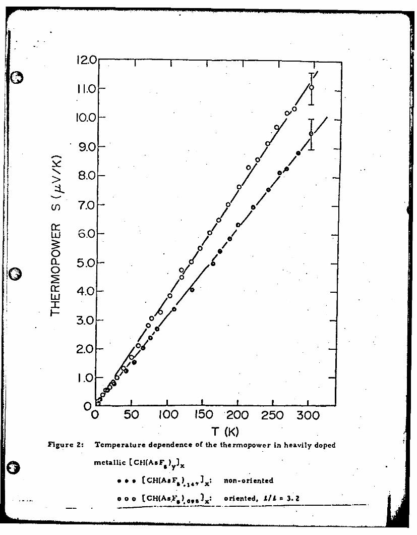
0 The thermopower in the metallic limit is shown in Fig. 2, including
the results for both unoriented cis-CI-I(AsF s }.47 ) x and partially oriented
trans-[ CH(AsF6).o,,)xwith L/1 = 3.2. Any variation between oriented
and unoriented samples is comparable to the variations observed from
sample to sample (indicated by error bars on Fig. 2). No qualitative
difference and no significant anisotropy are observed; S(T) is essentially
the same for oriented and as-grown samples. This is consistent with
expectations. Since thermoelectric power is a zero-current transport
coefficient, interfibril contacts should be unimportant allowing an evaluation
of the intrinsic metallic properties. The magnitude and temperature-
dependence of S (Fig. 2) are characteristic of a degenerate electron gas
0 30,31and are indicative of intrinsic metallic behavior.
For dilute concentrations well below the semiconductor-metal
transition the therrapower is large and essentially temperature independent.
Such behavior can be understood for a dilute concentration of carriers
(holes) which hop among a set of localized states. In this case, where the
kinetic energy of the carriers is negligible, the thermopower is given by
33, 34the Heikes formula
kS = B 1n[(-P/P (1)
where P = n/N is the ratio of the number of holes (n) to the number of
available sites (N) (eq. I assumes spinless carriers; the inclusion of spin
34degeneracy changes the expression to S +(k /Ie)1n(Z-p)/p). Identification
B--
11
with the experimental data for undoped trans-(CH)X requires that p zw 10-4
and temperature independent. This value corresponds to a carrier concen-
tration of 2 x 101-a cm-3 in "undoped" (GH) x and is consistent with the results
35of capacitance vs voltage studies of p-(CH)X: n-CdS heterojunctions using CdS
with known carrier concentration. The results therefore imply that in the
undoped polymer, the conductivity is due to a small number of residual carriers
(Po 10-4) provided by defects and/or impurities, and that the mobility results
from hopping. The insensitivity of the thermopower to iodine concentrations
less than 0. 1 mole% (or 0. 1%1") is consistent with this interpretation and3
implies that po is well below 10 '. From eq. 1, the thermopower at
y = 10 should be 0. 75 of that at y 10 -4 ; consistent with Fig. I to within
the combined uncertainty in y and p.
b) Conductivity
By careful control of thedopant concentration, any specified conduc-
tivity can be obtained covering the range from 0 = 2 x 10⁻⁹ (2- -cm -1 to
a > 10' C "- -cm "7 using cis-(CH) x starting material. Higher metallic values,
>0> 3000 "IL -cm 1t , were obtained using cis starting material, stretch-
oriented (L/Lo = 3. 1) and then doped with AsF s . Since exposure of undoped
(CH) to ammonia vapor2 decreases a to values below 10 "10 O "1 -cm , the
accessible range covers more than thirteen orders of magnitude.
The temperature dependences of AsF. -doped (CH)X, both as-grown,
and stretch-oriented are shown in Fig. 3, for a variety of dopant concen-
trations. The temperature range covered by the measurements depended
on the resistance of the sample; for the highest conductivity sample, data
were obtained over the entire range from 300 to 1. 8 K. The curvature

* .•
1235
seen in log a vs I/T was noted earlier for halogen dopants. This curvature
may arise fromdisorder, for example, leading to a distribution of activation
36energies. Alternatively variable range hopping may play a role at low
temperatures. Taking the initial slope of the log a vs li/T plots, we obtain
the activation energy, AE, which serves as a simple index of the conduc-
tivity behavior. The results are presented in Fig. 4 where data from
AsF.-doped samples and iodine doped samples are plotted versus concen-
tration on a logarithmic scaie. Note that the iodine doped samples are
37formulated as [CH()yl )since the " ion is known to be present. Using
this formulation the data from the two dopants are in good agreement,
although the AsF doped samples give consistently lower activation energies
above y = 0. 01 consistent with the higher metallic conductivity. The
activation energy of the undoped trans-(CH)x is AE (.3 k .03) eV. AE is
relatively insensitive to the dopant concentration up to y = 0. 001, and then
decreases rapidly through the SM transition. Above y = 0.01 (1 mole %)
AE is small and nearly independent of the concentration; the conductivity
is no longer activated in heavily doped (CH) .
The room temperature values from Fig. 3 are replotted as a vs y in
Fig. 5. The value y = 10 - 4 for undoped (CH). was determined from the
34 .
magnitude of the thermopower, as described above; the point at y = 0. 003
was determined by weight uptake. In the dilute concentration regime, a
Oincreases approximately in proportion to the dopant concentration, so that

A13
the mobility is independent of y. Note that in this dilute regime, the
activation energy (Fig. 4) is also insensitive to the dopant.concentration.
Figures 4 and 5, together with the temperature independence of the. thermo-
30power, imply that in the dilute regime the transport is via carrier hopping;
the conductivity results from a temperature independent carrier concentration
38(proportional to y) and an activated mobility.'
The temperature dependence of the conductivity in the metallic
high concentration limit is shown more clearly in Figure 6, where 0/ RT
vs. T is plotted in a linear scale. The room temperature conductivity
value's for these partially oriented films were measured independently by.
39o simple four-probe and by Montgomery techniques. The results, com-
pared in Table 1, are in general agreement. For heavily doped metallic
[CH(AsF-) 0. 4 Ix (oriented with 1/1 = 3. 1), the conductivity first increases
7,31on cooling below room temperature, goes through at maximum at 220 K,
then decreases and becomes constant below 5 K with o(0)/a(300 K) = 0.66.
The conductivity maximum near room temperature varies from sample to
sample, but in general cis-(CH) starting material leads to a larger___ x
maximum than trans-(CH) x . Also shown in Fig. 6 are the results for
[CH(1) s) (tL °I = 3. 1). The conductivity decreases monotonicaliy and3 sx 0
appears to be going to zero as T- 0. The low temperature data from
these samples are shown in more detail in Fig. 7 where we plot the
o normalized conductivity (log scale) vs I/T. For the metallic CH(AsF ) x31
the conductivity at low temperatures approaches the constant value.
*14
a(0) " 800 O -'cm_ 1 . For the iodine doped [CH( )o.O ,Ix' the low temper-
ature conductivity continues to be activated, even though the room temper-
ature value is comparable to that of the AsF 5 doped sample.
Considering the matted fibril structure of polyacetylene the
temperature independence of the conductivity (see Fig. 7) suggests a
tunneling mechanism through the interfibril contact barriers in addition
to the thermally activated charge transfer over the barriers located between
large metallic conducting fibers. The residual activation for heavily doped
ECH(I ) is not understood. However, this may indicate that even the heavily*yx
iodine doped samples are only just on the verge of metallic behavior.
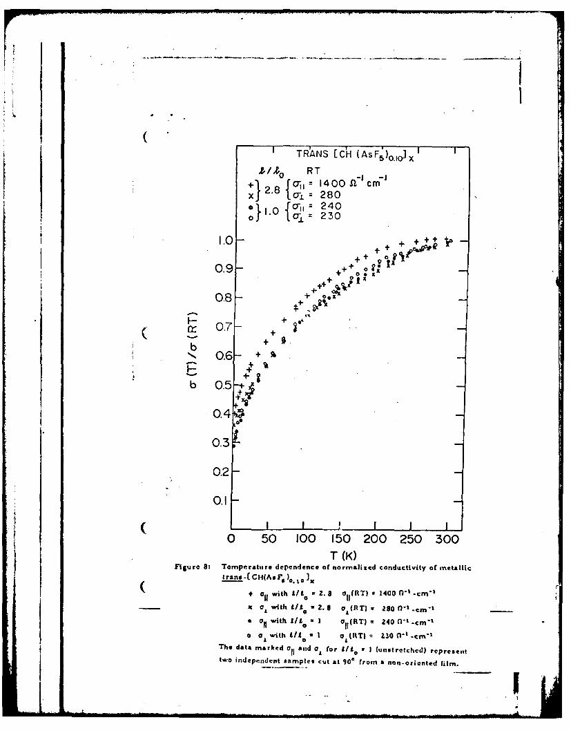
The temperature dependence of the conductivity of trans-CCH(AsF. )
samples, both partially oriented with elongation ratio 1/1o = 2. 8 and
unoriented, are shown in Fig. 8. The two samples were prepared from the
same starting material and were doped simultaneously. The temperature
dependences of the normalized conductivities are similar although the room
temperature values varied considerably (for /L1o = 2. 8, aYI = 1400 n-I -cm- 1
and = 280 -I.cm-I; for 9/1o = 1, a= o 240 fl " -c m - I ). Furthermore,
at low temperatures all four samples approach nearly temperature inde-
pendent behavior as shown in Fig. 9. The low temperature normalized
values are somewhat higher in the oriented samples. These results
indicate that the role of the Interfibril contact barriers are similar in
each direction, and that the barrier height and/or widths are slightly
OF 15
smaller for the partially oriented films. The temperature dependence of
a for a partially oriented film (1/f. ~ 3) which has been exposed to the air
during the isomerization under stress, flattens more slowly resulting in
G(1. 8 K)/(300 K) = 10 . . Combined with the observation of decreasing
tensile strength after air exposure, this result suggests that the cross
linking induced by the air exposure makes the interfibril contact barriers
effectively larger.
Although the temperature dependences of the normalized conduc-
tivities are the same, the room temperature conductivity in the parallel
and transverse direction of the partially aligned films are different about
factor of'five for the 1/t = 2. 8 sample of Figs. 8 and 9. Since the
interfibril contact barriers are same in either direction, the large
difference in absolute magnitude is evidently due primarily to the difference
in total number of chains in the respective directions. Since the films are
not perfectly oriented, there are chains going along the transverse direction
in the partially oriented films. Thus, more complete orientation can be
expected to yield larger values for all and for the anisotropy o/o . In
this context, the thermopower data of Fig. 2 are readily understood. Even
in the tr.ansverse direction a dominates the transport so that S is deter-40
mined by SI. Determination of S will require nearly complete orientation.
The temperature dependences of the normalized conductivity of
trans-[CH(AsF6)y x films are shown in Fig. 10 with values of y spanning
the SM transition. The films were partially oriented to minimize interfibril
*r
ho 16contact effects. A qualitative change in behavior is observed at the SM
transition (y = yc). At low concentrations the curves appear thermally
activated and 0 0 as T-- 0. Above yc, the curvature changes and the
conductivity remains finite as T - 0. The low temperature normalized
conductivity appears to be an excellent indicator of the SM transition in
AsF doped (CH) as shown in Fig. 11. From Fig. II we infer y ' 0. 01-. 02.
Note that, as described above, for the iodine doped samples it appears
that a - 0 as T 0 even at the highest doping levels. Thus, either the
interfibril barrier effects are significantly more important or the metallic
state is not truly achieved even at the highest doping levels.
IV. DISCUSSION
* a) Semiconductor-Metal Transition; Mobility
* The transition from semiconductor to metal is most clearly evident
in the normalized conductivity data of Figs. 10 and 11 obtained from partially
oriented films. The qualitative change in temperature dependence and
finite zero temperature values above yC 0. 01-0. OZ are indicative of an
abrupt change in behavior as a function of dopant concentration. For
41iodine doping the situation is somewhat less clear as noted by others and
described in Section Mb.
We note that the critical concentration, y'c for the SM transition.
as inferred from the conductivity data of Figs. 10 and 11, appears to be
9somewhat below that inferred from the onset of Pauli susceptibility; from
' i.
o17the conductivity data we infer 0. 01 < Yc < 0. 02, whereas the susceptibility
data suggest yc > 0. 02. Additional susceptibility studies are underway to
provide a more detailed and accurate description of the transitional reginme.
Direct measurements of the mobility (e. g. time of flight, etc.)42
are not available. Although Hall effect data have been reported in the
metallic regime, the Hall coefficient is two orders of magnitude below
that expected on the basis of approximately one carrier per dopant and
may be dominated by the fibril structure of the composite medium. Some
important information on the transport mobility in the semiconductor and
metallic limits can be obtained directly from the conductivity.
In lightly doped trans-(CH)x, the mobility is activated as described
in Section IlIb with a room temperature value of 9z = /ne 5 x 10cm/V-secs
(see Fig. 12). For y > 0. 003, one finds a dramatic increase in ti. At
higher dopant levels (i. e. in the transitional regime) AE is changing so
that it is not possible to extract i from the conductivity.
In the metallic regime, e.g. CCH(AsF),.II x the number of carriers
can be estimated by assuming unit charge transfer per dopant or from the
29oscillator strength as obtained from optical studies. The latter results
suggest that in the heavily doped metallic state all the n-electrons contribute
to the metallic transport; thus n(metal) 1- 2 x 1022 cm "L. Taking the intrinsicdc
conductivity to be Ointrinsic ! 2 x 10⁴ 'cm-t as inferred from analysis0
l18292
of the optical data, one obtains P(metal) 6 cm /V-sec. Note that
assuming that all Tr-electrons contribute requires that heavy doping removes
the bond-alternation leading to a uniform bond length polyene. Taking the
somewhat more conservative point of view of one carrier per dopant, the
corresponding value for [CH(AsF s ),. .)x would be n- 2 x 10 *1 with p i
60 cm=2 /V-sec. This latter value is plotted in Fig. 12 as characteristic of
the metallic state.
Although-there is considerable uncertainty in the absolute values
in both limits, the results nevertheless demonstrate a remarkable change
in mobility, five or six orders of magnitude, on going through the trans-
S itional region. This large increase in P represents perhaps the clearest
indication of a major change in electronic structure and/or transport
mechanism at the SM transition in doped polyacetylene.
b) Metallic State
The high mobility in the metallic state is unexpected in view of the
extensive disorder; the doped polymer is only partially crystalline and
contains -- 10116 charged impurities in random interchain positions. Given
7 6,29the considerable evidence of one-dimensionality from transport, optical
43 44and nmr studies, the effects of disorder would be expected to be particularly
large., e
The thermopower data in the high concentration limit provide
0 independent information on the metallic state and are consistent with
V

1930, 31
metallic behavior. For a nearly filled band (i. e. p-type) metallic system,
the thermopower can be written as
S T2 kB dLna(E) (2)S +(-- 1-kTf dE EF
where o(E) = n(E)f e P(E) and n(E) is the number of carriers contributing
to o(E), dn(E)/dE = g(E) is the density of states (both signs of spin) and
PE) is the energy dependent mobility. Assuming energy independent
scattering (M(E) independent of E)
kB --S =+ (T7 ) 7kBT T](F (3)BTT
where ?(EF) = g(EFJ/N is the density of states per carrier. As indicated
30, 31in Fig. 2 and in earlier papers, S is a linear function of T for AsF -dopedS
metallic (CH) whereas for heavy iodine doping there is curvature in S vs T.
Nevertheless, in both cases, the thermopower decreases smoothly toward
zero as T -. 0 in a manner typical of metallic behavior even at temperatures
as low as 2 K. The experimental results (Fig. 2) are in good agreement
with eq. 3 with ri(E F ) = 1. 36 states per eV per carrier. Since there are
0. 15 carriers per carbon atom in [CH(AsF .isJ (assuming complete
charge transfer), the thermopower data yield for the density of states,
g(E F ) 0. 2 states per eV per C atom in good agreement with the value
9obtained from magnetic susceptibility measurements.
20
Although the conductivity is weakly activated below. 50 K and
becomes temperature independent at low temperatures, the thermopower
data imply intrinsic metallic behavior at all temperatures. We therefore
conclude that the dc transport is limited by interfibril contacts, and that
the heavily doped polymer can be described as consisting of metallic strands
29separated by thin potential barriers. This is consistent with optical studies
which indicate that the intrinsic individual strand conductivity is much
higher than the dc value.
A model appropriate to a composite medium consisting of metallic
particles dispersed at high density in an insulating matrix was recently
45developed by Sheng et al. Fluctuation induced tunneling through potential
barriers leads to the bulk dc conductivity at low temperatures with activation
over the barriers at highir temperatures. We identify the conducting aggregates
45of Sheng et al. with the metallic fibrils and assume that the barriers are
45due to interfibril contacts. Sheng et al. assume a parabolic barrier,
V = V -(4Vo/W)xF, where V0 and W are the barrier height and thickness,
respectively. We assume the cross sectional area, A, of the barriers is
typically equal to that of the polymer fibrils whose diameter is -- 200 A.
In terms of these parameters, the conductivity (a.) of the junction can be
expressed as
T
@(T) eT+T (4)
e -J o
21
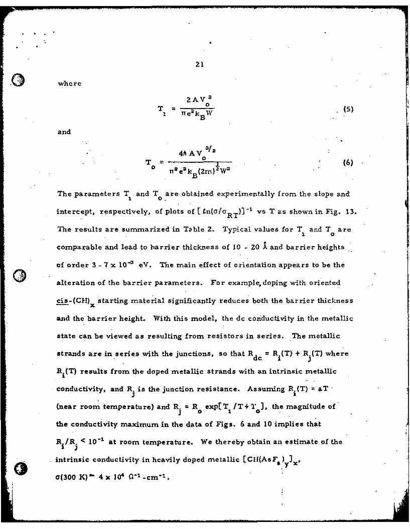
0 where
?AV 2
T 0 (5)i TTea kBW
and
4h AVT 0 )
T2e 2 mk B(2M)W 2
The parameters T and T are obtained experimentally from the slope and1 0.
intercept, respectively, of plots of [ n(ola )]- vs T as shown in Fig. 13.
The results are summarized in Table 2. Typical values for T and T are1 0
comparable and lead to barrier thickness of 10 - 20 A and barrier heights
of order 3 - 7 x 10- eV. The main effect of orientation appears to be the
alteration of the barrier parameters. For example, doping with oriented
cis-(CH)x starting material significantly reduces both the barrier thickness
and the barrier height. With this model, the dc conductivity in the metallic
state can be viewed as resulting from resistors in series. The metallic
strands are in series with the junctions, so that R = Ri(T) + R(T) where
R.(T) results from the doped metallic strands with an intrinsic metallic
conductivity, and R. is the junction resistance. Assuming Ri(T) = aTJ1
(near room temperature) and R. = R exp[T/T+ T o), the magnitude of
the conductivity maximum in the data of Figs. 6 and 10 implies that
R /R. < 10-1 at room temperature. We thereby obtain an estimate of the
intrinsic conductivity in heavily doped metallic CCIl(AsFs)y) x ,
C(300 K)" 4 x 10⁴ 0 ' -cm- 1 .
c) Light Doping, y < 0. 001
In this low concentration regime, the number of carriers is
proportional to the concentration of dopants, and the activation energy
remains constant. Moreover, the temperati t e independent thermopcwer
indicates a temperature independent carrier concentration implying that
the mobility is activated. We therefore conclude that in the dilute
regime
a = nePl (7)
where n is the number of carriers (equal to the number of dopants) and
the mobility is given by
-AE/kT0J =oe (8)
with AE = 0. 3 eV as indicated on Fig. 4. Such a small, thermally activated
mobility is unexpected in a broad bandwidth semiconductor like (CH)X.
Although one might suggest that the activated transport is limited by
disorder in'the polymer, the high conductivity and high mobility in the
metallic state argue to the contrary. One might argue that the observed
activation energy is the result of int .ibril contact resistance. However,
the activation energy is ins* ,tive to whether the polymer is taken as-grown
or stretch-oriented. (Note that the low temperature results in the metallic
regime show major changes in interfibrillar contact effects on orientation;
see Figs. 7, 8, and 9). Moreover, nearly identical results are obtained
0
23
from low density foam-like material synthesized using a gel as an inter-
mediate step; whereas the fibril density is down by more than an order of
46magnitude, and the fibril diameter is three to five times larger.
The localized state hopping transport inferred from the thermopower
9,30,47measurements below y = 0. 001 is qualitatively consistent with the proposed
soliton doping mechanism. Motion of the charged localized domain-walls
would be expected to be via diffusive hopping in agreement with the low
mobility inferred from Fig. 5 for y < 0. 001. Moreover, for a fixed impurity
concentration the number of charged kinks would be independent of
temperature in agreement with the temperature independent the rmopower
found in the dilute limit. Finally, although the domain-wall would be
distributed over a group of carbon atoms, the center of mass of the wall
could take any position along the chain so that the number of available sites
would be of order the number of carbon atoms in agreement with the
magnitude of the thermopower.
The formation of domain-walls, or solitons on long chain polyenes
12 13has been studied theoretically by Rice and by Su, Schrieffer and Hleeger.
The electronic structure of the soliton exhibits a localized state
41o at the center of the gap , containing one electron for the neutral kink.
While this localized state is spin unpaired, the distorted valence band
continues to have spin zero. Thus, the neutral soliton has spin 1/2. The
static susceptibility therefore will contain a Curie law contribution and
can be used to count the number of neutral soliton defects present. Spin L41

24
11 43resonance linewidth and nmr relaxation studies have demonstrated mobile
spin species spread out over many lattice constants in agreement with
these ideas. The number of unpaired spins, typically one per 3000 carbon
atoms is comparable to the number of charge carriers in the undoped
polymer (- one per 10, 000 carbon atoms) inferred from the the rmopower.
Since the localized state occurs at the gap center, i. e. the chemical
potential, the relevance of the solitons to the doping of (CH) x depends on
the energy for creation of a soliton, Es, as compared with the energy13
required for making an electron or a hole, -!Eg = A. Numerical estimates
indicate that soliton formation is energetically favorable, i. e. E < A.
48 sMoreover, Takayama et al. have recently developed a continuum model
2in which they find E = -A; i. e. always less than A.S 1
From these observations we suggest that in the undoped trans-(CH)x,
a fraction of the isomerization induced defects has been ionized by residual
impurities to give the observed density (P - 10 - 4 ). Subsequent doping will
ionize more and/or create additional charged kinks.
In the case of diffusive hopping, the mobility is given by the
Einstein relation, P = eD/kT, where D is the diffusion constant. To obtain
an estimate of the diffusion constant we use the result of Wada and
49Schrieffer (WS) for one-dimensional Brownian motion of domain-walls in
contact with thermal phonons
kBT s
0 D 0.51 6 ,u as ( (9)WS 0 MW 2 U2
0 0
25
where M is the atomic (C-H) mass, u is the equilibrium amplitude of the
distortion and w0 is the attempt frequency. In the double-well Y4 theory
considered by VS, w0 is the harmonic vibration frequency for an atom
near the minimum of either well. In (CH) x, we may take u0 = K/M
is th sprig con 50 4where K 10. 5 eV/., is the spring constant. Wada and Schrieffer 4 9
consider the interaction between neutral, free domain-walls and phonons.
At room temperature using M = 13 AMU, a 1.4 Iland u0 0.041 we
find DWS 2 x 10⁻² cm 2 /sec (Ds/a' - 1014) in agreement with the
measured 4 3 diffusion constant of the neutral magnetic solitons in undoped
trans-(CH)x .
In the case of charged solitons one might argue that the hopping
attempt frequency is reduced by the Coulomb binding of the wall to the
acceptor ion and assume that
• .AE/kBT.D(CH)X Dwse B (10)
so that for lightly doped (CH)x
e -AE/kTM(CH)x BT DWS
2 B -tiE/k T0.516 )W a 2 - 3 e B 011)• kBT o Mw o Uo
r t0
~~For the charged soliton, with iE" 0. 3 eV, D(CH)" 2x10 "' at room
26
temperature leading to a mobility of U 10-5 cm e /V-sec. Although
of the correct magnitude, such a picture would imply hopping between
impurity sites whereas the data indicate that the number of available sites
38is much larger; i. e. comparable to the number of carbon atoms per unit
length on the chain. A detailed understanding of the diffusion (and'mobility)
of charged solitons is clearly lacking. However, we would anticipate that
the activation energy for motion of a charged soliton (on an otherwise13
perfect chain) would be much greater than that of a neutral soliton.
Theoretical study of the charged soliton mobility is required for further
progress.
@The hopping mobility discussed above is appropriate to steady
state (dark) transport in the dilute limit. However, the transport mobility
appropriate to photogenerated carriers may be considerably higher. Since
a soliton-like distortion would be expected to form around a photogenerated
carrier only after a considerable time delay, the band mobility might be
appropriate. Particularly in junctions where the carriers are rapidly
swept out by the junction electric field, a mobility greater than or equal
to that found in the metallic state would be expected.
V. Summary and Conclusion
The transport data presented in this paper indicate three important
concentration regimes:
1) y < 0. 00); the dilute limit where carriers introduced by
doping act independently
2) 0. 001 < y < 0. 01; the transitional region
0 27
3) y> 0.01, the metallic state.
From analysis of the data, we have been able to draw specific conclusions
relevant to these three regimes.
In the dilute limit, the transport is via carrier hopping; the
mobility is small (- 5 x 10⁻⁵ cm 2 IV-s) and activated (AE 0. 3 eV).
This localized state hopping transport is consistent with the proposed
soliton doping mechanism. Based on the soliton interpretation of the
steady state (dark) transport in the dilute limit, it was argued that the
mobility appropriate to photogenerated carriers may be considerably
higher; i. e. greater than or equal to that found in the metallic state.
The semiconductor-metal transition is evident in [ CH(AsF ))
and results in a qualitative change in temperature dependence of the
conductivity and finite zero temperature values above Yc 0. 01 - 0. 02.
For iodine doping the situation is somewhat less clear.
The transport mobility in [ECH(AsF s ) y increases dramatically
on going through the transitional iegion. This large increase (five to six
orders of magnitude) represents perhaps the clearest indication of a major
change in electronic structure and/or transport mechanism at the SM
transition.
The high mobility in the metallic state (- 60 cm s /V-sec assuming
complete charge transfer with one carrier per dopant molecule) provides
-strong evidence of the validity of a band theory approach with delocalized
states in this disordered metallic polymer. Even in this context the
I
28
mobility is surprisingly large; the inferred values are comparable to the.
mobilities found in the best metals (e. g. for copper P - 50 cm2 /V-sec at
room temperature).
The metallic state is described as metallic strands separated by
thin potential barriers (typically W < 20 1 and V < I0-3 eV). Electron0
transfer through the barriers is via tunneling at low temperatures, with
activation over the barriers at higher temperature. The main effect of
orientation appears to be to alter the properties of the barriers. In
particular, doping oriented cis-(CH)x starting material leads to significant
improvement in conductivity due to smaller barrier widths and lower
barrier heights. Analysis of the temperature dependence of the conductivity
within this model leads to an estimate of the intrinsic conductivity in heavily
doped metallic CCH(AsFs)y x , 0 4 x le Q-1 -cm "1 at room temperature.
These and related transport results must be viewed in the context
of the broad based experimental study of the chemical and physical prop-
erties of this new class of conducting polymers. The transport data provide
insight into many aspects of the problem. However, detailed understanding
of the doping mechanism, charge transport, electronic structure, and the
semiconductor to metal transition will require combined input including,
in particular, structural, optical and magnetic information.
o Acknowledgement: We thank S. C. Gau and A. Pron for help in sample
prepa ration.
S
TABLE 1
Comparison of four-probe and Montgomery results fora,, and cyL on oriented samples at room temperature.
'I
4-Probe MontgomeryALl = 3. 1 (0- -cm' L ) (f(I -cm "1 )
cis-[CH(AsF ) t xi[ 2450 23501 - 377
is -CH. Ix O 1500 1620a - 203
1800 2800trans-f CH(AsF ). I10 J. 120 220

TABLE Z
Barrier parameters obtained from analysis of low tcmperaturedata obtained with metallic ( CH(As F) y x
Sample L/1L T 2 T 0 () V0 (eV)
as ( 48.1 41.3 17 7.2 x 10"3 (eV)ras-[H(A~s) !0 ] x 1.0
1 0 47.8 39.0 18 A 7.5 x 10 "
a11 35.0 37.3 16k S. 8x10rans-4C(AsF5 ). io']x 2.8
t02 54.7 54.0 15k 7.2 x l0 "3
cis-CCH(AsF ).) 3.1 a 21.4 48.9 9.2 3. 5 x 10- 3
0~ S.14 x
0 References:
1. Shirakawa, H., Louis, E. J., MacDiarinid, A. G., Chiang, C.. K.,
and Heeger, A. J., Chem. Commun. 578 (1978); Chiang, C. K.,
Druy, M. A., Gau, S. C., Heeger, A. J., Shirakawa, H., Louis,
E. J., MacDiarrnid, A. G. and Park, Y. W., J. Am. Chem. Soc.
100, 1013 (1978)
2. Chiang, C. K., Fincher, C. R., Jr., Park, Y. W., Heeger, A. J.,
Shirakawa, H., Louis, E. J., Gau, S. C. and MacDiarmid, A. G.,
Phys. Rev. Lett. 39, 1098 (1977)
3. Chiang, C. K., Gau, S. C., Fincher, C. R., Jr., Park, Y. W.,
MacDiarmid, A. G. and Heeger, A. 3., App. Phys. Lett. 33, 181
(1978)
4. Ozaki, M., Peebles, D., Weinberger, B. R., Chiang, C. K., Gau,
S. C., Heeger, A. 3. and MacDiarrid, A. G., Appl. Phys. Lett.
35, 83 (1979)
5. Shirakawa, H., Ito, T., Ikeda, S., Polym. 3. 4, 460 (1973)
6. Fincher, C. R., Jr., Peebles, D. L., Heeger, A. J., Druy, M. A.,
Matsumura, Y., MacDiarmid, A. G., Shirakawa, H. and Ikeda, S.,
Solid State Commun. 27, 489 (1978)
7. 'ark, Y. W., Druy, M. A., Chiang, C. K., Heeger, A. 3.,
MacDiarmid, A. G., Shirakawa, H. and Ikeda, S., Polymer Lett.
S17, 195 (1979)
8. Grant, P. M. and Batra, I. P., Solid State Commun. 29, 225 (1978)
9. Weinberger, B. R., Kaufer, J., Heeger, A. J., Pron, A. and
MacDiarmid, A. G., Phys. Rev. B 20, 223 (1979)
10. Goldberg, I. B., Crowe, H. R., Newman, P. R., Heeger, A. 3.
and MacDiarmid, A. G., J. Chem. Phys. 70, 1132 (1979)
11. Weinberger, B. R., Kaufer, J., Heeger, A. 3. and MacDiarmid,
A. G., Phys. Rev. Lett. (Submitted)
12. Rice, M. J., Phys. Lett. 71A, 152 (1979)
13. Su, W. P., Schrieffer, J. R. and Heeger, A. J., Phys. Rev. Lett.
42, 1698 (1979)
O 14. Tani, T., Cill, Wt. D., Clarke, T. C., and Street, G. B., Preprint,
IBM Symposium on Conducting Polymers, March 29, 30, 1979
15. Chien, S. N., Heeger, A. J., Kiss, Z., MacDiarrnid, A. G., Gau,
S. C. and Peebles, D. L., Appl. Phys. Lett. (to be published)
16. Shirak'awa, H. andIkeda, S., Polym. 3. 2,'231 (1971)
17. T. Ito, H. Shirakawa and S. Ikeda, Kobunshi Ronbunsha 5, #6 (1976)
p. 470 (English edition)
18. Ito, T., Shirakawa, H. and Ikeda, S., J. Polym. Sci. Polym. Chem.
Ed. 12, 11 (1974)
19. Ito, T., Shirakawa, H. and Ikeda, S., J. Polym. Sci. Polym. Chem.
Ed. 13, 1943 (1975)
20. Shirakawa, 1. , Ito, T. and Ikeda, S., Die Macromoleculare Chemie
179, 1565 (1978)
21. Druy, M. A., Tsang, Chi-Hwa, Brown, N., Heeger, A. J. and
MacDiarmid, A. G., J. Polym. Sci. Polym. Phys. Ed. (in print)
22. Karasz, F. E., Chien, J. C. W., Galkiewicz, R., Wnek, G. E.,
Nature (in press)
23. Shirakawa, H. and Ikeda, S., ACS-CSJ Chemical Congress, Honolulu,
Hawaii, April 1-6 (1979)
24. MacDiarmid, A. G., and Heeger, A. J., Preprint, IBM Symposium
on Conducting Polymers, March 29, 30 (1979)
25. Hsu, S., Signorelli,' A., Pez, G. and Baughman, R., J. Chem. Phys.
68, 5405 (1978); Baughnan, R. H. and Hsu, S. L., Polym. Lett. 17,
.185 (1979)
%4r26. Mihaly, L., Pekker, S. and Janossy, A., J. of Synthetic Metals
(in press)
27. Salaneck, W. R., Thomas, H. R., Bigelow, R. W., Duke, C. B.,
Plummer, E. W., Heeger, A. J. and MacDiarmid, A. G., J. Chem.
Phys. (in press)
28. Salaneck, W. R., Thomas, H. R., Duke, C. B., Paton, A., Plummer,
E. W., Heeger, A. J. and MacDiarrrdd, A. G., J. Chem. Phys. 71,
2044 (1979)
29. Fincher, C. R., Jr., Ozaki, M., Tanaka, M., Peebles, D. L.0
Lauchlan, L., kleeger, A. J. and MacDiarmid, A. G., Phys. Rev. B
20, 1589 (1979)0
30. Park, Y. W., Denenstein, A., Chiang, C. K., Heeger, A. J. and
MacDiarmid, A. G., Solid State Commun. 29, 747 (1979)
31. Kwak, J. F., Clarke, T. C., Greene, R. L. and Street, G. B.,
Solid State Commun. 31, 355 (1979)
7Z. Chiang, C. K., Park, Y. W., Heeger, A. J., Shirakawa, H., Louis,
E. J. and MacDiarmid, A. G., J. Chem. Phys. 69, 5098 (1978)
33. Heikes, R. , Buhl International Conference on Materials, edited by
E. R. Shatz (Gordon and Breach, New York, 1974)
34. Chaikin, P. M. and Beni, G., Phys. Rev. B 13, " 27 (1976)
35. Ozaki, M., Peebles, D. L., Weinberger, B. R., Heeger, A. J.
and MacDiarmid, A. G. (to be published)
36.- Mott, N. F., Philos. Mag. 19, 835 (1969); Mott, N. F., in
Festkrperprobleme, edited by J. H. Queissen (Pergamon, New
York, 1969), Vol. 9., p. 22; Ambegaokar, V., Halperin, B. I. and
Langer, J. S., Phys. Rev. B4, 2612 (1971)
37. Hsu, S. L., Signorelli, A. J., Pez, G. P. and Baughman, R. H.,
J. Chem. Phys. 69, 106 (1978);*Shirakawa, H., Sasaki, T. and
Ikeda, S., Chem. Lett. (Japan) p. 1113 (1978); Harada, I., Tasurni,
M., Shirakawa, H. and Ikeda, S., Chem. Lett. (Japan) 1411 (1978)
38. As discussed above, the value Po 10- 4 (2 x 101 carriers per cm)
for "undoped" trans-(CH)x was determined from the magnitude of the
thermnopower and independently verified from C vs V measurements
on p-n heterojunctions. In our earlier paper (ref. 30) we estimated
10- < p < 10 "3 based on uncertainties at that time on the boundaries
of the dilute regime. However, the insensitivity of the activation
energy (AE) to y (see Fig. 4) below y = 0. 001 clearly identifies this
as the dilute regime. For y > 0. 001, AE begins to fall dramatically
indicative of the importance of dopant-dopant interactions. This
independently demonstrates that P0 is well below 10-3 and implies
that the number N of available sites is comparable to the number of
carbon atoms per unit length in the polymer chain.
39. Montgomery, H. C., J. Appi. Phys. 42, 2971 (1971)
40. Thernoelectricity: An Introduction to the Principles, edited by
D. K. C. MacDonald, (John Wiley and Sons, Inc., New York and
London) p. 115
41. Mihaly, G., Vancso, G., Pekker, S. and J~nossy, A., J. of
Synthetic Metals (in press)
42. Seeger, K., Gill, W. D., Clarke, T. C., Street, G. B., Solid
State Commun. 28, 873 (1978)
43. Nechtschein, M., Devreux, F., Greene, R. L., Clarke, T. C. and
Street, G. B., Phys. Rev. Lett. (Submitted)
44. Mott, N. F. and Twose, W. D., Adv. Phys. 10, 107 (1961);
Borland, R. in Mathematical Physics in One Dimension, ed. by
E. N. Lieb and D. C. Mattis (Acad. Press, N. Y., 1966) p. 319
o 45. Sheng, P., Sichel, E. K.. and Gittleman, J. 1., Phys. Rev. Lett. 40,
1197 (1978); Sichel, E. K., Gittleman, J. I. and Sheng, P., Phys.
Rev. B 18, 5712 (1978); Sheng, P., Phys. Rev. B (Submitted)

46. Wnek, G. E., Chien, J. C. W., Karasz, F. E., Druy, M. A.,
Park, Y. W., MacDiarmid, A. G. and Hecger, A. 3., J. Polymer
Sci.; Polymer Letts. Ed. 17, 779 (1979)
47.. Pincher, C. R., Jr., Ozaki, M., Ifeeger, A. J. and MacDiarrnid.
A. G., Phys. Rev. B 19. 4140 (1979)
48i Takayama, H., Lin-Liu, Y. R. and Maki, K., Phys. Rev. B
(Submitted)
49. Wada, Y. and Schrieffer, J. R., Phys. Rev. B 18, 3897 (1978)
50. Ooshika, Y., J. Phys. Soc. JapanR1, pp. 1238, 1246 (1957)

OFigure Captions:
Figure 1: Thermopower (S) vs y for [CH( 3 ) y )x at room temperature.
Figure 2: Temperature dependence of the thermopower in heavily doped
metallic [CH(AsF ) yx
0 0 & [CH(AsFr) I)x: non-oriented
o o o [CHI(AsF 5 ) 0 3 ] x ; oriented, LI/ 3.2
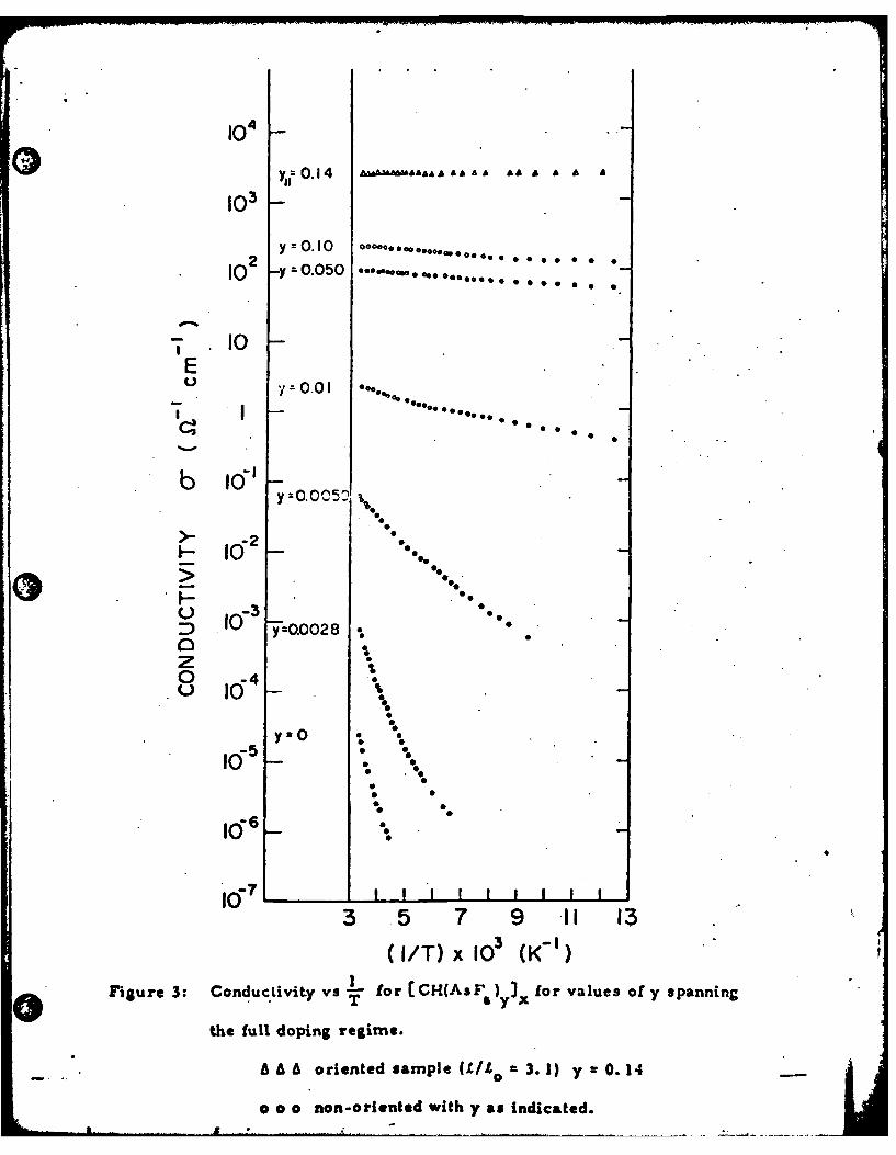
Figure 3: Conductivity vs -I- for[ CH(AsF )yI for values of y spanningT y x
the full doping regime.
A A A oriented =arnole ( -to = 3. 1) y - 0.14
o o o non-oriented with y as indicated.
O Figure 4: Activation energy vs y for [CH(ASFy )x and [CH( )yIx.
o o o trans-[CH(AsFi)yIx; data obtained from Fig. 3.
. . trans-[CH(I 3 Y.; data obtained from ref. 35.
Figure 5: Room temperature conductivity vs y, in the dilute limit, for
[ CH(AsF) yx . The solid line has slope of unity indicating
that initially a is approximately proportional to y.
Figure 6: Temperature dependence of the normalized conductivity of
heavily doped metallic (CH) x
e (CH(AsF) 0 .1 4x; a RT = 2450 W" -cm 1
ooo CH(I)oslx ; aRT = 1500 0 -cm- 1
Both samples were made from oriented cis starting material
Q with t,/, 0 - 3. 1.
Figure 7: Low temperature conductivity of the metallic samples of
Figure 6.
Figure 8: Temperature dependence of normalized conductivity of metallic
trans-[ CH(AsF S )o. o Ix
+ aC; with / =2. 8 aI(RT) 1400 0-1 -cm "-
x with I A 02.8 a (RT) = 280 C-1-cm "-
* Oi, with f/1= 1 CY (RT) = 240 0-1 -cm -
o ar with A/I = 1 o (RT) = 230 Q-1 cm-1
-2" data marked a and for 1!10 I (unstrXt:',cd) represent
two independent samples cut at 900 from a non-oriented film.
Figure 9: Low temperature conductivity of the metallic sample of
Figure 8.
Figure 10: Normalized temperature dependence of trans- CH(AsF ) 1sYx
for I/to = 3. 0.
A A A y=0
xxx y .0 04
a 0 y= 0.008
000 y0.03
+++ y= 0.10
Figure 11: Low temperature conductivity (normalized) vs concentration.
The onset of finite conductivity vs T 0 is indicative of the
semiconductor-metal transition
Figure 12: Transport mobility vs concentration (see text).
0 0 * trans -r CF(AsFs) YI
000 trans-[CH(l ) Iyx
Figure 13: -(mIcl/a RT - vs T; .this plot allows evaluation of the
junction barrier parameters (see text).

46b
04
Q dJ
00
0*N L~-I
.0
(A/A'd)~( S iM~i.3
CIS [CH (AsF) 0 )
CIS (CHIo 2 J
.1 /190 3.
00
0021
0 010203Q 50
N. ( -'
Fiure7 L wte p rtu ecod ctvtyo he m talc a plso
0iue6

*Q -
* 1.1 IIso 0s 6 00 00
01.0 0 0 0
0.9 6?
* 1, •• °
, 00 O
.0 0
0 .0
070
0
0.6-
b•\ 0.5
0.4-0
03 03
" • CIS [CH(AsF )0,4]xR 2450 cmQ2-0
CIS [CHIo.2 5 ]x O'RT = .15 0 0 Sf cm-!
0 .1 . I-t 120, = 3 .1-
0 50 100 150 200 250 300
T (K)Figure 6: Temperature dependence of the normalized conductivity of
heavily doped metallic (CH)x
o0 E (CH(AsFG). 141x; aRT 2450 O -cm "1
0 0o [ CH( kIo 6 ; 'RT = 1500 O'L crn-1
Both samples were made from'oriented cis starting material
with •3.1.
0. S

10
10.Io
10 1
c: .Io-3 1b
* o-4
I-4 1-3 1o-2 107
CONCENTRATION (y)
"Figure 5: Room temperature conductivity vs y, in the dilute limit, for
ECH(AsF) y x . The solid line has slope of unity indicating
that Initially a Is approximately proportional to y.
V)Y) 000
00
9Id
* 0 C
zz0 tor~4
00 000
00
LO~~ 0 o
o
(AO 3V A033NUA
104
f ~ ~ ~ l 0,=.,14 &.-,,,, ,, ,103
y =0.I0 .oMoMo,,,, ,o oo ,,2i yO.I "oa...*~ .. . . . .
10 -y 0.050 " ,, ,o .. , * * * * •
7E 0
EI) y,' 0.01 o, 0,
b 16' y :0.005 %
00
L_ i0 2 ... *
C.) -300 1"4
y 0 ".* 0
y=O*. .'
00
* .%
3 .5 7 9 11 13
I/T) x le 3 (K- ' )
Figure 3: Conduc.Livity vs L for [CH(AsF ) I for values of y spanning
T sy x
the full doping regime.
6 A A oriented sample (L/i 0 3. 1) y : 0. 14
o o o non-oriented with y as indicated.
12.0
11.0 /I1.0 - 01
0
9.0-> /x> 8.0- ,.
Lo 7.0- o/ o/
uJ .0-LL) 0
0 0 .1 0 ./
/000.0-
0 50 100 150 200 250 300T (K)
Figure 2: Temperature dependence of the the rmopowver in heavily doped
mectallic [CCJ(AsF ) J I0 * 0 -CH(ASF* . non-oriented
00 o o CH(As.sgIx, : oriented, Allt 3. 2
IT RANS [C (AsFs)olo]x
2,/4,0 RT+ 2"8 = 1400 ,- cm
1.0 . = 240
4 {aT 230
1.0- + ++t t -
0.9- ++ o g.9+ 0 x
-- + +
b +
0.6- +
+
0.- +
0.5 -.
0.2
01-
0 50 100 150 200 250 300T (K)Figure 8: Temprature dependence of normalized conductivity o metallic
t rans -[ C l(A , , )o. 10 • xanoi with I/ Io 2 . 8 01l(11T) s 1400 n-" -cm"-1'
* 0 1 w th I/ s° 2 . 8l a ( R T ) = 2 8 0 0 1- e~ m - l
* a ll with / 1° 0 1 a 1I(RT) 40 (- -m -%
4 a t with LIA O 1 0 O M Z 0 /S"1 -cm -1
Th * dart m arked a1 a d a I for / te 2 1 (unstretched) represent
two indepe dent amPle0 cut at 90 fro n a non-orented ilm./

0.0+X cp
< ~+c
+K4- .. o C).8+
0 0
04. o c
La. 00 +0.o~ bo- K4
+ 0
~EO +
U) ~ 0 C)0.
-0 0
"

0/
xO.004 TRANS [CH(AsF 5 )y x .0.008 2Ito= 3.0
0 0.031.0 + 0.10 + + + + 0
++ 00++ 0 0 0
0.9 0
+ +0 . 0 o ° x
+ 00.8++ .0
0+o
F--+ 0
0.6 + 00 x
+ 00- 0.5 0+ 0
b0 f 00.4- 0
0.3 0
0 ,
0.2 -0 x0 0
0.1 e 0 x
to 1 x x x I X
0 50 100 150 200 250 300T (K)
Figure 10: Normalized temperature dependence of trans-CCH(AsF.) 1)xfor it/1 3.0.
h66 y:0X x x y O. 004
ooo y= 0.008
000 y=O. O3
+.++ y wo. 0

0~ 9 a
X
0
U) 0
< Z
o 0
xr 0 0
LOC K)dt 00
18) ~~~ -0( Ut)
00 4

0 TRANS [CH (AsF.)y.]x
OTRANS (CH(I 3 )y]x102
0 0
I0 7777/S-M
TRANS-ITION
101Eu~U
1030
I-4
-J 0"
01
I--4
01
10"5 14 i 1 1.10 - 4 10-3 10,.2 Id" I
CONCENTRATION (y)' Figure 12: Transport mobility vs concentration (see text).
& 0 trns-r.CH(AsF)) 3
ooo trn c-H(C,) I .i

o cis [ CH (AsF 5 ) 0.141 x 'I/2Co 3.1
o trans [ CH (As F) 0.o0 x I/40= 2.8
* trans [CH(As F5 )0 10 ] x .4/2 0 = 2.1
5.0-
4.0
\ 3 .0- /
C0
2.0-
00a-|
I I I I II
0 10 20 30 40 50 60 70
T (K)Figure 13: -[Ana JRT] "- vs T; this plot allows evaluation of the
junction barrier parameters (see text).
7-'2/A23 472:GAN: 76: t;
78u472-608
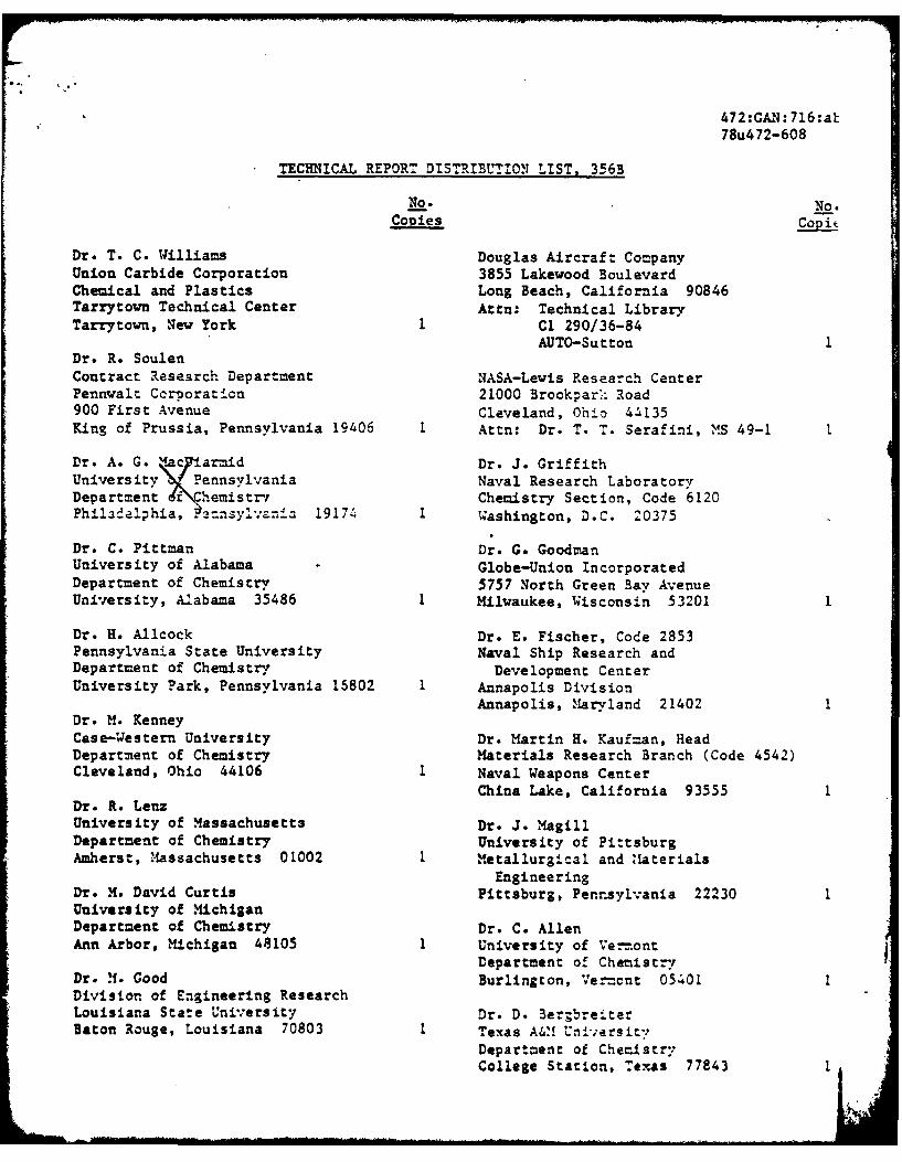
TECHNICAL REPCRT DISTBUTION LIST. GEN
No. No-CoDies CoDie
Office of Naval Research U.S. Army Research OfficeAttn: Code 472 Attn: CRD-AA-lP800 North Quincy Street P.O. Box 1211Arlington, Virginia 22217 2 Research Triangle Park, N.C. 27709
ONR 3ranch Office Naval Ocean Systems CenterAttn: Dr. George Sandoz Attn: Mr. Joe McCartney536 S. Clark Street San Diego, California 92132Chicago, Illinois 60605
Naval Weapons CenterC:,7. 3-ranch O Z.4ice Attn: Dr. A. 3. -A--scer,
At -a: Sciam-ic Dept. Chemistry Division7153 3roadway China Lake, California 93555.!'ew York, .New Tork 10003
Naval Civil Engineering LaboratcryOR: Branch Office Attn: Dr. R. W. Dr .sko:030 East Gr.en Street Port Fuene, California 93401Pasadena, California 91106
Department of Physics & ChemistryONR Branch Office Naval Postgraduate SchoolAttn: Dr. L. H. ?aebles Monterey, California 93940Building 114, Section D666 Su-mner Street Dr. A. L. SlafkoskvBoston, Massachusetts 02210 1 Scientific Advisor
Commandant o! the Marine CorpsDirectcr, Naval Research Laboratory (Code RD-1)Attn: Code 6100 Washington, D.C. 20380Washington, D.C. 20390 1
Office of Naval ResearchThe Assistant Secretar-I Attn: Dr. Richard S. Miller
of the Na'vy (R,-&S) 800 N. Quincy StreetDepartment of the Navy Arlington, Virginia 22217Room 4E736, ?entagonWashington, D.C. 20350 1 Naval Ship Research and Development
CenterCommandar, :a-'l Air Systems Ccmmand Attn: Dr. G. Bosmazian, AppliedAttu: Code 3'.C (M_. Rosenwasser) Chemistry DivisionDepartment of the NaMv7 Annapolis, Maryland 214.01Washington, D.C. 20360 1
Naval Ocean Systems CenterDefense Documentation Center At%.n: Dr. S. Yama-oto, MarineBuilding 5, Cameron Staccn Sciences D:i'-*ionAleandrla, V1r;ia .3I4 12 San Diego, Callifoi'a 91232
r. 7red Saal.el! Mr. John BcvieChemisy :i--aon :M.a:erials 3ranch:aval Resuart.h .a-rac:r'. Naval Shin --;naerln; Can:-er*;ashi3$mon, D.Z. 0375 ?hadei...a, cnns:1vanla 1911
472:GAN: 716:a
78u472-608
TECHNICAL REPORT DISTRIBUTION LIST. 3563
No. No.
Copies Cop i
Dr. T. C. Williams Douglas Aircraft CompanyUnion Carbide Corporation 3855 Lakewood BoulevardChemical and Plastics Long Beach, California 90846Tarrytown Technical Center Attn: Technical LibraryTarrytown, New York Cl 290/36-84
AUTO-SuttonDr. R. SoulenContract Research Department NASA-Lewis Research CenterPennwalt Corporation 21000 Brookpar. Road900 First Avenue Cleveland, Ohio 4.,135King of Prussia, Pennsylvania 19406 1 Attn: Dr. T. T. Serafini, IMS 49-1
Dr. A. G. Mac"i'armid Dr. J. GriffithUniversity fPe onsylvania Naval Research LaboratoryDepartment ifiChemistrv Chemistry Section, Code 6120Philadelphia, 3=nsy'vania 19174 1 Washington, D.C. 20375
Dr. C. Pittman Dr. G. GoodmanUniversity of Alabama Globe-Union IncorporatedDepartment of Chemistry 5757 North Green Bay AvenueUniversity, Alabama 35486 1 Milwaukee, Wisconsin 53201
Dr. H. Allcock Dr. E. Fischer, Code 2853Pennsylvania State University Naval Ship Research andDepartment of Chemistry Development CenterUniversity Park, Pennsylvania 15802 1 Annapolis Division
Annapolis, Maryland 21402Dr. H. KenneyCase-Western University Dr. Martin H. Kauf-an, HeadDepartment of Chemistry Materials Research Branch (Code 4542)Cleveland, Ohio 44106 1 Naval Weapons Center
China Lake, California 93555Dr. R. LenzUniversity of Massachusetts Dr. J. MagillDepartment of Chemistry University of Pi:tsburgAmherst, Massachusetts 01002 1 Metallurgical and 'Materials
EngineeringDr. N. David Curtis Pittsburg, Pennsylvania 22230University of MichiganDepartment of Chemistry Dr. C. AllenAnn Arbor, Michigan 48105 1 University of Vermont
Department of ChemistryDr. M1. Good Burlington, Ve.-cnt 05401Division of Engineering ResearchLouisiana State University Dr. D. Ber;breiterBaton Rouge, Louisiana 70803 1 Texas A&M Universit-.
Department of ChemistryCollege Station, 7exas 77843 1
472 :GAN:716:ah
78u472-608
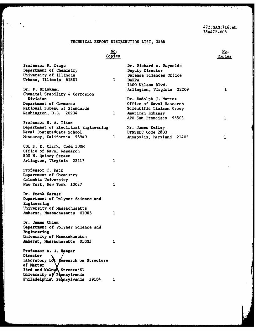
TECHNICAL REPORT DISTRIBUTION LIST, 356B
No. No.Copies Copies
Professor R. Drago Dr. Richard A. ReynoldsDepartment of Chemistry Deputy DirectorUniversity of Illinois Defense Sciences OfficeUrbana, Illinois 61801 1 DARPA
1400 Wilson Blvd.Dr. F. Brinkman Arlington, Virginia 22209 1Chemical Stability & CorrosionDivision Dr. Rudolph J. Marcus
Department of Commerce Office of Naval ResearchNational Bureau of Standards Scientific Liaison GroupWashington, D.C. 20234 1 American Embassy
APO San Francisco 96503Professor H. A. TitusDepartment of Electrical Engineering Mr. James KelleyNaval Postgraduate School DTNSRDC Code 2803Monterey, California 93940 1 Annapolis, Maryland 21402
COL B. E. Clark, Code 100MOffice of Naval Research800 N. Quincy StreetArlington, Virginia 22217
Professor T. KatzDepartment of ChemistryColumbia UniversityNew York, New York 10027 1
Dr. Frank KaraszDepartment of Polymer Science andEngineeringUniversity of MassachusettsAmherst, Massachusetts 01003 1
Dr. James ChienDepartment of Polymer Science andEngineeringUniversity of MassachusettsAmherst, Massachusetts 01003 1
Professor A. J. H egerDirectorLaboratory fo %search on Structureof Matter33rd and Walny Streets/KlUniversity XoP nsylvaniaPhiladelph , Pe sylvania 19104 1