I-7000 and M-7000 DIO User Manual - ICP DAS
198
I-7000 and M-7000 DIO User Manual, Rev: B2.7 7PH-013-B27 1 I-7000 and M-7000 DIO User Manual Warranty All products manufactured by ICP DAS are under warranty regarding defective materials for a period of one year from the date of delivery to the original purchaser. Warning ICP DAS assumes no liability for damages resulting from the use of this product. ICP DAS reserves the right to change this manual at any time without notification. The information furnished by ICP DAS is believed to be accurate and reliable. However, no responsibility is assumed by ICP DAS for its use, or for any infringements of patents or other rights of third parties resulting from its use. Copyright Copyright 1999 - 2011 ICP DAS. All rights reserved. Trademark The names used for identification only may be registered trademarks of their respective companies. Date: 2017/8/7
-
Upload
trinhkhanh -
Category
Documents
-
view
237 -
download
2
Transcript of I-7000 and M-7000 DIO User Manual - ICP DAS
I-7000 and M-7000 DIO User Manual, Rev: B2.7 7PH-013-B27 1
I-7000 and M-7000 DIO User Manual
Warranty
All products manufactured by ICP DAS are under
warranty regarding defective materials for a period of one
year from the date of delivery to the original purchaser.
Warning ICP DAS assumes no liability for damages resulting
from the use of this product. ICP DAS reserves the right to
change this manual at any time without notification. The
information furnished by ICP DAS is believed to be accurate
and reliable. However, no responsibility is assumed by ICP
DAS for its use, or for any infringements of patents or other
rights of third parties resulting from its use.
Copyright Copyright 1999 - 2011 ICP DAS. All rights reserved.
Trademark The names used for identification only may be registered
trademarks of their respective companies.
Date: 2017/8/7
I-7000 and M-7000 DIO User Manual, Rev: B2.7 7PH-013-B27 2
Table of Contents 1. Introduction ...................................................................................... 7
1.1 More Information ..................................................................... 8
1.2 Terminal Assignment ............................................................... 9
1.3 Specifications ......................................................................... 32
1.4 Block Diagrams ...................................................................... 42
1.4.1 Block Diagram for the I-7041/41D, I-7041P/41PD, M-
7041/41D and M-7041P/41PD ............................................... 42
1.4.2 Block Diagram for the I-7042/42D ............................... 42
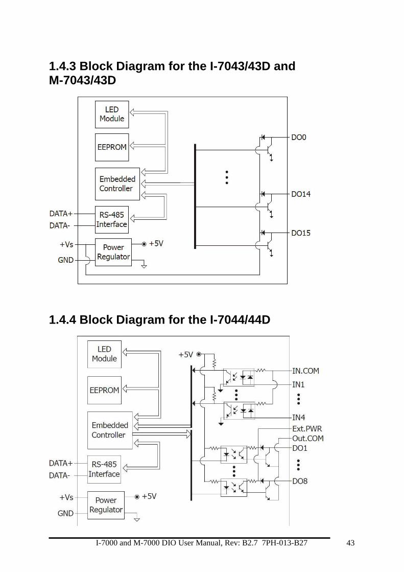
1.4.3 Block Diagram for the I-7043/43D and M-7043/43D . 43
1.4.4 Block Diagram for the I-7044/44D ............................... 43
1.4.5 Block Diagram for the I-7045/45D and M-7045/45D . 44
1.4.6 Block Diagram for the M-7046 and M-7046D ............. 44
1.4.7 Block Diagram for the I-7045-NPN/45D-NPN and M-
7045-NPN/45D-NPN ............................................................. 45
1.4.8 Block Diagram for the I-7050/50D and M-7050/50D . 45
1.4.9 Block Diagram for the I-7050A/50AD ......................... 46
1.4.10 Block Diagram for the I-7051/51D and M-7051/51D46
1.4.11 Block Diagram for the I-7052/52D and M-7052/52D 47
1.4.12 Block Diagram for the I-7053_FG/53D_FG and M-
7053/53D ................................................................................ 47
1.4.13 Block Diagram for the M-7054/54D and M-
7054P/54PD ............................................................................ 48
1.4.14 Block Diagram for the I-7055/55D and M-7055/55D48
1.4.15 Block Diagram for the I-7055-NPN/55D-NPN and M-
7055-NPN/55D-NPN ............................................................. 49
1.4.16 Block Diagram for the M-7055U/55UD ..................... 49
1.4.17 Block Diagram for the I-7058/58D and M-7058/58D50
1.4.18 Block Diagram for the I-7059/59D and M-7059/59D50
1.4.19 Block Diagram for the I-7060/60D, M-7060/60D, and
M-7060P ................................................................................. 51
1.4.20 Block Diagram for the I-7061/61D and M-7061/61D51
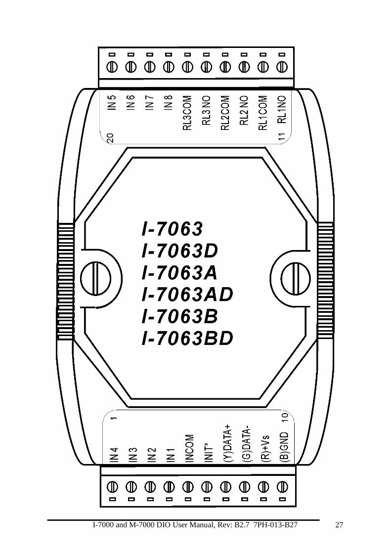
1.4.21 Block Diagram for the I-7063/63D ............................. 52
1.4.22 Block Diagram for the I-7063A/63AD ....................... 52
1.4.23 Block Diagram for the I-7063B/63BD ....................... 53
1.4.24 Block Diagram for the M-7064/64D........................... 54

I-7000 and M-7000 DIO User Manual, Rev: B2.7 7PH-013-B27 3
1.4.25 Block Diagram for the I-7065/65D ............................. 54
1.4.26 Block Diagram for the I-7065A/65AD ....................... 55
1.4.27 Block Diagram for the I-7065B/65BD ....................... 55
1.4.28 Block Diagram for the I-7066/66D and M-
7066P/66PD ............................................................................ 56
1.4.29 Block Diagram for the I-7067/67D and M-7067/67D56
1.4.30 Block Diagram for the M-7068/68D and M-7069/69D
................................................................................................ 57
1.5 Dimensions ............................................................................. 58
1.5.1 Modules without Frame Ground ................................... 58
1.5.2 Modules with Frame Ground ........................................ 59
1.6 Wiring ..................................................................................... 60
1.6.1 I-7041/41D, I-7041P/41PD, M-7041/41D and M-
7041P/41PD wiring ................................................................ 60
1.6.2 I-7042/42D wiring ......................................................... 60
1.6.3 I-7043/43D and M-7043/43D wiring ............................ 60
1.6.4 I-7044/44D wiring ......................................................... 61
1.6.5 I-7045/45D and M-7045/45D wiring ............................ 61
1.6.6 I-7045-NPN, I-7045D-NPN, M-7045-NPN and M-
7045D-NPN wiring ................................................................ 62
1.6.7 M-7046/46D wiring ...................................................... 62
1.6.8 I-7050/50D and M-7050/50D wiring ............................ 63
1.6.9 I-7050A/50AD wiring ................................................... 63
1.6.10 I-7051/51D and M-7051/51D wiring .......................... 63
1.6.11 I-7052/52D and M-7052/52D wiring .......................... 64
1.6.12 I-7053_FG/53D_FG and M-7053/53D wiring ........... 64
1.6.13 M-7054/54D and M-7054P/54PD wiring ................... 65
1.6.14 I-7055/55D and M-7055/55D wiring .......................... 65
1.6.15 I-7055-NPN, I-7055D-NPN, M-7055-NPN and M-
7055D-NPN wiring ................................................................ 66
1.6.16 M-7055U/55UD .......................................................... 67
1.6.17 I-7058/58D, I-7059/59D, M-7058/58D and M-
7059/59D wiring .................................................................... 68
1.6.18 I-7060/60D and M-7060/60D wiring .......................... 68
1.6.19 M-7060P wiring .......................................................... 69
1.6.20 I-7061/61D and M-7061/61D wiring .......................... 69
1.6.21 I-7063/63D, I-7063A/63AD, I-7063B/63BD, I-
7065/65D, I-7065A/65AD and I-7065B/65BD wiring ......... 70
I-7000 and M-7000 DIO User Manual, Rev: B2.7 7PH-013-B27 4
1.6.22 M-7064/64D wiring .................................................... 70
1.6.23 I-7066/66D, I-7067/67D, M-7066P/66PD and M-
7067/67D wiring .................................................................... 71
1.6.24 M-7068/68D and M-7069/69D wiring ....................... 71
1.6.25 Wiring Recommendations ........................................... 71
1.7 Jumper Setting ........................................................................ 72
1.8 Quick Start .............................................................................. 73
1.9 Default Settings ...................................................................... 75
1.10 Configuration Tables ............................................................ 76
1.11 DIO Active States ................................................................. 79
1.12 M-7000 Notes ....................................................................... 80
1.12.1 Protocol Switching ...................................................... 80
1.12.2 INIT Mode ................................................................... 81
1.13 Mounting .............................................................................. 82
1.13.1 Din-Rail Mounting ...................................................... 82
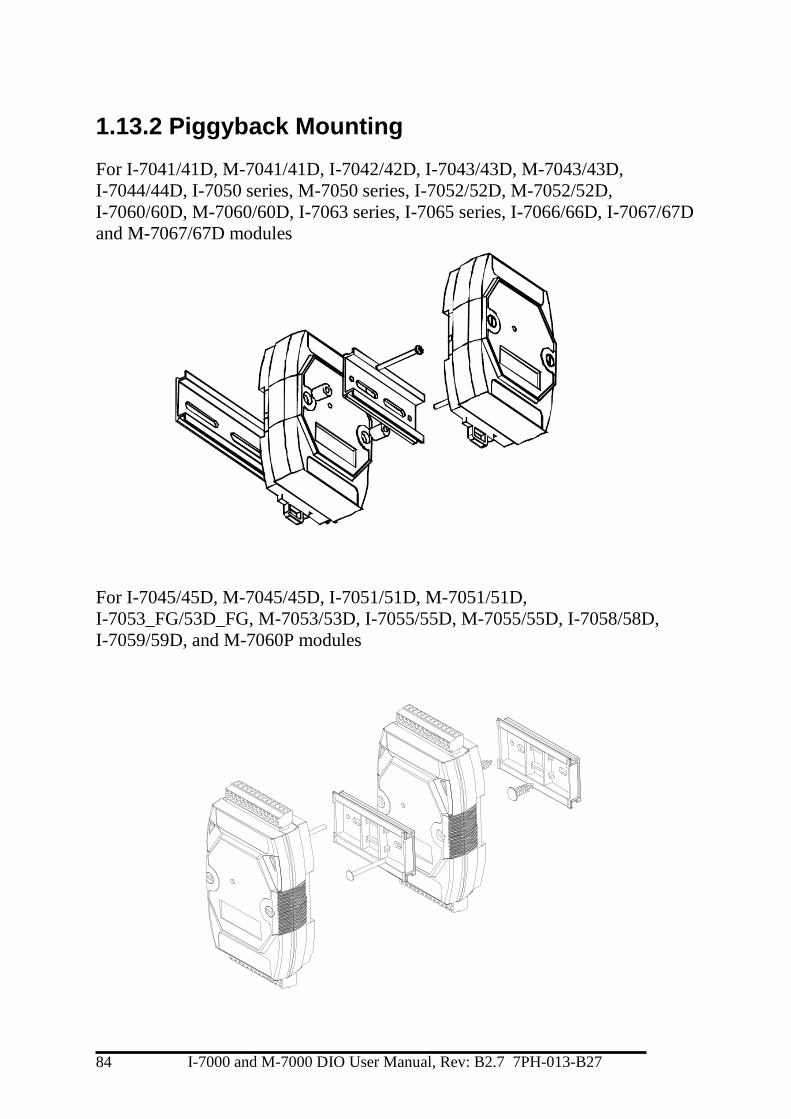
1.13.2 Piggyback Mounting ................................................... 84
1.13.3 Wall Mounting ............................................................ 85
1.14 Technical Support ................................................................ 86
2. DCON Protocol .............................................................................. 87
2.1 %AANNTTCCFF .................................................................. 90
2.2 #** .......................................................................................... 93
2.3 #AA00(Data) .......................................................................... 94
2.4 #AA0A(Data) ......................................................................... 96
2.5 #AA0B(Data) ......................................................................... 98
2.6 #AA1cDD ............................................................................. 100
2.7 #AAAcDD ............................................................................ 102
2.8 #AABcDD ............................................................................ 104
2.9 #AAN ................................................................................... 106
2.10 $AA2 .................................................................................. 108
2.11 $AA4 .................................................................................. 110
2.12 $AA5 .................................................................................. 112
2.13 $AA6 .................................................................................. 114
2.14 $AAC .................................................................................. 116
2.15 $AACN ............................................................................... 118
2.16 $AAF .................................................................................. 120
2.17 $AALS ................................................................................ 121
2.18 $AAM ................................................................................. 123
2.19 $AAP .................................................................................. 124
I-7000 and M-7000 DIO User Manual, Rev: B2.7 7PH-013-B27 5
2.20 $AAPN ............................................................................... 126
2.21 @AA ................................................................................... 128
2.22 @AA(Data) ........................................................................ 130
2.23 ~AAO(Name) ..................................................................... 132
2.24 ~** ...................................................................................... 134
2.25 ~AA0 .................................................................................. 135
2.26 ~AA1 .................................................................................. 137
2.27 ~AA2 .................................................................................. 139
2.28 ~AA3EVV .......................................................................... 141
2.29 ~AA4V ............................................................................... 143
2.30 ~AA5V ............................................................................... 145
2.31 ~AAD ................................................................................. 147
2.32 ~AADVV ........................................................................... 149
3. Modbus RTU Protocol ................................................................. 151
3.1 01 (0x01) Read Coils............................................................ 152
3.2 02 (0x02) Read Discrete Inputs ........................................... 156
3.3 03 (0x03) Read Multiple Registers ...................................... 158
3.4 04 (0x04) Read Multiple Input Registers ............................. 160
3.5 05 (0x05) Write Single Coils ............................................... 162
3.6 15 (0x0F) Write Multiple Coils ........................................... 165
3.7 70 (0x46) Read/Write Module Settings ............................... 168
3.7.1 Sub-function 00 (0x00) Read module name ............... 169
3.7.2 Sub-function 04 (0x04) Set module address ............... 170
3.7.3 Sub-function 05 (0x05) Read communication settings
.............................................................................................. 171
3.7.4 Sub-function 06 (0x06) Set communication settings.. 172
3.7.5 Sub-function 32 (0x20) Read firmware version ......... 174
3.7.6 Sub-function 33 (0x21) Set digital input counter trigger
edge ....................................................................................... 175
3.7.7 Sub-function 34 (0x22) Read digital input counter
trigger edge value ................................................................. 176
3.7.8 Sub-function 39 (0x27) Set the power-on value ......... 177
3.7.9 Sub-function 40 (0x28) Read the power-on value ...... 178
3.7.10 Sub-function 41 (0x29) Set DI/O active states ......... 179
3.7.11 Sub-function 42 (0x2A) Read DI/O active states ..... 181
3.8 Modbus Address Mapping ................................................... 182
4. Troubleshooting ............................................................................ 184
4.1 Communicating with the module ......................................... 185
I-7000 and M-7000 DIO User Manual, Rev: B2.7 7PH-013-B27 6
A. Appendix ..................................................................................... 186
A.1 INIT Mode ........................................................................... 186
A.2 Dual Watchdog Operation ................................................... 188
A.3 Frame Ground ...................................................................... 189
A.4 Reset Status ......................................................................... 191
A.5 Safe Value and Power-on Value of Digital Output ............ 192
A.6 Latched Digital Input ........................................................... 193
A.7 DN Module .......................................................................... 194
A.7.1 DN-SSR4 .................................................................... 195
A.7.2 DN-PR4 ...................................................................... 196
A.7.3 RM-104, RM-108, and RM-116 ................................ 197
A.7.4 RM-204, RM-208, RM-216 ....................................... 198
I-7000 and M-7000 DIO User Manual, Rev: B2.7 7PH-013-B27 7
1. Introduction
The I-7000 series is a family of network data acquisition and
control modules, providing analog-to-digital, digital-to-analog,
digital input/output, timer/counter and other functions. The
modules can be remotely controlled using a set of commands,
which we call the DCON protocol. Communication between
the module and the host is in ASCII format via an RS-485 bi-
directional serial bus standard. Baud Rates are software
programmable and transmission speeds of up to 115.2 Kbps
can be selected.
The functionality of the M-7000 series is the same as the I-
7000 series, with the exception that the M-7000 series offers
extended support for the Modbus RTU protocol.
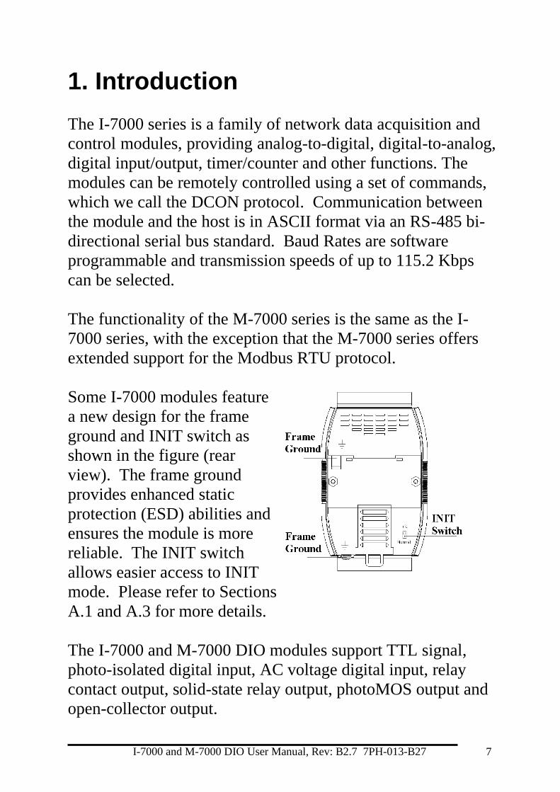
Some I-7000 modules feature
a new design for the frame
ground and INIT switch as
shown in the figure (rear
view). The frame ground
provides enhanced static
protection (ESD) abilities and
ensures the module is more
reliable. The INIT switch
allows easier access to INIT
mode. Please refer to Sections
A.1 and A.3 for more details.
The I-7000 and M-7000 DIO modules support TTL signal,
photo-isolated digital input, AC voltage digital input, relay
contact output, solid-state relay output, photoMOS output and
open-collector output.

I-7000 and M-7000 DIO User Manual, Rev: B2.7 7PH-013-B27 8
1.1 More Information
For more information regarding the I-7000 series, please refer
to chapter 1 of the “I-7000 Bus Converter User’s Manual” as
shown below or visit the ICP DAS website
http://www.icpdas.com.
1.1 The 7000 Series Overview
1.2 Related Documentation for the 7000 Series
1.3 Common Features of the 7000 Series
1.4 The 7000 Series System Network Configuration
1.5 7000 Dimensions
For details of INIT mode operation, please refer to
Section A.1 INIT Mode.
For details of module watchdog and host watchdog,
please refer to Section A.2 Dual Watchdog Operation.
For details of ESD protection and grounding, please
refer to Section A.3 Frame Ground.
There is a way to check whether the module is reset,
please refer to Section A.4 Reset Status for details.
For details of the safe value and power-on value of the
digital output, please refer to Section A.5 Safe Value and
Power-on Value of Digital Output.
The module with digital inputs provides the latched
digital inputs, please refer to Section A.6 Latched Digital
Input for details.
For details of the I/O extension modules, please refer to
Section A.7 DN Module.

I-7000 and M-7000 DIO User Manual, Rev: B2.7 7PH-013-B27 9
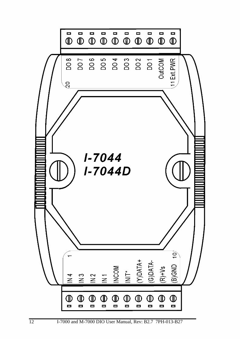
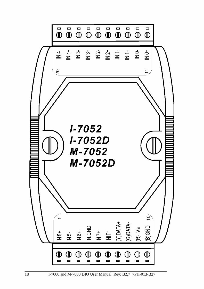
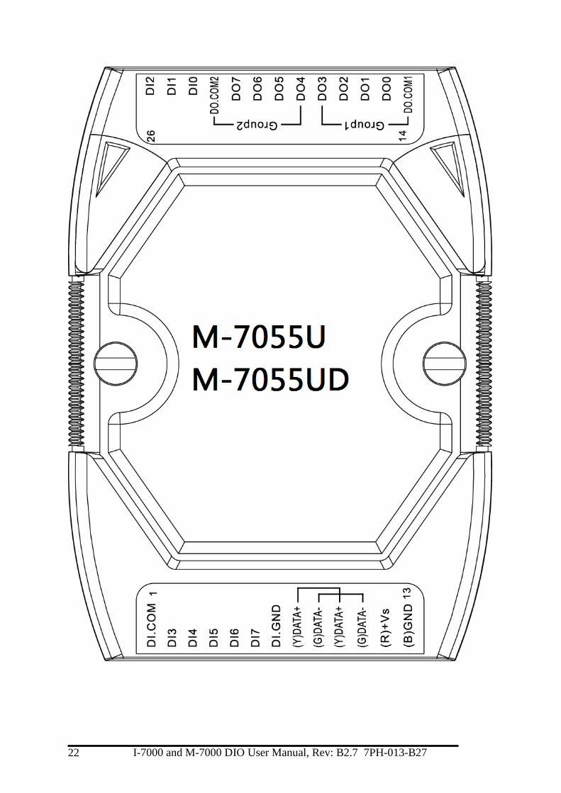
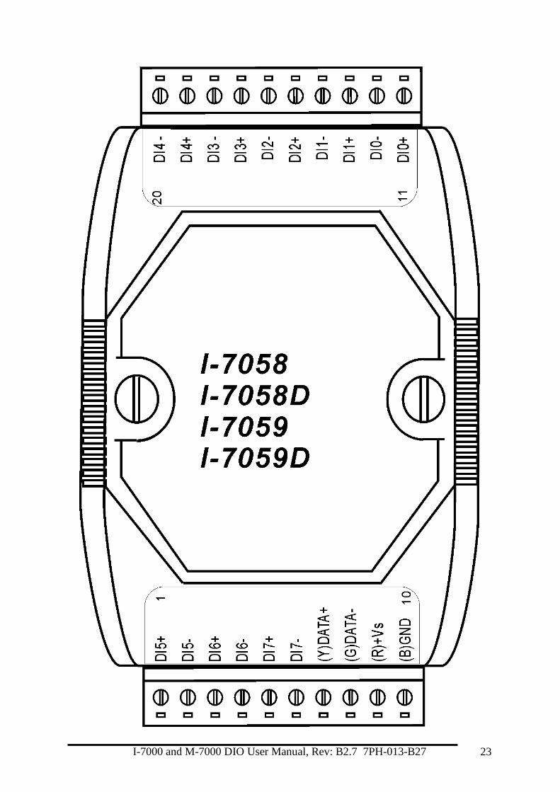
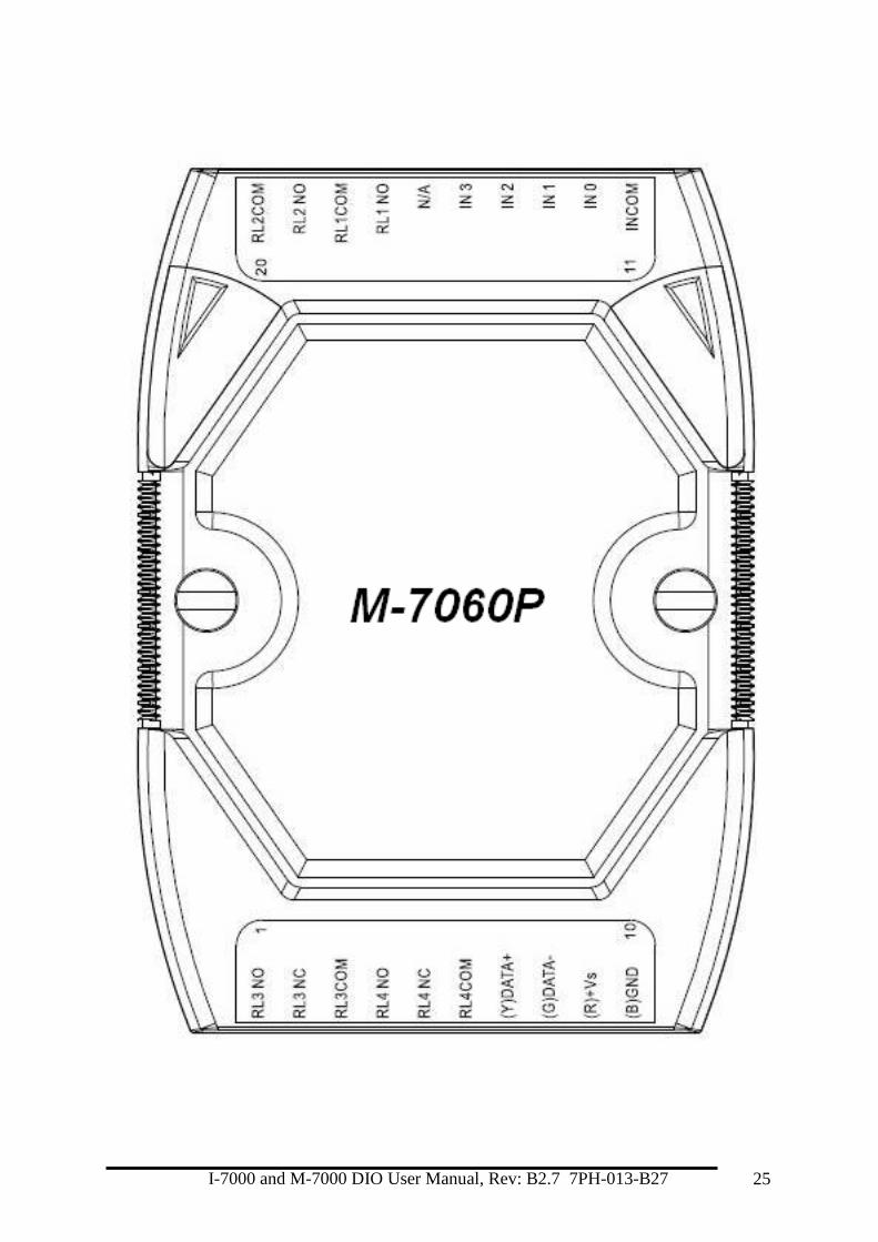
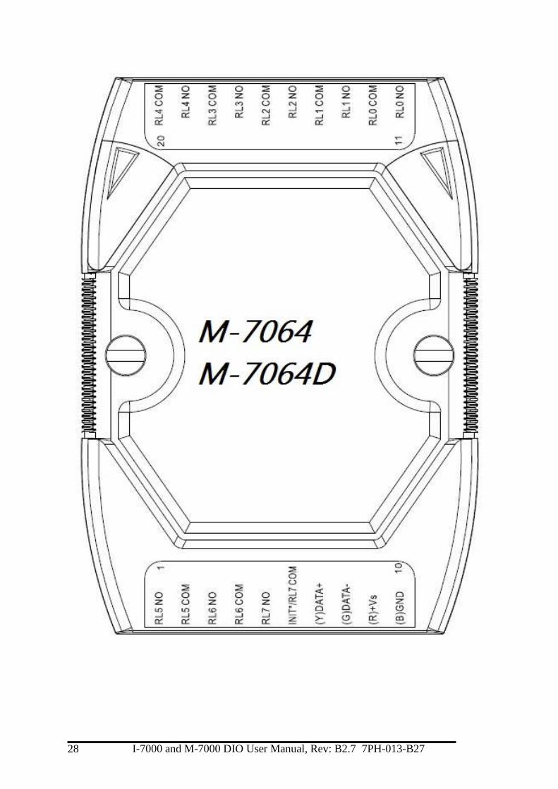
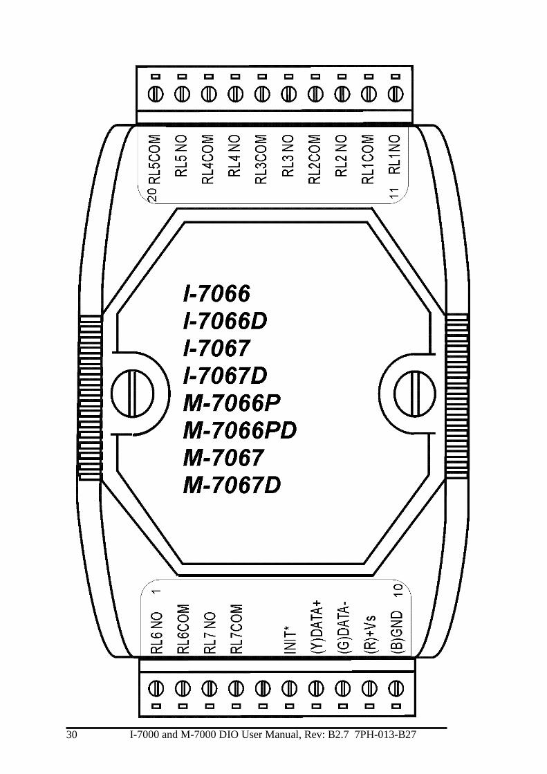
1.2 Terminal Assignment
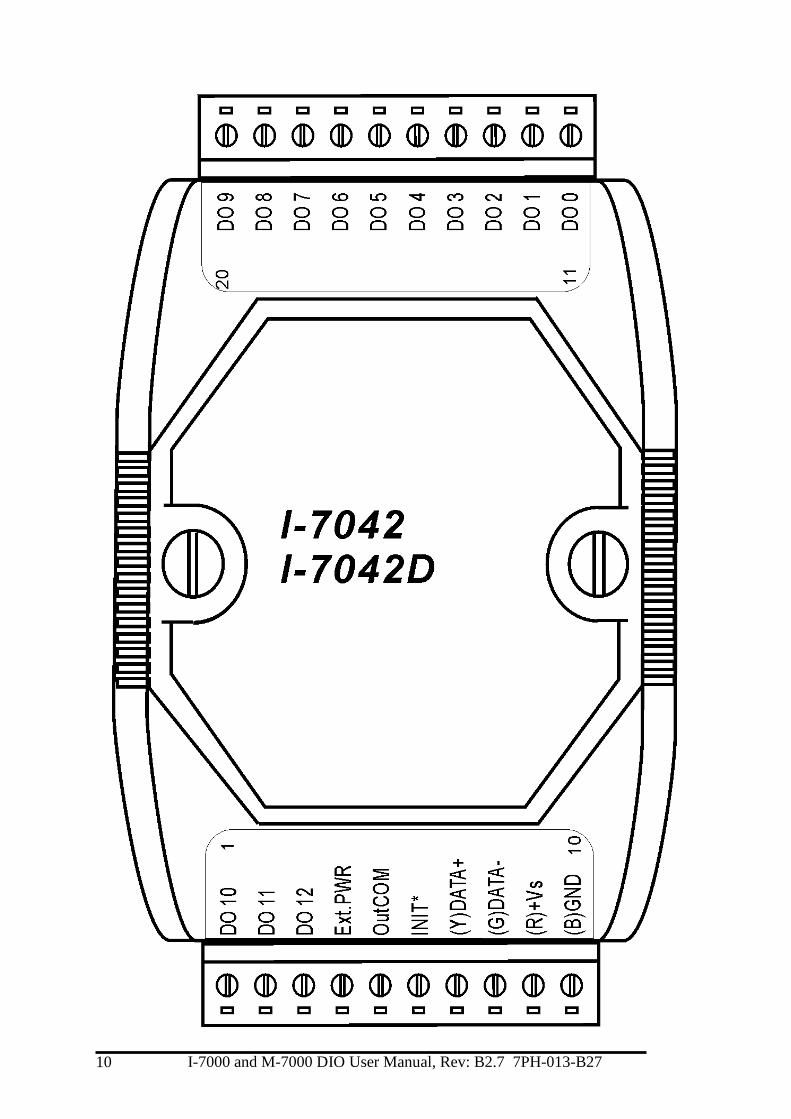
I-7000 and M-7000 DIO User Manual, Rev: B2.7 7PH-013-B27 10

I-7000 and M-7000 DIO User Manual, Rev: B2.7 7PH-013-B27 11
I-7000 and M-7000 DIO User Manual, Rev: B2.7 7PH-013-B27 12

I-7000 and M-7000 DIO User Manual, Rev: B2.7 7PH-013-B27 13
I-7000 and M-7000 DIO User Manual, Rev: B2.7 7PH-013-B27 14
I-7000 and M-7000 DIO User Manual, Rev: B2.7 7PH-013-B27 15
I-7000 and M-7000 DIO User Manual, Rev: B2.7 7PH-013-B27 16
I-7000 and M-7000 DIO User Manual, Rev: B2.7 7PH-013-B27 17
I-7000 and M-7000 DIO User Manual, Rev: B2.7 7PH-013-B27 18

I-7000 and M-7000 DIO User Manual, Rev: B2.7 7PH-013-B27 19

I-7000 and M-7000 DIO User Manual, Rev: B2.7 7PH-013-B27 20

I-7000 and M-7000 DIO User Manual, Rev: B2.7 7PH-013-B27 21
I-7000 and M-7000 DIO User Manual, Rev: B2.7 7PH-013-B27 22
I-7000 and M-7000 DIO User Manual, Rev: B2.7 7PH-013-B27 23

I-7000 and M-7000 DIO User Manual, Rev: B2.7 7PH-013-B27 24
I-7000 and M-7000 DIO User Manual, Rev: B2.7 7PH-013-B27 25

I-7000 and M-7000 DIO User Manual, Rev: B2.7 7PH-013-B27 26
I-7000 and M-7000 DIO User Manual, Rev: B2.7 7PH-013-B27 27
I-7000 and M-7000 DIO User Manual, Rev: B2.7 7PH-013-B27 28

I-7000 and M-7000 DIO User Manual, Rev: B2.7 7PH-013-B27 29
I-7000 and M-7000 DIO User Manual, Rev: B2.7 7PH-013-B27 30

I-7000 and M-7000 DIO User Manual, Rev: B2.7 7PH-013-B27 31
M-7068/M-7068D/M-7069/M-7069D

I-7000 and M-7000 DIO User Manual, Rev: B2.7 7PH-013-B27 32
1.3 Specifications
DC Input Modules
Module I-7041/41D
M-7041/41D
I-7041P/41PD
M-7041P/41PD
I-7051/51D
M-7051/51D
I-7052/52D
M-7052/52D
I-7053_FG/53D_FG
M-7053/53D
Input Channels 14
(Sink/Source) 14
(Sink/Source) 16 (Sink/Source) 8 (Sink) 16 (Source)
Input Type Isolated with
Common Power or Ground
Isolated with Common Power
or Ground
Dry Contact and Wet Contact
6 Differential and 2 Common Ground
Non-Isolated with Dry Contact
ON Voltage Level
+4 to +30 V +19 to +30 V +10 to +50 V +4 to +30 V Close to GND
OFF Voltage Level
+1 V Max. +1 V Max. +4 V Max. +1 V Max. open
Input Impedance
3K Ohms 3K Ohms 10K Ohms 3K Ohms 820 Ohms
Isolation Voltage
3750 Vrms 3750 Vrms 3750 Vrms 5000 Vrms Non-Isolated
Modbus RTU M-7041/41D M-7041P/41PD M-7051/51D M-7052/52D M-7053/53D
Power Requirement
+10 to +30 VDC
Power
Consumption
0.2 W for I-7041/ M-7041
0.9 W for I-7041D/ M-7041D
0.2 W for I-7041P/ M-7041P
0.9 W for I-7041PD/ M-7041PD
0.3 W for I-7051/ M-7051
1.1 W for I-7051D/ M-7051D
0.2 W for I-7052/ M-7052D
0.6 W for I-7052D/ M-7052D
0.6 W for I-7053/ M-7053
1.4 W for I-7053D/ M-7053D
Operating Temperature
-25 °C to +75 °C -25 °C to +75 °C -25 °C to +75 °C -25 °C to +75 °C -25 °C to +75 °C
Storage Temperature
-30 °C to +75 °C -30 °C to +75 °C -30 °C to +75 °C -30 °C to +75 °C -30 °C to +75 °C
I-7000 and M-7000 DIO User Manual, Rev: B2.7 7PH-013-B27 33
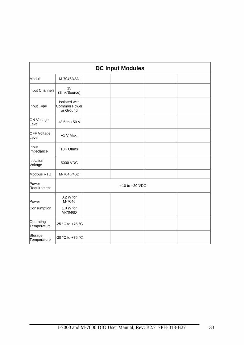
DC Input Modules
Module M-7046/46D
Input Channels 15
(Sink/Source)
Input Type Isolated with
Common Power or Ground
ON Voltage Level
+3.5 to +50 V
OFF Voltage Level
+1 V Max.
Input Impedance
10K Ohms
Isolation Voltage
5000 VDC
Modbus RTU M-7046/46D
Power Requirement
+10 to +30 VDC
Power
Consumption
0.2 W for M-7046
1.0 W for M-7046D
Operating Temperature
-25 °C to +75 °C
Storage Temperature
-30 °C to +75 °C
I-7000 and M-7000 DIO User Manual, Rev: B2.7 7PH-013-B27 34
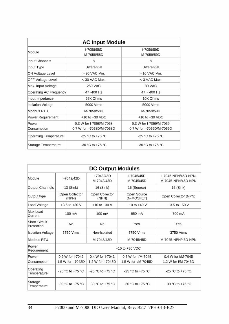
AC Input Module
Module I-7058/58D
M-7058/58D
I-7059/59D
M-7059/59D
Input Channels 8 8
Input Type Differential Differential
ON Voltage Level > 80 VAC Min. > 10 VAC Min.
OFF Voltage Level < 30 VAC Max. < 3 VAC Max.
Max. Input Voltage 250 VAC 80 VAC
Operating AC Frequency 47~400 Hz 47 ~ 400 Hz
Input Impedance 68K Ohms 10K Ohms
Isolation Voltage 5000 Vrms 5000 Vrms
Modbus RTU M-7058/58D M-7059/59D
Power Requirement +10 to +30 VDC +10 to +30 VDC
Power
Consumption
0.3 W for I-7058/M-7058
0.7 W for I-7058D/M-7058D
0.3 W for I-7059/M-7059
0.7 W for I-7059D/M-7059D
Operating Temperature -25 °C to +75 °C -25 °C to +75 °C
Storage Temperature -30 °C to +75 °C -30 °C to +75 °C
DC Output Modules
Module I-7042/42D I-7043/43D
M-7043/43D
I-7045/45D
M-7045/45D
I-7045-NPN/45D-NPN
M-7045-NPN/45D-NPN
Output Channels 13 (Sink) 16 (Sink) 16 (Source) 16 (Sink)
Output type Open Collector
(NPN) Open Collector
(NPN) Open Source (N-MOSFET)
Open Collector (NPN)
Load Voltage +3.5 to +30 V +10 to +30 V +10 to +40 V +3.5 to +50 V
Max Load Current
100 mA 100 mA 650 mA 700 mA
Short-Circuit Protection
No No Yes Yes
Isolation Voltage 3750 Vrms Non-Isolated 3750 Vrms 3750 Vrms
Modbus RTU M-7043/43D M-7045/45D M-7045-NPN/45D-NPN
Power Requirement
+10 to +30 VDC
Power
Consumption
0.9 W for I-7042
1.5 W for I-7042D
0.4 W for I-7043
1.2 W for I-7043D
0.6 W for I/M-7045
1.5 W for I/M-7045D
0.4 W for I/M-7045
1.2 W for I/M-7045D
Operating Temperature
-25 °C to +75 °C -25 °C to +75 °C -25 °C to +75 °C -25 °C to +75 °C
Storage Temperature
-30 °C to +75 °C -30 °C to +75 °C -30 °C to +75 °C -30 °C to +75 °C

I-7000 and M-7000 DIO User Manual, Rev: B2.7 7PH-013-B27 35
DC Input and Output Modules
Module I-7044/44D I-7050/50D I-7050A/50AD I-7055/55D
M-7055/55D
I-7055-NPN
I-7055D-NPN
M-7055-NPN
M-7055D-NPN
Output Channels
8 (Sink) 8 (Sink) 8 (Source) 8 (Source) 8 (Sink)
Output Type Open Collector
(NPN) Open Collector
(NPN) Open Collector
(PNP) Open Source (N-
MOSFET) Open Collector
(NPN)
Load Voltage +3.5 to +30 V +3.5 to +30 V +3.5 to +30 V +10 to +40 V +3.5 to +50 V
Max Load Current
375 mA 30 mA 50 mA 650 mA 700 mA
Short-Circuit Protection
No No No Yes Yes
Isolation Voltage
3750 Vrms Non-Isolated Non-Isolated 3750 Vrms 3750 Vrms
Input Channels 4 (Sink/Source) 7 (Source) 7 (Sink) 8 (Sink/Source) 8 (Sink/Source)
Input Type Isolated with
Common Source Non-Isolated Non-Isolated
Dry Contact and Wet Contact
Dry Contact and Wet Contact
ON Voltage Level
+4 to +30 V +4 to +30 V +4 to +30 V +10 to +50 V +10 to +50 V
OFF Voltage Level
+1 V Max. +1 V Max. +1 V Max. +4 V Max. +4 V Max.
Input Impedance
3K Ohms - - 10K Ohms 10K Ohms
Isolation Voltage
3750 Vrms Non-Isolated Non-Isolated 3750 Vrms 3750 Vrms
Modbus RTU M-7055/55D M-7055-NPN
M-7055D-NPN
Power Requirement
+10 to +30 V
Power
Consumption
0.6 W for I-7044
1.2 W for I-7044D
0.4 W for I-7050
1.2 W for I-7050D
1.0 W for I-7050A
1.8 W for I-7050AD
0.8 W for I-7055/ M-7055
1.6 W for I-7055D/
M-7055D
1.2 W for I-7055-NPN/ M-7055-NPN
2.2 W for I-7055D-NPN/ M-7055D-NPN
Operating Temperature
-25 °C to +75 °C -25 °C to +75 °C -25 °C to +75 °C -25 °C to +75 °C -25 °C to +75 °C
Storage Temperature
-30 °C to +75 °C -30 °C to +75 °C -30 °C to +75 °C -30 °C to +75 °C -30 °C to +75 °C
I-7000 and M-7000 DIO User Manual, Rev: B2.7 7PH-013-B27 36
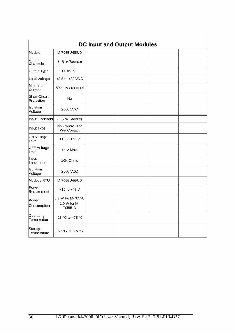
DC Input and Output Modules
Module M-7055U/55UD
Output Channels
8 (Sink/Source)
Output Type Push-Pull
Load Voltage +3.5 to +80 VDC
Max Load Current
500 mA / channel
Short-Circuit Protection
No
Isolation Voltage
2000 VDC
Input Channels 8 (Sink/Source)
Input Type Dry Contact and
Wet Contact
ON Voltage Level
+10 to +50 V
OFF Voltage Level
+4 V Max.
Input Impedance
10K Ohms
Isolation Voltage
2000 VDC
Modbus RTU M-7055U/55UD
Power Requirement
+10 to +48 V
Power
Consumption
0.9 W for M-7055U
1.0 W for M-7055UD
Operating Temperature
-25 °C to +75 °C
Storage Temperature
-30 °C to +75 °C

I-7000 and M-7000 DIO User Manual, Rev: B2.7 7PH-013-B27 37
Universal DC Input and Output Modules Model M-7054/54D M-7054P/54PD
Channels 16-channel Isolated Universal Digital Input / Output (Configurable via Wire Connection)
Digital Output Output Type Sink Sink
Load Voltage +5 ~ 30 VDC +5 ~ 50 VDC
Max Load Current 100 mA 500 mA
Overvoltage Protection 35V DC 60V DC
Overload Protection Yes
Short Circuit Protection Yes
Power-on Value Yes, Programmable Yes, Programmable
Safe Value Yes, Programmable Yes, Programmable
Digital Input ON Voltage Level Close to GND Close to GND
OFF Voltage Level Open Open
Overvoltage Protection 60 VDC
Isolation Voltage 3750 Vrms 3750 Vrms
Modbus RTU M-7054/54D M-7054P/54PD
Power Requirement +10 to +30 V
Power Consumption 1.2 W for M-7054
1.3 W for M-7054D 1.2 W for M-7054P
1.3 W for M-7054PD
Operating Temperature -25 °C to +75 °C
Storage Temperature -30 °C to +75 °C
I-7000 and M-7000 DIO User Manual, Rev: B2.7 7PH-013-B27 38
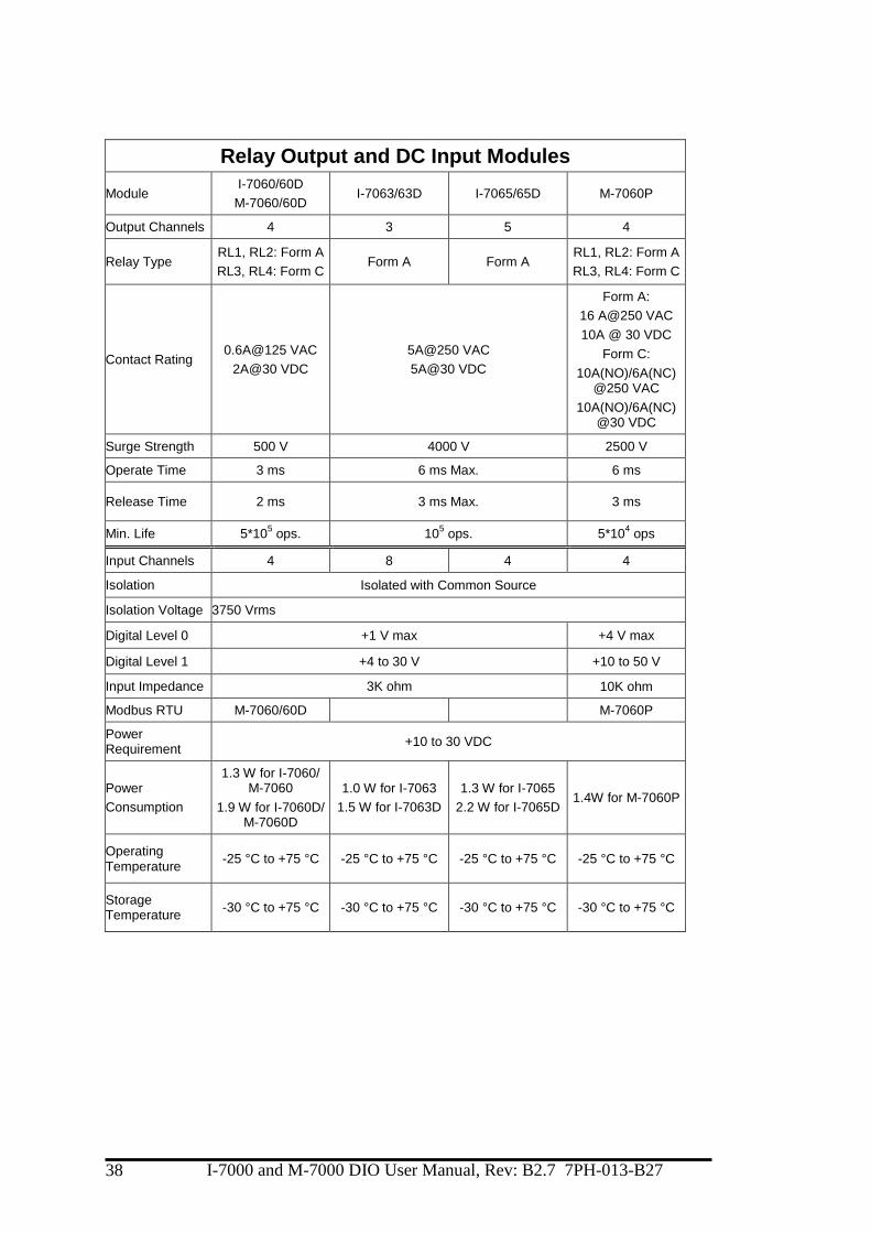
Relay Output and DC Input Modules
Module I-7060/60D
M-7060/60D I-7063/63D I-7065/65D M-7060P
Output Channels 4 3 5 4
Relay Type RL1, RL2: Form A RL3, RL4: Form C
Form A Form A RL1, RL2: Form A RL3, RL4: Form C
Contact Rating 0.6A@125 VAC
2A@30 VDC 5A@250 VAC 5A@30 VDC
Form A:
16 A@250 VAC
10A @ 30 VDC
Form C:
10A(NO)/6A(NC) @250 VAC
10A(NO)/6A(NC) @30 VDC
Surge Strength 500 V 4000 V 2500 V
Operate Time 3 ms 6 ms Max. 6 ms
Release Time 2 ms 3 ms Max. 3 ms
Min. Life 5*105 ops. 10
5 ops. 5*10
4 ops
Input Channels 4 8 4 4
Isolation Isolated with Common Source
Isolation Voltage 3750 Vrms
Digital Level 0 +1 V max +4 V max
Digital Level 1 +4 to 30 V +10 to 50 V
Input Impedance 3K ohm 10K ohm
Modbus RTU M-7060/60D M-7060P
Power Requirement +10 to 30 VDC
Power Consumption
1.3 W for I-7060/ M-7060
1.9 W for I-7060D/ M-7060D
1.0 W for I-7063 1.5 W for I-7063D
1.3 W for I-7065 2.2 W for I-7065D
1.4W for M-7060P
Operating Temperature
-25 °C to +75 °C -25 °C to +75 °C -25 °C to +75 °C -25 °C to +75 °C
Storage Temperature
-30 °C to +75 °C -30 °C to +75 °C -30 °C to +75 °C -30 °C to +75 °C

I-7000 and M-7000 DIO User Manual, Rev: B2.7 7PH-013-B27 39
Relay Output Modules
Module I-7067/67D
M-7067/67D
I-7061/61D
M-7061/61D M-7068/68D M-7069/69D
Output Channels 7 Form A 12 Form A 4 Form A, 4 Form C 4 Form A, 4 Form C
Relay Type Signal Relay Power Relay Signal Relay Power Relay
Contact Rating 0.5A@120 VAC
1.0A@24 VDC 5A@250 VAC 5A@30 VDC
2 A @ 30 VDC
0.24 A @ 220 VDC
0.25 A @ 250 VAC
Form A:
6 A @ 35 VDC
6 A @ 240 VAC
Form C:
5 A @ 30 VDC
5 A @ 250 VAC
Surge Strength 1500 VDC 3000 VDC 2000 VDC 4000 VDC
Operate Time 5 ms Max. 6 ms 3 ms (typical) 5 ms (typical)
Release Time 2 ms Max. 3 ms 4 ms (typical)
Form A:
1 ms (typical)
Form C:
2 ms (typical)
Min. Life 105 ops. 20x10
5 ops
108 ops.
Mechanical
2x10⁵ ops
Electrical
Form A:
30x106 ops.
Mechanical
105 ops
Electrical
Form C:
15x106 ops.
Mechanical
105 ops
Electrical
Modbus RTU M-7067/67D M-7061/61D M-7068/68D M-7069/69D
Power Requirement +10 to 30 VDC
Power Consumption
1.5W for I-7067/ M-7067
2.2 W for I-7067D/ M-7067D
1.7W for I-7061/ M-7061
2.3 W for I-7061D/ M-7061D
1.6 W for M-7068
2.0 W for M-7068D 2.1 W for M-7069
2.5 W for M-7069D
Operating Temperature
-25 °C to +75 °C
Storage Temperature
-30 °C to +75 °C

I-7000 and M-7000 DIO User Manual, Rev: B2.7 7PH-013-B27 40
Relay Output Modules
Module M-7064/64D
Output Channels 8 Form A
Relay Type Signal Relay
Contact Rating 0.25A@250 VAC
2.0A@30 VDC
Surge Strength 2000 VDC
Operate Time 3 ms (typical)
Release Time 4 ms (typical)
Min. Life 108 ops.
Modbus RTU M-7064/64D
Power Requirement +10 to 30 VDC
Power Consumption
1.5W for M-7064
1.9 W for M-7064D
Operating Temperature
-25 °C to +75 °C
Storage Temperature
-30 °C to +75 °C
I-7000 and M-7000 DIO User Manual, Rev: B2.7 7PH-013-B27 41
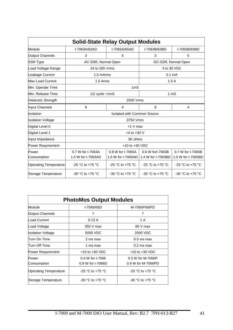
Solid-State Relay Output Modules
Module I-7063A/63AD I-7065A/65AD I-7063B/63BD I-7065B/65BD
Output Channels 3 5 3 5
SSR Type AC-SSR, Normal Open DC-SSR, Normal Open
Load Voltage Range 24 to 265 Vrms 3 to 30 VDC
Leakage Current 1.5 mArms 0.1 mA
Max Load Current 1.0 Arms 1.0 A
Min. Operate Time 1mS
Min. Release Time 1/2 cycle +1mS 1 mS
Dielectric Strength 2500 Vrms
Input Channels 8 4 8 4
Isolation Isolated with Common Source
Isolation Voltage 3750 Vrms
Digital Level 0 +1 V max
Digital Level 1 +4 to +30 V
Input Impedance 3K ohms
Power Requirement +10 to +30 VDC
Power Consumption
0.7 W for I-7063A 1.5 W for I-7063AD
0.8 W for I-7065A 1.6 W for I-7065AD
0.6 W forI-7063B 1.4 W for I-7063BD
0.7 W for I-7065B 1.5 W for I-7065BD
Operating Temperature -25 °C to +75 °C -25 °C to +75 °C -25 °C to +75 °C -25 °C to +75 °C
Storage Temperature -30 °C to +75 °C -30 °C to +75 °C -30 °C to +75 °C -30 °C to +75 °C
PhotoMos Output Modules
Module I-7066/66D M-7066P/66PD
Output Channels 7 7
Load Current 0.13 A 1 A
Load Voltage 350 V max 80 V max
Isolation Voltage 5000 VDC 2000 VDC
Turn On Time 2 ms max 0.5 ms max
Turn Off Time 1 ms max 0.2 ms max
Power Requirement +10 to +30 VDC +10 to +30 VDC
Power Consumption
0.4 W for I-7066 0.8 W for I-7066D
0.5 W for M-7066P 0.9 W for M-7066PD
Operating Temperature -25 °C to +75 °C -25 °C to +75 °C
Storage Temperature -30 °C to +75 °C -30 °C to +75 °C

I-7000 and M-7000 DIO User Manual, Rev: B2.7 7PH-013-B27 42
1.4 Block Diagrams
1.4.1 Block Diagram for the I-7041/41D, I-7041P/41PD, M-7041/41D and M-7041P/41PD
1.4.2 Block Diagram for the I-7042/42D
I-7000 and M-7000 DIO User Manual, Rev: B2.7 7PH-013-B27 43
1.4.3 Block Diagram for the I-7043/43D and M-7043/43D
1.4.4 Block Diagram for the I-7044/44D
I-7000 and M-7000 DIO User Manual, Rev: B2.7 7PH-013-B27 44
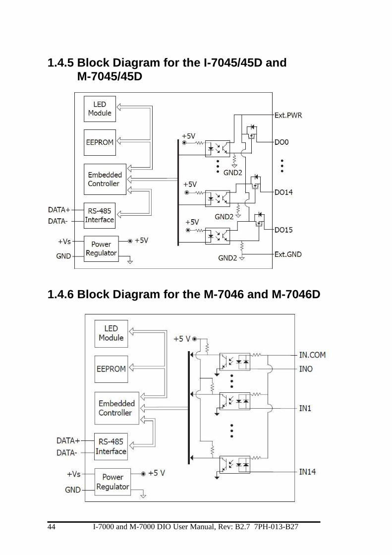
1.4.5 Block Diagram for the I-7045/45D and M-7045/45D
1.4.6 Block Diagram for the M-7046 and M-7046D

I-7000 and M-7000 DIO User Manual, Rev: B2.7 7PH-013-B27 45
1.4.7 Block Diagram for the I-7045-NPN/45D-NPN and M-7045-NPN/45D-NPN
1.4.8 Block Diagram for the I-7050/50D and M-7050/50D
I-7000 and M-7000 DIO User Manual, Rev: B2.7 7PH-013-B27 46
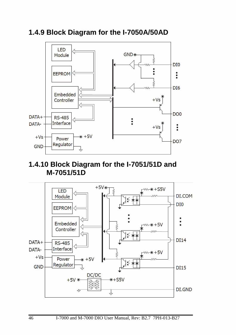
1.4.9 Block Diagram for the I-7050A/50AD
1.4.10 Block Diagram for the I-7051/51D and M-7051/51D
I-7000 and M-7000 DIO User Manual, Rev: B2.7 7PH-013-B27 47
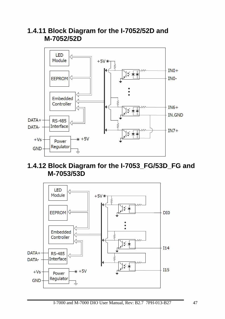
1.4.11 Block Diagram for the I-7052/52D and M-7052/52D
1.4.12 Block Diagram for the I-7053_FG/53D_FG and M-7053/53D
I-7000 and M-7000 DIO User Manual, Rev: B2.7 7PH-013-B27 48
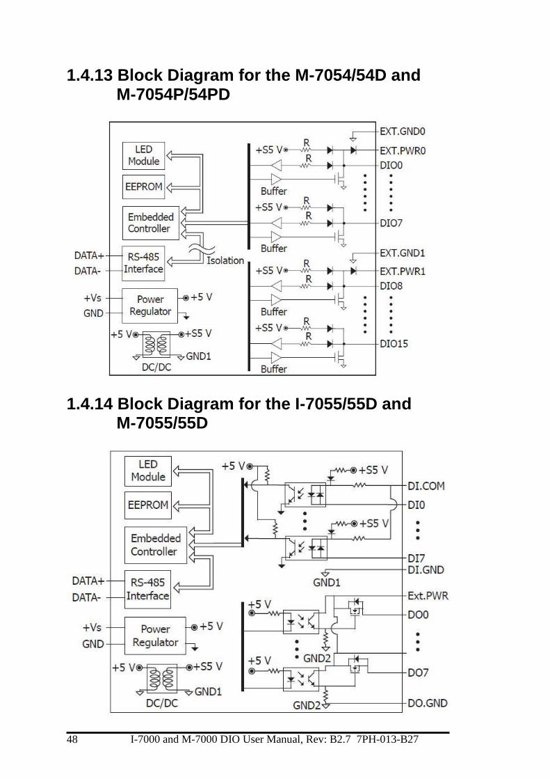
1.4.13 Block Diagram for the M-7054/54D and M-7054P/54PD
1.4.14 Block Diagram for the I-7055/55D and M-7055/55D
I-7000 and M-7000 DIO User Manual, Rev: B2.7 7PH-013-B27 49
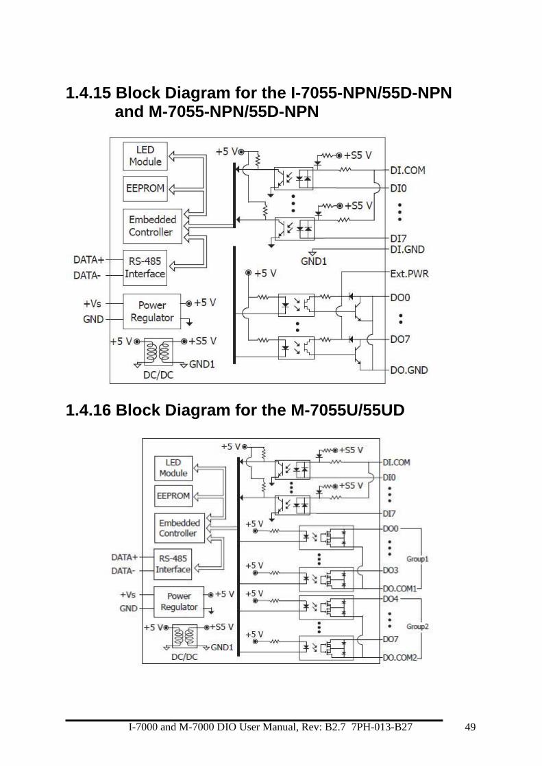
1.4.15 Block Diagram for the I-7055-NPN/55D-NPN
and M-7055-NPN/55D-NPN
1.4.16 Block Diagram for the M-7055U/55UD

I-7000 and M-7000 DIO User Manual, Rev: B2.7 7PH-013-B27 50
1.4.17 Block Diagram for the I-7058/58D and M-7058/58D
1.4.18 Block Diagram for the I-7059/59D and M-7059/59D

I-7000 and M-7000 DIO User Manual, Rev: B2.7 7PH-013-B27 51
1.4.19 Block Diagram for the I-7060/60D, M-7060/60D, and M-7060P
1.4.20 Block Diagram for the I-7061/61D and M-7061/61D

I-7000 and M-7000 DIO User Manual, Rev: B2.7 7PH-013-B27 52
1.4.21 Block Diagram for the I-7063/63D
1.4.22 Block Diagram for the I-7063A/63AD

I-7000 and M-7000 DIO User Manual, Rev: B2.7 7PH-013-B27 53
1.4.23 Block Diagram for the I-7063B/63BD
I-7000 and M-7000 DIO User Manual, Rev: B2.7 7PH-013-B27 54
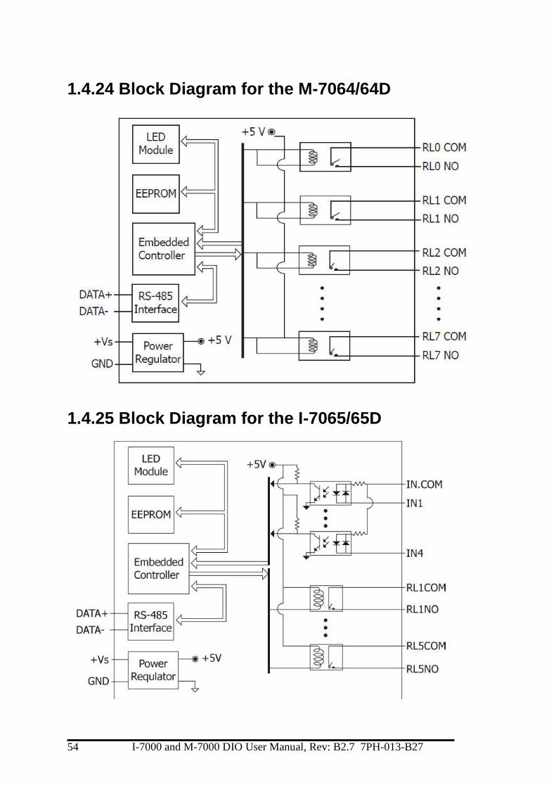
1.4.24 Block Diagram for the M-7064/64D
1.4.25 Block Diagram for the I-7065/65D
I-7000 and M-7000 DIO User Manual, Rev: B2.7 7PH-013-B27 55
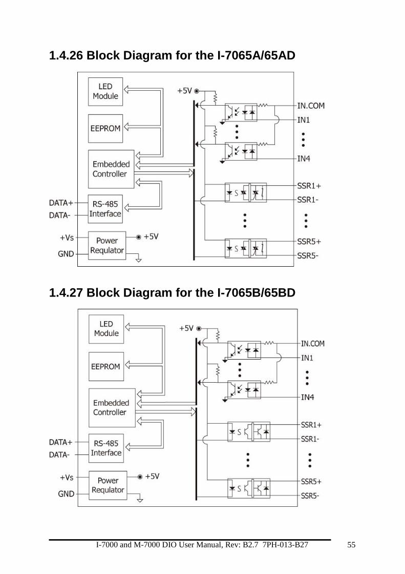
1.4.26 Block Diagram for the I-7065A/65AD
1.4.27 Block Diagram for the I-7065B/65BD

I-7000 and M-7000 DIO User Manual, Rev: B2.7 7PH-013-B27 56
1.4.28 Block Diagram for the I-7066/66D and M-7066P/66PD
1.4.29 Block Diagram for the I-7067/67D and M-7067/67D

I-7000 and M-7000 DIO User Manual, Rev: B2.7 7PH-013-B27 57
1.4.30 Block Diagram for the M-7068/68D and M-7069/69D
I-7000 and M-7000 DIO User Manual, Rev: B2.7 7PH-013-B27 58
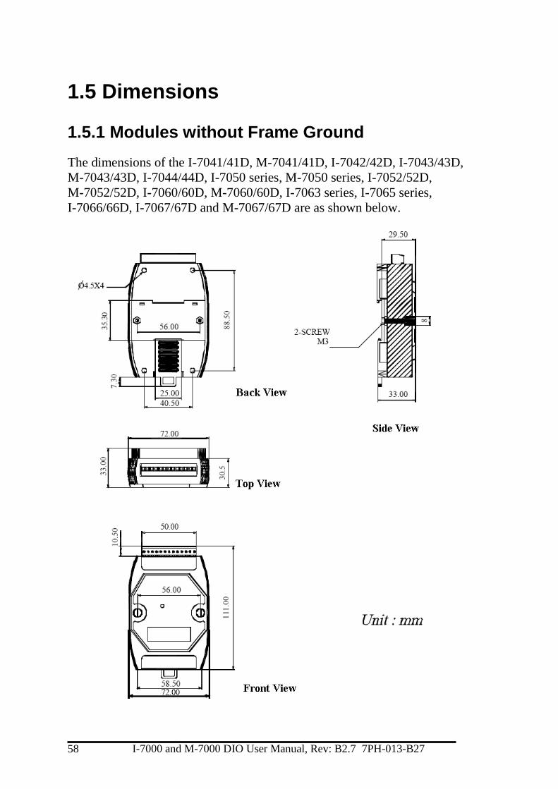
1.5 Dimensions 1.5.1 Modules without Frame Ground
The dimensions of the I-7041/41D, M-7041/41D, I-7042/42D, I-7043/43D,
M-7043/43D, I-7044/44D, I-7050 series, M-7050 series, I-7052/52D,
M-7052/52D, I-7060/60D, M-7060/60D, I-7063 series, I-7065 series,
I-7066/66D, I-7067/67D and M-7067/67D are as shown below.
I-7000 and M-7000 DIO User Manual, Rev: B2.7 7PH-013-B27 59
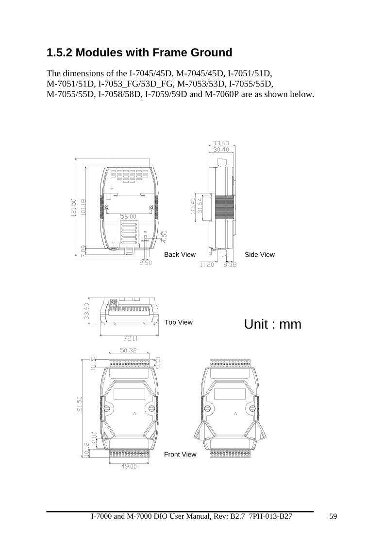
1.5.2 Modules with Frame Ground
The dimensions of the I-7045/45D, M-7045/45D, I-7051/51D,
M-7051/51D, I-7053_FG/53D_FG, M-7053/53D, I-7055/55D,
M-7055/55D, I-7058/58D, I-7059/59D and M-7060P are as shown below.
Back View
Top View
Front View
Side View
Unit : mm
lnit
Normal

I-7000 and M-7000 DIO User Manual, Rev: B2.7 7PH-013-B27 60
1.6 Wiring 1.6.1 I-7041/41D, I-7041P/41PD, M-7041/41D and
M-7041P/41PD wiring
Dry Contact
TTL/CMOS
NPN Output PNP Output
1.6.2 I-7042/42D wiring
Open Collector Output
1.6.3 I-7043/43D and M-7043/43D wiring
Open Collector Output

I-7000 and M-7000 DIO User Manual, Rev: B2.7 7PH-013-B27 61
1.6.4 I-7044/44D wiring
Input
Wiring
Dry Contact
TTL/CMOS
NPN Output PNP Output
Output Wiring
Open Collector
1.6.5 I-7045/45D and M-7045/45D wiring
Digital Output

I-7000 and M-7000 DIO User Manual, Rev: B2.7 7PH-013-B27 62
1.6.6 I-7045-NPN, I-7045D-NPN, M-7045-NPN and M-7045D-NPN wiring
1.6.7 M-7046/46D wiring
I-7000 and M-7000 DIO User Manual, Rev: B2.7 7PH-013-B27 63
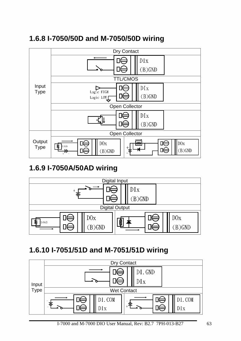
1.6.8 I-7050/50D and M-7050/50D wiring
Input Type
Dry Contact
TTL/CMOS
Open Collector
Output Type
Open Collector
1.6.9 I-7050A/50AD wiring
Digital Input
Digital Output
1.6.10 I-7051/51D and M-7051/51D wiring
Input Type
Dry Contact
Wet Contact

I-7000 and M-7000 DIO User Manual, Rev: B2.7 7PH-013-B27 64
1.6.11 I-7052/52D and M-7052/52D wiring
Input Type
Wet Contact
TTL/CMOS
NPN Output PNP Output
1.6.12 I-7053_FG/53D_FG and M-7053/53D wiring
Input
Type
Dry Contact
TTL/CMOS
Open Collector
I-7000 and M-7000 DIO User Manual, Rev: B2.7 7PH-013-B27 65
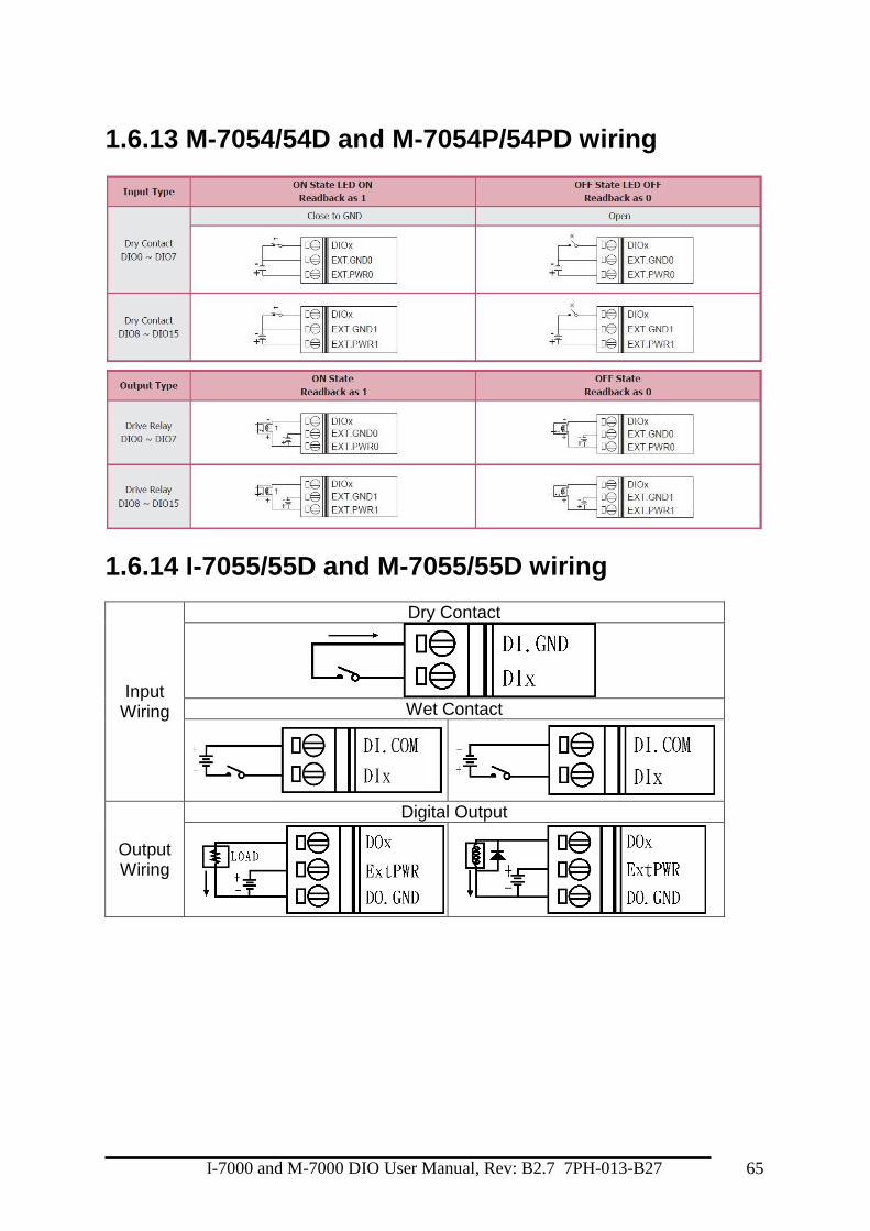
1.6.13 M-7054/54D and M-7054P/54PD wiring
1.6.14 I-7055/55D and M-7055/55D wiring
Input Wiring
Dry Contact
Wet Contact
Output Wiring
Digital Output

I-7000 and M-7000 DIO User Manual, Rev: B2.7 7PH-013-B27 66
1.6.15 I-7055-NPN, I-7055D-NPN, M-7055-NPN and M-7055D-NPN wiring
Input
Type
Dry Contact
Wet Contact
Output
Type
ON State LED ON
Readback as 1
OFF State LED OFF
Readback as 0
Relay ON Relay Off
Drive
Relay
Resistance
Load

I-7000 and M-7000 DIO User Manual, Rev: B2.7 7PH-013-B27 67
1.6.16 M-7055U/55UD

I-7000 and M-7000 DIO User Manual, Rev: B2.7 7PH-013-B27 68
1.6.17 I-7058/58D, I-7059/59D, M-7058/58D and M-7059/59D wiring
Digital Input
1.6.18 I-7060/60D and M-7060/60D wiring
Input
Wiring
Dry Contact
TTL/CMOS
NPN Output PNP Output
Output
Wiring
Relay Output in RL1 and RL2
Relay ON Relay OFF
Relay Output in RL3 and RL4
Relay ON Relay OFF
I-7000 and M-7000 DIO User Manual, Rev: B2.7 7PH-013-B27 69
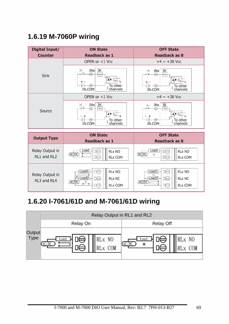
1.6.19 M-7060P wiring
1.6.20 I-7061/61D and M-7061/61D wiring
Output Type
Relay Output in RL1 and RL2
Relay On Relay Off

I-7000 and M-7000 DIO User Manual, Rev: B2.7 7PH-013-B27 70
1.6.21 I-7063/63D, I-7063A/63AD, I-7063B/63BD, I-7065/65D, I-7065A/65AD and I-7065B/65BD wiring
Input
Wiring
Dry Contact
TTL/CMOS
NPN Output PNP Output
Output
Wiring
Relay Output
Relay ON Relay OFF
1.6.22 M-7064/64D wiring

I-7000 and M-7000 DIO User Manual, Rev: B2.7 7PH-013-B27 71
1.6.23 I-7066/66D, I-7067/67D, M-7066P/66PD and M-7067/67D wiring
Relay Output
Relay ON Relay OFF
1.6.24 M-7068/68D and M-7069/69D wiring
1.6.25 Wiring Recommendations
Use 26-12 AWG wire for signal connections.
Strip the wire to a length of 7±0.5mm.
Use a crimp terminal for wiring.
Avoid high-voltage cables and power equipment as
much as possible.
For RS-485 communication, use insulated and twisted
pair 24 AWG wire, e.g. Belden 9841.

I-7000 and M-7000 DIO User Manual, Rev: B2.7 7PH-013-B27 72
1.7 Jumper Setting
Note: To access the jumper, the cover must be opened.
For the I-7043/43D and M-7043/43D modules, the INIT*
terminal is shared with the DO15 terminal. The functionality
of the terminal is set using the J3 jumper. The position of the
J3 jumper is shown in the figure below.
The settings for the J3 jumper are as follows.
Terminal INIT*/DO15 is set to INIT*. The
digital output channel 15 is disabled and
INIT mode is available. (factory default)
Terminal INIT*/DO15 is set to DO15. The
digital output channel 15 is enabled and
INIT mode is not available.
I-7000 and M-7000 DIO User Manual, Rev: B2.7 7PH-013-B27 73
1.8 Quick Start
To install the module, follow the steps below:
1. Refer to Section 1.2 for the terminal assignment and
Section 1.6 for the wiring diagram.
2. Connect the module to the RS-485 network using the
DATA+ and DATA- terminals. See Section 1.2 for the
terminal assignment. If the host is only equipped with an
RS-232 interface, then an RS-232 to RS-485 converter
will be required. Refer to the “I-7000 Bus Converter
User’s Manual” for more information.
3. Connect the module to the power supply using the +Vs
and GND terminals. See Section 1.2 for the terminal
assignment. Note that the voltage supplied to the module
should be in the range of +10 to +30 VDC.
4. Configure the module by sending the %AANNTTCCFF
command. See Section 2.1 for details. For M-7000
modules using the Modbus RTU protocol, configure the
module using the following functions.
Sub-function 04h of Function 46h, see Section 3.7.2
Sub-function 06h of Function 46h, see Section 3.7.4
The default settings for the module can be found in
Section 1.9.
5. To read data from the input channels, send either the
$AA6 or @AA commands to the module. See Sections
2.13 and 2.21 for details. For M-7000 modules using the
Modbus RTU protocol, use Function 02h to read the data
from the input channels. See Section 3.2 for details.
6. To write data to the output channels, send the @AA(data)
command to the module. See Section 2.22 for details.
Refer to Sections 2.3 ~ 2.8 for other setting digital output
commands. For M-7000 modules using the Modbus RTU
protocol, use Function 05h or 0Fh to write the data to the
output channels. See Sections 3.5 and 3.6 for details.

I-7000 and M-7000 DIO User Manual, Rev: B2.7 7PH-013-B27 74
7. If the host is a PC with a Windows operating system
installed, the DCON Utility can be used to allow easy
configuration and reading of data. The DCON Utility can
be downloaded from the ICP DAS website
(http://www.icpdas.com). The documentation for the
DCON Utility can be found in the ”Getting Started For
I-7000 Series Modules” manual.
Please refer to the “I-7000 Bus Converter User’s Manual”
and ”Getting Started For I-7000 Series Modules” manuals
for more details. The “Getting Started For I-7000 Series
Modules” manual can be downloaded from the ICP DAS
website (http://www.icpdas.com).
I-7000 and M-7000 DIO User Manual, Rev: B2.7 7PH-013-B27 75
1.9 Default Settings
Default settings for the I-7000 DIO modules are as follows:
。 Module Address: 01
。 DIO Type: Type 40
。 Baud Rate: 9600 bps
。 Checksum disabled
。 J3 set to INIT mode enabled for I-7043/43D and M-7043/43D.
Default settings for the M-7000 DIO modules are as follows:
。 Protocol: Modbus RTU
。 Module Address: 01
。 DIO Type: Type 40
。 Baud Rate: 9600 bps

I-7000 and M-7000 DIO User Manual, Rev: B2.7 7PH-013-B27 76
1.10 Configuration Tables
Baud Rate Setting (CC)
Code 03 04 05 06 07 08 09 0A
Baud rate 1200 2400 4800 9600 19200 38400 57600 115200
Note: The data bits are fixed at one start bit, eight data bits, no parity and one
stop bit for both the I-7000 and M-7000 series.
Type Setting (TT)
For I-7000 and M-7000 DIO modules, the type code is fixed
to 40.

I-7000 and M-7000 DIO User Manual, Rev: B2.7 7PH-013-B27 77
Data Format Setting (FF)
7 6 5 4 3 2 1 0
CU CS reserved CD
Key Description
CD Code
I-7050: 0 (read only)
I-7052: 2 (read only)
I-7053: 3 (read only)
I-7060: 1 (read only)
For other modules, the code value can be
changed by %AANNTTCCFF command and
the default code value is 0.
CS Checksum setting
0: Disabled
1: Enabled
CU Counter update
0: The counter is updated when there is a falling
edge in the input signal.
1: The counter is updated when there is a rising
edge in the input signal.
Note: The reserved bits should be zero.
I-7000 and M-7000 DIO User Manual, Rev: B2.7 7PH-013-B27 78
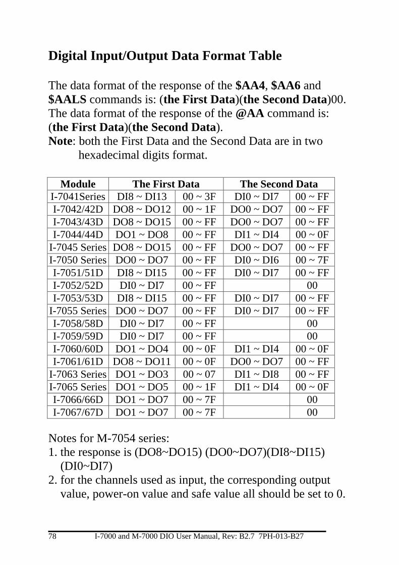
Digital Input/Output Data Format Table
The data format of the response of the $AA4, $AA6 and
$AALS commands is: (the First Data)(the Second Data)00.
The data format of the response of the @AA command is:
(the First Data)(the Second Data).
Note: both the First Data and the Second Data are in two
hexadecimal digits format.
Module The First Data The Second Data
I-7041Series DI8 ~ DI13 00 ~ 3F DI0 ~ DI7 00 ~ FF
I-7042/42D DO8 ~ DO12 00 ~ 1F DO0 ~ DO7 00 ~ FF
I-7043/43D DO8 ~ DO15 00 ~ FF DO0 ~ DO7 00 ~ FF
I-7044/44D DO1 ~ DO8 00 ~ FF DI1 ~ DI4 00 ~ 0F
I-7045 Series DO8 ~ DO15 00 ~ FF DO0 ~ DO7 00 ~ FF
I-7050 Series DO0 ~ DO7 00 ~ FF DI0 ~ DI6 00 ~ 7F
I-7051/51D DI8 ~ DI15 00 ~ FF DI0 ~ DI7 00 ~ FF
I-7052/52D DI0 ~ DI7 00 ~ FF 00
I-7053/53D DI8 ~ DI15 00 ~ FF DI0 ~ DI7 00 ~ FF
I-7055 Series DO0 ~ DO7 00 ~ FF DI0 ~ DI7 00 ~ FF
I-7058/58D DI0 ~ DI7 00 ~ FF 00
I-7059/59D DI0 ~ DI7 00 ~ FF 00
I-7060/60D DO1 ~ DO4 00 ~ 0F DI1 ~ DI4 00 ~ 0F
I-7061/61D DO8 ~ DO11 00 ~ 0F DO0 ~ DO7 00 ~ FF
I-7063 Series DO1 ~ DO3 00 ~ 07 DI1 ~ DI8 00 ~ FF
I-7065 Series DO1 ~ DO5 00 ~ 1F DI1 ~ DI4 00 ~ 0F
I-7066/66D DO1 ~ DO7 00 ~ 7F 00
I-7067/67D DO1 ~ DO7 00 ~ 7F 00
Notes for M-7054 series:
1. the response is (DO8~DO15) (DO0~DO7)(DI8~DI15)
(DI0~DI7)
2. for the channels used as input, the corresponding output
value, power-on value and safe value all should be set to 0.
I-7000 and M-7000 DIO User Manual, Rev: B2.7 7PH-013-B27 79
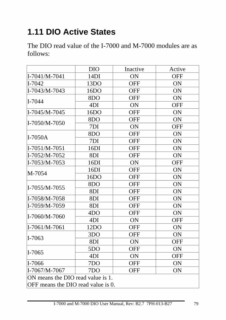
1.11 DIO Active States
The DIO read value of the I-7000 and M-7000 modules are as
follows:
DIO Inactive Active
I-7041/M-7041 14DI ON OFF
I-7042 13DO OFF ON
I-7043/M-7043 16DO OFF ON
I-7044 8DO OFF ON
4DI ON OFF
I-7045/M-7045 16DO OFF ON
I-7050/M-7050 8DO OFF ON
7DI ON OFF
I-7050A 8DO OFF ON
7DI OFF ON
I-7051/M-7051 16DI OFF ON
I-7052/M-7052 8DI OFF ON
I-7053/M-7053 16DI ON OFF
M-7054 16DI OFF ON
16DO OFF ON
I-7055/M-7055 8DO OFF ON
8DI OFF ON
I-7058/M-7058 8DI OFF ON
I-7059/M-7059 8DI OFF ON
I-7060/M-7060 4DO OFF ON
4DI ON OFF
I-7061/M-7061 12DO OFF ON
I-7063 3DO OFF ON
8DI ON OFF
I-7065 5DO OFF ON
4DI ON OFF
I-7066 7DO OFF ON
I-7067/M-7067 7DO OFF ON
ON means the DIO read value is 1.
OFF means the DIO read value is 0.
I-7000 and M-7000 DIO User Manual, Rev: B2.7 7PH-013-B27 80
1.12 M-7000 Notes
The main difference between the I-7000 and M-7000 series is
that the M-7000 series has additional support for the Modbus
RTU communication protocol, which is the default protocol
of the M-7000 series. The communication Baud Rates for the
Modbus RTU protocol can be in the range of 1200 bps to
115200 bps, and the parity, data and stop bits are fixed as no
parity, 8 data bits and 1 stop bit.
Modbus functions supported by the module are described in
Chapter 3.
1.12.1 Protocol Switching
To switch to the DCON protocol:
1. Uses sub-function 06h of the function 46h and set byte 8
to a value of 1. See Section 3.7.4 for details.
2. After a power-on reset, the communication protocol will
be changed to DCON.
To switch to the Modbus RTU protocol:
1. Sends the $AAPN command and set N to a value of 1.
Note that for the modules without frame ground, the
INIT* terminal should be connected to the GND terminal,
and for the modules with frame ground, the slide switch
on the rear side of the module should be set to the INIT
position, see the figure on the next page. See Section 2.20
for details.
2. After a power-on reset, the communication protocol will
be changed to the Modbus RTU protocol.
I-7000 and M-7000 DIO User Manual, Rev: B2.7 7PH-013-B27 81
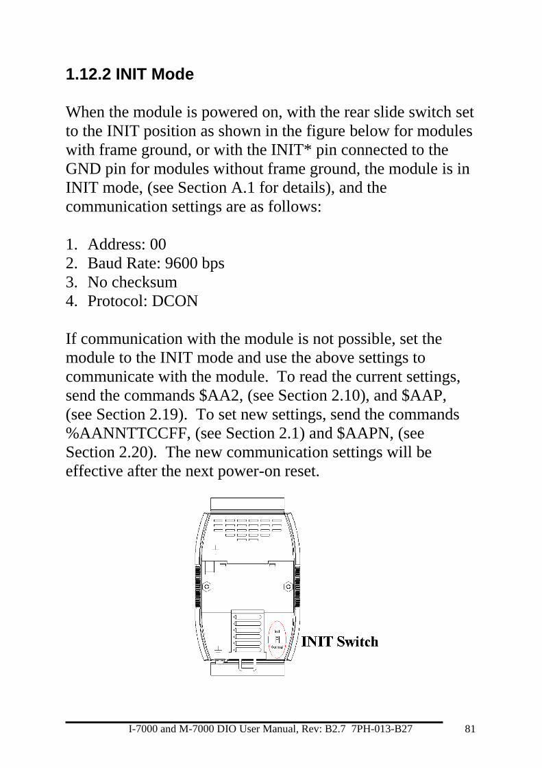
1.12.2 INIT Mode
When the module is powered on, with the rear slide switch set
to the INIT position as shown in the figure below for modules
with frame ground, or with the INIT* pin connected to the
GND pin for modules without frame ground, the module is in
INIT mode, (see Section A.1 for details), and the
communication settings are as follows:
1. Address: 00
2. Baud Rate: 9600 bps
3. No checksum
4. Protocol: DCON
If communication with the module is not possible, set the
module to the INIT mode and use the above settings to
communicate with the module. To read the current settings,
send the commands $AA2, (see Section 2.10), and $AAP,
(see Section 2.19). To set new settings, send the commands
%AANNTTCCFF, (see Section 2.1) and $AAPN, (see
Section 2.20). The new communication settings will be
effective after the next power-on reset.

I-7000 and M-7000 DIO User Manual, Rev: B2.7 7PH-013-B27 82
1.13 Mounting 1.13.1 Din-Rail Mounting
There are three new DIN rail models available. Each is made
of stainless steel, which is stronger than those made of
aluminum. There is a screw at one end and a ring terminal is
included so that it can be easily connected to the earth ground.
The three new DIN rail models are as follows.
Part number Max. number of modules Dimensions
DRS-360 5 360mm x 35mm
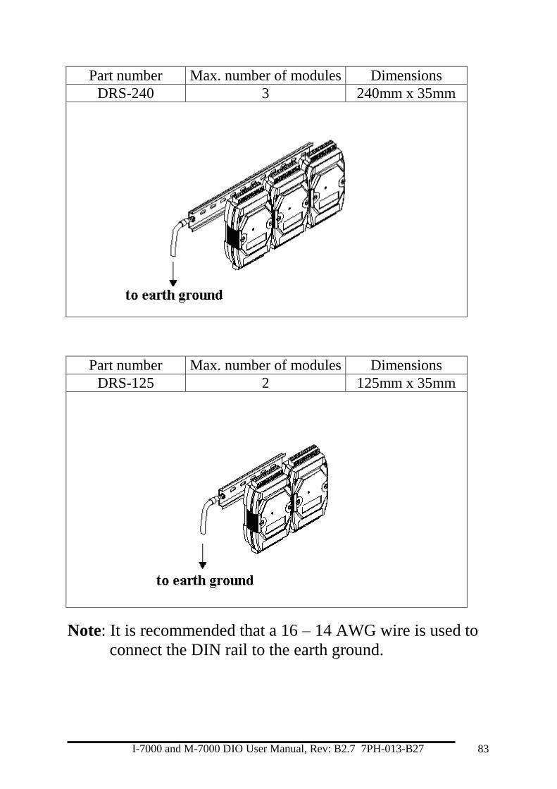
I-7000 and M-7000 DIO User Manual, Rev: B2.7 7PH-013-B27 83
Part number Max. number of modules Dimensions
DRS-240 3 240mm x 35mm
Part number Max. number of modules Dimensions
DRS-125 2 125mm x 35mm
Note: It is recommended that a 16 – 14 AWG wire is used to
connect the DIN rail to the earth ground.
I-7000 and M-7000 DIO User Manual, Rev: B2.7 7PH-013-B27 84
1.13.2 Piggyback Mounting
For I-7041/41D, M-7041/41D, I-7042/42D, I-7043/43D, M-7043/43D,
I-7044/44D, I-7050 series, M-7050 series, I-7052/52D, M-7052/52D,
I-7060/60D, M-7060/60D, I-7063 series, I-7065 series, I-7066/66D, I-7067/67D
and M-7067/67D modules
For I-7045/45D, M-7045/45D, I-7051/51D, M-7051/51D,
I-7053_FG/53D_FG, M-7053/53D, I-7055/55D, M-7055/55D, I-7058/58D,
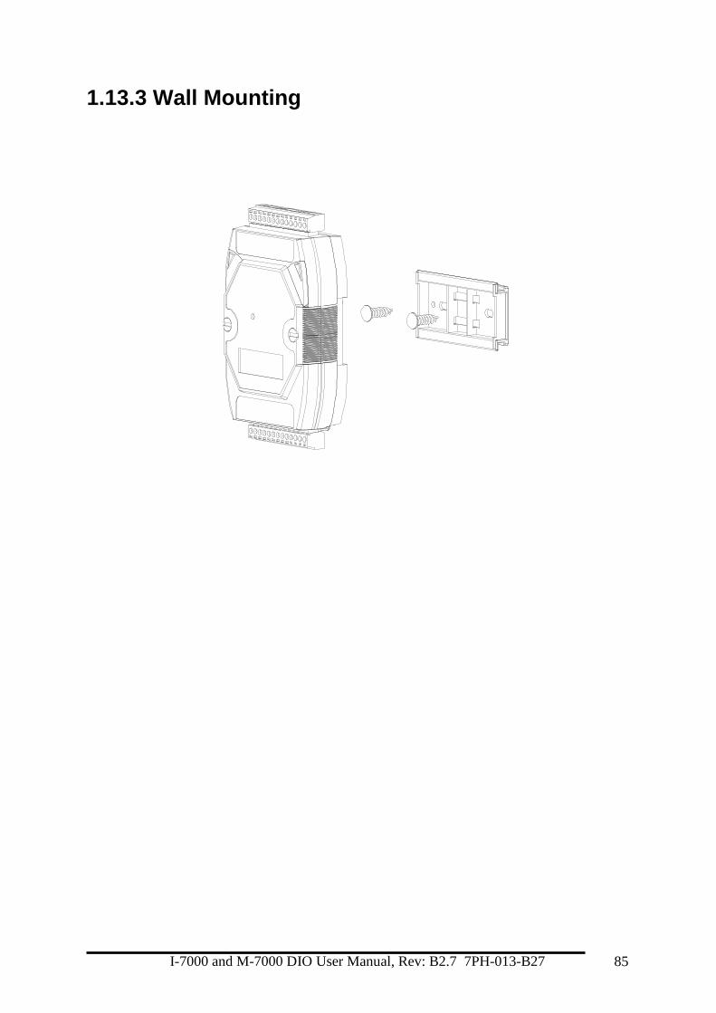
I-7059/59D, and M-7060P modules
I-7000 and M-7000 DIO User Manual, Rev: B2.7 7PH-013-B27 85
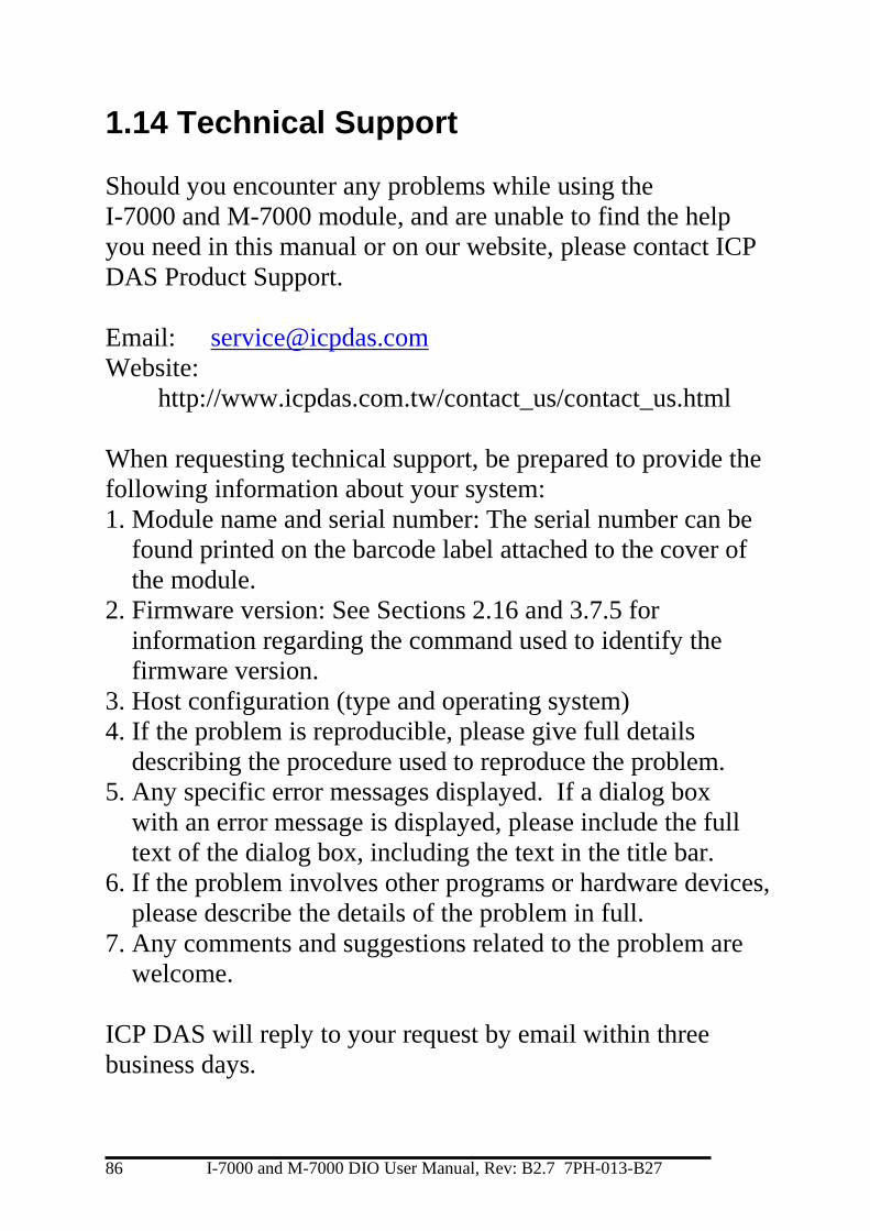
1.13.3 Wall Mounting
I-7000 and M-7000 DIO User Manual, Rev: B2.7 7PH-013-B27 86
1.14 Technical Support
Should you encounter any problems while using the
I-7000 and M-7000 module, and are unable to find the help
you need in this manual or on our website, please contact ICP
DAS Product Support.
Email: [email protected]
Website:
http://www.icpdas.com.tw/contact_us/contact_us.html
When requesting technical support, be prepared to provide the
following information about your system:
1. Module name and serial number: The serial number can be
found printed on the barcode label attached to the cover of
the module.
2. Firmware version: See Sections 2.16 and 3.7.5 for
information regarding the command used to identify the
firmware version.
3. Host configuration (type and operating system)
4. If the problem is reproducible, please give full details
describing the procedure used to reproduce the problem.
5. Any specific error messages displayed. If a dialog box
with an error message is displayed, please include the full
text of the dialog box, including the text in the title bar.
6. If the problem involves other programs or hardware devices,
please describe the details of the problem in full.
7. Any comments and suggestions related to the problem are
welcome.
ICP DAS will reply to your request by email within three
business days.
I-7000 and M-7000 DIO User Manual, Rev: B2.7 7PH-013-B27 87
2. DCON Protocol
All communication with I-7000 modules consists of
commands generated by the host and responses transmitted by
the I-7000 modules. Each module has a unique ID number
that is used for addressing purposes and is stored in non-
volatile memory. The ID is 01 by default and can be changed
using a user command. All commands to the modules contain
the ID address, meaning that only the addressed module will
respond. The only exception to this is commands #**
(Section 2.2) and ~** (Section 2.24), which are sent to all
modules, but in both of these cases, the modules do not reply
to the command.
Command Format:
Leading Character
Module Address
Command [CHKSUM] CR
Response Format:
Leading Character
Module Address
Data [CHKSUM] CR
CHKSUM A 2-character checksum which is present when
the checksum setting is enabled. See Sections
1.10 (Data Format Setting) and 2.1 for details.
CR End of command character, carriage return
(0x0D)
I-7000 and M-7000 DIO User Manual, Rev: B2.7 7PH-013-B27 88
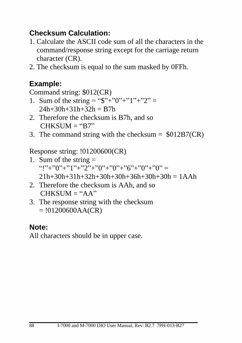
Checksum Calculation: 1. Calculate the ASCII code sum of all the characters in the
command/response string except for the carriage return
character (CR).
2. The checksum is equal to the sum masked by 0FFh.
Example: Command string: $012(CR)
1. Sum of the string = “$”+”0”+”1”+”2” =
24h+30h+31h+32h = B7h
2. Therefore the checksum is B7h, and so
CHKSUM = “B7”
3. The command string with the checksum = $012B7(CR)
Response string: !01200600(CR)
1. Sum of the string =
“!”+”0”+”1”+”2”+”0”+”0”+”6”+”0”+”0” =
21h+30h+31h+32h+30h+30h+36h+30h+30h = 1AAh
2. Therefore the checksum is AAh, and so
CHKSUM = “AA”
3. The response string with the checksum
= !01200600AA(CR)
Note: All characters should be in upper case.

I-7000 and M-7000 DIO User Manual, Rev: B2.7 7PH-013-B27 89
General Command Sets
Command Response Description Section
%AANNTTCCFF !AA Sets the Module Configuration 2.1
#** No Response Synchronized Sampling 2.2
#AA00(Data) > Sets the Digital Output 2.3
#AA0A(Data) > Sets the Digital Output 2.4
#AA0B(Data) > Sets the Digital Output 2.5
#AA1cDD > Sets the Digital Output 2.6
#AAAcDD > Sets the Digital Output 2.7
#AABcDD > Sets the Digital Output. 2.8
#AAN !AA(Data) Reads the Digital Input Counter 2.9
$AA2 !AANNTTCCFF Reads the Module Configuration 2.10
$AA4 !S(Data) Reads the Synchronized Data 2.11
$AA5 !AAS Reads the Reset Status 2.12
$AA6 !(Data) Reads the Digital I/O Status 2.13
$AAC !AA Clears the Latched DI Status 2.14
$AACN !AA Clears the Digital InputCounter 2.15
$AAF !AA(Data) Reads the firmware Version 2.16
$AALS !(Data) Reads the Latched DI Status 2.17
$AAM !AA(Data) Reads the Module Name 2.18
$AAP !AASC Reads the communication protocol 2.19
$AAPN !AA Sets the communication protocol 2.20
@AA >(Data) Reads the Digital I/O Status 2.21
@AA(Data) > Sets the Digital Output Channels 2.22
~AAO(Name) !AA Sets the Module Name 2.23
Host Watchdog Command Sets
Command Response Description Section
~** No Response Host OK 2.24
~AA0 !AASS Reads the Status 2.25
~AA1 !AA Resets the Status 2.26
~AA2 !AAVV Reads the Timeout Settings 2.27
~AA3EVV !AA Sets the Timeout Settings 2.28
~AA4V !AA(Data) Reads the PowerOn/Safe Value 2.29
~AA5V !AA Sets the PowerOn/Safe Value 2.30

I-7000 and M-7000 DIO User Manual, Rev: B2.7 7PH-013-B27 90
2.1 %AANNTTCCFF
Description: Sets the configuration of a module.
Syntax:
%AANNTTCCFF[CHKSUM](CR)
% Delimiter character
AA Address of the module to be configured in
hexadecimal format (00 to FF)
NN New address of the module in hexadecimal format (00
to FF)
TT Type code, should be 40 for DIO module.
CC New Baud Rate code, see Section 1.10 for details.
The INIT* pin must be connected to ground in order
to change Baud Rates. For the module with frame
ground, this is achieved by moving the rear slide
switch to the INIT position. See Section A.1 for
details.
FF Used to set the counter update direction and checksum
(Section 1.10). The INIT* pin must be connected to
ground in order to change the checksum setting. For
the module with frame ground, this is achieved by
moving the rear slide switch to the INIT position. See
Section A.1 for details.

I-7000 and M-7000 DIO User Manual, Rev: B2.7 7PH-013-B27 91
Response: Valid Command: !AA[CHKSUM](CR)
Invalid Command: ?AA[CHKSUM](CR)
! Delimiter for a valid command
? Delimiter for an invalid command. If the Baud Rate
or checksum settings are changed without connecting
the INIT* pin to ground or switching the rear slide
switch to the INIT position, the module will return an
invalid command.
AA Address of the module in hexadecimal format (00 to
FF)
There will be no response if the command syntax is incorrect,
there is a communication error, or there is no module with the
specified address.
Examples: Command: %0102400600 Response: !02
Changes the address of module 01 to 02. The module
returns a valid response.
Command: %0101200A00 Response: ?01
Changes the Baud Rate of module 01 to 115200bps. The
module returns an invalid command, because it is not in
INIT* mode.
Command: %0101200A00 Response: !01
Changes the Baud Rate of module 01 to 115200bps and
the module is in INIT* mode. The module returns a
valid response.
I-7000 and M-7000 DIO User Manual, Rev: B2.7 7PH-013-B27 92
Related Commands: Section 2.10 $AA2
Related Topics: Section 1.10 Configuration Tables, Section A.1 INIT* pin
Operation
Notes: Changes to the address and counter update direction settings
take effect immediately after a valid command is received.
Changes to the Baud Rate and checksum settings take effect
on the next power-on reset.
I-7000 and M-7000 DIO User Manual, Rev: B2.7 7PH-013-B27 93
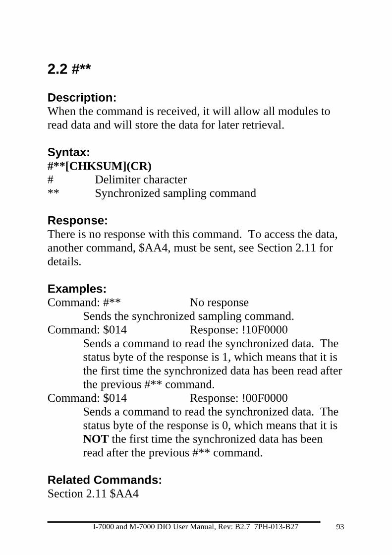
2.2 #**
Description: When the command is received, it will allow all modules to
read data and will store the data for later retrieval.
Syntax: #**[CHKSUM](CR)
# Delimiter character
** Synchronized sampling command
Response: There is no response with this command. To access the data,
another command, $AA4, must be sent, see Section 2.11 for
details.
Examples: Command: #** No response
Sends the synchronized sampling command.
Command: $014 Response: !10F0000
Sends a command to read the synchronized data. The
status byte of the response is 1, which means that it is
the first time the synchronized data has been read after
the previous #** command.
Command: $014 Response: !00F0000
Sends a command to read the synchronized data. The
status byte of the response is 0, which means that it is
NOT the first time the synchronized data has been
read after the previous #** command.
Related Commands: Section 2.11 $AA4
I-7000 and M-7000 DIO User Manual, Rev: B2.7 7PH-013-B27 94
2.3 #AA00(Data)
Description: Sets the digital output value of the lower eight channels.
Syntax: #AA00(Data)[CHKSUM](CR)
# Delimiter character
AA Address of the module to be set (00 to FF)
00 Command to set the digital output value of the
lower eight channels
(Data) A two-digit hexadecimal value, where bit 0
corresponds to DO0, bit 1 corresponds to DO1, etc.
When the bit is 1, it denotes that the digital output
channel is on, and 0 denotes that the digital output
channel is off.
Response: Valid command: >[CHKSUM](CR)
Invalid command: ?[CHKSUM](CR)
Ignored command: 
> Delimiter character for a valid command
? Delimiter character for an invalid command
! Delimiter character for an ignored command. A host
watchdog timeout has occurred, the digital output
channel s are set to safe value, and the digital output
value that was sent is ignored.
There will be no response if the command syntax is incorrect,
there is a communication error, or there is no module with the
specified address.
I-7000 and M-7000 DIO User Manual, Rev: B2.7 7PH-013-B27 95
Examples: Command: #010033 Response: >
Sets DO0, DO1, DO4 and DO5 to on, and DO2, DO3,
DO6, DO7 to off, and the module returns a valid
response.
Related Commands: Section 2.4 #AA0A(data), Section 2.5 #AA0B(data), Section
2.6 #AA1cDD, Section 2.7 #AAAcDD, Section 2.8
#AABcDD, Section 2.13 $AA6, Section 2.21 @AA
Related Topics: Section 1.11 DIO Active States
Notes: 1. This command is only applicable to the modules with
digital output channels.
2. This command is the same as the #AA0A(Data) command.

I-7000 and M-7000 DIO User Manual, Rev: B2.7 7PH-013-B27 96
2.4 #AA0A(Data)
Description: Sets the digital output value of the lower eight channels.
Syntax: #AA0A(Data)[CHKSUM](CR)
# Delimiter character
AA Address of the module to be set (00 to FF)
0A Command to set the digital output value of the
lower eight channels
(Data) A two-digit hexadecimal value, where bit 0
corresponds to DO0, bit 1 corresponds to DO1, etc.
When the bit is 1, it denotes that the digital output
channel is on, and 0 denotes that the digital output
channel is off.
Response: Valid command: >[CHKSUM](CR)
Invalid command: ?[CHKSUM](CR)
Ignored command: 
> Delimiter character for a valid command
? Delimiter character for an invalid command
! Delimiter character for an ignored command. A host
watchdog timeout has occurred, the digital output
channel s are set to safe value, and the digital output
value that was sent is ignored.
There will be no response if the command syntax is incorrect,
there is a communication error, or there is no module with the
specified address.

I-7000 and M-7000 DIO User Manual, Rev: B2.7 7PH-013-B27 97
Examples: Command: #010A33 Response: >
Sets DO0, DO1, DO4 and DO5 to on, and DO2, DO3,
DO6, DO7 to off, and the module returns a valid
response.
Related Commands: Section 2.3 #AA00(data), Section 2.5 #AA0B(data), Section
2.6 #AA1cDD, Section 2.7 #AAAcDD, Section 2.8
#AABcDD, Section 2.13 $AA6, Section 2.21 @AA
Related Topics: Section 1.11 DIO Active States
Notes: 1. This command is only applicable to the modules with
digital output channels.
2. This command is the same as the #AA00(Data) command.

I-7000 and M-7000 DIO User Manual, Rev: B2.7 7PH-013-B27 98
2.5 #AA0B(Data)
Description: Sets the digital output value of the upper eight channels.
Syntax: #AA0B(Data)[CHKSUM](CR)
# Delimiter character
AA Address of the module to be set (00 to FF)
0B Command to set the digital output value of the
upper eight channels
(Data) A two-digit hexadecimal value, where bit 0
corresponds to DO8, bit 1 corresponds to DO9, etc.
When the bit is 1, it denotes that the digital output
channel is on, and 0 denotes that the digital output
channel is off.
Response: Valid command: >[CHKSUM](CR)
Invalid command: ?[CHKSUM](CR)
Ignored command: 
> Delimiter character for a valid command
? Delimiter character for an invalid command
! Delimiter character for an ignored command. A host
watchdog timeout has occurred, the digital output
ports are set to safe value, and the digital output
value that was sent is ignored.
There will be no response if the command syntax is incorrect,
there is a communication error, or there is no module with the
specified address.
I-7000 and M-7000 DIO User Manual, Rev: B2.7 7PH-013-B27 99
Examples: Command: #010B33 Response: >
Sets DO8, DO9, DO12 and DO13 to on, and DO10,
DO11, DO14, DO15 to off, and the module returns a
valid response.
Related Commands: Section 2.3 #AA00(data), Section 2.4 #AA0A(data), Section
2.6 #AA1cDD, Section 2.7 #AAAcDD, Section 2.8
#AABcDD, Section 2.13 $AA6, Section 2.21 @AA
Related Topics: Section 1.11 DIO Active States
Notes: This command is only applicable to the modules with the
number of digital output channels larger than eight.

I-7000 and M-7000 DIO User Manual, Rev: B2.7 7PH-013-B27 100
2.6 #AA1cDD
Description: Sets a single digital output channel of the lower eight
channels.
Syntax: #AA1cDD[CHKSUM](CR)
# Delimiter character
AA Address of the module to be set (00 to FF)
1 Command to set a single digital output channel of the
lower eight channels
c Specifies the digital output channel to be set (0 to 7).
DD 00: set the digital output channel to off.
01: set the digital output channel to on.
Response: Valid command: >[CHKSUM](CR)
Invalid command: ?[CHKSUM](CR)
Ignored command: 
> Delimiter character for a valid command
? Delimiter character for an invalid command
! Delimiter character for an ignored command. A host
watchdog timeout has occurred, the digital output
ports are set to safe value, and the digital output
value that was sent is ignored.
There will be no response if the command syntax is incorrect,
there is a communication error, or there is no module with the
specified address.

I-7000 and M-7000 DIO User Manual, Rev: B2.7 7PH-013-B27 101
Examples: Command: #011201 Response: >
Sets DO2 to on, and the module returns a valid response.
Related Commands: Section 2.3 #AA00(data), Section 2.4 #AA0A(data), Section
2.5 #AA0B(data), Section 2.7 #AAAcDD, Section 2.8
#AABcDD, Section 2.13 $AA6, Section 2.21 @AA
Related Topics: Section 1.11 DIO Active States
Notes: 1. This command is only applicable to the modules with
digital output channels.
2. This command is the same as the #AAAcDD command.

I-7000 and M-7000 DIO User Manual, Rev: B2.7 7PH-013-B27 102
2.7 #AAAcDD
Description: Sets a single digital output channel of the lower eight
channels.
Syntax: #AAAcDD[CHKSUM](CR)
# Delimiter character
AA Address of the module to be set (00 to FF)
A Command to set a single digital output channel of the
lower eight channels
c Specifies the digital output channel to be set (0 to 7).
DD 00: set the digital output channel to off.
01: set the digital output channel to on.
Response: Valid command: >[CHKSUM](CR)
Invalid command: ?[CHKSUM](CR)
Ignored command: 
> Delimiter character for a valid command
? Delimiter character for an invalid command
! Delimiter character for an ignored command. A host
watchdog timeout has occurred, the digital output
ports are set to safe value, and the digital output
value that was sent is ignored.
There will be no response if the command syntax is incorrect,
there is a communication error, or there is no module with the
specified address.

I-7000 and M-7000 DIO User Manual, Rev: B2.7 7PH-013-B27 103
Examples: Command: #01A201 Response: >
Sets DO2 to on, and the module returns a valid response.
Related Commands: Section 2.3 #AA00(data), Section 2.4 #AA0A(data), Section
2.5 #AA0B(data), Section 2.6 #AA1cDD, Section 2.8
#AABcDD, Section 2.13 $AA6, Section 2.21 @AA
Related Topics: Section 1.11 DIO Active States
Notes: 1. This command is only applicable to the modules with
digital output channels.
2. This command is the same as the #AA1cDD command.
I-7000 and M-7000 DIO User Manual, Rev: B2.7 7PH-013-B27 104
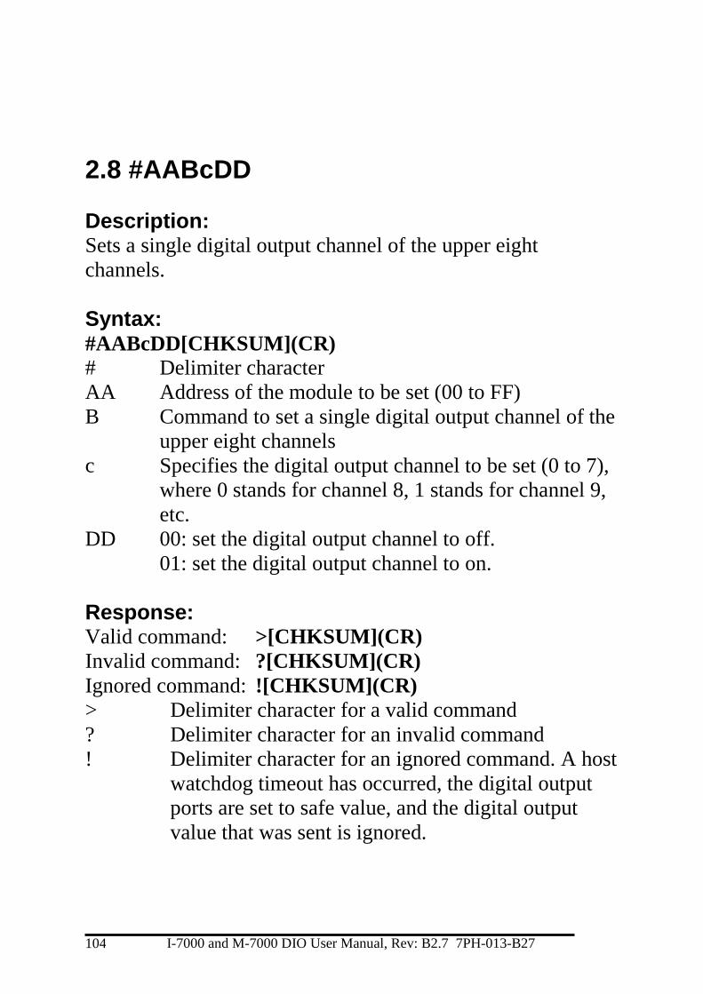
2.8 #AABcDD
Description: Sets a single digital output channel of the upper eight
channels.
Syntax: #AABcDD[CHKSUM](CR)
# Delimiter character
AA Address of the module to be set (00 to FF)
B Command to set a single digital output channel of the
upper eight channels
c Specifies the digital output channel to be set (0 to 7),
where 0 stands for channel 8, 1 stands for channel 9,
etc.
DD 00: set the digital output channel to off.
01: set the digital output channel to on.
Response: Valid command: >[CHKSUM](CR)
Invalid command: ?[CHKSUM](CR)
Ignored command: 
> Delimiter character for a valid command
? Delimiter character for an invalid command
! Delimiter character for an ignored command. A host
watchdog timeout has occurred, the digital output
ports are set to safe value, and the digital output
value that was sent is ignored.
I-7000 and M-7000 DIO User Manual, Rev: B2.7 7PH-013-B27 105
There will be no response if the command syntax is incorrect,
there is a communication error, or there is no module with the
specified address.
Examples: Command: #01B201 Response: >
Sets DO10 to on, and the module returns a valid
response.
Related Commands: Section 2.3 #AA00(data), Section 2.4 #AA0A(data), Section
2.5 #AA0B(data), Section 2.6 #AA1cDD, Section 2.7
#AAAcDD, Section 2.13 $AA6, Section 2.21 @AA
Related Topics: Section 1.11 DIO Active States
Notes: This command is only applicable to the modules with the
number of digital output channels larger than eight.
I-7000 and M-7000 DIO User Manual, Rev: B2.7 7PH-013-B27 106
2.9 #AAN
Description: Reads the digital input counter of channel N.
Syntax: #AAN[CHKSUM](CR)
# Delimiter character
AA Address of the module to be read (00 to FF)
N The channel to be read (0 to F).
Response: Valid Command: !AA(Data)[CHKSUM](CR)
Invalid Command: ?AA[CHKSUM](CR)
! Delimiter character for a valid command
? Delimiter character for an invalid command. An
invalid command is returned if the specified
channel is incorrect.
(Data) Five decimal digits representing the digital input
counter data of the specified channel (00000 to
65535).
AA Address of the responding module (00 to FF)
There will be no response if the command syntax is incorrect,
there is a communication error, or there is no module with the
specified address.

I-7000 and M-7000 DIO User Manual, Rev: B2.7 7PH-013-B27 107
Examples: Command: #032 Response: !0300103
Reads data from channel 2 of module 03 and the returned
counter value is 103.
Command: #029 Response: ?02
Reads data from channel 9 of module 02. An error is
returned because channel 9 is invalid.
Related Commands: Section 2.15 $AACN
Notes: This command is only applicable to the module with digital
inputs.
I-7000 and M-7000 DIO User Manual, Rev: B2.7 7PH-013-B27 108
2.10 $AA2
Description: Reads the module configuration.
Syntax: $AA2[CHKSUM](CR)
$ Delimiter character
AA Address of the module to be read (00 to FF)
2 Command to read the module configuration
Response: Valid Command: !AATTCCFF[CHKSUM](CR)
Invalid Command: ?AA[CHKSUM](CR)
! Delimiter character for a valid command
? Delimiter character for an invalid command
AA Address of the responding module (00 to FF)
TT Type code of the module, should be 40 for DIO
module.
CC Baud Rate code of the module, see Section 1.10 for
details.
FF Checksum and counter update direction settings of
the module, see Section 1.10 for details.
There will be no response if the command syntax is incorrect,
there is a communication error, or there is no module with the
specified address.

I-7000 and M-7000 DIO User Manual, Rev: B2.7 7PH-013-B27 109
Examples: Command: $012 Response: !01400600
Reads the configuration of module 01.
Related Commands: Section 2.1 %AANNTTCCFF
Related Topics: Section 1.10 Configuration Tables
I-7000 and M-7000 DIO User Manual, Rev: B2.7 7PH-013-B27 110
2.11 $AA4
Description: Reads the synchronized data that was retrieved by the last #**
command.
Syntax: $AA4[CHKSUM](CR)
$ Delimiter character
AA Address of the module to be read (00 to FF)
4 Command to read the synchronized data
Response: Valid Command: !S(Data)[CHKSUM](CR)
Invalid Command: ?AA[CHKSUM](CR)
! Delimiter character for a valid command
? Delimiter character for an invalid command
AA Address of the responding module (00 to FF)
S Status of the synchronized data
1: first read
0: not the first read
(Data) Synchronized data. See Section 1.10 for the data
format.
There will be no response if the command syntax is incorrect,
there is a communication error, or there is no module with the
specified address.
I-7000 and M-7000 DIO User Manual, Rev: B2.7 7PH-013-B27 111
Examples: Command: $014 Response: ?01
Reads the synchronized data for module 01. An
invalid command is returned because the #**
command has not been issued in advance.
Command: #** No response
Sends the synchronized sampling command.
Command: $014 Response: !1000F00
Reads the synchronized data for module 01. The
module returns the synchronized data and sets the
status byte to 1 to indicate that this is the first time the
synchronized data has been read.
Command: $014 Response: !0000F00
Reads the synchronized data for module 01. The
module returns the synchronized data and sets the
status byte to 0 to indicate that the synchronized data
has been read.
Related Commands: Section 2.2 #**

I-7000 and M-7000 DIO User Manual, Rev: B2.7 7PH-013-B27 112
2.12 $AA5
Description: Reads the reset status of a module.
Syntax: $AA5[CHKSUM](CR)
$ Delimiter character
AA Address of the module to be read (00 to FF)
5 Command to read the module reset status
Response: Valid Command: !AAS[CHKSUM](CR)
Invalid Command: ?AA[CHKSUM](CR)
! Delimiter character for a valid command
? Delimiter character for an invalid command
AA Address of the responding module (00 to FF)
S Reset status of the module
1: This is the first time the command has been sent
since the module was powered on.
0: This is not the first time the command has been
sent since the module was powered on, which
denotes that there has been no module reset since
the last $AA5 command was sent.
There will be no response if the command syntax is incorrect,
there is a communication error, or there is no module with the
specified address.

I-7000 and M-7000 DIO User Manual, Rev: B2.7 7PH-013-B27 113
Examples: Command: $015 Response: !011
Reads the reset status of module 01. The response
shows that it is the first time the $AA5 command has
been sent since the module was powered-on.
Command: $015 Response: !010
Reads the reset status of module 01. The response
shows that there has been no module reset since the
last $AA5 command was sent.
Related Topics: Section A.4 Reset Status

I-7000 and M-7000 DIO User Manual, Rev: B2.7 7PH-013-B27 114
2.13 $AA6
Description: Reads the status of the digital input/output channels.
Syntax: $AA6[CHKSUM](CR)
$ Delimiter character
AA Address of the module to be read (00 to FF)
6 Command to read the digital input/output channels
Response: Valid command: !(Data)[CHKSUM](CR)
Invalid command: ?AA[CHKSUM](CR)
! Delimiter character for a valid command
? Delimiter character for an invalid command
AA Address of the responding module (00 to FF)
(Data) Status of the digital input/output channels, a four-
digit hexadecimal value followed by 00. See
Section 1.10 for details.
There will be no response if the command syntax is incorrect,
there is a communication error, or there is no module with the
specified address.
I-7000 and M-7000 DIO User Manual, Rev: B2.7 7PH-013-B27 115
Examples: Command: $016 Response: !0F0000
Reads the digital input/output channel status of module
01 (I-7060) and returns 0F0000h, which denotes that
RL1, RL2, RL3 and RL4 are on and IN1, IN2, IN3 and
IN4 are off.
Related Commands: Section 2.21 @AA
Related Topics: Section 1.10 Configuration Tables
I-7000 and M-7000 DIO User Manual, Rev: B2.7 7PH-013-B27 116
2.14 $AAC
Description: Clears the status of the latched digital input and output
channels.
Syntax: $AAC[CHKSUM](CR)
$ Delimiter character
AA Address of the module to be cleared (00 to FF)
C Command to clear the status of the latched digital
input channels
Response: Valid command: !AA[CHKSUM](CR)
Invalid command: ?AA[CHKSUM](CR)
! Delimiter character for a valid command
? Delimiter character for an invalid command
AA Address of the responding module (00 to FF)
There will be no response if the command syntax is incorrect,
there is a communication error, or there is no module with the
specified address.

I-7000 and M-7000 DIO User Manual, Rev: B2.7 7PH-013-B27 117
Examples: Command: $01L0 Response: !FFFF00
Sends the command to read the status of the low latched
digital input channels of module 01 and returns FFFF.
Command: $01C Response: !01
Sends the command to clear the status of the latched
digital input channels of module 01 and returns a valid
response.
Command: $01L0 Response: !000000
Sends the command to read the status of the low latched
digital input channels of module 01 and returns 0000.
Related Commands: Section 2.17 $AALS
Notes: 1. This command is only applicable to the modules with
digital input channels.
2. Both the status of the low and high latched digital input
channels are cleared.
I-7000 and M-7000 DIO User Manual, Rev: B2.7 7PH-013-B27 118
2.15 $AACN
Description: Clears the digital input counter of channel N.
Syntax: $AACN[CHKSUM](CR)
$ Delimiter character
AA Address of the module to be cleared (00 to FF)
C Command to clear the digital input counter
N The channel to be cleared (0 to F).
Response: Valid Command: !AA[CHKSUM](CR)
Invalid Command: ?AA[CHKSUM](CR)
! Delimiter character for a valid command
? Delimiter character for an invalid command. An
invalid command is returned if the specified
channel is incorrect.
AA Address of the responding module (00 to FF)
There will be no response if the command syntax is incorrect,
there is a communication error, or there is no module with the
specified address.

I-7000 and M-7000 DIO User Manual, Rev: B2.7 7PH-013-B27 119
Examples: Command: #032 Response: !0300103
Reads counter data from channel 2 of module 03 and the
returned counter value is 103.
Command: $03C2 Response: !03
Clears the counter value of channel 2 of module 03 and
returns a valid response.
Command: #032 Response: !0300000
Reads counter data from channel 2 of module 03 and the
returned counter value is 3.
Related Commands: Section 2.9 #AAN
Notes: This command is only applicable to the module with digital
inputs.
I-7000 and M-7000 DIO User Manual, Rev: B2.7 7PH-013-B27 120
2.16 $AAF
Description: Reads the firmware version of a module.
Syntax: $AAF[CHKSUM](CR)
$ Delimiter character
AA Address of the module to be read (00 to FF)
F Command to read the firmware version
Response: Valid command: !AA(Data)[CHKSUM](CR)
Invalid command: ?AA[CHKSUM](CR)
! Delimiter character for a valid command
? Delimiter character for an invalid command
AA Address of the responding module (00 to FF)
(Data) Firmware version string of the module
There will be no response if the command syntax is incorrect,
there is a communication error, or there is no module with the
specified address.
Examples: Command: $01F Response: !01A2.0
Reads the firmware version of module 01, and shows
that it is version A2.0.
Command: $02F Response: !02B1.1
Reads the firmware version of module 02, and shows
that it is version B1.1.
I-7000 and M-7000 DIO User Manual, Rev: B2.7 7PH-013-B27 121
2.17 $AALS
Description: Reads the status of the latched digital input and output
channels.
Syntax: $AALS[CHKSUM](CR)
$ Delimiter character
AA Address of the module to be read (00 to FF)
L Command to read the latched status
S 0: read the low latched status
1: read the high latched status
Response: Valid command: !(Data)[CHKSUM](CR)
Invalid command: ?AA[CHKSUM](CR)
! Delimiter character for a valid command
? Delimiter character for an invalid command
AA Address of the responding module (00 to FF)
(Data) Status of the latched digital input channels, a four-
digit hexadecimal value followed by 00. See
Section 1.10 for details.
There will be no response if the command syntax is incorrect,
there is a communication error, or there is no module with the
specified address.

I-7000 and M-7000 DIO User Manual, Rev: B2.7 7PH-013-B27 122
Examples: Command: $01L0 Response: !FFFF00
Sends the command to read the status of the low latched
digital input channels of module 01 and returns FFFF.
Command: $01C Response: !01
Sends the command to clear the status of the latched
digital input channels of module 01 and returns a valid
response.
Command: $01L0 Response: !000000
Sends the command to read the status of the low latched
digital input channels of module 01 and returns 0000.
Related Commands: Section 2.14 $AAC
Related Topics: Section 1.10 Configuration Tables
Notes: This command is only applicable to the modules with digital
input channels.
I-7000 and M-7000 DIO User Manual, Rev: B2.7 7PH-013-B27 123
2.18 $AAM
Description: Reads the name of a module.
Syntax: $AAM[CHKSUM](CR)
$ Delimiter character
AA Address of the module to be read (00 to FF)
M Command to read the module name
Response: Valid command: !AA(Data)[CHKSUM](CR)
Invalid command: ?AA[CHKSUM](CR)
! Delimiter character for a valid command
? Delimiter character for an invalid command
AA Address of the responding module (00 to FF)
(Name) Name string of the module
There will be no response if the command syntax is incorrect,
there is a communication error, or there is no module with the
specified address.
Examples: Command: $01M Response: !017042
Reads the module name of module 01 and returns the
name “7042”.
Related Commands: Section 2.23 ~AAO(Name)
I-7000 and M-7000 DIO User Manual, Rev: B2.7 7PH-013-B27 124
2.19 $AAP
Description: Reads the communication protocol information.
Syntax: $AAP[CHKSUM](CR)
$ Delimiter character
AA Address of the module to be read (00 to FF)
P Command to read the communication protocol
Response: Valid Response: !AASC[CHKSUM](CR)
Invalid Response: ?AA[CHKSUM](CR)
! Delimiter character for a valid response
? Delimiter character for an invalid response
AA Address of the responding module (00 to FF)
S The protocols supported by the module
0: only DCON protocol is supported
1: both the DCON and Modbus RTU protocols are
supported
C The current protocol that is saved in the EEPROM
that will be used at the next power-on reset
0: the protocol set in the EEPROM is DCON
1: the protocol set in the EEPROM is Modbus RTU
There will be no response if the command syntax is incorrect,
there is a communication error, or there is no module with the
specified address.

I-7000 and M-7000 DIO User Manual, Rev: B2.7 7PH-013-B27 125
Examples: Command: $01P Response: !0110
Reads the communication protocol of module 01 and
returns a response of 10 meaning that it supports both
the DCON and Modbus RTU protocols and the
protocol that will be used at the next power-on reset is
DCON.
Related Commands: Section 2.20 $AAPN
Supported modules M-7060/M-7060D/M-7067/M-7067D/M-7050/M-7050D/M-
7051/M-7051D/M-7052/M-7052D/M-7053/M-7053D/M-
7055/M-7055D/M-7041/M-7041D/M-7045/M7045D

I-7000 and M-7000 DIO User Manual, Rev: B2.7 7PH-013-B27 126
2.20 $AAPN
Description: Sets the communication protocol.
Syntax: $AAPN[CHKSUM](CR)
$ Delimiter character
AA Address of the module to be read (00 to FF)
P Command to set the communication protocol
N 0: DCON protocol
1: Modbus RTU protocols
Before using this command, the rear slide switch
must be in the INIT position. The new protocol is
saved in the EEPROM and will be effective after
the next power-on reset.
Response: Valid Response: !AASC[CHKSUM](CR)
Invalid Response: ?AA[CHKSUM](CR)
! Delimiter character for a valid response
? Delimiter character for an invalid response
AA Address of the responding module (00 to FF)
There will be no response if the command syntax is incorrect,
there is a communication error, or there is no module with the
specified address.
I-7000 and M-7000 DIO User Manual, Rev: B2.7 7PH-013-B27 127
Examples: Command: $01P1 Response: ?01
Sets the communication protocol of module 01 to
Modbus RTU and returns an invalid response because
the module is not in INIT mode.
Command: $01P1 Response: !01
Sets the communication protocol of module 01 to
Modbus RTU and returns a valid response.
Related Commands: Section 2.19 $AAP
Supported modules M-7060/M-7060D/M-7067/M-7067D/M-7050/M-7050D/M-
7051/M-7051D/M-7052/M-7052D/M-7053/M-7053D/M-
7055/M-7055D/M-7041/M-7041D/M-7045/M7045D
I-7000 and M-7000 DIO User Manual, Rev: B2.7 7PH-013-B27 128
2.21 @AA
Description: Reads the status of the digital input/output ports.
Syntax: @AA[CHKSUM](CR)
@ Delimiter character
AA Address of the module to be read (00 to FF)
Response: Valid command: >(Data)[CHKSUM](CR)
Invalid command: ?AA[CHKSUM](CR)
> Delimiter character for a valid command
? Delimiter character for an invalid command or
invalid type code
AA Address of the responding module (00 to FF)
(Data) Status of the digital input/output ports, a four-digit
hexadecimal value. See Section 1.10 for details.
There will be no response if the command syntax is incorrect,
there is a communication error, or there is no module with the
specified address.

I-7000 and M-7000 DIO User Manual, Rev: B2.7 7PH-013-B27 129
Examples: Command: @01 Response: >0F00
Reads the digital input/output port status of module 01
(I-7060) and returns 0F00h, which denotes that RL1,
RL2, RL3 and RL4 are on and IN1, IN2, IN3 and IN4
are off.
Related Commands: Section 2.13 $AA6
Related Topics: Section 1.10 Configuration Tables

I-7000 and M-7000 DIO User Manual, Rev: B2.7 7PH-013-B27 130
2.22 @AA(Data)
Description: Sets the digital output channels.
Syntax: @AA(Data)[CHKSUM](CR)
@ Delimiter character
AA Address of the module to be set (00 to FF)
(Data) Data to be written to the digital output channels.
For the I-7060 and I-7063 series, it is a one-digit
hexadecimal value. For the I-7044, I-7050, I-7055,
I-7065, I-7066 and I-7067 series, it is a two-digit
hexadecimal value. For the I-7042, I-7043 and I-
7045 series, it is a four-digit hexadecimal value. Bit
0 of the value corresponds to DO0 and bit 1 of the
value corresponds to DO1, etc. When the bit is 1, it
denotes that the digital output channel is on, and 0
denotes that the digital output channel is off.
Response: Valid command: >[CHKSUM](CR)
Invalid command: ?[CHKSUM](CR)
Ignored command: 
> Delimiter character for a valid command
? Delimiter character for an invalid command
! Delimiter character for an ignored command. A host
watchdog timeout has occurred, the digital output
ports are set to safe value, and the digital output
value that was sent is ignored.

I-7000 and M-7000 DIO User Manual, Rev: B2.7 7PH-013-B27 131
There will be no response if the command syntax is incorrect,
there is a communication error, or there is no module with the
specified address.
Examples: Command: @017 Response: >
For the I-7060 module, sets DO0 to on, DO1 to on, DO2
to on, and DO3 to off, and the module returns a valid
response.
Command: @0207 Response: >
For the I-7050 module, sets DO0 to on, DO1 to on, DO2
to on, and other channels to off, and the module returns a
valid response.
Command: @030001 Response: >
For the I-7045 module, sets DO0 to on and other
channels to off, and the module returns a valid response.
Related Commands: Section 2.21 @AA
Related Topics: Section 1.11 DIO Active States
Notes: This command is only applicable to the modules with digital
output channels.
I-7000 and M-7000 DIO User Manual, Rev: B2.7 7PH-013-B27 132
2.23 ~AAO(Name)
Description: Sets the name of a module.
Syntax: ~AAO(Name)[CHKSUM](CR)
~ Delimiter character
AA Address of the module to be set (00 to FF)
O Command to set the module name
(Name) New name of the module (max. 6 characters).
Response: Valid command: !AA[CHKSUM](CR)
Invalid command: ?AA[CHKSUM](CR)
! Delimiter character for a valid command
? Delimiter character for an invalid command
AA Address of the responding module (00 to FF)
There will be no response if the command syntax is incorrect,
there is a communication error, or there is no module with the
specified address.
I-7000 and M-7000 DIO User Manual, Rev: B2.7 7PH-013-B27 133
Examples: Command: ~01O7050N Response: !01
Sets the name of module 01 to be “7050N” and returns a
valid response.
Command: $01M Response: !017050N
Reads the name of module 01 and returns the name
“7050N”.
Related Commands: Section 2.18 $AAM
I-7000 and M-7000 DIO User Manual, Rev: B2.7 7PH-013-B27 134
2.24 ~**
Description: Informs all modules that the host is OK.
Syntax: ~**[CHKSUM](CR)
~ Delimiter character
** Host OK command
Response: No response.
Examples: Command: ~** No response
Sends a “Host OK” command to all modules.
Related Commands: Section 2.25 ~AA0, Section 2.26 ~AA1, Section 2.27 ~AA2,
Section 2.28 ~AA3EVV, Section 2.29 ~AA4V, Section 2.30
~AA5V
Related Topics: Section A.2 Dual Watchdog Operation
I-7000 and M-7000 DIO User Manual, Rev: B2.7 7PH-013-B27 135
2.25 ~AA0
Description: Reads the host watchdog status of a module.
Syntax: ~AA0[CHKSUM](CR)
~ Delimiter character
AA Address of the module to be read (00 to FF)
0 Command to read the module status
Response: Valid command: !AASS[CHKSUM](CR)
Invalid command: ?AA[CHKSUM](CR)
! Delimiter character for a valid command
? Delimiter character for an invalid command
AA Address of the responding module (00 to FF)
SS Two hexadecimal digits that represent the host
watchdog status, where:
Bit 7: 0 indicates that the host watchdog is disabled,
and 1 indicates that the host watchdog is enabled,
Bit 2: 1 indicates that a host watchdog timeout has
occurred, and 0 indicates that no host watchdog
timeout has occurred.
The host watchdog status is stored in EEPROM and
can only be reset by using the ~AA1 command.

I-7000 and M-7000 DIO User Manual, Rev: B2.7 7PH-013-B27 136
There will be no response if the command syntax is incorrect,
there is a communication error, or there is no module with the
specified address.
Examples: Command: ~010 Response: !0100
Reads the host watchdog status of module 01 and returns
00, meaning that the host watchdog is disabled and no
host watchdog timeout has occurred.
Command: ~020 Response: !0204
Reads the host watchdog status of module 02 and returns
04, meaning that a host watchdog timeout has occurred.
Related Commands: Section 2.24 ~**, Section 2.26 ~AA1, Section 2.27 ~AA2,
Section 2.28 ~AA3EVV, Section 2.29 ~AA4V, Section 2.30
~AA5V
Related Topics: Section A.2 Dual Watchdog Operation

I-7000 and M-7000 DIO User Manual, Rev: B2.7 7PH-013-B27 137
2.26 ~AA1
Description: Resets the host watchdog timeout status of a module.
Syntax: ~AA1[CHKSUM](CR)
~ Delimiter character
AA Address of the module to be reset (00 to FF)
1 Command to reset the host watchdog timeout status
Response: Valid command: !AA[CHKSUM](CR)
Invalid command: ?AA[CHKSUM](CR)
! Delimiter character for a valid command
? Delimiter character for an invalid command
AA Address of the responding module (00 to FF)
There will be no response if the command syntax is incorrect,
there is a communication error, or there is no module with the
specified address.
I-7000 and M-7000 DIO User Manual, Rev: B2.7 7PH-013-B27 138
Examples: Command: ~010 Response: !0104
Reads the host watchdog status of module 01 and shows
that a host watchdog timeout has occurred.
Command: ~011 Response: !01
Resets the host watchdog timeout status of module 01
and returns a valid response.
Command: ~010 Response: !0100
Reads the host watchdog status of module 01 and shows
that no host watchdog timeout has occurred.
Related Commands: Section 2.24 ~**, Section 2.25 ~AA0, Section 2.27 ~AA2,
Section 2.28 ~AA3EVV, Section 2.29 ~AA4V, Section 2.30
~AA5V
Related Topics: Section A.2 Dual Watchdog Operation

I-7000 and M-7000 DIO User Manual, Rev: B2.7 7PH-013-B27 139
2.27 ~AA2
Description: Reads the host watchdog timeout value of a module.
Syntax: ~AA2[CHKSUM](CR)
~ Delimiter character
AA Address of the module to be read (00 to FF)
2 Command to read the host watchdog timeout value
Response: Valid command : !AAEVV[CHKSUM](CR)
Invalid command: ?AA[CHKSUM](CR)
! Delimiter character for a valid command
? Delimiter character for an invalid command
AA Address of the responding module (00 to FF)
E 1: the host watchdog is enabled
0: the host watchdog is disabled
VV Two hexadecimal digits to represent the timeout
value in tenths of a second, for example, 01 denotes
0.1 seconds and FF denotes 25.5 seconds.
There will be no response if the command syntax is incorrect,
there is a communication error, or there is no module with the
specified address.
I-7000 and M-7000 DIO User Manual, Rev: B2.7 7PH-013-B27 140
Examples: Command: ~012 Response: !011FF
Reads the host watchdog timeout value of module 01
and returns FF, which denotes that the host watchdog
is enabled and the host watchdog timeout value is 25.5
seconds.
Related Commands: Section 2.24 ~**, Section 2.25 ~AA0, Section 2.26 ~AA1,
Section 2.28 ~AA3EVV, Section 2.29 ~AA4V, Section 2.30
~AA5V
Related Topics: Section A.2 Dual Watchdog Operation
I-7000 and M-7000 DIO User Manual, Rev: B2.7 7PH-013-B27 141
2.28 ~AA3EVV
Description: Enables/disables the host watchdog and sets the host
watchdog timeout value of a module.
Syntax: ~AA3EVV[CHKSUM](CR)
~ Delimiter character
AA Address of the module to be set (00 to FF)
3 Command to set the host watchdog
E 1: enable the host watchdog
0: disable the host watchdog
VV Two hexadecimal digits to represent the timeout
value in tenths of a second, for example, 01 denotes
0.1 seconds and FF denotes 25.5 seconds.
Response: Valid command: !AA[CHKSUM](CR)
Invalid command: ?AA[CHKSUM](CR)
! Delimiter character for a valid command
? Delimiter character for an invalid command
AA Address of the responding module (00 to FF)
There will be no response if the command syntax is incorrect,
there is a communication error, or there is no module with the
specified address.

I-7000 and M-7000 DIO User Manual, Rev: B2.7 7PH-013-B27 142
Examples: Command: ~013164 Response: !01
Enables the host watchdog of module 01 and sets the
host watchdog timeout value to 10.0 seconds. The
module returns a valid response.
Command: ~012 Response: !01164
Reads the host watchdog timeout value of module 01.
The module returns 164, which denotes that the host
watchdog is enabled and the host watchdog timeout
value is 10.0 seconds.
Related Commands: Section 2.24 ~**, Section 2.25 ~AA0, Section 2.26 ~AA1,
Section 2.27 ~AA2, Section 2.29 ~AA4V, Section 2.30
~AA5V
Related Topics: Section A.2 Dual Watchdog Operation
Notes: When a host watchdog timeout occurs, the host watchdog is
disabled. The ~AA3EVV command should be sent again to
reenable the host watchdog.
I-7000 and M-7000 DIO User Manual, Rev: B2.7 7PH-013-B27 143
2.29 ~AA4V
Description: Reads the power-on DO value or the safe DO value of a
module.
Syntax: ~AA4V[CHKSUM](CR)
~ Delimiter character
AA Address of the module to be read (00 to FF)
4 Command to read the power-on DO value or the
safe DO value
V P: Reads the power-on DO value
S: Reads the safe DO value
Response: Valid command : !AA(Data)[CHKSUM](CR)
Invalid command: ?AA[CHKSUM](CR)
! Delimiter character for a valid command
? Delimiter character for an invalid command
AA Address of the responding module (00 to FF)
(Data) Power-on DO value or safe DO value.
For the I-7042/42D/43/43D/45/45D modules, they
are four hexadecimal digits. For other modules,
they are two hexadecimal digits followed by 00.
There will be no response if the command syntax is incorrect,
there is a communication error, or there is no module with the
specified address.

I-7000 and M-7000 DIO User Manual, Rev: B2.7 7PH-013-B27 144
Examples: Command: ~014S Response: !010000
Reads the safe DO value of module 01 and returns
0000.
Command: ~014P Response: !01FF00
Reads the power-on DO value of module 01 and
returns FF00.
Related Commands: Section 2.30 ~AA5V
Related Topics: Section 1.11 DIO Active States, Section A.2 Dual Watchdog
Operation
Notes: This command is only applicable to the modules with digital
output channels.

I-7000 and M-7000 DIO User Manual, Rev: B2.7 7PH-013-B27 145
2.30 ~AA5V
Description: Sets the current DO value as the power-on DO value or the
safe DO value.
Syntax: ~AA5V[CHKSUM](CR)
~ Delimiter character
AA Address of the module to be set (00 to FF)
5 Command to set the power-on value or the safe DO
value
V P: Sets the power-on DO value
S: Sets the safe DO value
Response: Valid command: !AA[CHKSUM](CR)
Invalid command: ?AA[CHKSUM](CR)
! Delimiter character for a valid command
? Delimiter character for an invalid command
AA Address of the responding module (00 to FF)
There will be no response if the command syntax is incorrect,
there is a communication error, or there is no module with the
specified address.

I-7000 and M-7000 DIO User Manual, Rev: B2.7 7PH-013-B27 146
Examples: Command: @01AA Response: >
Sets the DO value of module 01 to AA and the module
returns a valid response.
Command: ~015P Response: !01
Sets the power-on DO value and the module returns a
valid response.
Command: @0155 Response: >
Sets the DO value of module 01 to 55 and the module
returns a valid response.
Command: ~015S Response: !01
Sets the safe DO value and the module returns a valid
response.
Command: ~014P Response: !01AA00
Reads the power-on DO value of module 01. The
module returns AA00, which denotes that the power-
on DO value is AA.
Command: ~014S Response: !015500
Reads the safe DO value of module 01. The module
returns 5500, which denotes that the safe DO value is
55.
Related Commands: Section 2.29 ~AA4V
Related Topics: Section A.2 Dual Watchdog Operation
Notes: This command is only applicable to the modules with the
digital output channels.

I-7000 and M-7000 DIO User Manual, Rev: B2.7 7PH-013-B27 147
2.31 ~AAD
Description: Reads the miscellaneous settings of a module.
Syntax: ~AAD[CHKSUM](CR)
~ Delimiter character
AA Address of the module to be read (00 to FF)
D Command to read the miscellaneous settings
Response: Valid Command: !AAT[CHKSUM](CR)
Invalid Command: ?AA[CHKSUM](CR)
! Delimiter character for a valid command
? Delimiter character for an invalid command
AA Address of the responding module (00 to FF)
VV Two hexadecimal digits that represent the
miscellaneous settings as follows:
7 6 5 4 3 2 1 0
Reserved OA IA
Key Description
OA DO active state 0: output value 1 for relay active
output value 0 for relay inactive 1: output value 0 for relay active
output value 1 for relay inactive IA DI active state
0: input value 1 for non-signal or the low voltage; input value 0 for high voltage
1: input value 0 for non-signal or the low voltage; input value 1 for high voltage
I-7000 and M-7000 DIO User Manual, Rev: B2.7 7PH-013-B27 148
There will be no response if the command syntax is incorrect,
there is a communication error, or there is no module with the
specified address.
Examples: Command: ~01D Response: !0101
Reads the miscellaneous settings of module 01 and
returns 01.
Related Commands: Section 2.32 ~AADVV
Notes: This command is only applicable to the M-7000 DIO modules.
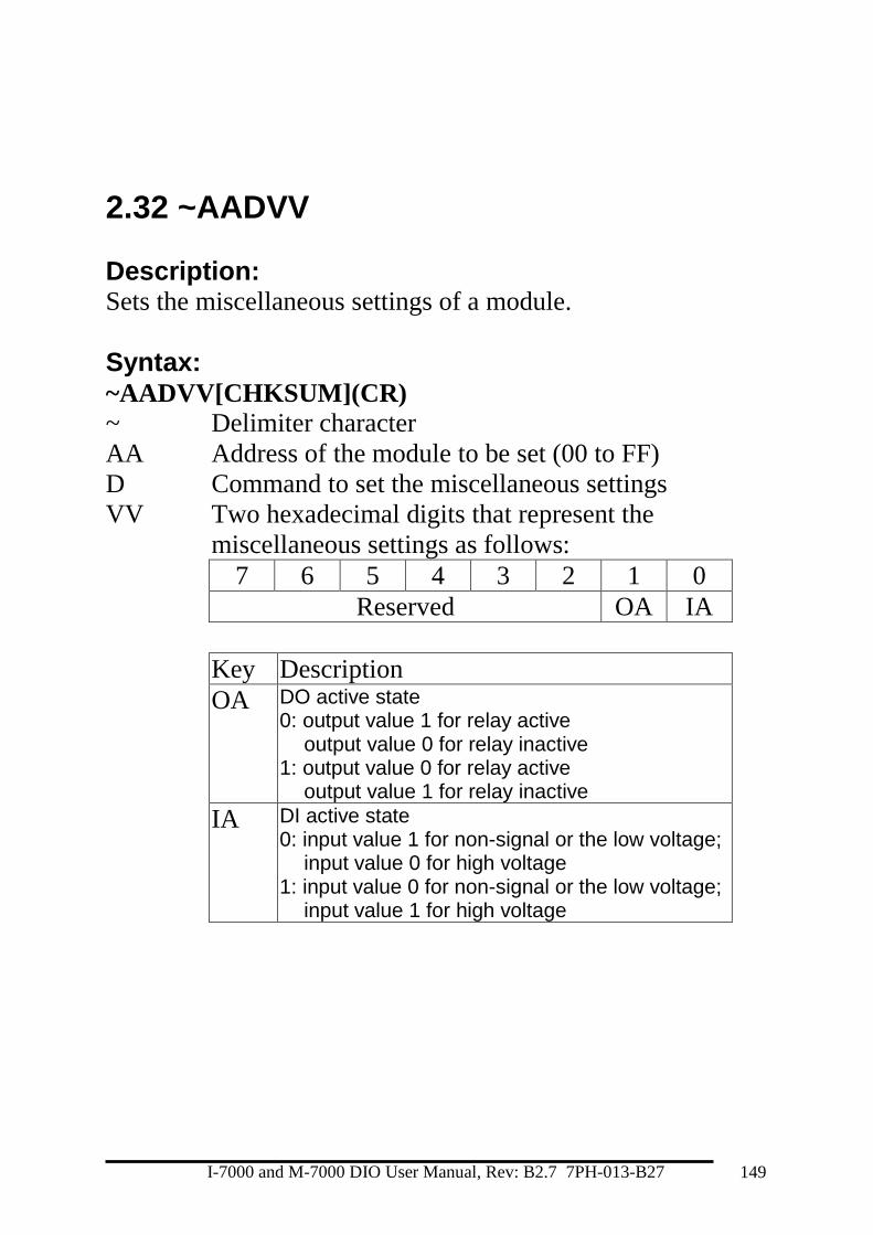
I-7000 and M-7000 DIO User Manual, Rev: B2.7 7PH-013-B27 149
2.32 ~AADVV
Description: Sets the miscellaneous settings of a module.
Syntax: ~AADVV[CHKSUM](CR)
~ Delimiter character
AA Address of the module to be set (00 to FF)
D Command to set the miscellaneous settings
VV Two hexadecimal digits that represent the
miscellaneous settings as follows:
7 6 5 4 3 2 1 0
Reserved OA IA
Key Description
OA DO active state 0: output value 1 for relay active
output value 0 for relay inactive 1: output value 0 for relay active
output value 1 for relay inactive IA DI active state
0: input value 1 for non-signal or the low voltage; input value 0 for high voltage
1: input value 0 for non-signal or the low voltage; input value 1 for high voltage

I-7000 and M-7000 DIO User Manual, Rev: B2.7 7PH-013-B27 150
Response: Valid Command: !AA[CHKSUM](CR)
Invalid Command: ?AA[CHKSUM](CR)
! Delimiter character for a valid command
? Delimiter character for an invalid command
AA Address of the responding module (00 to FF)
There will be no response if the command syntax is incorrect,
there is a communication error, or there is no module with the
specified address.
Examples: Command: ~01D01 Response: !01
Sets the miscellaneous settings of module 01 to 01,
and returns a valid response.
Related Commands: Section 2.31 ~AAD
Notes: This command is only applicable to the M-7000 DIO modules.
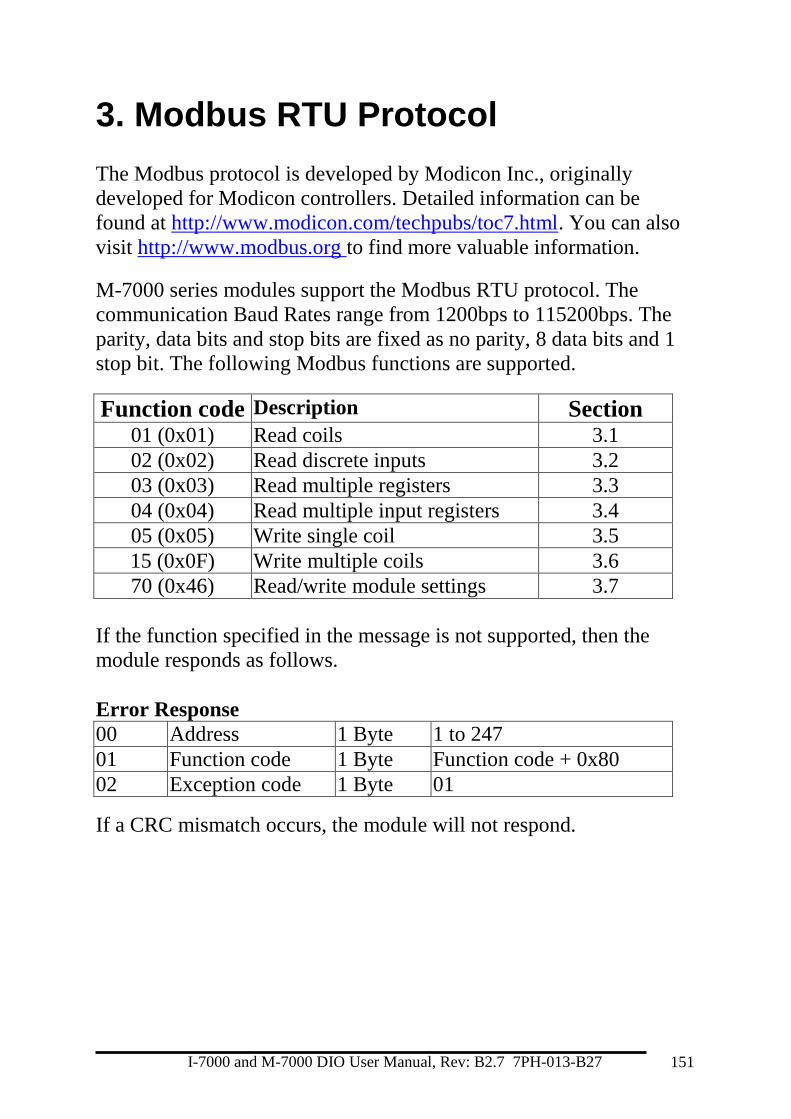
I-7000 and M-7000 DIO User Manual, Rev: B2.7 7PH-013-B27 151
3. Modbus RTU Protocol
The Modbus protocol is developed by Modicon Inc., originally
developed for Modicon controllers. Detailed information can be
found at http://www.modicon.com/techpubs/toc7.html. You can also
visit http://www.modbus.org to find more valuable information.
M-7000 series modules support the Modbus RTU protocol. The
communication Baud Rates range from 1200bps to 115200bps. The
parity, data bits and stop bits are fixed as no parity, 8 data bits and 1
stop bit. The following Modbus functions are supported.
Function code Description Section 01 (0x01) Read coils 3.1
02 (0x02) Read discrete inputs 3.2
03 (0x03) Read multiple registers 3.3
04 (0x04) Read multiple input registers 3.4
05 (0x05) Write single coil 3.5
15 (0x0F) Write multiple coils 3.6
70 (0x46) Read/write module settings 3.7
If the function specified in the message is not supported, then the
module responds as follows.
Error Response
00 Address 1 Byte 1 to 247
01 Function code 1 Byte Function code + 0x80
02 Exception code 1 Byte 01
If a CRC mismatch occurs, the module will not respond.
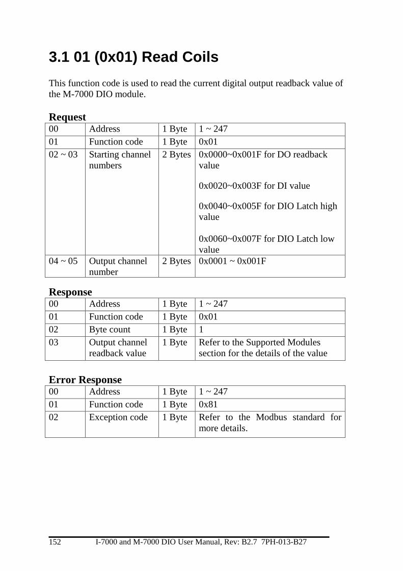
I-7000 and M-7000 DIO User Manual, Rev: B2.7 7PH-013-B27 152
3.1 01 (0x01) Read Coils This function code is used to read the current digital output readback value of
the M-7000 DIO module.
Request 00 Address 1 Byte 1 ~ 247
01 Function code 1 Byte 0x01
02 ~ 03 Starting channel
numbers
2 Bytes 0x0000~0x001F for DO readback
value
0x0020~0x003F for DI value
0x0040~0x005F for DIO Latch high
value
0x0060~0x007F for DIO Latch low
value
04 ~ 05 Output channel
number
2 Bytes 0x0001 ~ 0x001F
Response 00 Address 1 Byte 1 ~ 247
01 Function code 1 Byte 0x01
02 Byte count 1 Byte 1
03 Output channel
readback value
1 Byte Refer to the Supported Modules
section for the details of the value
Error Response 00 Address 1 Byte 1 ~ 247
01 Function code 1 Byte 0x81
02 Exception code 1 Byte Refer to the Modbus standard for
more details.

I-7000 and M-7000 DIO User Manual, Rev: B2.7 7PH-013-B27 153
Supported Modules
M-7060/M-7060D:
Valid starting
channel
0x0000~0x 0003 for DO readback value
0x0020~0x0023 for DI value
0x0040~0x0043 for DI Latch high value
0x0044~0x0047 for DO Latch high value
0x0060~0x0063 for DI Latch low value
0x0064~0x0067 for DO Latch low value
M-7061/M-7061D:
Valid starting
channel
0x0000~0x 000B for DO readback value
0x0040~0x004B for DO Latch high value
0x0060~0x006B for DO Latch low value
M-7064/M-7064D:
Valid starting
channel
0x0000~0x 0007 for DO readback value
0x0040~0x0047 for DO Latch high value
0x0060~0x0067 for DO Latch low value
M-7067/M-7067D:
Valid starting
channel
0x0000~0x 0006 for DO readback value
0x0040~0x0046 for DO Latch high value
0x0060~0x0066 for DO Latch low value
M-7055/M-7055D/M-7055U/M-7055UD:
Valid starting
channel
0x0000~0x 0007 for DO readback value
0x0020~0x0027 for DI value
0x0040~0x0047 for DI Latch high value
0x0048~0x004F for DO Latch high value
0x0060~0x0067 for DI Latch low value
0x0068~0x006F for DO Latch low value
M-7052/M-7052D:
Valid starting
channel
0x0020~0x0027 for DI value
0x0040~0x0047 for DI Latch high value
0x0060~0x0067 for DI Latch low value
M-7053/M-7053D:
Valid starting
channel
0x0020~0x002F for DI value
0x0040~0x004F for DI Latch high value
0x0060~0x006F for DI Latch low value

I-7000 and M-7000 DIO User Manual, Rev: B2.7 7PH-013-B27 154
M-7058/M-7058D:
Valid starting
channel
0x0020~0x0027 for DI value
0x0040~0x0047 for DI Latch high value
0x0060~0x0067 for DI Latch low value
M-7041/M-7041D:
Valid starting
channel
0x0020~0x002D for DI value
0x0040~0x004D for DI Latch high value
0x0060~0x006D for DI Latch low value
M-7043/M-7043D:
Valid starting
channel
0x0000~0x 000F for DO readback value
0x0040~0x004F for DO Latch high value
0x0060~0x006F for DO Latch low value
M-7045/M-7045D:
Valid starting
channel
0x0000~0x 000F for DO readback value
0x0040~0x004F for DO Latch high value
0x0060~0x006F for DO Latch low value
M-7046/M-7046D:
Valid starting
channel
0x0020~0x002E for DI value
0x0040~0x004E for DI Latch high value
0x0060~0x006E for DI Latch low value
M-7051/M-7051D:
Valid starting
channel
0x0020~0x002F for DI value
0x0040~0x004F for DI Latch high value
0x0060~0x006F for DI Latch low value
M-7050/M-7050D:
Valid starting
channel
0x0000~0x 0007 for DO readback value
0x0020~0x0026 for DI value
0x0040~0x0046 for DI Latch high value
0x0048~0x004F for DO Latch high value
0x0060~0x0066 for DI Latch low value
0x0068~0x006F for DO Latch low value
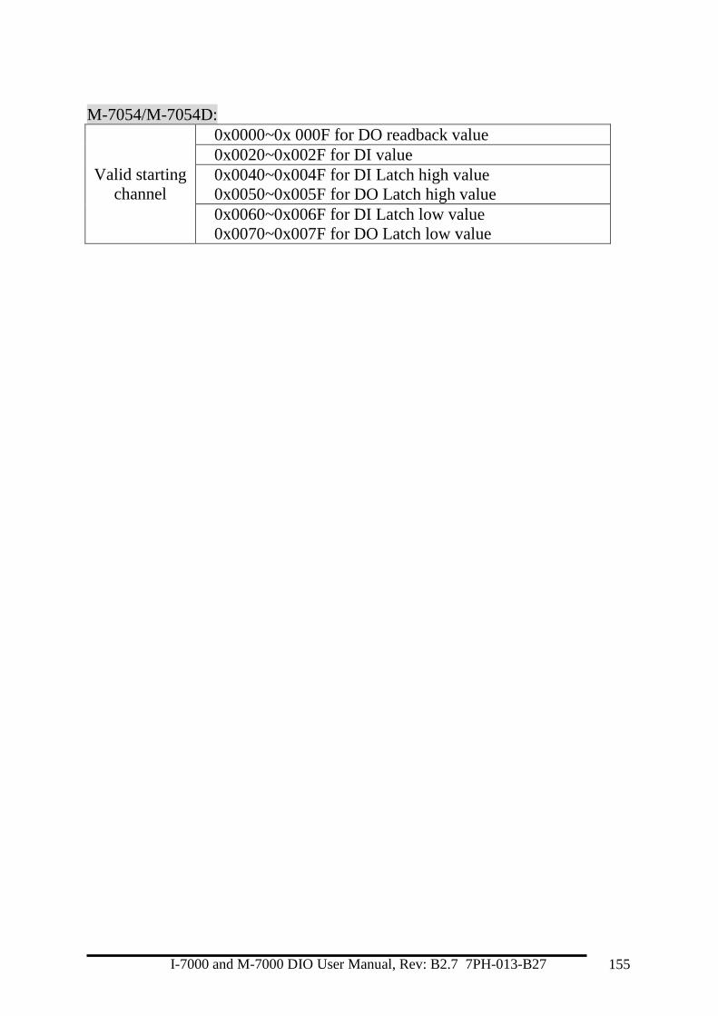
I-7000 and M-7000 DIO User Manual, Rev: B2.7 7PH-013-B27 155
M-7054/M-7054D:
Valid starting
channel
0x0000~0x 000F for DO readback value
0x0020~0x002F for DI value
0x0040~0x004F for DI Latch high value
0x0050~0x005F for DO Latch high value
0x0060~0x006F for DI Latch low value
0x0070~0x007F for DO Latch low value
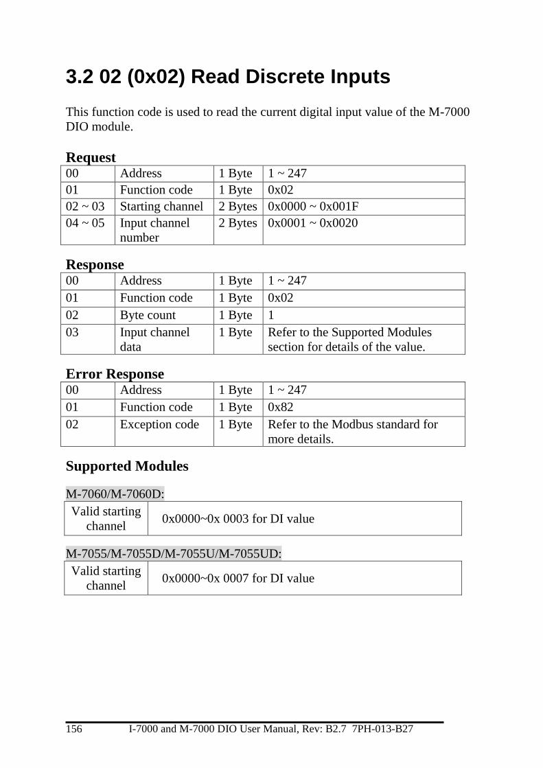
I-7000 and M-7000 DIO User Manual, Rev: B2.7 7PH-013-B27 156
3.2 02 (0x02) Read Discrete Inputs This function code is used to read the current digital input value of the M-7000
DIO module.
Request 00 Address 1 Byte 1 ~ 247
01 Function code 1 Byte 0x02
02 ~ 03 Starting channel 2 Bytes 0x0000 ~ 0x001F
04 ~ 05 Input channel
number
2 Bytes 0x0001 ~ 0x0020
Response 00 Address 1 Byte 1 ~ 247
01 Function code 1 Byte 0x02
02 Byte count 1 Byte 1
03 Input channel
data
1 Byte Refer to the Supported Modules
section for details of the value.
Error Response 00 Address 1 Byte 1 ~ 247
01 Function code 1 Byte 0x82
02 Exception code 1 Byte Refer to the Modbus standard for
more details.
Supported Modules
M-7060/M-7060D:
Valid starting
channel 0x0000~0x 0003 for DI value
M-7055/M-7055D/M-7055U/M-7055UD:
Valid starting
channel 0x0000~0x 0007 for DI value

I-7000 and M-7000 DIO User Manual, Rev: B2.7 7PH-013-B27 157
M-7052/M-7052D:
Valid starting
channel 0x0000~0x0007 for DI value
M-7053/M-7053D:
Valid starting
channel 0x0000~0x000F for DI value
M-7058/M-7058D:
Valid starting
channel 0x0000~0x0007 for DI value
M-7041/M-7041D:
Valid starting
channel 0x0000~0x000D for DI value
M-7046/M-7046D:
Valid starting
channel 0x0000~0x000E for DI value
M-7051/M-7051D:
Valid starting
channel 0x0000~0x000F for DI value
M-7050/M-7050D:
Valid starting
channel 0x0000~0x 0006 for DI value
M-7054/M-7054D:
Valid starting
channel 0x0000~0x 000F for DI value

I-7000 and M-7000 DIO User Manual, Rev: B2.7 7PH-013-B27 158
3.3 03 (0x03) Read Multiple Registers This function code is used to read the current digital input counter value of the
M-7000 DIO module.
Request 00 Address 1 Byte 1 ~ 247
01 Function code 1 Byte 0x03
02 ~ 03 Starting channel
numbers
2 Bytes 0x0000 ~ 0x001F
04 ~ 05 Input channel
number
2 Bytes 0x0001 ~ 0x0020
Response 00 Address 1 Byte 1 ~ 247
01 Function code 1 Byte 0x03
02 Byte count 1 Byte 1
03~ Input channel
counter value
*N x 2
Bytes
Each channel can record a maximum
counter value up to 65535 (0xFFFF).
*N = Number of input channels
Error Response 00 Address 1 Byte 1 ~ 247
01 Function code 1 Byte 0x83
02 Exception code 1 Byte Refer to the Modbus standard for
more details.
Supported Modules
M-7060/M-7060D:
Valid starting
channel 0x0000~0x 0003 for DI counter value
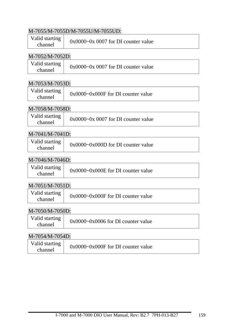
I-7000 and M-7000 DIO User Manual, Rev: B2.7 7PH-013-B27 159
M-7055/M-7055D/M-7055U/M-7055UD:
Valid starting
channel 0x0000~0x 0007 for DI counter value
M-7052/M-7052D:
Valid starting
channel 0x0000~0x 0007 for DI counter value
M-7053/M-7053D:
Valid starting
channel 0x0000~0x000F for DI counter value
M-7058/M-7058D:
Valid starting
channel 0x0000~0x 0007 for DI counter value
M-7041/M-7041D:
Valid starting
channel 0x0000~0x000D for DI counter value
M-7046/M-7046D:
Valid starting
channel 0x0000~0x000E for DI counter value
M-7051/M-7051D:
Valid starting
channel 0x0000~0x000F for DI counter value
M-7050/M-7050D:
Valid starting
channel 0x0000~0x0006 for DI counter value
M-7054/M-7054D:
Valid starting
channel 0x0000~0x000F for DI counter value

I-7000 and M-7000 DIO User Manual, Rev: B2.7 7PH-013-B27 160
3.4 04 (0x04) Read Multiple Input Registers This function code is used to read the current digital input counter value of the
M-7000 DIO module.
Request 00 Address 1 Byte 1 ~ 247
01 Function code 1 Byte 0x04
02 ~ 03 Starting channel
numbers
2 Bytes 0x0000 ~ 0x001F
04 ~ 05 Input channel
number
2 Bytes 0x0001 ~ 0x0020
Response 00 Address 1 Byte 1 ~ 247
01 Function code 1 Byte 0x04
02 Byte count 1 Byte 1
03~ Input channel
counter value
*N x 2
Bytes
Each channel can record the
maximum counter value up to 65535
(0xFFFF).
*N = Number of input channels
Error Response 00 Address 1 Byte 1 ~ 247
01 Function code 1 Byte 0x84
02 Exception code 1 Byte Refer to the Modbus standard for
more details.
Supported Modules
M-7060/M-7060D:
Valid starting
channel 0x0000~0x 0003 for DI counter value

I-7000 and M-7000 DIO User Manual, Rev: B2.7 7PH-013-B27 161
M-7055/M-7055D/M-7055U/M-7055UD:
Valid starting
channel 0x0000~0x 0007 for DI counter value
M-7052/M-7052D:
Valid starting
channel 0x0000~0x 0007 for DI counter value
M-7053/M-7053D:
Valid starting
channel 0x0000~0x000F for DI counter value
M-7058/M-7058D:
Valid starting
channel 0x0000~0x 0007 for DI counter value
M-7041/M-7041D:
Valid starting
channel 0x0000~0x000D for DI counter value
M-7046/M-7046D:
Valid starting
channel 0x0000~0x000E for DI counter value
M-7051/M-7051D:
Valid starting
channel 0x0000~0x000F for DI counter value
M-7050/M-7050D:
Valid starting
channel 0x0000~0x0006 for DI counter value
M-7054/M-7054D:
Valid starting
channel 0x0000~0x000F for DI counter value

I-7000 and M-7000 DIO User Manual, Rev: B2.7 7PH-013-B27 162
3.5 05 (0x05) Write Single Coils This function code is used to write the digital output value of the M-7000 DIO
module.
Request 00 Address 1 Byte 1 ~ 247
01 Function code 1 Byte 0x05
02 ~ 03 Output channel
numbers
2 Bytes 0x0000 ~ 0x001F
0x0100 to clear the latch value
0x0200~0x021F to clear the DI
counter value
04 ~ 05 Output value 2 Bytes A value of 0xFF00 sets the output to
ON. A value of 0x0000 sets it to
OFF. All other values are illegal and
will not affect the coil.
Response 00 Address 1 Byte 1 ~ 247
01 Function code 1 Byte 0x05
02 ~ 03 Output channel
numbers
2 Bytes The value is the same as byte 02 and
03 of the Request
04 ~ 05 Output value 2 Bytes The value is the same as byte 04 and
05 of the Request
Error Response 00 Address 1 Byte 1 ~ 247
01 Function code 1 Byte 0x85
02 Exception code 1 Byte Refer to the Modbus standard for
more details.
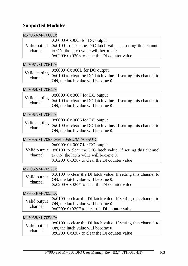
I-7000 and M-7000 DIO User Manual, Rev: B2.7 7PH-013-B27 163
Supported Modules
M-7060/M-7060D:
Valid output
channel
0x0000~0x0003 for DO output
0x0100 to clear the DIO latch value. If setting this channel
to ON, the latch value will become 0.
0x0200~0x0203 to clear the DI counter value
M-7061/M-7061D:
Valid starting
channel
0x0000~0x 000B for DO output
0x0100 to clear the DO latch value. If setting this channel to
ON, the latch value will become 0.
M-7064/M-7064D:
Valid starting
channel
0x0000~0x 0007 for DO output
0x0100 to clear the DO latch value. If setting this channel to
ON, the latch value will become 0.
M-7067/M-7067D:
Valid starting
channel
0x0000~0x 0006 for DO output
0x0100 to clear the DO latch value. If setting this channel to
ON, the latch value will become 0.
M-7055/M-7055D/M-7055U/M-7055UD:
Valid output
channel
0x0000~0x 0007 for DO output
0x0100 to clear the DIO latch value. If setting this channel
to ON, the latch value will become 0.
0x0200~0x0207 to clear the DI counter value
M-7052/M-7052D:
Valid output
channel
0x0100 to clear the DI latch value. If setting this channel to
ON, the latch value will become 0.
0x0200~0x0207 to clear the DI counter value
M-7053/M-7053D:
Valid output
channel
0x0100 to clear the DI latch value. If setting this channel to
ON, the latch value will become 0.
0x0200~0x020F to clear the DI counter value
M-7058/M-7058D:
Valid output
channel
0x0100 to clear the DI latch value. If setting this channel to
ON, the latch value will become 0.
0x0200~0x0207 to clear the DI counter value

I-7000 and M-7000 DIO User Manual, Rev: B2.7 7PH-013-B27 164
M-7041/M-7041D:
Valid output
channel
0x0100 to clear the DI latch value. If setting this channel to
ON, the latch value will become 0.
0x0200~0x020D to clear the DI counter value
M-7043/M-7043D:
Valid starting
channel
0x0000~0x 000F for DO output
0x0100 to clear the DO latch value. If setting this channel to
ON, the latch value will become 0.
M-7045/M-7045D:
Valid starting
channel
0x0000~0x 000F for DO output
0x0100 to clear the DO latch value. If setting this channel to
ON, the latch value will become 0.
M-7046/M-7046D:
Valid output
channel
0x0100 to clear the DI latch value. If setting this channel to
ON, the latch value will become 0.
0x0200~0x020E to clear the DI counter value
M-7051/M-7051D:
Valid output
channel
0x0100 to clear the DI latch value. If setting this channel to
ON, the latch value will become 0.
0x0200~0x020F to clear the DI counter value
M-7050/M-7050D:
Valid output
channel
0x0000~0x 0007 for DO output
0x0100 to clear the DIO latch value. If setting this channel
to ON, the latch value will become 0.
0x0200~0x0206 to clear the DI counter value
M-7054/M-7054D:
Valid output
channel
0x0000~0x 000F for DO output
0x0100 to clear the DIO latch value. If setting this channel
to ON, the latch value will become 0.
0x0200~0x020F to clear the DI counter value

I-7000 and M-7000 DIO User Manual, Rev: B2.7 7PH-013-B27 165
3.6 15 (0x0F) Write Multiple Coils This function code is used to write the digital output value of the M-7000 DIO
module.
Request 00 Address 1 Byte 1 ~ 247
01 Function code 1 Byte 0x0F
02 ~ 03 Starting channel 2 Bytes 0x0000 ~ 0x001F for DO output
0x0200~0x021F to clear the DI
count value
04 ~ 05 Number of
output channels
2 Bytes 0x0001 ~ 0x0020
06 Byte count (N) 1 Byte Number of bytes of the following
output values, 0x01 ~ 0x02
07 Data of output
channels
N
Bytes
A bit corresponds to a channel.
When the bit is 1 it denotes that the
value of the channel that was set is
ON. If the bit is 0 it denotes that the
value of the channel that was set is
OFF.
Response 00 Address 1 Byte 1 ~ 247
01 Function code 1 Byte 0x0F
02 ~ 03 Starting channel 2 Bytes The value is the same as byte 02 and
03 of the Request
04 ~ 05 Number of
output channels
2 Bytes The value is the same as byte 04 and
05 of the Request
Error Response 00 Address 1 Byte 1 ~ 247
01 Function code 1 Byte 0x8F
02 Exception code 1 Byte Refer to the Modbus standard for
more details.
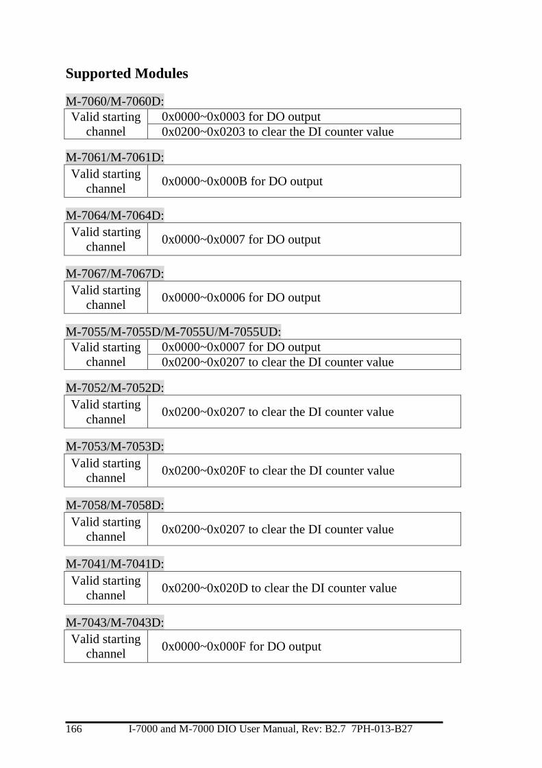
I-7000 and M-7000 DIO User Manual, Rev: B2.7 7PH-013-B27 166
Supported Modules
M-7060/M-7060D:
Valid starting
channel
0x0000~0x0003 for DO output
0x0200~0x0203 to clear the DI counter value
M-7061/M-7061D:
Valid starting
channel 0x0000~0x000B for DO output
M-7064/M-7064D:
Valid starting
channel 0x0000~0x0007 for DO output
M-7067/M-7067D:
Valid starting
channel 0x0000~0x0006 for DO output
M-7055/M-7055D/M-7055U/M-7055UD:
Valid starting
channel
0x0000~0x0007 for DO output
0x0200~0x0207 to clear the DI counter value
M-7052/M-7052D:
Valid starting
channel 0x0200~0x0207 to clear the DI counter value
M-7053/M-7053D:
Valid starting
channel 0x0200~0x020F to clear the DI counter value
M-7058/M-7058D:
Valid starting
channel 0x0200~0x0207 to clear the DI counter value
M-7041/M-7041D:
Valid starting
channel 0x0200~0x020D to clear the DI counter value
M-7043/M-7043D:
Valid starting
channel 0x0000~0x000F for DO output
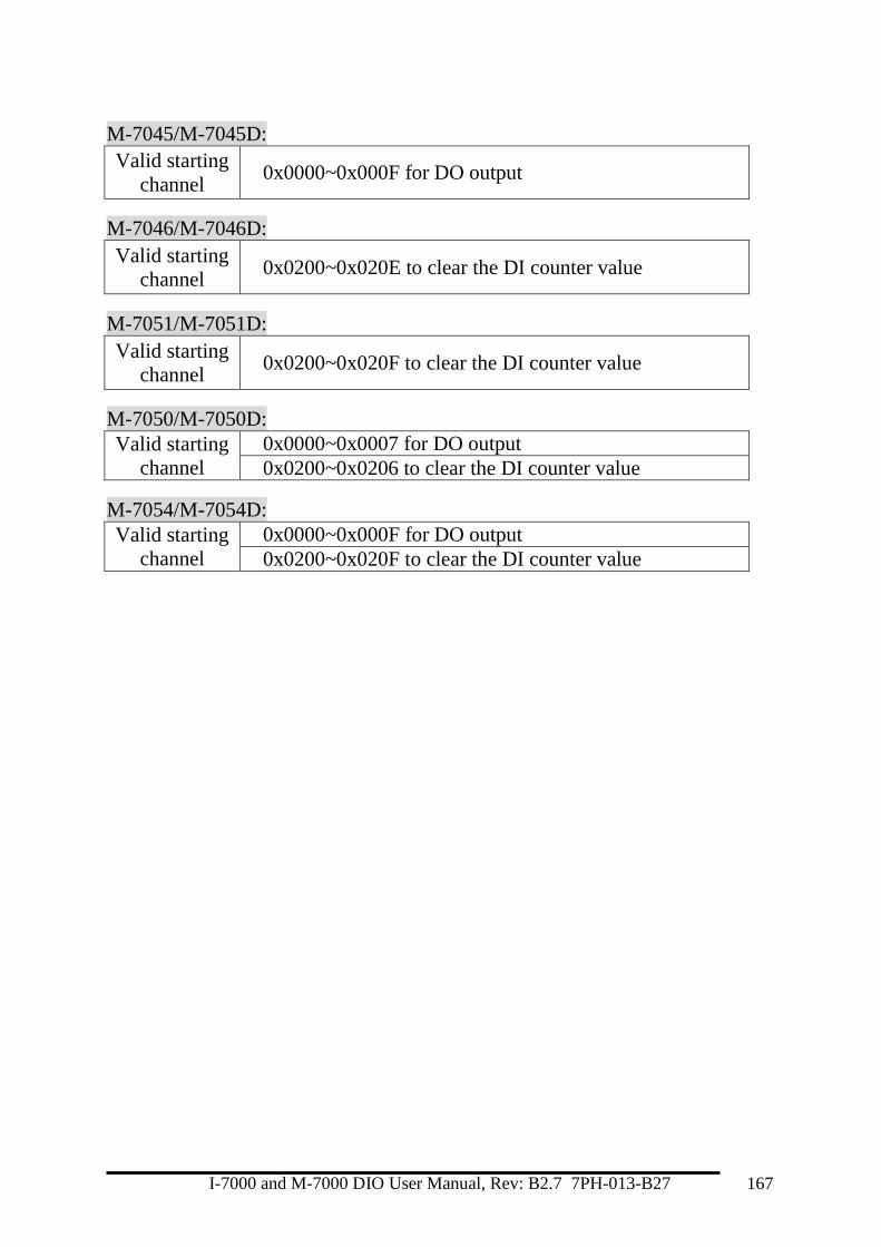
I-7000 and M-7000 DIO User Manual, Rev: B2.7 7PH-013-B27 167
M-7045/M-7045D:
Valid starting
channel 0x0000~0x000F for DO output
M-7046/M-7046D:
Valid starting
channel 0x0200~0x020E to clear the DI counter value
M-7051/M-7051D:
Valid starting
channel 0x0200~0x020F to clear the DI counter value
M-7050/M-7050D:
Valid starting
channel
0x0000~0x0007 for DO output
0x0200~0x0206 to clear the DI counter value
M-7054/M-7054D:
Valid starting
channel
0x0000~0x000F for DO output
0x0200~0x020F to clear the DI counter value

I-7000 and M-7000 DIO User Manual, Rev: B2.7 7PH-013-B27 168
3.7 70 (0x46) Read/Write Module Settings
This function code is used to read the settings of the module or
change the settings of the module. The following sub-function codes
are supported.
Sub-function Code Description Section
00 (0x00) Read the module name 3.7.1
04 (0x04) Set the module address 3.7.2
05 (0x05) Read the communication settings 3.7.3
06 (0x06) Set the communication settings 3.7.4
32 (0x20) Read the firmware version 3.7.5
33 (0x21) Set the DI count edge 3.7.6
34 (0x22) Read the DI count edge setting value 3.7.7
39 (0x27) Set the DO power-on value 3.7.8
40 (0x28) Read the DO power-on value 3.7.9
41 (0x29) Set the DI/O active states 3.7.10
42 (0x2A) Read the DI/O active states 3.7.11
If the module does not support the sub-function code specified in the
message, then it responds as follows:
Error Response
00 Address 1 Byte 1 ~ 247
01 Function code 1 Byte 0xC6
02 Exception code 1 Byte Refer to the Modbus standard for
more details.
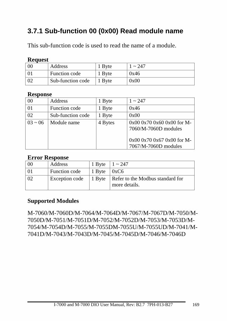
I-7000 and M-7000 DIO User Manual, Rev: B2.7 7PH-013-B27 169
3.7.1 Sub-function 00 (0x00) Read module name This sub-function code is used to read the name of a module.
Request 00 Address 1 Byte 1 ~ 247
01 Function code 1 Byte 0x46
02 Sub-function code 1 Byte 0x00
Response 00 Address 1 Byte 1 ~ 247
01 Function code 1 Byte 0x46
02 Sub-function code 1 Byte 0x00
03 ~ 06 Module name 4 Bytes 0x00 0x70 0x60 0x00 for M-
7060/M-7060D modules
0x00 0x70 0x67 0x00 for M-
7067/M-7060D modules
Error Response 00 Address 1 Byte 1 ~ 247
01 Function code 1 Byte 0xC6
02 Exception code 1 Byte Refer to the Modbus standard for
more details.
Supported Modules
M-7060/M-7060D/M-7064/M-7064D/M-7067/M-7067D/M-7050/M-
7050D/M-7051/M-7051D/M-7052/M-7052D/M-7053/M-7053D/M-
7054/M-7054D/M-7055/M-7055DM-7055U/M-7055UD/M-7041/M-
7041D/M-7043/M-7043D/M-7045/M-7045D/M-7046/M-7046D
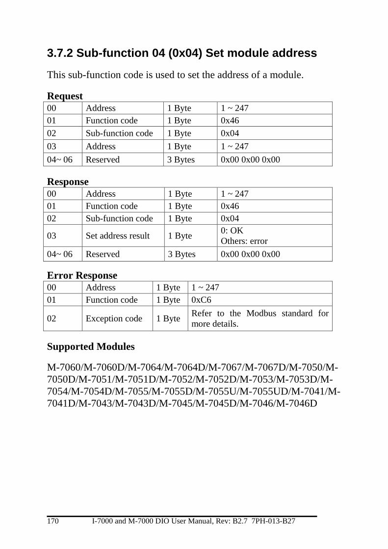
I-7000 and M-7000 DIO User Manual, Rev: B2.7 7PH-013-B27 170
3.7.2 Sub-function 04 (0x04) Set module address
This sub-function code is used to set the address of a module.
Request
00 Address 1 Byte 1 ~ 247
01 Function code 1 Byte 0x46
02 Sub-function code 1 Byte 0x04
03 Address 1 Byte 1 ~ 247
04~ 06 Reserved 3 Bytes 0x00 0x00 0x00
Response 00 Address 1 Byte 1 ~ 247
01 Function code 1 Byte 0x46
02 Sub-function code 1 Byte 0x04
03 Set address result 1 Byte 0: OK
Others: error
04~ 06 Reserved 3 Bytes 0x00 0x00 0x00
Error Response 00 Address 1 Byte 1 ~ 247
01 Function code 1 Byte 0xC6
02 Exception code 1 Byte Refer to the Modbus standard for
more details.
Supported Modules
M-7060/M-7060D/M-7064/M-7064D/M-7067/M-7067D/M-7050/M-
7050D/M-7051/M-7051D/M-7052/M-7052D/M-7053/M-7053D/M-
7054/M-7054D/M-7055/M-7055D/M-7055U/M-7055UD/M-7041/M-
7041D/M-7043/M-7043D/M-7045/M-7045D/M-7046/M-7046D
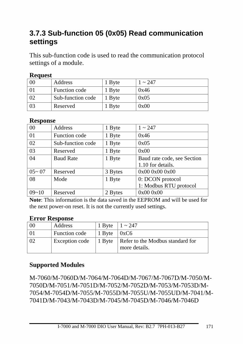
I-7000 and M-7000 DIO User Manual, Rev: B2.7 7PH-013-B27 171
3.7.3 Sub-function 05 (0x05) Read communication settings
This sub-function code is used to read the communication protocol
settings of a module.
Request 00 Address 1 Byte 1 ~ 247
01 Function code 1 Byte 0x46
02 Sub-function code 1 Byte 0x05
03 Reserved 1 Byte 0x00
Response 00 Address 1 Byte 1 ~ 247
01 Function code 1 Byte 0x46
02 Sub-function code 1 Byte 0x05
03 Reserved 1 Byte 0x00
04 Baud Rate 1 Byte Baud rate code, see Section
1.10 for details.
05~ 07 Reserved 3 Bytes 0x00 0x00 0x00
08 Mode 1 Byte 0: DCON protocol
1: Modbus RTU protocol
09~10 Reserved 2 Bytes 0x00 0x00
Note: This information is the data saved in the EEPROM and will be used for
the next power-on reset. It is not the currently used settings.
Error Response 00 Address 1 Byte 1 ~ 247
01 Function code 1 Byte 0xC6
02 Exception code 1 Byte Refer to the Modbus standard for
more details.
Supported Modules
M-7060/M-7060D/M-7064/M-7064D/M-7067/M-7067D/M-7050/M-
7050D/M-7051/M-7051D/M-7052/M-7052D/M-7053/M-7053D/M-
7054/M-7054D/M-7055/M-7055D/M-7055U/M-7055UD/M-7041/M-
7041D/M-7043/M-7043D/M-7045/M-7045D/M-7046/M-7046D

I-7000 and M-7000 DIO User Manual, Rev: B2.7 7PH-013-B27 172
3.7.4 Sub-function 06 (0x06) Set communication settings
This sub-function code is used to set the communication protocol of a
module.
Request 00 Address 1 Byte 1 ~ 247
01 Function code 1 Byte 0x46
02 Sub-function code 1 Byte 0x06
03 Reserved 1 Byte 0x00
04 Baud Rate 1 Byte Baud rate code, see Section
1.10 for details.
05~ 07 Reserved 3 Bytes 0x00 0x00 0x00
08 Mode 1 Byte 0: DCON protocol
1: Modbus RTU protocol
09~10 Reserved 2 Bytes 0x00 0x00
Response 00 Address 1 Byte 1 ~ 247
01 Function code 1 Byte 0x46
02 Sub-function code 1 Byte 0x06
03 Reserved 1 Byte 0x00
04 Baud Rate 1 Byte 0: OK,
others: error
05~ 07 Reserved 3 Bytes 0x00 0x00 0x00
08 Mode 1 Byte 0: OK,
others: error
09~10 Reserved 2 Bytes 0x00 0x00
Note: The new baud rate and protocol will be effective after the next power-on
reset.

I-7000 and M-7000 DIO User Manual, Rev: B2.7 7PH-013-B27 173
Error Response 00 Address 1 Byte 1 ~ 247
01 Function code 1 Byte 0xC6
02 Exception code 1 Byte Refer to the Modbus standard for
more details.
Supported Module
M-7060/M-7060D/M-7064/M-7064D/M-7067/M-7067D/M-7050/M-
7050D/M-7051/M-7051D/M-7052/M-7052D/M-7053/M-7053D/M-
7054/M-7054D/M-7055/M-7055D/M-7055U/M-7055UD/M-7041/M-
7041D/M-7043/M-7043D/M-7045/M-7045D/M-7046/M-7046D
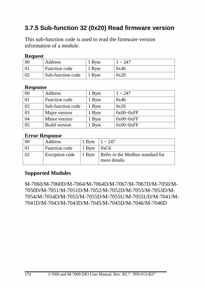
I-7000 and M-7000 DIO User Manual, Rev: B2.7 7PH-013-B27 174
3.7.5 Sub-function 32 (0x20) Read firmware version
This sub-function code is used to read the firmware version
information of a module.
Request
00 Address 1 Byte 1 ~ 247
01 Function code 1 Byte 0x46
02 Sub-function code 1 Byte 0x20
Response 00 Address 1 Byte 1 ~ 247
01 Function code 1 Byte 0x46
02 Sub-function code 1 Byte 0x20
03 Major version 1 Byte 0x00~0xFF
04 Minor version 1 Byte 0x00~0xFF
05 Build version 1 Byte 0x00~0xFF
Error Response 00 Address 1 Byte 1 ~ 247
01 Function code 1 Byte 0xC6
02 Exception code 1 Byte Refer to the Modbus standard for
more details.
Supported Modules
M-7060/M-7060D/M-7064/M-7064D/M-7067/M-7067D/M-7050/M-
7050D/M-7051/M-7051D/M-7052/M-7052D/M-7053/M-7053D/M-
7054/M-7054D/M-7055/M-7055D/M-7055U/M-7055UD/M-7041/M-
7041D/M-7043/M-7043D/M-7045/M-7045D/M-7046/M-7046D
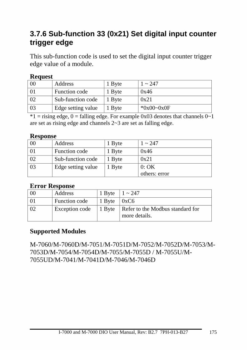
I-7000 and M-7000 DIO User Manual, Rev: B2.7 7PH-013-B27 175
3.7.6 Sub-function 33 (0x21) Set digital input counter trigger edge
This sub-function code is used to set the digital input counter trigger
edge value of a module.
Request 00 Address 1 Byte 1 ~ 247
01 Function code 1 Byte 0x46
02 Sub-function code 1 Byte 0x21
03 Edge setting value 1 Byte *0x00~0x0F
*1 = rising edge, 0 = falling edge. For example 0x03 denotes that channels 0~1
are set as rising edge and channels 2~3 are set as falling edge.
Response 00 Address 1 Byte 1 ~ 247
01 Function code 1 Byte 0x46
02 Sub-function code 1 Byte 0x21
03 Edge setting value 1 Byte 0: OK
others: error
Error Response 00 Address 1 Byte 1 ~ 247
01 Function code 1 Byte 0xC6
02 Exception code 1 Byte Refer to the Modbus standard for
more details.
Supported Modules
M-7060/M-7060D/M-7051/M-7051D/M-7052/M-7052D/M-7053/M-
7053D/M-7054/M-7054D/M-7055/M-7055D / M-7055U/M-
7055UD/M-7041/M-7041D/M-7046/M-7046D

I-7000 and M-7000 DIO User Manual, Rev: B2.7 7PH-013-B27 176
3.7.7 Sub-function 34 (0x22) Read digital input counter trigger edge value
This sub-function code is used to read the digital input counter trigger
edge value of a module.
Request 00 Address 1 Byte 1 ~ 247
01 Function code 1 Byte 0x46
02 Sub-function code 1 Byte 0x22
Response 00 Address 1 Byte 1 ~ 247
01 Function code 1 Byte 0x46
02 Sub-function code 1 Byte 0x22
03 Edge setting value 1 Byte *0x00~0x0F
*1 = rising edge, 0 = falling edge. For example 0x03 denotes that channels 0~1
are set as rising edge and channels 2~3 are set as falling edge.
Error Response 00 Address 1 Byte 1 ~ 247
01 Function code 1 Byte 0xC6
02 Exception code 1 Byte Refer to the Modbus standard for
more details.
Supported Modules
M-7060/M-7060D/M-7050/M-7050D/M-7051/M-7051D/M-7052/M-
7052D/M-7053/M-7053D/M-7054/M-7054D/M-7055/M-7055D/ M-
7055U/M-7055UD/M-7041/M-7041D/M-7046/M-7046D

I-7000 and M-7000 DIO User Manual, Rev: B2.7 7PH-013-B27 177
3.7.8 Sub-function 39 (0x27) Set the power-on value
This sub-function code is used to set the power-on value of a module.
Request 00 Address 1 Byte 1 ~ 247
01 Function code 1 Byte 0x46
02 Sub-function code 1 Byte 0x27
03 Power-on Value 1 Byte *0x00~0xFF
*0x00~0x0F for M-7060/M-7060D
0x00~0x7F for M-7067/M-7067D
Response 00 Address 1 Byte 1 ~ 247
01 Function code 1 Byte 0x46
02 Sub-function code 1 Byte 0x28
03 Power-on value 1 Byte 0: OK,
others: error
Error Response 00 Address 1 Byte 1 ~ 247
01 Function code 1 Byte 0xC6
02 Exception code 1 Byte Refer to the Modbus standard for
more details.
Supported Modules
M-7060/M-7060D/M-7064/M-7064D/M-7067/M-7067D/M-7050/M-
7050D/M-7054/M-7054D/M-7055/M-7055D/ M-7055U/M-
7055UD/M-7043/M-7043D/M-7045/M7045D

I-7000 and M-7000 DIO User Manual, Rev: B2.7 7PH-013-B27 178
3.7.9 Sub-function 40 (0x28) Read the power-on value
This sub-function code is used to read the power-on value of a
module.
Request 00 Address 1 Byte 1 ~ 247
01 Function code 1 Byte 0x46
02 Sub-function code 1 Byte 0x28
Response 00 Address 1 Byte 1 ~ 247
01 Function code 1 Byte 0x46
02 Sub-function code 1 Byte 0x28
03 Power-on value 1 Byte *0x00~0xFF
*0x00~0x0F for M-7060/M-7060D
0x00~0x7F for M-7067/M-7067D
Error Response 00 Address 1 Byte 1 ~ 247
01 Function code 1 Byte 0xC6
02 Exception code 1 Byte Refer to the Modbus standard for
more details.
Supported Modules
M-7060/M-7060D/M-7064/M-7064D/M-7067/M-7067D/M-7050/M-
7050D/M-7054/M-7054D/M-7055/M-7055D/ M-7055U/M-
7055UD/M-7043/M-7043D/M-7045/M7045D
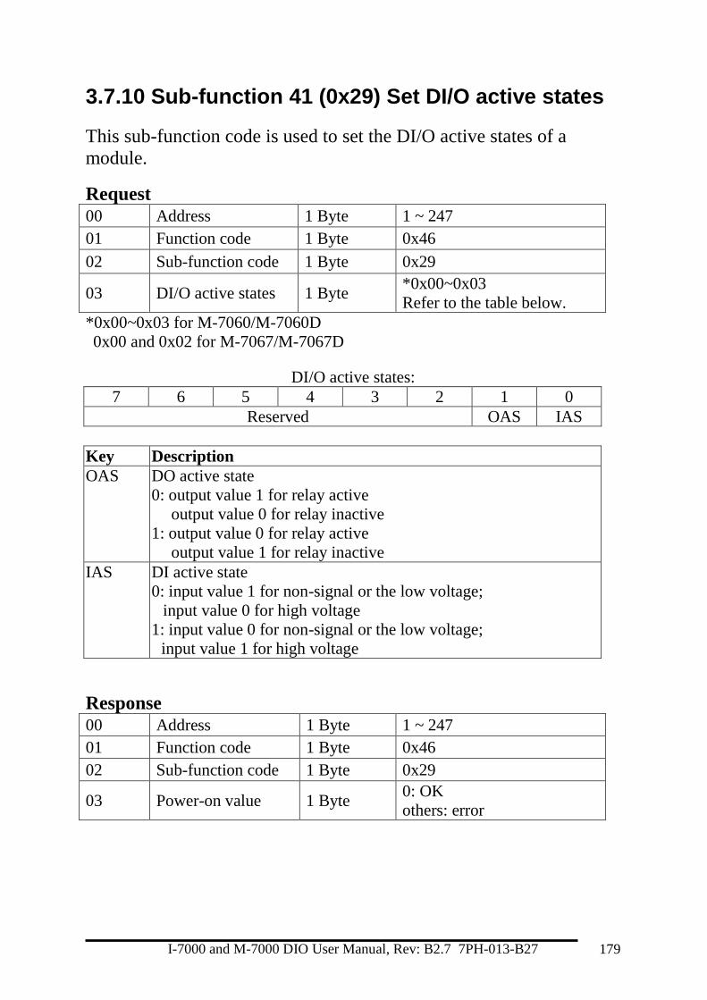
I-7000 and M-7000 DIO User Manual, Rev: B2.7 7PH-013-B27 179
3.7.10 Sub-function 41 (0x29) Set DI/O active states
This sub-function code is used to set the DI/O active states of a
module.
Request
00 Address 1 Byte 1 ~ 247
01 Function code 1 Byte 0x46
02 Sub-function code 1 Byte 0x29
03 DI/O active states 1 Byte *0x00~0x03
Refer to the table below.
*0x00~0x03 for M-7060/M-7060D
0x00 and 0x02 for M-7067/M-7067D
DI/O active states:
7 6 5 4 3 2 1 0
Reserved OAS IAS
Key Description
OAS DO active state
0: output value 1 for relay active
output value 0 for relay inactive
1: output value 0 for relay active
output value 1 for relay inactive
IAS DI active state
0: input value 1 for non-signal or the low voltage;
input value 0 for high voltage
1: input value 0 for non-signal or the low voltage;
input value 1 for high voltage
Response 00 Address 1 Byte 1 ~ 247
01 Function code 1 Byte 0x46
02 Sub-function code 1 Byte 0x29
03 Power-on value 1 Byte 0: OK
others: error

I-7000 and M-7000 DIO User Manual, Rev: B2.7 7PH-013-B27 180
Error Response 00 Address 1 Byte 1 ~ 247
01 Function code 1 Byte 0xC6
02 Exception code 1 Byte Refer to the Modbus standard for
more details.
Supported Modules
M-7060/M-7060D/M-7064/M-7064D/M-7067/M-7067D/M-7050/M-
7050D/M-7051/M-7051D/M-7052/M-7052D/M-7053/M-7053D/M-
7054/M-7054D/M-7055/M-7055D/ M-7055U/M-7055UD/M-
7041/M-7041D/M-7043/M-7043D/M-7045/M-7045D/M-7046/M-
7046D
Note: After using the command, the DIO active states will immediately change
and will simultaneously clear the DI counter and latch values.
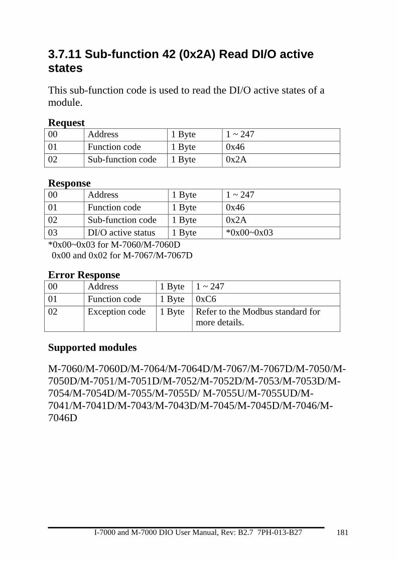
I-7000 and M-7000 DIO User Manual, Rev: B2.7 7PH-013-B27 181
3.7.11 Sub-function 42 (0x2A) Read DI/O active states
This sub-function code is used to read the DI/O active states of a
module.
Request 00 Address 1 Byte 1 ~ 247
01 Function code 1 Byte 0x46
02 Sub-function code 1 Byte 0x2A
Response 00 Address 1 Byte 1 ~ 247
01 Function code 1 Byte 0x46
02 Sub-function code 1 Byte 0x2A
03 DI/O active status 1 Byte *0x00~0x03
*0x00~0x03 for M-7060/M-7060D
0x00 and 0x02 for M-7067/M-7067D
Error Response 00 Address 1 Byte 1 ~ 247
01 Function code 1 Byte 0xC6
02 Exception code 1 Byte Refer to the Modbus standard for
more details.
Supported modules
M-7060/M-7060D/M-7064/M-7064D/M-7067/M-7067D/M-7050/M-
7050D/M-7051/M-7051D/M-7052/M-7052D/M-7053/M-7053D/M-
7054/M-7054D/M-7055/M-7055D/ M-7055U/M-7055UD/M-
7041/M-7041D/M-7043/M-7043D/M-7045/M-7045D/M-7046/M-
7046D
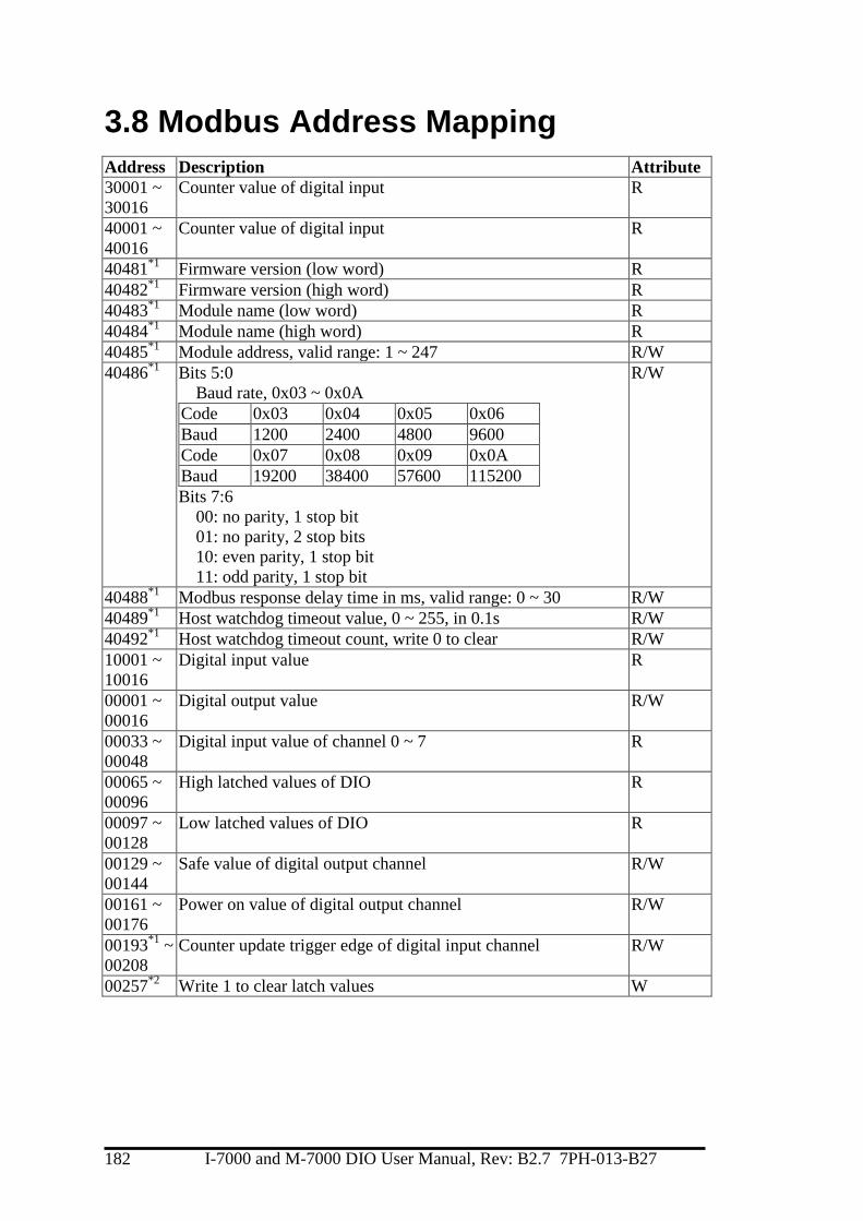
I-7000 and M-7000 DIO User Manual, Rev: B2.7 7PH-013-B27 182
3.8 Modbus Address Mapping
Address Description Attribute
30001 ~
30016
Counter value of digital input R
40001 ~
40016
Counter value of digital input R
40481*1
Firmware version (low word) R
40482*1
Firmware version (high word) R
40483*1
Module name (low word) R
40484*1
Module name (high word) R
40485*1
Module address, valid range: 1 ~ 247 R/W
40486*1
Bits 5:0
Baud rate, 0x03 ~ 0x0A
Code 0x03 0x04 0x05 0x06
Baud 1200 2400 4800 9600
Code 0x07 0x08 0x09 0x0A
Baud 19200 38400 57600 115200
Bits 7:6
00: no parity, 1 stop bit
01: no parity, 2 stop bits
10: even parity, 1 stop bit
11: odd parity, 1 stop bit
R/W
40488*1
Modbus response delay time in ms, valid range: 0 ~ 30 R/W
40489*1
Host watchdog timeout value, 0 ~ 255, in 0.1s R/W
40492*1
Host watchdog timeout count, write 0 to clear R/W
10001 ~
10016
Digital input value R
00001 ~
00016
Digital output value R/W
00033 ~
00048
Digital input value of channel 0 ~ 7 R
00065 ~
00096
High latched values of DIO R
00097 ~
00128
Low latched values of DIO R
00129 ~
00144
Safe value of digital output channel R/W
00161 ~
00176
Power on value of digital output channel R/W
00193*1
~
00208
Counter update trigger edge of digital input channel R/W
00257*2
Write 1 to clear latch values W

I-7000 and M-7000 DIO User Manual, Rev: B2.7 7PH-013-B27 183
Address Description Attribute
00257*1
Protocol, 0: DCON, 1: Modbus RTU R/W
00258*1
0: Modbus RTU, 1: Modbus ASCII R/W
00260*1
Modbus host watchdog mode
0: same as I-7000
1: can use write DO command to clear host
watchdog timeout status
R/W
00261*1
1: enable, 0: disable host watchdog R/W
00264*1
Write 1 to clear latched DIO W
00265*1
DI active state, 0: normal, 1: inverse R/W
00266*1
DO active state, 0: normal, 1:inverse R/W
00270*1
Host watch dog timeout status, write 1 to clear host
watch dog timeout status
R/W
00273*1
Reset status, 1: first read after powered on, 0: not
the first read after powered on
R
00513 ~
00528
Write 1 to clear counter value of digital input
channel
W
Note:
*1: only available with firmware version 200 and later
*2: only available with firmware version 199 and earlier

I-7000 and M-7000 DIO User Manual, Rev: B2.7 7PH-013-B27 184
4. Troubleshooting
If you are having difficulty using the I-7000 or M-7000
module, here are some suggestions that may help. If you
cannot find the answers you need in these guides, contact ICP
DAS Product Support. Contact information is located in
Section 1.14.

I-7000 and M-7000 DIO User Manual, Rev: B2.7 7PH-013-B27 185
4.1 Communicating with the module
If you attempt to communicate with the module and receive
no response, first check the following:
Ensure that the supplied power is within the range of +10
to +30 V DC. If the supplied power is OK, then the power
LED should be on.
When the module receives a command, the power LED is
set to “off”. The power LED is shown as “on” after the
module responds. This method can be used to check
whether the module has received a command sent from the
host.
If possible, use another device to check whether the host
can communicate with the device through the same RS-
485 network.
If the host is a PC installed with a Windows operating
system, then execute the DCON Utility to determine
whether the module can be found. The DCON Utility can
be downloaded from the ICP DAS website
http://www.icpdas.com. The DCON Utility
documentation can be found in the ”Getting Started For
I-7000 Series Modules” manual.
Set the module to “INIT mode” and communicate with the
module using the following settings: address 00, Baud
Rate 9600bps and no checksum. See Section A.1 for
details.

I-7000 and M-7000 DIO User Manual, Rev: B2.7 7PH-013-B27 186
A. Appendix A.1 INIT Mode
Each I-7000 and M-7000 module has a built-in EEPROM to
store configuration information such as module address, type
code, Baud Rate, etc. Occasionally, the configuration of a
module may be forgotten and there are no visual indications
of the configuration of the module. It is difficult to
communicate with the module when the configuration of the
module is unknown. To help avoid this problem, the I-7000
and M-7000 series has a special mode called “INIT mode”.
When the module is powered on in “INIT mode” the
configuration of the module is reset as follows, allowing it to
be operated as normal.
1. Address: 00
2. Baud Rate: 9600 bps
3. No checksum
4. Protocol: DCON
The configuration information stored in the EEPROM is not
changed and can be read by sending the $002(CR) command
at 9600bps.
There are commands that require the module to be in INIT
mode. They are:
1. %AANNTTCCFF when changing the Baud Rate and
checksum settings. See Section 2.1 for details.
2. $AAPN, see Section 2.20 for details.
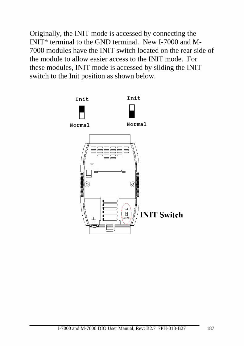
I-7000 and M-7000 DIO User Manual, Rev: B2.7 7PH-013-B27 187
Originally, the INIT mode is accessed by connecting the
INIT* terminal to the GND terminal. New I-7000 and M-
7000 modules have the INIT switch located on the rear side of
the module to allow easier access to the INIT mode. For
these modules, INIT mode is accessed by sliding the INIT
switch to the Init position as shown below.
I-7000 and M-7000 DIO User Manual, Rev: B2.7 7PH-013-B27 188
A.2 Dual Watchdog Operation
Dual Watchdog = Module Watchdog + Host Watchdog
The Module Watchdog is a hardware reset circuit that
monitors the operating status of the module. While working
in harsh or noisy environments, the module may be shut down
by external signals. The circuit allows the module to work
continuously without disruption.
The Host Watchdog is a software function that monitors the
operating status of the host. Its purpose is to prevent
problems due to network/communication errors or host
malfunctions. When a host watchdog timeout occurs, the
module will reset all outputs to a safe state in order to prevent
any erroneous operations of the controlled target.
I-7000 and M-7000 series modules include an internal Dual
Watchdog, making the control system more reliable and
stable.
For more information regarding the Dual Watchdog, please
refer to Chapter 5 of the “Getting Started For I-7000 Series
Modules” manual that can be downloaded from the ICP DAS
website http://www.icpdas.com.

I-7000 and M-7000 DIO User Manual, Rev: B2.7 7PH-013-B27 189
A.3 Frame Ground
Electronic circuits are constantly vulnerable to Electro-Static
Discharge (ESD), which become worse in a continental
climate area. Some I-7000 and M-7000 modules feature a
new design for the frame ground, which provides a path for
bypassing ESD, allowing enhanced static protection (ESD)
capability and ensures that the module is more reliable.
Either of the following options will provide a better protection
for the module:
1. If the module is DIN rail mounted, connect the DIN rail to
the earth ground because the DIN rail is in contact with the
upper frame ground as shown in the figure below.
2. Alternatively, connect the lower frame ground terminal to
a wire and connect the wire to the earth ground, as shown
in the figure below.

I-7000 and M-7000 DIO User Manual, Rev: B2.7 7PH-013-B27 190
New DIN rail models are available that can easily be
connected to the earth ground. Each is made of stainless steel,
which is stronger than those made of aluminum. There is a
screw at one end and a ring terminal is included as shown in
the figure below. Refer to Section 1.13.1 for more
information about the new DIN rail models.

I-7000 and M-7000 DIO User Manual, Rev: B2.7 7PH-013-B27 191
A.4 Reset Status
The reset status of a module is set when the module is
powered-on or when the module is reset by the module
watchdog. It is cleared after the responding of the first $AA5
command. This can be used to check whether the module had
been reset. When the $AA5 command responds that the reset
status is cleared, that means the module has not been reset
since the last $AA5 command was sent. When the $AA5
command responds that the reset status is set and it is not the
first time $AA5 command is sent, it means the module has
been reset and the digital output value had been changed to
the power-on value.
I-7000 and M-7000 DIO User Manual, Rev: B2.7 7PH-013-B27 192
A.5 Safe Value and Power-on Value of Digital Output
Besides setting by the set digital output commands, the digital
outputs can be set under two other conditions.
When the host watchdog is enabled and a host watchdog
timeout occurs, the “safe value” is loaded into the digital
output ports. The set digital output commands have no effect
on the digital output ports until the host watchdog timeout
status is cleared. The host watchdog timeout status is saved in
the EEPROM. The status is not changed even after power-on
reset. It can be cleared only by the reset host watchdog
timeout status command ~AA1. See Section A.2 for host
watchdog details.
When the module is powered on and the host watchdog
timeout status is cleared, the “power-on value” is loaded into
the digital output ports. If the host watchdog timeout status is
not cleared on power-on, then the safe value is loaded into the
digital output ports.
Both the safe value and power-on value are set by the ~AA5V
command. Refer to Section 2.30 for details.

I-7000 and M-7000 DIO User Manual, Rev: B2.7 7PH-013-B27 193
A.6 Latched Digital Input
The I-7000 and M-7000 DIO modules provide commands to
read the latched high digital input and latched low digital
input status. Following is an example to show the usefulness
of the latched digital input. When we want to read the key
stroke of a key switch connected to the digital input channel
of a module, the input signal of the key stroke is a pulse signal
as shown in the following figure.
If we just use the read digital input status command to read
the signal and we cannot send the command during the B
period due to some reasons, then we will lose the key stroke
information. However, with the read latched digital input
command, we can still get the key stroke information even we
are not able to send command in B period. For details of the
read latched digital input command, please refer to Sections
2.17 and 3.1.

I-7000 and M-7000 DIO User Manual, Rev: B2.7 7PH-013-B27 194
A.7 DN Module
The DN modules are the I/O extension of the I-7000 and
M-7000 modules. They can drive more power and heavy load.
User may use I-7000 and M-7000 modules to control the DN
modules to drive the loads. Following is an example of using
the I-7043 with the DN module.
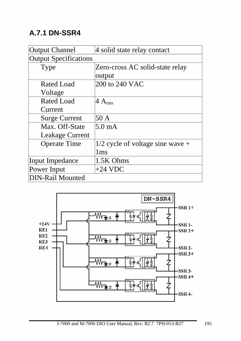
I-7000 and M-7000 DIO User Manual, Rev: B2.7 7PH-013-B27 195
A.7.1 DN-SSR4
Output Channel 4 solid state relay contact
Output Specifications
Type Zero-cross AC solid-state relay
output
Rated Load
Voltage
200 to 240 VAC
Rated Load
Current
4 Arms
Surge Current 50 A
Max. Off-State
Leakage Current
5.0 mA
Operate Time 1/2 cycle of voltage sine wave +
1ms
Input Impedance 1.5K Ohms
Power Input +24 VDC
DIN-Rail Mounted

I-7000 and M-7000 DIO User Manual, Rev: B2.7 7PH-013-B27 196
A.7.2 DN-PR4
Output Channel 4 relay contact
Output Specifications
Type 1 Form C relay contact
Nominal Load 5A@250VAC, 5A@30VDC
Max. Switching Power 1250 VA
Max. Switching Voltage 250 VAC, 150 VDC
Max. Switching Current 5 A
Mechanical Life 10 x 106 operations min.
Electric Life 100 x 103 operations min.
Operate/Release Time Max. 10 ms / 5 ms
Dielectric Strength 2000 VAC 1 minute
Nominal Coil Power 360 mW
Power Input +24 VDC
DIN-Rail Mounted

I-7000 and M-7000 DIO User Manual, Rev: B2.7 7PH-013-B27 197
A.7.3 RM-104, RM-108, and RM-116
Output Channel 4/8/16 relay contact
Output Specifications
Type 1 Form C relay contact
Rated Load 16A@250VAC
Max. Switching Voltage 400 VAC
Max. Peak Current 30 A
Contact Material AgCdO
Min. Life 100,000 operations
Dimensions
RM-104 78 mm x 77 mm
RM-108 135 mm x 77 mm
RM-116 270 mm x 77 mm
Power Input +24 VDC
DIN-Rail Mounted
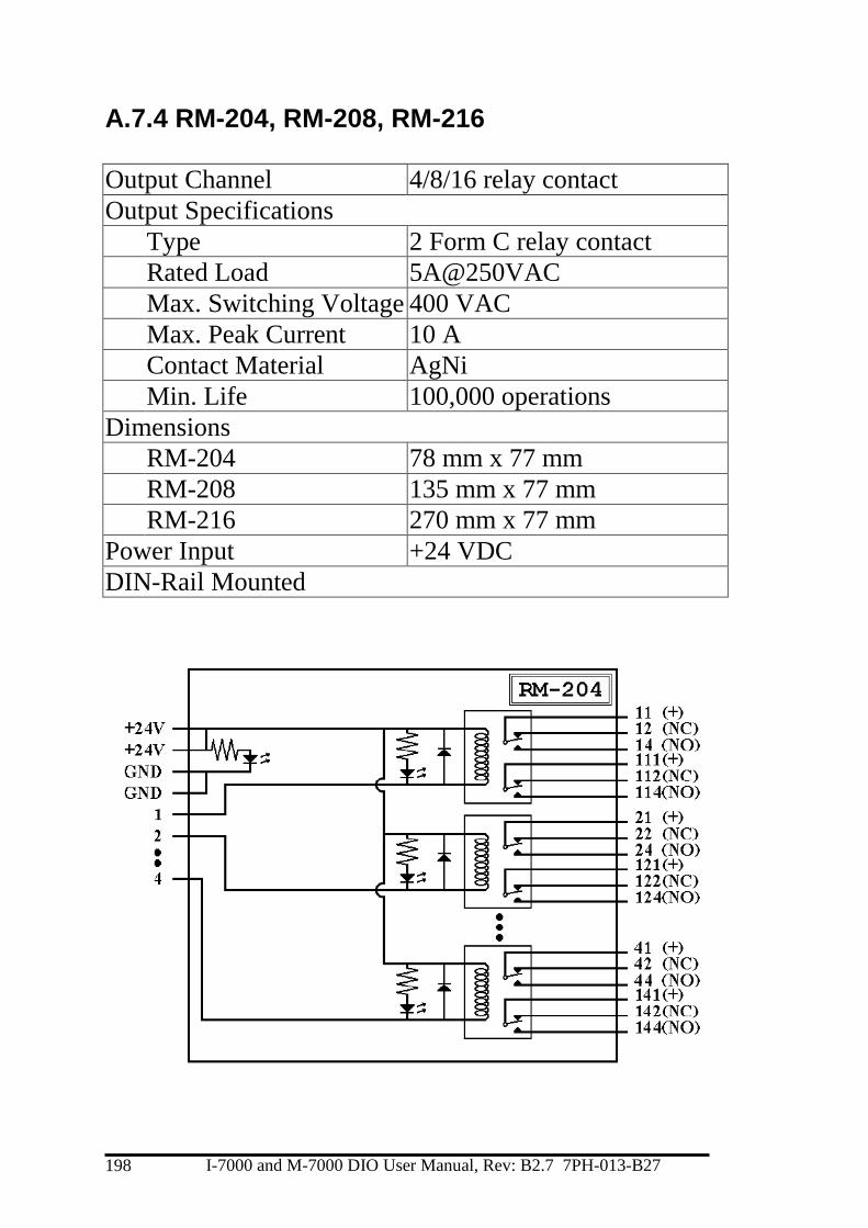
I-7000 and M-7000 DIO User Manual, Rev: B2.7 7PH-013-B27 198
A.7.4 RM-204, RM-208, RM-216
Output Channel 4/8/16 relay contact
Output Specifications
Type 2 Form C relay contact
Rated Load 5A@250VAC
Max. Switching Voltage 400 VAC
Max. Peak Current 10 A
Contact Material AgNi
Min. Life 100,000 operations
Dimensions
RM-204 78 mm x 77 mm
RM-208 135 mm x 77 mm
RM-216 270 mm x 77 mm
Power Input +24 VDC
DIN-Rail Mounted