I 11111 111111ll111 Ill11 Ill11 IIIII IIIII IIIII 11111 ...
22
I 11111 111111 l l 111 I l l 11 I l l 11 IIIII IIIII IIIII 11111 Il11 111 l 111111111111111111 US006157037A United States Patent [19] [ill Patent Number: 6,157,037 Danielson [45] Date of Patent: Dec. 5,2000 SENSING DEVICE AND METHOD FOR MEASURING EMISSION TIME DELAY DURING IRRADIATION OF TARGETED SAMPLES Inventor: J. D. Sheldon Danielson, Boulder, Colo. Assignee: Photosense, LLC, Boulder, Colo. Appl. No.: 09/205,755 Filed: Dec. 4, 1998 Int. C1.7 ..................................................... GOlN 21/64 U.S. C1. ..................................... 250/458.1; 2501459.1; 3561318 Field of Search .............................. 2501458.1, 459.1, 2501461.1; 3561318, 417; 4361172 References Cited 4,716,363 4,840,485 4,845,368 5,196,709 5,212,386 5,257,202 5,317,162 5,424,843 5,462,879 5,485,530 5,495,850 5,504,337 5,515,864 5,610,716 5,624,847 5,626,134 5,633,712 5,646,734 5,671,301 5,757,013 5,818,582 U.S. PATENT DOCUMENTS 1211987 Dukes et al. .............................. 324177 611989 Gratton ................................... 3561317 711989 Demas et al. 311993 Berndt et al. 511993 Gratton et al. ..... 511994 Pinsky et al. ...... 1011993 Fedderson et al. 611995 Tromberg et al. ...................... 3561442 1011995 Bentson .................................. 4361136 111996 Lakowicz et 311996 Zuckerman 511996 Zuckerman 311997 Sorin et al. 511997 Zuckerman ........ 511997 Venkatesh et al. 911997 Kupershmidt ............................... 38511 511998 Groger et al. 2501458.1 1011998 Fernandez et al. ..................... 3561318 OTHER PUBLICATIONS A closed loop scheme for phase-sensitive flurometry, Apr. 14, 1995, Venkatesh Vadde and Vivek Strinivas, Indian Institute of Science, Department of Electrical Communica- tion Engineering, Bangalore, India pp. 1-5. Digital parallel acquisition in frequency domain florimetry, Sep., 1989, Brett A Federson, David W. Piston, and Enrico Gratton, Department of Physics, University of Illinois at Urbana-Champaign, Urbana, Illinois pp. 1-8. Primary ExarninerSeungsook Ham Assistant Examinerqichard Hanig Attorney, Agent, or Firm-John L. Isaac; Isaac &Associates [571 ABSTRACT An apparatus for measuring emission time delay during irradiation of targeted samples by utilizing digital signal processing to determine the emission phase shift caused by the sample is disclosed. The apparatus includes a source of electromagnetic radiation adapted to irradiate a target sample. A mechanism generates first and second digital input signals of known frequencies with a known phase relationship, and a device then converts the first and second digital input signals to analog sinusoidal signals. An element is provided to direct the first input signal to the electromag- netic radiation source to modulate the source by the fre- quency thereof to irradiate the target sample and generate a target sample emission. A device detects the target sample emission and produces a corresponding first output signal having a phase shift relative to the phase of the first input signal, the phase shift being caused by the irradiation time delay in the sample. Amember produces a known phase shift in the second input signal to create a second output signal. A mechanism is then provided for converting each of the first and second analog output signals to digital signals. A mixer receives the first and second digital output signals and compares the signal phase relationship therebetween to produce a signal indicative of the change in phase relation- ship between the first and second output signals caused by the target sample emission. Finally, a feedback arrangement alters the phase of the second input signal based on the mixer signal to ultimately place the first and second output signals in quadrature. Mechanisms for enhancing this phase com- parison and adjustment technique are also disclosed. 26 Claims, 6 Drawing Sheets
Transcript of I 11111 111111ll111 Ill11 Ill11 IIIII IIIII IIIII 11111 ...
I 11111 111111ll111 Ill11 Ill11 IIIII IIIII IIIII 11111 Ill11 111ll111111111111111111 US006157037A
United States Patent [19] [ i l l Patent Number: 6,157,037 Danielson [45] Date of Patent: Dec. 5,2000
SENSING DEVICE AND METHOD FOR MEASURING EMISSION TIME DELAY DURING IRRADIATION OF TARGETED SAMPLES
Inventor: J. D. Sheldon Danielson, Boulder, Colo.
Assignee: Photosense, LLC, Boulder, Colo.
Appl. No.: 09/205,755
Filed: Dec. 4, 1998
Int. C1.7 ..................................................... GOlN 21/64 U.S. C1. ..................................... 250/458.1; 2501459.1;
3561318 Field of Search .............................. 2501458.1, 459.1,
2501461.1; 3561318, 417; 4361172
References Cited
4,716,363 4,840,485 4,845,368 5,196,709 5,212,386 5,257,202 5,317,162 5,424,843 5,462,879 5,485,530 5,495,850 5,504,337 5,515,864 5,610,716 5,624,847 5,626,134 5,633,712 5,646,734 5,671,301 5,757,013 5,818,582
U.S. PATENT DOCUMENTS
1211987 Dukes et al. .............................. 324177 611989 Gratton ................................... 3561317 711989 Demas et al. 311993 Berndt et al. 511993 Gratton et al. .....
511994 Pinsky et al. ...... 1011993 Fedderson et al.
611995 Tromberg et al. ...................... 3561442 1011995 Bentson .................................. 4361136 111996 Lakowicz et 311996 Zuckerman
511996 Zuckerman 311997 Sorin et al.
511997 Zuckerman ........ 511997 Venkatesh et al.
911997 Kupershmidt ............................... 38511 511998 Groger et al. 2501458.1
1011998 Fernandez et al. ..................... 3561318
OTHER PUBLICATIONS
A closed loop scheme for phase-sensitive flurometry, Apr. 14, 1995, Venkatesh Vadde and Vivek Strinivas, Indian Institute of Science, Department of Electrical Communica- tion Engineering, Bangalore, India pp. 1-5. Digital parallel acquisition in frequency domain florimetry, Sep., 1989, Brett A Federson, David W. Piston, and Enrico Gratton, Department of Physics, University of Illinois at Urbana-Champaign, Urbana, Illinois pp. 1-8.
Primary ExarninerSeungsook Ham Assistant Examinerqichard Hanig Attorney, Agent, or Firm-John L. Isaac; Isaac &Associates
[571 ABSTRACT
An apparatus for measuring emission time delay during irradiation of targeted samples by utilizing digital signal processing to determine the emission phase shift caused by the sample is disclosed. The apparatus includes a source of electromagnetic radiation adapted to irradiate a target sample. A mechanism generates first and second digital input signals of known frequencies with a known phase relationship, and a device then converts the first and second digital input signals to analog sinusoidal signals. An element is provided to direct the first input signal to the electromag- netic radiation source to modulate the source by the fre- quency thereof to irradiate the target sample and generate a target sample emission. A device detects the target sample emission and produces a corresponding first output signal having a phase shift relative to the phase of the first input signal, the phase shift being caused by the irradiation time delay in the sample. Amember produces a known phase shift in the second input signal to create a second output signal. A mechanism is then provided for converting each of the first and second analog output signals to digital signals. A mixer receives the first and second digital output signals and compares the signal phase relationship therebetween to produce a signal indicative of the change in phase relation- ship between the first and second output signals caused by the target sample emission. Finally, a feedback arrangement alters the phase of the second input signal based on the mixer signal to ultimately place the first and second output signals in quadrature. Mechanisms for enhancing this phase com- parison and adjustment technique are also disclosed.
26 Claims, 6 Drawing Sheets

U S . Patent Dec. 5,2000 Sheet 1 of 6 6,157,037
rL
I
e T
U S . Patent Dec. 5,2000 Sheet 2 of 6
c\1 co c
4 )
-57,037
L

U S . Patent Dec. 5,2000 Sheet 3 of 6 6,157,037
cv CD
i
0 03
L L
(D m
cv 03
3 I 5:
Y 8 1 a cv
I 1 I
8 N d
N
eo a
I I m I (0
0

U S . Patent Dec. 5,2000 Sheet 4 of 6 6,157,037
1
co N 8 s cn
I I F
W 52
LN 0)
I I I i I
a3 m d
N a3 0
N d
I d d

U S . Patent Dec. 5,2000
e 2 " i ii
v)
1
10,
Sheet 5 of 6 6,157,037
%------- I

U S . Patent
0 0 cu
I
Dec. 5,2000 Sheet 6 of 6 6,157,037
\ r------i---l
0 T J
t c? E cu 0 1 - - .- - - - + - - 4- -
.t cu
r t r I
W 0 cu I
3 W (v cu cv
I cu M
; I
d- 0 cv
6,157,037 2 1
SENSING DEVICE AND METHOD FOR MEASURING EMISSION TIME DELAY
DURING IRRADIATION OF TARGETED SAMPLES
CONTRACTUAL ORIGIN OF THE INVENTION
This invention was made with U.S. Government support under contract NAS9-97080 awarded by NASA and contract F33615-97-0729 awarded by the Department of the Air Force. The Government has certain rights in this invention.
BACKGROUND OF THE INVENTION
1. Field of the Invention This invention relates generally to sensing instruments
and methods for measuring the concentration of an analyte in a medium and, more particularly, to a device and method for measuring such concentrations by measuring the emis- sion time delay during irradiation of a targeted sample surrounded by the analyte. Specifically, the present inven- tion relates to a device and method for measuring exponen- tial time constants, phase shifts, time delays and parameters derivable therefrom caused by irradiation of a targeted sample utilizing digital signal processing and especially luminescence quenching systems, phase shifts through networks, and time delays of photon migration through media.
2. Description of the Prior Art Dynamic phase modulation, quenched luminescence sen-
sors are well known. Instruments of this type have been, for example, developed or proposed for use in hospitals to monitor the concentration of gases such as oxygen, ionized hydrogen and carbon dioxide within the blood of patients. The particular substance of interest, for example oxygen, is known as the analyte.
As is known in the art, luminescence materials absorb energy and are driven from their ground state energy level to an excited state energy level in response to the application of energy from an electromagnetic radiation source such as light. These materials are unstable in their excited states, and they luminesce or give off excess energy as they return to their ground state. For example, the short wavelength ultra- violet light of black light stimulates dyes in a colored fabric to emit longer wavelengths, such as blue, green or red, and thus fluoresce. For the purposes of the present disclosure, the term “luminescence” as used herein is a general term which describes both fluorescence and phosphorescence, for all three terms are frequently used interchangeably in the art. The distinction and overlap of the terms is obvious to one skilled in the art.
In the presence of certain chemicals, many fluorescent materials are said to be quenched, i.e. the time constant of the fluorescence emission is altered by the effects of the surrounding chemicals. The degree of quenching of the fluorescence in turn can be related to the concentration of the quencher, which for example may be a chemical dissolved in water or mixed in air, such as oxygen in the blood of patients as explained above. There is a substantial amount of literature that describes fluorescent molecules that are selec- tively quenched by oxygen, carbon dioxide, glucose, pH, NH,, metal ions, temperature and other environmentally and medically important analytes. These analytes are relevant to applications such as monitoring drinking water quality, industrial process control, monitoring of human respiratory function, human blood analysis for critical care patients, and the like.
One of the obstacles to the commercialization of fluores- cence sensing devices has been a lack of inexpensive yet accurate instrumentation for the measurement of changes in the fluorescent time constant. For example, U.S. Pat. Nos.
s 4,845,368, 5,257,202, 5,495,850, 5,515,864 and 5,626,134 all disclose devices for measuring analyte concentration levels based on fluorescence. However, these particular devices are generally expensive and complicated.
The fluorescence lifetime or time constant, z, is the 10 amount of time it takes the fluorescence emission to
decrease by a factor of l ie or about 63% after termination of irradiation as disclosed in U.S. Pat. No. 4,716,3632 by Dukes et al, in column 1, lines 37-41. This is common knowledge and is available in the literature reference, i.e.
15 “Topics in Fluorescence Vol. 2-Principles”, ed. Joseph Lakowicz. If light modulated sinusoidally at a frequency, f, is thus applied to the fluorescence sensor, the output is a sinusoidal emission of identical frequency, but having a phase shift and reduced amplitude with respect to the
20 excitation signal. The equation governing the relationship between modulation frequency, f, phase shift, 8, and the fluorescent time constant, z, is as follows:
tan e (Equation 1) T = - or Barctan(2ir f T)
2s kf
Thus, if we know the excitation modulation frequency and can measure the phase shift of the emission signal
30 relative to the excitation signal, we can determine the fluorescence constant, z, using the above Equation 1. In a fluorescence-based sensor, the fluorescence time constant is measured since this fluorescence time constant is altered by the presence of certain chemical species. Consequently, the
35 concentration of chemical species can be determined by measuring the fluorescence time constant by measuring the phase shift associated therewith.
According to Equation 1, in order to measure the fluo- rescence time constant, one must know the excitation modu-
40 lation frequency, f, and the phase shift of the light through the fluorescence system. With these quantities, the fluores- cence time constant can be calculated and then related to analyte concentration. There are several different known techniques for determining the excitation frequency and
4s phase shift of a system with an unknown time constant. One manner of determining this is by exciting the sample with a fixed frequency signal and then measuring the phase shift that results, that is the sample excitation modulation fre- quency is maintained constant while the signal phase, which
so varies with analyte concentration, is measured. U.S. Pat. Nos. 5,317,162, 5,462,879, 5,485,530 and 5,504,337 all disclose such fixed frequency, variable phase techniques and devices. Of particular interest is an article by Venkatesh Vadde and Vivek Srinivas entitled, “A closed loop scheme
ss for phase-sensitive fluorometry”, the American Institute of Physics, Rev. Sci. Instrum., Vol. 66, No. 7, July 1995, p. 3750.
Another principal way of conducting the above measure- ments is by exciting the sample with a modulation frequency
60 that maintains a constant phase relationship between the excitation signal and the emission signal, that is the excita- tion frequency is varied in order to maintain a particular phase relationship. Such devices and techniques are known as phase-modulation, fluorescence-based sensing devices
65 and are clearly illustrated in U.S. Pat. Nos. 4,840,485, 5,196,709, and 5,212,386, and in an article by Brett A. Feddersen, et al. entitled, “Digital parallel acquisition in
6,157,037 3 4
frequency domain fluorimetry", American Institute of with a known variable phase relationship, and a device then Physics, Rev. Sci. lnstrum., Vol. 60, No. 9, September 1989, converts the first and second digital input signals to analog p. 2929. Of particular interest is U.S. Pat. No. 4,716,3632 by sinusoidal signals. An element is provided to direct the first Dukes et al., which describes a feedback system that pro- input signal to the electromagnetic radiation source to modu- vides the modulation frequency required to give a constant s late the source by the frequency thereof to irradiate the target phase shift of about 45". The resulting frequency is then sample and generate a target sample emission. A device used to determine the analyte concentration which is a detects the target sample emission and produces a corre- function of excited state lifetime. sponding first output signal having a phase shift relative to
U.S. Pat. No. 5,818,582 teaches the use of a DSP for the Phase of the first input signal, the Phase shift being fluorescence lifetime measurements, though not using 10 caused by the emission time delay in the sample. Amember quadrature signal comparison for determination of fluores- Produces a known Phase shift in the second input signal to cent sample phase shifts. create a second output signal. Amechanism is then provided
and sensing devices, there is a continuing need for improved signals to digital signals. A mixer receives the first and
is a need for such devices which are useful for a broad range relationship therebetween to produce a signal indicative of of applications involving exponential decay and time delay the change in phase relationship between the first and second measurements, which are made from inexpensive output signals caused by the target sample emission. Finally,
without the need for off-line signal processing as is the 20 signal based on the mixer signal to ultimately place the first
Despite the availability of the above-discussed techniques for converting each Of the first and second Output
fluorescence-based sensing instruments. In particular, there 1s second digital output signals and compares the signal Phase
components, and which present measurements in real time
of the patents to Federson, Gratton and others. A major detriment to many of the devices presently available is that
a feedback arrangement the phase Of the second hut
and second Output in quadrature. Mechanisms for enhancing this Phase comparison and adjustment technique
they are very expensive to acquire and maintain. Moreover, analog systems of the present art are subject to drift and therefore unnecessary errors. Such systems should be, to the 2s contrary, inexpensive, convenient to use and Provide adequate sensitivity over an extended and continuous mea- surement range. The system of the Dukes Patent emphasizes optimal sensitivity over a wide measurement range, but in so doing, requires very complex and expensive system com- 30 ponents. To the contrary, optimal sensitivity can be sacri-
are
BRIEF DESCRIPTION OF THE DRAWINGS
The accompanying drawings which are incorporated in and form a part of the specification illustrate preferred embodiments of the present invention and, together with a description, Serve to explain the principles of the invention,
is a schematic illustrating an embodiment of the the drawings: FIG,
ficed for sub-optimal, adequate sensitivity in Order to present invention utilizing a direct phase adjustment, con- achieve inexpensive, less measurement tech- stant frequency technique with digital signal processing for niques. In addition, the measurement approach Of such 3s measuring emission phase shift to determine tirne delay devices should be susceptible to convenient and precise readout.
through an irradiated sample, FIG. 2 is a schematic illustrating another embodiment of
SUMMARY OF THE INVENTION the present invention utilizing variable-frequency and variable-phase techniques for measuring emission phase
40 shift to determine time delay through an irradiated sample. FIG. 3 is a schematic illustrating yet another embodiment
of the present invention similar to that of FIG. 2 but incorporating
FIG. 4 is a schematic illustrating yet another embodiment and various scattering 4s of the present invention similar to that of FIG. 3 but
incorporating dual quadrature signal down conversion steps. FIG. 5 is a schematic illustrating yet another embodiment
of the present invention similar to that of FIG. 4 but eliminating the means for the downconverting of high frequency signals to lower frequencies for quadrature Phase detection.
FIG. 6 is a schematic illustrating yet another embodiment of the present invention using a single analog timing element
ss and a DSP for real time determination of phase and lifetime.
Accordingly, it is one object of the present invention to provide an apparatus and method for measuring emission time delay during irradiation of targeted samples.
It is another object of the present invention to provide sensing instruments which are applicable to a broad range tirne delay, phase shift and exponential decay measurements involving luminescent media.
down conversion steps.
Yet another object of the present invention is to provide fluorescence-based sensing instruments which are made from inexpensive components.
Still another object of the present invention is to provide an apparatus and method for measuring emission time delay during irradiation of targeted samples utilizing digital signal processing to determine the emission phase shift caused by the sample.
so
A further object of the present invention is to provide an apparatus and method for measuring luminescence- quenching systems, specifically oxygen sensitive systems.
DETAILED DESCRIPTION OF THE PREFERRED EMBODIMENTS
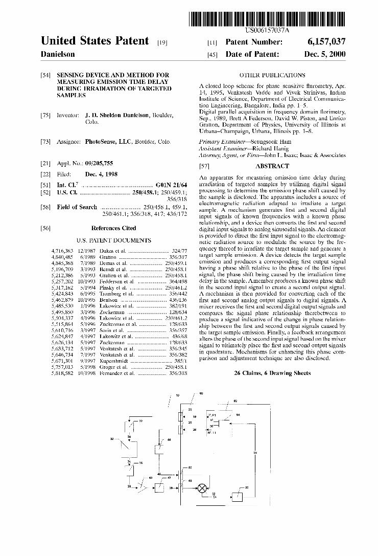
To achieve the foregoing and other objects and in accor- Referring initially to FIG. 1, a closed-loop lifetime mea- dance with the purpose of the present invention, as embod- 60 surement device 10 is illustrated which incorporates a Digi- ied and broadly described herein, an apparatus is disclosed tal Signal Processor (DSP) 12. Venkatesh and Srinivas, in for measuring emission time delay during irradiation of the prior art references discussed above, disclose a closed- targeted samples by utilizing digital signal processing to loop fluorescent-decay time measurement system that determine the emission phase shift caused by the sample. allows a phase demodulator to operate in an optimal null The apparatus includes a source of electromagnetic radiation 65 condition. This is accomplished using two analog timing adapted to irradiate a target sample. A mechanism generates elements including a crystal-controlled frequency generator first and second digital input signals of known frequencies and a second analog timing element to vary the phase of a

6,157,037 5 6
measurement reference signal so that signals to the demodu- 26 are out-of-phase by a known, predetermined amount. lator are always in quadrature. An important aspect of this However, due to the phase shift imposed by the target disclosed technique is that the reference channel is phase sample 32, the phase differences between the output signals advanced in order to maintain quadrature at the phase 38 and 46 at the mixing member 52 are unknown. Therefore demodulator. 5 and in preferred form, the phase demodulator 52 indicates
Within the DSP 12 of FIG. 1, all the components referred when the reference signal 46 (A) relative to the experimental to below are digital and defined by software loaded into the signal 38 (B) are in quadrature, or 90" apart. In other words, DSP chip. In the DSP 12, a constant frequency, dual-output, 9O0-B=A if the signals are in quadrature. If the signals 38 variable-phase waveform generator 14 is provided and and 46 are in fact in quadrature, then no changes are made adapted to generate a first experimental digital signal 16 and to the relative phase offset between input signals 16 and 26. a second reference digital signal 26. The digital signals 16, However, due to the phase shift caused by the target sample 26 are preferably identical in frequency. The experimental 32, the signals 38 and 46 are not initially in quadrature at 52. signal 16 is directed through a digital-to-analog converter 20 As a result, the phase demodulator 52 generates a signal where it is converted into an analog signal which drives an 54 comprised of both AC and DC components, the DC electromagnetic radiation-emitting device 22. The dual- 15 component represents the phase difference between the
reference signal 26 to be phase advanced a known number passed through a low pass filter 56 to remove the AC of degrees (No) relative to experimental signal 16. Reference component creating a DC error signal 58. The sign and signal 26 is then directed through a second digital-to-analog magnitude of the DC error signal 58 indicates the relative converter 28. 2o phase difference between input signals 38 and 46 and is
In preferred form, the device 22 is a light emitting diode preferably zero when the input signals 38 and 46 are in (LED). The device 22 is activated by the analog form of the quadrature. Based on the error signal 58, the digital wave- signal 16 and generates a light emission 30. The emission 30 form generator 14 continuously modifies the phase advance is directed to a target sample 32 which includes therein (NO) of the reference signal 26. In this manner, the device 10 material which will emit energy 34 as a result of being 25 continues to change the relative phase of the signals 16 and impinged by the light 30. In one preferred form of the 26 until the phases of the output experimental signal 38 and invention, the target sample 32 is a fluorescent material the output reference signal 46 are in quadrature at the phase designed to generate a fluorescence emission 34 upon con- demodulator 52, at which point error signal 58 is substan- tact with the LED emission 30. However, it should be tially zero. At this stage, the phase shift through the sample understood that the target sample 32 may include any 30 32 is 90"-N0, with No being the phase advance of the signal appropriate emission-delay generating system as discussed 26 relative to signal 16. This phase shift quantity is then above. utilized with the known frequency of the experimental signal
The emissions 34 are detected by a device 36, which in 16 and Equation 1 to calculate the lifetime of the target preferred form is a photodiode. The detection device 36 then sample 32, which in turn will provide the desired informa- generates an output signal 38 which has a frequency iden- 35 tion about the analyte surrounding the target sample 32 as tical to the experimental signal 16 but is phase retarded as a discussed above. result of the time delay imposed by the target sample 32. One of the important aspects of the embodiment illus- Thus, the output signal 38 is now phase-shifted an unknown trated in FIG. 1 is that this embodiment utilizes parallel amount relative to the experimental signal 16 and the analog paths for both the reference and experimental signals reference signal 26. In preferred form, the output signal 38 40 in combination with digital processing. These parallel paths is directed through a pre-amplifier 40. Apair of anti-aliasing are used for two principal reasons. The first is that the filters 42, 44 are provided, and the output signal 38 passes digital-to-analog converters 20,28 as well as the analog-to- through the filter 42 while the reference signal 26 passes digital converters 48, 50 introduce time delays into the through the filter 44, thereby becoming output reference signals passing through them. Any difference in time delay signal 46. Thus, both the experimental signal 16 and refer- 45 between the two paths will result in an undesired phase- ence signal 26 are effectively treated substantially identi- offset between them. However, if both of the experimental cally outside the DSP 12 except for the phase shift resulting and reference signals 16,26 pass through matched identical from the target sample 32. This is due to the fact that while converters 20, 28 and 48, 50, the reconstruction and digiti- the LED 22, the photodiode 36 and the pre-amplifier 40 all zation will not result in a relative time delay of one signal add phase shifts to the experimental signal 16 that do not 50 with respect to the other. exist in the reference signal 26 chain, these shifts, though The second reason is that the anti-aliasing filter 42 intra- significant, are calibrated out. In the preferred embodiment, duces a significant amount of phase lag into the experimen- the phase shift caused by LED 22, the photodiode 36 and the tal analog signal 38, i.e. about 26 degrees at 20 kHz. By pre-amplifier 40 is negligible compared to the phase shift passing the reference analog signal 26 through an identical caused by anti-aliasing filters 42 and 44. The system 10 uses 5s anti-aliasing filter 44, the phase lag as a result of the duplicate anti-aliasing filters 42,44 to eliminate major phase anti-aliasing filter is canceled. Additionally, any drift in imbalances that would otherwise exist in the two channels. phase cause by the anti-aliasing filter 42 in the experimental Both signals 38 and 46 are passed through respective signal path 38 will tend to be canceled by similar drift in the analog-to-digital converters 48, 50 to create counterpart anti-aliasing filter in the reference signal path 26. The digital output signals within the DSP 12. 60 symmetrical treatment of the experimental 38 and reference
The output reference signal 46 is then mixed with the 46 signals means that the phase difference between them is output experimental signal 38 at the signal mixing device 52, due only to the phase delay resulting from the target sample which in this particular embodiment is preferably a phase 32 as well as the known phase advance created by the digital demodulator. As was previously stated, the original refer- phase shifter 24. While the LED driver circuit, the LED, the ence signal 26 is phase-shifted by the digital waveform 65 photodiode and the preamplifier all contribute small phase generator 14 a specific number of degrees so that the shifts in the experimental signal 16 that are not cancelled by experimental input signal 16 and the reference input signal similar components in the reference signal 26 path, these
output, variable-phase waveform generator 14 causes the signals 38 and 46 relative to 90". This signal 54 is preferably

6,157,037 7 8
phase shifts are cancelled in other ways as indicated above. and 26 output by generator 62. The frequency generator 62 In addition, since all operations within the DSP 12 are digital generates an initial experimental signal 16 with a known calculations, they are free from any drift or non-linearity phase and an initial reference signal 26 which is phase whatsoever. advanced relative to the experimental signal 16 by the
In the above embodiment of FIG. 1, the DSP 12 imple- s calculator 64. mentation of the device 10 utilizes only one analog timing As with the prior embodiment of FIG, 1, the signals 16,
for the generation Of the reference and 26 pass through their respective digital-to-analog converters 26, 16, for the basic phase shifting Of the reference 20, 28, and the experimental signal 16 activates an electro-
52' The time base for the DSP 10 emissions 30 impinge on the target sample 32 which in turn
signal 26, and for the phase demodulation of signals 46 and
frequency generation and the phase shifting is preferably derived from a single external crystal oscillator. Moreover, the phase shifting of the reference signal 26 is preferably accomplished by the addition of two 32-bit numbers which does not introduce a phase jitter as is true of pure analog systems or of systems using more than one analog timing element for signal generation, comparison and phase shift- ing. As a result of the lack of phase jitter or instability (drift) between the two signals 16, 26, extremely small phase changes, e.g. 0.001 degrees, caused by the target sample 32 are detectable by the device 10. Moreover, the advantage of using identical anti-aliasing filters 42,44 is that any changes
are reflected in both the experimental and reference signal paths and are therefore canceled. This substantially reduces electronic phase drift as compared to prior art devices.
As was discussed above, existing devices also utilize changes in frequency, rather than phase, to measure fluo-
magnetic radiation emitting device 22 such as an LED. The
generates emissions 34 detected by the detection member 36 such as a photodiode, all being similar to the prior embodi- ment illustrated in FIG. 1. The experimental output signal 38 passes through a preamplifier 40, and both the experimental
15 output signal 38 and the reference output signal 26 pass through respective anti-aliasing in filters 42,44 and analog- to-digital converters 48,50. As in the prior embodiment, the output signals 38, 46, in digital form, are then combined at the mixer 52. If the signals 38,46 are not in quadrature, the
20 DC component of the signal 54 is a number other than zero. 54 is removed by the low
58, the sign and magnitude of which indicates the relative phase difference between
25 previously, the DC error signal 58 is preferably zero when signals 38 and 46 are in quadrature. The DC error signal 58 Output from the 56 is then directed back to the
38 at the
The AC component Of
in the filter properties resulting from changing temperatures Pass filter 56. The output of the filter 56 is a DC error signal
46 and 38. As
rescence emissions or the like, In particular, U,S, Pat, No, 4,716,363 by Dukes et al, describes a fluorescence lifetime 3o simultaneously
frequency calculator 64 the waveform generator 62 to both the frequency and the phase Of
the output signals 16 and 26 as described below. measurement system that operates in this manner. In particular, the excitation frequency of Dukes is varied such In this embodiment of FIG. 2, the fedback error signal 58 that a constant predetermined phase shift is obtained through causes the waveform generator 62 to simultaneously change the fluorescence experiment. The predetermined phase shift both the Phase advance of the signal 26 relative to the signal is selected to achieve optimal sensitivity to changes in 35 16 as well as the ~Odulation frequency of both signals 16 lifetime. Since the frequency is inversely proportional to the and 26. The Phase and ~Odulation frequency are changed lifetime as illustrated above in Equation 1, the frequency can simultaneously until the DC error signal 58 indicates that be directly related to the quencher or analyte concentration input signals 46 and 38 are in quadrature, that is when the of the target sample 32 thereby circumventing the need to error signal 58 is substantially zero. The Phase and frequen-
cies of the waveforms determined by the calculator 64 are calculate lifetime or phase. 40 . While this particular system of ~k~~ operates fine in indicated by binary numbers stored in the DSP 60. Although
certain instances, there are significant drawbacks. Without going into a detailed discussion of this reference, the Dukes' phase calculator 64 are digital, the high digital resolution system operates such that the oscillator frequency is adjusted affords continuous changes in frequency and
fluorescence experiment, H ~ ~ ~ ~ ~ ~ , in sensing applications tially zero, the time constant of the luminescence system can
ment is large, the frequency must change over an equally 900-N0 with No being the phase large range. Thus, if the lifetime changes by a factor of 100, 26, and the frequency is known from then the oscillator must change frequency by a factor of 100. 50 the digita1 number generated by the calculator 64. The use of smaller or larger phase-offsets will shift the The simultaneous and continuous variation of phase and maximum and minimum frequencies up and down but will frequency in a feedback loop acts to compress the phase and not compress the required range. There are many situations frequency ranges that are required for a particular lumines- where generating frequencies Over such a wide range is cence lifetime range. Compared to the prior art techniques of impractical because it is prohibitively complex or expensive. 5s Dukes and Venkatesh as disclosed above, this FIG. 2 As a result of this problem, the present invention provides embodiment of the invention uses less expensive, more the additional embodiments of the invention as illustrated in convenient components that have narrower operating FIGS. 2 4 . ranges. Moreover, while this embodiment of FIG. 2 of the
Referring now in particular to FIG, 2, it should be present invention employs continual and simultaneous understood that like components throughout all of the Fig- 60 changes in Phase offset and frequency of the output signals ures and embodiments of the present invention will have like 16 and 26, thereby sacrificing optimum lifetime measure- numerals and indicators, this particular embodiment of ment sensitivity, a heretofore unanticipated result is the FIG, 2, the device 10 includes a DSP 60, The DSP 60 benefit of frequency and phase range compression for lumi- preferably includes a dual-output, variable-phase waveform nescence s e m ~ s . generator 62. Within the waveform generator 62 is a fre- 65 This compression of the frequency and phase range over quency and phase calculator 64 which determines the appro- a wide lifetime range is accomplished by using the continu- priate frequency and phase relationship of the two signals 16 ously variable phase offset and continuously variable fre-
the waveform generator 62 and the contained frequency and
to maintain a fixed and optimum phase-shift through the 4s Phase offset. Thus, when the DC error signal 58 is substan-
where the change in the lifetime of the fluorescent experi- be calculated using Equation 1. The Phase delay through the 32 is
advance Of the

6,157,037 9
quency provided by the waveform generator 62. Since the phase offset of the dual-output, variable-phase oscillator 62 changes as the frequency changes, then a much smaller frequency range is needed. For example, if the phase-offset of the variable-phase oscillator 62 were to change by 0.0038 degrees per Hz, then the entire range between 1 p e c and 100 psec can be covered with a frequency range of 19,900 Hz-3,900 Hz. This is a frequency range of only 5 : l as compared to a range of 1OO:l required by prior art devices and techniques using variable frequency and a predetermined, fixed phase offset. Thus, in this particular embodiment illustrated in FIG. 2, both the phase and fre- quency may vary and is known as "phase compression", for the use of a continuously variable phase-offset compresses the frequency and phase ranges. This extends the measurable lifetime range for systems using inexpensive, limited range components including but not limited to oscillators, wave- form generators, amplifiers, and analog-to-digital and digital-to-analog converters.
In the phase compression system 10 of FIG. 2, the frequency and phase output of the multiple phase oscillator 62 is determined by a DC error signal 58 derived from the mixer 52. The error signal 58 from the mixer 52 and low pass filter 56 controls the output frequency and phase of the oscillator 62 so that the two signals 38,46 input to the mixer 52 are eventually in quadrature. This error signal 58 passes to the frequency and phase calculator 64 which determines how the frequency and phase should change based on the error signal 58. The outputs of the calculator 64 are binary numbers representing frequency and phase, and these num- bers are used by the waveform generator 62 to generate a digital representation of two sine waves, 16 and 26, at the frequency and phase offset specified by the calculator 64.
While the waveform generator 62 creates a reference signal 26 that is advanced with respect to the experimental signal 16 as with the embodiment of FIG. 1, the difference in this embodiment of FIG. 2 is that the frequency of the signals 16 and 26 change continuously and simultaneously with changes in the phase offset. In one preferred embodiment, the calculator 64 changes the frequency and phase according to the following relationship:
N"=FCF+Nb,,, Equation (2)
where No is the phase offset between signals 16 and 26, F is the frequency of signals 16 and 26, CF is the compression factor, and Nbase is the base phase offset.
For example with CF=0.0038 deg/Hz, Nba,,=6.18 deg and a luminescence sensor lifetime of 101.6 p e c , the calculator 64 adjusts the system frequency to 4000 Hz, and the phase offset to 21". These are the conditions where the error signal 58 is substantially zero. With equivalent CF and Nbase parameters, and a luminescent sensor lifetime of 1.2 p e c , the calculator adjusts the system frequency to 19,900 Hz, and the phase offset to 82". When the signals 38 and 46 are in quadrature, the lifetime of the sample 32 can be calculated using the known phase and frequency. Since the action of the calculator 64 compresses the frequency and phase range, inexpensive components with limited range can be used in the present invention in place of expensive and complex components.
In the above example, the frequency and phase range compression because the shortest lifetime to require a fre- quency of under 20,000 Hz. Currently, it is a distinct advantage to use DSP compatible analog-to-digital and digital-to-analog converters that have a maximum frequency
10 range of 20,000 Hz. This is due to the fact that such limited frequency range components are mass produced for con- sumer audio applications and thus are inexpensive and simpler to use as compared to wider frequency range com-
s ponents produced for more limited markets, e.g. scientific instrumentation.
A third embodiment of the present invention incorporates the concept of down conversion by mixing the reference and experimental signals with another third signal of different
i o phase and frequency, i.e. down converting, to a fixed or variable lower frequency while preserving relative phase information. In a simple lifetime measurement system embodiment as illustrated in FIG. 1 and FIG. 2, the fre- quency at which the exciting light 30 is modulated and the
is frequency at which phase measurement takes place in the DSP 12 are essentially identical. As higher modulation frequencies are demanded by the measurement of shorter fluorescent or luminescent lifetimes, a point is reached where the necessary program steps for phase comparison
20 and correction cannot be executed between samples. This particular problem is overcome by the embodiments illus- trated in FIGS. 3-4. In these embodiments, the high- frequency experimental and reference signals are each lin- early multiplied by a local oscillator frequency in a mixer.
2s The resulting waveform or signal is then filtered and pre- sented to the analog-to-digital converter.
Referring now with particularity to FIG. 3, the device 10 includes a DSP 80 having a dual-output, variable-phase waveform generator 62. As in the prior embodiment, a
30 frequency and phase calculator 64 determines the appropri- ate frequency and phase relationship of the two signals 16 and 26 output by generator 62. The experimental signal 16 and the reference signal 26 pass through their respective converters 20,28. The signal 16 activates an LED 22 which
3s generates an emission 30 to impinge target sample 32 to create an emission 34 which is detected by the photodiode 36. The output signal 38 passes through the pre-amplifier 40.
In this particular embodiment, a second frequency gen- erator 82 is disposed within the DSP 80 and generates a
40 signal 84 having a frequency different from the frequencies of the output signals 38, 46. The signal 84 passes through a digital-to-analog converter 86 and is then mixed with the output reference signal 46 at a mixer 88 as well as with the output experimental signal 38 at yet another mixer 90. When
4s the signal 84 mixes with each of the signals 38, 46, a modified output reference signal 94 and a modified output experimental signal 92 are created, respectively. Each of the signals 92 and 94 passes through their respective anti- aliasing filters 44 and 42, and analog-to-digital converters
When the signal 84 is mixed with the reference signal 46, both the sum and the difference frequencies are incorporated into the modified output signal 92. Likewise, both the sum and difference frequencies of the signal 84 and the signal 38
ss are reflected in the modified output signal 94. The anti- aliasing filters 42 and 44 preferably remove the sum fre- quency of the signals 84 and 46 and the sum frequency of the signals 84 and 38, respectively, so that only the difference frequency of the signals 84 and 46 and difference frequency
60 of the signals 84 in 38 are mixed and compared at the mixer device 52. At the demodulator 52, the phases of the signals 92 and 94 are compared, and a feedback signal 54 is generated by the mixer 52. This feedback signal 54 passes through the low pass filter 56 and is then returned to the
65 frequency and phase calculator 64. The signal 58 is also directed towards the second frequency generator 82. As in the prior embodiment, the error signal 58 indicates the sign
SO 50, 48 and are then demodulated at the digital mixer 52.
6,157,037 11 12
and magnitude of the phase difference between signals 92 conversion single quad technique of FIG. 2. When the and 94, and is preferably zero when these signals are in signals 92 and 94 in this embodiment of FIG. 4 pass through quadrature. The calculator 64 simultaneously changes the the analog-to-digital converters 50 and 48, they are not phase and frequency of output signal 16 and 26, as in the mixed directly together as with the prior embodiments. prior embodiment of FIG. 2, such that a condition of s Instead, an additional dual output, multiphase digital syn- quadrature is maintained at the mixer 52. thesis frequency generator 100 is provided within the DSP
The difference frequencies of the modified output signals 98. 92 and 94 are held constant by action of the error signal 58 In preferred form, the dual-output, multi-phase digital on the second frequency generator 82. The second frequency synthesis frequency generator 100 includes a frequency and generator 82 tracks the signal frequency output of the i o phase calculator 102 that generates a first internal signal 104 frequency generator 62 by always maintaining a signal and a second internal signal 106, each of which has a frequency output that is different, i.e. higher or lower, by a frequency which matches exactly the frequency of the constant value, for example 10 kHz. Constant frequency signals 92 and 94, which is the difference frequency between inputs to the demodulator 52 are preferred. One can antici- the frequency generated by the generator 96 and the fre- pate a scheme, however, which sends variable frequency is quency generated by the generator 82. The first internal inputs to the demodulator 52 though there is generally no signal 104 is generated such that it has a phase relative to benefit to such an implementation. input signal 92 of 90”. This is accomplished by mixing the
In evaluating this embodiment of FIG. 3, when a sinusoid signals 92 and 104 at an internal mixer 108. The output of of one frequency linearly multiplies a sinusoid of another the mixer 108 is directed to a low pass filter 150 which frequency, the resulting waveform or signal consists of a 20 outputs an error signal 152, the sign and magnitude of which linear combination of a pair of sinusoids whose individual indicates the relative phase difference between signals 104 frequencies are the sum and difference of the two original and 92. The error signal 152, preferably zero when the frequencies. In a practical lifetime measurement circuit as in signals 92 and 104 are in quadrature, is directed to the the embodiment of FIG. 3, the sum frequency is rejected by frequency and phase calculator 102. The calculator 102 then a filter, and the difference frequency which may be quite low zs adjusts the phase of the signal 104 until the error signal 152 is passed to the analog-to-digital converters for further indicates that signals 92 and 104 are in quadrature. processing within the DSP 80 as described above. The At the same time, the signal 94 is directed toward another difference frequency can have any convenient value, and it internal mixer 110, and the frequency generator 100 gener- is determined only by the relationship between the signals ates the second internal signal 106 of preferably identical 38 and 46 frequency and the signal 84 frequency. The phase 30 frequency with the signals 92,94 and 104, and with a phase relationship between the high frequency reference signal 46 that is advanced a known amount with respect to the phase and the experimental signal 38 are maintained through the of the signal 104. The signal 106 is mixed with the signal 94 down conversion process. at the internal mixer 110, the output of which is directed
Another embodiment of FIG. 3 uses external digital through a low pass filter 56 to create another internal error waveform generators in place of the component generators 3s signal 114 which is directed to the frequency and phase 62 and 82 and the DIA converters 20, 28 and 86. This calculator 102. Based on the sign and magnitude of the error particular embodiment would be used when the frequencies signal 114, the phase of the signal 106 is shifted until the of the signals 16 and 26 are too high to be generated signal 106 and the signal 94 are in quadrature at the mixer internally within digital signal processor 80. In this case the 110. Since the signals 92 and 94 preferably differ in phase external generators would preferably consist of single chip 40 only based on the phase shift caused by the target sample 32, waveform generators which would be controlled by the each of the signals 92 and 94 are individually placed into digital signal processor 80 and derive their clock frequency quadrature with separate signals in order to determine this from the same analog oscillator as digital signal processor difference in phase at the synthesis frequency generator 100. 80. The phase difference between the signals 104 and 106 thus
Referring now to FIG. 4, this embodiment imposes an 4s reflects the phase difference between the input signals 92 and additional requirement and capability on the down conver- 94. The fluorescence lifetime of the sample can be calculated sion process as compared to that of FIG. 3 explained above. using the measured phase shift and frequency with Equation As a part of measuring the phase difference between the 1. experimental and reference signal sinusoids, the DSP of this In this embodiment of FIG. 4, the frequency generators 82 FIG. 4 executes a program that implements an additional SO and 96 are inexpensive, small single integrated circuit, numerical direct digital synthesis frequency generator, the commercially available components. These external genera- numerical direct digital synthesis generator being used in all tors 82 and 96 do not, however, provide a means for the prior embodiments as the devices 14 and 64. Referring communicating the current phase of the output signals 16 to FIG. 4, the down conversion arrangement of FIG. 3 and 26 to the DSP 98. As a result, the digitized reference remains substantially the same. However, the experimental ss signal 92 is at some unknown phase. The additional internal signal 16 and the reference signal 26 are generated by one phase lock loop, which is made up of the mixer 108, the filter single-output frequency generator 96 and are generated at 150, the frequency generator 100 and the frequency calcu- the same phase and frequency. lator 102, generates a signal 104 that is phase locked to the
In one embodiment as illustrated in FIG. 4, the frequency input signal 92. The signal 104 then becomes the phase generators 96 and 82 are specialized DSP components that 60 reference for the second mixing process using mixer 110. are external to the main digital signal processor 98 and The following example illustrates the purpose and func- contain digital-to-analog converters 142 and 140, respec- tion of the additional phase locked loop of FIG. 4. The signal tively. In another embodiment, the frequency generators 96 92 is digitized at 50 and has some unknown phase which we and 82 may be internal to the main DSP 98, as shown for designate “a”. Simultaneously, the signal 94 is digitized at example in FIGS. 1 and 2. While it is actually preferred that 65 48 and differs in phase from the signal 92 by “O”, the result the frequency generator 96 is implemented internally within of the phase shift caused by the sensor 32 and any phase the DSP 98, one would then preferably then use the down- shifts due to the analog components 22,36 and 40. Thus, the
6,157,037 13 14
signal 94 has a phase of a+fl as indicated in FIG. 4. The tional dual-output, multiphase digital synthesis frequency phase locked loop which includes the mixer 108 generates generator 100 is provided within the DSP 98. As in the prior the signal 104 with a phase shift of a+90°. The frequency FIG. 4 embodiment, this generator 100 allows both the generator 100 then creates a signal 106 that has an added digital experimental signal 94 and the digital reference phase shift of ‘‘8” relative to the signal 104. Therefore, the s signal 92 to be compared in quadrature at two different signal 106 has a phase of a+90+6. The mixer 110 and error digital mixers, 108 and 110. signal 114 impose on the signal 106 the condition that it As in the previously described embodiment of FIG. 4 and must be in quadrature with the signal 94. This is accom- in preferred form, the dual-output, multi-phase digital syn- plished by adjusting 6, the amount of additional phase shift thesis frequency generator 100 includes a frequency and relative to signal 104. At the mixer 110 we find that the i o phase calculator 102 that generates a first internal signal 104 signals 94 and 106 differ by 90°, that is the phase of the and a second internal signal 106, each of which has a signal 94 plus 90°, a+fl+90, is equal to the phase of signal frequency which matches substantially exactly the fre- 106 which we know to be a+90+6, or quency of the signals 92 and 94, which is the difference
frequency between the frequency generated by the generator is 96 and the frequency generated by the generator 82. The
signal 104 is generated such that it has a phase of 90” Simplifying the above, we find that fl=S. The amount of relative to the input signal 92. This is accomplished by
known phase shift added to the signal 106, 6, is equal to the mixing the signals 92 and 104 at a mixer 108. The output of phase shift caused by the fluorescence experiment 32, along the mixer 108 is directed to a low pass filter 150 which with the other analog components 22,36, and 40. Finally the 20 outputs error signal 152, the sign and magnitude of which phase shift indicated by 6 may be used with Equation 1 to indicates the relative phase difference between signals 104 calculate the fluorescence lifetime. and 92. The error signal 152, preferably zero when the
An alternative application of the embodiment of FIG. 4 signals 92 and 104 are in quadrature, is directed to the includes a frequency feedback signal 154 which passes from frequency and phase calculator 102. The calculator 102 the frequency and phase calculator 102 for varying the zs adjusts the phase of signal 104 until the error signal 152 output of the frequency generators 82 and 96. In this manner, indicates that signals 92 and 104 are in quadrature. the frequencies of the signals 16, 26 and 84, and the phase At the same time, the signal 94 is directed toward a mixer of the signal 106 may also be simultaneously varied as in the 110, and generator 100 generates signal 106 of preferably embodiment illustrated in FIG. 2. Another alternative identical frequency with signals 92, 94 and 104, and with embodiment of FIG. 4 includes a digital signal processor 98 30 phase that is advanced a known amount with respect to the which contains an internal frequency generator 96 and phase of signal 104. The signal 106 is mixed with the signal digital to analog converter 140. 94 at the mixer 110, the output of which is directed through
Referring now to FIG. 5, this embodiment is similar to the low pass filter 56 to create the error signal 114 which is that shown in FIG. 4 except that it lacks a means for directed to the frequency and phase calculator 102. Based on downconversion of high frequency signal to lower frequen- 3s the sign and magnitude of the error signal 114, the phase of cies for quadrature phase detection. Referring to FIG. 5, the the signal 106 is shifted until the signal 106 and the signal down conversion arrangement of FIG. 4 has been elimi- 94 are in quadrature at the mixer 110. Since the signals 92 nated. This FIG. 5 embodiment is particularly useful when and 94 preferably differ in phase only based on the phase only a single phase digital waveform generator is available shift caused by the target sample 32, each of the signals 92 in place of a dual-phase output digital waveform generator. 40 and 94 are individually placed into quadrature with separate In one implementation of this embodiment as illustrated in signals in order to determine this difference in phase at the FIG. 5, the frequency generator 96 is a specialized DSP synthesis frequency generator 100. The phase difference component that is external to the main digital signal pro- between signals 104 and 106 thus reflects the phase differ- cessor 98 and contains a digital to analog converter 142. In ence between the input signals 92 and 94. The fluorescence another implementation, the frequency generator 96 is inter- 4s lifetime of the sample can be calculated using the measured nal to the main DSP 98, as shown for example in FIGS. 1 and phase shift, frequency with Equation 1. 2. As with the prior embodiment, the additional phase
In this embodiment, as in the prior embodiment, the locked loop made up of the generator 100, the feedback experimental signal 16 and the reference signal 26 are signal 152, the mixer 108 and the integrator 150 allows an generated by one single-output frequency generator 96 and SO additional known amount phase shift to be added to internal are generated at substantially the same phase and frequency. reference signal 106 so that the digitized experimental can As in prior embodiments, the experimental signal 16 passes be compared in quadrature to a signal of known phase. through the light source 22, the luminescent sample 32, and An alternative application of the embodiment of FIG. 5 the photodetector 36. The signal 38 output from the photo- includes the frequency feedback signal 154 which passes detector 36 is converted to a voltage at the preamplifier 40 ss from the frequency and phase calculator 102 for varying the and filtered at the anti-aliasing filter 42 as in prior embodi- output frequency of the generator 96. In this manner, the ments. The experimental output signal 38 is then digitized at frequencies of the signals 16 and 26, and the phase of signal the analog-to-digital converter 48. The reference input sig- 106 may also be simultaneously varied as in the embodiment nal 26 also passes through a substantially identical anti- illustrated in FIG. 2. aliasing filter 44 and is digitized at the analog-to-digital 60 Referring now to FIG. 6, this embodiment describes a converter 50. The digitized representations of the experi- device 12 that uses a Digital Signal Processor 200 for mental output signal 38 and the reference signal 26 are measuring phase shifts of an analog signal 202 through a digital experimental signal 94 and digital reference signal phase shifting element 204, relative to the phase shifts of an 92, respectively. analog signal 206 of substantially identical frequency
As in the prior embodiment of FIG. 4, when the signals 92 65 through a reference element 208. In a preferred embodiment, and 94 pass through the analog-to-digital converters 50, and the analog signals 202 and 206 are sinusoidal and substan- 48, they are not mixed directly together. Instead, an addi- tially identical in frequency. The signals 202 and 206 are
~r+fi+90=~r+90+6.

6,157,037 15 16
preferably generated by a dual-output, variable phase and are synchronized to the clock signal 240, these events occur frequency waveform generator 210, which is contained in simultaneously and with essentially no phase jitter. the DSP 200. The digital outputs, 212 and 214, of the The clock signal 240 additionally causes the phase waveform generator 210 are directed to digital-to-analog demodulator 228, the filter 230 and the waveform generator converters 216 and 218. The digital-to-analog converters s 210 to perform calculations on the next set of digital output analog signals 202 and 206 which are directed to the numbers 220 and 222. When the analog signals 220 and 222 phase shifting element 204 and the reference element 208, are digitized, their digital representations are first directed to respectively. a digital phase demodulator 228. The result of the digital
In the preferred embodiment of this FIG. 6, the phase phase demodulator 228 is directed to a digital filter 230, shifting element 204 contains a fluorescent material that i o which outputs a filtered error signal 232 which is then changes lifetime in response to some analyte. Additionally, directed to the waveform generator 210. The waveform the phase shifting element 204 may also contain an excita- generator 210 then generates a new set of digital numbers for tion light source, a photodetector, a pre-amplifier, and anti- digital signals 212 and 214. The phase and frequency of the aliasing filters as described in the previous embodiments. digital signals 212 and 214 are determined by the value of The reference element 208 preferably contains substantially is the error signal 232. At every cycle of the clock signal 240, identical anti-aliasing filters which add substantially the the above operations are performed once and the operations same amount of phase shift to the signal as the anti-aliasing are completed before the next cycle of clock signal 240. The filters of the phase shifting element, as explained in the waveform generator 210 also provides for a means that the previous embodiments. It should be noted that the phase frequency and relative phase of signals 212 and 214 can be shifting element does not necessarily contain a fluorescent 20 output at each cycle of clock signal 240. Thus, at each cycle sample. It may, in fact, consist of many types of electrical or of the clock signal 240, the lifetime of the phase shifting optical phase shifting components. element 204 can be determined essentially continuously
The output signal 220 of the phase shifting element 204, using Equation 1. and the output signal 222 of the reference element 208 are In the preferred embodiment of FIG. 6, the clock divider directed then towards analog-to-digital converters 224 and zs 238, the digital-to-analog converters 216 and 218 and the 226, respectively. The analog to digital converters 224 and analog-to-digital converters 224 and 226 are contained in a 226 convert the analog signals 220 and 222 into digital integrated circuit separate from the DSP 200, while the representations in the DSP 200. The digitized signals 220 waveform generator 210 is contained within the integrated and 222 are then directed towards a digital phase demodu- circuit of the DSP. It should be understood that these lator 228. In the preferred embodiment of this FIG. 6, the 30 components may be contained either within or outside of the DSP 200 contains a digital phase demodulator 228, a low DSP 200 without departing from the spirit of the invention. pass filter 230, a dual-output variable-phase waveform gen- Moreover, the frequencies of the signals 212 and 214 are erator 210, and a filtered feedback error signal 232 from the substantially the same as the frequencies of signals 220 and phase demodulator 228. As described in previous 222. It should also be further understood that the phase embodiments, these elements act in concert to force the 3s shifting element 204 and the reference element 208 can digital signals 220 and 222 into quadrature at the digital include a means for downconverting, as previously phase demodulator 228. Under conditions of quadrature, the described, from the input frequencies 202 and 206 to lower phase shift between the two signals 220 and 222 due to the frequencies for signals 220 and 222 without departing from phase shifting element 204 can be determined using one of the spirit of the invention. the methods of the previous embodiments. In order to better understand how various of the embodi-
This FIG. 6 embodiment of the invention preferably ments of the present invention operate, the following includes a single analog timing element 234, which provides examples are provided. It should be understood, however, a master timing base for all digital signal generation and that these examples are only for purposes of illustration and phase comparison operations in the DSP 200. In the pre- are not intended to limit the scope of the invention which is ferred embodiment, the timing element 234 consists of a 4s defined by the claims appended hereto.
EXAMPLE I quartz crystal oscillator. The timing element 234 generates a high frequency clock signal 236 that is directed to a clock divider 238. In one preferred embodiment, the high fre- The device 10 of FIG. 1 was implemented using a quency clock signal 236 is approximately 25 MHz. The commercially available ADSP2181 E Z L B prototyping kit clock divider 238 then digitally divides the clock signal 236 so from Analog devices and additional analog components as into a lower frequency clock signal 240. This lower fre- described below. The DSP 12 consisted of an Analog quency clock signal 240 becomes the timing signal for all Devices ADSP-2181 KS-133. Dual output waveform gen- operations relating to the determination of the relative phase erator 14 was implemented in software using Direct Digital between signals 220 and 222. In the preferred embodiment, Synthesis, a commonly used method for generating digital the frequency of the clock signal 240 is substantially 48 kHz. ss waveforms (see description in Analog Devices technical Depending on the specific components used, the clock signal specifications for part#AD9830, Rev. A, P. lo). The two 240 may differ significantly from 48 kHz. digital output signals 16 and 26 were directed to a A 2 Stereo
The clock signal 240 is preferably directed to the digital- (2 channel) CODEC (Analog Devices part #AD1847JP) to-analog converters 216 and 218 and the analog-to-digital which generated two 20 KHz counterpart analog sine-waves converters 224 and 226. At the digital-to-analog converters 60 with a relative phase difference as specified by the waveform 216 and 218, the clock signal 240 causes the conversion of generator 14. The CODEC output each analog signal with an a pair of digital points representing waveforms 212 and 214 sampling rate of 48 KHz. to analog signals 202 and 206. Simultaneously, the clock One 20 KHz sine wave 16 was directed to an operational signal 240 causes the analog-to-digital converters 224 and amplifier (Analog Devices AD810) that provided sinusoidal 226 to convert the incoming analog signals 220 and 222 into 65 current drive to the LED 22. The light output of the blue a pair of digital points representing the analog signals 220 LED (Nichia NSPBSOOS) was immediately filtered using a and 222. Since the analog signal generation and digitization blue-interference filter that blocked the longer wavelength
40
6,157,037 17 18
light (yellow, orange and red) produced by the LED. The described below. The DSP 60 consisted of an Analog resulting blue light, 30, was directed towards a sample 32. Devices ADSP-2181 KS-133. Dual output waveform gen-
and embodiment erator 14 was implemented in software using Direct Digital consisted of platinum-tetrapentafluorophenyl porphyrin Synthesis as in Example 1. The two digital output signals 16 (PtTFPP) dispersed in a proprietary oxygen permeable 5 and 26 were directed to a Stereo (2 channel) CODEC matrix. This sample had a luminescent lifetime of 18.5 (Analog Devices Part #AD1847Jp) which Produced two microseconds at ambient temperature and pressure. The red counterpart analog sine-waves with a relative Phase differ- luminescence of the sample 34 was directed towards a ence and frequency as specified by the waveform generator photodiode 36 having a red interference filter to remove any 14. For any frequency and Phase relationship, the CODEC scattered blue excitation light 30. The output current 38 of 10 output the analog signal using a sampling rate of 48 KHZ. the photodiode 36 (Hamamatsu PIN photodiode S4707-Ol), One sine wave 16 was directed to an operational amplifier was directed towards a transimpedance amplifier 40 (Burr (Analog Devices AD810) that provided sinusoidal current Brown OPA655) with gain which converted the sinusoidally drive to the LED 22. The light output of the blue LED varying photodiode output current into a sinusoidally vary- (Nichia NSPBSOOS) was immediately filtered using a blue- ing voltage. The voltage signal 38 was directed to an 15 interference filter that blocked the longer wavelength light anti-aliasing filter 42. The anti-aliasing filters 44 and 42 (yellow, orange and red) produced by the LED. The resulting consisted of single-section, low-pass RC filters with time blue light 30 was directed towards a sample 32. The sample constants of 3.3 p e c . The output of the anti aliasing filter 42 32 used in this Example I1 was similar to that of Example I was directed towards the input side 48 of the Stereo CODEC and consisted of platinum-tetrapentafluorophenyl porphyrin where the signal was sampled and digitized at a rate of 48 20 (PtTFPP) dispersed in a proprietary oxygen permeable KHZ. matrix. However, this sample had a luminescent lifetime of ne analog reference signal 26 was directed to an anti- 7.27 microseconds at 100% oxygen at -760 Torr and 45" C.
aliasing filter 44, which consisted of essentially the same The red luminescence 34 of the sample 32 was directed components as the anti-aliasing filter 42 in the signal path as towards a photodiode 36 (Hamamatsu PIN photodiode described above. The filtered reference signal 46 was 25 S4707-01) having a red interference filter to remove any directed to the second input 50 of the CODEC and digitized scattered blue excitation light 30. The output current of the at a rate of 48 KHz, synchronously with the sample analog photodiode 36 was directed towards a transimpedance signal 38. amplifier 40 (Burr Brown OPA655) with gain which con- ne digitized representations of the signals 46 and 38 verted the sinusoidally varying photodiode output current
were multiplied point by point at a rate of 48 mZ at phase 30 into a sinusoidally varying voltage. The voltage signal 38 demodulator 52, The phase demodulator 52, implemented in was directed to an anti aliasing filter 42. The anti-aliasing software, multiplied the digitized data pairs of the tirne filters 44 and 42 consisted of single-section, low-pass RC series generated by the CODEC 48, 50. The result of the filters with time constants of 3.3 Pet. The output of the phase demodulator 52 was sent to a low pass filter 56, The anti-aliasing filter 42 was directed towards the input side 48 low pass filter 56 consisted of a digital IIR single or double 35 of the Stereo CODEC where the signal was sampled and pole low pass filter implemented in the ADSP2181 (see digitized at a rate of 48 KHZ. Oppenheim, A. V., and R. W. Schafer. Discrete-Time Signal The analog reference signal 26 was directed to an anti- Processing. Englewood Cliffs, N.J.: Prentice-Hall, 1989.) aliasing filter 44 which consisted of essentially the same
The output 58 of this filter 56, which represents the sign 4o components as the anti-aliasing filter 42 in the signal 38 and magnitude of the phase difference between the signals Path. The filtered reference signal 46 was directed to the 46 and 38, was directed to the dual output waveform second input 50 of the CODEC and digitized at a rate of 48 generator 14. The error signal 58 causes the waveform KHZ sYnchrono~slY with the sample analog signal 38. generator 14 to change the phase advance of the reference The digitized representations of the signals 46 and 38 signal 26 to a value which puts the signals 46 and 38 in 45 were multiplied point by point at a rate of 48 KHz at the quadrature at the phase demodulator 52. This condition is phase demodulator 52. The phase demodulator 52, imple- met when the error signal is zero. mented in software, multiplied the digitized data pairs of the
Using the sample described above at ambient temperature time series generated by the CODEC. The resulting signal and pressure, and 20 KHz excitation, the sample produced a 54 of the phase demodulator 52 was sent to a low pass filter phase shift of -21.9'. Several other elements contribute 50 56. The low pass filter consisted of a digital IIR single or phase shift equally to both the sample channel and the double pole low pass filter implemented in the ADSP2181 as reference channel, (e.g. the CODEC and the anti-aliasing previously mentioned for Example I. The output signal 58 of filters) and did not change the relative phase of the two this filter 56, which represents the sign and magnitude of the signals. Since there was a -21.9" phase shift though the phase difference between signals 46 and 38, was directed to luminescent sample, the dual output waveform generator 14 5s the dual output waveform generator 14. The error signal 58 adjusted the phase advance of reference signal 26 to 68.1" to caused the waveform generator 14 to simultaneously and achieve quadrature conditions at the phase demodulator 52. continuously change the phase advance of the reference The phase shift of the sample was determined by computing signal 26 and the frequency of signals 16 and 26 to values the difference between 90" (quadrature) and the phase which puts the signals 46 and 38 in quadrature at the phase advance added to the reference channel, 68.1", or in other 60 demodulator 52. This condition is met when the error signal words 90"-68.1"=21.9". The lifetime of the sample 32 was is zero. calculated using Equation 1 above. Using the sample 32 described above in 100% oxygen at
760 Torr and 45" C., a 15.940 kHz excitation and phase offset of 53.904' were required to achieve conditions of
The device 10 of FIG. 2 was implemented using a 65 quadrature at the mixer 52. Several other elements contrib- uted phase shift equally to both the sample channel and the reference channel, (e.g. the CODEC, and the anti-aliasing
ne sample 32 used in this
EXAMPLE I1
commercially available ADSP2181 EZLAB prototyping kit from Analog devices and additional analog components as
6,157,037 19 20
filters) and thus did not change the relative phase of the two signals. As previously described, the dual output waveform generator 14 contains a frequency calculator and phase calculator 64 which determines the phase advance of signal 26 and the frequency of signals 16 and 26 based on the 5 feedback error signal 58. The frequency and Phase calculator were set to adjust the Phase and frequency according to the following equation:
sinusoidally varying photodetector output current into a sinusoidally varying voltage 38. The voltage signal 38 is then directed to an analog mixer 90. The analog reference signal 26 is also directed to similar analog mixer 88.
This embodiment provides for a second waveform gen- erator 82, which in this example is a commercially available AD9830. This waveform generator 82 outputs a high fre- quency digital signal 84 which is then converted into an analog signal at an appropriate digital-to-analog converter
10 86 as previously described. The digital-to-analog converter 86 may in fact be integral to the second waveform generator
ne phase advance of the signal 26, that is NO, and the 82. The second waveform generator 82 outputs a signal 84 frequency F of the signals 16 and 26 at any particular phase with a frequency that is a constant difference from the advance, No, were determined by Equation 3. The waveform frequencies of signals 16 and 26. For example, if the signals generator 62 increased or decreased No, and hence simul- 16 and 26 are 10 MHz signals, the second waveform taneously lowered or raised the frequency F according to generator 82 outputs a signal of 10.02 MHz. In this example, Equation 3, until the error signal indicated that the inputs 38 the constant difference between the first generator 62 and and 46 to the phase demodulator 52 were in quadrature. second generator 82 is 20 KHZ. If the output frequency of
Since there is a -36.096" phase shift though the lumines- the waveform generator 62 changes, the output of the second cent sample, the dual output waveform generator adjusted 2o generator 82 tracks the output frequency of the first genera- the phase advance of reference signal 26 to 53,9040 to tor 62 such that the difference in frequencies remains 20 achieve quadrature conditions at the phase demodulator 52. kHz. Following Equation 3, the frequency was set to 15.94 kHz. The analog output 84 of the second generator is split into The phase shift of the sample was determined by computing two identical signals directed towards the analog mixers 88 the difference between the phase advance added to the 25 and 90. Both analog mixers 88 and 90 perform substantially reference channel, 53.904", and 90" (quadrature), or identically, their outputs being a linear multiplication of the 53.904'-90"=-36.096'. The lifetime of the sample then was two input signals. These outputs 92 and 94 contain the sum calculated using Equation 1 above. and difference frequencies of the input signals to the respec-
tive mixers 88 and 90. In this example, the mixer output thus
The device 10 of FIG. 3 is implemented using a corn- The sum and difference frequency outputs of the analog mercially available ADSP2181 E Z M B prototyping kit from mixers 88 and 90 are filtered at similar anti-aliasing filters 44 Analog devices and additional analog components as and 42. These anti-aliasing filters 44, 42 are configured SO
described below. The DSP 60 consists of an Analog Devices 35 that the sum frequencies, 20.02 MHz, are removed, leaving ADSP-2181 KS-133. Dual output waveform generator 62 is only the difference frequencies, i.e. 20 kHz. As described implemented in software using Direct Digital Synthesis as above, the downconverted 20 kHz difference frequencies previously mentioned in the Examples I and 11, or if the carry the same relative phase information as did the 10 MHz
N"=0.0038 F+6.18 Equation (3)
EXAMPLE I11 30 consists of a 20.02 MHz signal and a 20 kHz signal.
output frequencies required are too high for generation in signals that Passed through the fluorescent sample and the software, the waveform generator is implemented externally 4o reference Path. Appropriate anti-aliasing filters are, for in a custom DSP chip and clocked by the same master analog example, single-section, low-Pass RC filters with time con- clock as the other digital components. The waveform gen- stants of 3.3 Pet. erator 62 generates two digital output signals 16 and 26 that The output signal of each of the anti-aliasing filters 42 and are then directed to an appropriate digital-to-analog con- 44 is directed towards the input of an analog-to-digital verter 20 which produces two counterpart analog sine-waves 45 converter 48, 50, respectively, where the signal is sampled with a relative phase difference and frequency as specified and digitized at an appropriate rate, e.g. 48 KHz. The by the waveform generator 62. digitized representations of filtered signals 92 and 94 are
As in the previous examples, one sine wave 16 is directed then multiplied Point by Point at a rate of 48 KHZ at the to an operational amplifier (Analog Devices AD810) to Phase dm~odulator 52. The Phase d ~ ~ o d u l a t o r 52, imPle- provide sinusoidal current drive to the LED 22. The light mented in software, multiplies the digitized data pairs of the output of a blue LED (Nichia NSpB5OOS) is immediately time series generated by the analog-to-digital converter. The filtered using a blue-interference filter that blocks the longer resulting signal 54 of the Phase d ~ ~ o d u l a t o r 52 is sent to a wavelength light (yellow, orange and red) produced by the low Pass filter 56. The low Pass filter consists of a digital IIR LED. The resulting blue light 30 is then directed towards a single Or double Pole low Pass filter implemented in the sample 32. The sample 32 consists of a fluorescent sample 55 ADsp2181 as Previously mentioned. the lifetime of which is quenched in the presence of the The output signal 58 of this filter 56, which represents the analyte of interest. The lifetime of the sample can be quite sign and magnitude of the phase difference between filtered short, for example 0.5 nsec to 5 nsec. At 10 MHz excitation, signals 92 and 94, is directed to the high-frequency dual- a fluorescent sample with a 5 nsec lifetime exhibits a phase output waveform generator 62 as well as the second high shift of 17". 60 frequency generator 82. The error signal 58 causes the
The longer wavelength fluorescence of the sample 34 is waveform generator 62 to simultaneously and continuously directed towards a photodetector 36, such as a photomulti- change the Phase dvance of the reference signal 26 and the plier tube, avalanche photodiode or other appropriate frequency of signals 16 and 26 to values which Puts the detector, having an appropriate interference filter to remove filtered signals 92 and 94 in quadrature at the Phase demo&-
of the photodetector 36 is directed towards a transimpedance The dual output waveform generator 62 can be operated amplifier 40 (e.g. Burr Brown OPA655) to convert the in one of two modes. It can be operated in a first mode at a
any scattered blue excitation light 30, The output current 38 65 lator 52. This condition is met when the error signal is zero.

6,157,037 21 22
constant frequency and variable phase shift, as in Example ence frequencies of the input signals. In this example, the I, or it can be operated in a second mode simultaneously at mixer output consisted of a 2.0208 MHz signal and a 5.2 a continuously variable frequency and phase with kHz signal. ComPression, as in Example 11. If the waveform generator 62 The sum and difference frequency outputs of the analog is operated in the second mode, the error signal 58 also acts s mixers 88, 90 were filtered at similar anti-aliasing filters 44 on the second high frequency generator 82 to adjust its and 42. These anti-aliasing filters were configured so that the frequency so that it is at a constant 20 kHz difference from sum frequencies, 2,0208 M H ~ , were removed, and the the frequency output of the first generator 62. The sample difference frequencies, i.e. 5.2 kHz, were passed on. As lifetime is calculated as in Examples I and I1 using the phase described above, the downconverted 5.2 kHz difference shift and frequency with Equation 1. 10 frequencies carried the same relative phase information as
did the 1.013 MHz signals 16, 26 that passed through the luminescent sample 32 and that acted as the analog reference EXAMPLE IV
The device 10 of FIG. 4 was implemented using a signal, respectively. Single-section, low-pass RC filters with commercially available ADSP2181 E Z M B prototyping kit time constants of 3.3 psec were used to filter the downcon- from Analog devices and additional analog components as verted signals. described below. The DSP 98 consisted of an Analog The output of the anti-aliasing filters 44 and 42 were Devices ADSP-2181 KS-133. Unless stated otherwise, the directed to the inputs 50, 48 of a A 2 Stereo (2 channel) components of this Example IV were the same specific CODEC (Analog Devices part #AD1847JP) where the sig- components utilized in the previous examples. Instead of the nals were digitized at a rate of 48 KHz. The digitized filtered dual-output waveform generator described in the Example 2o reference signal 92 was directed to a digital phase demodu- I11 above, a single-output Direct Digital Synthesis waveform lator 108. A second input to the digital phase demodulator generator 96 was used to generate a high frequency sinusoid was a 5.2 kHz digital sine wave 104, generated by an that drove an LED 22 to generate blue light for excitation of internal dual-output waveform generator 100. The digital the sample. The waveform generator 98 consisted of an phase demodulator 108 consisted of a point by point mul- Analog Devices EVAL-AD9830EB which contained an 25 tiplication which operated at 48 kHz, which is the rate of analog Devices AS9830 Direct Digital Synthesis IC. digitization of the CODEC.
The waveform generator 96 contained an internal analog- The error signal generated by this phase demodulator 108 to-digital converter 142 and output a sine wave of a known was then filtered with a digital IIR single or double pole low frequency, i.e. 1.013 MHz. This sine wave output was split 3o pass filter 150 implemented in the ADSP2181 as previously into two identical signals 16 and 26. One signal 16 was mentioned. The filtered error signal 152 was input to the directed towards an operational amplifier, Analog Devices dual-output waveform generator 100, which adjusted the AD811, which provided sinusoidal current drive to a blue phase of the digital sine wave 104 such that it was in LED 22 (Nichia NSPBSOOS), and the other signal, the quadrature with the digitized reference signal 92 at the analog reference signal 26, was sent to an analog mixer 88. 35 demodulator 108. Because the reference signal 92 has an
The light output of a blue LED 22 (Nichia NSPBSOOS) unknown phase of a , as noted in FIG. 4, the digital phase was immediately filtered using a blue-interference filter that lock loop described above locks one output, 104, of the blocked the longer wavelength light (yellow, orange and red) internal dual-output waveform generator to the digitized produced by the LED. The resulting blue light 30 was reference input, signal 92. Specifically, the action of the directed towards a sample 32. The sample 32 consisted of a 4o mixer 108 and the feedback error signal 152 causes signal dilute fluorescent sample in a buffer of pH 7.6. The lifetime 104 to have a phase shift 90" advanced with respect to the of the sample was 4 nsec under ambient conditions. signal 92, or a+90°.
The longer wavelength luminescence of the sample 34 The 5.2 kHz downconverted digitized signal from the was directed towards a photomultiplier tube 36 (Hamamatsu fluorescence experiment, signal 94, was directed towards a R5600U-01) which had a 600 nm longpass filter to remove 45 second digital phase demodulator 110 in the DSP. The any scattered blue excitation light 30. The output current 38 second input to this phase demodulator was the second of the photomultiplier tube 36 was directed towards a output 106 of the internal dual-output waveform generator transimpedance amplifier 40 (e.g. Burr Brown OPA655) to 100. As with the other digital phase demodulator 108, the convert the sinusoidally varying photodetector output cur- result of the point-by-point multiplication passes through a rent into a sinusoidally varying voltage. The voltage signal 50 IIR single or double pole low pass digital filter 56. This 38 was directed to an analog mixer 90. The analog reference filtered signal 114, the error signal of the phase demodulator signal 26 was directed to a similar analog mixer 88. 110, was directed towards the phase and frequency calcu-
m i s device 10 had a second waveform generator 82, lator 102 of the internal dual-output waveform generator which consisted of a h a l o g ~~~i~~~ E V K - A D ~ ~ ~ O E B 100. The phase and frequency calculator 102 caused the containing an analog Devices AS9830 Direct Digital Syn- ss waveform generator 100 to output a signal 106 at 5.2 kHZ thesis IC. This second waveform generator 82 output a high with a Phase 90" dvanced with respect to the digitized frequency analog signal 84 that was a constant difference signal from the fluorescence experiment, signal 94. from the frequencies of signals 16 and 26. In this example Because both signals 104 and 106 generated by the the second oscillator frequency was 1.0078 MHz, a constant internal dual-output waveform generator 100 are in quadra- difference from the first oscillator frequency of 5.2 kHz. The 60 ture with the downconverted digitized reference and fluo- analog output 84 of the second generator 82 was split into rescence experiment signals 92 and 94, respectively, the two identical signals directed towards the analog mixers 88 phase difference between the two signals generated by the and 90. Both analog mixers 88, 90 acted substantially internal dual-output waveform generator 100 reflect the identically in that the output of each was a linear multipli- phase difference between the digitized reference and fluo- cation of their two respective input signals, i.e. signals 26 65 rescence experiment signals 92, 94. Thus, the total phase and 84 for the mixer 88 and signals 38 and 84 for the mixer delay resulting from the contribution of the excitation light 90. These outputs 92 and 94 contained the sum and differ- source, the fluorescence experiment, the photodetector and
6,157,037 23 24
the transimpedance amplifier are known. Since the phase delay added by the fluorescence experiment 32 is the param- eter of interest, the phase delays due to other components of the system were factored out by measuring a fluorescence sample of known lifetime.
In this particular example, the phase delays of the exci- tation light source, fluorescent sample (fluorescein), the photodetector and the pre-amplifier amounted to -13.42'. This was measured by determining the difference between the two digital output signals 104, 106 of the internal dual-output waveform generator 100, while both of the
quadrature. Of the -13.42' phase shift, -1.46' were due to the 4 ns lifetime of the fluorescent sample, and -11.96' resulted from phase shift in the excitation, photodetector and trans-impedance amplifier. The non-fluorescence sample phase shifts of -11.96' were assumed to be constant and thus subtracted from the measured phase difference between the downconverted signals 92 and 94, Equation was used with 8=1.46", and f=1.013 MHz to calculate the fluorescence lifetime of the sample.
As can be seen from the above, it is clear that the present invention provides a simple and effective apparatus and method for measuring environmentally and medically important analytes. The present invention accomplishes this by providing a unique apparatus and method for measuring time delay in samples targeted by electromagnetic radiation and in particular fluorescence emissions. The present inven- tion provides a fluorescence-based sensing instrument and method applicable to a broad range of materials involving exponential decay and time delay measurements, and which is made from inexpensive components. While analog sys- tems of the present art are subject to drift and therefore unnecessary errors, and the digital systems of the present art contain complex, expensive hardware, the present invention has been designed to avoid these problems. Consequently, the system of the invention is inexpensive, convenient to use and operates over an extended and continuous measurement range. In addition, the measurement approach of the device and method of the invention is susceptible to convenient and precise readout.
The foregoing description and the illustrative embodi- ments of the present invention have been described in detail in varying modifications and alternate embodiments. It should be understood, however, that the foregoing descrip- 45
scope of the present invention is to be limited to the claims as interpreted in view of the prior art. Moreover, the inven- tion illustratively disclosed herein suitably may be practiced
disclosed herein.
means for detecting said target sample emission and producing a corresponding first analog output signal having a phase shift relative to the phase of said first analog input signal, said phase shift being caused by the emission time delay in said sample;
means for producing a known phase shift in said second analog input signal to create a second analog output signal;
means for converting said first and second analog output signals to first and second digital output signals respec- tively;
signals and comparing the signal phase relationship therebetween to produce a signal indicative of the change in phase relationship between said first and second digital output signals caused by said target sample emission; and
feedback means to simultaneously alter the frequencies of said first and second digital input signals while sub- stantially continuously vary the phase offset between said first and second digital input signals based on said mixer signal to ultimately place said first and second digital output signals in quadrature while compressing the frequency range therebetween.
2. The apparatus as claimed in claim 1, wherein said signal generation means comprises a multiphase oscillator adapted to generate said input signals at specified frequen- cies and specified phases in response to said mixer signal.
3. The apparatus as claimed in claim 2, wherein said 30 feedback means comprises a long pass filter for extracting
and amplifying said mixer signal, and wherein said mul- tiphase oscillator includes a frequency calculator for adjust- ing frequency of said input signals and a phase calculator for adjusting the relative phase said variable input signals.
4. The apparatus as claimed in claim 3, wherein said mixer includes means for filtering out the sum frequency of the first output and third input signals and the sum frequency of the second output and third input signals so that said analog-to-digital conversion means digitizes only the said
40 difference frequencies of the output signals and said mixer compares the phase of only the difference frequency between the first output and third input signals with the difference frequency between the second output and third input signals,
5 , The apparatus as claimed in claim 4, wherein said
digital signal having a frequency the Same as said second output signal, for mixing said second digital output signal with said fourth digital signal to create a feedback
phase of said fourth digital signal until it is in quadrature with said second digital output signal, means for generating
Same as said fourth digital signal, for mixing said fifth
ating an adjustment output signal therefrom, and means for a source of electromagnetic radiation adapted to irradiate varying the phase of said fifth digital signal based on said
a target sample; adjustment output signal to place said fifth digital signal and means for generating first and second digital input signals said first digital output signal in quadrature to determine the
of known frequencies with a known phase relationship; 60 phase shift caused by the emission time delay of said means for converting said first and second digital input targeted sample.
signals to analog sinusoidal signals; 6. The apparatus as claimed in claim 5, wherein said means for directing said first analog input signal to said signal generation means comprises a multiphase oscillator
electromagnetic radiation source to modulate said elec- having a frequency calculator adapted to generate and adjust tromagnetic radiation source by the frequency thereof 65 the frequencies of said first and second input signals and a to irradiate said target sample and generate a target phase calculator to adjust the phase of said second input sample emission; signal in response to said mixer signal, and a second signal
5
phase demodulators 10% 110 in the DSP were operating in a mixer for receiving said first and second digital output
20
zs
35
tion Of the present invention is and that the apparatus further comprises for generating a fourth
in the absence Of any which is not 50 signal to said fourth signal generation to adjust the
I claim: 1. An apparatus to emission time during a fifth digital signal having a frequency the
processing to determine the emission phase shift caused by 5s digital signal with said first digital output signal and gener- irradiation of targeted samples by utilizing digital signal
the sample, said apparatus comprising:

6,157,037 25 26
generation means to create said third input signal frequency, and wherein said feedback means comprises a low pass filter for extracting and amplifying said mixer signal and a second frequency calculator for adjusting the output of said second 13, The apparatus as claimed in claim 12, wherein said signal generation means. s feedback means further comprises a phase calculator
7. The apparatus as claimed in claim 1, wherein said adapted to receive said mixer signal and determine relative mixer comprises a phase demodulator, and said feedback phase of input signals and a frequency calculator adapted to means includes a low pass filter for extracting and ampli- receive said mixer signal and determine frequency of said fying said phase demodulator signal and a phase calculator input signals,
ultimately place said first and second output signals in geted sample comprises a fluorescent sample exposed to a quadrature. 8, The apparatus as claimed in claim 1, wherein said light source modulated by said first input signal to cause said
a light source modulated by said first input signal to cause shift. said sample to generate fluorescence emissions having said 15 15. The apparatus as claimed in claim 10, wherein said phase shift. targeted sample comprises turbid media exposed to a light
9. The apparatus as claimed in claim 1, wherein said source modulated by said first input signal to cause said targeted sample comprises turbid media exposed to a light sample to emit time delayed scattered radiation having said source modulated by said first input signal to cause said phase shift. sample to emit time delayed scattered radiation having said 20 16. The apparatus as claimed in claim 10, wherein said phase shift. signal generation means is adapted to generate a third input
10. An apparatus to measure emission time delay during signal, and wherein said apparatus further comprises a first irradiation of targeted samples by utilizing digital signal signal down conversion means positioned for combining the processing to determine the emission phase shift caused by frequency of said third input signal with the frequency of the sample, said apparatus comprising: zs said first output signal to produce a modified first output
a source of electromagnetic radiation adapted to irradiate signal representing the sum and difference frequencies of said first output and said third input signals, and a second
for generating first and second digital input signals signal down conversion means positioned for combining the frequency of said third input signal with the frequency of
for converting said first and second digital input 30 said second output signal to produce a modified second output signal representing the sum and difference frequen- cies of said second output and said third input signals, said analog-to-digital conversion means, converting said first and second modified output signals to digital signals for receipt
17. An apparatus to measure emission time delay during irradiation of targeted samples by utilizing digital signal
the sample, said apparatus comprising:
adapted to generate said input signals at specified frequen- cies and to adjust the relative phase of said generated input signals in response to said mixer signal.
for adjusting the phase Of said second digita1 to 10 14, The apparatus as claimed in claim 10, wherein tar-
targeted sample comprises a fluorescent sample exposed to to generate fluorescence emissions having said phase
a target sample;
of known frequencies with a known phase offset;
signals to analog sinusoidal signals; means for directing said first analog input signal to said
electromagnetic radiation source to modulate said elec- tromagnetic radiation source by the frequency thereof to irradiate said target sample and generate a target sample emission;
producing a corresponding first analog output signal having a phase shift relative to the phase of said first 4o analog input signal, said phase shift being caused by the emission time delay in said sample;
for producing a known phase shift in said second analog input signal to create a second analog output signal;
means for converting said first and second analog output 4s signals to first and second digital output signals respec- tively;
a mixer for receiving said first and second digital output
therebetween to produce a signal indicative of the change in phase relationship between said first and second digital output signals caused by said target sample emission; and
said first and second digital input signals while sub- stantially continuous~y varying the phase offset between said first and second digital input signals based on said mixer signal to ultimately place said first and second digital output signals in quadrature while com- 60 pressing the frequency range therebetween.
11. The apparatus as claimed in claim 10, wherein said apparatus further comprises means for directing said first and second output signals individually through an antialias- ing filter prior to said analog-to-digital conversion means.
12. The apparatus as claimed in claim 10, wherein said signal generation means comprises a multiphase oscillator
3s by said mixer.
for detecting said target emission and processing to determine the emission phase shift caused by
a source of electromagnetic radiation adapted to irradiate a target sample;
means for generating first, second and third digital input signals of known frequencies with known phase offsets;
means for converting said first, second and third digital input signals to analog sinusoidal signals;
means for directing said first analog input signal to said electromagnetic radiation source to modulate said elec- tromagnetic radiation source by the frequency thereof
sample emission; means for detecting said target sample emission and
producing a corresponding first analog intermediate signal having a phase shift relative to the phase of said
by the emission time delay in said sample; first signal down conversion means for combining the
frequency of said third analog input signal with the frequency of said first analog intermediate signal to Produce a first analog output signal representing the sum and difference frequencies of said first analog intermediate and said third analog input signals;
means for producing a known phase shift in said second analog input signal to create a second analog interme- diate signal;
second signal down conversion means for combining the frequency of said third analog input signal with the
signals and comparing the signal phase relationship 50 to irradiate said target and generate a target
feedback means to simultaneously alter the frequencies of 5s first hut said phase shift being caused
6s

6,157,037 27
frequency of said second analog intermediate signal to produce a second analog output signal representing the sum and difference frequencies of said second analog intermediate and said third analog input signals;
means for converting said first and second analog output signals to first and second digital output signals, respec- tively;
a mixer for receiving said first and second digital output signals and comparing the signal phase relationship therebetween to produce a signal indicative of the change in phase relationship between said first and second digital output signals caused by said target sample emission; and
feedback means to simultaneously alter the frequencies of said first and second digital input signals while sub- stantially continuously varying the phase offset between said first and second digital input signals based on said mixer signal and to alter the frequency of said third digital input signal to achieve desired downcon- version frequency of said first and second digital output signals to ultimately place said first and second digital output signals in quadrature while compressing the frequency range therebetween.
18. The apparatus as claimed in claim 17, wherein said mixer includes means for filtering out the sum frequency of said first intermediate and third input signals and the sum frequency of said second intermediate and third input signals to enable said analog-to-digital conversion means to digitize only the difference frequencies of said first and second output signals, said mixer comparing the phase of only the difference frequency between said first and second output signals.
19. The apparatus as claimed in claim 18, wherein said apparatus further comprises means for generating a fourth digital signal having a frequency the same as said second output signal, means for mixing said second digital output signal with said fourth digital signal to create a feedback signal to said fourth signal generation means to adjust the phase of said fourth digital signal until it is in quadrature with said second digital output signal, means for generating a fifth digital signal having a frequency substantially the same as said fourth digital signal, means for mixing said fifth digital signal with said first digital output signal and gener- ating an adjustment output signal therefrom, and means for varying the phase of said fifth digital signal based on said adjustment output signal to place said fifth digital signal and said first digital output signal in quadrature to determine the phase shift caused by the emission time delay of said targeted sample.
20. The apparatus as claimed in claim 18, wherein said signal generation means is adapted to create said first and second input signals with substantially the same frequencies and said third input signal with a substantially different frequency.
21. A method for measuring emission time delay during the irradiation of targeted samples by utilizing digital signal processing for determining the emission phase shift caused by irradiation of the sample, said method comprising the steps o f
generating first and second digital input signals of known frequencies having a known variable phase relation- ship;
converting said first and second digital input signals to analog sinusoidal signals;
directing said first analog input signal to an electromag- netic radiation source to modulate the emissions of said electromagnetic radiation source by the frequency thereof;
28 irradiating a target sample with the modulated emissions
of said electromagnetic radiation source to generate a target sample emission;
detecting said target sample emission and producing a corresponding first analog output signal having a phase shift relative to the phase of said first analog input signal, said phase shift being caused by the emission time delay of the emissions in said sample;
producing a known phase shift in said second analog input signal to create a second analog output signal;
converting said first and second analog output signals to first and second digital output signals, respectively;
mixing said first and second digital output signals and comparing the signal phase relationship therebetween to produce an error signal indicative of the change in phase relationship between said first and second digital output signals caused by said target sample emission; and
altering the frequencies of said first and second digital input signals while continuously varying the phase offset between said first and second digital input signals to ultimately place said first and second digital output signals in quadrature while compressing the frequency
22. The method as claimed in claim 21, wherein said method further comprises the steps of generating a third input signal with said first and second input signals, down converting said first analog output signal by combining the
30 frequency of said third input signal with the frequency of said first analog output signal to produce a modified first output signal representing the sum and difference frequen- cies between said first output and said third input signals, and down converting said second analog output signal by
35 combining the frequency of said third input signal with the frequency of said second analog output signal to produce a modified second output signal representing the sum and difference frequencies between said second output and said third input signals, said first and second modified output
23. The method as claimed in claim 22, wherein the sum frequency of the first output and third input signals and the sum frequency of the second output and third input signals are filtered out so that only the difference frequency between
45 the first output and third input signals is mixed and phase compared with the difference frequency between the second output and third input signals.
24. The method as claimed in claim 22, wherein method further comprises the step of generating a fourth digital
SO signal having a frequency the same as said second output signal, mixing said second digital output signal with said fourth digital signal to create a feedback signal to said fourth signal generation means to adjust the phase of said fourth digital signal until it is in quadrature with said second digital
ss output signal, generating a fifth digital signal having a frequency substantially the same as said fourth digital signal, mixing said fifth digital signal with said first digital output signal to generate an adjustment output signal therefrom, and varying the phase of said fifth digital signal
60 based on said adjustment output signal to place said fifth digital signal and said first digital output signal in quadrature to determine the phase shift caused by the irradiation of said targeted sample.
25. A method for measuring emission time delay during 65 irradiation of targeted samples by utilizing digital signal
processing to determine the emission phase shift caused by the sample, said method comprising the steps of
5
lo
1~
20
zs range therebetween.
40 signals being converted to digital signals.

6,157,037 29 30
generating first, second and third digital input signals of known frequencies with known phase offsets;
converting said first, second and third digital input signals to analog sinusoidal signals;
directing said first analog input signal to an electromag- netic radiation source to modulate said electromagnetic radiation source by the frequency thereof;
irradiating said target sample with the modulated emis- sions of said electromagnetic radiation source to gen- erate a target sample emission;
detecting said target sample emission and producing a corresponding first analog intermediate signal having a phase shift relative to the phase of said first analog input signal, said phase shift being caused by the 1~ emission time delay in said sample;
down converting said first analog intermediate signal by combining the frequency of said third analog input signal with the frequency of said first analog interme- diate signal to produce a first analog output signal 20 representing the sum and difference frequencies of said first analog intermediate and said third analog input signals;
producing a known phase shift in said second analog input signal to create a second analog intermediate signal;
down converting said second analog intermediate signal by combining the frequency of said third analog input signal with the frequency of said second analog inter- mediate signal to produce a second analog output signal representing the sum and difference frequencies of said 30 second analog intermediate and said third analog input signals;
converting said first and second analog output signals to first and second digital output signals, respectively;
mixing said first and second digital output signals and comparing the signal phase relationship therebetween to produce a mixer signal indicative of the change in phase relationship between said first and second digital output signals caused by said target sample emission; 40 and
simultaneously altering the frequencies of said first and second digital input signals while substantially con- tinuously varying the phase offset between said first and second digital input signals based on said mixer 4s signal and to alter the frequency of said third digital input signal to achieve desired downconversion fre- quency of said first and second analog and digital output signals to ultimately place said first and second digital output signals in quadrature while compressing SO the frequency range therebetween.
processing to determine the emission phase shift caused by the sample, said apparatus comprising:
a source of electromagnetic radiation adapted to irradiate a target sample;
means for generating first, second and third digital input signals of known frequencies with a known phase relationshia:
2s
3s
26. An apparatus to measure emission time delay during irradiation of targeted samples by utilizing digital signal
I ,
means for converting said first, second and third digital input signals to analog sinusoidal signals;
means for directing said first analog input signal to said electromagnetic radiation source to modulate said elec- tromagnetic radiation source by the frequency thereof to irradiate said target sample and generate a target sample emission;
means for detecting said target sample emission and producing a corresponding first analog output signal having a phase shift relative to the phase of said first analog input signal, said phase shift being caused by the emission time delay in said sample;
means for producing a known phase shift in said second analog input signal to create a second analog output signal;
a first signal down conversion means positioned for combining the frequency of said third analog input signal with the frequency of said first analog output signal to produce a modified first analog output signal representing the sum and difference frequencies of said first analog output and said third analog input signals, and a second signal down conversion means positioned for combining the frequency of said third analog input signal with the frequency of said second analog output signal to produce a modified second analog output signal representing the sum and difference frequencies of said second analog output and said third analog input signals;
means for converting said first and second modified analog output signals to first and second digital output signals, respectively;
a mixer for receiving said first and second digital output signals and comparing the signal phase relationship therebetween to produce a signal indicative of the change in phase relationship between said first and second digital output signals caused by said target sample emission; and
feedback means to alter the phase of the second digital input signal based on said mixer signal to ultimately place said first and second digital output signals in quadrature.
* * * * *


![I11111 111111ll111 Ill11 Ill11 IIIII Ill11 Ill11 IIIII ...I11111 111111ll111 Ill11 Ill11 IIIII Ill11 Ill11 IIIII 11111 IIIII 11ll11111111111111 US006001426A United States Patent [19]](https://static.fdocuments.in/doc/165x107/5f08cf707e708231d423d4c6/i11111-111111ll111-ill11-ill11-iiiii-ill11-ill11-iiiii-i11111-111111ll111-ill11.jpg)


![I11111 111ll111111 IIIII 11111 11111 1111111ll1 …...I11111 111ll111111 IIIII 11111 11111 1111111ll1 Ill11 11111 11111 11ll11111111111111 United States Patent 1191 USOO539398OA [11]](https://static.fdocuments.in/doc/165x107/5f03956a7e708231d409c50c/i11111-111ll111111-iiiii-11111-11111-1111111ll1-i11111-111ll111111-iiiii-11111.jpg)