Hybrid organic-inorganic perovskite metamaterial for light ...
11
Nanophotonics 2020; aop Research article Hao Jing a , Yingying Zhu a , Ru-Wen Peng*, Cheng-Yao Li, Bo Xiong, Zheng Wang, Yu Liu and Mu Wang* Hybrid organic-inorganic perovskite metamaterial for light trapping and photon-to-electron conversion https://doi.org/10.1515/nanoph-2020-0071 Received January 31, 2020; revised March 3, 2020; accepted March 10, 2020 Abstract: Dielectric metamaterials with high refractive indices may have an incredible capability to manipu- late the phase, amplitude, and polarization of the inci- dent light. Combining the high refractive index and the excellent electrical characteristics of the hybrid organic- inorganic perovskites (HOIPs), for the first time we experimentally demonstrate that metamaterial made of HOIPs can trap visible light and realize effective photon- to-electron conversion. The HOIP metamaterials are fab- ricated by focused ion beam milling on a solution-grown single-crystalline HOIP film. The optical absorption is significantly enhanced at the visible regime compared to that of the flat HOIP film, which originates from the excited Mie resonances and transverse cavity modes with inhibited interface reflection. Furthermore, compared to the flat film, the HOIP metamaterial shows increased photocurrent of up to ~40%, where the effective pho- tocarrier generation efficiency increases by ~40% and the related internal efficiency by ~20%. Our data point to the potential application of HOIP metamaterials for high-efficiency light trapping and photon-to-electron conversion. Keywords: hybrid organic-inorganic perovskite meta- materials; dielectric metamaterials; light trapping; photoelectric conversion. 1 Introduction Mie resonances in dielectric metamaterials yield strong electric and magnetic resonances and allow substantial control over the light scattering amplitude and phase [1–3]. Similar to that in the metallic building blocks in plasmonic metamaterials [4–7], the scattering properties of the dielectric resonators can be manipulated by varying the size, geometry, orientation, and material parameters of the resonators [8]. Metamaterials with high dielectric indices are promising in nanophotonics [9]. For example, silicon and titanium dioxide antennas arranged on planar surfaces can have distinct scattering properties and offer effective manipulation of the optical wavefronts, thus achieving ultrathin meta-lenses [8, 10–12]. The electric and magnetic resonance modes in silicon metamaterials can interfere with each other and realize directional scattering and complete transmission in the near-infrared spectral range [13, 14]. Moreover, by using the metasurfaces com- posed of dielectric materials with a transparent window in the visible spectrum (such as titanium dioxide or gallium nitride), transmission holograms can be realized [15, 16]. In recent years, hybrid organic-inorganic perovskites (HOIPs) have emerged as new high-index materials with excellent optoelectronic performance. HOIP-based meta- materials have been reported in high-resolution color displays [17] and dynamic nano-printings [18], and offer multifold emission enhancements [19]. These excellent features actually depend on their high refractive index (2.2–2.5 in the visible regime). On the other hand, the superior electrical properties of HOIPs, such as their high carrier mobilities, large carrier diffusion lengths, and low defect densities [20, 21], have stimulated studies of HOIPs for photon-to-electron con- version [22–25]. In the past decade, HOIPs films have been a Hao Jing and Yingying Zhu: These authors contributed equally to this work. *Corresponding authors: Ru-Wen Peng and Mu Wang, National Laboratory of Solid State Microstructures, School of Physics, and Collaborative Innovation Center of Advanced Microstructures, Nanjing University, Nanjing 210093, China, e-mail: [email protected] (R.-W. Peng); [email protected] (M. Wang). https://orcid.org/0000-0003- 0424-2771 (R.-W. Peng) Hao Jing, Yingying Zhu, Cheng-Yao Li, Bo Xiong, Zheng Wang and Yu Liu: National Laboratory of Solid State Microstructures, School of Physics, and Collaborative Innovation Center of Advanced Microstructures, Nanjing University, Nanjing 210093, China Open Access. © 2020 Ru-Wen Peng, Mu Wang et al., published by De Gruyter. This work is licensed under the Creative Commons Attribution 4.0 Public License.
Transcript of Hybrid organic-inorganic perovskite metamaterial for light ...
Nanophotonics 2020; aop
Research article
Hao Jinga, Yingying Zhua, Ru-Wen Peng*, Cheng-Yao Li, Bo Xiong, Zheng Wang, Yu Liu and Mu Wang*
Hybrid organic-inorganic perovskite metamaterial for light trapping and photon-to-electron conversionhttps://doi.org/10.1515/nanoph-2020-0071Received January 31, 2020; revised March 3, 2020; accepted March 10, 2020
Abstract: Dielectric metamaterials with high refractive indices may have an incredible capability to manipu-late the phase, amplitude, and polarization of the inci-dent light. Combining the high refractive index and the excellent electrical characteristics of the hybrid organic-inorganic perovskites (HOIPs), for the first time we experimentally demonstrate that metamaterial made of HOIPs can trap visible light and realize effective photon-to-electron conversion. The HOIP metamaterials are fab-ricated by focused ion beam milling on a solution-grown single-crystalline HOIP film. The optical absorption is significantly enhanced at the visible regime compared to that of the flat HOIP film, which originates from the excited Mie resonances and transverse cavity modes with inhibited interface reflection. Furthermore, compared to the flat film, the HOIP metamaterial shows increased photocurrent of up to ~40%, where the effective pho-tocarrier generation efficiency increases by ~40% and the related internal efficiency by ~20%. Our data point to the potential application of HOIP metamaterials for high-efficiency light trapping and photon-to-electron conversion.
Keywords: hybrid organic-inorganic perovskite meta-materials; dielectric metamaterials; light trapping; photoelectric conversion.
1 IntroductionMie resonances in dielectric metamaterials yield strong electric and magnetic resonances and allow substantial control over the light scattering amplitude and phase [1–3]. Similar to that in the metallic building blocks in plasmonic metamaterials [4–7], the scattering properties of the dielectric resonators can be manipulated by varying the size, geometry, orientation, and material parameters of the resonators [8]. Metamaterials with high dielectric indices are promising in nanophotonics [9]. For example, silicon and titanium dioxide antennas arranged on planar surfaces can have distinct scattering properties and offer effective manipulation of the optical wavefronts, thus achieving ultrathin meta-lenses [8, 10–12]. The electric and magnetic resonance modes in silicon metamaterials can interfere with each other and realize directional scattering and complete transmission in the near-infrared spectral range [13, 14]. Moreover, by using the metasurfaces com-posed of dielectric materials with a transparent window in the visible spectrum (such as titanium dioxide or gallium nitride), transmission holograms can be realized [15, 16]. In recent years, hybrid organic-inorganic perovskites (HOIPs) have emerged as new high-index materials with excellent optoelectronic performance. HOIP-based meta-materials have been reported in high-resolution color displays [17] and dynamic nano-printings [18], and offer multifold emission enhancements [19]. These excellent features actually depend on their high refractive index (2.2–2.5 in the visible regime).
On the other hand, the superior electrical properties of HOIPs, such as their high carrier mobilities, large carrier diffusion lengths, and low defect densities [20, 21], have stimulated studies of HOIPs for photon-to-electron con-version [22–25]. In the past decade, HOIPs films have been
aHao Jing and Yingying Zhu: These authors contributed equally to this work.*Corresponding authors: Ru-Wen Peng and Mu Wang, National Laboratory of Solid State Microstructures, School of Physics, and Collaborative Innovation Center of Advanced Microstructures, Nanjing University, Nanjing 210093, China, e-mail: [email protected] (R.-W. Peng); [email protected] (M. Wang). https://orcid.org/0000-0003-0424-2771 (R.-W. Peng) Hao Jing, Yingying Zhu, Cheng-Yao Li, Bo Xiong, Zheng Wang and Yu Liu: National Laboratory of Solid State Microstructures, School of Physics, and Collaborative Innovation Center of Advanced Microstructures, Nanjing University, Nanjing 210093, China
Open Access. © 2020 Ru-Wen Peng, Mu Wang et al., published by De Gruyter. This work is licensed under the Creative Commons Attribution 4.0 Public License.
2 H. Jing et al.: HOIP metamaterial for light trapping and photon-to-electron conversion
extensively applied in photoelectric devices, especially in photovoltaic cells [26–29] and photodetectors [30, 31]. To date, the power conversion efficiency of HOIP-film-based solar cell has reached over 23%, approaching that of com-mercial solar cells made of monocrystalline silicon films [32, 33]. Meanwhile, the detectivity of the HOIP photode-tector has reached two orders of magnitude higher than that of commercially available silicon photodiodes [31]. Physically, photon-to-electron conversion plays an impor-tant role in these devices. To improve the performance of the devices, numerous methods have been proposed to promote the conversion efficiency. For example, passiva-tion and optimization of the thickness of the active layer can suppress the radiative and nonradiative recombina-tion losses of the photo-induced carriers [34, 35]. The mobility and lifetime of the photo-induced carriers can be significantly increased by improving the crystal quality of the active layer [36]. Besides, high-efficiency light trap-ping is also proposed to improve the photon-to-electron conversion in photovoltaic cells and photodetectors [37]. For example, introducing an antireflection coating (ARC) provides effective reflection suppression due to destruc-tive interference, and thus increases the absorption of the active layer in the device [38]. Microstructured interfaces are also extensively used in light trapping, where the structures on the front electrodes of the devices reduce the reflection by scattering or refracting the incident light, thus enhancing the absorption of the active layer [39, 40]. In addition, the optical resonance modes, such as the localized surface plasmon resonance modes in metallic squares and the Mie resonance modes in silicon nano-spheres, are also employed to trap the incident light and excite the carriers in the active layer [41, 42].
We suggest that by combining the superior optical refractive index and excellent electrical characteristics
of HOIPs, it would be possible to achieve new devices for light trapping and photon-to-electron conversion. In this work, we demonstrate, both experimentally and numeri-cally, that the HOIP metamaterials can trap the visible light and achieve effective photon-to-electron conversion. The proposed HOIP metamaterials are made of an array of HOIP nanocubes on top of the HOIP film. First, based on the finite-difference time-domain (FDTD) method, we numerically show that absorption enhancement in the visible regime can be achieved in the HOIP metamaterial compared to a flat HOIP film. The simulated electric and magnetic field distributions reveal that this significant enhancement originates from the excited Mie resonances and transverse cavity modes. Then we fabricate a sample by focused ion beam (FIB) milling on a solution-grown single-crystalline HOIP film. The experimental measure-ments on transmission and reflection spectra reasonably agree with the calculated optical absorption enhance-ment in the HOIP metamaterial. Furthermore, compared to the flat film, the HOIP metamaterial shows increased photocurrent by up to about 40%, where the effective pho-tocarrier generation efficiency increases by ~40% and the related internal efficiency by ~20%. Our study reveals the potential of HOIP metamaterials to achieve high- efficiency light trapping and photon-to-electron conversion.
2 Design of HOIP metamaterials and simulation of light trapping
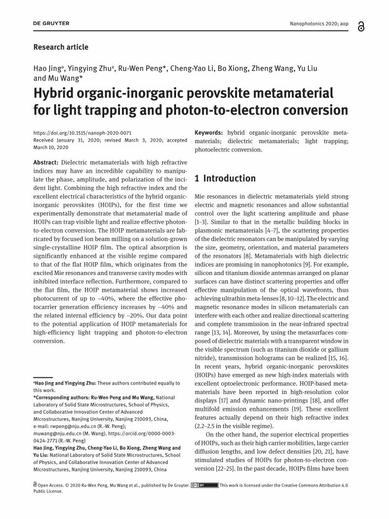
The schematic of the proposed HOIP metamaterial is illustrated in Figure 1A. The metamaterial is made of an array of HOIP nanocubes with identical periods in two orthogonal directions (x and y). The building block of
D
t
p
wd
PerovskiteITO/Glass
xy
z
A B C
0
10
20
30
Wavelength (nm)
Ref
lect
ion
(%)
Tra
nsm
issi
on (
%)
Abs
orpt
ion
(%)
FilmMetamaterial
0
20
40
60
FilmMetamaterial
20
40
60
80
100FilmMetamaterial
M1M2
M3
M4
M5 M6
M7
D1
D2 D3
D4P1
P2 P3P4
400 500 600 700 800
Wavelength (nm)
400 500 600 700 800
Wavelength (nm)
400 500 600 700 800
Figure 1: HOIP metamaterial and its simulated optical properties.(A) Schematic of the HOIP metamaterial. (B–D) Simulated reflection (B), transmission (C), and absorption (D) spectra of the HOIP metamaterial compared to the corresponding spectra from the flat HOIP film. Here, for the HOIP metamaterial t = 300 nm, p = 400 nm, d = 100 nm, and w = 260 nm, while the flat HOIP film has a thickness of 400 nm.

H. Jing et al.: HOIP metamaterial for light trapping and photon-to-electron conversion 3
our metamaterial is designed as an HOIP nanocube on top of the HOIP film on an indium tin oxide (ITO)/glass substrate. The width w and height d of the nanocube are 260 and 100 nm, respectively. The period p of the array is 400 nm. The thicknesses of the HOIP film (t) and the ITO layer are 300 and 180 nm, respectively. Here we employ CH3NH3PbBr3 (MAPbBr3) as a typical HOIP material to construct the nanocubes and the film. Fur-thermore, a control sample of flat MAPbBr3 film is used with a thickness of 400 nm.
The FDTD method (Lumerical, FDTD Solutions) was used to calculate the reflection and the transmission of the structures. In the simulation, periodic boundary con-ditions in the x- and y-directions and perfectly-matched-layer (PML) boundary conditions in the z-direction were applied. The plane-wave source with wavelength in the range 400–800 nm was placed at 2 μm away from the structure. Owing to the fact that the width (w) and period (p) are symmetric in the x-axis and y-axis, the metamate-rial is equivalent for both transverse magnetic (TM)- and transverse electric (TE)-polarized electromagnetic waves for normal incident light. Here, the incident light is nor-mally incident with its polarization along the x-direction.
Figure 1B illustrates the simulated reflection spectra in the wavelength range 400–800 nm. We first examine the reflection spectrum of the flat film (black curve in Figure 1B). A reflection of approximately 15% is obtained for wavelengths <550 nm (i.e. the bandgap energy of MAPbBr3 [43]), and then an oscillatory pattern appears at wavelengths >550 nm. The 15% reflection can be attrib-uted to the reflection at the interface between air and the MAPbBr3 film according to the Fresnel formula. Addition-ally, the two peaks (λ = 559 and 707 nm) in the oscillatory pattern satisfy the constructive interference conditions (phase difference δ = 2mπ, where m is an integer) between the incident and reflected light inside the film. This implies that the Fabry-Perot (F-P) cavity modes appear along the longitudinal direction of the flat MAPbBr3 film. In contrast, for the reflection spectrum of the metamate-rial (red curve in Figure 1B), the reflection drops to nearly zero at wavelengths <550 nm. This indicates that the inter-face reflection is almost inhibited in the metamaterial. Additionally, seven resonance peaks at around 422, 533, 593, 604, 664, 683, and 779 nm appear in the spectrum, which are marked as M1–M7 in Figure 1B. These peaks are related to the various modes excited in the metamaterial and are discussed in the following section.
Figure 1C shows the transmission spectra of the meta-material and the flat film. For the flat film (black curve in Figure 1C), the transmission decreases abruptly at wave-lengths shorter than 550 nm. This is attributed to the
absorption of the MAPbBr3 material. Moreover, two dips appear: one at 526 nm, which corresponds to the absorp-tion by excitons in MAPbBr3 [44], and another broad dip at 707 nm, which arises from the F-P cavity mode, as discussed previously. In contrast, for the metamaterial (red curve in Figure 1C), with the exception of exciton absorption, four dips appear at 604, 664, 680, and 779 nm (respectively marked as D1–D4 in Figure 1C). The locations of these four transmission dips precisely match the peaks M4–M7 in the reflection spectrum. This suggests that they also originate from the various resonance modes like the peaks in the reflection spectrum.
Based on the reflection and transmission data, the absorption (A) in the structure can be calculated from the relationship A = 1 – R –T , where R and T are the reflec-tion and transmission, respectively. Figure 1D illustrates the absorption spectra of the flat film and the metamate-rial. We can see that the absorption of the metamaterial (red curve in Figure 1D) is obviously enhanced compared to that of the flat film (black curve in Figure 1D) and has values above 87% in the spectral range 400–535 nm. This enhancement can be attributed to the inhibition of the interface reflection in the metamaterial, which has been demonstrated in the reflection spectrum. Furthermore, four absorption peaks are observed around 604, 664, 680, and 779 nm (marked as P1–P4 in Figure 1D), where P1 matches M4 in the reflection spectrum and D1 in the transmission spectrum, P2 matches M5 and D2, and the rest may be deduced by analogy. These peaks indicate that the metamaterial can enhance absorption in some spec-tral ranges, specifically at wavelengths >550 nm.
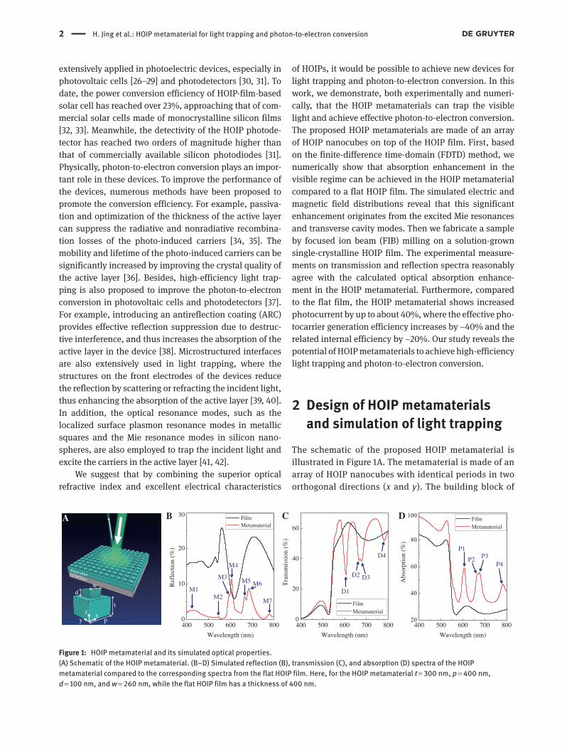
To clarify the resonance modes corresponding to the peaks in the reflection spectrum (and the dips in the trans-mission and the peaks in the absorption spectra), the elec-tric field and magnetic field distributions are monitored, including the vertical sections (xz- or yz-planes) at the center of the nanocube and the transverse section (xy-plane) at the bottom of the nanocube. It is observed that four characteristic modes exist in this system at different wavelengths. The first mode appears at the wavelength of 422 nm (i.e. M1 in the reflection spectrum), as shown in Figure 2A, where a confined electric resonance mode can be observed in the nanocube. This mode can be distin-guished as an electric dipole mode along the x-direction from the cross-section of the normalized electric field distribution shown in Figure 2B. When the wavelength of the incident light gradually increases, the electric dipole mode fades away, and a magnetic resonance mode gradu-ally appears and becomes most obvious at the wavelength 533 nm (i.e. M2 in the reflection spectrum), as illustrated in Figure 2C. Based on the cross-section of the magnetic
4 H. Jing et al.: HOIP metamaterial for light trapping and photon-to-electron conversion
field distribution shown in Figure 2D, this resonance mode exhibits the feature of a magnetic dipole mode along the y-direction.
As the wavelength increases continuously, the energy of the incident photons becomes smaller than the bandgap of the MAPbBr3 (i.e. λ > 550 nm). This means that the MAPbBr3 film will hardly absorb any photon. At this condition, light can completely propagate through the MAPbBr3 film and be reflected by the bottom interface, as shown in the electric field distribution in the flat film of Figure 2E. Accordingly, the reflected light can interfere with the incident light and can induce the F-P resonance modes observed in the reflection and transmission spectra as mentioned above. However, the F-P resonance modes disappear in the metamaterial. Instead, two types of trans-verse cavity modes appear. One is the transverse cavity mode mainly confined between adjacent nanotubes, as shown in Figure 2E and F at the wavelength 593 nm (i.e. M3 in the reflection spectrum). The other is the high-index transverse cavity mode at the wavelength 604 nm (i.e. M4 in the reflection spectrum), which is not excited in the spatial region between the surrounding nanocubes but inside the period of the building block [45], as illustrated in Figure 2G. Compared to the transverse cavity mode at 593 nm, this mode exhibits a stronger electric field con-fined in the MAPbBr3 layer, which corresponds to the
electric field distribution shown in Figure 2H. These two transverse cavity modes will appear again when the wave-length increases, and will include the modes between adjacent nanocubes that appear as M5 (λ = 664 nm) and M7 (λ = 779 nm) and the modes inside the own periods that appear as M6 (λ = 683 nm). Based on the electric/magnetic field distributions, we can conclude that the incident light efficiently excites the Mie resonance modes and transverse cavity modes inside the MAPbBr3 metama-terial instead of being reflected directly at the interface of the flat film. Meanwhile, the F-P resonance modes are also inhibited. The conversion from the incident light to the multiple resonance modes significantly traps the light inside the MAPbBr3 metamaterial and thus enhances the absorption of the metamaterial compared to the flat film.
In the cases of the electric and magnetic resonances, the modes are dependent of both the height and diameter of the dielectric resonator, which are analytically esti-mated by utilizing of the magnetic wall boundary condi-tions [46]. The absorption can be tuned by varying the resonance modes in the metamaterial by using different building blocks (including different heights and widths). Hence, a strong absorption can be achieved by optimiz-ing the structural geometry of the nanocubes. As shown in Figure 3A and B, the absorption of the metamaterial are obtained at different widths (w) and heights (d) as a
2
1
0
0
1
200
0
800
150
–150
2
1
0
–1
1
0
0
800
150
–150
Film Cube Film Cube
0
800 2
1
0
0
1150
–150
A
B
C
D
E
F
0
800
–200 –200200
2
1
0Film Cube Film Cube
0
1150
–150
G
H
λ = 422 nm λ = 533 nm λ = 593 nm λ = 604 nmz
(nm
)y
(nm
)
x (n
m)
x (n
m)
y (n
m)
x (nm)
–200 200x (nm)
–200 200y (nm)
–200 200y (nm)
–200 200x (nm)
200–200 –200200y (nm)
200–200 –200200x (nm)
200–200 –200200x (nm)
z (n
m)
z (n
m)
z (n
m)
|H|
|E|
|E|
|E|
|Ex|
|Ex|
|Ex|
Re
(Hy)
Figure 2: Electric and magnetic field distributions of four different modes.(A) Electric field distributions of the flat film (left panel) and metamaterial (right panel) at the xz-plane with an excitation wavelength of 422 nm. (B) Corresponding electric field distribution of the metamaterial at the xy-plane at the bottom of the nanocube (z = 300 nm). (C) Magnetic field distributions of the flat film (left panel) and metamaterial (right panel) in the yz-plane with an excitation wavelength of 533 nm. (D) Corresponding magnetic field distribution of the metamaterial at the yx-plane at the bottom of the nanocube. (E–H) Electric field distributions of the flat film (left panel) and metamaterial (right panel) in the xz-plane with the excitation wavelength of 593 nm (E) and 604 nm (G) and the corresponding electric field distributions of the metamaterial at the xy-plane at the bottom of the nanocube at 593 nm (F) and 604 nm (H). Here the HOIP metamaterial has the following structural parameters: t = 300 nm, p = 400 nm, d = 100 nm, and w = 260 nm, while the flat HOIP film has a thickness of 400 nm.
H. Jing et al.: HOIP metamaterial for light trapping and photon-to-electron conversion 5
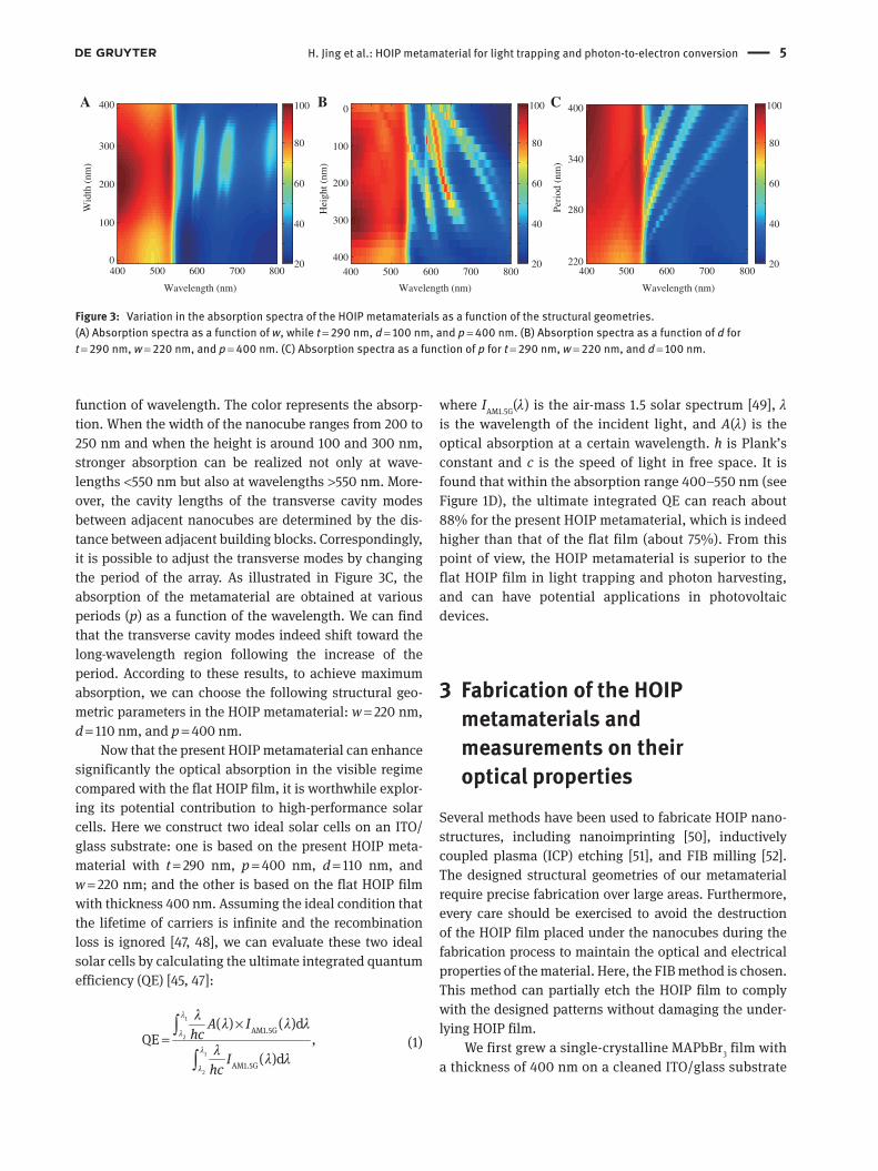
function of wavelength. The color represents the absorp-tion. When the width of the nanocube ranges from 200 to 250 nm and when the height is around 100 and 300 nm, stronger absorption can be realized not only at wave-lengths <550 nm but also at wavelengths >550 nm. More-over, the cavity lengths of the transverse cavity modes between adjacent nanocubes are determined by the dis-tance between adjacent building blocks. Correspondingly, it is possible to adjust the transverse modes by changing the period of the array. As illustrated in Figure 3C, the absorption of the metamaterial are obtained at various periods (p) as a function of the wavelength. We can find that the transverse cavity modes indeed shift toward the long-wavelength region following the increase of the period. According to these results, to achieve maximum absorption, we can choose the following structural geo-metric parameters in the HOIP metamaterial: w = 220 nm, d = 110 nm, and p = 400 nm.
Now that the present HOIP metamaterial can enhance significantly the optical absorption in the visible regime compared with the flat HOIP film, it is worthwhile explor-ing its potential contribution to high-performance solar cells. Here we construct two ideal solar cells on an ITO/glass substrate: one is based on the present HOIP meta-material with t = 290 nm, p = 400 nm, d = 110 nm, and w = 220 nm; and the other is based on the flat HOIP film with thickness 400 nm. Assuming the ideal condition that the lifetime of carriers is infinite and the recombination loss is ignored [47, 48], we can evaluate these two ideal solar cells by calculating the ultimate integrated quantum efficiency (QE) [45, 47]:
1
2
1
2
AM1.5G
AM1.5G
( ) ( )dQE ,
( )d
A Ihc
Ihc
λ
λ
λ
λ
λλ λ λ
λλ λ
×=
∫
∫ (1)
where IAM1.5G(λ) is the air-mass 1.5 solar spectrum [49], λ is the wavelength of the incident light, and A(λ) is the optical absorption at a certain wavelength. h is Plank’s constant and c is the speed of light in free space. It is found that within the absorption range 400–550 nm (see Figure 1D), the ultimate integrated QE can reach about 88% for the present HOIP metamaterial, which is indeed higher than that of the flat film (about 75%). From this point of view, the HOIP metamaterial is superior to the flat HOIP film in light trapping and photon harvesting, and can have potential applications in photovoltaic devices.
3 Fabrication of the HOIP metamaterials and measurements on their optical properties
Several methods have been used to fabricate HOIP nano-structures, including nanoimprinting [50], inductively coupled plasma (ICP) etching [51], and FIB milling [52]. The designed structural geometries of our metamaterial require precise fabrication over large areas. Furthermore, every care should be exercised to avoid the destruction of the HOIP film placed under the nanocubes during the fabrication process to maintain the optical and electrical properties of the material. Here, the FIB method is chosen. This method can partially etch the HOIP film to comply with the designed patterns without damaging the under-lying HOIP film.
We first grew a single-crystalline MAPbBr3 film with a thickness of 400 nm on a cleaned ITO/glass substrate
400 500 600 700 8000
100
200
Wid
th (
nm)
Hei
ght (
nm)
Peri
od (
nm)
300
400
20
40
60
80
100A
400 500 600 700 800
0
100
200
300
40020
40
60
80
100B
400 500 600 700 800220
280
340
400C
20
40
60
80
100
Wavelength (nm) Wavelength (nm) Wavelength (nm)
Figure 3: Variation in the absorption spectra of the HOIP metamaterials as a function of the structural geometries.(A) Absorption spectra as a function of w, while t = 290 nm, d = 100 nm, and p = 400 nm. (B) Absorption spectra as a function of d for t = 290 nm, w = 220 nm, and p = 400 nm. (C) Absorption spectra as a function of p for t = 290 nm, w = 220 nm, and d = 100 nm.

6 H. Jing et al.: HOIP metamaterial for light trapping and photon-to-electron conversion
with the use of the solution process as reported previ-ously [53]. Then we fabricated the designed metamaterial by etching the MAPbBr3 film for 180 s using a dual-beam FIB system (Helios, Nanolab 600i) under an operating current of 20 pA and operating voltage of 30 kV. Figure 4A shows the scanning electron microscopy (SEM) images of the MAPbBr3 metamaterial, wherein uniform nanocubes are arranged in neat rows within an area of 20 μm2. The details are shown in the inset, where square cubes with widths 223 nm and periods 402 nm can be observed, which match well the designed parameters. A titled SEM image of the metamaterial is shown in Figure 4B, wherein the etching depth is about 120 nm. Figure 4C shows the reflection image of a flat MAPbBr3 film with the metamaterial in the middle. A striking color con-trast can be observed between the untreated film and the metamaterial. The dark black color of the middle region demonstrates an obvious decrease in the reflec-tion response.
Figure 5A–C illustrates the reflection, transmission, and absorption spectra of the metamaterial and the flat film measured using an ultraviolet-visible-near-infrared (UV-vis-NIR) microspectrophotometer (CRAIC, QDI2010). As shown, for the flat film (black curve in Figure 5A), the reflection is approximately 17% at wavelengths <550 nm, and an oscillatory pattern is observed with peaks at 559 and 707 nm. In contrast, the reflection spectrum of the metamaterial (red curve in Figure 5A) shows an obvious decrease in reflection compared to that of the flat film and approaches zero in the wavelength range 400–550 nm. Additionally, five peaks can be observed at 538, 612, 630, 709, and 730 nm (respectively marked as M′1–M′5 in Figure 5A). These results are similar to the simu-lated results, even though the transverse cavity modes (M′2–M′5) are all red-shifted and broadened compared to
the simulation results (M3–M7), which may be attributed to the adjustment of the structural geometries and the deviation generated during the milling process. Figure 5B shows the transmission spectra of the flat film (black curve) and the metamaterial (red curve). Similar to the reflection spectra, the dips from the transverse cavity modes are also broadened and emerge as continuous dips in the transmission spectrum in the wavelength range 530–680 nm.
Figure 5C shows the absorption spectra of the flat film (black curve) and the metamaterial (red curve). The absorption in the range 400–530 nm increases by 7–15% compared to that of the flat film. For wavelengths >530 nm, the increase in absorption is much more obvious owing to the decrease in transmission shown in Figure 5B. In addition, the absorption of the meta-material is even higher by 53% compared to that of the flat film at 560 nm. These results demonstrate that the MAPbBr3 metamaterial has obvious absorption enhance-ment compared to the flat MAPbBr3 film in the visible range.
To present the insensitivity to polarization of the metamaterial in absorption enhancement, we have meas-ured the absorption spectra of the metamaterial and the flat film under linearly polarized light at various polari-zations (0° means polarization along the x-direction). We defined the absorption enhancement factor as the ratio between the integrated areas of the absorption spectra of the metamaterial and the flat film. Here, two wavelength ranges were studied: the absorbable range (400–550 nm), and the entire visible range (400–800 nm). We can see in Figure 5D that, irrespective of the wavelength range, the absorption enhancement factors are almost unchanged at various polarization angles. This is attributed to the “isotropy” of the metamaterial.
500 nm x
y
B CA
5 µm10 µm
Figure 4: Scanning electron microscopy (SEM) and reflection images of the fabricated metamaterial.(A) SEM images of the metamaterial (scale bar: 5 μm). Inset: SEM image of the enlarged area. (B) Tilted SEM image at the tilt angle of 52°. (C) Reflection image of a MAPbBr3 film. Decreased reflection is observed in the middle part where the metamaterial is located.

H. Jing et al.: HOIP metamaterial for light trapping and photon-to-electron conversion 7
4 Experimental measurements of the electrical characteristics of HOIP metamaterials
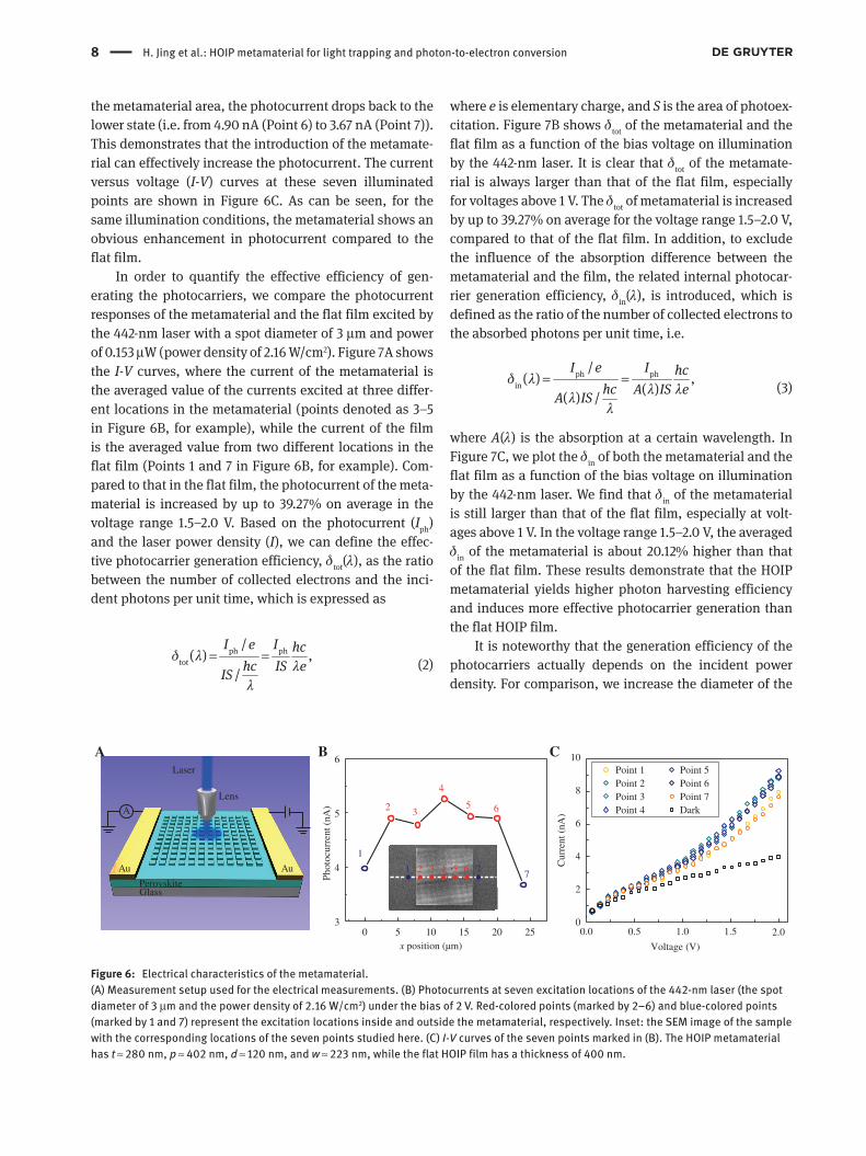
Owing to the fact that the photo-induced carriers in the sample can be collected at the bias voltage, electrical measurements were carried out to explore the effective efficiency of generating photocarriers. Here we try to compare the photocurrents of the metamaterial and the flat film under the same illumination. The schematic of the measurement setup is shown in Figure 6A. A single-crystalline MAPbBr3 film with a thickness of 400 nm was grown on a cleaned glass substrate using a solu-tion process as before. Then, a pair of gold electrodes (50 nm in thickness) was deposited on both sides of the metamaterial using electron-gun evaporation. After that, we fabricated the metamaterial by using a dual-beam FIB system under the same conditions as described in Section 3 (i.e. operating current = 20 pA, operating voltage = 30 kV, and milling time = 180 s). A source meter (Keithley Instruments, 2636B) was used to apply bias volt-ages and to detect the current signals simultaneously. A
laser (CNIlaser, MDL-III-442) operating at a wavelength of 442 nm and with a stable power of 0.153 μW was focused on the sample to generate the carriers.
We first study how the metamaterial influences the electrical characteristics. Photocurrents (Ip, Ip = I – Idark, where Idark is the dark current) were measured when the sample was illuminated by the laser (with a laser spot dia-meter of 3 μm) at seven discrete points (successive points separated by 4 μm), as shown in the inset of Figure 6B. Here the first and the last illuminated points are outside the metamaterial (shown in blue, i.e. Points 1 and 7), whereas the other five illuminated points are inside the metamaterial (shown in red, i.e. Points 2–6). It is worth mentioning that the seven points are aligned parallel to the electrodes (white dashed line in the inset of Figure 6B), which reduces the influence of carrier diffusion [54]. For a bias voltage of 2 V, as depicted in Figure 6B, we can see an obvious increase in the photocurrent from 3.98 to 4.90 nA when the laser spot moves from the flat film to the metamaterial region (i.e. from Point 1 to Point 2). Further, a higher photocurrent state (at approximately 5 nA) is maintained when the laser spot is on the metamaterial (Points 2 to 6). Finally, when the laser spot moves outside
A
400 500 600 700 800
0
10Ref
lect
ion
(%)
Tra
nsm
issi
on (
%)
20
30
40
Wavelength (nm)
400 500 600 700 800
Wavelength (nm)
400 500 600 700 800
Wavelength (nm)
FilmMetamaterial
0
20
40
60
80
Abs
orpt
ion
(%)
FilmMetamaterial
0
20
40
60
80
100
FilmMetamaterial
M 1
M 2M 3
M 4
M 5
0
30
6090
120
150
180
210
240270
300
330
0.0
0.5
1.0
1.5
2.0
0.5
1.0
1.5
2.0
Abs
orpt
ion
enha
ncem
ent f
acto
r
400–800 nm400–550 nm
B
C D
Figure 5: Optical properties measured experimentally.(A–C) Measured reflection (A), transmission (B), and absorption (C) spectra of a metamaterial in comparison with those of the flat film. (D) Absorption enhancement factors of the metamaterial at different light polarizations. The red-colored points represent the absorbable wavelength range (400–550 nm), whereas the blue-colored points represent the entire visible range (400–800 nm). Here, the HOIP metamaterial has t ≈ 280 nm, p ≈ 402 nm, d ≈ 120 nm, and w ≈ 223 nm, while the flat HOIP film has the thickness of 400 nm.
8 H. Jing et al.: HOIP metamaterial for light trapping and photon-to-electron conversion
the metamaterial area, the photocurrent drops back to the lower state (i.e. from 4.90 nA (Point 6) to 3.67 nA (Point 7)). This demonstrates that the introduction of the metamate-rial can effectively increase the photocurrent. The current versus voltage (I-V) curves at these seven illuminated points are shown in Figure 6C. As can be seen, for the same illumination conditions, the metamaterial shows an obvious enhancement in photocurrent compared to the flat film.
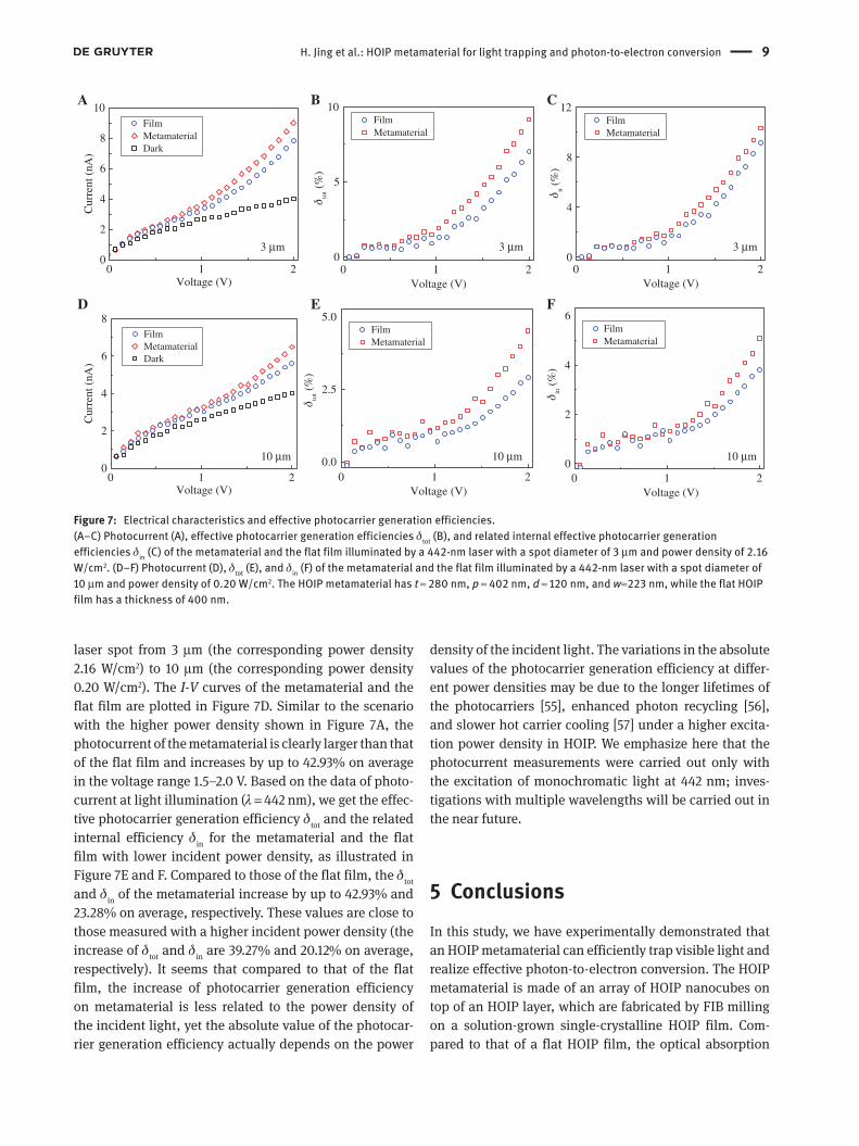
In order to quantify the effective efficiency of gen-erating the photocarriers, we compare the photocurrent responses of the metamaterial and the flat film excited by the 442-nm laser with a spot diameter of 3 μm and power of 0.153 μW (power density of 2.16 W/cm2). Figure 7A shows the I-V curves, where the current of the metamaterial is the averaged value of the currents excited at three differ-ent locations in the metamaterial (points denoted as 3–5 in Figure 6B, for example), while the current of the film is the averaged value from two different locations in the flat film (Points 1 and 7 in Figure 6B, for example). Com-pared to that in the flat film, the photocurrent of the meta-material is increased by up to 39.27% on average in the voltage range 1.5–2.0 V. Based on the photocurrent (Iph) and the laser power density (I), we can define the effec-tive photocarrier generation efficiency, δtot(λ), as the ratio between the number of collected electrons and the inci-dent photons per unit time, which is expressed as
ph phtot
/( ) ,
/
I e I hchc IS eIS
δ λλ
λ
= = (2)
where e is elementary charge, and S is the area of photoex-citation. Figure 7B shows δtot of the metamaterial and the flat film as a function of the bias voltage on illumination by the 442-nm laser. It is clear that δtot of the metamate-rial is always larger than that of the flat film, especially for voltages above 1 V. The δtot of metamaterial is increased by up to 39.27% on average for the voltage range 1.5–2.0 V, compared to that of the flat film. In addition, to exclude the influence of the absorption difference between the metamaterial and the film, the related internal photocar-rier generation efficiency, δin(λ), is introduced, which is defined as the ratio of the number of collected electrons to the absorbed photons per unit time, i.e.
ph phin
/( ) ,
( )( ) /
I e I hchc A IS eA IS
δ λλ λ
λλ
= = (3)
where A(λ) is the absorption at a certain wavelength. In Figure 7C, we plot the δin of both the metamaterial and the flat film as a function of the bias voltage on illumination by the 442-nm laser. We find that δin of the metamaterial is still larger than that of the flat film, especially at volt-ages above 1 V. In the voltage range 1.5–2.0 V, the averaged δin of the metamaterial is about 20.12% higher than that of the flat film. These results demonstrate that the HOIP metamaterial yields higher photon harvesting efficiency and induces more effective photocarrier generation than the flat HOIP film.
It is noteworthy that the generation efficiency of the photocarriers actually depends on the incident power density. For comparison, we increase the diameter of the
A
Lens
Laser
PerovskiteGlass
uAuA 1 72 3 4 5 6
1
2 3
4
5 6
7
A
0
2
4
6
8
10Point 1 Point 5Point 2 Point 6Point 3 Point 7Point 4 Dark
Cur
rent
(nA
)
Voltage (V)
0.0 0.5 1.0 1.5 2.00 5 10 15 20 253
4
5
6
Phot
ocur
rent
(nA
)
x position (µm)
CB
Figure 6: Electrical characteristics of the metamaterial.(A) Measurement setup used for the electrical measurements. (B) Photocurrents at seven excitation locations of the 442-nm laser (the spot diameter of 3 μm and the power density of 2.16 W/cm2) under the bias of 2 V. Red-colored points (marked by 2–6) and blue-colored points (marked by 1 and 7) represent the excitation locations inside and outside the metamaterial, respectively. Inset: the SEM image of the sample with the corresponding locations of the seven points studied here. (C) I-V curves of the seven points marked in (B). The HOIP metamaterial has t ≈ 280 nm, p ≈ 402 nm, d ≈ 120 nm, and w ≈ 223 nm, while the flat HOIP film has a thickness of 400 nm.
H. Jing et al.: HOIP metamaterial for light trapping and photon-to-electron conversion 9
laser spot from 3 μm (the corresponding power density 2.16 W/cm2) to 10 μm (the corresponding power density 0.20 W/cm2). The I-V curves of the metamaterial and the flat film are plotted in Figure 7D. Similar to the scenario with the higher power density shown in Figure 7A, the photocurrent of the metamaterial is clearly larger than that of the flat film and increases by up to 42.93% on average in the voltage range 1.5–2.0 V. Based on the data of photo-current at light illumination (λ = 442 nm), we get the effec-tive photocarrier generation efficiency δtot and the related internal efficiency δin for the metamaterial and the flat film with lower incident power density, as illustrated in Figure 7E and F. Compared to those of the flat film, the δtot and δin of the metamaterial increase by up to 42.93% and 23.28% on average, respectively. These values are close to those measured with a higher incident power density (the increase of δtot and δin are 39.27% and 20.12% on average, respectively). It seems that compared to that of the flat film, the increase of photocarrier generation efficiency on metamaterial is less related to the power density of the incident light, yet the absolute value of the photocar-rier generation efficiency actually depends on the power
density of the incident light. The variations in the absolute values of the photocarrier generation efficiency at differ-ent power densities may be due to the longer lifetimes of the photocarriers [55], enhanced photon recycling [56], and slower hot carrier cooling [57] under a higher excita-tion power density in HOIP. We emphasize here that the photocurrent measurements were carried out only with the excitation of monochromatic light at 442 nm; inves-tigations with multiple wavelengths will be carried out in the near future.
5 ConclusionsIn this study, we have experimentally demonstrated that an HOIP metamaterial can efficiently trap visible light and realize effective photon-to-electron conversion. The HOIP metamaterial is made of an array of HOIP nanocubes on top of an HOIP layer, which are fabricated by FIB milling on a solution-grown single-crystalline HOIP film. Com-pared to that of a flat HOIP film, the optical absorption
B CA
3 µm 3 µm 3 µm0
2
4
6
8
10FilmMetamaterialDark
Cur
rent
(nA
)C
urre
nt (
nA)
Voltage (V)
0
5
10FilmMetamaterial
δ tot (
%)
δ n (%
)
δ tot (
%)
δ in (
%)
Voltage (V)
0
4
8
12FilmMetamaterial
Voltage (V)
0
2
4
6
8FilmMetamaterialDark
Voltage (V)
0.0
2.5
5.0FilmMetamaterial
Voltage (V)
0 1 2 0 1 2 0 1 2
0 1 2 0 1 2 0 1 20
2
4
6FilmMetamaterial
Voltage (V)
D E F
10 µm10 µm10 µm
Figure 7: Electrical characteristics and effective photocarrier generation efficiencies.(A–C) Photocurrent (A), effective photocarrier generation efficiencies δtot (B), and related internal effective photocarrier generation efficiencies δin (C) of the metamaterial and the flat film illuminated by a 442-nm laser with a spot diameter of 3 μm and power density of 2.16 W/cm2. (D–F) Photocurrent (D), δtot (E), and δin (F) of the metamaterial and the flat film illuminated by a 442-nm laser with a spot diameter of 10 μm and power density of 0.20 W/cm2. The HOIP metamaterial has t ≈ 280 nm, p ≈ 402 nm, d ≈ 120 nm, and w≈223 nm, while the flat HOIP film has a thickness of 400 nm.
10 H. Jing et al.: HOIP metamaterial for light trapping and photon-to-electron conversion
of this structure is significantly enhanced owing to the excited Mie resonances, the transverse cavity modes within the HOIP metamaterial, and the inhibition of reflection loss at the interface. Furthermore, photocurrent measurements have shown that the photocurrent of the HOIP metamaterial increases by up to ~40% compared to that of a flat HOIP film. For the photon-to-electron conver-sion, the metamaterial yields ~40% increase in the effec-tive photocarrier generation efficiency and ~20% increase in the related internal efficiency compared to the values of the flat film. Our study reveals the potential of the HOIP dielectric metamaterials to achieve high-efficiency light trapping, extends the applications of dielectric metamate-rials to photon-to-electron conversion, and demonstrates a unique way of achieving novel HOIP-dielectric metama-terial photoelectric nanodevices.
Acknowledgment: This work was supported by the National Key R&D Program of China (2017YFA0303702), and the National Natural Science Foundation of China (Grant Nos. 11634005, 11974177, 61975078, 11674155).
References[1] Kamali SM, Arbabi E, Arbabi A, Faraon A. A review of dielectric
optical metasurfaces for wavefront control. Nanophotonics 2018;7:1041–68.
[2] Zhao Q, Zhou J, Zhang F. Lippens D. Mie resonance-based dielectric metamaterials. Mater Today 2009;12:60–9.
[3] Jahani S, Jacob Z. All-dielectric metamaterials. Nat Nanotechnol 2016;11:23–36.
[4] Jiang SC, Xiong X, Hu YS, et al. High-efficiency generation of circularly polarized light via symmetry-induced anomalous reflection. Phys Rev B 2015;91:125421.
[5] Sun S, He Q, Xiao S, Xu Q, Zhou L. Gradient-index meta-surfaces as a bridge linking propagating waves and surface waves. Nat Mater 2012;11:426–31.
[6] Huang L, Chen X, Mühlenbernd H, et al. Three-dimensional optical holography using a plasmonic metasurface. Nat Com-mun 2013;4:2808.
[7] Ma W, Cheng F, Liu Y. Deep-learning-enabled on-demand design of chiral metamaterials. ACS Nano 2018;12:6326–34.
[8] Lin D, Fan P, Hasman E, Brongersma ML. Dielectric gradient metasurface optical elements. Science 2014;345:298–302.
[9] Kuznetsov AI, Miroshnichenko AE, Brongersma ML, Kivshar YS, Luk’yanchuk B. Optically resonant dielectric nanostructures. Science 2016;354:aag2472.
[10] Aieta F, Kats MA, Genevet P, Capasso F. Multiwavelength achromatic metasurfaces by dispersive phase compensation. Science 2015;347:1342–5.
[11] Khorasaninejad M, Chen WT, Devlin RC, Oh J, Zhu AY, Capasso F. Metalenses at visible wavelengths: diffraction-limited focusing and subwavelength resolution imaging. Science 2016;352:1190–4.
[12] Wang S, Wu PC, Su VC, et al. A broadband achromatic metalens in the visible. Nat Nanotechnol 2018;13:227–32.
[13] Staude I, Miroshnichenko AE, Decker M, et al. Tailor-ing directional scattering through magnetic and electric resonances in subwavelength silicon nanodisks. ACS Nano 2013;7:7824–32.
[14] Yang Y, Kravchenko II, Briggs DP, Valentine J. All-dielectric metasurface analogue of electromagnetically induced transpar-ency. Nat Commun 2014;5:5753.
[15] Ren H, Briere G, Fang X, et al. Metasurface orbital angular momentum holography. Nat Commun 2019;10:2986.
[16] Devlin RC, Khorasaninejad M, Chen WT, Oh J, Capasso F. Broad-band high-efficiency dielectric metasurfaces for the visible spectrum. PNAS 2016;113:10473–8.
[17] Gholipour B, Adamo G, Cortecchia D, et al. Organometallic perovskite metasurfaces. Adv Mater 2017;29:1604268.
[18] Gao Y, Huang C, Hao C, et al. Lead halide perovskite nanostruc-tures for dynamic color display. ACS Nano 2018;12:8847–54.
[19] Makarov SV, Milichko V, Ushakova EV, et al. Multifold emission enhancement in nanoimprinted hybrid perovskite metasur-faces. ACS Photon 2017;4:728–35.
[20] Stranks SD, Eperon GE, Grancini G, et al. Electron-hole diffusion lengths exceeding 1 micrometer in an organometal trihalide perovskite absorber. Science 2013;342:341–4.
[21] Green MA, Ho-Baillie A, Snaith HJ. The emergence of perovskite solar cells. Nat Photon 2014;8:506–14.
[22] Liu M, Johnston MB, Snaith HJ. Efficient planar heterojunc-tion perovskite solar cells by vapor deposition. Nature 2013;501:395–8.
[23] Tan ZK, Moghaddam RS, Lai ML, et al. Bright light-emitting diodes based on organometal halide perovskite. Nat Nanotech-nol 2014;9:687–92.
[24] Lin K, Xing J, Quan LN, et al. Perovskite light-emitting diodes with external quantum efficiency exceeding 20 percent. Nature 2018;562:245–8.
[25] Sahli F, Werner J, Kamino BA, et al. Fully textured monolithic perovskite/silicon tandem solar cells with 25.2% power conversion efficiency. Nat Mater 2018;17:820–6.
[26] Zhou H, Chen Q, Li G, et al. Interface engineering of highly efficient perovskite solar cells. Science 2014;345:542–6.
[27] Burschka J, Pellet N, Moon SJ, et al. Sequential deposition as a route to high-performance perovskite-sensitized solar cells. Nature 2013;499:316–9.
[28] Yang WS, Noh JH, Jeon NJ, et al. High-performance photovoltaic perovskite layers fabricated through intramolecular exchange. Science 2015;348:1234–7.
[29] Congreve DN, Lee J, Thompson NJ, et al. External quantum effi-ciency above 100% in a singlet-exciton-fission-based organic photovoltaic cell. Science 2013;340:334–7.
[30] Xie C, You P, Liu Z, Li L, Yan F. Ultrasensitive broadband phototransistors based on perovskite/organic-semiconductor vertical heterojunctions. Light Sci Appl 2017;6:e17023.
[31] Feng J, Gong C, Gao H, et al. Single-crystalline layered metal-halide perovskite nanowires for ultrasensitive photodetectors. Nat Electron 2018;1:404–10.
[32] Jiang Q, Zhao Y, Zhang X, et al. Surface passivation of perovs-kite film for efficient solar cells. Nat Photon 2019;13:460–6.
[33] Meng L, You J, Yang Y. Addressing the stability issue of per-ovskite solar cells for commercial applications. Nat Commun 2018;9:5265.
H. Jing et al.: HOIP metamaterial for light trapping and photon-to-electron conversion 11
[34] Chen B, Rudd PN, Yang S, Yuan Y, Huang J. Imperfections and their passivation in halide perovskite solar cells. Chem Soc Rev 2019;48:3842–67.
[35] Yang Z, Deng Y, Zhang X, et al. High-performance single-crystalline perovskite thin-film photodetector. Adv Mater 2018;30:1704333.
[36] Saidaminov MI, Abdelhady AL, Murali B, et al. High-quality bulk hybrid perovskite single crystals within minutes by inverse temperature crystallization. Nat Commun 2015;6:7586.
[37] Brongersma ML, Cui Y, Fan S. Light management for photovolta-ics using high-index nanostructures. Nat Mater 2014;13:451–60.
[38] Zhao J, Green MA. Optimized antireflection coatings for high-effi-ciency silicon solar cells. IEEE T Electron Dev 1991;38:1925–34.
[39] Jošt M, Albrecht S, Kegelmann L, et al. Efficient light manage-ment by textured nanoimprinted layers for perovskite solar cells. ACS Photon 2017;4:1232–9.
[40] Wei J, Xu RP, Li YQ, et al. Enhanced light harvesting in perovs-kite solar cells by a bioinspired nanostructured back electrode. Adv Energy Mater 2017;7:1700492.
[41] Du B, Yang W, Jiang Q, et al. Plasmonic-functionalized broad-band perovskite photodetector. Adv Opt Mater 2018;6:1701271.
[42] Tiguntseva E, Chebykin A, Ishteev A, et al. Resonant silicon nanoparticles for enhancement of light absorption and photo-luminescence from hybrid perovskite films and metasurfaces. Nanoscale 2017;9:12486–93.
[43] Wu B, Nguyen HT, Ku Z, et al. Discerning the surface and bulk recombination kinetics of organic-inorganic halide perovskite single crystals. Adv Energy Mater 2016;6:1600551.
[44] Yang Y, Yan Y, Yang M, et al. Low surface recombination velocity in solution-grown CH3NH3PbBr3 perovskite single crystal. Nat Commun 2015;6:7961.
[45] Zhu LH, Shao MR, Peng RW, Fan RH, Huang XR, Wang M. Broadband absorption and efficiency enhancement of an ultra-thin silicon solar cell with a plasmonic fractal. Opt Express 2013;21:A313–23.
[46] Long SA, McAllister MW, Shen LC. The resonant cylindri-cal dielectric cavity antenna. IEEE Trans Antennas Propag 1983;31:406–12.
[47] Shockley W, Queisser HJ. Detailed balance limit of efficiency of p-n junction solar cells. J Appl Phys 1961;32:510.
[48] Peng RW, Mazzer M, Barnham KWJ. Efficiency enhancement of ideal photovoltaic solar cells by photonic excitations in multi-intermediate band structures. Appl Phys Lett 2003;83:770–2.
[49] ASTM. Reference solar spectral irradiance: air mass 1.5 spec-tra. Available at: http://rredc.nrel.gov/solar/spectra/am1.5. Accessed: 24 February 2020.
[50] Wang H, Haroldson R, Balachandran B, et al. Nanoimprinted perovskite nanograting photodetector with improved effi-ciency. ACS Nano 2016;10:10921–8.
[51] Zhang C, Xiao S, Wang Y, et al. Lead halide perovskite-based dynamic metasurfaces. Laser Photon Rev 2019;13:1900079.
[52] Alias MS, Yang Y, Ng TK, et al. Enhanced etching, surface dam-age recovery, and submicron patterning of hybrid perovs-kites using a chemically gas-assisted focused-ion beam for subwavelength grating photonic applications. J Phys Chem Lett 2016;7:137–42.
[53] Wang D, Shi WB, Jing H, et al. Photon-induced carrier recombi-nation in the nonlayered-structured hybrid organic-inorganic perovskite nano-sheets. Opt Express 2018;26:27504–14.
[54] Liu S, Wang L, Lin WC, Sucharitakul S, Burda C, Gao XP. Imag-ing the long transport lengths of photo-generated carriers in oriented perovskite films. Nano Lett 2016;16:7925–9.
[55] Zheng K, Žídek K, Abdellah M, Messing ME, Al-Marri MJ, Pullerits T. Trap states and their dynamics in organometal halide perovskite nanoparticles and bulk crystals. J Phys Chem C 2016;120:3077–84.
[56] Pazos-Outón LM, Szumilo M, Lamboll R, et al. Photon recycling in lead iodide perovskite solar cells. Science 2016;351:1430–3.
[57] Fu J, Xu Q, Han G, et al. Hot carrier cooling mechanisms in halide perovskites. Nat Commun 2017;8:1300.