Hybrid light-emitting polymer/SiN x platform for photonic ... · Hybrid light-emitting polymer/SiNx...
8
Fan, Z., Wu, Z., Chen, Y., Shao, Z., Zhang, Y., Qiu, Z., & Yu, S. (2017). Hybrid light-emitting polymer/SiN x platform for photonic integration. Optics Express, 25(26), 33527-33533. https://doi.org/10.1364/OE.25.033527 Publisher's PDF, also known as Version of record Link to published version (if available): 10.1364/OE.25.033527 Link to publication record in Explore Bristol Research PDF-document This is the final published version of the article (version of record). It first appeared online via OSA at https://doi.org/10.1364/OE.25.033527 . Please refer to any applicable terms of use of the publisher. University of Bristol - Explore Bristol Research General rights This document is made available in accordance with publisher policies. Please cite only the published version using the reference above. Full terms of use are available: http://www.bristol.ac.uk/pure/about/ebr-terms
Transcript of Hybrid light-emitting polymer/SiN x platform for photonic ... · Hybrid light-emitting polymer/SiNx...

Fan, Z., Wu, Z., Chen, Y., Shao, Z., Zhang, Y., Qiu, Z., & Yu, S. (2017).Hybrid light-emitting polymer/SiNx platform for photonic integration. OpticsExpress, 25(26), 33527-33533. https://doi.org/10.1364/OE.25.033527
Publisher's PDF, also known as Version of record
Link to published version (if available):10.1364/OE.25.033527
Link to publication record in Explore Bristol ResearchPDF-document
This is the final published version of the article (version of record). It first appeared online via OSA athttps://doi.org/10.1364/OE.25.033527 . Please refer to any applicable terms of use of the publisher.
University of Bristol - Explore Bristol ResearchGeneral rights
This document is made available in accordance with publisher policies. Please cite only the publishedversion using the reference above. Full terms of use are available:http://www.bristol.ac.uk/pure/about/ebr-terms

Hybrid light-emitting polymer/SiNx platform for photonic integration ZEMING FAN,1 ZERU WU,1 YUJIE CHEN,1,3 ZENGKAI SHAO,1 YANFENG ZHANG,1 ZHIREN QIU,1,4 AND SIYUAN YU1,2 1State Key Laboratory of Optoelectronic Materials and Technologies, School of Physics, School of Electronics and Information Technology, Sun Yat-sen University, Guangzhou 510275, China 2Photonics Group, Merchant Venturers School of Engineering, University of Bristol, Bristol BS8 1UB, UK [email protected] [email protected]
Abstract: Organic semiconductors have potentials for a broad range of applications. However, they are difficult to be integrated with traditional inorganic material to meet the need of further applications. Based on low-temperature silicon nitride (SiNx) deposition technique, here we demonstrate a hybrid structure fabricated by directly depositing high-quality SiNx on organic polymer film Poly[2-(2',5′-bis(2”-ethylhexyloxy)- phenyl) −1,4-phenylene vinylene] (BEHP-PPV). Stacked BEHP-PPV/SiNx hybrid structures with different periods are obtained and their optical properties are systematically characterized. Moreover, a group of BEHP-PPV embedded SiNx micro-disks are fabricated and amplification of spontaneous emission (ASE) is observed under optical pumping, further confirming that BEHP-PPV remains stable after the whole fabrication process. Our technique offers a platform to fabricate organic/inorganic hybrid optical devices compatible with integrated components. © 2017 Optical Society of America under the terms of the OSA Open Access Publishing Agreement
OCIS codes: (130.3130) Integrated optics materials; (160.4890) Organic materials; (300.2140) Emission.
References and links 1. R. H. Friend, R. W. Gymer, A. B. Holmes, J. H. Burroughes, R. N. Marks, C. Taliani, D. D. C. Bradley, D. A.
Dos Santos, J. L. Bredas, M. Logdlund, and W. R. Salaneck, “Electroluminescence in conjugated polymers,” Nat. 397(6715), 121–128 (1999).
2. N. Thejo Kalyani and S. J. Dhoble, “Organic light emitting diodes: Energy saving lighting technology—A review,” Renew. Sustain. Energy Rev. 16(5), 2696–2723 (2012).
3. R. Capelli, S. Toffanin, G. Generali, H. Usta, A. Facchetti, and M. Muccini, “Organic light-emitting transistors with an efficiency that outperforms the equivalent light-emitting diodes,” Nat. Mater. 9(6), 496–503 (2010).
4. H. C. Yeh and M. C. Hsieh, “Tuning the emission color of organic semiconductor films with cholesteric liquid crystals,” Opt. Express 25(10), 11211–11216 (2017).
5. Y. Chen, J. Herrnsdorf, B. Guilhabert, A. L. Kanibolotsky, A. R. Mackintosh, Y. Wang, R. A. Pethrick, E. Gu,G. A. Turnbull, and P. J. Skabara, “Laser action in a surface-structured free-standing membrane based on a π-conjugated polymer-composite,” Org. Electron. 12(1), 62–69 (2011).
6. C. Foucher, B. Guilhabert, A. L. Kanibolotsky, P. J. Skabara, N. Laurand, and M. D. Dawson, “RGB and white-emitting organic lasers on flexible glass,” Opt. Express 24(3), 2273–2280 (2016).
7. Y. Wang, X. Yang, H. Li, and C. Sheng, “Bright single-mode random laser from a concentrated solution of π-conjugated polymers,” Opt. Lett. 41(2), 269–272 (2016).
8. M. Mantoku, M. Ichida, I. Umezu, A. Sugimura, and T. Aoki-Matsumoto, “Lasing in organic mixed-crystal thinfilms with cavities composed of naturally formed cracks,” Opt. Lett. 42(8), 1528–1531 (2017).
9. T. Zhai, F. Tong, Y. Wang, X. Wu, S. Li, M. Wang, and X. Zhang, “Polymer lasers assembled by suspendingmembranes on a distributed feedback grating,” Opt. Express 24(19), 22028–22033 (2016).
10. D. T. McQuade, A. E. Pullen, and T. M. Swager, “Conjugated polymer-based chemical sensors,” Chem. Rev. 100(7), 2537–2574 (2000).
11. J. Clark and G. Lanzani, “Organic photonics for communications,” Nat. Photonics 4(7), 438–446 (2010). 12. Y. Enami, C. T. Derose, D. Mathine, C. Loychik, C. Greenlee, R. A. Norwood, T. D. Kim, J. Luo, Y. Tian, A.
K. Y. Jen, and N. Peyghambarian, “Hybrid polymer/sol–gel waveguide modulators with exceptionally large electro–optic coefficients,” Nat. Photonics 1(3), 180–185 (2007).
13. I. D. W. Samuel and G. A. Turnbull, “Organic Semiconductor Lasers,” Chem. Rev. 107(4), 1272–1295 (2007).
Vol. 25, No. 26 | 25 Dec 2017 | OPTICS EXPRESS 33527
#310078 https://doi.org/10.1364/OE.25.033527 Journal © 2017 Received 26 Oct 2017; revised 20 Dec 2017; accepted 20 Dec 2017; published 22 Dec 2017

14. A. J. Kuehne and M. C. Gather, “Organic Lasers: Recent Developments on Materials, Device Geometries, andFabrication Techniques,” Chem. Rev. 116(21), 12823–12864 (2016).
15. W. Xie, T. Stöferle, G. Rainò, T. Aubert, S. Bisschop, Y. Zhu, R. F. Mahrt, P. Geiregat, E. Brainis, Z. Hens, andD. Van Thourhout, “On-chip integrated quantum-dot-silicon-nitride microdisk lasers,” Adv. Mater. 29(16),1604866 (2017).
16. Y. Yang, G. A. Turnbull, and I. D. W. Samuel, “Hybrid optoelectronics- A polymer laser pumped by a nitride light-emitting diode,” Appl. Phys. Lett. 92(16), 163306 (2008).
17. T. W. Beahr-Jones and M. J. Hochberg, “Polymer silicon hybrid systems A platform for practical nonlinear optics,” J. Phys. Chem. C 112(21), 8085–8090 (2008).
18. M. Hochberg, T. Baehr-Jones, G. Wang, M. Shearn, K. Harvard, J. Luo, B. Chen, Z. Shi, R. Lawson, P.Sullivan, A. K. Jen, L. Dalton, and A. Scherer, “Terahertz all-optical modulation in a silicon-polymer hybrid system,” Nat. Mater. 5(9), 703–709 (2006).
19. B. De Geyter, K. Komorowska, E. Brainis, P. Emplit, P. Geiregat, A. Hassinen, Z. Hens, and D. Van Thourhout,“From fabrication to mode mapping in silicon nitride microdisks with embedded colloidal quantum dots,” Appl.Phys. Lett. 101(16), 161101 (2012).
20. S. Romero-García, F. Merget, F. Zhong, H. Finkelstein, and J. Witzens, “Silicon nitride CMOS-compatible platform for integrated photonics applications at visible wavelengths,” Opt. Express 21(12), 14036–14046(2013).
21. D. J. Moss, R. Morandotti, A. L. Gaeta, and M. Lipson, “New CMOS-compatible platforms based on silicon nitride and Hydex for nonlinear optics,” Nat. Photonics 7(8), 597–607 (2013).
22. P. T. Lin, V. Singh, H.-Y. G. Lin, T. Tiwald, L. C. Kimerling, and A. M. Agarwal, “Low-stress silicon nitride platform for mid-infrared broadband and monolithically integrated microphotonics,” Adv. Opt. Mater. 1(10),732–739 (2013).
23. J. Yota, J. Hander, and A. A. Saleh, “A comparative study on inductively-coupled plasma high-density plasma, plasma-enhenced, and low pressure chemical vapor deposition silicon nitride films,” J. Vac. Sci. Technol. A 18(2), 372–376 (2000).
24. S. Ueno, Y. Konishi, and K. Azuma, “The structures of highly transparent, water impermeable SiNx filmsprepared using surface-wave-plasma chemical vapor deposition for organic light-emitting displays,” Thin Solid Films 580, 106–110 (2015).
25. H. Zhou, K. Elgaid, C. Wilkinson, and I. Thayne, “Low-hydrogen-content silicon nitride deposited at room temperature by inductively coupled plasma deposition,” Jpn. J. Appl. Phys. 45, 8838–8892 (2006).
26. D. Dergez, J. Schalko, A. Bittner, and U. Schmid, “Fundamental properties of a-SiNx:H thin films deposited by ICP-PECVD for MEMS applications,” Appl. Surf. Sci. 284, 348–353 (2013).
27. Z. Shao, Y. Chen, H. Chen, Y. Zhang, F. Zhang, J. Jian, Z. Fan, L. Liu, C. Yang, L. Zhou, and S. Yu, “Ultra-low temperature silicon nitride photonic integration platform,” Opt. Express 24(3), 1865–1872 (2016).
28. Y. Zhu, W. Xie, S. Bisschop, T. Aubert, E. Brainis, P. Geiregat, Z. Hens, and D. Van Thourhout, “On-chipsingle-mode distributed feedback colloidal quantum dot laser under nanosecond pumping,” ACS Photonics 4(10), 2446–2452 (2017).
29. P. J. Cegielski, S. Neutzner, C. Porschatis, H. Lerch, J. Bolten, S. Suckow, A. R. S. Kandada, B. Chmielak, A. Petrozza, T. Wahlbrink, and A. L. Giesecke, “Integrated perovskite lasers on a silicon nitride waveguide platform by cost-effective high throughput fabrication,” Opt. Express 25(12), 13199–13206 (2017).
30. L. D. Negro, P. Bettotti, M. Cazzanelli, D. Pacifici, and L. Pavesi, “Applicability conditions and experimental analysis of the variable stripe length method for gain measurements,” Opt. Commun. 229(1-6), 337–348 (2004).
31. B. M. Omer, “Optical Properties of Mdmo-Ppv and MDMO-PPV/ [6,6]-Phenyl C61-Butyric Acid 3-Ethylthiophene ester thin films,” Int. J. Org. Electron. 2(2), 1–7 (2013).
1. IntroductionRecent research and progress on organic semiconductors has sprouted interest in the fields of organic LED and LET [1–4], organic lasers [5–9], organic sensors [10], and organic telecommunication devices [11,12]. Organic semiconductors have many novel optoelectronic properties, such as ultra-high photoluminescence efficiency [4], high gain [5], and tenability [6], among their broad fluorescence spectrum, making them suitable as laser materials [13,14]. Especially, conjugated polymers, one kind of organic semiconductors, exhibit desired features of simple fabrication and lost-cost, while it can be adapted to fabricate devices easily using solution process techniques such as spin-coating and ink-jet printing [13]. The advantageous optical gain properties and fabrication flexibility of conjugated polymer make it appealing to be combined with passive materials to fabricate active components compatible with photonic integrated circuits (PICs) [15], which is an essential issue for building fully on-chip integrated systems. Over the past decades, on-chip organic/inorganic hybrid devices have been demonstrated for different applications, for instance, hybrid organic/inorganic lasers and silicon-polymer modulators [16–18].
Vol. 25, No. 26 | 25 Dec 2017 | OPTICS EXPRESS 33528

Considering material properties and fabrication techniques, silicon nitride (SiNx) is a promising material as inorganic component for hybrid devices. SiNx has been widely used in the complementary metal-oxide-semiconductor (CMOS) industry as electrical and chemical isolation [19]. Furthermore, SiNx is transparent from the visible to near-infrared spectral region, making it a high performance solution for PICs [20–22]. Commonly, SiNx can be deposited with conventional techniques including low-pressure chemical vapor deposition (LPCVD) and plasma-enhanced chemical vapor deposition (PECVD) [23], but high deposition temperature may conflict with many applications related to materials with poor heat stability [19,24]. Recently, inductively coupled plasma chemical vapor deposition (ICP-CVD) technique has been developed to deposit SiNx film under ultra-low temperature [25–27]. In our previous work, we have reported that a high quality SiNx film with thickness up to 2 μm can be achieved in a single growth process under ultra-low temperature circumstance [27], which shows great potential for active passive hybrid photonic integration [28, 29].
In this work, we fabricate a hybrid structure consisting of stacked SiNx layer and BEHP-PPV spin-coating film using ultra-low temperature SiNx deposition technique in ICP-CVD. Here, we have succeeded to deposit high quality SiNx with thickness of up to 380 nm directly on spin-coated BEHP-PPV film while optical properties of the hybrid structure have been measured. The results confirm that the activity of BEHP-PPV remains stable after the whole fabrication process. Moreover, we fabricate multi-layer micro-disks with different radii containing a 367 nm-thick SiNx layer on BEHP-PPV film on the basis of the hybrid structure, in which amplified spontaneous emission (ASE) is observed during the measurement of the multi-layer micro-disk. Our work provides a new strategy for constructing hybrid light-emitting polymer/SiNx platform which could be applied in integrated photonics.
2. Fabrication of multi-layer polymer/SiNx structure Conjugated polymer powder BEHP-PPV is purchased from Sigma-Aldrich and dissolved in toluene in 10 mg/mL proportion. The solution is stirred using a vertex mixer until the BEHP-PPV powder is totally dissolved in toluene. Then it is spin-coated to obtain a film with thickness of about 50 nm on a cleaned and pretreated quartz substrate. After that, the spin- coated film is dried under nitrogen atmosphere at 90 °C for 180 min. A thin SiNx layer with thickness of around 55 nm is deposited on the spin-coated polymer film by means of inductively coupled plasma chemical vapor deposition (ICP-CVD, Oxford Instrument Plasmalab System 100 ICP180) under 75 °C ambience and a single period of PPV/SiNx structure (SPS) is obtained. Repeating the spin-coating and SiNx deposition process, we also fabricate double period PPV/SiNx structure (DPS) and triple period PPV/SiNx structure (TPS). The image of the cross section of TPS under scanning electron microscope (SEM) [Fig. 1(b)] reveals a smooth interface between BEHP-PPV spin-coating film (green layer) and SiNx layers (blue layer). The photograph of the SPS, DPS and TPS without any crack exposed in UV light around 380 nm is shown in Fig. 1(c).
Fig. 1. (a) Schematic illustration of the multi-period structure on quartz substrate (brown layer) composed of spin-coated polymer film (green layer) and SiNx layer (blue layer). (b) SEM image of the cross section of TPS. (c) Photograph of SPS, DPS, and TPS (left to right) under UV light illumination.
The absorption and fluorescence spectra of SPS, DPS, TPS and spin-coated BEHP-PPV film have been measured using an EMCCD (Andor Technology Newton DU907P) attached
Vol. 25, No. 26 | 25 Dec 2017 | OPTICS EXPRESS 33529
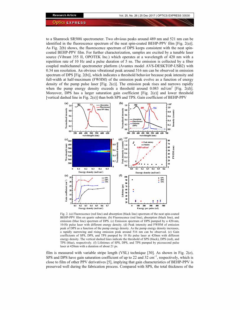
to a Shamrock SR500i spectrometer. Two obvious peaks around 489 nm and 521 nm can be identified in the fluorescence spectrum of the neat spin-coated BEHP-PPV film [Fig. 2(a)]. As Fig. 2(b) shows, the fluorescence spectrum of DPS keeps consistent with the neat spin-coated BEHP-PPV film. For further characterization, samples are excited by a tunable laser source (Vibrant 355 II, OPOTEK Inc.) which operates at a wavelength of 420 nm with a repetition rate of 10 Hz and a pulse duration of 5 ns. The emission is collected by a fiber coupled multichannel spectrometer platform (Avantes model AVS-DESKTOP-USB2) with 0.34 nm resolution. An obvious vibrational peak around 516 nm can be observed in emission spectrum of DPS [Fig. 2(b)], which indicates a threshold behavior because peak intensity and full-width at half-maximum (FWHM) of the emission peak evolve as a function of energy density of the pump pulse laser [Fig. 2(c)]. The emission peak rises and narrows rapidly when the pump energy density exceeds a threshold around 0.083 mJ/cm2 [Fig. 2(d)]. Moreover, DPS has a larger saturation gain coefficient [Fig. 2(e)] and lower threshold [vertical dashed line in Fig. 2(e)] than both SPS and TPS. Gain coefficient of BEHP-PPV
Fig. 2. (a) Fluorescence (red line) and absorption (black line) spectrum of the neat spin-coated BEHP-PPV film on quartz substrate. (b) Fluorescence (red line), absorption (black line), and emission (blue line) spectrum of DPS. (c) Emission spectrum of DPS pumped by a 420-nm, 10-Hz pulse laser with different energy density. (d) Peak intensity and FWHM of emission peak of DPS as a function of the pump energy density. As the pump energy density increases, a rapidly narrowing and rising emission peak around 516 nm can be observed. (e) Gain coefficients of SPS, DPS, and TPS pumped by 10 Hz pulse laser at 420nm with different energy density. The vertical dashed lines indicate the threshold of SPS (black), DPS (red), and TPS (blue), respectively. (f) Lifetimes of SPS, DPS, and TPS pumped by picosecond pulse laser at 420nm with a duration of about 21 ps.
film is measured with variable stripe length (VSL) technique [30]. As shown in Fig. 2(e), SPS and DPS have gain saturation coefficient of up to 22 and 32 cm−1, respectively, which is close to film of other PPV derivatives [5], implying that gain characteristics of BEHP-PPV is preserved well during the fabrication process. Compared with SPS, the total thickness of the
Vol. 25, No. 26 | 25 Dec 2017 | OPTICS EXPRESS 33530
active polymer film in DPS is larger, leading to stronger absorption and emission. However, surface of a spin-coating PPV film could not be completely smooth, especially for the film prepared with toluene [31]. Because the center of our spin-coated film is thicker than the edge, as structure period increases, the quality of spin-coated BEHP-PPV film and SiNx layer decreases, leading to the drop of gain coefficient of TPS compared to that of DPS [Fig. 2(e)].
Lifetimes of samples are measured with an imaging spectrograph (C5094, HAMAMATSU) and a streak camera system (High speed streak unit M1952, HAMAMATSU), pumped by a Nd:YAG laser (EKSPLAPL2143 B/SS) and an OPG system (EKSPLA PG401SH/DFG2-10) operating at the wavelength of 420 nm with a repetition rate of 10 Hz and a pulse duration of 21 ps. As Fig. 2(f) shows, the lifetime of all samples stabilizes to around 23 ps as energy per pulse of the pump laser increases. In addition, photoluminescence (PL) quantum efficiency of BEHP-PPV before and after SiNx deposition is measured with a transient fluorescence spectrometer (FLS 980, EDINBURGH Instrument). Although the PL quantum efficiency of BEHP-PPV film slightly decreases from 7.07% to 6.16% as a result of SiNx deposition, the gain property and uniformity of the lifetime among SPS, DPS and TPS indicate that BEHP-PPV in the hybrid structure remains stable after our process flow.
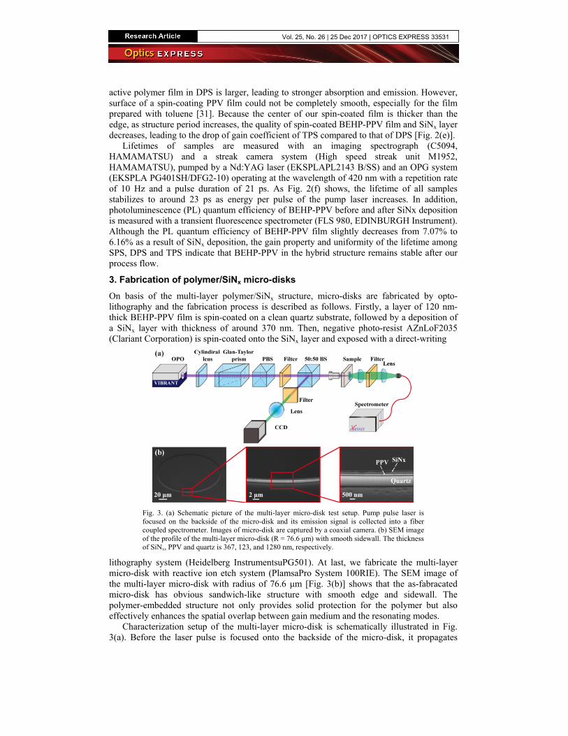
3. Fabrication of polymer/SiNx micro-disks On basis of the multi-layer polymer/SiNx structure, micro-disks are fabricated by opto-lithography and the fabrication process is described as follows. Firstly, a layer of 120 nm-thick BEHP-PPV film is spin-coated on a clean quartz substrate, followed by a deposition of a SiNx layer with thickness of around 370 nm. Then, negative photo-resist AZnLoF2035 (Clariant Corporation) is spin-coated onto the SiNx layer and exposed with a direct-writing
Fig. 3. (a) Schematic picture of the multi-layer micro-disk test setup. Pump pulse laser is focused on the backside of the micro-disk and its emission signal is collected into a fiber coupled spectrometer. Images of micro-disk are captured by a coaxial camera. (b) SEM image of the profile of the multi-layer micro-disk (R = 76.6 μm) with smooth sidewall. The thickness of SiNx, PPV and quartz is 367, 123, and 1280 nm, respectively.
lithography system (Heidelberg InstrumentsuPG501). At last, we fabricate the multi-layer micro-disk with reactive ion etch system (PlamsaPro System 100RIE). The SEM image of the multi-layer micro-disk with radius of 76.6 μm [Fig. 3(b)] shows that the as-fabracated micro-disk has obvious sandwich-like structure with smooth edge and sidewall. The polymer-embedded structure not only provides solid protection for the polymer but also effectively enhances the spatial overlap between gain medium and the resonating modes.
Characterization setup of the multi-layer micro-disk is schematically illustrated in Fig. 3(a). Before the laser pulse is focused onto the backside of the micro-disk, it propagates
Vol. 25, No. 26 | 25 Dec 2017 | OPTICS EXPRESS 33531

through a cylindrical lens, a Glan-Taylor prism, a polarization beam splitter, a 450-nm-centered band-pass filter and a 50:50 beam splitter. A lens collects the signals emitted from the micro-disk into the fiber-coupled spectrometer while images of the micro-disk are captured by a CMOS camera (Thorlabs, Inc). Here, we fabricate six groups of micro-disks with different radii, 52.3, 76.6, 104.6,156.9, 209.2, and 261.5 μm. Photograph of the whole sample under UV light illumination [Fig. 4(a)] shows that BEHP-PPV in the sample can still emit strong fluorescence. Fluorescence spectrum of the micro-disk with radius of 261.5 nm under 405 nm light illumination [Fig. 4(b)] keeps consistence with the neat spin-coated BEHP-PPV film [Fig. 2(a)]. Moreover, when pumped by the 420-nm and 10-Hz laser pulses, ASE can be observed in every group of micro-disks. As for the micro-disk with radius of 261.5 μm, there is an emission peak around 516 nm [Fig. 4(c)]. On the one hand, the emission peak rises rapidly when pump energy density exceeds 6.61 mJ/cm2, indicating a threshold behavior [Fig. 4(d)]. On the other hand, this emission peak blue shifts slightly as the pump density increases, which is related with the self-absorption of BEHP-PPV film. Compared with micro-disk with radius of 52.3 μm, micro-disk with radius 261.5 μm shows more obvious threshold behavior and thus has higher gain.
Fig. 4. (a) Photograph of six groups of micro-disks under UV light illumination. (b) Fluorescence spectrum of the micro-disk with radius of 261.5 μm. (c) Emission spectrum of micro-disk with radius of 261.5 μm pumped by a 420-nm and 10-Hz pulse laser with different energy density. The inset picture shows the micro-disk under white light illumination (top) and the pulse laser pump (bottom). (d) Peak intensity of the emission peaks of micro-disks with radius of 261.5 and 52.3 μm, respectively, indicating a threshold around 6.61 mJ/cm2 for the micro-disk with its radius of 261.5 μm.
4. Conclusion We have fabricated an organic/inorganic hybrid structure consisting of spin-coated BEHP-PPV film and SiNx layer. During the whole fabrication processes, activity of BEHP-PPV in the hybrid structure shows no obvious degradation. Typically, saturation gain coefficient of DPS sample can be up to 32 cm−1. Then we fabricate six groups of multi-layer hybrid micro-disks with different radius on the basis of such hybrid structure and ASE is observed when the micro-disks are pumped by nanosecond laser pulses. Thus, optical properties of BEHP-PPV remain stable in the hybrid structure and the micro-disk, which indicates that the organic/inorganic hybrid structure could provide a new platform for constructing novel hybrid integrated components in many photonic applications.
Vol. 25, No. 26 | 25 Dec 2017 | OPTICS EXPRESS 33532

Funding National Natural Science Foundations of China (51403244, 61323001, 11774437, 11474365); Natural Science Foundation of Guangdong Province (2014A030313104); Science and Technology Program of Guangzhou (201707020017, 2018-1002-SF-0094); Fundamental Research Funds for the Central Universities of China (Sun Yat-sen University: 17lgzd06, 16lgjc16).
Acknowledgments We thank Prof. Bingjia Xu from South China Normal University for the assistance of the measurement on the PL quantum efficiency of our fabricated samples.
Vol. 25, No. 26 | 25 Dec 2017 | OPTICS EXPRESS 33533


![DEVICE OPERATION OF POLYMER LIGHT-EMITTING … Bound... · DEVICE OPERATION OF POLYMER LIGHT-EMITTING DIODES ... and Ca asan electron injector. ... in disordered materials [13] ...](https://static.fdocuments.in/doc/165x107/5a9e077d7f8b9a39338be6c2/device-operation-of-polymer-light-emitting-bounddevice-operation-of-polymer.jpg)