HYBRID DYNAMIC PHASE ALIGNMENT SCHEME TO … · menggunakan konsep berbilang fasa yang sedia adadan...
24
HYBRID DYNAMIC PHASE ALIGNMENT SCHEME TO IMPROVE SAMPLING RESOLUTION FOR 1.25 GHZ SOURCE SYNCHRONOUS INTERFACE By LIM KOK CHEAN A Dissertation submitted for partial fulfillment of the requirements for the degree of Master of Science July 2013
-
Upload
nguyenkhanh -
Category
Documents
-
view
219 -
download
0
Transcript of HYBRID DYNAMIC PHASE ALIGNMENT SCHEME TO … · menggunakan konsep berbilang fasa yang sedia adadan...

HYBRID DYNAMIC PHASE ALIGNMENT SCHEME TO IMPROVE SAMPLING
RESOLUTION FOR 1.25 GHZ SOURCE SYNCHRONOUS INTERFACE
By
LIM KOK CHEAN
A Dissertation submitted for partial fulfillment of the
requirements for the degree of Master of Science
July 2013

ii
Acknowledgement
First and foremost, I would like to thank my supervisor, Dr. Zuraini bt. Dahari, for
giving me the opportunity to work under her. Her sound advice and expert guidance
throughout the dissertation is invaluable. I would like to dedicate this section to my
friends and colleagues who have assisted in the course of writing this project. Their
remarkable talents and special skills assured this project of clarity and completeness.
Also, I would like to thank my family, who has shown remarkable patience,
encouragement and understanding while I was pursuing my research. Last but not
least, I reserve my sincere appreciation for the people that are not mentioned above,
who had helped me in this research and enabled the thesis to be done on time.

iii
Table of Contents Acknowledgement ............................................................................................................... ii Table of Contents ............................................................................................................... iii List of Figures ...................................................................................................................... v List of Tables .................................................................................................................... viii List of Abbreviations .......................................................................................................... ix Abstrak ................................................................................................................................ x Abstract ............................................................................................................................... xi CHAPTER 1 ........................................................................................................................ 1 INTRODUCTION ............................................................................................................... 1
1.1 Background ............................................................................................................... 1 1.2 Problem Statements ................................................................................................... 2 1.3 Objective ................................................................................................................... 4 1.4 Project Scopes ........................................................................................................... 4 1.5 Research Contribution ............................................................................................... 5 1.6 Thesis Organization ................................................................................................... 5
CHAPTER 2 ........................................................................................................................ 7 LITERATURE REVIEW ................................................................................................... 7
2.1 Evolution of Serial Interface ..................................................................................... 7 2.1.1 Parallel Interface ............................................................................................. 7 2.1.2 High Speed Parallel Interface ......................................................................... 9 2.1.3 Migration to Serial Interface ........................................................................ 10
2.2 Serial Interface Design ............................................................................................ 11 2.2.1 Asynchronous Serial Interface Design ......................................................... 11 2.2.2 Source Synchronous Serial Interface Design ............................................... 12 2.2.3 Timing Consideration for Serial Interface .................................................... 15
2.3 DPA Architecture and Design ................................................................................. 18 2.3.1 Multi-Phase Sampling Scheme ..................................................................... 18 2.3.2 Multi-Tap Delay Line Sampling Scheme ..................................................... 23
2.4 Proposed Hybrid Dynamic Phase Alignment Scheme ............................................ 27 2.5 Chapter Summary .................................................................................................... 28
CHAPTER 3 ...................................................................................................................... 29 DESIGN METHODOLOGY AND IMPLEMENTATION ............................................. 29
3.1 Block Diagram of Proposed Hybrid Sampling Block ............................................. 29 3.2 Flow Chart of Proposed Hybrid Sampling Block ................................................... 31
3.2.1 Multi-phase sampling technique ................................................................... 33 3.2.2 Multi-tap delay line sampling flow .............................................................. 35
3.3 System Level Implementation ................................................................................. 37 3.4 Multi-Phase Sampling Block Implementation ........................................................ 40
3.4.1 Phase Detector .............................................................................................. 40 3.4.2 Counter ......................................................................................................... 44 3.4.3 Clock Multiplexer ......................................................................................... 47 3.4.4 Controller ...................................................................................................... 51

iv
3.4.5 Integration of Multi-Phase Sampling Block ................................................. 53 3.5 Multi-Tap Delay Line Sampling Block Implementation ........................................ 55
3.5.1 Skew Measure Block .................................................................................... 55 3.5.2 Delay Line .................................................................................................... 58 3.5.3 LOCK Signal Generator ............................................................................... 59 3.5.4 Integration of Multi-Tap Delay Line Sampling Block ................................. 61
3.6 Proposed Hybrid Dynamic Alignment Circuit ........................................................ 64 3.7 Chapter Summary .................................................................................................... 65
CHAPTER 4 ...................................................................................................................... 67 RESULTS AND DISCUSSION ....................................................................................... 67
4.1 Simulation Strategy and Result ............................................................................... 67 4.1.1 Test 1-8: Hybrid Design Functionality and Clock Phase Coverage ............. 68 4.1.2 Test 9-12: Delay Line Coverage ................................................................... 77 4.1.3 Test 13-14: Continuous Monitoring Coverage ............................................. 80
4.2 Test Result Discussion ............................................................................................ 83 4.3 Chapter Summary .................................................................................................... 87
CHAPTER 5 ...................................................................................................................... 88 CONCLUSION AND RECOMMENDATIONS ............................................................. 88
5.1 Conclusions ............................................................................................................. 88 5.2 Future Recommendations ........................................................................................ 90
REFERENCE .................................................................................................................... 91 APPENDIX A ................................................................................................................... 94

v
List of Figures
Figure 2.1: I/O Trends for Semiconductor Devices (Holden, Andresakis et al.,
2009) .................................................................................................................... 8
Figure 2.2: Data Recovery with PLL (Allen, 2003) .................................................. 12
Figure 2.3: Simple Source Synchronous Interface .................................................... 13
Figure 2.4: Block Diagram of Source Synchronous Interface System (Burney, Xu et al., 2009) .................................................................................................. 14
Figure 2.5: Source of Skew, Jitter and Noise in Source Synchronous System (Altera Corporation, 2004) ................................................................................ 16
Figure 2.6: System Timing Budget for Source Synchronous Interface (Altera Corporation, 2004)............................................................................................. 17
Figure 2.7: Optimal Sampling Point (Chang and Starr, 2009; Kubicek and Kolka, 2010) .................................................................................................................. 17
Figure 2.8: Multi-phase Sampling Scheme (Burney, 2010) ...................................... 19
Figure 2.9: Block Diagram for Multi-phase Sampling Scheme (Chang and Starr, 2009) .................................................................................................................. 20
Figure 2.10: True Table of Phase Detector (Chang and Starr, 2009) ........................ 21
Figure 2.11: Block Diagram for Multi-Tap Delay Line (Yeoh, 2009) ...................... 24
Figure 2.12 : Block Diagram of Delay Module (Yeoh, 2009) .................................. 24
Figure 2.13: Timing Diagram illustrating the Monitor Window (Yeoh, 2009) ........ 26
Figure 2.14: Delay Module Tap Sweep (Robert Le, 2011) ....................................... 27
Figure 3.1: Hybrid Dynamic Alignment Block Diagram .......................................... 30
Figure 3.2: Flowchart of the Proposed Hybrid Sampling Block ............................... 33
Figure 3.3: Flow Chart for Multi-Phase Sampling Technique .................................. 35
Figure 3.4: Flow Chart for Multi-Tap Delay Line Sampling .................................... 37
Figure 3.5: System Level Implementation for the Proposed Hybrid Block .............. 40
Figure 3.6: Comparison of Linear and Non-Linear Phase Detector (Forcan, 2007) .................................................................................................................. 42
Figure 3.7: Schematic of Bang-Bang Phase Detector ............................................... 43
Figure 3.8: Phase Detector's Output in Different Scenarios ...................................... 44
vi
Figure 3.9: Schematic of Counter .............................................................................. 46
Figure 3.10: Schematic of Clock Multiplexer (Top Level) ....................................... 48
Figure 3.11:Schematic of Clock Selection (Sub-Block) ........................................... 48
Figure 3.12: Schematic of Clock Selection Block ..................................................... 49
Figure 3.13: Schematic of Clock Multiplex Block (Top-Level) ............................... 50
Figure 3.14: Schematic of Clock Multiplex Block (Sub-Block) ............................... 50
Figure 3.15: Schematic of Controller (Top Level) .................................................... 52
Figure 3.16: Schematic of Controller (Counter 1 Logic) .......................................... 52
Figure 3.17: Schematic of Controller (Counter 2 Logic) .......................................... 53
Figure 3.18: Integration of Multi-Phase Sampling Block ......................................... 54
Figure 3.19: Schematic of Skew Measure Block ...................................................... 57
Figure 3.20: Timing Diagram of Skew Measure Block ............................................ 58
Figure 3.21: Schematic of Single Delay Line ........................................................... 59
Figure 3.22: Schematic of Full Delay Line ............................................................... 59
Figure 3.23: State Machine used by LOCK Signal Generator .................................. 60
Figure 3.24: Schematic of LOCK Signal Generator ................................................. 61
Figure 3.25: Schematic of Delay Tap Adjustment Block .......................................... 63
Figure 3.26: Schematic of Proposed Hybrid Dynamic Phase Alignment Block ....... 66
Figure 4.1: Result of Test 1. a) Selected Clock Phase. b) SWITCH & SHIFT Signals c) Lock Signals. d) Input Data .......................................................... 69
Figure 4.2: Skew Difference between Data and Clock (Test 1). a) Initial Skew. b) Skew from the Multi-Tap Delay Line Sampling Block. c) Sampled Data from Multi-Phase Sampling Block. d) Skew from Multi-Phase Sampling Block. ................................................................................................................. 70
Figure 4.3: Result of Test 2. a) Selected Clock Phase. b) Lock Signals. c) Skew from Multi-Phase Sampling Block. d) Skew from Multi-Tap Delay Line Sampling Block ................................................................................................. 71
Figure 4.4: Result of Test 3. a) Selected Clock Phase. b) Lock Signals. c) Skew from Multi-Phase Sampling Block. d) Skew from Multi-Tap Delay Line Sampling Block ................................................................................................. 72
vii
Figure 4.5: Result of Test 4. a) Selected Clock Phase. b) Lock Signals. c) Skew from Multi-Phase Sampling Block. d) Skew from Multi-Tap Delay Line Sampling Block ................................................................................................. 73
Figure 4.6: Result of Test 5. a) Selected Clock Phase. b) Lock Signals. c) Skew from Multi-Phase Sampling Block. d) Skew from Multi-Tap Delay Line Sampling Block ................................................................................................. 74
Figure 4.7: Result of Test 6. a) Selected Clock Phase. b) Lock Signals. c) Skew from Multi-Phase Sampling Block. d) Skew from Multi-Tap Delay Line Sampling Block ................................................................................................. 75
Figure 4.8: Result of Test 7. a) Selected Clock Phase. b) Lock Signals. c) Skew from Multi-Phase Sampling Block. d) Skew from Multi-Tap Delay Line Sampling Block ................................................................................................. 76
Figure 4.9: Result of Test 8. a) Selected Clock Phase. b) Lock Signals. c) Skew from Multi-Phase Sampling Block. d) Skew from Multi-Tap Delay Line Sampling Block ................................................................................................. 77
Figure 4.10: Result of Test 9. a) Selected Clock Phase. b) Lock Signals. c) Skew from Multi-Tap Delay Line Sampling Block .................................................... 78
Figure 4.11: Result of Test 10. a) Selected Clock Phase. b) Lock Signals. c) Skew from Multi-Tap Delay Line Sampling Block .......................................... 79
Figure 4.12: Result of Test 11. a) Selected Clock Phase. b) Lock Signals. c) Skew from Multi-Tap Delay Line Sampling Block .......................................... 79
Figure 4.13: Result of Test 12. a) Selected Clock Phase. b) Lock Signals. c) Skew from Multi-Tap Delay Line Sampling Block .......................................... 80
Figure 4.14: Result of Test 13. a) Selected Clock Phase. b) Lock Signals. c) Skew from Multi-Phase Sampling Block. d) Skew from Multi-Tap Delay Line Sampling Block ......................................................................................... 82
Figure 4.15: Result of Test 14. a) Selected Clock Phase. b) Lock Signals. c) Skew from Multi-Phase Sampling Block. d) Skew from Multi-Tap Delay Line Sampling Block ......................................................................................... 83

viii
List of Tables
Table 2.1: Comparison of Gigabit Ethernet Designs ................................................. 11
Table 2.2 : Comparison of Multi-Phase and Multi-Tap Delay Line Sampling Scheme............................................................................................................... 28
Table 3.1: True Table for Bang-Bang Phase Detector .............................................. 42
Table 3.2: True Table for the Clock Selection Block ................................................ 48
Table 3.3: Delay Tap Selection ................................................................................. 59
Table 3.4: Port List for the Proposed Hybrid Circuit ................................................ 64
Table 4.1: Result Summary of Test 1 to Test 8 ......................................................... 84
Table 4.2: Summary of Results for Test 9 to 12 ........................................................ 84
Table 5.1: Sampling Resolution Comparison across Different Sampling Scheme ... 89
ix
List of Abbreviations
Abbreviation Meaning 8B/10B 8 bits/10 bits BBPD Bang-Bang Phase Detector CDR Clock and Data Recovery DC Direct Current DFF D Flip-Flop DLL Delay Lock Loop DPA Dynamic Phase Alignment EMI Electromagnetic Interference FIFO First In First Out Gbps Giga bits per second GMII Gigabit Media Independent Interface I/O Input/output LPF Low Pass Filter LVCMOS Low Voltage Complementary Metal Oxide Semiconductor LVDS Low Voltage Differential Signaling LVTTL Low Voltage Transistor-Transistor Logic MHz Mega Hertz PCB Printed Circuit Board PD Phase Detector PLL Phase Lock Loop PnR Place and Route PRBS Pseudo Random Binary Sequence ps pico second PVT Process, Voltage and Temperature RGMII Reduced Gigabit Media Independent Interface Rx Receive SEIO Single Ended Input/Output SerDes Serializer/Deserializer SGMII Serial Gigabit Media Independent Interface TSMC Taiwan Semiconductor Manufacturing Company TTL Transistor-Transistor Logic Tx Transmit TT Typical-Typical UI Unit Interval VCO Voltage Controlled Oscillator
x
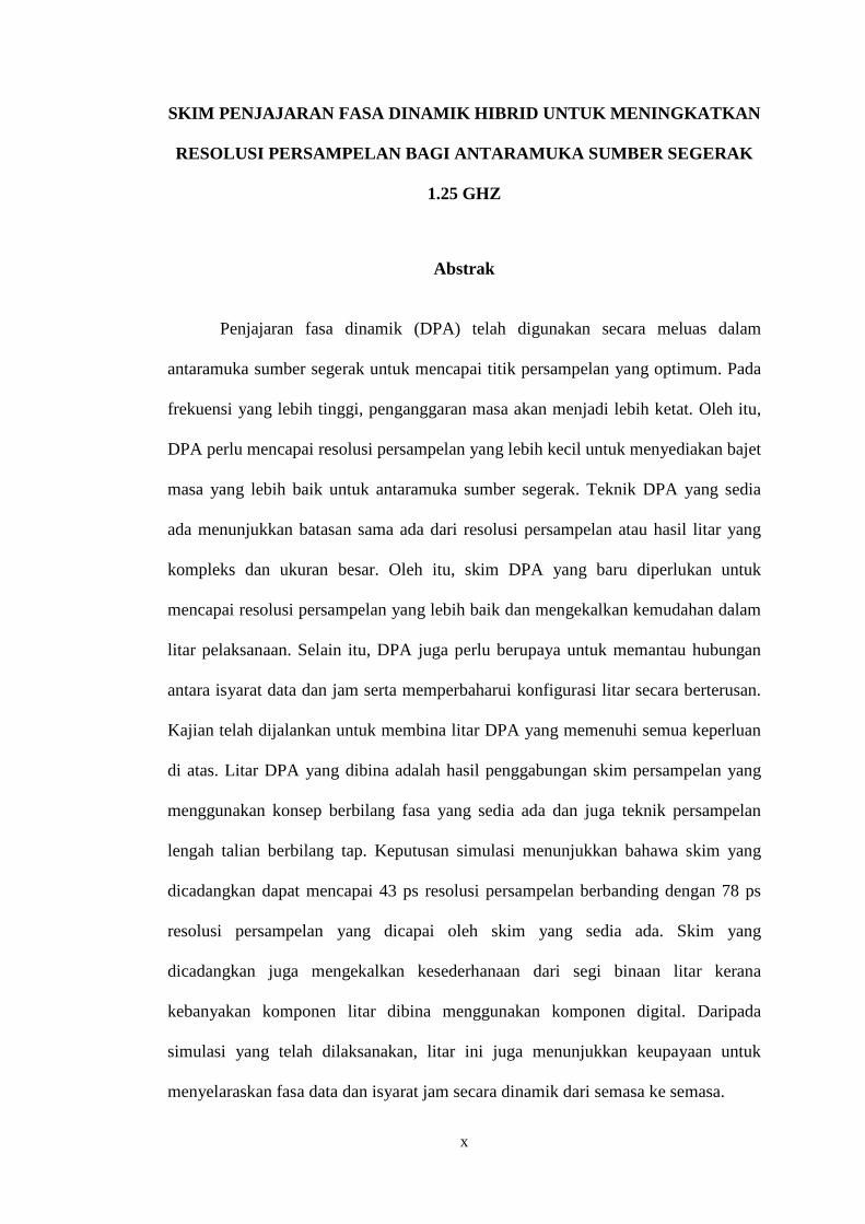
SKIM PENJAJARAN FASA DINAMIK HIBRID UNTUK MENINGKATKAN
RESOLUSI PERSAMPELAN BAGI ANTARAMUKA SUMBER SEGERAK
1.25 GHZ
Abstrak
Penjajaran fasa dinamik (DPA) telah digunakan secara meluas dalam
antaramuka sumber segerak untuk mencapai titik persampelan yang optimum. Pada
frekuensi yang lebih tinggi, penganggaran masa akan menjadi lebih ketat. Oleh itu,
DPA perlu mencapai resolusi persampelan yang lebih kecil untuk menyediakan bajet
masa yang lebih baik untuk antaramuka sumber segerak. Teknik DPA yang sedia
ada menunjukkan batasan sama ada dari resolusi persampelan atau hasil litar yang
kompleks dan ukuran besar. Oleh itu, skim DPA yang baru diperlukan untuk
mencapai resolusi persampelan yang lebih baik dan mengekalkan kemudahan dalam
litar pelaksanaan. Selain itu, DPA juga perlu berupaya untuk memantau hubungan
antara isyarat data dan jam serta memperbaharui konfigurasi litar secara berterusan.
Kajian telah dijalankan untuk membina litar DPA yang memenuhi semua keperluan
di atas. Litar DPA yang dibina adalah hasil penggabungan skim persampelan yang
menggunakan konsep berbilang fasa yang sedia ada dan juga teknik persampelan
lengah talian berbilang tap. Keputusan simulasi menunjukkan bahawa skim yang
dicadangkan dapat mencapai 43 ps resolusi persampelan berbanding dengan 78 ps
resolusi persampelan yang dicapai oleh skim yang sedia ada. Skim yang
dicadangkan juga mengekalkan kesederhanaan dari segi binaan litar kerana
kebanyakan komponen litar dibina menggunakan komponen digital. Daripada
simulasi yang telah dilaksanakan, litar ini juga menunjukkan keupayaan untuk
menyelaraskan fasa data dan isyarat jam secara dinamik dari semasa ke semasa.

xi
HYBRID DYNAMIC PHASE ALIGNMENT SCHEME TO IMPROVE
SAMPLING RESOLUTION FOR 1.25 GHZ SOURCE SYNCHRONOUS
INTERFACE
Abstract
Dynamic phase alignment (DPA) circuit has been widely used in source
synchronous interface to achieve an optimal sampling point. At higher frequency,
the timing requirement will become more stringent. Therefore, the DPA circuit
needs to achieve finer sampling resolution to provide a better timing budget for the
source synchronous interface. Existing DPA techniques have shown the limitation
either on the sampling resolution or potentially large and complex circuit
implementation. Due to this, a new DPA scheme is needed in order to achieve better
sampling resolution and at the same time keep the simplicity in the circuit
implementation. Beside the timing consideration, DPA also need to be able to
monitor relation between the data and clock continuously and adjust the setting
dynamically. A study has been conducted to develop an improved version of DPA
circuit that meets all the requirements above. The improved DPA circuit is
implemented by combining the existing multi-phase sampling scheme and also the
multi-tap delay line sampling technique. Simulation results show that the proposed
design able to achieve 43 ps sampling resolution compares to 78 ps sampling
resolution achieves by the existing scheme. The proposed design keeps the
simplicity of the circuit by using the digital blocks to construct most of the circuit
components. From the performed simulations, the circuit also shows the capability
to dynamically phase align the data and clock signals from time to time.

1
CHAPTER 1
INTRODUCTION
1.1 Background
Serial data transmission is used in the majority of today’s interconnect and
data transmission system due to its simplicity and minimum hardware requirement.
This is especially true with the explosion of data, voice and video traffic across
many markets. The serial data interface can be divided into asynchronous
transmission and also synchronous transmission.
For asynchronous serial transmission, only data bits sent from the
transmission source to the receiver end. A clock and data recovery block (CDR) is
normally used to regenerate the clock signal from the data stream and used it to
sample the incoming data bits. Plenty of solutions have been invented but most of
today’s CDR system is implemented using phase-locked loop (PLL) and delay lock
loop (DLL) circuitry (Lee and Bulzacchelli, 1992; Sang-Ho, Hyung-Min et al.,
2010).
As for synchronous serial transmission, a reference clock is sent together
with the data from the transmission source. For these source-synchronous interfaces,
clock and data signals skew need to be kept minimum. Keeping the clock and data
signals phase aligned can be difficult when dealing with the board, package and on-
2
die effects such as skew, jitter, and noise (Altera Corporation, 2004). In order to
minimize such effects, a phase alignment scheme is needed to achieve high
bandwidth applications.
Phase alignment can be categorized into 2 main groups: static phase
alignment and dynamic phase alignment (DPA). For static phase alignment, designer
need to carefully match the data and the clock path on the board, package and also
on-die routing. This approach is labor-intensive, time consuming and difficult due to
the today’s high pin count device (Altera Corporation, 2004). On the other side,
DPA have been developed to improve the static phase alignment method. DPA
block will realign the incoming data with respect to the clock edge. The clock edge
will shift to the center of the data eye which in return increase the timing margin of a
system and result in higher bandwidth support (Khor, Hoo et al., 2007). DPA system
will normally perform a multiple data stream sampling before the circuitry can find
out the optimal clock phase or delay setting used to realign the data and clock
signals. The routing mismatch between the data and clock path for each receiver
channel can be compensated by the DPA block individually and automatically if the
DPA blocks being integrated into each receiver channel (Venkata, Wong et al.,
2003). The designers can save the effort from manually match the routing skew for
each pin and accelerating the time to market for new products by doing this.
1.1.1 Problem Statements
Timing budget is the account of timing requirements or timing parameters
necessary for a system to function properly. For source synchronous interface design,
the timing requirement must fit within a single clock cycle. The timing parameters

3
involve many factors, including setup and hold time requirement, channel to channel
skew requirement, jitter performance and also maximum operating frequency
requirement. For an ideal case scenario, the clock signal need to sample the data at
the exact center point of the data bit interval in order to obtain a maximum timing
margin for the mentioned timing parameters. The timing margin introduces by
multi-phase sampling scheme described in (Chang and Starr, 2009) and (Burney,
2010) is limited by the number of clock phases provided by PLL. Increase the
number of clock phase can achieve better sampling resolution. However, there is a
tradeoff for increasing the clock phases as the complexity of PLL design will
increase accordingly.
On the other hand, multi-tap delay line sampling scheme described in (Yeoh,
2009) may provide better sampling resolution than the PLL-based dynamic phase
adjustment circuit. The improved sampling resolution is achieved by using delay
elements with small propagation delay for each delay tap. However, since the data
and the clock signal phase relation are unknown for source synchronous interface, a
large set of delay elements need to be built in order to compensate for a full clock
cycle period. As the result, the total number of delay elements and the associated
logic could force the dynamic phase alignment circuit to be quite huge.
In short, both dynamic phase alignment schemes showing disadvantage
either on the sampling resolution or large and complex circuit design. Therefore, a
new dynamic phase adjustment circuit is needed to achieve better sampling
resolution without being inordinately large and complex.
4
1.2 Objective
This research will propose a new hybrid dynamic phase alignment circuit which
will be used on the receiver side of source synchronous interface. The proposed
circuit combines both the multi-phase and multi-tap delay line sampling schemes.
This research has the following objectives:
1. To investigate a suitable dynamic phase alignment scheme to be used in
source synchronous interface.
2. To propose a hybrid phase alignment scheme at the receiver side to achieve
better sampling resolution compare to existing multi-phase sampling scheme
and multi-tap delay line sampling scheme.
3. To achieve real time dynamic alignment to compensate for any data to clock
skew from time to time.
1.3 Project Scopes
The receiver for source synchronous serial interface contains input pins,
sampling units and also the deserializer. The scope of this research will only focus
on the software implementation of the sampling unit. The sampling unit will be
implemented using both multi-phase and multi-tap delay line sampling schemes.
The target performance of this circuit is 1.25 GHz toggle rates.

5
1.4 Research Contribution
This project will contribute a new dynamic phase alignment scheme by
combining the existing multi-phase and multi-tap delay line sampling schemes. The
proposed dynamic phase alignment circuit can be used to sample the incoming data
at the receiver side of the serial interface. This new method will improve the
sampling resolution over the traditional multi-phase sampling scheme and at the
same time maintain the simplicity compare to the conventional delay tap sampling
scheme.
1.5 Thesis Organization
The remainder of this thesis is organized into four chapters as follows.
Chapter 2 discusses relevant literature review focusing on the two main phase
alignment scheme which is a multi-phase sampling and also the multi-tap delay line
sampling schemes. The chapter begins by showing the evolution of the serial
interface system and also the issues and concerns regarding the serial interface
implementation. Examples of the multi-phase sampling circuit and multi-tap delay
line sampling circuit used in industry will be presented and discussed in detail.
Chapter 3 discussed the development of the proposed dynamic phase
alignment circuit. This chapter will be break down according to each sub-module
built in the dynamic phase alignment circuit. The functionality and implementation
for each sub-module will be discussed in detail. This chapter concludes with a
combination of all the sub-modules to form a complete dynamic phase alignment
system.
6
Chapter 4 discusses and analyses the simulation and measurement results.
This chapter starts off with the introduction to the software tools and technology
process used in this project. It is continued with the functionality and timing result
verification to ensure the built logic behaves and function correctly.
The final chapter, Chapter 5 consists of conclusions and future works. The
conclusion will cover the key highlights of the findings and contributions of the
research while some recommendations and ideas for future works are proposed.
7
CHAPTER 2
LITERATURE REVIEW
Chapter 1 explains the necessity and also the advantages of implementing the
DPA block inside the source synchronous interface design. The current DPA designs
show limitation either on the sampling resolution or the complexity in the circuit
implementation. Therefore a hybrid DPA scheme has been proposed to achieve
better sampling resolution and reduce the complexity in the circuit implementation.
To complement the first chapter, Chapter 2 presents the prior art design that used for
the source synchronous interface and the literature review that relates to the existing
DPA architecture.
2.1 Evolution of Serial Interface
This section will discuss the development of serial interface in the industry.
The section will be concluded by using the Gigabit Ethernet as an example to show
the evolution of the serial interface.
2.1.1 Parallel Interface
In the earlier system design, the simplest method of data transmission across
different chip is to directly connect the data path from one chip to the next chip in
the parallel format. The data path often consists more than one bit of information to
form a system interface. For a complex interface design, hundred of pins may be
8
required in order to transfer the information from one chip to another chip. This also
raises the issue on how many input/output (I/O) pins that can be fit into a single
chip. Due to the Moore’s Law prediction, more and more circuits can be
manufactured into a single chip compare few decades ago. However, pin density of
chip packaging has not increased at the same rate as the silicon density which
creates a scenario where the package I/O pins are more expensive than silicon
circuits (Stauffer, 2008). Besides the package consideration, printed circuit board
(PCB) design also shows cost increasing due to the excessive pin count that take up
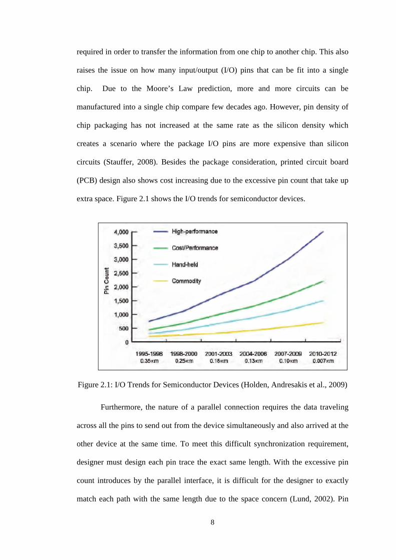
extra space. Figure 2.1 shows the I/O trends for semiconductor devices.
Figure 2.1: I/O Trends for Semiconductor Devices (Holden, Andresakis et al., 2009) Furthermore, the nature of a parallel connection requires the data traveling
across all the pins to send out from the device simultaneously and also arrived at the
other device at the same time. To meet this difficult synchronization requirement,
designer must design each pin trace the exact same length. With the excessive pin
count introduces by the parallel interface, it is difficult for the designer to exactly
match each path with the same length due to the space concern (Lund, 2002). Pin
9
trace of differing length creates channel skew which can directly degrade the
interface transfer rate.
2.1.2 High Speed Parallel Interface
The issue of integrated excessive pin count into a single device will become
more significant over time as shown in Figure 2.1. A simple way to correct this
problem is to use fewer pins. In order to achieve this goal, designer started to push
the interface toggle rate to much higher speed. With higher toggle rate, same amount
of data can be completely sent to the destination by using fewer pin. This approach
offers some advantages but does not solve all of the issues arise from using the
parallel interface. Fewer pins reduce the package and the PCB cost which makes the
designs more competitively priced. On top of that, few pins make it easier to
synchronize all the signals so the data can be sent and received synchronously.
However, the increase of frequency for each trace results some trade off. One
of the concerns is the electromagnetic interference (EMI) between the traces. The
EMI is caused by the Single Ended I/O (SEIO) standard used by the parallel
interface. An example of the SEIO standard used in the industry is Low Voltage
Transistor-Transistor Logic (LVTTL) and Low Voltage Complementary Metal
Oxide Semiconductor (LVCMOS) (JEDEC, 2006). These standards will create
interference issues due to the higher current inject into each trace as the result of
higher toggle rate (Lund, 2002; Bogatin, 2004). The signal integrity issue caused by
the EMI can degrade or limit the effective performance of the circuit. This problem
can be solved by adding more space between the traces or fully shield each and

10
every trace to eliminate the interference. These approaches defeat the goal of
increasing the pin toggle rates.
2.1.3 Migration to Serial Interface
The next solution to the parallel interface issue is to shift from a parallel
interface to a serial interface. Few data streams will be combined into a single data
stream and send through the interface using much higher speed. At the receiver end,
the data stream will be further broken down to form parallel of signals again before
sending out to the processing unit. These operations normally involve the Serializer
and Deserializer (SerDes) circuitry. One of the important factors that enable this
operation is the used of the Low-Voltage Differential Signaling (LVDS) standard.
The LVDS technology allows the signal transfer at Gigabits per second compare to
the LVTTL/LVCMOS which only allow a few hundred of Megabits per second
transfer rate (Texas Instruments, 2002). Beside the higher toggle rate, the LVDS
standard also help to reduce the EMI due to the field coupling within the differential
pair (Cole, 2002).
Table 2.1 shows the evolution of serial interface using the Gigabit Ethernet
designs as an example. Gigabit Media Independent Interface (GMII) is a standard
used to achieve transfer rates up to 1 Gigabit per second in Ethernet network
(Fifield, 1997). Due to the parallel interface architecture, total 12 receive signals
(Rx) and 12 transmit signals (Tx) are required. To reduce the GMII pin count,
Reduced Gigabit Media Independent Interface (RGMII) has been introduced (Alto,
2002). RGMII uses half the number of data pins as used in the GMII interface. This
reduction is achieved by clocking the data at both rising edge and falling edge of the
11
clock signal. Although the RGMII standard reduced the pin count by half, but this
standard suffers from the EMI issue due to the higher toggle rate. Following the
RGMII standard, Serial Gigabit Media Independent Interface (SGMII) has been
introduced (Chu, 2001). This interface uses the LVDS standard and the transfer rate
can achieve up to 1.25 Gigabit per second. Due to the nature of differential signaling
used by the LVDS standard, the effect of EMI has been greatly reduced. SGMII only
uses single data stream to transfer the data. However due to the differential standard,
2 I/O pins will be used for transmit and receive side.
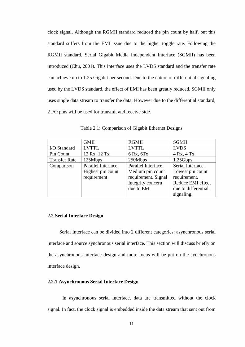
Table 2.1: Comparison of Gigabit Ethernet Designs
GMII RGMII SGMII I/O Standard LVTTL LVTTL LVDS Pin Count 12 Rx, 12 Tx 6 Rx, 6Tx 4 Rx, 4 Tx Transfer Rate 125Mbps 250Mbps 1.25Gbps Comparison Parallel Interface.
Highest pin count requirement
Parallel Interface. Medium pin count requirement. Signal Integrity concern due to EMI
Serial Interface. Lowest pin count requirement. Reduce EMI effect due to differential signaling.
2.2 Serial Interface Design
Serial Interface can be divided into 2 different categories: asynchronous serial
interface and source synchronous serial interface. This section will discuss briefly on
the asynchronous interface design and more focus will be put on the synchronous
interface design.
2.2.1 Asynchronous Serial Interface Design
In asynchronous serial interface, data are transmitted without the clock
signal. In fact, the clock signal is embedded inside the data stream that sent out from

12
the transmitter. A clock data recovery (CDR) circuit is required to extract the clock
information out of the data stream. Figure 2.2 shows the example of clock data
recovery block diagram. The CDR consists of phase lock loop (PLL) and decision
circuit. The PLL consists of phase detector (PD), charge pump, low pass filter (LPF)
and voltage control oscillator (VCO). The PD will detect the clock phase from the
data stream and output the control signal to the VCO to regenerate the clock signal.
The generated clock signal is used to sample the data inside the decision circuit. The
decision circuit will decide if the optimal sampling point has been achieved. Beside
the PLL based CDR circuit, CDR can be implemented through the delay lock loop
(DLL) as well. Example of CDR design based on DLL (Lee and Bulzacchelli,
1992), oversampling technique (Ahmed and Kwasniewski, 2005), and improved
oversampling technique (van Ierssel, Sheikholeslami et al., 2007).
Figure 2.2: Data Recovery with PLL (Allen, 2003)
2.2.2 Source Synchronous Serial Interface Design
In contrast from asynchronous interface, data is transmitted together with the
clock signal in source synchronous serial interface. Therefore the clock recovery
unit is not needed for source synchronous serial interface design. Figure 2.3 shows a
simple source synchronous interface. Since the clock signal is common for

13
transmitter and receiver, designer only need to ensure the traces between data and
clock signals is closely matched in order to get the correct sampling data at the
receiver side.
Figure 2.3: Simple Source Synchronous Interface
In order to minimize the skew difference between the data and clock signals,
a phase alignment scheme has been introduced to achieve high bandwidth
application. As described in Chapter 1, the phase alignment can be categorized into
2 categories which are the static phase alignment and dynamic phase alignment
(DPA). For the static phase alignment, designer have to perform manual work to
ensure the data and clock signals route is closely matched on the die, on the package
and also on board. This work is labor intensive, time consuming and difficult due to
the high pin count device (Altera Corporation, 2004). Furthermore, by using the
static phase alignment the route matching effort needs to be repeated for each new
design.
On the other hand, DPA involve a circuit implementation at the receiver side
to adjust the skew between the data and clock signals. By implementing the DPA
circuit into each receiver channel, the skew between the data and clock signals will
be compensated by the DPA circuit dynamically. Due to this, designers do not need
to spend the effort to optimize each signal path to ensure the routing is matched to