HVEM AND HREM OF INTERFACES IN ALUMINIUM NITRIDE …
7
HAL Id: jpa-00228015 https://hal.archives-ouvertes.fr/jpa-00228015 Submitted on 1 Jan 1988 HAL is a multi-disciplinary open access archive for the deposit and dissemination of sci- entific research documents, whether they are pub- lished or not. The documents may come from teaching and research institutions in France or abroad, or from public or private research centers. L’archive ouverte pluridisciplinaire HAL, est destinée au dépôt et à la diffusion de documents scientifiques de niveau recherche, publiés ou non, émanant des établissements d’enseignement et de recherche français ou étrangers, des laboratoires publics ou privés. HVEM AND HREM OF INTERFACES IN ALUMINIUM NITRIDE CERAMICS S. Hagege, Y. Ishida, S. Tanaka To cite this version: S. Hagege, Y. Ishida, S. Tanaka. HVEM AND HREM OF INTERFACES IN ALUMINIUM NITRIDE CERAMICS. Journal de Physique Colloques, 1988, 49 (C5), pp.C5-189-C5-194. 10.1051/jphyscol:1988518. jpa-00228015
Transcript of HVEM AND HREM OF INTERFACES IN ALUMINIUM NITRIDE …

HAL Id: jpa-00228015https://hal.archives-ouvertes.fr/jpa-00228015
Submitted on 1 Jan 1988
HAL is a multi-disciplinary open accessarchive for the deposit and dissemination of sci-entific research documents, whether they are pub-lished or not. The documents may come fromteaching and research institutions in France orabroad, or from public or private research centers.
L’archive ouverte pluridisciplinaire HAL, estdestinée au dépôt et à la diffusion de documentsscientifiques de niveau recherche, publiés ou non,émanant des établissements d’enseignement et derecherche français ou étrangers, des laboratoirespublics ou privés.
HVEM AND HREM OF INTERFACES INALUMINIUM NITRIDE CERAMICS
S. Hagege, Y. Ishida, S. Tanaka
To cite this version:S. Hagege, Y. Ishida, S. Tanaka. HVEM AND HREM OF INTERFACES IN ALUMINIUMNITRIDE CERAMICS. Journal de Physique Colloques, 1988, 49 (C5), pp.C5-189-C5-194.�10.1051/jphyscol:1988518�. �jpa-00228015�

JOURNAL DE PHYSIQUE Colloque C5, supplément au n°10, Tome 49, octobre 1988 C5-189
HVEM AND HREM OF INTERFACES IN ALUMINIUM NITRIDE CERAMICS
S. HAGEGE(1), Y. ISHIDA and S. TANAKA<2>
Institute of Industrial Science, University of Tokyo, 7-22-1 Roppongi, Minato-ku, Tokyo 106, Japan
[RESUME] La présence d'impuretés dans la structure wurtzite de céramiques a base de nitrure d'aluminium ( AIN 2H ) peut "être accomodée par deux types d' interfaces a la géométrie très particulière. Une analyse de ces défauts est proposée I partir de résultats de microscopie en transmission haute tension et haute résolution. Les différentes caractéristiques de la microstructure de ce matériau sont aussi étudiées.
[ABSTRACT] Impurities in the wurtzite structure of aluminium nitride ( A1N 2H ) ceramics are accommodated by a pair of very particular interfaces. An analysis of their structure has been performed using high voltage and high resolution TEM which allowed us to propose a geometrical description of the defect. The main features of the microstructure of this material and its relevant interfaces are also reported.
1. INTRODUCTION
Silicon nitride and its related compounds, silicon aluminium oxyni-trides or s-ialons, are representative ceramics for high temperature engineering applications. They are often described in the quarternary diagram Si3N4-AlN-A1203-Si02 [1]. The rich A1N corner of this diagram has been recently the subject of a number of microstructural studies [2-6] obviously initiated by the good technological performances of A1N base ceramics. Aluminium nitride has a high thermal conductivity with a good electrical resistivity and a rather small thermal expansion coefficient. These properties, combined with a good mechanical strength, make A1N ceramic materials a valid candidate for substrates.
The purpose of this preliminary study has been to analyze, mainly by transmission electron microscopy, the microstructure of a commercially produced pure Aluminium nitride containing nevertheless a small quantity of non-metallic ( Oxygen ...) as well as metallic ( Fe,Si ...) impurities. It will be suggested hereafter that the main characteristics of the microstructure and the nature of the structural defects are simply related to the presence of these impurity atoms inserted in the wurtzite structure of AlN 2H. Different configurations of polytypoids and precipitates will be presented. The original feature of this material is a very particular configuration of a sequence of stacking faults lying alternatively on the basal plane and on a curved three-dimensional surface, the two parts being connected by a dislocation. It is believed that these often complicated arrangements are part of the growth process of a very simple defect. This defect is made of a dislocation loop containing a stacking fault in the basal plane and surmounted by a dome.
* 'On leave from LERMAT-CNRS. ISMRa. University of Caen. France f 21 v 'Toshiba Corporation, Japan
Article published online by EDP Sciences and available at http://dx.doi.org/10.1051/jphyscol:1988518

C5-190 JOURNAL DE PHYSIQUE
2. STRUCTURE OF A1N
2.1 The wurtzite structure
Aluminium nitride can be represented as in figure la by a hexagonal close packed arrangement of aluminium atoms defining tetrahedral sites half filled by nitrogen atoms ( wurtzite structure ) . It is traditio- nally the custom to represent the structure of wurtzite type materials by a projection on the ( 1120 ) plane as in Fig. Ib to characterize the hcp stacking of the basal planes.
Figure 1. A1N wurtzite structure (a) unit cell with tetrahedral sites (b) ( 1120 ) projection
2.2. INFLUENCE OF THE IMPURITIES
Aluminium nitride based ceramic materials are often found in combination with oxide type materials such as A1203,Si02,Y203 ... In the case of alumina, solid solutions between A1N and A1203 are very special in the sense they have aluminium as a common element and it is well accepted that the addition of oxygen to A1N would create impossi- bly short distances between atoms which can be eliminated by changing the coordination of aluminium from six ( as in A1N ) to four ( as in A1203 ) . Therefore, in the presence of a small quantity of oxygen impurities, A1N materials will contain, in addition to the wurtzite A1N 2H, a large variety of modulated structure called compositional poly- types or polytypoids.
The structure of these polytypoids has a well accepted model [3,63 based on an adequate stacking of layers with various combinations of the coordination of the metallic atom : coordination four as in A1N , coordination six as in A1203 and once per unit blocks, one or two metallic layers are shared by two or three adjacent tetrahedral sites to compensate the excess of non-metallic atoms. The coordination six is associated with a single stacking fault on the metallic layers . 3. EXPERIMENTAL PROCEDURE
The specimen analyzed for this study came from a Aluminium Nitride wafer produced by Toshiba Corporation. Chemical composition determina- tion and X ray analysis where performed on the same sample. The TEM specimen, 2.3 mm discs, were mechanically cut and thinned to approxima- tively 50 um. Final electron transparency was obtained by ion beam thinning at 4.5 Kv. JEOL JEM1250 high voltage and 200CX high resolution microscopes were used for the observation.

4. RESULTS
4.1 Chemical composition
Table 1 gives the chemical composition of the sample used for this study. Oxygen is the main non-metallic impurity and introduce some modulated structures of the binary system AlN-A1203. Iron, and silicon for a lesser part, can be considered as the main metallic impurities.
TABLE 1 ----------
Elt. A1 N Si Fe Ca Mg 0 C
4.2 X-ray analysis
A computerized method was used in order to ensure the exactness of the results. A very large number of compounds matching the chemical analysis of the sample ( combination of Al, Fe, Si, N,O ) were compared with the experimental pic profile and only the following compounds gave a good match.
In addition to A N 2H the most certain phases present are:
7 A1N - A1203 or 27R polytypoid of A1N ( Hexagonal )
0 A1203 ( Monoclinic )
and with a lesser reliability :
8 A1N- A1203 ( Hexagonal ) FeA1204 ( Cubic spinel )
The presence of some polytypoids was easily predictable but we will show from the TEM results that complicated mixtures will have to be taken into account.
Figure 2. a) Microstructure of A1N Figure 3. a) Epitaxial growth of 2H. b) Inclusion of 0 A1203 inside FeA1204 from a polytypoid grain a 2H grain. c) Large 0 A1203 grain inside a 2H grain. at a triple junction. b) Diffraction ( poly + spinel ) .
C5-192 JOURNAL DE PHYSIQUE
4.3 Microstructure
Fig.2a represents the typical microstructure of our sample. A1N 2H grains are roughly equiaxed with an average size of a few microns . The polytypoids are always present in elongated grains with the basal plane parallel to the longest direction. Inclusions of small 0 A1203 grains were often found inside the A1N 2H grains ( Fig. 2b . Exceptionally larger 0 A1203 grains were also found between A1N 2H grains at grain boundary junctions ( Fig 2c ) . The FeA1204 spinel phase was quiet difficult to detect because it appears in the shape of a very small precipitates attached to one side of a polytypoid grains ( Fig. 3 ) . 0 A1203 inclusions never show any preferential orientation with the A1N 2H matrix or neighboring grains. On the contrary the FeA1204 phase is on perfect epitaxy with the polytypoid grain (Fig.3b ) and show the following orientation:
( 1120 ) / / ( 110 ) and [ 0001 ] / / [ 1 1 1 I with an interface (0001 / / [ 1 1 1 I
4.4 Polytypoids
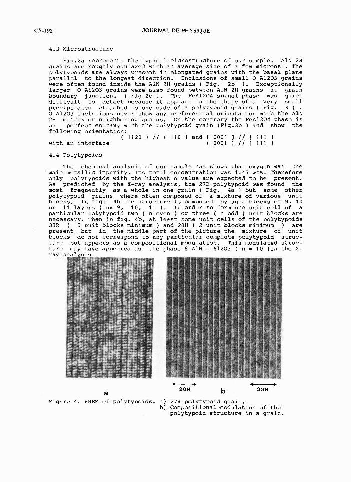
The chemical analysis of our sample has shown that oxygen was the main metallic impurity. Its total concentration was 1.43 wt%. Therefore only polytypoids with the highest n value are expected to be present. As predicted by the X-ray analysis, the 27R polytypoid was found the most frequently as a whole in one grain ( Fig. 4a ) but some other polytypoid grains where often composed of a mixture of various unit blocks. In fig. 4b the structure is composed by unit blocks of 9, 10 or 1 1 layers ( n= 9, 10, 1 1 ) . In order to form one unit cell of a particular polytypoid two ( n even ) or three ( n odd ) unit blocks are necessary. Then in fig. 4b, at least some unit cells of the polytypoids 33R ( 3 unit blocks minimum ) and 20H ( 2 unit blocks minimum ) are present but in the middle part of the picture the mixture of unit blocks do not correspond to any particular complete polytypoid struc- ture but appears as a compositional modulation. This modulated struc- ture may have appeared as the phase 8 A1N - A1203 ( n = 10 )in the X-
Figure 4. HREM of polytypoids. a) 27R polytypoid grain. b) Compositional -modulation of the
polytypoid structure in a grain.
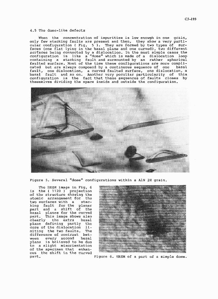
4.5 The dome-like defects
When the concentration of impurities is low enough in one grain, only few stacking faults are present and then, they show a very parti- cular configuration ( Fig. 5 ) . They are formed by two types of sur- faces (one flat lying in the basal plane and one curved), two different surfaces being connected by a dislocation. In the most simple cases the configuration is like a "dome" which is made of a dislocation loop containing a stacking fault and surmounted by an rather spherical faulted surface. Most of the time these configurations are more compli- cated but are always composed by a continuous sequence of one basal fault, one dislocation, a curved faulted surface, one dislocation, a basal fault and so on. Another very peculiar particularity of this configuration is the fact that these sequences of faults closes by themselves dividing the space inside and outside the configuration.
Figure 5. Several "dome" configurations within a A1N 2H grain.
The HREM image in Fig. 6 is the ( 1120 ) projection of the structure showing the atomic arrangement for the two surfaces with a stac- king fault for the planar part and a shift of the basal planes for the curved part. This image shows also clearly the extra basal plane defining partly the core of the dislocation li- miting the two faults. The difference of contrast bet- ween every second basal plane is believed to be due to a slight misorientation of the specimen that enhan- ces the shift in the curved part. Figure 6. HREM of a part of a simple dome.

C5-194 JOURNAL DE PHYSIQUE
The various displacement and Burgers vectors of these configura- tions have been determined by conventional TEM contrast experiments. There is for the basal plane a displacement of 1/6 [ 0001 ] in addition to the traditional stacking fault 1/3 [ 1100 ] ( Fig. 7a ). The curved surface is characterized by a 112 [ 0001 ] shift which is believed to give to the interface a very low energy configuration (Fig.7b ). The shape of the curved surface and its sometimes wavy aspect was a fair indication of a low energy configuration.
It is believed that the presence of oxygen impurities is the key point of the nucleation and growth of the dome configuration. A small number of non-metallic atoms filling the empty tetrahedral sites of the wurtzite structure induces the formation of a faulted dislocation loop. Inside the loop the structure is now energetically unstable and a shrinkage of the basal planes occurs in order to give the structure the opportunity to change its coordination from four to six. The actual difference of shift of the basal planes between this six atom coordinated structure inside the loop and the dislocation core of the same loop induces the nucleation of the dome surmounting the defect. The size of dome will increase by absorbing more oxygen atoms in the dislocation core of the loop. More complicated configurations are the result of the interaction of a growing dome with matrix dislocations or another defect within one grain. A more complete analysis of these configurations will appear soon in a separate publication .
Figure 7. Geometric description of the interfaces defining the dome: a) Basal part with an excess number of non-metal atoms. b) Curved part showing a low energy configuration.
REFERENCES
[I] K.H. JACK, J. Materials Science ( 1976 ) , 11, 1135. [2] D.P. THOMSON, P. KORGUL and A. HENDRY, in Nitrogen Ceramics ,
edited by F. L. RILEY ( 1983 ) , 61. [3] J.W. McCAWLEY and N. D. CORBIN, as above, 111. [4] G. VAN TENDELLOO, K.T. FABER and G. THOMAS, J. Materials Science
11983 ) , 18, 525. [5] K.M. KR.ISHNAN, R.S. RAI, G. THOMAS, N.D. CORBIN and J.M McCAWLEY,
Mat. Res. Soc. Symp. Proc. Vol. 60, 211. [ C ] Y-BANDO, M. MITOMO, Y. KITAMI and F. IZUMI, Journal of Microscopy
( 1986 142,235.