
HT66FU30
259
Enhanced A/D Flash Type MCU 8-Bit MCU with EEPROM HT66F20/HT66F30/HT66F40/HT66F50/HT66F60 HT66FU30/HT66FU40/HT66FU50/HT66FU60 Revision: 1.30 Date: October 4, 2010
Transcript of HT66FU30

Enhanced A/D Flash Type MCU 8-Bit MCU with EEPROM
HT66F20/HT66F30/HT66F40/HT66F50/HT66F60
HT66FU30/HT66FU40/HT66FU50/HT66FU60
Revision: 1.30 Date: October 4, 2010

Table of Contents
Technical Document ...........................................................................1
Features ...............................................................................................1CPU Features ........................................................................................................1
Peripheral Features................................................................................................1
General Description ............................................................................1
Selection Table ....................................................................................2
Block Diagram .....................................................................................2
Pin Assignment ...................................................................................3
Pin Description....................................................................................7HT66F20 ................................................................................................................7
HT66F30 ................................................................................................................8
HT66F40 ................................................................................................................9
HT66F50 ..............................................................................................................11
HT66F60 ..............................................................................................................12
Absolute Maximum Ratings .............................................................14
D.C. Characteristics ..........................................................................14
A.C. Characteristics ..........................................................................16
A/D Converter Characteristics .........................................................17
Comparator Electrical Characteristics ............................................18
Power-on Reset Characteristics ......................................................18
System Architecture .........................................................................19Clocking and Pipelining ........................................................................................19
Program Counter..................................................................................................20
Stack ....................................................................................................................20
Arithmetic and Logic Unit - ALU............................................................................20
Flash Program Memory ....................................................................21Structure...............................................................................................................21
Special Vectors.....................................................................................................21
Look-up Table.......................................................................................................21
Table Program Example .......................................................................................21
In Circuit Programming.........................................................................................22
RAM Data Memory.............................................................................23Structure...............................................................................................................23
Contents
i

Special Function Register Description ...........................................26
Indirect Addressing Registers - IAR0, IAR1....................................26Memory Pointers - MP0, MP1...............................................................................26
Bank Pointer - BP.................................................................................................27
Accumulator - ACC...............................................................................................28
Program Counter Low Register - PCL ..................................................................28
Look-up Table Registers - TBLP, TBHP, TBLH......................................................28
Status Register - STATUS ....................................................................................28
EEPROM Data Memory .....................................................................30EEPROM Data Memory Structure ........................................................................30
EEPROM Registers..............................................................................................30
Reading Data from the EEPROM .........................................................................32
Writing Data to the EEPROM ...............................................................................32
Write Protection....................................................................................................33
EEPROM Interrupt ...............................................................................................33
Programming Considerations ...............................................................................33
Oscillator............................................................................................34Oscillator Overview...............................................................................................34
System Clock Configurations................................................................................34
External Crystal/ Ceramic Oscillator - HXT ...........................................................35
External RC Oscillator - ERC................................................................................35
Internal RC Oscillator - HIRC................................................................................35
External 32.768kHz Crystal Oscillator - LXT .........................................................35
LXT Oscillator Low Power Function......................................................................36
Internal 32kHz Oscillator - LIRC ...........................................................................36
Supplementary Oscillators....................................................................................36
Operating Modes and System Clocks .............................................37System Clocks......................................................................................................37
System Operation Modes .....................................................................................38
Control Register ...................................................................................................39
Fast Wake-up .......................................................................................................40
Operating Mode Switching and Wake-up..............................................................41
NORMAL Mode to SLOW Mode Switching...........................................................41
SLOW Mode to NORMAL Mode Switching...........................................................42
Entering the SLEEP0 Mode..................................................................................42
Entering the SLEEP1 Mode..................................................................................43
Entering the IDLE0 Mode .....................................................................................43
Entering the IDLE1 Mode .....................................................................................43
Standby Current Considerations...........................................................................43
Wake-up...............................................................................................................44
Programming Considerations ...............................................................................44
Contents
ii

Watchdog Timer ................................................................................45Watchdog Timer Clock Source .............................................................................45
Watchdog Timer Control Register.........................................................................45
Watchdog Timer Operation...................................................................................46
Reset and Initialisation .....................................................................47Reset Functions ...................................................................................................47
Reset Initial Conditions.........................................................................................48
Input/Output Ports.............................................................................61Pull-high Resistors................................................................................................64
Port A Wake-up ....................................................................................................66
I/O Port Control Registers.....................................................................................66
Pin-remapping Functions......................................................................................69
Pin-remapping Registers ......................................................................................69
I/O Pin Structures .................................................................................................74
Programming Considerations ...............................................................................74
Timer Modules - TM...........................................................................76Introduction ..........................................................................................................76
TM Operation .......................................................................................................77
TM Clock Source..................................................................................................77
TM Interrupts........................................................................................................77
TM External Pins ..................................................................................................77
TM Input/Output Pin Control Registers .................................................................78
Programming Considerations ...............................................................................86
Compact Type TM..............................................................................87Compact TM Operation ........................................................................................87
Compact Type TM Register Description ...............................................................88
Compact Type TM Operating Modes ....................................................................91
Compare Match Output Mode ..............................................................................91
Timer/Counter Mode.............................................................................................91
PWM Output Mode...............................................................................................94
Standard Type TM - STM...................................................................96Standard TM Operation ........................................................................................96
Standard Type TM Register Description ...............................................................96
Standard Type TM Operating Modes..................................................................104
Compare Output Mode.......................................................................................104
Timer/Counter Mode...........................................................................................107
PWM Output Mode.............................................................................................107
Single Pulse Mode..............................................................................................110
Capture Input Mode ............................................................................................111
Contents
iii
Enhanced Type TM - ETM ...............................................................112Enhanced TM Operation.....................................................................................112
Enhanced Type TM Register Description............................................................113
Enhanced Type TM Operating Modes.................................................................118
Compare Output Mode .......................................................................................118
Timer/Counter Mode...........................................................................................123
PWM Output Mode.............................................................................................123
Single Pulse Output Mode..................................................................................128
Capture Input Mode............................................................................................130
Analog to Digital Converter............................................................132A/D Overview .....................................................................................................132
A/D Converter Register Description....................................................................132
A/D Converter Data Registers - ADRL, ADRH....................................................133
A/D Converter Control Registers - ADCR0, ADCR1, ACERL, ACERH ...............133
A/D Operation.....................................................................................................138
A/D Input Pins ....................................................................................................138
Summary of A/D Conversion Steps ....................................................................139
Programming Considerations .............................................................................140
A/D Transfer Function.........................................................................................140
A/D Programming Example ................................................................................140
Comparators ....................................................................................142Comparator Operation........................................................................................142
Comparator Registers ........................................................................................142
Comparator Interrupt ..........................................................................................142
Programming Considerations .............................................................................142
Serial Interface Module - SIM .........................................................145SPI Interface.......................................................................................................145
SPI Registers .....................................................................................................146
SPI Communication............................................................................................149
I2C Interface .......................................................................................................151
I2C Bus Communication......................................................................................155
I2C Bus Start Signal ............................................................................................155
Slave Address ....................................................................................................155
I2C Bus Read/Write Signal..................................................................................155
I2C Bus Slave Address Acknowledge Signal.......................................................155
I2C Bus Data and Acknowledge Signal ...............................................................156
Peripheral Clock Output .................................................................158Peripheral Clock Operation.................................................................................158
Contents
iv

Interrupts..........................................................................................159Interrupt Registers ..............................................................................................159
Interrupt Operation .............................................................................................171
External Interrupt ................................................................................................175
Comparator Interrupt ..........................................................................................175
Multi-function Interrupt ........................................................................................175
A/D Converter Interrupt.......................................................................................175
Time Base Interrupts ..........................................................................................175
Serial Interface Module Interrupt.........................................................................177
External Peripheral Interrupt ...............................................................................177
EEPROM Interrupt .............................................................................................177
LVD Interrupt ......................................................................................................177
TM Interrupts ......................................................................................................178
Interrupt Wake-up Function ................................................................................178
Programming Considerations .............................................................................178
Power Down Mode and Wake-up ...................................................179Entering the IDLE or SLEEP Mode.....................................................................179
Standby Current Considerations.........................................................................179
Wake-up.............................................................................................................179
Low Voltage Detector - LVD............................................................180LVD Register ......................................................................................................180
LVD Operation....................................................................................................181
SCOM Function for LCD .................................................................181LCD Operation ...................................................................................................181
LCD Bias Control................................................................................................181
Configuration Options ....................................................................184
Application Circuits ........................................................................185
UART Module Serial Interface ........................................................186UART Module Features......................................................................................186
UART Module Overview..................................................................186
UART Module Block Diagram.........................................................186
Pin Assignment ...............................................................................187
UART Module Pin Description .......................................................189
UART Module D.C. Characteristics................................................189
UART Module A.C. Characteristics................................................190
UART Module Functional Description...........................................191UART Module Internal Signal .............................................................................191
Contents
v

UART Module SPI Interface ............................................................191SPI Timing..........................................................................................................191
UART Module External Pin Interfacing..........................................192UART Data Transfer Scheme .............................................................................192
UART Commands ..............................................................................................193
UART Status and Control Registers ...................................................................193
Baud Rate Generator .........................................................................................198
UART Module Setup and Control...................................................200Managing Receiver Errors ..................................................................................203
UART Module Interrupt Structure ..................................................203
UART Module Power-down and Wake-up .....................................204
Using the UART Function...............................................................205
Application Circuit with UART Module..........................................206
Instruction Set .................................................................................207Introduction.........................................................................................................207
Instruction Timing ...............................................................................................207
Moving and Transferring Data ............................................................................207
Arithmetic Operations .........................................................................................207
Logical and Rotate Operations ...........................................................................207
Branches and Control Transfer...........................................................................207
Bit Operations.....................................................................................................208
Table Read Operations.......................................................................................208
Other Operations................................................................................................208
Instruction Set Summary ....................................................................................208
Instruction Definition ......................................................................210
Package Information.......................................................................22016-pin DIP (300mil) Outline Dimensions .............................................................220
16-pin NSOP (150mil) Outline Dimensions .........................................................223
16-pin SSOP (150mil) Outline Dimensions .........................................................224
20-pin DIP (300mil) Outline Dimensions .............................................................225
20-pin SOP (300mil) Outline Dimensions............................................................227
20-pin SSOP (150mil) Outline Dimensions .........................................................228
24-pin SKDIP (300mil) Outline Dimensions ........................................................229
24-pin SOP (300mil) Outline Dimensions............................................................232
24-pin SSOP (150mil) Outline Dimensions .........................................................233
28-pin SKDIP (300mil) Outline Dimensions ........................................................234
28-pin SOP (300mil) Outline Dimensions............................................................235
28-pin SSOP (150mil) Outline Dimensions .........................................................236
SAW Type 32-pin (5mm�5mm) QFN Outline Dimensions...................................237
SAW Type 40-pin (6mm�6mm for 0.75mm) QFN Outline Dimensions...............238
44-pin QFP (10mm�10mm) Outline Dimensions ................................................239
48-pin SSOP (300mil) Outline Dimensions .........................................................240
Contents
vi

SAW Type 48-pin (7mm�7mm) QFN Outline Dimensions...................................241
52-pin QFP (14mm�14mm) Outline Dimensions ................................................242
44-pin LQFP (10mm�10mm) (FP3.2mm) Outline Dimensions............................243
Product Tape and Reel Specifications ..........................................244Reel Dimensions ................................................................................................244
Carrier Tape Dimensions ....................................................................................246
Contents
vii

HT66F20/HT66F30/HT66F40/HT66F50/HT66F60
HT66FU30/HT66FU40/HT66FU50/HT66FU60
Enhanced A/D Flash Type MCU 8-Bit MCU with EEPROM
Rev. 1.30 1 October 4, 2010
General Description
The HT66FXX series of devices are Flash Memory A/D
type 8-bit high performance RISC architecture
microcontrollers. Offering users the convenience of Flash
Memory multi-programming features, these devices also
include a wide range of functions and features. Other
memory includes an area of RAM Data Memory as well as
an area of EEPROM memory for storage of non-volatile
data such as serial numbers, calibration data etc.
Analog features include a multi-channel 12-bit A/D con-
verter and dual comparator functions. Multiple and ex-
tremely flexible Timer Modules provide timing, pulse
generation and PWM generation functions. Communica-
tion with the outside world is catered for by including fully
integrated SPI or I2C interface functions, two popular inter-
faces which provide designers with a means of easy com-
munication with external peripheral hardware. Protective
features such as an internal Watchdog Timer, Low Voltage
Reset and Low Voltage Detector coupled with excellent
noise immunity and ESD protection ensure that reliable
operation is maintained in hostile electrical environments.
A full choice of HXT, LXT, ERC, HIRC and LIRC oscilla-
tor functions are provided including a fully integrated
system oscillator which requires no external compo-
nents for its implementation. The ability to operate and
switch dynamically between a range of operating
modes using different clock sources gives users the
ability to optimise microcontroller operation and mini-
mise power consumption.
The UART module is contained in the HT66FUx0 series of
devices. It can support the applications such as data com-
munication networks between microcontrollers, low-cost
data links between PCs and peripheral devices, portable
and battery operated device communication, etc.
The inclusion of flexible I/O programming features,
Time-Base functions along with many other features en-
sure that the devices will find excellent use in applica-
tions such as electronic metering, environmental
monitoring, handheld instruments, household appli-
ances, electronically controlled tools, motor driving in
addition to many others.
Features
CPU Features
� Operating Voltage:
fSYS= 8MHz: 2.2V~5.5V
fSYS= 12MHz: 2.7V~5.5V
fSYS= 20MHz: 4.5V~5.5V
� Up to 0.2�s instruction cycle with 20MHz system
clock at VDD=5V� Power down and wake-up functions to reduce power
consumption� Five oscillators:
External Crystal -- HXT
External 32.768kHz Crystal -- LXT
External RC -- ERC
Internal RC -- HIRC
Internal 32kHz RC -- LIRC� Multi-mode operation: NORMAL, SLOW, IDLE and
SLEEP� Fully integrated internal 4MHz, 8MHz and 12MHz
oscillator requires no external components� All instructions executed in one or two instruction
cycles� Table read instructions� 63 powerful instructions� Up to 12-level subroutine nesting� Bit manipulation instruction
Peripheral Features
� Flash Program Memory: 1K�14 ~ 12K�16
� RAM Data Memory: 64�8 ~ 576�8
� EEPROM Memory: 32�8~256�8
� Watchdog Timer function
� Up to 50 bidirectional I/O lines
� Software controlled 4-SCOM lines LCD driver with
1/2 bias
� Multiple pin-shared external interrupts
� Multiple Timer Module for time measure, input
capture, compare match output, PWM output or
single pulse output function
� Serial Interfaces Module -- SIM for SPI or I2C
� Dual Comparator functions
� Dual Time-Base functions for generation of fixed time
interrupt signals
� Multi-channel 12-bit resolution A/D converter
� Low voltage reset function
� Low voltage detect function
� Optional peripheral -- UART module for fully duplex
asynchronous communication
� Wide range of available package types
Technical Document
� Application Note� HA0075E MCU Reset and Oscillator Circuits Application Note

Selection Table
Most features are common to all devices, the main feature distinguishing them are Memory capacity, I/O count, TM
features, stack capacity and package types. The following table summarises the main features of each device.
Part No. VDDProgram
Memory
Data
Memory
Data
EEPROMI/O
Ext.
Int.A/D
Timer
Module
Interface
(SPI/I2C)
UART Stack Package
HT66F202.2V~
5.5V1K�14 64�8 32�8 18 2 12-bit�8
10-bit CTM�1,
10-bit STM�1� � 4
16DIP/NSOP/SSOP
20DIP/SOP/SSOP
HT66F30 2.2V~
5.5V2K�14 96�8 64�8
22
2 12-bit�810-bit CTM�1,
10-bit ETM�1�
�4
16DIP/NSOP/SSOP
20DIP/SOP/SSOP
24SKDIP/SOP/SSOP
HT66FU30 14 � 24SKDIP/SOP
HT66F402.2V~
5.5V4K�15 192�8 128�8
42
2 12-bit�8
10-bit CTM�1,
10-bit ETM�1,
16-bit STM�1
�
�
8
24/28SKDIP/SOP/SSOP
44LQFP
32/40QFN, 48SSOP/QFN
HT66FU40 34 �40QFN, 44LQFP,
48SSOP/QFN
HT66F50 2.2V~
5.5V8K�16 384�8 256�8
42
2 12-bit�8
10-bit CTM�2,
10-bit ETM�1,
16-bit STM�1
��
8
28SKDIP/SOP/SSOP
44LQFP, 40QFN
48SSOP/QFN
HT66FU50 34 � 44LQFP, 48QFN
HT66F602.2V~
5.5V12K�16 576�8 256�8
50
4 12-bit�12
10-bit CTMx2,
10-bit ETMx1,
16-bit STMx1
�
�
12
52QFP, 40QFN, 44LQFP
48SSOP/LQFP/QFN
HT66FU60 42 �52QFP, 40QFN, 44LQFP
48LQFP/QFN
Note: As devices exist in more than one package format, the table reflects the situation for the package with the most
pins.
There is an additional peripheral known as the UART module in HT66FU30, HT66FU40, HT66FU50 and
HT66FU60 devices. All information related to the UART Module will be described in the following UART Mod-
ule section.
Block Diagram
HT66F20/HT66F30/HT66F40/HT66F50/HT66F60HT66FU30/HT66FU40/HT66FU50/HT66FU60
Rev. 1.30 2 October 4, 2010
� � � � � � � � � � � � � � � � � �� � � � � � � � � � � �
� � � � � � � �� � �
! " # � � � � �� � $� �
� �� � � � � �
� � � � % �� � � � � � �
� � � & ' �� � � � � � � � �
( ) " * � � � + � ,� � � - �
. � � � . ' �� � � � � � � � �
& � �� � � � � � � � �
� � � � /
� � � �, � � �
� � � �
� � � � � � � � �� � � �
+ �, � � �
� � � �
$ + � � � � � � 0
. � 12 � � � � � � �
. � 12 � � � � � , � � �
� � ( � � �
� � � % � � � � �
� * 0 � � * (
� � �

Pin Assignment
Note: 1. Bracketed pin names indicate non-default pinout remapping locations.
2. If the pin-shared pin functions have multiple outputs simultaneously, its pin names at the right side of the
�/� sign can be used for higher priority.
3. VDD&AVDD means the VDD and AVDD are the double bonding.
HT66F20/HT66F30/HT66F40/HT66F50/HT66F60HT66FU30/HT66FU40/HT66FU50/HT66FU60
Rev. 1.30 3 October 4, 2010
� � � � � � �
� � � � � � � � � � � � � � � � �
( 3
( 4
( 5
( 6
( )
( (
( 0
7
(
)
6
5
4
3
8
!
+ ( � � ( 9 0 � + : (
+ ) � � � ; 0 � � 0 < � + : )
+ 6 � � : � 0 � � 0 " � + : 6
+ 5 � � : � ( � � � ; ( � + : 5
+ 4 � � ( ' � � , � � + : 4
+ 3 � � , � � � , + � + : 3
+ 8 � � � ; � � � . � + : 8
* 4 � � � � � 2 � �
+ 0 � � 0 ' � � 0 9 0 � + : 0
2 � � = + 2 � �
* 5 � ' � )
* 6 � ' � (
* ) � � � � )
* ( � � � � (
2 , , = + 2 , ,
* 0 � � �
) 0
( 7
( !
( 8
( 3
( 4
( 5
( 6
( )
( (
(
)
6
5
4
3
8
!
7
( 0
+ ( � � ( 9 0 � + : (
+ ) � � � ; 0 � � 0 < � + : )
+ 6 � � : � 0 � � 0 " � + : 6
+ 5 � � : � ( � � � ; ( � + : 5
+ 4 � � ( ' � � , � � + : 4
+ 3 � � , � � � , + � + : 3
+ 8 � � � ; � � � . � + : 8
* 4 � � � � � 2 � �
� ) � � ; � � ( < � � � � � )
� 6 � � : � � � ( " � � � � � 6
+ 0 � � 0 ' � � 0 9 0 � + : 0
2 � � = + 2 � �
* 5 � ' � )
* 6 � ' � (
* ) � � � � )
* ( � � � � (
2 , , = + 2 , ,
* 0 � � �
� ( � � � � � (
� 0 � � ( 9 ( � � � � � 0
� � � � � � �
� � � � � � � � � � � � � � � �
� � � � � � �
� � � � � � � � � � � � � � � � �
( 3
( 4
( 5
( 6
( )
( (
( 0
7
(
)
6
5
4
3
8
!
+ ( � � ( + � + : (
+ ) � � � ; 0 � � 0 < � + : )
+ 6 � � : � 0 � � 0 " � + : 6
+ 5 � � : � ( � � � ; ( � + : 5
+ 4 � � ( ' � � , � � + : 4
+ 3 � � , � � � , + � + : 3
+ 8 � � � ; � � � . � + : 8
* 4 � � � � � 2 � �
+ 0 � � 0 ' � � 0 9 0 � + : 0
2 � � = + 2 � �
* 5 � ' � )
* 6 � ' � (
* ) � � � � )
* ( � � � � (
2 , , = + 2 , ,
* 0 � � �
) 0
( 7
( !
( 8
( 3
( 4
( 5
( 6
( )
( (
(
)
6
5
4
3
8
!
7
( 0
+ ( � � ( + � + : (
+ ) � � � ; 0 � � 0 < � + : )
+ 6 � � : � 0 � � 0 " � + : 6
+ 5 � � : � ( � � � ; ( � + : 5
+ 4 � � ( ' � � , � � + : 4
+ 3 � � , � � � , + � + : 3
+ 8 � � � ; � � � . � + : 8
* 4 � � � � � 2 � �
� ) � � ; � � ( <
� 6 � � : � � � ( "
+ 0 � � 0 ' � � 0 9 0 � + : 0
2 � � = + 2 � �
* 5 � ' � )
* 6 � ' � (
* ) � � � � )
* ( � � � � (
2 , , = + 2 , ,
* 0 � � �
� ( � � ( * 9 ( � > � , � ? � � � � � (
� 0 � � ( * 9 0 � > � , � � � , + ? � � � � � 0
� � � � � � �
� � � � � � � � � � � � � � � �
) 5
) 6
) )
) (
) 0
( 7
( !
( 8
( 3
( 4
( 5
( 6
(
)
6
5
4
3
8
!
7
( 0
( (
( )
� � � � � � �
� � � � � � � � � � � � � � � � � �
+ 0 � � 0 ' � � 0 9 0 � + : 0
2 � � = + 2 � �
* 5 � ' � )
* 6 � ' � (
* ) � � � � )
* ( � � � � (
2 , , = + 2 , ,
* 0 � � �
� ( � � ( * 9 ( � > � , � ? � � � � � (
� 0 � � ( * 9 0 � > � , � � � , + ? � � � � � 0
� 8 � > � � ; � � � . ? � � � � � 6
� 3 � > � � � ? � � � � � )
+ ( � � ( + � + : (
+ ) � � � ; 0 � � 0 < � + : )
+ 6 � � : � 0 � � 0 " � + : 6
+ 5 � � : � ( � � � ; ( � + : 5
+ 4 � � ( ' � � , � � + : 4
+ 3 � � , � � � , + � + : 3
+ 8 � � � ; � � � . � + : 8
* 4 � � � � � 2 � �
� ) � � ; � � ( <
� 6 � � : � � � ( "
� 5 � > � : � ?
� 4 � � 0 9 ( � > � ; ?
+ ( � � ( + � + : (
+ ) � � � ; 0 � � 0 < � + : )
+ 6 � � : � 0 � � 0 " � + : 6
+ 5 � � : � ( � � � ; ( � + : 5
+ 4 � � ( ' � � , � � + : 4
+ 3 � � , � � � , + � + : 3
+ 8 � � � ; � � � . � + : 8
* 4 � � � � � 2 � �
� ) � � � ; ) � � ; � � ( <
� 6 � � : � � � ) 9 0 � � ( "
� 5 � > � : � 0 ? � > � : � ? � � ) 9 (
� 4 � > � : � ( ? � � 0 9 ( � � ( * 9 ) � > � ; ?
, 0 � > � � ; ) ? � > � � � ?
, ( � > � ) 9 0 ? � > � , � ? � > � � ; � � � . ?
) !
) 8
) 3
) 4
) 5
) 6
) )
) (
) 0
( 7
( !
( 8
( 3
( 4
(
)
6
5
4
3
8
!
7
( 0
( (
( )
( 6
( 5
� � � � � � �
� � � � � � � � � � � � � � � � � �
+ 0 � � 0 ' � � 0 9 0 � + : 0
2 � � = + 2 � �
* 5 � ' � )
* 6 � ' � (
* ) � � � � )
* ( � � � � (
2 , , = + 2 , ,
* 0 � � �
� ( � � ( * 9 ( � � � � � (
� 0 � � ( * 9 0 � � � � � 0
� 8 � > � ( + ? � � � � � 6
� 3 � > � 0 9 0 ? � � � � � )
, 6 � > � � ; ( ? � > � , � ?
, ) � > � � ; 0 ? � > � , � � � , + ?
� � � � � � �
� � � � � � � � � � � � � � � � � �
) 5
) 6
) )
) (
) 0
( 7
( !
( 8
( 3
( 4
( 5
( 6
(
)
6
5
4
3
8
!
7
( 0
( (
( )
+ 0 � � 0 ' � � 0 9 0 � + : 0
2 � � = + 2 � �
* 5 � ' � )
* 6 � ' � (
* ) � � � � )
* ( � � � � (
2 , , = + 2 , ,
* 0 � � �
� ( � � ( * 9 ( � � � � � (
� 0 � � ( * 9 0 � � � � � 0
� 8 � > � ( + ? � � � � � 6
� 3 � > � 0 9 0 ? � � � � � )
+ ( � � ( + � + : (
+ ) � � � ; 0 � � 0 < � + : )
+ 6 � � : � 0 � � 0 " � + : 6
+ 5 � � : � ( � � � ; ( � + : 5
+ 4 � � ( ' � � , � � + : 4
+ 3 � � , � � � , + � + : 3
+ 8 � � � ; � � � . � + : 8
* 4 � � � � � 2 � �
� ) � � � ; ) � � ; � � ( <
� 6 � � : � � � ) 9 0 � � ( "
� 5 � > � : � 0 ? � > � : � ? � � ) 9 (
� 4 � > � : � ( ? � � 0 9 ( � � ( * 9 ) � > � ; ?

Note: 1. Bracketed pin names indicate non-default pinout remapping locations.
2. If the pin-shared pin functions have multiple outputs simultaneously, its pin names at the right side of the
�/� sign can be used for higher priority.
3. VDD&AVDD means the VDD and AVDD are the double bonding.
HT66F20/HT66F30/HT66F40/HT66F50/HT66F60HT66FU30/HT66FU40/HT66FU50/HT66FU60
Rev. 1.30 4 October 4, 2010
� � � � � � �
� � � � � �
( 6 ( 5 ( 4 ( 3 ( 8 ( ! ( 7 ) 0 ) ( ) ) ) 6 ) 5
(
)
6
5
4
3
8
!
7
( 0
( (
( )
6 3
6 4
6 5
6 6
6 )
6 (
6 0
) 7
) !
) 8
) 3
) 4
6 86 !6 75 05 (5 )5 65 55 45 35 85 !: �
* 4 � � � � � 2 � �
+ 8 � � � ; � � � . � + : 8
+ 3 � � , � � � , + � + : 3
+ 4 � � ( ' � � , � � + : 4
+ 5 � � : � ( � � � ; ( � + : 5
+ 6 � � : � 0 � � 0 " � + : 6
+ ) � � � ; 0 � � 0 < � + : )
+ ( � � ( + � + : (
+ 0 � � 0 ' � � 0 9 0 � + : 0
: �
� ( � > � ( ' ?
,)�>�
�;0?�>�
,���
,+?
,(�>�
)90?�>�
,�?�>�
�;���.?
,0�>�
�;)?�>�
��?
:�
�4�>�:
�(?��
09(��(*9)�>
�;?
�5�>�:
�0?�>
�:�?��
)9(
�6��:���)90��("
�)���;)��;��(<
,8�>�
��?
,3�>�
�;���.?
*8�>�
,���
,+?
*3�>�
,�?
, 6 � > � � ; ( ? � > � , � ?
, 5 � > � ) 9 ( ?
, 4 � > � 0 9 ( ?
� 0
� (
� )
� 6
� 3 � > � 0 9 0 ? � � � � � )
� 8 � > � ( + ? � � � � � 6
: �
� 0 � � ( * 9 0 � � � � � 0
� ( � � ( * 9 ( � � � � � (
�5�>�
(*9)?
�4
*0���
2,,=+2,,
*(��
��(
*)��
��)
*6�'�(
*5�'�)
2��=+2��
�3�>�:
�0?
�8�>�:
�(?
�0�>�
0'?
� � � � � � �
� � � � � � �
(
)
6
5
4
3
8
!
7
( 0
( (( ) ( 6 ( 5 ( 4 ( 3 ( 8 ( ! ( 7 ) 0 ) ( ) )
) 6
) 5
) 4
) 3
) 8
) !
) 7
6 0
6 (
6 )
6 66 56 46 36 86 !6 75 05 (5 )5 65 5
* 4 � � � � � 2 � �
+ 8 � � � ; � � � . � + : 8
+ 3 � � , � � � , + � + : 3
+ 4 � � ( ' � � , � � + : 4
+ 5 � � : � ( � � � ; ( � + : 5
+ 6 � � : � 0 � � 0 " � + : 6
+ ) � � � ; 0 � � 0 < � + : )
+ ( � � ( + � + : (
+ 0 � � 0 ' � � 0 9 0 � + : 0
� ( � > � ( ' ?
� 0 � > � 0 ' ?
, 6 � > � � ; ( ? � > � , � ?
, 5 � > � ) 9 ( ?
, 4 � > � 0 9 ( ?
� 0
� (
� )
� 6
� 3 � > � 0 9 0 ? � � � � � )
� 8 � > � ( + ? � � � � � 6
� 0 � � ( * 9 0 � � � � � 0
� ( � � ( * 9 ( � � � � � (
,)�>�
�;0?�>�
,���
,+?
,(�>�
)90?�>�
,�?�>�
�;���.?
,0�>�
�;)?�>�
��?
�4�>�:
�(?��
09(��(*9)�>
�;?
�5�>�:
�0?�>
�:�?��
)9(
�6��:���)90��("
�)���;)��;��(<
,8�>�
��?
,3�>�
�;���.?
*8�>�
,���
,+?
*3�>�
,�?
�5�>�
(*9)?
�4
*0���
2,,=+2,,
*(��
��(
*)��
��)
*6�'�(
*5�'�)
2��=+2��
�3�>�:
�0?
�8�>�:
�(?
� � � � � � �
� � � � � �
(
)
6
5
4
3
8
!7 ( 0 ( ( ( ) ( 6 ( 5 ( 4 ( 3
( 8
( !
( 7
) 0
) (
) )
) 6
) 5) 4) 3) 8) !) 76 06 (6 )
+ 5 � � : � ( � � � ; ( � + : 5
+ 6 � � : � 0 � � 0 " � + : 6
+ ) � � � ; 0 � � 0 < � + : )
+ ( � � ( + � + : (
+ 0 � � 0 ' � � 0 9 0 � + : 0
� ( � > � ( ' ?
� 0 � > � 0 ' ?
� 8 � > � : � ( ?
, 0 � > � � ; ) ? � > � � � ?
, ( � > � ) 9 0 ? � > � , � ? � > � � ; � � � . ?
, ) � > � � ; 0 ? � > � , � � � , + ?
, 6 � > � � ; ( ? � > � , � ?
� 3 � > � 0 9 0 ? � � � � � )
� 8 � > � ( + ? � � � � � 6
� 0 � � ( * 9 0 � � � � � 0
� ( � � ( * 9 ( � � � � � (
*0���
2,,=+2,,
*(��
��(
*)��
��)
*6�'�(
*5�'�)
2��=+2��
�3�>�:
�0?
�4�>�:
�(?��
09(��(*9)�>
�;?
�5�>�:
�0?�>
�:�?��
)9(
�6��:���)90��("
�)���;)��;��(<
*4�����2��
+8���;���.�+:8
+3��,���
,+�+:3
+4��('��,��+:4
� � � � � � �
� � � � � �
(
)
6
5
4
3
8
!
7
( 0( ( ( ) ( 6 ( 5 ( 4 ( 3 ( 8 ( ! ( 7 ) 0
) (
) )
) 6
) 5
) 4
) 3
) 8
) !
) 7
6 06 (6 )6 66 56 46 36 86 !6 75 0
* 4 � � � � � 2 � �
+ 8 � � � ; � � � . � + : 8
+ 3 � � , � � � , + � + : 3
+ 4 � � ( ' � � , � � + : 4
+ 5 � � : � ( � � � ; ( � + : 5
+ 6 � � : � 0 � � 0 " � + : 6
+ ) � � � ; 0 � � 0 < � + : )
+ ( � � ( + � + : (
+ 0 � � 0 ' � � 0 9 0 � + : 0
� ( � > � ( ' ?
*0���
2,,=+2,,
*(��
��(
*)��
��)
*6�'�(
*5�'�)
2��=+2��
�3�>�:
�0?
�8�>�:
�(?
�0�>�
0'?
,(�>�
)90?�>�
,�?�>�
�;���.?
,0�>�
�;)?�>�
��?
�4�>�:
�(?��
09(��(*9)�>
�;?
�5�>�:
�0?�>
�:�?��
)9(
�6��:���)90��("
�)���;)��;��(<
,8�>�
��?
,3�>�
�;���.?
*8�>�
,���
,+?
*3�>�
,�?
, ) � > � � ; 0 ? � > � , � � � , + ?
, 6 � > � � ; ( ? � > � , � ?
, 5 � > � ) 9 ( ?
, 4 � > � 0 9 ( ?
� 3 � > � 0 9 0 ? � � � � � )
� 8 � > � ( + ? � � � � � 6
� 0 � � ( * 9 0 � � � � � 0
� ( � � ( * 9 ( � � � � � (
� 5 � > � ( * 9 ) ?
� 4
+ ( � � ( + � + : (
+ ) � � � ; 0 � � 0 < � + : )
+ 6 � � : � 0 � � 0 " � + : 6
+ 5 � � : � ( � � � ; ( � + : 5
+ 4 � � ( ' � � , � � + : 4
+ 3 � � , � � � , + � + : 3
+ 8 � � � ; � � � . � + : 8
* 4 � � � � � 2 � �
* 3 � > � , � ?
* 8 � > � , � � � , + ?
, 3 � > � � ; � � � . ?
, 8 � > � � � ?
� 5 � > � : � 0 ? � > � : � ? � � ) 9 (
: �
: �
: �
� ) � � � ; ) � � ; � � ( <
� 6 � � : � � � ) 9 0 � � ( "
� 4 � > � : � ( ? � � 0 9 ( � � ( * 9 ) � > � ; ?
, 0 � > � � ; ) ? � > � � � ?
, ( � > � ) 9 0 ? � > � , � ? � > � � ; � � � . ?
, ) � > � � ; 0 ? � > � , � � � , + ?
, 6 � > � � ; ( ? � > � , � ?
, 5 � > � ) 9 ( ?
5 !
5 8
5 3
5 4
5 5
5 6
5 )
5 (
5 0
6 7
6 !
6 8
6 3
6 4
6 5
6 6
6 )
6 (
6 0
) 7
) !
) 8
) 3
) 4
(
)
6
5
4
3
8
!
7
( 0
( (
( )
( 6
( 5
( 4
( 3
( 8
( !
( 7
) 0
) (
) )
) 6
) 5
+ 0 � � 0 ' � � 0 9 0 � + : 0
� ( � > � ( ' ?
� 0 � > � 0 ' ?
� 8 � > � : � ( ?
� 3 � > � : � 0 ?
2 � � = + 2 � �
* 5 � ' � )
* 6 � ' � (
* ) � � � � )
* ( � � � � (
2 , , = + 2 , ,
* 0 � � �
� 4
� 5 � > � ( * 9 ) ?
� ( � � ( * 9 ( � � � � � (
� 0 � � ( * 9 0 � � � � � 0
: �
� 8 � > � ( + ? � � � � � 6
� 3 � > � 0 9 0 ? � � � � � )
� 6
� )
� (
� 0
, 4 � > � 0 9 ( ?
� � � � � � �
� � � � � � �

Note: 1. Bracketed pin names indicate non-default pinout remapping locations.
2. If the pin-shared pin functions have multiple outputs simultaneously, its pin names at the right side of the
�/� sign can be used for higher priority.
3. VDD&AVDD means the VDD and AVDD are the double bonding.
HT66F20/HT66F30/HT66F40/HT66F50/HT66F60HT66FU30/HT66FU40/HT66FU50/HT66FU60
Rev. 1.30 5 October 4, 2010
� � � � � � �
� � � � � �
( 6 ( 5 ( 4 ( 3 ( 8 ( ! ( 7 ) 0 ) ( ) ) ) 6 ) 5
(
)
6
5
4
3
8
!
7
( 0
( (
( )
6 3
6 4
6 5
6 6
6 )
6 (
6 0
) 7
) !
) 8
) 3
) 4
6 86 !6 75 05 (5 )5 65 55 45 35 85 !: �
* 4 � � � � � 2 � �
+ 8 � � � ; � � � . � + : 8
+ 3 � � , � � � , + � + : 3
+ 4 � � ( ' � � , � � + : 4
+ 5 � � : � ( � � � ; ( � + : 5
+ 6 � � : � 0 � � 0 " � + : 6
+ ) � � � ; 0 � � 0 < � + : )
+ ( � � ( + � + : (
+ 0 � � 0 ' � � 0 9 0 � + : 0
: �
� ( � > � ( ' ?
,)�>�
�;0?�>�
,���
,+?
,(�>�
)90?�>�
,�?�>�
�;���.?
,0�>�
�;)?��
69(�>�
��?
:�
�4�>�:
�(?��
09(��(*9)�>
�;?
�5�>�:
�0?�>
�:�?��
�;6��)9(
�6��:
���)90��
("
�)���;)��;��
(<
,8�>�
��?
,3�>�
�;���.?
*8�>�
,���
,+?
*3�>�
,�?
, 6 � > � � ; ( ? � � 6 9 0 � > � , � ?
, 5 � > � ) 9 ( ?
, 4 � > � 0 9 ( ?
� 0
� (
� )
� 6 � > � 6 9 ( ?
� 3 � > � 0 9 0 ? � � � � � )
� 8 � > � ( + ? � � � � � 6
: �
� 0 � � ( * 9 0 � � � � � 0
� ( � � ( * 9 ( � � � � � (
�5�>�
(*9)?
�4�>�
690?
*0�
��
2,,=+2,,
*(��
��(
*)��
��)
*6�'�(
*5�'�)
2��=+2��
�3�>�:
�0?
�8�>�:
�(?
�0�>�
0'?
� � � � � � �
� � � � � � �
(
)
6
5
4
3
8
!
7
( 0
( (( ) ( 6 ( 5 ( 4 ( 3 ( 8 ( ! ( 7 ) 0 ) ( ) )
) 6
) 5
) 4
) 3
) 8
) !
) 7
6 0
6 (
6 )
6 66 56 46 36 86 !6 75 05 (5 )5 65 5
* 4 � � � � � 2 � �
+ 8 � � � ; � � � . � + : 8
+ 3 � � , � � � , + � + : 3
+ 4 � � ( ' � � , � � + : 4
+ 5 � � : � ( � � � ; ( � + : 5
+ 6 � � : � 0 � � 0 " � + : 6
+ ) � � � ; 0 � � 0 < � + : )
+ ( � � ( + � + : (
+ 0 � � 0 ' � � 0 9 0 � + : 0
� ( � > � ( ' ?
� 0 � > � 0 ' ?
, 6 � > � � ; ( ? � � 6 9 0 � > � , � ?
, 5 � > � ) 9 ( ?
, 4 � > � 0 9 ( ?
� 0
� (
� )
� 6 � > � 6 9 ( ?
� 3 � > � 0 9 0 ? � � � � � )
� 8 � > � ( + ? � � � � � 6
� 0 � � ( * 9 0 � � � � � 0
� ( � � ( * 9 ( � � � � � (
�5�>�
(*9)?
�4�>�
690?
*0�
��
2,,=+2,,
*(��
��(
*)��
��)
*6�'�(
*5�'�)
2��=+2��
�3�>�:
�0?
�8�>�:
�(?
,)�>�
�;0?�>�
,���
,+?
,(�>�
)90?�>�
,�?�>�
�;���.?
,0�>�
�;)?��
69(�>�
��?
�4�>�:
�(?��
09(��(*9)�>
�;?
�5�>�:
�0?�>
�:�?��
�;6��)9(
�6��:
���)90��
("
�)���;)��;��
(<
,8�>�
��?
,3�>�
�;���.?
*8�>�
,���
,+?
*3�>�
,�?
) !
) 8
) 3
) 4
) 5
) 6
) )
) (
) 0
( 7
( !
( 8
( 3
( 4
(
)
6
5
4
3
8
!
7
( 0
( (
( )
( 6
( 5
+ 0 � � 0 ' � � 0 9 0 � + : 0
2 � � = + 2 � �
* 5 � ' � )
* 6 � ' � (
* ) � � � � )
* ( � � � � (
2 , ,
* 0 � � �
� ( � � ( * 9 ( � � � � � (
� 0 � � ( * 9 0 � � � � � 0
� 8 � > � ( + ? � � � � � 6
� 3 � > � 0 9 0 ? � � � � � )
, 6 � > � � ; ( ? � � 6 9 0 � > � , � ?
, ) � > � � ; 0 ? � > � , � � � , + ?
+ ( � � ( + � + : (
+ ) � � � ; 0 � � 0 < � + : )
+ 6 � � : � 0 � � 0 " � + : 6
+ 5 � � : � ( � � � ; ( � + : 5
+ 4 � � ( ' � � , � � + : 4
+ 3 � � , � � � , + � + : 3
+ 8 � � � ; � � � . � + : 8
* 4 � � � � � 2 � �
� ) � � � ; ) � � ; � � ( <
� 6 � � : � � � ) 9 0 � � ( "
� 5 � > � : � 0 ? � > � : � ? � � � ; 6 � � ) 9 (
� 4 � > � : � ( ? � � 0 9 ( � � ( * 9 ) � > � ; ?
, 0 � > � � ; ) ? � � 6 9 ( � > � � � ?
, ( � > � ) 9 0 ? � > � , � ? � > � � ; � � � . ?
� � � � � � �
� � � � � � � � � � � � � � � � � �
� � � � � � �
� � � � � �
(
)
6
5
4
3
8
!
7
( 0( ( ( ) ( 6 ( 5 ( 4 ( 3 ( 8 ( ! ( 7 ) 0
) (
) )
) 6
) 5
) 4
) 3
) 8
) !
) 7
6 06 (6 )6 66 56 46 36 86 !6 75 0
* 4 � � � � � 2 � �
+ 8 � � � ; � � � . � + : 8
+ 3 � � , � � � , + � + : 3
+ 4 � � ( ' � � , � � + : 4
+ 5 � � : � ( � � � ; ( � + : 5
+ 6 � � : � 0 � � 0 " � + : 6
+ ) � � � ; 0 � � 0 < � + : )
+ ( � � ( + � + : (
+ 0 � � 0 ' � � 0 9 0 � + : 0
� ( � > � ( ' ?
*0�
��
2,,=+2,,
*(��
��(
*)��
��)
*6�'�(
*5�'�)
2��=+2��
�3�>�:
�0?
�8�>�:
�(?
�0�>�
0'?
,(�>�
)90?�>�
,�?�>�
�;���.?
,0�>�
�;)?��
69(�>�
��?
�4�>�:
�(?��
09(��(*9)�>
�;?
�5�>�:
�0?�>
�:�?��
�;6��)9(
�6��:
���)90��
("
�)���;)��;��
(<
,8�>�
��?
,3�>�
�;���.?
*8�>�
,���
,+?
*3�>�
,�?
, ) � > � � ; 0 ? � > � , � � � , + ?
, 6 � > � � ; ( ? � � 6 9 0 � > � , � ?
, 5 � > � ) 9 ( ?
, 4 � > � 0 9 ( ?
� 3 � > � 0 9 0 ? � � � � � )
� 8 � > � ( + ? � � � � � 6
� 0 � � ( * 9 0 � � � � � 0
� ( � � ( * 9 ( � � � � � (
� 5 � > � ( * 9 ) ?
� 4 � > � 6 9 0 ?
+ ( � � ( + � + : (
+ ) � � � ; 0 � � 0 < � + : )
+ 6 � � : � 0 � � 0 " � + : 6
+ 5 � � : � ( � � � ; ( � + : 5
+ 4 � � ( ' � � , � � + : 4
+ 3 � � , � � � , + � + : 3
+ 8 � � � ; � � � . � + : 8
* 4 � � � � � 2 � �
* 3 � > � , � ?
* 8 � > � , � � � , + ?
, 3 � > � � ; � � � . ?
, 8 � > � � � ?
� 5 � > � : � 0 ? � > � : � ? � � ) 9 (
: �
: �
: �
� ) � � � ; ) � � ; � � ( <
� 6 � � : � � � ) 9 0 � � ( "
� 4 � > � : � ( ? � � 0 9 ( � � ( * 9 ) � > � ; ?
, 0 � > � � ; ) ? � > � � � ?
, ( � > � ) 9 0 ? � > � , � ? � > � � ; � � � . ?
, ) � > � � ; 0 ? � > � , � � � , + ?
, 6 � > � � ; ( ? � > � , � ?
, 5 � > � ) 9 ( ?
5 !
5 8
5 3
5 4
5 5
5 6
5 )
5 (
5 0
6 7
6 !
6 8
6 3
6 4
6 5
6 6
6 )
6 (
6 0
) 7
) !
) 8
) 3
) 4
(
)
6
5
4
3
8
!
7
( 0
( (
( )
( 6
( 5
( 4
( 3
( 8
( !
( 7
) 0
) (
) )
) 6
) 5
+ 0 � � 0 ' � � 0 9 0 � + : 0
� ( � > � ( ' ?
� 0 � > � 0 ' ?
� 8 � > � : � ( ?
� 3 � > � : � 0 ?
2 � � = + 2 � �
* 5 � ' � )
* 6 � ' � (
* ) � � � � )
* ( � � � � (
2 , , = + 2 , ,
* 0 � � �
� 4 � > � 6 9 0 ?
� 5 � > � ( * 9 ) ?
� ( � � ( * 9 ( � � � � � (
� 0 � � ( * 9 0 � � � � � 0
: �
� 8 � > � ( + ? � � � � � 6
� 3 � > � 0 9 0 ? � � � � � )
� 6 � > � 6 9 ( ?
� )
� (
� 0
, 4 � > � 0 9 ( ?
� � � � � � �
� � � � � � �

Note: 1. Bracketed pin names indicate non-default pinout remapping locations.
2. If the pin-shared pin functions have multiple outputs simultaneously, its pin names at the right side of the
�/� sign can be used for higher priority.
3. VDD&AVDD means the VDD and AVDD are the double bonding.
HT66F20/HT66F30/HT66F40/HT66F50/HT66F60HT66FU30/HT66FU40/HT66FU50/HT66FU60
Rev. 1.30 6 October 4, 2010
� � � � � � �� � � � � � � � � � � �
( 6 ( 5 ( 4 ( 3 ( 8 ( ! ( 7 ) 0 ) ( ) ) ) 6 ) 5
(
)
6
5
4
3
8
!
7
( 0
( (
( )
6 3
6 4
6 5
6 6
6 )
6 (
6 0
) 7
) !
) 8
) 3
) 4
6 86 !6 75 05 (5 )5 65 55 45 35 85 !: �
* 4 � � � � � 2 � �
+ 8 � � � ; � � � . � + : 8
+ 3 � � , � � � , + � + : 3
+ 4 � � ( ' � � , � � + : 4
+ 5 � � : � ( � � � ; ( � + : 5
+ 6 � � : � 0 � � 0 " � + : 6
+ ) � � � ; 0 � � 0 < � + : )
+ ( � � ( + � + : (
+ 0 � � 0 ' � � 0 9 0 � + : 0
: �
� ( � > � ( ' ? � + : ( (
,)�>�
�;0?�>�
,���
,+?
,(�>�
)90?�>�
,�?�>�
�;���.?
,0�>�
�;)?��
69(�>�
��?
:�
�4��:
�6�>�:
�(?��
09(��(*9)�>
�;?
�5��:
�)�>�:
�0?�>
�:�?��
�;6��)9(
�6��:���)90��("
�)���;)��;��(<
,8�>�
��?
,3�>�
�;���.?
*8�>�
,���
,+?
*3�>�
,�?
, 6 � > � � ; ( ? � � 6 9 0 � > � , � ? � > � � ; � � � . ?
, 5 � > � ) 9 ( ?
, 4 � > � 0 9 ( ?
� 0 � > � : � 0 ?
� ( � > � : � ( ?
� ) � > � : � ) ?
� 6 � > � 6 9 ( ?
� 3 � > � 0 9 0 ? � � � � � )
� 8 � > � ( + ? � � � � � 6
: �
� 0 � � ( * 9 0 � � � � � 0
� ( � � ( * 9 ( � � � � � (
�5�>�
(*9)?
�4�>�
690?
*0���
2,,=+2,,
*(��
��(
*)��
��)
*6�'�(
*5�'�)
2��=+2��
�3�>�:
�0?�+
:!
�8�>�:
�(?�+
:7
�0�>�
0'?�+
:(0
()
654
38
!
7( 0
( (( )( 6( 5 ( 4 ( 3 ( 8 ( ! ( 7 ) 0 ) ( ) )
6 56 4
6 36 8
6 !
6 75 !5 74 04 (4 )
) 6 ) 5 ) 4 ) 3) 8) !
) 76 0
6 (
6 )6 6
5 05 (5 )5 65 55 45 35 8 � 6
� )
* 4 � � � � � 2 � �
+ 8 � � � ; � � � . � + : 8
+ 3 � � , � � � , + � + : 3
+ 4 � � ( ' � � , � � + : 4
+ 5 � � : � ( � � � ; ( � + : 5
+ 6 � � : � 0 � � 0 " � + : 6
+ ) � � � ; 0 � � 0 < � + : )
+ ( � � ( + � + : (
+ 0 � � 0 ' � � 0 9 0 � + : 0
� ( � > � ( ' ? � + : ( (
� 0 � > � 0 ' ? � + : ( 0
, 6 � > � � ; ( ? � � 6 9 0 � > � , � ? � > � � ; � � � . ?
, 5 � > � ) 9 ( ?
, 4 � > � 0 9 ( ?
� 0 � > � : � 0 ?
� ( � > � : � ( ?
� ) � > � : � ) ?
� 6 � > � 6 9 ( ?
� 3
� 8
@ 0 � > � 0 ' ?
@ ( � > � ( ' ?
� 3 � > � 0 9 0 ? � � � � � )
� 8 � > � ( + ? � � � � � 6
,)�>�
�;0?�>�
,���
,+?
,(�>�
)90?�>�
,�?�>�
�;���.?
,0�>�
�;)?��
69(�>�
��?
�4��:
�6�>�:
�(?��
09(��(*9)�>
�;?
�5��:
�)�>�:
�0?�>
�:�?��
�;6��)9(
�6��:���)90��("
�)���;)��;��(<
,8�>�
��?
,3�>�
�;���.?
*8�>�
,���
,+?
*3�>�
,�?
�4
�5
�0��(*90�����0
�(��(*9(�����(
�5�>�
(*9)?
�4�>�
690?
*0���
2,,=+2,,
*(��
��(
*)��
��)
*6�'�(
*5�'�)
2��=+2��
�3�>�:
�0?�+
:!
�8�>�:
�(?�+
:7
� � � � � � �
� � � � � �
� � � � � � �
� � � � � �
(
)
6
5
4
3
8
!
7
( 0( ( ( ) ( 6 ( 5 ( 4 ( 3 ( 8 ( ! ( 7 ) 0
) (
) )
) 6
) 5
) 4
) 3
) 8
) !
) 7
6 06 (6 )6 66 56 46 36 86 !6 75 0
* 4 � � � � � 2 � �
+ 8 � � � ; � � � . � + : 8
+ 3 � � , � � � , + � + : 3
+ 4 � � ( ' � � , � � + : 4
+ 5 � � : � ( � � � ; ( � + : 5
+ 6 � � : � 0 � � 0 " � + : 6
+ ) � � � ; 0 � � 0 < � + : )
+ ( � � ( + � + : (
+ 0 � � 0 ' � � 0 9 0 � + : 0
� ( � > � ( ' ? � + : ( (
*0���
2,,=+2,,
*(��
��(
*)��
��)
*6�'�(
*5�'�)
2��=+2��
�3�>�:
�0?�+
:!
�8�>�:
�(?�+
:7
�0�>�
0'?�+
:(0
,(�>�
)90?�>�
,�?�>�
�;���.?
,0�>�
�;)?��
69(�>�
��?
�4��:
�6�>�:
�(?��
09(��(*9)�>
�;?
�5��:
�)�>�:
�0?�>
�:�?��
�;6��)9(
�6��:���)90��("
�)���;)��;��(<
,8�>�
��?
,3�>�
�;���.?
*8�>�
,���
,+?
*3�>�
,�?
, ) � > � � ; 0 ? � > � , � � � , + ?
, 6 � > � � ; ( ? � � 6 9 0 � > � , � ? � > � � ; � � � . ?
, 5 � > � ) 9 ( ?
, 4 � > � 0 9 ( ?
� 3 � > � 0 9 0 ? � � � � � )
� 8 � > � ( + ? � � � � � 6
� 0 � � ( * 9 0 � � � � � 0
� ( � � ( * 9 ( � � � � � (
� 5 � > � ( * 9 ) ?
� 4 � > � 6 9 0 ?
,)�>�
�;0?�>�
,���
,+?
,(�>�
)90?�>�
,�?�>�
�;���.?
,0�>�
�;)?��
69(�>�
��?
�4��:
�6�>�:
�(?��
09(��(*9)�>
�;?
�5��:
�)�>�:
�0?�>
�:�?��
�;6��)9(
�6��:���)90��("
�)���;)��;��(<
,8�>�
��?
,3�>�
�;���.?
*8�>�
,���
,+?
*3�>�
,�?
� � � � � � �
� � � � � � �
(
)
6
5
4
3
8
!
7
( 0
( (( ) ( 6 ( 5 ( 4 ( 3 ( 8 ( ! ( 7 ) 0 ) ( ) )
) 6
) 5
) 4
) 3
) 8
) !
) 7
6 0
6 (
6 )
6 66 56 46 36 86 !6 75 05 (5 )5 65 5
* 4 � � � � � 2 � �
+ 8 � � � ; � � � . � + : 8
+ 3 � � , � � � , + � + : 3
+ 4 � � ( ' � � , � � + : 4
+ 5 � � : � ( � � � ; ( � + : 5
+ 6 � � : � 0 � � 0 " � + : 6
+ ) � � � ; 0 � � 0 < � + : )
+ ( � � ( + � + : (
+ 0 � � 0 ' � � 0 9 0 � + : 0
� ( � > � ( ' ? � + : ( (
� 0 � > � 0 ' ? � + : ( 0
, 6 � > � � ; ( ? � � 6 9 0 � > � , � ? � > � � ; � � � . ?
, 5 � > � ) 9 ( ?
, 4 � > � 0 9 ( ?
� 0 � > � : � 0 ?
� ( � > � : � ( ?
� ) � > � : � ) ?
� 6 � > � 6 9 ( ?
� 3 � > � 0 9 0 ? � � � � � )
� 8 � > � ( + ? � � � � � 6
� 0 � � ( * 9 0 � � � � � 0
� ( � � ( * 9 ( � � � � � (
�5�>�
(*9)?
�4�>�
690?
*0���
2,,=+2,,
*(��
��(
*)��
��)
*6�'�(
*5�'�)
2��=+2��
�3�>�:
�0?�+
:!
�8�>�:
�(?�+
:7
� ) � � � ; ) � � ; � � ( <
� 6 � � : � � � ) 9 0 � � ( "
� 5 � � : � ) � > � : � 0 ? � > � : � ? � � � ; 6 � � ) 9 (
� 4 � � : � 6 � > � : � ( ? � � 0 9 ( � � ( * 9 ) � > � ; ?
, 0 � > � � ; ) ? � � 6 9 ( � > � � � ?
, ( � > � ) 9 0 ? � > � , � ? � > � � ; � � � . ?
, ) � > � � ; 0 ? � > � , � � � , + ?
, 6 � > � � ; ( ? � � 6 9 0 � > � , � ? � > � � ; � � � . ?
, 5 � > � ) 9 ( ?
, 4 � > � 0 9 ( ?
� 0 � > � : � 0 ?
� ( � > � : � ( ?
� ) � > � : � ) ?
� 6 � > � 6 9 ( ?
@ ( � > � ( ' ?
� 3 � > � 0 9 0 ? � � � � � )
� 8 � > � ( + ? � � � � � 6
� 0 � � ( * 9 0 � � � � � 0
� ( � � ( * 9 ( � � � � � (
� 5 � > � ( * 9 ) ?
� 4 � > � 6 9 0 ?
* 0 � � �
2 , , = + 2 , ,
* ( � � � � (
5 !
5 8
5 3
5 4
5 5
5 6
5 )
5 (
5 0
6 7
6 !
6 8
6 3
6 4
6 5
6 6
6 )
6 (
6 0
) 7
) !
) 8
) 3
) 4
(
)
6
5
4
3
8
!
7
( 0
( (
( )
( 6
( 5
( 4
( 3
( 8
( !
( 7
) 0
) (
) )
) 6
) 5
� � � � � � �
� � � � � � �
: �
: �
, 8 � > � � � ?
, 3 � > � � ; � � � . ?
* 8 � > � , � � � , + ?
* 3 � > � , � ?
� )
* 4 � � � � � 2 � �
+ 8 � � � ; � � � . � + : 8
+ 3 � � , � � � , + � + : 3
+ 4 � � ( ' � � , � � + : 4
+ 5 � � : � ( � � � ; ( � + : 5
+ 6 � � : � 0 � � 0 " � + : 6
+ ) � � � ; 0 � � 0 < � + : )
+ ( � � ( + � + : (
+ 0 � � 0 ' � � 0 9 0 � + : 0
� ( � > � ( ' ? � + : ( (
� 0 � > � 0 ' ? � + : ( 0
� 8 � > � : � ( ? � + : 7
� 3 � > � : � 0 ? � + : !
2 � � = + 2 � �
* 5 � ' � )
* 6 � ' � (
* ) � � � � )

Pin Description
With the exception of the power pins, all pins on these devices can be referenced by their Port name, e.g. PA.0, PA.1
etc, which refer to the digital I/O function of the pins. However these Port pins are also shared with other function such
as the Analog to Digital Converter, Serial Port pins etc. The function of each pin is listed in the following table, however
the details behind how each pin is configured is contained in other sections of the datasheet.
The following tables only include the pins which are directly related to the MCU. The pin descriptions of the additional
peripheral functions are located at the end of the datasheet along with the relevant peripheral function functional de-
scription.
HT66F20
Pin Name Function OP I/T O/T Pin-Shared Mapping
PA0~PA7 Port APAWU
PAPUST CMOS �
PB0~PB5 Port B PBPU ST CMOS �
PC0~PC3 Port C PCPU ST CMOS �
AN0~AN7 ADC input ACERL AN � PA0~PA7
VREF ADC reference input ADCR1 AN � PB5
C0-, C1- Comparator 0, 1 input
CP0C
CP1C
AN � PA3, PC3
C0+, C1+ Comparator 0, 1 input AN � PA2, PC2
C0X, C1X Comparator 0, 1 output � CMOS PA0, PA5
TCK0, TCK1 TM0, TM1 input � ST � PA2, PA4
TP0_0 TM0 I/O TMPC0 ST CMOS PA0
TP1_0, TP1_1 TM1 I/O TMPC0 ST CMOS PA1, PC0
INT0, INT1 Ext. Interrupt 0, 1 � ST � PA3, PA4
PINT Peripheral Interrupt � ST � PC3
PCK Peripheral Clock output � � CMOS PC2
SDI SPI Data input � ST � PA6
SDO SPI Data output � � CMOS PA5
SCS SPI Slave Select � ST CMOS PB5
SCK SPI Serial Clock � ST CMOS PA7
SCL I2C Clock � ST NMOS PA7
SDA I2C Data � ST NMOS PA6
SCOM0~SCOM3 SCOM0~SCOM3 SCOMC � SCOM PC0, PC1, PC2, PC3
OSC1 HXT/ERC pin CO HXT � PB1
OSC2 HXT pin CO � HXT PB2
XT1 LXT pin CO LXT � PB3
XT2 LXT pin CO � LXT PB4
RES Reset input CO ST � PB0
VDD Power supply * � PWR � �
AVDD ADC power supply * � PWR � �
VSS Ground ** � PWR � �
AVSS ADC ground ** � PWR � �
HT66F20/HT66F30/HT66F40/HT66F50/HT66F60HT66FU30/HT66FU40/HT66FU50/HT66FU60
Rev. 1.30 7 October 4, 2010

Note: I/T: Input type; O/T: Output type
OP: Optional by configuration option (CO) or register option
PWR: Power; CO: Configuration option; ST: Schmitt Trigger input
CMOS: CMOS output; NMOS: NMOS output
SCOM: Software controlled LCD COM; AN: Analog input pin
HXT: High frequency crystal oscillator
LXT: Low frequency crystal oscillator
*: VDD is the device power supply while AVDD is the ADC power supply. The AVDD pin is bonded together
internally with VDD.
**: VSS is the device ground pin while AVSS is the ADC ground pin. The AVSS pin is bonded together
internally with VSS.
As the Pin Description Summary table applies to the package type with the most pins, not all of the above listed
pins may be present on package types with smaller numbers of pins.
HT66F30
Pin Name Function OP I/T O/T Pin-Shared Mapping
PA0~PA7 Port APAWU
PAPUST CMOS �
PB0~PB5 Port B PBPU ST CMOS �
PC0~PC7 Port C PCPU ST CMOS �
AN0~AN7 ADC input ACERL AN � PA0~PA7
VREF ADC reference input ADCR1 AN � PB5
C0-, C1- Comparator 0, 1 input
CP0C
CP1C
AN � PA3, PC3
C0+, C1+ Comparator 0, 1 input AN � PA2, PC2
C0X, C1X Comparator 0, 1 output � CMOS PA0, PA5
TCK0, TCK1 TM0, TM1 input � ST � PA2, PA4
TP0_0, TP0_1 TM0 I/O TMPC0 ST CMOS PA0, PC5
TP1A TM1 I/O TMPC0 ST CMOS PA1
TP1B_0, TP1B_1 TM1 I/O TMPC0 ST CMOS PC0, PC1
INT0, INT1 Ext. Interrupt 0, 1 � ST � PA3, PA4
PINT Peripheral Interrupt PRM0 ST � PC3 or PC4
PCK Peripheral Clock output PRM0 � CMOS PC2 or PC5
SDI SPI Data input PRM0 ST � PA6 or PC0
SDO SPI Data output PRM0 � CMOS PA5 or PC1
SCS SPI Slave Select PRM0 ST CMOS PB5 or PC6
SCK SPI Serial Clock PRM0 ST CMOS PA7 or PC7
SCL I2C Clock PRM0 ST NMOS PA7 or PC7
SDA I2C Data PRM0 ST NMOS PA6 or PC0
SCOM0~SCOM3 SCOM0~SCOM3 SCOMC � SCOM PC0, PC1, PC6, PC7
OSC1 HXT/ERC pin CO HXT � PB1
OSC2 HXT pin CO � HXT PB2
XT1 LXT pin CO LXT � PB3
XT2 LXT pin CO � LXT PB4
HT66F20/HT66F30/HT66F40/HT66F50/HT66F60HT66FU30/HT66FU40/HT66FU50/HT66FU60
Rev. 1.30 8 October 4, 2010

Pin Name Function OP I/T O/T Pin-Shared Mapping
RES Reset input CO ST � PB0
VDD Power supply * � PWR � �
AVDD ADC power supply * � PWR � �
VSS Ground ** � PWR � �
AVSS ADC ground ** � PWR � �
Note: I/T: Input type; O/T: Output type
OP: Optional by configuration option (CO) or register option
PWR: Power; CO: Configuration option; ST: Schmitt Trigger input
CMOS: CMOS output; NMOS: NMOS output
SCOM: Software controlled LCD COM; AN: Analog input pin
HXT: High frequency crystal oscillator
LXT: Low frequency crystal oscillator
*: VDD is the device power supply while AVDD is the ADC power supply. The AVDD pin is bonded together
internally with VDD.
**: VSS is the device ground pin while AVSS is the ADC ground pin. The AVSS pin is bonded together
internally with VSS.
As the Pin Description Summary table applies to the package type with the most pins, not all of the above listed
pins may be present on package types with smaller numbers of pins.
HT66F40
Pin Name Function OP I/T O/T Pin-Shared Mapping
PA0~PA7 Port APAWU
PAPUST CMOS �
PB0~PB7 Port B PBPU ST CMOS �
PC0~PC7 Port C PCPU ST CMOS �
PD0~PD7 Port D PDPU ST CMOS �
PE0~PE7 Port E PEPU ST CMOS �
PF0~PF1 Port F PFPU ST CMOS �
AN0~AN7 ADC input ACERL AN � PA0~PA7
VREF ADC reference input ADCR1 AN � PB5
C0-, C1- Comparator 0, 1 inputCP0C
CP1CAN � PA3, PC3
C0+, C1+ Comparator 0, 1 inputCP0C
CP1CAN � PA2, PC2
C0X, C1X Comparator 0, 1 output
CP0C
CP1C
PRM0
� CMOS PA0, PA5 or PF0, PF1
TCK0~TCK2 TM0~TM2 input PRM1 ST �PA2, PA4, PC2 or
PD2, PD3, PD0
TP0_0, TP0_1 TM0 I/OTMPC0
PRM2ST CMOS PA0, PC5 or PC6, PD5
TP1A TM1 I/OTMPC0
PRM2ST CMOS PA1 or PC7
TP1B_0~TP1B_2 TM1 I/OTMPC0
PRM2ST CMOS
PC0, PC1, PC5 or
�, �, PE4
HT66F20/HT66F30/HT66F40/HT66F50/HT66F60HT66FU30/HT66FU40/HT66FU50/HT66FU60
Rev. 1.30 9 October 4, 2010

Pin Name Function OP I/T O/T Pin-Shared Mapping
TP2_0, TP2_1 TM2 I/OTMPC1
PRM2ST CMOS PC3, PC4 or PD1, PD4
INT0, INT1 Ext. Interrupt 0, 1 PRM1 ST �PA3, PA4 or PC4, PC5 or
PE6, PE7
PINT Peripheral Interrupt PRM0 ST � PC3 or PC4
PCK Peripheral Clock output PRM0 � CMOS PC2 or PC5
SDI SPI Data input PRM0 ST � PA6 or PD2 or PB7
SDO SPI Data output PRM0 � CMOS PA5 or PD3 or PB6
SCS SPI Slave Select PRM0 ST CMOS PB5 or PD0 or PD7
SCK SPI Serial Clock PRM0 ST CMOS PA7 or PD1 or PD6
SCL I2C Clock PRM0 ST NMOS PA7 or PD1 or PD6
SDA I2C Data PRM0 ST NMOS PA6 or PD2 or PB7
SCOM0~SCOM3 SCOM0~SCOM3 SCOMC � SCOM PC0, PC1, PC6, PC7
OSC1 HXT/ERC pin CO HXT � PB1
OSC2 HXT pin CO � HXT PB2
XT1 LXT pin CO LXT � PB3
XT2 LXT pin CO � LXT PB4
RES Reset input CO ST � PB0
VDD Power supply * � PWR � �
AVDD ADC power supply * � PWR � �
VSS Ground ** � PWR � �
AVSS ADC ground ** � PWR � �
Note: I/T: Input type; O/T: Output type
OP: Optional by configuration option (CO) or register option
PWR: Power; CO: Configuration option; ST: Schmitt Trigger input
CMOS: CMOS output; NMOS: NMOS output
SCOM: Software controlled LCD COM; AN: Analog input pin
HXT: High frequency crystal oscillator
LXT: Low frequency crystal oscillator
*: VDD is the device power supply while AVDD is the ADC power supply. The AVDD pin is bonded together
internally with VDD.
**: VSS is the device ground pin while AVSS is the ADC ground pin. The AVSS pin is bonded together
internally with VSS.
As the Pin Description Summary table applies to the package type with the most pins, not all of the above listed
pins may be present on package types with smaller numbers of pins.
HT66F20/HT66F30/HT66F40/HT66F50/HT66F60HT66FU30/HT66FU40/HT66FU50/HT66FU60
Rev. 1.30 10 October 4, 2010

HT66F50
Pin Name Function OP I/T O/T Pin-Shared Mapping
PA0~PA7 Port APAWU
PAPUST CMOS �
PB0~PB7 Port B PBPU ST CMOS �
PC0~PC7 Port C PCPU ST CMOS �
PD0~PD7 Port D PDPU ST CMOS �
PE0~PE7 Port E PEPU ST CMOS �
PF0~PF1 Port F PFPU ST CMOS �
AN0~AN7 ADC input ACERL AN � PA0~PA7
VREF ADC reference input ADCR1 AN � PB5
C0-, C1- Comparator 0, 1 inputCP0C
CP1CAN � PA3, PC3
C0+, C1+ Comparator 0, 1 inputCP0C
CP1CAN � PA2, PC2
C0X, C1X Comparator 0, 1 output
CP0C
CP1C
PRM0
� CMOS PA0, PA5 or PF0, PF1
TCK0~TCK3 TM0~TM3 input PRM1 ST �PA2, PA4, PC2, PC4 or
PD2, PD3, PD0, �
TP0_0, TP0_1 TM0 I/OTMPC0
PRM2ST CMOS PA0, PC5 or PC6, PD5
TP1A TM1 I/OTMPC0
PRM2ST CMOS PA1 or PC7
TP1B_0~TP1B_2 TM1 I/OTMPC0
PRM2ST CMOS
PC0, PC1, PC5 or
�, �, PE4
TP2_0, TP2_1 TM2 I/OTMPC1
PRM2ST CMOS PC3, PC4 or PD1, PD4
TP3_0, TP3_1 TM3 I/OTMPC1
PRM2ST CMOS PD3, PD0 or PE5, PE3
INT0, INT1 Ext. Interrupt 0, 1 PRM1 ST �PA3, PA4 or PC4, PC5 or
PE6, PE7
PINT Peripheral Interrupt PRM0 ST � PC3 or PC4
PCK Peripheral Clock output PRM0 � CMOS PC2 or PC5
SDI SPI Data input PRM0 ST � PA6 or PD2 or PB7
SDO SPI Data output PRM0 � CMOS PA5 or PD3 or PB6
SCS SPI Slave Select PRM0 ST CMOS PB5 or PD0 or PD7
SCK SPI Serial Clock PRM0 ST CMOS PA7 or PD1 or PD6
SCL I2C Clock PRM0 ST NMOS PA7 or PD1 or PD6
SDA I2C Data PRM0 ST NMOS PA6 or PD2 or PB7
SCOM0~SCOM3 SCOM0~SCOM3 SCOMC � SCOM PC0, PC1, PC6, PC7
OSC1 HXT/ERC pin CO HXT � PB1
OSC2 HXT pin CO � HXT PB2
XT1 LXT pin CO LXT � PB3
HT66F20/HT66F30/HT66F40/HT66F50/HT66F60HT66FU30/HT66FU40/HT66FU50/HT66FU60
Rev. 1.30 11 October 4, 2010

Pin Name Function OP I/T O/T Pin-Shared Mapping
XT2 LXT pin CO � LXT PB4
RES Reset input CO ST � PB0
VDD Power supply * � PWR � �
AVDD ADC power supply * � PWR � �
VSS Ground ** � PWR � �
AVSS ADC ground ** � PWR � �
Note: I/T: Input type; O/T: Output type
OP: Optional by configuration option (CO) or register option
PWR: Power; CO: Configuration option; ST: Schmitt Trigger input
CMOS: CMOS output; NMOS: NMOS output
SCOM: Software controlled LCD COM; AN: Analog input pin
HXT: High frequency crystal oscillator
LXT: Low frequency crystal oscillator
*: VDD is the device power supply while AVDD is the ADC power supply. The AVDD pin is bonded together
internally with VDD.
**: VSS is the device ground pin while AVSS is the ADC ground pin. The AVSS pin is bonded together
internally with VSS.
As the Pin Description Summary table applies to the package type with the most pins, not all of the above listed
pins may be present on package types with smaller numbers of pins.
HT66F60
Pin Name Function OP I/T O/T Pin-Shared Mapping
PA0~PA7 Port APAWU
PAPUST CMOS �
PB0~PB7 Port B PBPU ST CMOS �
PC0~PC7 Port C PCPU ST CMOS �
PD0~PD7 Port D PDPU ST CMOS �
PE0~PE7 Port E PEPU ST CMOS �
PF0~PF7 Port F PFPU ST CMOS �
PG0~PG1 Port G PGPU ST CMOS �
AN0~AN11 ADC inputACERH
AN �PA0~PA7, PE6, PE7,
PF0, PF1
VREF ADC reference input ADCR1 AN � PB5
C0-, C1- Comparator 0, 1 inputCP0C
CP1CAN � PA3, PC3
C0+, C1+ Comparator 0, 1 inputCP0C
CP1CAN � PA2, PC2
C0X, C1X Comparator 0, 1 output
CP0C
CP1C
PRM0
� CMOSPA0, PA5 or PF0, PF1 or
PG0, PG1
TCK0~TCK3 TM0~TM3 input PRM1 ST �PA2, PA4, PC2, PC4 or
PD2, PD3, PD0, �
TP0_0, TP0_1 TM0 I/OTMPC0
PRM2ST CMOS PA0, PC5 or PC6, PD5
HT66F20/HT66F30/HT66F40/HT66F50/HT66F60HT66FU30/HT66FU40/HT66FU50/HT66FU60
Rev. 1.30 12 October 4, 2010

Pin Name Function OP I/T O/T Pin-Shared Mapping
TP1A TM1 I/OTMPC0
PRM2ST CMOS PA1 or PC7
TP1B_0~TP1B_2 TM1 I/OTMPC0
PRM2ST CMOS
PC0, PC1, PC5 or
�, �, PE4
TP2_0, TP2_1 TM2 I/OTMPC1
PRM2ST CMOS PC3, PC4 or PD1, PD4
TP3_0, TP3_1 TM3 I/OTMPC1
PRM2ST CMOS PD3, PD0 or PE5, PE3
INT0~INT3 Ext. Interrupt 0~3 PRM1 ST �
PA3, PA4, PC4, PC5 or
PC4, PC5, PE2, �, or
PE0, PE1, �, � or
PE6, PE7, �, �
PINT Peripheral Interrupt PRM0 ST � PC3 or PC4
PCK Peripheral Clock output PRM0 � CMOS PC2 or PC5
SDI SPI Data input PRM0 ST � PA6 or PD2 or PB7
SDO SPI Data output PRM0 � CMOSPA5 or PD3 or PB6 or
PD1
SCS SPI Slave Select PRM0 ST CMOS PB5 or PD0 or PD7
SCK SPI Serial Clock PRM0 ST CMOSPA7 or PD1 or PD6 or
PD3
SCL I2C Clock PRM0 ST NMOSPA7 or PD1 or PD6 or
PD3
SDA I2C Data PRM0 ST NMOS PA6 or PD2 or PB7
SCOM0~SCOM3 SCOM0~SCOM3 SCOMC � SCOM PC0, PC1, PC6, PC7
OSC1 HXT/ERC pin CO HXT � PB1
OSC2 HXT pin CO � HXT PB2
XT1 LXT pin CO LXT � PB3
XT2 LXT pin CO � LXT PB4
RES Reset input CO ST � PB0
VDD Power supply * � PWR � �
AVDD ADC power supply * � PWR � �
VSS Ground ** � PWR � �
AVSS ADC ground ** � PWR � �
Note: I/T: Input type; O/T: Output type
OP: Optional by configuration option (CO) or register option
PWR: Power; CO: Configuration option; ST: Schmitt Trigger input
CMOS: CMOS output; NMOS: NMOS output
SCOM: Software controlled LCD COM; AN: Analog input pin
HXT: High frequency crystal oscillator
LXT: Low frequency crystal oscillator
*: VDD is the device power supply while AVDD is the ADC power supply. The AVDD pin is bonded together
internally with VDD.
**: VSS is the device ground pin while AVSS is the ADC ground pin. The AVSS pin is bonded together
internally with VSS.
As the Pin Description Summary table applies to the package type with the most pins, not all of the above listed
pins may be present on package types with smaller numbers of pins.
HT66F20/HT66F30/HT66F40/HT66F50/HT66F60HT66FU30/HT66FU40/HT66FU50/HT66FU60
Rev. 1.30 13 October 4, 2010

Absolute Maximum Ratings
Supply Voltage ...........................VSS�0.3V to VSS+6.0V Storage Temperature ............................�50C to 125C
Input Voltage..............................VSS�0.3V to VDD+0.3V Operating Temperature...........................�40C to 85CIOL Total ................................................................80mA IOH Total..............................................................�80mA
Total Power Dissipation .....................................500mW
Note: These are stress ratings only. Stresses exceeding the range specified under �Absolute Maximum Ratings� may
cause substantial damage to the device. Functional operation of this device at other conditions beyond those listed
in the specification is not implied and prolonged exposure to extreme conditions may affect device reliability.
D.C. Characteristics Ta=25C
Symbol ParameterTest Conditions
Min. Typ. Max. UnitVDD Conditions
VDDOperating Voltage
(HXT, ERC, HIRC)� fSYS=8MHz 2.2 � 5.5 V
fSYS=12MHz 2.7 � 5.5 V
fSYS=20MHz 4.5 � 5.5 V
IDD1
Operating Current,
Normal Mode, fSYS=fH(HXT, ERC, HIRC)
3V No load, fSYS=fH=4MHz,
ADC off, WDT enable
� 0.7 1.1 mA
5V � 1.8 2.7 mA
3V No load, fSYS=fH=8MHz,
ADC off, WDT enable
� 1.6 2.4 mA
5V � 3.3 5.0 mA
3V No load, fSYS=fH=12MHz,
ADC off, WDT enable
� 2.2 3.3 mA
5V � 5.0 7.5 mA
IDD2
Operating Current,
Normal Mode, fSYS=fH(HXT)
5VNo load, fSYS=fH=20MHz,
ADC off, WDT enable� 6.0 9.0 mA
IDD3
Operating Current, Slow Mode,
fSYS=fL (LXT, LIRC)
3V No load, fSYS=fL, ADC off,
WDT enable
� 10 20 �A
5V � 30 50 �A
IIDLE0IDLE0 Mode Standby Current
(LXT or LIRC on)
3V No load, ADC off, WDT
enable
� 1.5 3.0 �A
5V � 3.0 6.0 �A
IIDLE1IDLE1 Mode Standby Current
(HXT, ERC, HIRC)
3V No load, ADC off, WDT
enable, fSYS=12MHz on
� 0.55 0.83 mA
5V � 1.30 2.00 mA
ISLEEP0SLEEP0 Mode Standby Current
(LXT and LIRC off)
3V No load, ADC off, WDT
disable
� � 1 �A
5V � � 2 �A
ISLEEP1SLEEP1 Mode Standby Current
(LXT or LIRC on)
3V No load, ADC off, WDT
enable
� 1.5 3.0 �A
5V � 2.5 5.0 �A
VIL1Input Low Voltage for I/O Ports or
Input Pins except RES pin� � 0 � 0.3VDD V
VIH1Input High Voltage for I/O Ports
or Input Pins except RES pin� � 0.7VDD � VDD V
VIL2 Input Low Voltage (RES) � � 0 � 0.4VDD V
VIH2 Input High Voltage (RES) � � 0.9VDD � VDD V
HT66F20/HT66F30/HT66F40/HT66F50/HT66F60HT66FU30/HT66FU40/HT66FU50/HT66FU60
Rev. 1.30 14 October 4, 2010

Symbol ParameterTest Conditions
Min. Typ. Max. UnitVDD Conditions
VLVR LVR Voltage Level �
LVR Enable, 2.10V option �5% 2.10 +5% V
LVR Enable, 2.55V option �5% 2.55 +5% V
LVR Enable, 3.15V option �5% 3.15 +5% V
LVR Enable, 4.20V option �5% 4.20 +5% V
VLVD LVD Voltage Level �
LVDEN=1, VLVD=2.0V �5% 2.00 +5% V
LVDEN=1, VLVD=2.2V �5% 2.20 +5% V
LVDEN=1, VLVD=2.4V �5% 2.40 +5% V
LVDEN=1, VLVD=2.7V �5% 2.70 +5% V
LVDEN=1, VLVD=3.0V �5% 3.00 +5% V
LVDEN=1, VLVD=3.3V �5% 3.30 +5% V
LVDEN=1, VLVD=3.6V �5% 3.60 +5% V
LVDEN=1, VLVD=4.4V �5% 4.40 +5% V
ILVAdditional Power Consumption if
LVR and LVD is Used�
LVR Enable, LVDEN=0 � 60 90 �A
LVR disable, LVDEN=1 � 75 115 �A
LVR enable, LVDEN=1 � 90 135 �A
VOL Output Low Voltage I/O Port3V IOL=9mA � � 0.3 V
5V IOL=20mA � � 0.5 V
VOH Output High Voltage I/O Port3V IOH=�3.2mA 2.7 � � V
5V IOH=�7.4mA 4.5 � � V
RPHPull-high Resistance for I/O
Ports
3V�
20 60 100 k
5V 10 30 50 k
ISCOM SCOM Operating Current 5V
SCOMC, ISEL[1:0]=00 17.5 25.0 32.5 �A
SCOMC, ISEL[1:0]=01 35 50 65 �A
SCOMC, ISEL[1:0]=10 70 100 130 �A
SCOMC, ISEL[1:0]=11 140 200 260 �A
VSCOM VDD/2 Voltage for LCD COM 5V No load 0.475 0.500 0.525 VDD
V1251.25V Reference with Buffer
Voltage� � �3% 1.25 +3% V
I125
Additional Power Consumption if
1.25V Reference with Buffer is
used
� � � 200 300 �A
HT66F20/HT66F30/HT66F40/HT66F50/HT66F60HT66FU30/HT66FU40/HT66FU50/HT66FU60
Rev. 1.30 15 October 4, 2010
Ta=25C

A.C. Characteristics Ta=25C
Symbol ParameterTest Conditions
Min. Typ. Max. UnitVDD Conditions
fCPU Operating Clock � 2.2V~5.5V DC � 8 MHz
2.7V~5.5V DC � 12 MHz
4.5V~5.5V DC � 20 MHz
fSYS System Clock (HXT) �
2.2V~5.5V 0.4 � 8 MHz
2.7V~5.5V 0.4 � 12 MHz
4.5V~5.5V 0.4 � 20 MHz
fHIRCSystem Clock
(HIRC)
3V/5V Ta=25C �2% 4 +2% MHz
3V/5V Ta=25C �2% 8 +2% MHz
5V Ta=25C �2% 12 +2% MHz
3V/5V Ta=0~70C �5% 4 +5% MHz
3V/5V Ta=0~70C �4% 8 +4% MHz
5V Ta=0~70C �5% 12 +3% MHz
2.2V~
3.6VTa=0~70C �7% 4 +7% MHz
3.0V~
5.5VTa=0~70C �5% 4 +9% MHz
2.2V~
3.6VTa=0~70C �6% 8 +4% MHz
3.0V~
5.5VTa=0~70C �4% 8 +9% MHz
3.0V~
5.5VTa=0~70C �6% 12 +7% MHz
2.2V~
3.6VTa= �40C~85C �12% 4 +8% MHz
3.0V~
5.5VTa= �40C~85C �10% 4 +9% MHz
2.2V~
3.6VTa= �40C~85C �15% 8 +4% MHz
3.0V~
5.5VTa= �40C~85C �8% 8 +9% MHz
3.0V~
5.5VTa= �40C~85C �12% 12 +7% MHz
fERC System Clock (ERC)
5V Ta=25C, R=120k * �2% 8 +2% MHz
5V Ta=0~70C, R=120k * �5% 8 +6% MHz
5VTa= �40C~85C,
R=120k *�7% 8 +9% MHz
3.0V~
5.5V
Ta= �40C~85C,
R=120k *�9% 8 +10% MHz
2.2V~
5.5V
Ta= �40C~85C,
R=120k *�15% 8 +10% MHz
fLXT System Clock (LXT) � � � 32.768 � kHz
HT66F20/HT66F30/HT66F40/HT66F50/HT66F60HT66FU30/HT66FU40/HT66FU50/HT66FU60
Rev. 1.30 16 October 4, 2010

Symbol ParameterTest Conditions
Min. Typ. Max. UnitVDD Conditions
fLIRC System Clock (LIRC) 5V Ta=25C �10% 32 +10% kHz
fTIMER Timer Input Pin Frequency � � � � 1 fSYS
tRES External Reset Low Pulse Width � � 1 � � �s
tINT Interrupt Pulse Width � � 1 � � tSYS
tLVR Low Voltage Width to Reset � � 120 240 480 �s
tLVD Low Voltage Width to Interrupt � � 20 45 90 �s
tLVDS LVDO stable time � � 15 � � �s
tBGS VBG Turn on Stable Time � � 200 � � �s
tEERD EEPROM Read Time � � � 45 90 �s
tEEWR EEPROM Write Time � � � 2 4 ms
tSSTSystem Start-up Timer Period
(Wake-up from HALT)�
fSYS=HXT or LXT � 1024 �
tSYSfSYS=ERC or HIRC � 15~16 �
fSYS=LIRC OSC � 1~2 �
Note: 1. tSYS=1/fSYS
2. * For fERC, as the resistor tolerance will influence the frequency a precision resistor is recommended.
3. To maintain the accuracy of the internal HIRC oscillator frequency, a 0.1�F decoupling capacitor should be
connected between VDD and VSS and located as close to the device as possible.
A/D Converter Characteristics Ta=25C
Symbol ParameterTest Conditions
Min. Typ. Max. UnitVDD Conditions
AVDD A/D Converter Operating Voltage � � 2.7 � 5.5 V
VADI A/D Converter Input Voltage � � 0 � VREF V
VREF A/D Converter Reference Voltage � � 2 � AVDD V
DNL Differential Non-linearity 5V tADCK= 1.0�s � �1 �2 LSB
INL Integral Non-linearity 5V tADCK= 1.0�s � �2 �4 LSB
IADCAdditional Power Consumption if
A/D Converter is Used
3V No load, tADCK= 0.5�s � 0.90 1.35 mA
5V No load, tADCK= 0.5�s � 1.20 1.80 mA
tADCK A/D Converter Clock Period � � 0.5 � 10 �s
tADCA/D Conversion Time (Include
Sample and Hold Time)� 12-bit A/D Converter � 16 � tADCK
tADS A/D Converter Sampling Time � � � 4 � tADCK
tON2ST A/D Converter On-to-Start Time � � 2 � � �s
HT66F20/HT66F30/HT66F40/HT66F50/HT66F60HT66FU30/HT66FU40/HT66FU50/HT66FU60
Rev. 1.30 17 October 4, 2010
Ta=25C

Comparator Electrical Characteristics Ta=25C
Symbol ParameterTest Conditions
Min. Typ. Max. UnitVDD Conditions
VCMP Comparator Operating Voltage � � 2.2 � 5.5 V
ICMP Comparator Operating Current3V � � 37 56 �A
5V � � 130 200 �A
VCMPOS Comparator Input Offset Voltage � � �10 � 10 mV
VHYS Hysteresis Width � � 20 40 60 mV
VCMComparator Common Mode
Voltage Range� � VSS � VDD�1.4V V
AOL Comparator Open Loop Gain � � 60 80 � dB
tPD Comparator Response Time �With 100mV
overdrive (Note)� 370 560 ns
Note: Measured with comparator one input pin at VCM = (VDD�1.4)/2 while the other pin input transition from VSS to
(VCM +100mV) or from VDD to (VCM -100mV).
Power-on Reset Characteristics Ta=25C
Symbol ParameterTest Conditions
Min. Typ. Max. UnitVDD Conditions
VPORVDD Start Voltage to Ensure
Power-on Reset� � � � 100 mV
RRVDDVDD Raising Rate to Ensure
Power-on Reset� � 0.035 � � V/ms
tPORMinimum Time for VDD Stays at
VPOR to Ensure Power-on Reset� � 1 � � ms
HT66F20/HT66F30/HT66F40/HT66F50/HT66F60HT66FU30/HT66FU40/HT66FU50/HT66FU60
Rev. 1.30 18 October 4, 2010
� � �
2 , ,
2 �
2 , ,� �

HT66F20/HT66F30/HT66F40/HT66F50/HT66F60HT66FU30/HT66FU40/HT66FU50/HT66FU60
Rev. 1.30 19 October 4, 2010
System Architecture
A key factor in the high-performance features of the
Holtek range of microcontrollers is attributed to their in-
ternal system architecture. The range of devices take
advantage of the usual features found within RISC
microcontrollers providing increased speed of operation
and enhanced performance. The pipelining scheme is
implemented in such a way that instruction fetching and
instruction execution are overlapped, hence instructions
are effectively executed in one cycle, with the exception
of branch or call instructions. An 8-bit wide ALU is used
in practically all instruction set operations, which carries
out arithmetic operations, logic operations, rotation, in-
crement, decrement, branch decisions, etc. The internal
data path is simplified by moving data through the Accu-
mulator and the ALU. Certain internal registers are im-
plemented in the Data Memory and can be directly or
indirectly addressed. The simple addressing methods of
these registers along with additional architectural fea-
tures ensure that a minimum of external components is
required to provide a functional I/O and A/D control sys-
tem with maximum reliability and flexibility. This makes
the device suitable for low-cost, high-volume production
for controller applications.
Clocking and Pipelining
The main system clock, derived from either a HXT, LXT,
HIRC, LIRC or ERC oscillator is subdivided into four in-
ternally generated non-overlapping clocks, T1~T4. The
Program Counter is incremented at the beginning of the
T1 clock during which time a new instruction is fetched.
The remaining T2~T4 clocks carry out the decoding and
execution functions. In this way, one T1~T4 clock cycle
forms one instruction cycle. Although the fetching and
execution of instructions takes place in consecutive in-
struction cycles, the pipelining structure of the
microcontroller ensures that instructions are effectively
executed in one instruction cycle. The exception to this
are instructions where the contents of the Program
Counter are changed, such as subroutine calls or
jumps, in which case the instruction will take one more
instruction cycle to execute.
For instructions involving branches, such as jump or call
instructions, two machine cycles are required to com-
plete instruction execution. An extra cycle is required as
the program takes one cycle to first obtain the actual
jump or call address and then another cycle to actually
execute the branch. The requirement for this extra cycle
should be taken into account by programmers in timing
sensitive applications.
� � � � � � � � � A � � � �
� B � � � � � � � � A � � � " ( � � � � � � � � � � A � � � < ( �
� B � � � � � � � � A � � � � � � � � � � � � � A � � � < ) �
� B � � � � � � � � A � � � < ( �
� � < ( � < )
C � D �� � � � � � � � � � � / �
� � � � � � � � / � � (
� � � � � � � � � �
� � � � � � � � / � � )
� � � � � � � � / � � 6
� � � � � � � � / � � 5
� % � � � � � �
System Clocking and Pipelining
� � � � � � � � � A � ( � B � � � � � � � � A � (
� � � � � � � � � A � )
� � � � � � � % � � �
(
)
6
5
4
3 , � . + D E
� � 2 � + F > ( ) & ?
� + . . � , � . + D
� . � > ( ) & ?
E
E
: �
� B � � � � � � � � A � )
� � � � � � � � � A � 6
� � � � � � � � � A � 3 � B � � � � � � � � A � 3
� � � � � � � � � A � 8
Instruction Fetching

HT66F20/HT66F30/HT66F40/HT66F50/HT66F60HT66FU30/HT66FU40/HT66FU50/HT66FU60
Rev. 1.30 20 October 4, 2010
Program Counter
During program execution, the Program Counter is used
to keep track of the address of the next instruction to be
executed. It is automatically incremented by one each
time an instruction is executed except for instructions,
such as �JMP� or �CALL� that demand a jump to a
non-consecutive Program Memory address. Only the
lower 8 bits, known as the Program Counter Low Regis-
ter, are directly addressable by the application program.
When executing instructions requiring jumps to
non-consecutive addresses such as a jump instruction,
a subroutine call, interrupt or reset, etc., the
microcontroller manages program control by loading the
required address into the Program Counter. For condi-
tional skip instructions, once the condition has been
met, the next instruction, which has already been
fetched during the present instruction execution, is dis-
carded and a dummy cycle takes its place while the cor-
rect instruction is obtained.
Device
Program Counter
Program Counter
High BytePCL Register
HT66F20 PC9, PC8
PCL7~PCL0
HT66F30 PC10~PC8
HT66F40 PC11~PC8
HT66F50 PC12~PC8
HT66F60 PC13~PC8
Program Counter
The lower byte of the Program Counter, known as the
Program Counter Low register or PCL, is available for
program control and is a readable and writeable register.
By transferring data directly into this register, a short pro-
gram jump can be executed directly, however, as only
this low byte is available for manipulation, the jumps are
limited to the present page of memory, that is 256 loca-
tions. When such program jumps are executed it should
also be noted that a dummy cycle will be inserted. Manip-
ulating the PCL register may cause program branching,
so an extra cycle is needed to pre-fetch.
Stack
This is a special part of the memory which is used to
save the contents of the Program Counter only. The
stack has multiple levels depending upon the device
and is neither part of the data nor part of the program
space, and is neither readable nor writeable. The acti-
vated level is indexed by the Stack Pointer, and is nei-
ther readable nor writeable. At a subroutine call or
interrupt acknowledge signal, the contents of the Pro-
gram Counter are pushed onto the stack. At the end of a
subroutine or an interrupt routine, signaled by a return
instruction, RET or RETI, the Program Counter is re-
stored to its previous value from the stack. After a device
reset, the Stack Pointer will point to the top of the stack.
If the stack is full and an enabled interrupt takes place,
the interrupt request flag will be recorded but the ac-
knowledge signal will be inhibited. When the Stack
Pointer is decremented, by RET or RETI, the interrupt
will be serviced. This feature prevents stack overflow al-
lowing the programmer to use the structure more easily.
However, when the stack is full, a CALL subroutine in-
struction can still be executed which will result in a stack
overflow. Precautions should be taken to avoid such
cases which might cause unpredictable program
branching.
If the stack is overflow, the first Program Counter save in
the stack will be lost.
Device Stack Levels
HT66F20/HT66F30 4
HT66F40/HT66F50 8
HT66F60 12
Arithmetic and Logic Unit � ALU
The arithmetic-logic unit or ALU is a critical area of the
microcontroller that carries out arithmetic and logic oper-
ations of the instruction set. Connected to the main
microcontroller data bus, the ALU receives related in-
struction codes and performs the required arithmetic or
logical operations after which the result will be placed in
the specified register. As these ALU calculation or oper-
ations may result in carry, borrow or other status
changes, the status register will be correspondingly up-
dated to reflect these changes. The ALU supports the
following functions:
� Arithmetic operations: ADD, ADDM, ADC, ADCM,
SUB, SUBM, SBC, SBCM, DAA
� Logic operations: AND, OR, XOR, ANDM, ORM,
XORM, CPL, CPLA
� Rotation RRA, RR, RRCA, RRC, RLA, RL, RLCA,
RLC
� Increment and Decrement INCA, INC, DECA, DEC
� Branch decision, JMP, SZ, SZA, SNZ, SIZ, SDZ,
SIZA, SDZA, CALL, RET, RETI
� � � � � � � � � �
� � � � / � . - � � (
� � � � / � . - � � )
� � � � / � . - � � 6
� � � � / � . - � � :
� � � �� � � �
� � % � � C � � � � � /
� � � � / � � � �
* � � � � � � � C � � � � � /

HT66F20/HT66F30/HT66F40/HT66F50/HT66F60HT66FU30/HT66FU40/HT66FU50/HT66FU60
Rev. 1.30 21 October 4, 2010
Flash Program Memory
The Program Memory is the location where the user
code or program is stored. For this device series the
Program Memory is Flash type, which means it can be
programmed and re-programmed a large number of
times, allowing the user the convenience of code modifi-
cation on the same device. By using the appropriate
programming tools, these Flash devices offer users the
flexibility to conveniently debug and develop their appli-
cations while also offering a means of field programming
and updating.
Structure
The Program Memory has a capacity of 1K�14 bits to
12K�16 bits. The Program Memory is addressed by the
Program Counter and also contains data, table informa-
tion and interrupt entries. Table data, which can be
setup in any location within the Program Memory, is ad-
dressed by a separate table pointer register.
Device Capacity Banks
HT66F20 1K�14 0
HT66F30 2K�14 0
HT66F40 4K�15 0
HT66F50 8K�16 0
HT66F60 12K�16 0, 1
The HT66F60 has its Program Memory divided into two
Banks, Bank 0 and Bank 1. The required Bank is se-
lected using Bit 5 of the BP Register.
Special Vectors
Within the Program Memory, certain locations are re-
served for the reset and interrupts. The location 000H is
reserved for use by the device reset for program initialis-
ation. After a device reset is initiated, the program will
jump to this location and begin execution.
Look-up Table
Any location within the Program Memory can be defined
as a look-up table where programmers can store fixed
data. To use the look-up table, the table pointer must
first be setup by placing the address of the look up data
to be retrieved in the table pointer register, TBLP and
TBHP. These registers define the total address of the
look-up table.
After setting up the table pointer, the table data can be
retrieved from the Program Memory using the
�TABRD[m]� or �TABRDL[m]� instructions, respectively.
When the instruction is executed, the lower order table
byte from the Program Memory will be transferred to the
user defined Data Memory register [m] as specified in
the instruction. The higher order table data byte from the
Program Memory will be transferred to the TBLH special
register. Any unused bits in this transferred higher order
byte will be read as �0�.
The accompanying diagram illustrates the addressing
data flow of the look-up table.
Table Program Example
The following example shows how the table pointer and
table data is defined and retr ieved from the
microcontroller. This example uses raw table data lo-
cated in the Program Memory which is stored there us-
� � � � % �2 � � �
0 0 0 5 &
0 6 � � & ( 5 � # � � �
0 0 ) � &
� � � � % �2 � � �
( 5 � # � � �0 8 � � &
� � � � % �2 � � �
( 4 � # � � �
� � � � % �2 � � �
( 3 � # � � �
� � � � % �2 � � �
� �0 0 0 0 &
� � � � � � �
� �
� � � � � � �
� �
� � � � � � �
� �
� � � � � � �
� �
� � � � � � �
0 0 6 � &
* � � / � 0
( 3 � # � � �
0 � � � &
( � � � & ( � � � &
) 0 0 0 &
) � � � &
* � � / � (
Program Memory Structure
� � � � � � * . &$ � � � � � � �
� � � �
& � � � � * � � . � 1 � * � �
� * . � � � � �
, � � �
+�� �� ( 5 G ( 3 � # � � �
� � � � � � � � � � � !. � � � � % � � � � � * & � � � � �

HT66F20/HT66F30/HT66F40/HT66F50/HT66F60HT66FU30/HT66FU40/HT66FU50/HT66FU60
Rev. 1.30 22 October 4, 2010
ing the ORG statement. The value at this ORG
statement is �700H� which refers to the start address of
the last page within the 2K Program Memory of the
HT66F30. The table pointer is setup here to have an ini-
tial value of �06H�. This will ensure that the first data
read from the data table will be at the Program Memory
address �706H� or 6 locations after the start of the last
page. Note that the value for the table pointer is refer-
enced to the first address of the present page if the
�TABRD [m]� instruction is being used. The high byte of
the table data which in this case is equal to zero will be
transferred to the TBLH register automatically when the
�TABRD [m]� instruction is executed.
Because the TBLH register is a read-only register and
cannot be restored, care should be taken to ensure its
protection if both the main routine and Interrupt Service
Routine use table read instructions. If using the table
read instructions, the Interrupt Service Routines may
change the value of the TBLH and subsequently cause
errors if used again by the main routine. As a rule it is
recommended that simultaneous use of the table read
instructions should be avoided. However, in situations
where simultaneous use cannot be avoided, the inter-
rupts should be disabled prior to the execution of any
main routine table-read instructions. Note that all table
related instructions require two instruction cycles to
complete their operation.
In Circuit Programming
The provision of Flash type Program Memory provides
the user with a means of convenient and easy upgrades
and modifications to their programs on the same device.
As an additional convenience, Holtek has provided a
means of programming the microcontroller in-circuit us-
ing a 5-pin interface. This provides manufacturers with
the possibility of manufacturing their circuit boards com-
plete with a programmed or un-programmed
microcontroller, and then programming or upgrading the
program at a later stage. This enables product manufac-
turers to easily keep their manufactured products sup-
plied with the latest program releases without removal
and re-insertion of the device.
MCU Programming
PinsFunction
PA0 Serial Data Input/Output
PA2 Serial Clock
RES Device Reset
VDD Power Supply
VSS Ground
The Program Memory and EEPROM data memory can
both be programmed serially in-circuit using this 5-wire
interface. Data is downloaded and uploaded serially on
a single pin with an additional line for the clock. Two ad-
ditional lines are required for the power supply and one
line for the reset. The technical details regarding the
in-circuit programming of the devices are beyond the
scope of this document and will be supplied in supple-
mentary literature.
During the programming process the RES pin will be
held low by the programmer disabling the normal opera-
tion of the microcontroller and taking control of the PA0
and PA2 I/O pins for data and clock programming pur-
poses. The user must there take care to ensure that no
other outputs are connected to these two pins.
� Table Read Program Example
tempreg1 db ? ; temporary register #1tempreg2 db ? ; temporary register #2::mov a,06h ; initialise low table pointer - note that this addressmov tblp,a ; is referencedmov a,07h ; initialise high table pointertbhp,a::tabrd tempreg1 ; transfers value in table referenced by table pointer data at program
; memory address �706H� transferred to tempreg1 and TBLH
dec tblp ; reduce value of table pointer by one
tabrd tempreg2 ; transfers value in table referenced by table pointer data at program; memory address �705H� transferred to tempreg2 and TBLH in this; example the data �1AH� is transferred to tempreg1 and data �0FH� to; register tempreg2
::org 700h ; sets initial address of program memory
dc 00Ah, 00Bh, 00Ch, 00Dh, 00Eh, 00Fh, 01Ah, 01Bh::

HT66F20/HT66F30/HT66F40/HT66F50/HT66F60HT66FU30/HT66FU40/HT66FU50/HT66FU60
Rev. 1.30 23 October 4, 2010
Programmer Pin Pins
RES PB0
DATA PA0
PA2
Programmer and MCU Pins
RAM Data Memory
The Data Memory is a volatile area of 8-bit wide RAM in-
ternal memory and is the location where temporary in-
formation is stored.
Structure
Divided into two sections, the first of these is an area of
RAM, known as the Special Function Data Memory.
Here are located registers which are necessary for cor-
rect operation of the device. Many of these registers can
be read from and written to directly under program con-
trol, however, some remain protected from user manipu-
lation.
Device Capacity Banks
HT66F20 64�80: 60H~7FH
1: 60H~7FH
HT66F30 96�8
0: 60H~7FH
1: 60H~7FH
2: 60H~7FH
HT66F40 192�80: 80H~FFH
1: 80H~BFH
HT66F50 384�8
0: 80H~FFH
1: 80H~FFH
2: 80H~FFH
HT66F60 576�8
0: 80H~
1: 80H~FFH
2: 80H~FFH
3: 80H~FFH
4: 80H~BFH
H H H
� � � 9 2 , ,
� �
, + � +
� . ;
� � � 9 2 � �
� � � � � � � � � � � � �
, + � +
� . ;
2 � �
� �
2 , ,
� � � � � � � � � � � � � � � � � �
� � $ � � � � � � � � � � � �
Note: * may be resistor or capacitor. The resistance
of * must be greater than 1k or the capacitance
of * must be less than 1nF. 0 0 &
0 ( &
0 ) &
0 6 &
0 5 &
0 4 &
0 3 &
0 8 &
0 ! &
0 7 &
0 + &
0 * &
0 � &
0 , &
0 � &
0 � &
( 0 &
( ( &
( ) &
( 6 &
( 5 &
( 4 &
( 3 &
( 8 &
( ! &
( 7 &
( + &
( * &
( � &
( , &
( � &
( � &
) 0 &
) ( &
) ) &
) 6 &
) 5 &
) 4 &
) 3 &
) 8 &
) ! &
) 7 &
) + &
) * &
) � &
) , &
) � &
) � &
� + 0
� 0
� + (
� (
*
+ � �
� .
� * .
� * . &
� * &
� � + � $ �
� � � ,
. 2 , �
� : � � @
� , � �
� * �
� : � � 0
� : � � (
� : � � )
$ � � � �
� � � 0
� � � (
� � � )
$ � � � �
+ � $
+ $
+
+ �
* $
*
* �
� $
�
� �
$ � � � �
$ � � � �
$ � � � �
$ � � � �
$ � � � �
$ � � � �
$ � � � �
$ � � � �
$ � � � �
$ � � � �
$ � � � �
$ � � � �
+ , .
+ , &
6 0 &
6 ( &
6 ) &
6 6 &
6 5 &
6 4 &
6 3 &
6 8 &
6 ! &
6 7 &
6 + &
6 * &
6 � &
6 , &
6 � &
6 � &
5 0 &
5 ( &
5 ) &
5 6 &
5 5 &
5 4 &
5 3 &
5 8 &
5 ! &
5 7 &
5 + &
5 * &
5 � &
5 , &
5 � &
5 � &
4 0 &
4 ( &
4 ) &
4 6 &
4 5 &
4 4 &
4 3 &
4 8 &
4 ! &
4 7 &
4 + &
4 * &
4 � &
4 , &
4 � &
4 � &
+ , � 0
+ , � (
+ � � .
$ � � � �
� 0 �
� ( �
� � � � 0
� � � � (
� � � ,
� � � + � � � � � )
� � 0 � 0
� � 0 � (
� � 0 , .
� � 0 , &
� � 0 + .
� � 0 + &
$ � � � � � � � � � � � � � � � � �
� � +
� � ,
� � � 0
$ � � � �
$ � � � �
$ � � � �
$ � � � �
� � ( � 0
� � ( � (
$ � � � �
� � ( , .
� � ( , &
� � ( + .
� � ( + &
$ � � � �
$ � � � �
$ � � � �
$ � � � �
$ � � � �
$ � � � �
$ � � � �
$ � � � �
$ � � � �
$ � � � �
$ � � � �
$ � � � �
$ � � � �
$ � � � �
$ � � � �
� � � � �
$ � � � �
" � # $ � % � " � # $ � " � # $ �
HT66F20 Special Purpose Data Memory

HT66F20/HT66F30/HT66F40/HT66F50/HT66F60HT66FU30/HT66FU40/HT66FU50/HT66FU60
Rev. 1.30 24 October 4, 2010
0 0 &
0 ( &
0 ) &
0 6 &
0 5 &
0 4 &
0 3 &
0 8 &
0 ! &
0 7 &
0 + &
0 * &
0 � &
0 , &
0 � &
0 � &
( 0 &
( ( &
( ) &
( 6 &
( 5 &
( 4 &
( 3 &
( 8 &
( ! &
( 7 &
( + &
( * &
( � &
( , &
( � &
( � &
) 0 &
) ( &
) ) &
) 6 &
) 5 &
) 4 &
) 3 &
) 8 &
) ! &
) 7 &
) + &
) * &
) � &
) , &
) � &
) � &
� + 0
� 0
� + (
� (
*
+ � �
� .
� * .
� * . &
� * &
� � + � $ �
� � � ,
. 2 , �
� : � � @
� , � �
� * �
� : � � 0
� : � � (
� : � � )
$ � � � �
� � � 0
� � � (
� � � )
$ � � � �
+ � $
+ $
+
+ �
* $
*
* �
� $
�
� �
$ � � � �
$ � � � �
$ � � � �
$ � � � �
$ � � � �
$ � � � �
$ � � � �
$ � � � �
$ � � � �
$ � � � �
$ � � � �
$ � � � �
+ , .
+ , &
6 0 &
6 ( &
6 ) &
6 6 &
6 5 &
6 4 &
6 3 &
6 8 &
6 ! &
6 7 &
6 + &
6 * &
6 � &
6 , &
6 � &
6 � &
5 0 &
5 ( &
5 ) &
5 6 &
5 5 &
5 4 &
5 3 &
5 8 &
5 ! &
5 7 &
5 + &
5 * &
5 � &
5 , &
5 � &
5 � &
4 0 &
4 ( &
4 ) &
4 6 &
4 5 &
4 4 &
4 3 &
4 8 &
4 ! &
4 7 &
4 + &
4 * &
4 � &
4 , &
4 � &
4 � &
+ , � 0
+ , � (
+ � � .
$ � � � �
� 0 �
� ( �
� � � � 0
� � � � (
� � � ,
� � � + � � � � � )
� � 0 � 0
� � 0 � (
� � 0 , .
� � 0 , &
� � 0 + .
� � 0 + &
$ � � � � � � � � � � � � � � � � �
� � +
� � ,
� � � 0
$ � � � �
� 0
$ � � � �
$ � � � �
� � ( � 0
� � ( � (
� � ( � )
� � ( , .
� � ( , &
� � ( + .
� � ( + &
� � ( * .
� � ( * &
$ � � � �
$ � � � �
$ � � � �
$ � � � �
$ � � � �
$ � � � �
$ � � � �
$ � � � �
$ � � � �
$ � � � �
$ � � � �
$ � � � �
$ � � � �
� � � � �
$ � � � �
" � # $ � % � % � " � # $ � % � " � # $ �
HT66F30 Special Purpose Data Memory
0 0 &
0 ( &
0 ) &
0 6 &
0 5 &
0 4 &
0 3 &
0 8 &
0 ! &
0 7 &
0 + &
0 * &
0 � &
0 , &
0 � &
0 � &
( 0 &
( ( &
( ) &
( 6 &
( 5 &
( 4 &
( 3 &
( 8 &
( ! &
( 7 &
( + &
( * &
( � &
( , &
( � &
( � &
) 0 &
) ( &
) ) &
) 6 &
) 5 &
) 4 &
) 3 &
) 8 &
) ! &
) 7 &
) + &
) * &
) � &
) , &
) � &
) � &
6 0 &
6 ( &
6 ) &
6 6 &
6 5 &
6 4 &
6 3 &
6 8 &
6 ! &
6 7 &
6 + &
6 * &
6 � &
6 , &
6 � &
6 � &
5 0 &
5 ( &
5 ) &
5 6 &
5 5 &
5 4 &
5 3 &
5 8 &
5 ! &
5 7 &
5 + &
5 * &
5 � &
5 , &
5 � &
5 � &
4 0 &
4 ( &
4 ) &
4 6 &
4 5 &
4 4 &
4 3 &
4 8 &
4 ! &
4 7 &
4 + &
4 * &
4 � &
4 , &
4 � &
4 � &
3 0 &
3 ( &
3 ) &
3 6 &
3 5 &
3 4 &
3 3 &
3 8 &
3 ! &
3 7 &
3 + &
3 * &
3 � &
3 , &
3 � &
3 � &
8 0 &
8 ( &
8 ) &
8 6 &
8 5 &
8 4 &
8 3 &
8 8 &
8 ! &
8 7 &
8 + &
8 * &
8 � &
8 , &
8 � &
8 � &
" � # $ � % � " � # $ � " � # $ �
$ � � � � � � � � � � � � � � � � �
� � +
� � ,
� � � 0
� � � (
� 0
� (
� )
� � ( � 0
� � ( � (
� � ( � )
� � ( , .
� � ( , &
� � ( + .
� � ( + &
� � ( * .
� � ( * &
� � ) � 0
� � ) � (
� � ) , .
� � ) , &
� � ) + .
� � ) + &
� � )
$ � � � �
$ � � � �
$ � � � �
$ � � � �
$ � � � �
$ � � � �
� � � � �
$ � � � �
$ � � � �
$ � � � �
$ � � � �
$ � � � �
$ � � � �
$ � � � �
$ � � � �
$ � � � �
$ � � � �
$ � � � �
$ � � � �
$ � � � �
$ � � � �
$ � � � �
$ � � � �
$ � � � �
$ � � � �
$ � � � �
$ � � � �
$ � � � �
$ � � � �
$ � � � �
$ � � � �
$ � � � �
$ � � � �
$ � � � �
$ � � � �
$ � � � �
$ � � � �
$ � � � �
$ � � � �
$ � � � �
� + 0
� 0
� + (
� (
*
+ � �
� .
� * .
� * . &
� * &
� � + � $ �
� � � ,
. 2 , �
� : � � @
� , � �
� * �
� : � � 0
� : � � (
� : � � )
$ � � � �
� � � 0
� � � (
� � � )
$ � � � �
+ � $
+ $
+
+ �
* $
*
* �
� $
�
� �
, $
,
, �
� $
�
� �
� $
�
� �
$ � � � �
$ � � � �
$ � � � �
+ , .
+ , &
+ , � 0
+ , � (
+ � � .
$ � � � �
� 0 �
� ( �
� � � � 0
� � � � (
� � � ,
� � � + � � � � � )
� � 0 � 0
� � 0 � (
� � 0 , .
� � 0 , &
� � 0 + .
� � 0 + &
HT66F40 Special Purpose Data Memory

HT66F20/HT66F30/HT66F40/HT66F50/HT66F60HT66FU30/HT66FU40/HT66FU50/HT66FU60
Rev. 1.30 25 October 4, 2010
0 0 &
0 ( &
0 ) &
0 6 &
0 5 &
0 4 &
0 3 &
0 8 &
0 ! &
0 7 &
0 + &
0 * &
0 � &
0 , &
0 � &
0 � &
( 0 &
( ( &
( ) &
( 6 &
( 5 &
( 4 &
( 3 &
( 8 &
( ! &
( 7 &
( + &
( * &
( � &
( , &
( � &
( � &
) 0 &
) ( &
) ) &
) 6 &
) 5 &
) 4 &
) 3 &
) 8 &
) ! &
) 7 &
) + &
) * &
) � &
) , &
) � &
) � &
6 0 &
6 ( &
6 ) &
6 6 &
6 5 &
6 4 &
6 3 &
6 8 &
6 ! &
6 7 &
6 + &
6 * &
6 � &
6 , &
6 � &
6 � &
5 0 &
5 ( &
5 ) &
5 6 &
5 5 &
5 4 &
5 3 &
5 8 &
5 ! &
5 7 &
5 + &
5 * &
5 � &
5 , &
5 � &
5 � &
4 0 &
4 ( &
4 ) &
4 6 &
4 5 &
4 4 &
4 3 &
4 8 &
4 ! &
4 7 &
4 + &
4 * &
4 � &
4 , &
4 � &
4 � &
3 0 &
3 ( &
3 ) &
3 6 &
3 5 &
3 4 &
3 3 &
3 8 &
3 ! &
3 7 &
3 + &
3 * &
3 � &
3 , &
3 � &
3 � &
8 0 &
8 ( &
8 ) &
8 6 &
8 5 &
8 4 &
8 3 &
8 8 &
8 ! &
8 7 &
8 + &
8 * &
8 � &
8 , &
8 � &
8 � &
" � # $ � % � % � % � % � " � # $ � % � % � % � " � # $ �
$ � � � � � � � � � � � � � � � � �
� � +
� � ,
� � � 0
� � � (
� 0
� (
� )
� � ( � 0
� � ( � (
� � ( � )
� � ( , .
� � ( , &
� � ( + .
� � ( + &
� � ( * .
� � ( * &
� � ) � 0
� � ) � (
� � ) , .
� � ) , &
� � ) + .
� � ) + &
� � )
� � 6 � 0
� � 6 � (
� � 6 , .
� � 6 , &
� � 6 + .
� � 6 + &
� � � � �
$ � � � �
$ � � � �
$ � � � �
$ � � � �
$ � � � �
$ � � � �
$ � � � �
$ � � � �
$ � � � �
$ � � � �
$ � � � �
$ � � � �
$ � � � �
$ � � � �
$ � � � �
$ � � � �
$ � � � �
$ � � � �
$ � � � �
$ � � � �
$ � � � �
$ � � � �
$ � � � �
$ � � � �
$ � � � �
$ � � � �
$ � � � �
$ � � � �
$ � � � �
$ � � � �
$ � � � �
$ � � � �
$ � � � �
� + 0
� 0
� + (
� (
*
+ � �
� .
� * .
� * . &
� * &
� � + � $ �
� � � ,
. 2 , �
� : � � @
� , � �
� * �
� : � � 0
� : � � (
� : � � )
� : � � 6
� � � 0
� � � (
� � � )
� � � 6
+ � $
+ $
+
+ �
* $
*
* �
� $
�
� �
, $
,
, �
� $
�
� �
� $
�
� �
@ $
@
@ �
+ , .
+ , &
+ , � 0
+ , � (
+ � � .
+ � � &
� 0 �
� ( �
� � � � 0
� � � � (
� � � ,
� � � + � � � � � )
� � 0 � 0
� � 0 � (
� � 0 , .
� � 0 , &
� � 0 + .
� � 0 + &
HT66F60 Special Purpose Data Memory
0 0 &
0 ( &
0 ) &
0 6 &
0 5 &
0 4 &
0 3 &
0 8 &
0 ! &
0 7 &
0 + &
0 * &
0 � &
0 , &
0 � &
0 � &
( 0 &
( ( &
( ) &
( 6 &
( 5 &
( 4 &
( 3 &
( 8 &
( ! &
( 7 &
( + &
( * &
( � &
( , &
( � &
( � &
) 0 &
) ( &
) ) &
) 6 &
) 5 &
) 4 &
) 3 &
) 8 &
) ! &
) 7 &
) + &
) * &
) � &
) , &
) � &
) � &
6 0 &
6 ( &
6 ) &
6 6 &
6 5 &
6 4 &
6 3 &
6 8 &
6 ! &
6 7 &
6 + &
6 * &
6 � &
6 , &
6 � &
6 � &
5 0 &
5 ( &
5 ) &
5 6 &
5 5 &
5 4 &
5 3 &
5 8 &
5 ! &
5 7 &
5 + &
5 * &
5 � &
5 , &
5 � &
5 � &
4 0 &
4 ( &
4 ) &
4 6 &
4 5 &
4 4 &
4 3 &
4 8 &
4 ! &
4 7 &
4 + &
4 * &
4 � &
4 , &
4 � &
4 � &
3 0 &
3 ( &
3 ) &
3 6 &
3 5 &
3 4 &
3 3 &
3 8 &
3 ! &
3 7 &
3 + &
3 * &
3 � &
3 , &
3 � &
3 � &
8 0 &
8 ( &
8 ) &
8 6 &
8 5 &
8 4 &
8 3 &
8 8 &
8 ! &
8 7 &
8 + &
8 * &
8 � &
8 , &
8 � &
8 � &
" � # $ � % � % � " � # $ � % � " � # $ �
$ � � � � � � � � � � � � � � � � �
� � +
� � ,
� � � 0
� � � (
� 0
� (
� )
� � ( � 0
� � ( � (
� � ( � )
� � ( , .
� � ( , &
� � ( + .
� � ( + &
� � ( * .
� � ( * &
� � ) � 0
� � ) � (
� � ) , .
� � ) , &
� � ) + .
� � ) + &
� � )
� � 6 � 0
� � 6 � (
� � 6 , .
� � 6 , &
� � 6 + .
� � 6 + &
� � � � �
$ � � � �
$ � � � �
$ � � � �
$ � � � �
$ � � � �
$ � � � �
$ � � � �
$ � � � �
$ � � � �
$ � � � �
$ � � � �
$ � � � �
$ � � � �
$ � � � �
$ � � � �
$ � � � �
$ � � � �
$ � � � �
$ � � � �
$ � � � �
$ � � � �
$ � � � �
$ � � � �
$ � � � �
$ � � � �
$ � � � �
$ � � � �
$ � � � �
$ � � � �
$ � � � �
$ � � � �
$ � � � �
$ � � � �
� + 0
� 0
� + (
� (
*
+ � �
� .
� * .
� * . &
� * &
� � + � $ �
� � � ,
. 2 , �
� : � � @
� , � �
� * �
� : � � 0
� : � � (
� : � � )
$ � � � �
� � � 0
� � � (
� � � )
� � � 6
+ � $
+ $
+
+ �
* $
*
* �
� $
�
� �
, $
,
, �
� $
�
� �
� $
�
� �
$ � � � �
$ � � � �
$ � � � �
+ , .
+ , &
+ , � 0
+ , � (
+ � � .
$ � � � �
� 0 �
� ( �
� � � � 0
� � � � (
� � � ,
� � � + � � � � � )
� � 0 � 0
� � 0 � (
� � 0 , .
� � 0 , &
� � 0 + .
� � 0 + &
HT66F50 Special Purpose Data Memory

HT66F20/HT66F30/HT66F40/HT66F50/HT66F60HT66FU30/HT66FU40/HT66FU50/HT66FU60
Rev. 1.30 26 October 4, 2010
The second area of Data Memory is known as the Gen-
eral Purpose Data Memory, which is reserved for gen-
eral purpose use. All locations within this area are read
and write accessible under program control.
The overall Data Memory is subdivided into several
banks, the structure of which depends upon the device
chosen. The Special Purpose Data Memory registers
are accessible in all banks, with the exception of the
EEC register at address 40H, which is only accessible in
Bank 1. Switching between the different Data Memory
banks is achieved by setting the Bank Pointer to the cor-
rect value. The start address of the Data Memory for all
devices is the address 00H.
Special Function Register Description
Most of the Special Function Register details will be de-
scribed in the relevant functional section, however sev-
eral registers require a separate description in this
section.
Indirect Addressing Registers � IAR0, IAR1
The Indirect Addressing Registers, IAR0 and IAR1, al-
though having their locations in normal RAM register
space, do not actually physically exist as normal regis-
ters. The method of indirect addressing for RAM data
manipulation uses these Indirect Addressing Registers
and Memory Pointers, in contrast to direct memory ad-
dressing, where the actual memory address is speci-
fied. Actions on the IAR0 and IAR1 registers will result in
no actual read or write operation to these registers but
rather to the memory location specified by their corre-
sponding Memory Pointers, MP0 or MP1. Acting as a
pair, IAR0 and MP0 can together access data from Bank
0 while the IAR1 and MP1 register pair can access data
from any bank. As the Indirect Addressing Registers are
not physically implemented, reading the Indirect Ad-
dressing Registers indirectly will return a result of �00H�and writing to the registers indirectly will result in no op-
eration.
Memory Pointers � MP0, MP1
Two Memory Pointers, known as MP0 and MP1 are pro-
vided. These Memory Pointers are physically imple-
mented in the Data Memory and can be manipulated in
the same way as normal registers providing a conve-
nient way with which to address and track data. When
any operation to the relevant Indirect Addressing Regis-
ters is carried out, the actual address that the
microcontroller is directed to, is the address specified by
the related Memory Pointer. MP0, together with Indirect
Addressing Register, IAR0, are used to access data
from Bank 0, while MP1 and IAR1 are used to access
data from all banks according to BP register. Direct Ad-
dressing can only be used with Bank 0, all other Banks
must be addressed indirectly using MP1 and IAR1. Note
that for the HT66F20 and HT66F30 devices, bit 7 of the
Memory Pointers is not required to address the full
memory space. When bit 7 of the Memory Pointers for
HT66F20 and HT66F30 devices is read, a value of �1�will be returned.
The following example shows how to clear a section of
four Data Memory locations already defined as loca-
tions adres1 to adres4.
� Indirect Addressing Program Example
data .section �data�adres1 db ?adres2 db ?adres3 db ?adres4 db ?block db ?code .section at 0 �code�org 00h
start:mov a,04h ; setup size of blockmov block,amov a,offset adres1 ; Accumulator loaded with first RAM addressmov mp0,a ; setup memory pointer with first RAM address
loop:clr IAR0 ; clear the data at address defined by MP0inc mp0 ; increment memory pointersdz block ; check if last memory location has been clearedjmp loop
continue:
The important point to note here is that in the example shown above, no reference is made to specific RAM addresses.

HT66F20/HT66F30/HT66F40/HT66F50/HT66F60HT66FU30/HT66FU40/HT66FU50/HT66FU60
Rev. 1.30 27 October 4, 2010
Bank Pointer � BP
Depending upon which device is used, the Program and
Data Memory are divided into several banks. Selecting
the required Program and Data Memory area is
achieved using the Bank Pointer. Bit 5 of the Bank
Pointer is used to select Program Memory Bank 0 or 1,
while bits 0~2 are used to select Data Memory Banks
0~4.
The Data Memory is initialised to Bank 0 after a reset,
except for a WDT time-out reset in the Power Down
Mode, in which case, the Data Memory bank remains
unaffected. It should be noted that the Special Function
Data Memory is not affected by the bank selection,
which means that the Special Function Registers can be
accessed from within any bank. Directly addressing the
Data Memory will always result in Bank 0 being ac-
cessed irrespective of the value of the Bank Pointer. Ac-
cessing data from banks other than Bank 0 must be
implemented using Indirect addressing.
As both the Program Memory and Data Memory share
the same Bank Pointer Register, care must be taken
during programming.
DeviceBit
7 6 5 4 3 2 1 0
HT66F20
HT66F40� � � � � � � DMBP0
HT66F30
HT66F50� � � � � � DMBP1 DMBP0
HT66F60 � � PMBP0 � � DMBP2 DMBP1 DMBP0
BP Registers List
� BP Register
HT66F20/HT66F40
Bit 7 6 5 4 3 2 1 0
Name � � � � � � � DMBP0
R/W � � � � � � � R/W
POR � � � � � � � 0
Bit 7 ~ 1 Unimplemented, read as �0�
Bit 0 DMBP0: Select Data Memory Banks
0: Bank 0
1: Bank 1
HT66F30/HT66F50
Bit 7 6 5 4 3 2 1 0
Name � � � � � � DMBP1 DMBP0
R/W � � � � � � R/W R/W
POR � � � � � � 0 0
Bit 7 ~ 2 Unimplemented, read as �0�
Bit 1 ~ 0 DMBP1, DMBP0: Select Data Memory Banks
00: Bank 0
01: Bank 1
10: Bank 2
11: Undefined
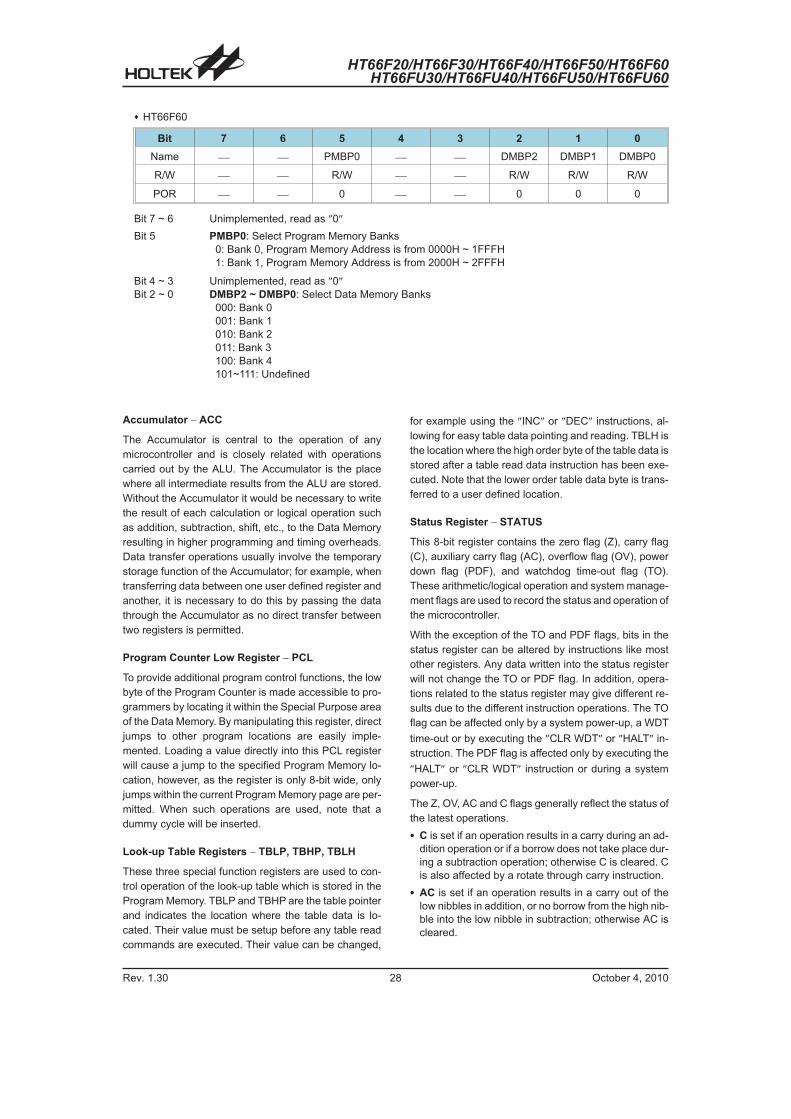
HT66F20/HT66F30/HT66F40/HT66F50/HT66F60HT66FU30/HT66FU40/HT66FU50/HT66FU60
Rev. 1.30 28 October 4, 2010
HT66F60
Bit 7 6 5 4 3 2 1 0
Name � � PMBP0 � � DMBP2 DMBP1 DMBP0
R/W � � R/W � � R/W R/W R/W
POR � � 0 � � 0 0 0
Bit 7 ~ 6 Unimplemented, read as �0�
Bit 5 PMBP0: Select Program Memory Banks
0: Bank 0, Program Memory Address is from 0000H ~ 1FFFH
1: Bank 1, Program Memory Address is from 2000H ~ 2FFFH
Bit 4 ~ 3 Unimplemented, read as �0�Bit 2 ~ 0 DMBP2 ~ DMBP0: Select Data Memory Banks
000: Bank 0
001: Bank 1
010: Bank 2
011: Bank 3
100: Bank 4
101~111: Undefined
Accumulator � ACC
The Accumulator is central to the operation of any
microcontroller and is closely related with operations
carried out by the ALU. The Accumulator is the place
where all intermediate results from the ALU are stored.
Without the Accumulator it would be necessary to write
the result of each calculation or logical operation such
as addition, subtraction, shift, etc., to the Data Memory
resulting in higher programming and timing overheads.
Data transfer operations usually involve the temporary
storage function of the Accumulator; for example, when
transferring data between one user defined register and
another, it is necessary to do this by passing the data
through the Accumulator as no direct transfer between
two registers is permitted.
Program Counter Low Register � PCL
To provide additional program control functions, the low
byte of the Program Counter is made accessible to pro-
grammers by locating it within the Special Purpose area
of the Data Memory. By manipulating this register, direct
jumps to other program locations are easily imple-
mented. Loading a value directly into this PCL register
will cause a jump to the specified Program Memory lo-
cation, however, as the register is only 8-bit wide, only
jumps within the current Program Memory page are per-
mitted. When such operations are used, note that a
dummy cycle will be inserted.
Look-up Table Registers � TBLP, TBHP, TBLH
These three special function registers are used to con-
trol operation of the look-up table which is stored in the
Program Memory. TBLP and TBHP are the table pointer
and indicates the location where the table data is lo-
cated. Their value must be setup before any table read
commands are executed. Their value can be changed,
for example using the �INC� or �DEC� instructions, al-
lowing for easy table data pointing and reading. TBLH is
the location where the high order byte of the table data is
stored after a table read data instruction has been exe-
cuted. Note that the lower order table data byte is trans-
ferred to a user defined location.
Status Register � STATUS
This 8-bit register contains the zero flag (Z), carry flag
(C), auxiliary carry flag (AC), overflow flag (OV), power
down flag (PDF), and watchdog time-out flag (TO).
These arithmetic/logical operation and system manage-
ment flags are used to record the status and operation of
the microcontroller.
With the exception of the TO and PDF flags, bits in the
status register can be altered by instructions like most
other registers. Any data written into the status register
will not change the TO or PDF flag. In addition, opera-
tions related to the status register may give different re-
sults due to the different instruction operations. The TO
flag can be affected only by a system power-up, a WDT
time-out or by executing the �CLR WDT� or �HALT� in-
struction. The PDF flag is affected only by executing the
�HALT� or �CLR WDT� instruction or during a system
power-up.
The Z, OV, AC and C flags generally reflect the status of
the latest operations.
� C is set if an operation results in a carry during an ad-
dition operation or if a borrow does not take place dur-
ing a subtraction operation; otherwise C is cleared. C
is also affected by a rotate through carry instruction.
� AC is set if an operation results in a carry out of the
low nibbles in addition, or no borrow from the high nib-
ble into the low nibble in subtraction; otherwise AC is
cleared.

HT66F20/HT66F30/HT66F40/HT66F50/HT66F60HT66FU30/HT66FU40/HT66FU50/HT66FU60
Rev. 1.30 29 October 4, 2010
� Z is set if the result of an arithmetic or logical operation
is zero; otherwise Z is cleared.
� OV is set if an operation results in a carry into the high-
est-order bit but not a carry out of the highest-order bit,
or vice versa; otherwise OV is cleared.
� PDF is cleared by a system power-up or executing the
�CLR WDT� instruction. PDF is set by executing the
�HALT� instruction.
� TO is cleared by a system power-up or executing the
�CLR WDT� or �HALT� instruction. TO is set by a
WDT time-out.
In addition, on entering an interrupt sequence or execut-
ing a subroutine call, the status register will not be
pushed onto the stack automatically. If the contents of
the status registers are important and if the subroutine
can corrupt the status register, precautions must be
taken to correctly save it.
� STATUS Register
Bit 7 6 5 4 3 2 1 0
Name � � TO PDF OV Z AC C
R/W � � R R R/W R/W R/W R/W
POR � � 0 0 x x x x
�x� unknown
Bit 7, 6 Unimplemented, read as �0�
Bit 5 TO: Watchdog Time-Out flag
0: After power up or executing the �CLR WDT� or �HALT� instruction
1: A watchdog time-out occurred.
Bit 4 PDF: Power down flag
0: After power up or executing the �CLR WDT� instruction
1: By executing the �HALT� instruction
Bit 3 OV: Overflow flag
0: no overflow
1: an operation results in a carry into the highest-order bit but not a carry out of the
highest-order bit or vice versa.
Bit 2 Z: Zero flag
0: The result of an arithmetic or logical operation is not zero
1: The result of an arithmetic or logical operation is zero
Bit 1 AC: Auxiliary flag
0: no auxiliary carry
1: an operation results in a carry out of the low nibbles in addition, or no borrow from the
high nibble into the low nibble in subtraction
Bit 0 C: Carry flag
0: no carry-out
1: an operation results in a carry during an addition operation or if a borrow does not take place
during a subtraction operation
C is also affected by a rotate through carry instruction.

HT66F20/HT66F30/HT66F40/HT66F50/HT66F60HT66FU30/HT66FU40/HT66FU50/HT66FU60
Rev. 1.30 30 October 4, 2010
EEPROM Data Memory
The device contains an area of internal EEPROM Data
Memory. EEPROM, which stands for Electrically Eras-
able Programmable Read Only Memory, is by its nature
a non-volatile form of re-programmable memory, with
data retention even when its power supply is removed.
By incorporating this kind of data memory, a whole new
host of application possibilities are made available to the
designer. The availability of EEPROM storage allows in-
formation such as product identification numbers, cali-
bration values, specific user data, system setup data or
other product information to be stored directly within the
product microcontroller. The process of reading and
writing data to the EEPROM memory has been reduced
to a very trivial affair.
EEPROM Data Memory Structure
The EEPROM Data Memory capacity varies from 32x8
to 256�8 bits, according to the device selected. Unlike
the Program Memory and RAM Data Memory, the
EEPROM Data Memory is not directly mapped into
memory space and is therefore not directly addressable
in the same way as the other types of memory. Read
and Write operations to the EEPROM are carried out in
single byte operations using an address and data regis-
ter in Bank 0 and a single control register in Bank 1.
Device Capacity Address
HT66F20 32�8 00H ~ 1FH
HT66F30 64�8 00H ~ 3FH
HT66F40 128�8 00H ~ 7FH
HT66F50/HT66F60 256�8 00H ~ FFH
EEPROM Registers
Three registers control the overall operation of the inter-
nal EEPROM Data Memory. These are the address reg-
ister, EEA, the data register, EED and a single control
register, EEC. As both the EEA and EED registers are lo-
cated in Bank 0, they can be directly accessed in the
same was as any other Special Function Register. The
EEC register however, being located in Bank1, cannot be
directly addressed directly and can only be read from or
written to indirectly using the MP1 Memory Pointer and
Indirect Addressing Register, IAR1. Because the EEC
control register is located at address 40H in Bank 1, the
MP1 Memory Pointer must first be set to the value 40H
and the Bank Pointer register, BP, set to the value, 01H,
before any operations on the EEC register are executed.
� EEPROM Register List
HT66F20
NameBit
7 6 5 4 3 2 1 0
EEA � � � D4 D3 D2 D1 D0
EED D7 D6 D5 D4 D3 D2 D1 D0
EEC � � � � WREN WR RDEN RD
HT66F30
NameBit
7 6 5 4 3 2 1 0
EEA � � D5 D4 D3 D2 D1 D0
EED D7 D6 D5 D4 D3 D2 D1 D0
EEC � � � � WREN WR RDEN RD
HT66F40
NameBit
7 6 5 4 3 2 1 0
EEA � D6 D5 D4 D3 D2 D1 D0
EED D7 D6 D5 D4 D3 D2 D1 D0
EEC � � � � WREN WR RDEN RD
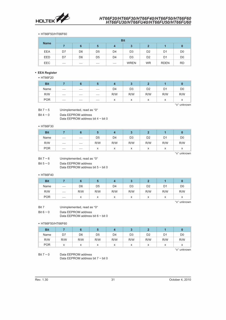
HT66F20/HT66F30/HT66F40/HT66F50/HT66F60HT66FU30/HT66FU40/HT66FU50/HT66FU60
Rev. 1.30 31 October 4, 2010
HT66F50/HT66F60
NameBit
7 6 5 4 3 2 1 0
EEA D7 D6 D5 D4 D3 D2 D1 D0
EED D7 D6 D5 D4 D3 D2 D1 D0
EEC � � � � WREN WR RDEN RD
� EEA Register
HT66F20
Bit 7 6 5 4 3 2 1 0
Name � � � D4 D3 D2 D1 D0
R/W � � � R/W R/W R/W R/W R/W
POR � � � x x x x x
�x� unknown
Bit 7 ~ 5 Unimplemented, read as �0�
Bit 4 ~ 0 Data EEPROM address
Data EEPROM address bit 4 ~ bit 0
HT66F30
Bit 7 6 5 4 3 2 1 0
Name � � D5 D4 D3 D2 D1 D0
R/W � � R/W R/W R/W R/W R/W R/W
POR � � x x x x x x
�x� unknown
Bit 7 ~ 6 Unimplemented, read as �0�
Bit 5 ~ 0 Data EEPROM address
Data EEPROM address bit 5 ~ bit 0
HT66F40
Bit 7 6 5 4 3 2 1 0
Name � D6 D5 D4 D3 D2 D1 D0
R/W � R/W R/W R/W R/W R/W R/W R/W
POR � x x x x x x x
�x� unknown
Bit 7 Unimplemented, read as �0�
Bit 6 ~ 0 Data EEPROM address
Data EEPROM address bit 6 ~ bit 0
HT66F50/HT66F60
Bit 7 6 5 4 3 2 1 0
Name D7 D6 D5 D4 D3 D2 D1 D0
R/W R/W R/W R/W R/W R/W R/W R/W R/W
POR x x x x x x x x
�x� unknown
Bit 7 ~ 0 Data EEPROM address
Data EEPROM address bit 7 ~ bit 0

HT66F20/HT66F30/HT66F40/HT66F50/HT66F60HT66FU30/HT66FU40/HT66FU50/HT66FU60
Rev. 1.30 32 October 4, 2010
� EEC Register
Bit 7 6 5 4 3 2 1 0
Name � � � � WREN WR RDEN RD
R/W � � � � R/W R/W R/W R/W
POR � � � � 0 0 0 0
Bit 7 ~ 4 Unimplemented, read as �0�
Bit 3 WREN: Data EEPROM Write Enable
0: Disable
1: Enable
This is the Data EEPROM Write Enable Bit which must be set high before Data EEPROM write
operations are carried out. Clearing this bit to zero will inhibit Data EEPROM write operations.
Bit 2 WR: EEPROM Write Control
0: Write cycle has finished
1: Activate a write cycle
This is the Data EEPROM Write Control Bit and when set high by the application program will
activate a write cycle. This bit will be automatically reset to zero by the hardware after the write
cycle has finished. Setting this bit high will have no effect if the WREN has not first been set high.
Bit 1 RDEN: Data EEPROM Read Enable
0: Disable
1: Enable
This is the Data EEPROM Read Enable Bit which must be set high before Data EEPROM read
operations are carried out. Clearing this bit to zero will inhibit Data EEPROM read operations.
Bit 0 RD: EEPROM Read Control
0: Read cycle has finished
1: Activate a read cycle
This is the Data EEPROM Read Control Bit and when set high by the application program will
activate a read cycle. This bit will be automatically reset to zero by the hardware after the read
cycle has finished. Setting this bit high will have no effect if the RDEN has not first been set high.
Note: The WREN, WR, RDEN and RD can not be set to �1� at the same time in one instruction. The WR and RD can
not be set to �1� at the same time.
Reading Data from the EEPROM
To read data from the EEPROM, the read enable bit,
RDEN, in the EEC register must first be set high to en-
able the read function. The EEPROM address of the
data to be read must then be placed in the EEA register.
If the RD bit in the EEC register is now set high, a read
cycle will be initiated. Setting the RD bit high will not initi-
ate a read operation if the RDEN bit has not been set.
When the read cycle terminates, the RD bit will be auto-
matically cleared to zero, after which the data can be
read from the EED register. The data will remain in the
EED register until another read or write operation is exe-
cuted. The application program can poll the RD bit to de-
termine when the data is valid for reading.
Writing Data to the EEPROM
To write data to the EEPROM, the write enable bit,
WREN, in the EEC register must first be set high to en-
able the write function. The EEPROM address of the
data to be written must then be placed in the EEA regis-
ter and the data placed in the EED register. If the WR bit
in the EEC register is now set high, an internal write cy-
cle will then be initiated. Setting the WR bit high will not
initiate a write cycle if the WREN bit has not been set. As
the EEPROM write cycle is controlled using an internal
t imer whose operat ion is asynchronous to
microcontroller system clock, a certain time will elapse
before the data will have been written into the EEPROM.
Detecting when the write cycle has finished can be im-
plemented either by polling the WR bit in the EEC regis-
ter or by using the EEPROM interrupt. When the write
cycle terminates, the WR bit will be automatically
cleared to zero by the microcontroller, informing the
user that the data has been written to the EEPROM. The
application program can therefore poll the WR bit to de-
termine when the write cycle has ended.

HT66F20/HT66F30/HT66F40/HT66F50/HT66F60HT66FU30/HT66FU40/HT66FU50/HT66FU60
Rev. 1.30 33 October 4, 2010
Write Protection
Protection against inadvertent write operation is pro-
vided in several ways. After the device is powered-on
the Write Enable bit in the control register will be cleared
preventing any write operations. Also at power-on the
Bank Pointer, BP, will be reset to zero, which means that
Data Memory Bank 0 will be selected. As the EEPROM
control register is located in Bank 1, this adds a further
measure of protection against spurious write opera-
tions. During normal program operation, ensuring that
the Write Enable bit in the control register is cleared will
safeguard against incorrect write operations.
EEPROM Interrupt
The EEPROM write or read interrupt is generated when
an EEPROM write or read cycle has ended. The
EEPROM interrupt must first be enabled by setting the
DEE bit in the relevant interrupt register. However as the
EEPROM is contained within a Multi-function Interrupt,
the associated multi-function interrupt enable bit must
also be set. When an EEPROM write cycle ends, the
DEF request flag and its associated multi-function inter-
rupt request flag will both be set. If the global, EEPROM
and Multi-function interrupts are enabled and the stack
is not full, a jump to the associated Multi-function Inter-
rupt vector will take place. When the interrupt is serviced
only the Multi-function interrupt flag will be automatically
reset, the EEPROM interrupt flag must be manually re-
set by the application program. More details can be ob-
tained in the Interrupt section.
Programming Considerations
Care must be taken that data is not inadvertently written
to the EEPROM. Protection can be enhanced by ensur-
ing that the Write Enable bit is normally cleared to zero
when not writing. Also the Bank Pointer could be nor-
mally cleared to zero as this would inhibit access to
Bank 1 where the EEPROM control register exist. Al-
though certainly not necessary, consideration might be
given in the application program to the checking of the
validity of new write data by a simple read back process.
� Programming Examples
Reading data from the EEPROM - polling method
MOV A, EEPROM_ADRES ; user defined addressMOV EEA, AMOV A, 040H ; setup memory pointer MP1MOV MP1, A ; MP1 points to EEC registerMOV A, 01H ; setup Bank PointerMOV BP, ASET IAR1.1 ; set RDEN bit, enable read operationsSET IAR1.0 ; start Read Cycle - set RD bitBACK:SZ IAR1.0 ; check for read cycle endJMP BACKCLR IAR1 ; disable EEPROM read/writeCLR BPMOV A, EEDATA ; move read data to registerMOV READ_DATA, A
Writing Data to the EEPROM � polling methodMOV A, EEPROM_ADRES ; user defined addressMOV EEA, AMOV A, EEPROM_DATA ; user defined dataMOV EED, AMOV A, 040H ; setup memory pointer MP1MOV MP1, A ; MP1 points to EEC registerMOV A, 01H ; setup Bank PointerMOV BP, ASET IAR1.3 ; set WREN bit, enable write operationsSET IAR1.2 ; start Write Cycle - set WR bitBACK:SZ IAR1.2 ; check for write cycle endJMP BACKCLR IAR1 ; disable EEPROM read/writeCLR BP

HT66F20/HT66F30/HT66F40/HT66F50/HT66F60HT66FU30/HT66FU40/HT66FU50/HT66FU60
Rev. 1.30 34 October 4, 2010
Oscillator
Various oscillator options offer the user a wide range of
functions according to their various application require-
ments. The flexible features of the oscillator functions
ensure that the best optimisation can be achieved in
terms of speed and power saving. Oscillator selections
and operation are selected through a combination of
configuration options and registers.
Oscillator Overview
In addition to being the source of the main system clock
the oscillators also provide clock sources for the Watch-
dog Timer and Time Base Interrupts. External oscilla-
tors requiring some external components as well as fully
integrated internal oscillators, requiring no external
components, are provided to form a wide range of both
fast and slow system oscillators. All oscillator options
are selected through the configuration options. The
higher frequency oscillators provide higher performance
but carry with it the disadvantage of higher power re-
quirements, while the opposite is of course true for the
lower frequency oscillators. With the capability of dy-
namically switching between fast and slow system
clock, the device has the flexibility to optimize the perfor-
mance/power ratio, a feature especially important in
power sensitive portable applications.
Type Name Freq. Pins
External Crystal HXT400kHz~
20MHz
OSC1/
OSC2
External RC ERC 8MHz OSC1
Internal High
Speed RCHIRC 4, 8 or 12MHz �
External Low
Speed CrystalLXT 32.768kHz
XT1/
XT2
Internal Low
Speed RCLIRC 32kHz �
Oscillator Types
System Clock Configurations
There are five methods of generating the system clock,
three high speed oscillators and two low speed oscilla-
tors. The high speed oscillators are the external crystal/
ceramic oscillator, external RC network oscillator and
the internal 4MHz, 8MHz or 12MHz RC oscillator. The
two low speed oscillators are the internal 32kHz RC os-
cillator and the external 32.768kHz crystal oscillator. Se-
lecting whether the low or high speed oscillator is used
as the system oscillator is implemented using the
HLCLK bit and CKS2 ~ CKS0 bits in the SMOD register
and as the system clock can be dynamically selected.
HXT
ERC
HIRC
LIRC
LXT
6-stage Prescaler
High Speed Oscillation
Low Speed Oscillation
Low Speed Oscillation
Configuration Option
High Speed Oscillation
Configuration Option
fH
fH/2
fH/4
fH/8
fH/16
fH/32
fH/64
fL
HLCLK,
CKS2~CKS0 bits
Fast Wake-up from SLEEP Mode or
IDLE Mode Control (for HXT only)
fSYS
fSUB
System Clock Configurations

HT66F20/HT66F30/HT66F40/HT66F50/HT66F60HT66FU30/HT66FU40/HT66FU50/HT66FU60
Rev. 1.30 35 October 4, 2010
The actual source clock used for each of the high speed
and low speed oscillators is chosen via configuration
options. The frequency of the slow speed or high speed
system clock is also determined using the HLCLK bit
and CKS2 ~ CKS0 bits in the SMOD register. Note that
two oscillator selections must be made namely one high
speed and one low speed system oscillators. It is not
possible to choose a no-oscillator selection for either the
high or low speed oscillator.
External Crystal/ Ceramic Oscillator � HXT
The External Crystal/ Ceramic System Oscillator is one
of the high frequency oscillator choices, which is se-
lected via configuration option. For most crystal oscilla-
tor configurations, the simple connection of a crystal
across OSC1 and OSC2 will create the necessary
phase shift and feedback for oscillation, without requir-
ing external capacitors. However, for some crystal types
and frequencies, to ensure oscillation, it may be neces-
sary to add two small value capacitors, C1 and C2.
Using a ceramic resonator will usually require two small
value capacitors, C1 and C2, to be connected as shown
for oscillation to occur. The values of C1 and C2 should
be selected in consultation with the crystal or resonator
manufacturer�s specification.
Crystal Oscillator C1 and C2 Values
Crystal Frequency C1 C2
12MHz 0pF 0pF
8MHz 0pF 0pF
4MHz 0pF 0pF
1MHz 100pF 100pF
Note: C1 and C2 values are for guidance only.
Crystal Recommended Capacitor Values
External RC Oscillator � ERC
Using the ERC oscillator only requires that a resistor,
with a value between 56k� and 2.4M�, is connected
between OSC1 and VDD, and a capacitor is connected
between OSC1 and ground, providing a low cost oscilla-
tor configuration. It is only the external resistor that de-
termines the oscillation frequency; the external
capacitor has no influence over the frequency and is
connected for stability purposes only. Device trimming
during the manufacturing process and the inclusion of
internal frequency compensation circuits are used to en-
sure that the influence of the power supply voltage, tem-
perature and process variations on the oscillation
frequency are minimised. As a resistance/frequency ref-
erence point, it can be noted that with an external 120k�resistor connected and with a 5V voltage power supply
and temperature of 25�C degrees, the oscillator will
have a frequency of 8MHz within a tolerance of 2%.
Here only the OSC1 pin is used, which is shared with I/O
pin PB1, leaving pin PB2 free for use as a normal I/O
pin.
Internal RC Oscillator � HIRC
The internal RC oscillator is a fully integrated system os-
cillator requiring no external components. The internal
RC oscillator has three fixed frequencies of either
4MHz, 8MHz or 12MHz. Device trimming during the
manufacturing process and the inclusion of internal fre-
quency compensation circuits are used to ensure that
the influence of the power supply voltage, temperature
and process variations on the oscillation frequency are
minimised. As a result, at a power supply of either 3V or
5V and at a temperature of 25�C degrees, the fixed os-
cillation frequency of 4MHz, 8MHz or 12MHz will have a
tolerance within 2%. Note that if this internal system
clock option is selected, as it requires no external pins
for its operation, I/O pins PB1 and PB2 are free for use
as normal I/O pins.
External 32.768kHz Crystal Oscillator � LXT
The External 32.768kHz Crystal System Oscillator is
one of the low frequency oscillator choices, which is se-
lected via configuration option. This clock source has a
fixed frequency of 32.768kHz and requires a 32.768kHz
crystal to be connected between pins XT1 and XT2. The
external resistor and capacitor components connected
to the 32.768kHz crystal are necessary to provide oscil-
lation. For applications where precise frequencies are
essential, these components may be required to provide
frequency compensation due to different crystal manu-
facturing tolerances. During power-up there is a time
delay associated with the LXT oscillator waiting for it to
start-up.
� � � �
� � �
� � �
� � �
External RC Oscillator � ERC
� � � �
� � � �
�
� � � � � � � � � � �� � � � � � � �
� � � � � � � �
� � � � � � �
� � � � � � �
� �
� �
� � � � � � � � � � � � � � � � � � ! � � � � � � � " � � � � # � � � � � � � # � � � � � � � � � � " � � � � # �� � � $ � � % � � & % � � � � � � % � ' � � � � � � ( � � � � � � � � � % � ) � � � � � � � � � � � �� � � � � � � � � � � � � � � � � � � � � � � # � � �
Crystal/Resonator Oscillator � HXT

HT66F20/HT66F30/HT66F40/HT66F50/HT66F60HT66FU30/HT66FU40/HT66FU50/HT66FU60
Rev. 1.30 36 October 4, 2010
When the microcontroller enters the SLEEP or IDLE
Mode, the system clock is switched off to stop
microcontroller activity and to conserve power. How-
ever, in many microcontroller applications it may be nec-
essary to keep the internal timers operational even
when the microcontroller is in the SLEEP or IDLE Mode.
To do this, another clock, independent of the system
clock, must be provided.
However, for some crystals, to ensure oscillation and
accurate frequency generation, it is necessary to add
two small value external capacitors, C1 and C2. The ex-
act values of C1 and C2 should be selected in consulta-
tion with the crystal or resonator manufacturer�sspecification. The external parallel feedback resistor,
Rp, is required.
Some configuration options determine if the XT1/XT2
pins are used for the LXT oscillator or as I/O pins.
� If the LXT oscillator is not used for any clock source,
the XT1/XT2 pins can be used as normal I/O pins.
� If the LXT oscillator is used for any clock source, the
32.768kHz crystal should be connected to the
XT1/XT2 pins.
LXT Oscillator C1 and C2 Values
Crystal Frequency C1 C2
32.768kHz 10pF 10pF
Note: 1. C1 and C2 values are for guidance only.
2. RP=5M~10M� is recommended.
32.768kHz Crystal Recommended Capacitor Values
LXT Oscillator Low Power Function
The LXT oscillator can function in one of two modes, the
Quick Start Mode and the Low Power Mode. The mode
selection is executed using the LXTLP bit in the TBC
register.
LXTLP Bit LXT Mode
0 Quick Start
1 Low-power
After power on the LXTLP bit will be automatically
cleared to zero ensuring that the LXT oscillator is in the
Quick Start operating mode. In the Quick Start Mode the
LXT oscillator will power up and stabilise quickly. How-
ever, after the LXT oscillator has fully powered up it can
be placed into the Low-power mode by setting the
LXTLP bit high. The oscillator will continue to run but
with reduced current consumption, as the higher current
consumption is only required during the LXT oscillator
start-up. In power sensitive applications, such as battery
applications, where power consumption must be kept to
a minimum, it is therefore recommended that the appli-
cation program sets the LXTLP bit high about 2 seconds
after power-on.
It should be noted that, no matter what condition the
LXTLP bit is set to, the LXT oscillator will always func-
tion normally, the only difference is that it will take more
time to start up if in the Low-power mode.
Internal 32kHz Oscillator � LIRC
The Internal 32kHz System Oscillator is one of the low
frequency oscillator choices, which is selected via con-
figuration option. It is a fully integrated RC oscillator with
a typical frequency of 32kHz at 5V, requiring no external
components for its implementation. Device trimming
during the manufacturing process and the inclusion of
internal frequency compensation circuits are used to en-
sure that the influence of the power supply voltage, tem-
perature and process variations on the oscillation
frequency are minimised. As a result, at a power supply
of 5V and at a temperature of 25�C degrees, the fixed
oscillation frequency of 32kHz will have a tolerance
within 10%.
Supplementary Oscillators
The low speed oscillators, in addition to providing a sys-
tem clock source are also used to provide a clock
source to two other device functions. These are the
Watchdog Timer and the Time Base Interrupts.
� � � � � � � � � � �� � � � � � � �
� � � � � � � �
� � � � � � �
� � � � � � �
� �
� �
� � � � � � � � * � � � � � � # � � � � � � � � � � " � � � � # �� � � $ � � % � � & % � � � � � � % � ' � � � � � � % � ) � � �� � � � � � � � � � � � � � � � � � � � � � � � � � � � � � � � # � � �
+ � � � � � � � � �� � � � � � � � � �
, � � � - ./ 0 1
2 � �
2 � �
External LXT Oscillator

HT66F20/HT66F30/HT66F40/HT66F50/HT66F60HT66FU30/HT66FU40/HT66FU50/HT66FU60
Rev. 1.30 37 October 4, 2010
Operating Modes and System Clocks
Present day appl icat ions require that their
microcontrollers have high performance but often still
demand that they consume as little power as possible,
conflicting requirements that are especially true in bat-
tery powered portable applications. The fast clocks re-
quired for high performance will by their nature increase
current consumption and of course vice-versa, lower
speed clocks reduce current consumption. As Holtek
has provided these devices with both high and low
speed clock sources and the means to switch between
them dynamically, the user can optimise the operation of
their microcontroller to achieve the best perfor-
mance/power ratio.
System Clocks
The device has many different clock sources for both
the CPU and peripheral function operation. By providing
the user with a wide range of clock options using config-
uration options and register programming, a clock sys-
tem can be configured to obtain maximum application
performance.
The main system clock, can come from either a high fre-
quency, fH, or low frequency, fL, source, and is selected
using the HLCLK bit and CKS2~CKS0 bits in the SMOD
register. The high speed system clock can be sourced
from either an HXT, ERC or HIRC oscillator, selected via
a configuration option. The low speed system clock
source can be sourced from internal clock fL. If fL is se-
lected then it can be sourced by either the LXT or LIRC
oscillators, selected via a configuration option. The
other choice, which is a divided version of the high
speed system oscillator has a range of fH/2~fH/64.
There are two additional internal clocks for the periph-
eral circuits, the substitute clock, fSUB, and the Time
Base clock, fTBC. Each of these internal clocks are
sourced by either the LXT or LIRC oscillators, selected
via configuration options. The fSUB clock is used to pro-
vide a substitute clock for the microcontroller just after a
wake-up has occurred to enable faster wake-up times.
fTBC
fSYS/4
TBCK
fSUB
fSYS/4
fTB
fS
Configuration Option
Time Base
WDT
HXT
ERC
HIRC
LIRC
LXT
6-stage Prescaler
High Speed Oscillation
Low Speed Oscillation
Low Speed Oscillat ion
Configuration Option
High Speed OscillationConfiguration Option
fH
fH/2
fH/4
fH/8
fH/16
fH/32
fH/64
fL
HLCLK,
CKS2~CKS0 bits
Fast Wake-up from SLEEP Mode or
IDLE Mode Control (for HXT only)
fSYS
fSUB
System Clock Configurations
Note: When the system clock source fSYS is switched to fL from fH, the high speed oscillation will stop to conserve the
power. Thus there is no fH~fH/64 for peripheral circuit to use.
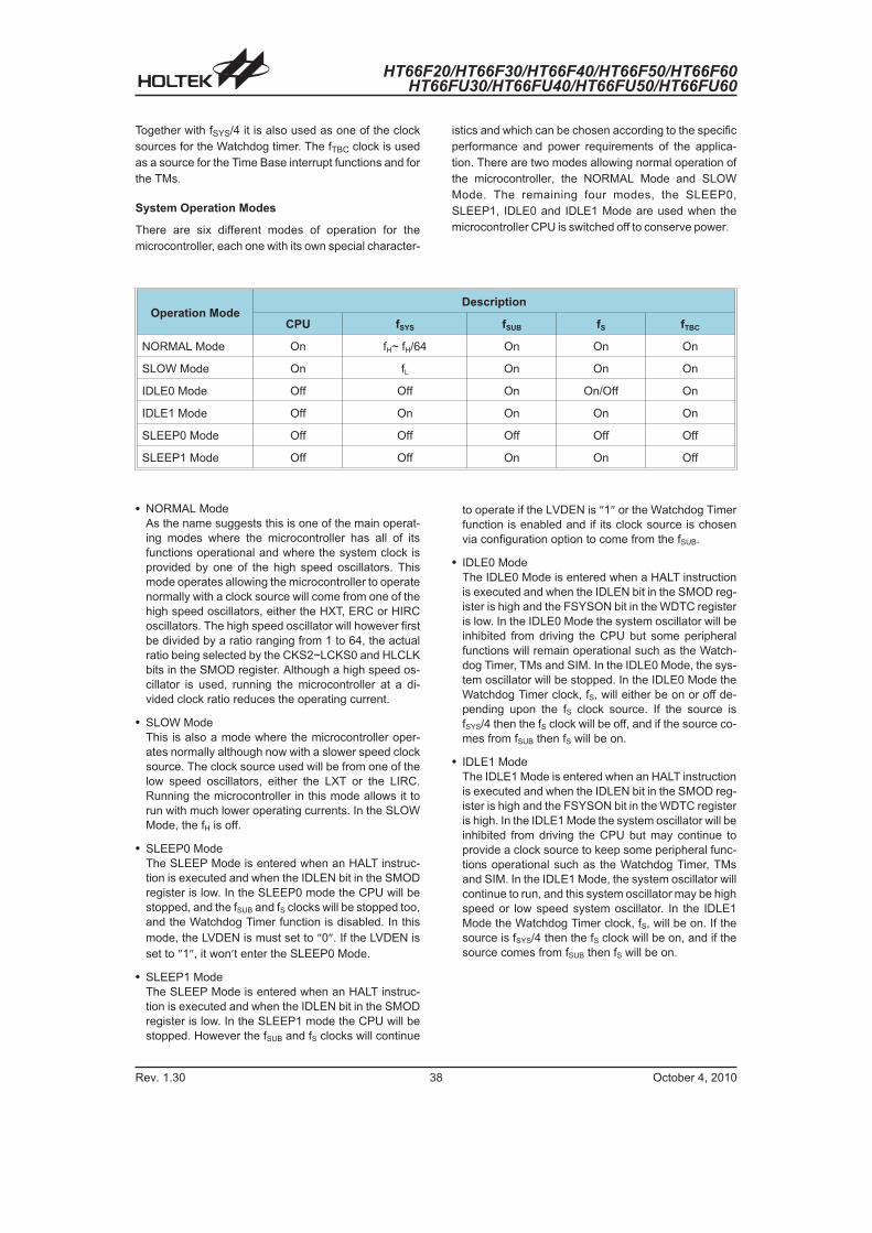
HT66F20/HT66F30/HT66F40/HT66F50/HT66F60HT66FU30/HT66FU40/HT66FU50/HT66FU60
Rev. 1.30 38 October 4, 2010
Together with fSYS/4 it is also used as one of the clock
sources for the Watchdog timer. The fTBC clock is used
as a source for the Time Base interrupt functions and for
the TMs.
System Operation Modes
There are six different modes of operation for the
microcontroller, each one with its own special character-
istics and which can be chosen according to the specific
performance and power requirements of the applica-
tion. There are two modes allowing normal operation of
the microcontroller, the NORMAL Mode and SLOW
Mode. The remaining four modes, the SLEEP0,
SLEEP1, IDLE0 and IDLE1 Mode are used when the
microcontroller CPU is switched off to conserve power.
Operation ModeDescription
CPU fSYS fSUB fS fTBC
NORMAL Mode On fH~ fH/64 On On On
SLOW Mode On fL On On On
IDLE0 Mode Off Off On On/Off On
IDLE1 Mode Off On On On On
SLEEP0 Mode Off Off Off Off Off
SLEEP1 Mode Off Off On On Off
� NORMAL Mode
As the name suggests this is one of the main operat-
ing modes where the microcontroller has all of its
functions operational and where the system clock is
provided by one of the high speed oscillators. This
mode operates allowing the microcontroller to operate
normally with a clock source will come from one of the
high speed oscillators, either the HXT, ERC or HIRC
oscillators. The high speed oscillator will however first
be divided by a ratio ranging from 1 to 64, the actual
ratio being selected by the CKS2~LCKS0 and HLCLK
bits in the SMOD register. Although a high speed os-
cillator is used, running the microcontroller at a di-
vided clock ratio reduces the operating current.
� SLOW Mode
This is also a mode where the microcontroller oper-
ates normally although now with a slower speed clock
source. The clock source used will be from one of the
low speed oscillators, either the LXT or the LIRC.
Running the microcontroller in this mode allows it to
run with much lower operating currents. In the SLOW
Mode, the fH is off.
� SLEEP0 Mode
The SLEEP Mode is entered when an HALT instruc-
tion is executed and when the IDLEN bit in the SMOD
register is low. In the SLEEP0 mode the CPU will be
stopped, and the fSUB and fS clocks will be stopped too,
and the Watchdog Timer function is disabled. In this
mode, the LVDEN is must set to �0�. If the LVDEN is
set to �1�, it won�t enter the SLEEP0 Mode.
� SLEEP1 Mode
The SLEEP Mode is entered when an HALT instruc-
tion is executed and when the IDLEN bit in the SMOD
register is low. In the SLEEP1 mode the CPU will be
stopped. However the fSUB and fS clocks will continue
to operate if the LVDEN is �1� or the Watchdog Timer
function is enabled and if its clock source is chosen
via configuration option to come from the fSUB.
� IDLE0 Mode
The IDLE0 Mode is entered when a HALT instruction
is executed and when the IDLEN bit in the SMOD reg-
ister is high and the FSYSON bit in the WDTC register
is low. In the IDLE0 Mode the system oscillator will be
inhibited from driving the CPU but some peripheral
functions will remain operational such as the Watch-
dog Timer, TMs and SIM. In the IDLE0 Mode, the sys-
tem oscillator will be stopped. In the IDLE0 Mode the
Watchdog Timer clock, fS, will either be on or off de-
pending upon the fS clock source. If the source is
fSYS/4 then the fS clock will be off, and if the source co-
mes from fSUB then fS will be on.
� IDLE1 Mode
The IDLE1 Mode is entered when an HALT instruction
is executed and when the IDLEN bit in the SMOD reg-
ister is high and the FSYSON bit in the WDTC register
is high. In the IDLE1 Mode the system oscillator will be
inhibited from driving the CPU but may continue to
provide a clock source to keep some peripheral func-
tions operational such as the Watchdog Timer, TMs
and SIM. In the IDLE1 Mode, the system oscillator will
continue to run, and this system oscillator may be high
speed or low speed system oscillator. In the IDLE1
Mode the Watchdog Timer clock, fS, will be on. If the
source is fSYS/4 then the fS clock will be on, and if the
source comes from fSUB then fS will be on.

HT66F20/HT66F30/HT66F40/HT66F50/HT66F60HT66FU30/HT66FU40/HT66FU50/HT66FU60
Rev. 1.30 39 October 4, 2010
Control Register
A single register, SMOD, is used for overall control of the internal clocks within the device.
� SMOD Register
Bit 7 6 5 4 3 2 1 0
Name CKS2 CKS1 CKS0 FSTEN LTO HTO IDLEN HLCLK
R/W R/W R/W R/W R/W R R R/W R/W
POR 0 0 0 0 0 0 1 1
Bit 7~5 CKS2~CKS0: The system clock selection when HLCLK is �0�000: fL (fLXT or fLIRC)
001: fL (fLXT or fLIRC)
010: fH/64
011: fH/32
100: fH/16
101: fH/8
110: fH/4
111: fH/2
These three bits are used to select which clock is used as the system clock source. In addition
to the system clock source, which can be either the LXT or LIRC, a divided version of the high
speed system oscillator can also be chosen as the system clock source.
Bit 4 FSTEN: Fast Wake-up Control (only for HXT)
0: Disable
1: Enable
This is the Fast Wake-up Control bit which determines if the fSUB clock source is initially used
after the device wakes up. When the bit is high, the fSUB clock source can be used as a
temporary system clock to provide a faster wake up time as the fSUB clock is available.
Bit 3 LTO: Low speed system oscillator ready flag
0: Not ready
1: Ready
This is the low speed system oscillator ready flag which indicates when the low speed system
oscillator is stable after power on reset or a wake-up has occurred. The flag will be low when in
the SLEEP0 Mode but after a wake-up has occurred, the flag will change to a high level after
1024 clock cycles if the LXT oscillator is used and 1~2 clock cycles if the LIRC oscillator is used.
Bit 2 HTO: High speed system oscillator ready flag
0: Not ready
1: Ready
This is the high speed system oscillator ready flag which indicates when the high speed system
oscillator is stable. This flag is cleared to �0� by hardware when the device is powered on and
then changes to a high level after the high speed system oscillator is stable. Therefore this flag
will always be read as �1� by the application program after device power-on. The flag will be
low when in the SLEEP or IDLE0 Mode but after a wake-up has occurred, the flag will change to
a high level after 1024 clock cycles if the HXT oscillator is used and after 15~16 clock cycles if
the ERC or HIRC oscillator is used.
Bit 1 IDLEN: IDLE Mode control
0: Disable
1: Enable
This is the IDLE Mode Control bit and determines what happens when the HALT instruction is
executed. If this bit is high, when a HALT instruction is executed the device will enter the
IDLE Mode. In the IDLE1 Mode the CPU will stop running but the system clock will continue to
keep the peripheral functions operational, if FSYSON bit is high. If FSYSON bit is low, the CPU
and the system clock will all stop in IDLE0 mode. If the bit is low the device will enter the
SLEEP Mode when a HALT instruction is executed.
Bit 0 HLCLK: system clock selection
0: fH/2 ~ fH/64 or fL1: fH
This bit is used to select if the fH clock or the fH/2 ~ fH/64 or fL clock is used as the system
clock. When the bit is high the fH clock will be selected and if low the fH/2 ~ fH/64 or fL clock will
be selected. When system clock switches from the fH clock to the fL clock and the fH clock will
be automatically switched off to conserve power.

HT66F20/HT66F30/HT66F40/HT66F50/HT66F60HT66FU30/HT66FU40/HT66FU50/HT66FU60
Rev. 1.30 40 October 4, 2010
Fast Wake-up
To minimise power consumption the device can enter
the SLEEP or IDLE0 Mode, where the system clock
source to the device will be stopped. However when the
device is woken up again, it can take a considerable
time for the original system oscillator to restart, stabilise
and allow normal operation to resume. To ensure the
device is up and running as fast as possible a Fast
Wake-up function is provided, which allows fSUB,
namely either the LXT or LIRC oscillator, to act as a tem-
porary clock to first drive the system until the original
system oscillator has stabilised. As the clock source for
the Fast Wake-up function is fSUB, the Fast Wake-up
function is only available in the SLEEP1 and IDLE0
modes. When the device is woken up from the SLEEP0
mode, the Fast Wake-up function has no effect because
the fSUB clock is stopped. The Fast Wake-up enable/dis-
able function is controlled using the FSTEN bit in the
SMOD register.
If the HXT oscillator is selected as the NORMAL Mode
system clock, and if the Fast Wake-up function is en-
abled, then it will take one to two tSUB clock cycles of the
LIRC or LXT oscillator for the system to wake-up. The
system will then initially run under the fSUB clock source
until 1024 HXT clock cycles have elapsed, at which
point the HTO flag will switch high and the system will
switch over to operating from the HXT oscillator.
If the ERC or HIRC oscillators or LIRC oscillator is used
as the system oscillator then it will take 15~16 clock cy-
cles of the ERC or HIRC or 1~2 cycles of the LIRC to
wake up the system from the SLEEP or IDLE0 Mode.
The Fast Wake-up bit, FSTEN will have no effect in
these cases.
System
Oscillator
FSTEN
Bit
Wake-up Time
(SLEEP0 Mode)
Wake-up Time
(SLEEP1 Mode)
Wake-up Time
(IDLE0 Mode)
Wake-up Time
(IDLE1 Mode)
HXT
0 1024 HXT cycles 1024 HXT cycles 1~2 HXT cycles
1 1024 HXT cycles
1~2 fSUB cycles
(System runs with fSUB first for 1024 HXT cycles
and then switches over to run with the HXT clock)
1~2 HXT cycles
ERC X 15~16 ERC cycles 15~16 ERC cycles 1~2 ERC cycles
HIRC X 15~16 HIRC cycles 15~16 HIRC cycles 1~2 HIRC cycles
LIRC X 1~2 LIRC cycles 1~2 LIRC cycles 1~2 LIRC cycles
LXT X 1024 LTX cycles 1024 LXT cycles 1~2 LXT cycles
Wake-Up Times
Note that if the Watchdog Timer is disabled, which means that the LXT and LIRC are all both off, then there will be no
Fast Wake-up function available when the device wakes-up from the SLEEP0 Mode.
� � � � � �
0 $ 3 � � � � � � � � � � � � � � � � � � 4 � � � � � #� � 5 � � � � �
� 6 7 � � � � + � 3 8 � 9 �� � : � � � � �� � 7 : � � � �
; � � � < � 3 � � � � � �
� � � � �
� � 5 � 9 � 0 = � 0 ( - �� 0 � � �
� 6 7 � � � �� � 5 � � � �� � : � � � �� � 7 : � � �
� � � � �
0 $ 3 � � � � � � � � � � � � � � � � � � 4 � � � � � #� 6 7 � � � � + � 3 8 � 9 �
� 5 � � � 9 �� � 5 � � � �� � : � � � �� � 7 : � � � �
� � � � �
0 $ 3 � � � � � � � � � � � � � � � � � � 4 � � � � � #� 6 7 � � � � + � 3 8 � 9 �
� 5 � � � 9 �� � 5 � � � � �� � : � � � �� � 7 : � � �
� � �
� � 5 � 9 � 3� 3 � � �
� 6 7 � � � �� � 5 � � � �� � : � � � �� � 7 : � � �� 0 � � � �
� � � � � �
0 $ 3 � � � � � � � � � � � � � � � � � � 4 � � � � � #� � 5 � � � � �
� 6 7 � � � � + � 3 8 � 9 �� � : � � � � �� � 7 : � � �
; � � � � � � 3 � � � � �

HT66F20/HT66F30/HT66F40/HT66F50/HT66F60HT66FU30/HT66FU40/HT66FU50/HT66FU60
Rev. 1.30 41 October 4, 2010
Operating Mode Switching and Wake-up
The device can switch between operating modes dy-
namically allowing the user to select the best perfor-
mance/power ratio for the present task in hand. In this
way microcontroller operations that do not require high
performance can be executed using slower clocks thus
requiring less operating current and prolonging battery
life in portable applications.
In simple terms, Mode Switching between the NORMAL
Mode and SLOW Mode is executed using the HLCLK bit
and CKS2~CKS0 bits in the SMOD register while Mode
Switching from the NORMAL/SLOW Modes to the
SLEEP/IDLE Modes is executed via the HALT instruc-
tion. When a HALT instruction is executed, whether the
device enters the IDLE Mode or the SLEEP Mode is de-
termined by the condition of the IDLEN bit in the SMOD
register and FSYSON in the WDTC register.
When the HLCLK bit switches to a low level, which im-
plies that clock source is switched from the high speed
clock source, fH, to the clock source, fH/2~fH/64 or fL. If
the clock is from the fL, the high speed clock source will
stop running to conserve power. When this happens it
must be noted that the fH/16 and fH/64 internal clock
sources will also stop running, which may affect the op-
eration of other internal functions such as the TMs and
the SIM. The accompanying flowchart shows what hap-
pens when the device moves between the various oper-
ating modes.
NORMAL Mode to SLOW Mode Switching
When running in the NORMAL Mode, which uses the
high speed system oscillator, and therefore consumes
more power, the system clock can switch to run in the
SLOW Mode by set the HLCLK bit to �0� and set the
CKS2~CKS0 bits to �000� or �001� in the SMOD regis-
ter. This will then use the low speed system oscillator
which will consume less power. Users may decide to do
this for certain operations which do not require high per-
formance and can subsequently reduce power con-
sumption.
The SLOW Mode is sourced from the LXT or the LIRC
oscillators and therefore requires these oscillators to be
stable before full mode switching occurs. This is moni-
tored using the LTO bit in the SMOD register.
� 3 � ; � > � # �
� 3 8 8 6 � � > � # �
� 3 8 8 6 � � > � # �
+ � 8 3 � � > � # �
+ � 3 8 � � > � # �
� � > $ 3 � > � # �
� ? � � � = � � ? � � � 9 � � � 4 : � <0 3 � 3 ? � 9 � �
; � � � � � # � 3 � � � � � � � � � � � � � �+ � 3 8 � � 9 � �0 $ 3 � � � � � � � � � � � � � � � � � � 4 � � � � � #
; � � � � � � 3 � � � � � � � �+ � 3 8 � � 9 � �0 $ 3 � � � � � � � � � � � � � � � � � � 4 � � � � � #
+ � 3 8 � � 9 � � * � � 5 � � � 9 �0 $ 3 � � � � � � � � � � � � � � � � � � 4 � � � � � #
+ � 3 8 � � 9 � � * � � 5 � � � 9 �0 $ 3 � � � � � � � � � � � � � � � � � � 4 � � � � � #

HT66F20/HT66F30/HT66F40/HT66F50/HT66F60HT66FU30/HT66FU40/HT66FU50/HT66FU60
Rev. 1.30 42 October 4, 2010
� � > $ 3 � > � # �
� 3 8 8 6 � � > � # �
� 3 8 8 6 � � > � # �
+ � 3 8 � � > � # �
+ � 3 8 � � > � # �
� 3 � ; � > � # �
� ? � � = � ? � � � � � � : * � � � � : � � � � 0 3 � 3 ? 9 �� � � 0 3 � 3 ? 9 �
; � � � � � # � 3 � � � � � � � � � � � � � �+ � 3 8 � � 9 � �0 $ 3 � � � � � � � � � � � � � � � � � � 4 � � � � � #
; � � � � � � 3 � � � � � � � �+ � 3 8 � � 9 � �0 $ 3 � � � � � � � � � � � � � � � � � � 4 � � � � � #
+ � 3 8 � � 9 � � * � � 5 � � � 9 �0 $ 3 � � � � � � � � � � � � � � � � � � 4 � � � � � #
+ � 3 8 � � 9 � � * � � 5 � � � 9 �0 $ 3 � � � � � � � � � � � � � � � � � � 4 � � � � � #
SLOW Mode to NORMAL Mode Switching
In SLOW Mode the system uses either the LXT or LIRC
low speed system oscillator. To switch back to the
NORMAL Mode, where the high speed system oscillator
is used, the HLCLK bit should be set to �1� or HLCLK bit
is �0�, but CKS2~CKS0 is set to �010�, �011�, �100�,
�101�, �110� or �111�. As a certain amount of time will be
required for the high frequency clock to stabilise, the
status of the HTO bit is checked. The amount of time
required for high speed system oscillator stabilization
depends upon which high speed system oscillator type
is used.
Entering the SLEEP0 Mode
There is only one way for the device to enter the
SLEEP0 Mode and that is to execute the �HALT� instruc-
tion in the application program with the IDLEN bit in
SMOD register equal to �0� and the WDT and LVD both
off. When this instruction is executed under the condi-
tions described above, the following will occur:
� The system clock, WDT clock and Time Base clock
will be stopped and the application program will stop
at the �HALT� instruction.
� The Data Memory contents and registers will maintain
their present condition.
� The WDT will be cleared and stopped no matter if the
WDT clock source originates from the fSUB clock or
from the system clock.
� The I/O ports will maintain their present conditions.
� In the status register, the Power Down flag, PDF, will
be set and the Watchdog time-out flag, TO, will be
cleared.

HT66F20/HT66F30/HT66F40/HT66F50/HT66F60HT66FU30/HT66FU40/HT66FU50/HT66FU60
Rev. 1.30 43 October 4, 2010
Entering the SLEEP1 Mode
There is only one way for the device to enter the
SLEEP1 Mode and that is to execute the �HALT�instruction in the application program with the IDLEN bit
in SMOD register equal to �0� and the WDT or LVD on.
When this instruction is executed under the conditions
described above, the following will occur:
� The system clock and Time Base clock will be
stopped and the application program will stop at the
�HALT� instruction, but the WDT or LVD will remain
with the clock source coming from the fSUB clock.
� The Data Memory contents and registers will maintain
their present condition.
� The WDT will be cleared and resume counting if the
WDT clock source is selected to come from the fSUB
clock as the WDT is enabled.
� The I/O ports will maintain their present conditions.
� In the status register, the Power Down flag, PDF, will
be set and the Watchdog time-out flag, TO, will be
cleared.
Entering the IDLE0 Mode
There is only one way for the device to enter the IDLE0
Mode and that is to execute the �HALT� instruction in the
application program with the IDLEN bit in SMOD register
equal to �1� and the FSYSON bit in WDTC register equal
to �0�. When this instruction is executed under the condi-
tions described above, the following will occur:
� The system clock will be stopped and the application
program will stop at the �HALT� instruction, but the
Time Base clock and fSUB clock will be on.
� The Data Memory contents and registers will maintain
their present condition.
� The WDT will be cleared and resume counting if the
WDT clock source is selected to come from the fSUB
clock and the WDT is enabled. The WDT will stop if its
clock source originates from the system clock.
� The I/O ports will maintain their present conditions.
� In the status register, the Power Down flag, PDF, will
be set and the Watchdog time-out flag, TO, will be
cleared.
Entering the IDLE1 Mode
There is only one way for the device to enter the IDLE1
Mode and that is to execute the �HALT� instruction in the
application program with the IDLEN bit in SMOD register
equal to �1� and the FSYSON bit in WDTC register equal
to �1�. When this instruction is executed under the with
conditions described above, the following will occur:
� The system clock and Time Base clock and fSUB clock
will be on and the application program will stop at the
�HALT� instruction.
� The Data Memory contents and registers will maintain
their present condition.
� The WDT will be cleared and resume counting if the
WDT is enabled regardless of the WDT clock source
which originates from the fSUB clock or from the system
clock.
� The I/O ports will maintain their present conditions.
� In the status register, the Power Down flag, PDF, will
be set and the Watchdog time-out flag, TO, will be
cleared.
Standby Current Considerations
As the main reason for entering the SLEEP or IDLE
Mode is to keep the current consumption of the device
to as low a value as possible, perhaps only in the order
of several micro-amps except in the IDLE1 Mode, there
are other considerations which must also be taken into
account by the circuit designer if the power consumption
is to be minimised. Special attention must be made to
the I/O pins on the device. All high-impedance input pins
must be connected to either a fixed high or low level as
any floating input pins could create internal oscillations
and result in increased current consumption. This also
applies to devices which have different package types,
as there may be unbonbed pins. These must either be
setup as outputs or if setup as inputs must have
pull-high resistors connected.
Care must also be taken with the loads, which are con-
nected to I/O pins, which are setup as outputs. These
should be placed in a condition in which minimum cur-
rent is drawn or connected only to external circuits that
do not draw current, such as other CMOS inputs. Also
note that additional standby current will also be required
if the configuration options have enabled the LXT or
LIRC oscillator.
In the IDLE1 Mode the system oscillator is on, if the sys-
tem oscillator is from the high speed system oscillator,
the additional standby current will also be perhaps in the
order of several hundred micro-amps

HT66F20/HT66F30/HT66F40/HT66F50/HT66F60HT66FU30/HT66FU40/HT66FU50/HT66FU60
Rev. 1.30 44 October 4, 2010
Wake-up
After the system enters the SLEEP or IDLE Mode, it can
be woken up from one of various sources listed as fol-
lows:
� An external reset
� An external falling edge on Port A
� A system interrupt
� A WDT overflow
If the system is woken up by an external reset, the de-
vice will experience a full system reset, however, if the
device is woken up by a WDT overflow, a Watchdog
Timer reset will be initiated. Although both of these
wake-up methods will initiate a reset operation, the ac-
tual source of the wake-up can be determined by exam-
ining the TO and PDF flags. The PDF flag is cleared by a
system power-up or executing the clear Watchdog
Timer instructions and is set when executing the �HALT�instruction. The TO flag is set if a WDT time-out occurs,
and causes a wake-up that only resets the Program
Counter and Stack Pointer, the other flags remain in their
original status.
Each pin on Port A can be setup using the PAWU regis-
ter to permit a negative transition on the pin to wake-up
the system. When a Port A pin wake-up occurs, the pro-
gram will resume execution at the instruction following
the �HALT� instruction. If the system is woken up by an
interrupt, then two possible situations may occur. The first
is where the related interrupt is disabled or the interrupt is
enabled but the stack is full, in which case the program
will resume execution at the instruction following the
�HALT� instruction. In this situation, the interrupt which
woke-up the device will not be immediately serviced, but
will rather be serviced later when the related interrupt is fi-
nally enabled or when a stack level becomes free. The
other situation is where the related interrupt is enabled
and the stack is not full, in which case the regular inter-
rupt response takes place. If an interrupt request flag is
set high before entering the SLEEP or IDLE Mode, the
wake-up function of the related interrupt will be disabled.
Programming Considerations
The HXT and LXT oscillators both use the same SST
counter. For example, if the system is woken up from the
SLEEP0 Mode and both the HXT and LXT oscillators
need to start-up from an off state. The LXT oscillator
uses the SST counter after HXT oscillator has finished
its SST period.
� If the device is woken up from the SLEEP0 Mode to
the NORMAL Mode, the high speed system oscillator
needs an SST period. The device will execute first in-
struction after HTO is �1�. At this time, the LXT oscilla-
tor may not be stability if fSUB is from LXT oscillator. The
same situation occurs in the power-on state. The LXT
oscillator is not ready yet when the first instruction is
executed.
� If the device is woken up from the SLEEP1 Mode to
NORMAL Mode, and the system clock source is from
HXT oscillator and FSTEN is �1�, the system clock can
be switched to the LXT or LIRC oscillator after wake
up.
� There are peripheral functions, such as WDT, TMs
and SIM, for which the fSYS is used. If the system clock
source is switched from fH to fL, the clock source to the
peripheral functions mentioned above will change ac-
cordingly.
� The on/off condition of fSUB and fS depends upon
whether the WDT is enabled or disabled as the WDT
clock source is selected from fSUB.

HT66F20/HT66F30/HT66F40/HT66F50/HT66F60HT66FU30/HT66FU40/HT66FU50/HT66FU60
Rev. 1.30 45 October 4, 2010
Watchdog Timer
The Watchdog Timer is provided to prevent program
malfunctions or sequences from jumping to unknown lo-
cations, due to certain uncontrollable external events
such as electrical noise.
Watchdog Timer Clock Source
The Watchdog Timer clock source is provided by the in-
ternal clock, fS, which is in turn supplied by one of two
sources selected by configuration option: fSUB or fSYS/4.
The fSUB clock can be sourced from either the LXT or
LIRC oscillators, again chosen via a configuration op-
tion. The Watchdog Timer source clock is then subdi-
vided by a ratio of 28 to 215 to give longer timeouts, the
actual value being chosen using the WS2~WS0 bits in
the WDTC register. The LIRC internal oscillator has an
approximate period of 32kHz at a supply voltage of 5V.
However, it should be noted that this specified internal
clock period can vary with VDD, temperature and pro-
cess variations. The LXT oscillator is supplied by an ex-
ternal 32.768kHz crystal. The other Watchdog Timer
clock source option is the fSYS/4 clock. The Watchdog
Timer clock source can originate from its own internal
LIRC oscillator, the LXT oscillator or fSYS/4. It is divided
by a value of 28 to 215, using the WS2~WS0 bits in the
WDTC register to obtain the required Watchdog Timer
time-out period.
Watchdog Timer Control Register
A single register, WDTC, controls the required timeout
period as well as the enable/disable operation. This reg-
ister together with several configuration options control
the overall operation of the Watchdog Timer.
� WDTC Register
Bit 7 6 5 4 3 2 1 0
Name FSYSON WS2 WS1 WS0 WDTEN3 WDTEN2 WDTEN1 WDTEN0
R/W R/W R/W R/W R/W R/W R/W R/W R/W
POR 0 1 1 1 1 0 1 0
Bit 7 FSYSON: fSYS Control in IDLE Mode
0: Disable
1: Enable
Bit 6 ~ 4 WS2, WS1, WS0 : WDT time-out period selection
000: 256/fS001: 512/fS010: 1024/fS011: 2048/fS100: 4096/fS101: 8192/fS110: 16384/fS111: 32768/fS
These three bits determine the division ratio of the Watchdog Timer source clock, which in turn
determines the timeout period.
Bit 3 ~ 0 WDTEN3, WDTEN2, WDTEN1, WDTEN0 : WDT Software Control
1010: Disable
Other: Enable

HT66F20/HT66F30/HT66F40/HT66F50/HT66F60HT66FU30/HT66FU40/HT66FU50/HT66FU60
Rev. 1.30 46 October 4, 2010
. @ � � � & � � � � ) � # � �� �
; � � � � � � @ � � �A � . ( � � � = � � � B ( � � C
� � ( � .
; � � � 6 � � � � � � � �
. @ � � @ � � > 7 2
� � � � � � ; � � � � ! �
� � � � � & � � � � � � � � � � � � �
� 3 � ; � � � � � � &
� 3 � ; � � � � � � &
� � � � � � � + � � � � � � � � � � �� 3 �
� � 7 :
; � � = ; � �A � � ( � . � = � � � ( � � B C
>72
� � 5 � ( �
>72
3 2 �
3 + �
� � � � � & � � � � � � �� � � � �
� � � � � & � � � � � � �� � � � �
Watchdog Timer
Watchdog Timer Operation
The Watchdog Timer operates by providing a device re-
set when its timer overflows. This means that in the ap-
plication program and during normal operation the user
has to strategically clear the Watchdog Timer before it
overflows to prevent the Watchdog Timer from execut-
ing a reset. This is done using the clear watchdog in-
structions. If the program malfunctions for whatever
reason, jumps to an unkown location, or enters an end-
less loop, these clear instructions will not be executed in
the correct manner, in which case the Watchdog Timer
will overflow and reset the device. Some of the Watch-
dog Timer options, such as enable/disable, clock source
selection and clear instruction type are selected using
configuration options. In addition to a configuration op-
tion to enable/disable the Watchdog Timer, there are
also four bits, WDTEN3~WDTEN0, in the WDTC regis-
ter to offer an additional enable/disable control of the
Watchdog Timer. To disable the Watchdog Timer, as
well as the configuration option being set to disable, the
WDTEN3~WDTEN0 bits must also be set to a specific
value of �1010�. Any other values for these bits will keep
the Watchdog Timer enabled, irrespective of the configu-
ration enable/disable setting. After power on these bits
will have the value of 1010. If the Watchdog Timer is used
it is recommended that they are set to a value of 0101 for
maximum noise immunity. Note that if the Watchdog
Timer has been disabled, then any instruction relating to
its operation will result in no operation.
WDT Configuration
Option
WDTEN3~
WDTEN0 BitsWDT
WDT Enable xxxx Enable
WDT Disable Except 1010 Enable
WDT Disable 1010 Disable
Watchdog Timer Enable/Disable Control
Under normal program operation, a Watchdog Timer
time-out will initialise a device reset and set the status
bit TO. However, if the system is in the SLEEP or IDLE
Mode, when a Watchdog Timer time-out occurs, the TO
bit in the status register will be set and only the Program
Counter and Stack Pointer will be reset. Three methods
can be adopted to clear the contents of the Watchdog
Timer. The first is an external hardware reset, which
means a low level on the RES pin, the second is using
the Watchdog Timer software clear instructions and the
third is via a HALT instruction.
There are two methods of using software instructions to
clear the Watchdog Timer, one of which must be chosen
by configuration option. The first option is to use the sin-
gle �CLR WDT� instruction while the second is to use
the two commands �CLR WDT1� and �CLR WDT2�. For
the first option, a simple execution of �CLR WDT� will
clear the WDT while for the second option, both �CLR
WDT1� and �CLR WDT2� must both be executed alter-
nately to successfully clear the Watchdog Timer. Note
that for this second option, if �CLR WDT1� is used to
clear the Watchdog Timer, successive executions of this
instruction will have no effect, only the execution of a
�CLR WDT2� instruction will clear the Watchdog Timer.
Similarly after the �CLR WDT2� instruction has been ex-
ecuted, only a successive �CLR WDT1� instruction can
clear the Watchdog Timer.
The maximum time out period is when the 215 division ra-
tio is selected. As an example, with a 32.768kHz LXT
oscillator as its source clock, this will give a maximum
watchdog period of around 1 second for the 215 division
ratio, and a minimum timeout of 7.8ms for the 28 division
ration. If the fSYS/4 clock is used as the Watchdog Timer
clock source, it should be noted that when the system
enters the SLEEP or IDLE0 Mode, then the instruction
clock is stopped and the Watchdog Timer may lose its
protecting purposes. For systems that operate in noisy
environments, using the fSUB clock source is strongly
recommended.

HT66F20/HT66F30/HT66F40/HT66F50/HT66F60HT66FU30/HT66FU40/HT66FU50/HT66FU60
Rev. 1.30 47 October 4, 2010
Reset and Initialisation
A reset function is a fundamental part of any
microcontroller ensuring that the device can be set to
some predetermined condition irrespective of outside
parameters. The most important reset condition is after
power is first applied to the microcontroller. In this case,
internal circuitry will ensure that the microcontroller, af-
ter a short delay, will be in a well defined state and ready
to execute the first program instruction. After this
power-on reset, certain important internal registers will
be set to defined states before the program com-
mences. One of these registers is the Program Counter,
which will be reset to zero forcing the microcontroller to
begin program execution from the lowest Program
Memory address.
In addition to the power-on reset, situations may arise
where it is necessary to forcefully apply a reset condition
when the microcontroller is running. One example of this
is where after power has been applied and the
microcontroller is already running, the RES line is force-
fully pulled low. In such a case, known as a normal oper-
ation reset, some of the microcontroller registers remain
unchanged allowing the microcontroller to proceed with
normal operation after the reset line is allowed to return
high.
Another type of reset is when the Watchdog Timer over-
flows and resets the microcontroller. All types of reset
operations result in different register conditions being
setup. Another reset exists in the form of a Low Voltage
Reset, LVR, where a full reset, similar to the RES reset
is implemented in situations where the power supply
voltage falls below a certain threshold.
Reset Functions
There are five ways in which a microcontroller reset can
occur, through events occurring both internally and ex-
ternally:
� Power-on Reset
The most fundamental and unavoidable reset is the
one that occurs after power is first applied to the
microcontroller. As well as ensuring that the Program
Memory begins execution from the first memory ad-
dress, a power-on reset also ensures that certain
other registers are preset to known conditions. All the
I/O port and port control registers will power up in a
high condition ensuring that all pins will be first set to
inputs.
� RES Pin
As the reset pin is shared with PB.0, the reset function
must be selected using a configuration option. Al-
though the microcontroller has an internal RC reset
function, if the VDD power supply rise time is not fast
enough or does not stabilise quickly at power-on, the
internal reset function may be incapable of providing
proper reset operation. For this reason it is recom-
mended that an external RC network is connected to
the RES pin, whose additional time delay will ensure
that the RES pin remains low for an extended period
to allow the power supply to stabilise. During this time
delay, normal operation of the microcontroller will be
inhibited. After the RES line reaches a certain voltage
value, the reset delay time tRSTD is invoked to provide
an extra delay time after which the microcontroller will
begin normal operation. The abbreviation SST in the
figures stands for System Start-up Timer.
For most applications a resistor connected between
VDD and the RES pin and a capacitor connected be-
tween VSS and the RES pin will provide a suitable ex-
ternal reset circuit. Any wiring connected to the RES
pin should be kept as short as possible to minimise
any stray noise interference.
For applications that operate within an environment
where more noise is present the Enhanced Reset Cir-
cuit shown is recommended.
More information regarding external reset circuits is
located in Application Note HA0075E on the Holtek
website.
6 : � ( 8 �
� � � = � �
� � / � =
� � � / �
� � �
� � �
� � � � � D D
� � �
� � � � � . D
, � � � D
Note: �*� It is recommended that this component is
added for added ESD protection
�**� It is recommended that this component is
added in environments where power line noise
is significant
External RES Circuit
8 �
� � �
+ � � � � � � � � � � � �
� � E � � � �
� � � � � F � � � � �� � � � � F � � � � �
Note: tRSTD is power-on delay, typical time=100ms
Power-On Reset Timing Chart

HT66F20/HT66F30/HT66F40/HT66F50/HT66F60HT66FU30/HT66FU40/HT66FU50/HT66FU60
Rev. 1.30 48 October 4, 2010
Pulling the RES Pin low using external hardware will
also execute a device reset. In this case, as in the
case of other resets, the Program Counter will reset to
zero and program execution initiated from this point.
� Low Voltage Reset � LVR
The microcontroller contains a low voltage reset circuit
in order to monitor the supply voltage of the device,
which is selected via a configuration option. If the supply
voltage of the device drops to within a range of
0.9V~VLVR such as might occur when changing the bat-
tery, the LVR will automatically reset the device inter-
nally. The LVR includes the following specifications: For
a valid LVR signal, a low voltage, i.e., a voltage in the
range between 0.9V~VLVR must exist for greater than
the value tLVR specified in the A.C. characteristics. If the
low voltage state does not exceed tLVR, the LVR will ig-
nore it and will not perform a reset function. One of a
range of specified voltage values for VLVR can be se-
lected using configuration options.
� Watchdog Time-out Reset during Normal Operation
The Watchdog time-out Reset during normal opera-
tion is the same as a hardware RES pin reset except
that the Watchdog time-out flag TO will be set to �1�.
� Watchdog Time-out Reset during SLEEP or IDLE
Mode
The Watchdog time-out Reset during SLEEP or IDLE
Mode is a little different from other kinds of reset. Most
of the conditions remain unchanged except that the
Program Counter and the Stack Pointer will be
cleared to �0� and the TO flag will be set to �1�. Refer
to the A.C. Characteristics for tSST details.
Note: The tSST is 15~16 clock cycles if the system
clock source is provided by ERC or HIRC. The
tSST is 1024 clock for HXT or LXT. The tSST is
1~2 clock for LIRC.
Reset Initial Conditions
The different types of reset described affect the reset
flags in different ways. These flags, known as PDF and
TO are located in the status register and are controlled
by various microcontroller operations, such as the
SLEEP or IDLE Mode function or Watchdog Timer. The
reset flags are shown in the table:
TO PDF RESET Conditions
0 0 Power-on reset
u uRES or LVR reset during NORMAL or
SLOW Mode operation
1 uWDT time-out reset during NORMAL or
SLOW Mode operation
1 1WDT time-out reset during IDLE or SLEEP
Mode operation
Note: �u� stands for unchanged
The following table indicates the way in which the vari-
ous components of the microcontroller are affected after
a power-on reset occurs.
Item Condition After RESET
Program Counter Reset to zero
Interrupts All interrupts will be disabled
WDTClear after reset, WDT begins
counting
Timer/Event
CounterTimer Counter will be turned off
Input/Output Ports
I/O ports will be setup as inputs,
and AN0~AN11 in as A/D input
pin.
Stack PointerStack Pointer will point to the top
of the stack
� � � � � F � � � � �
; � � � � � � @ � � �
+ � � � � � � � � � � � �
Note: tRSTD is power-on delay, typical time=100ms
WDT Time-out Reset during Normal Operation
Timing Chart
� � � �
; � � � � � � @ � � �
+ � � � � � � � � � � � �
WDT Time-out Reset during SLEEP or IDLE
Timing Chart
3 �
+ � � � � � � � � � � � �
� � � � � F � � � � �
Note: tRSTD is power-on delay, typical time=100ms
Low Voltage Reset Timing Chart
8 �
+ � � � � � � � � � � � �
� � E � � � �
� � � � � � �
� � � � � F � � � � �
Note: tRSTD is power-on delay, typical time=100ms
RES Reset Timing Chart

HT66F20/HT66F30/HT66F40/HT66F50/HT66F60HT66FU30/HT66FU40/HT66FU50/HT66FU60
Rev. 1.30 49 October 4, 2010
The different kinds of resets all affect the internal registers of the microcontroller in different ways. To ensure reliable
continuation of normal program execution after a reset occurs, it is important to know what condition the microcontroller
is in after a particular reset occurs. The following table describes how each type of reset affects each of the
microcontroller internal registers. Note that where more than one package type exists the table will reflect the situation
for the larger package type.
� HT66F20 Register
RegisterReset
(Power-on)
RES or LVR
Reset
WDT Time-out
(Normal Operation)
WDT Time-out
(IDLE)
MP0 � x x x x x x x � x x x x x x x � x x x x x x x � u u u u u u u
MP1 � x x x x x x x � x x x x x x x � x x x x x x x � u u u u u u u
BP � �� � � �� 0 � � �� � �� 0 � � �� � �� 0 � � �� � �� u
ACC x x x x x x x x u u u u u u u u u u u u u u u u u u u u u u u u
PCL 0 0 0 0 0 0 0 0 0 0 0 0 0 0 0 0 0 0 0 0 0 0 0 0 0 0 0 0 0 0 0 0
TBLP x x x x x x x x u u u u u u u u u u u u u u u u u u u u u u u u
TBLH � � x x x x x x � � u u u u u u � � u u u u u u � � u u u u u u
TBHP � �� � � � x x � �� � � � u u � �� � � � u u � �� � � � u u
STATUS � � 0 0 x x x x � � u u u u u u � � 1 u u u u u � � 1 1 u u u u
SMOD 0 0 0 0 0 0 1 1 0 0 0 0 0 0 1 1 0 0 0 0 0 0 1 1 u u u u u u u u
LVDC � � 0 0 � 0 0 0 � � 0 0 � 0 0 0 � � 0 0 � 0 0 0 � � u u � u u u
INTEG � �� � 0 0 0 0 � �� � 0 0 0 0 � �� � 0 0 0 0 � �� � u u u u
WDTC 0 1 1 1 1 0 1 0 0 1 1 1 1 0 1 0 0 1 1 1 1 0 1 0 u u u u u u u u
TBC 0 0 1 1 0 1 1 1 0 0 1 1 0 1 1 1 0 0 1 1 0 1 1 1 u u u u u u u u
INTC0 � 0 0 0 0 0 0 0 � 0 0 0 0 0 0 0 � 0 0 0 0 0 0 0 � u u u u u u u
INTC1 0 0 0 0 0 0 0 0 0 0 0 0 0 0 0 0 0 0 0 0 0 0 0 0 u u u u u u u u
INTC2 0 0 0 0 0 0 0 0 0 0 0 0 0 0 0 0 0 0 0 0 0 0 0 0 u u u u u u u u
MFI0 � � 0 0 � � 0 0 � � 0 0 � � 0 0 � � 0 0 � � 0 0 � � u u � � u u
MFI1 � � 0 0 � � 0 0 � � 0 0 � � 0 0 � � 0 0 � � 0 0 � � u u � � u u
MFI2 0 0 0 0 0 0 0 0 0 0 0 0 0 0 0 0 0 0 0 0 0 0 0 0 u u u u u u u u
PAWU 0 0 0 0 0 0 0 0 0 0 0 0 0 0 0 0 0 0 0 0 0 0 0 0 u u u u u u u u
PAPU 0 0 0 0 0 0 0 0 0 0 0 0 0 0 0 0 0 0 0 0 0 0 0 0 u u u u u u u u
PA 1 1 1 1 1 1 1 1 1 1 1 1 1 1 1 1 1 1 1 1 1 1 1 1 u u u u u u u u
PAC 1 1 1 1 1 1 1 1 1 1 1 1 1 1 1 1 1 1 1 1 1 1 1 1 u u u u u u u u
PBPU � � 0 0 0 0 0 0 � � 0 0 0 0 0 0 � � 0 0 0 0 0 0 � � u u u u u u
PB � � 1 1 1 1 1 1 � � 1 1 1 1 1 1 � � 1 1 1 1 1 1 � � u u u u u u
PBC � � 1 1 1 1 1 1 � � 1 1 1 1 1 1 � � 1 1 1 1 1 1 � � u u u u u u
PCPU � �� � 0 0 0 0 � �� � 0 0 0 0 � �� � 0 0 0 0 � �� � u u u u
PC � �� � 1 1 1 1 � �� � 1 1 1 1 � �� � 1 1 1 1 � �� � u u u u
PCC � �� � 1 1 1 1 � �� � 1 1 1 1 � �� � 1 1 1 1 � �� � u u u u
ADRL (ADREF=0) x x x x � � � � x x x x � � � � x x x x � � � � u u u u � � � �
ADRL (ADREF=1) x x x x x x x x x x x x x x x x x x x x x x x x u u u u u u u u
ADRH(ADREF=0) x x x x x x x x x x x x x x x x x x x x x x x x u u u u u u u u
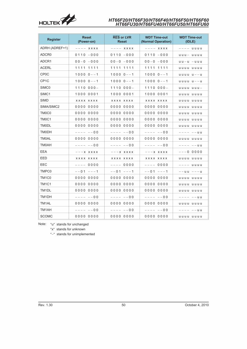
HT66F20/HT66F30/HT66F40/HT66F50/HT66F60HT66FU30/HT66FU40/HT66FU50/HT66FU60
Rev. 1.30 50 October 4, 2010
RegisterReset
(Power-on)
RES or LVR
Reset
WDT Time-out
(Normal Operation)
WDT Time-out
(IDLE)
ADRH (ADREF=1) � � � � x x x x � � � � x x x x � � � � x x x x � � � � u u u u
ADCR0 0 1 1 0 � 0 0 0 0 1 1 0 � 0 0 0 0 1 1 0 � 0 0 0 u u u � u u u u
ADCR1 0 0 � 0 � 0 0 0 0 0 � 0 � 0 0 0 0 0 � 0 � 0 0 0 u u � u � u u u
ACERL 1 1 1 1 1 1 1 1 1 1 1 1 1 1 1 1 1 1 1 1 1 1 1 1 u u u u u u u u
CP0C 1 0 0 0 0 � � 1 1 0 0 0 0 � � 1 1 0 0 0 0 � � 1 u u u u u � � u
CP1C 1 0 0 0 0 � � 1 1 0 0 0 0 � � 1 1 0 0 0 0 � � 1 u u u u u � � u
SIMC0 1 1 1 0 0 0 0 � 1 1 1 0 0 0 0 � 1 1 1 0 0 0 0 � u u u u u u u �
SIMC1 1 0 0 0 0 0 0 1 1 0 0 0 0 0 0 1 1 0 0 0 0 0 0 1 u u u u u u u u
SIMD x x x x x x x x x x x x x x x x x x x x x x x x u u u u u u u u
SIMA/SIMC2 0 0 0 0 0 0 0 0 0 0 0 0 0 0 0 0 0 0 0 0 0 0 0 0 u u u u u u u u
TM0C0 0 0 0 0 0 0 0 0 0 0 0 0 0 0 0 0 0 0 0 0 0 0 0 0 u u u u u u u u
TM0C1 0 0 0 0 0 0 0 0 0 0 0 0 0 0 0 0 0 0 0 0 0 0 0 0 u u u u u u u u
TM0DL 0 0 0 0 0 0 0 0 0 0 0 0 0 0 0 0 0 0 0 0 0 0 0 0 u u u u u u u u
TM0DH � � � � � � 0 0 � � � � � � 0 0 � � � � � � 0 0 � � � � � � u u
TM0AL 0 0 0 0 0 0 0 0 0 0 0 0 0 0 0 0 0 0 0 0 0 0 0 0 u u u u u u u u
TM0AH � � � � � � 0 0 � � � � � � 0 0 � � � � � � 0 0 � � � � � � u u
EEA � � � x x x x x � � � x x x x x � � � x x x x x � � � 0 0 0 0 0
EED x x x x x x x x x x x x x x x x x x x x x x x x u u u u u u u u
EEC � � � � 0 0 0 0 � � � � 0 0 0 0 � � � � 0 0 0 0 � � � � u u u u
TMPC0 � � 0 1 � � � 1 � � 0 1 � � � 1 � � 0 1 � � � 1 � � u u � � � u
TM1C0 0 0 0 0 0 0 0 0 0 0 0 0 0 0 0 0 0 0 0 0 0 0 0 0 u u u u u u u u
TM1C1 0 0 0 0 0 0 0 0 0 0 0 0 0 0 0 0 0 0 0 0 0 0 0 0 u u u u u u u u
TM1DL 0 0 0 0 0 0 0 0 0 0 0 0 0 0 0 0 0 0 0 0 0 0 0 0 u u u u u u u u
TM1DH � � � � � � 0 0 � � � � � � 0 0 � � � � � � 0 0 � � � � � � u u
TM1AL 0 0 0 0 0 0 0 0 0 0 0 0 0 0 0 0 0 0 0 0 0 0 0 0 u u u u u u u u
TM1AH � � � � � � 0 0 � � � � � � 0 0 � � � � � � 0 0 � � � � � � u u
SCOMC 0 0 0 0 0 0 0 0 0 0 0 0 0 0 0 0 0 0 0 0 0 0 0 0 u u u u u u u u
Note: �u� stands for unchanged
�x� stands for unknown
��� stands for unimplemented

HT66F20/HT66F30/HT66F40/HT66F50/HT66F60HT66FU30/HT66FU40/HT66FU50/HT66FU60
Rev. 1.30 51 October 4, 2010
� HT66F30 Register
RegisterReset
(Power-on)
RES or LVR
Reset
WDT Time-out
(Normal Operation)
WDT Time-out
(IDLE)
MP0 � x x x x x x x � x x x x x x x � x x x x x x x � u u u u u u u
MP1 � x x x x x x x � x x x x x x x � x x x x x x x � u u u u u u u
BP � � �� � � 0 0 � � �� � � 0 0 � � �� � � 0 0 � � �� � � u u
ACC x x x x x x x x u u u u u u u u u u u u u u u u u u u u u u u u
PCL 0 0 0 0 0 0 0 0 0 0 0 0 0 0 0 0 0 0 0 0 0 0 0 0 0 0 0 0 0 0 0 0
TBLP x x x x x x x x u u u u u u u u u u u u u u u u u u u u u u u u
TBLH � � x x x x x x � � u u u u u u � � u u u u u u � � u u u u u u
TBHP � �� � � x x x � �� � � u u u � �� � � u u u � �� � � u u u
STATUS � � 0 0 x x x x � � u u u u u u � � 1 u u u u u � � 1 1 u u u u
SMOD 0 0 0 0 0 0 1 1 0 0 0 0 0 0 1 1 0 0 0 0 0 0 1 1 u u u u u u u u
LVDC � � 0 0 � 0 0 0 � � 0 0 � 0 0 0 � � 0 0 � 0 0 0 � � u u � u u u
INTEG � �� � 0 0 0 0 � �� � 0 0 0 0 � �� � 0 0 0 0 � �� � u u u u
WDTC 0 1 1 1 1 0 1 0 0 1 1 1 1 0 1 0 0 1 1 1 1 0 1 0 u u u u u u u u
TBC 0 0 1 1 0 1 1 1 0 0 1 1 0 1 1 1 0 0 1 1 0 1 1 1 u u u u u u u u
INTC0 � 0 0 0 0 0 0 0 � 0 0 0 0 0 0 0 � 0 0 0 0 0 0 0 � u u u u u u u
INTC1 0 0 0 0 0 0 0 0 0 0 0 0 0 0 0 0 0 0 0 0 0 0 0 0 u u u u u u u u
INTC2 0 0 0 0 0 0 0 0 0 0 0 0 0 0 0 0 0 0 0 0 0 0 0 0 u u u u u u u u
MFI0 � � 0 0 � � 0 0 � � 0 0 � � 0 0 � � 0 0 � � 0 0 � � u u � � u u
MFI1 � 0 0 0 � 0 0 0 � 0 0 0 � 0 0 0 � 0 0 0 � 0 0 0 � u u u � u u u
MFI2 0 0 0 0 0 0 0 0 0 0 0 0 0 0 0 0 0 0 0 0 0 0 0 0 u u u u u u u u
PAWU 0 0 0 0 0 0 0 0 0 0 0 0 0 0 0 0 0 0 0 0 0 0 0 0 u u u u u u u u
PAPU 0 0 0 0 0 0 0 0 0 0 0 0 0 0 0 0 0 0 0 0 0 0 0 0 u u u u u u u u
PA 1 1 1 1 1 1 1 1 1 1 1 1 1 1 1 1 1 1 1 1 1 1 1 1 u u u u u u u u
PAC 1 1 1 1 1 1 1 1 1 1 1 1 1 1 1 1 1 1 1 1 1 1 1 1 u u u u u u u u
PBPU � � 0 0 0 0 0 0 � � 0 0 0 0 0 0 � � 0 0 0 0 0 0 � � u u u u u u
PB � � 1 1 1 1 1 1 � � 1 1 1 1 1 1 � � 1 1 1 1 1 1 � � u u u u u u
PBC � � 1 1 1 1 1 1 � � 1 1 1 1 1 1 � � 1 1 1 1 1 1 � � u u u u u u
PCPU 0 0 0 0 0 0 0 0 0 0 0 0 0 0 0 0 0 0 0 0 0 0 0 0 u u u u u u u u
PC 1 1 1 1 1 1 1 1 1 1 1 1 1 1 1 1 1 1 1 1 1 1 1 1 u u u u u u u u
PCC 1 1 1 1 1 1 1 1 1 1 1 1 1 1 1 1 1 1 1 1 1 1 1 1 u u u u u u u u
ADRL (ADREF=0) x x x x � � � � x x x x � � � � x x x x � � � � u u u u � � � �
ADRL (ADREF=1) x x x x x x x x x x x x x x x x x x x x x x x x u u u u u u u u
ADRH(ADREF=0) x x x x x x x x x x x x x x x x x x x x x x x x u u u u u u u u
ADRH (ADREF=1) � � � � x x x x � � � � x x x x � � � � x x x x � � � � u u u u
ADCR0 0 1 1 0 � 0 0 0 0 1 1 0 � 0 0 0 0 1 1 0 � 0 0 0 u u u u � u u u
ADCR1 0 0 � 0 � 0 0 0 0 0 � 0 � 0 0 0 0 0 � 0 � 0 0 0 u u � u � u u u
ACERL 1 1 1 1 1 1 1 1 1 1 1 1 1 1 1 1 1 1 1 1 1 1 1 1 u u u u u u u u
CP0C 1 0 0 0 0 � � 1 1 0 0 0 0 � � 1 1 0 0 0 0 � � 1 u u u u u � � u

HT66F20/HT66F30/HT66F40/HT66F50/HT66F60HT66FU30/HT66FU40/HT66FU50/HT66FU60
Rev. 1.30 52 October 4, 2010
RegisterReset
(Power-on)
RES or LVR
Reset
WDT Time-out
(Normal Operation)
WDT Time-out
(IDLE)
CP1C 1 0 0 0 0 � � 1 1 0 0 0 0 � � 1 1 0 0 0 0 � � 1 u u u u u � � u
SIMC0 1 1 1 0 0 0 0 � 1 1 1 0 0 0 0 � 1 1 1 0 0 0 0 � u u u u u u u �
SIMC1 1 0 0 0 0 0 0 1 1 0 0 0 0 0 0 1 1 0 0 0 0 0 0 1 u u u u u u u u
SIMD x x x x x x x x x x x x x x x x x x x x x x x x u u u u u u u u
SIMA/SIMC2 0 0 0 0 0 0 0 0 0 0 0 0 0 0 0 0 0 0 0 0 0 0 0 0 u u u u u u u u
TM0C0 0 0 0 0 0 0 0 0 0 0 0 0 0 0 0 0 0 0 0 0 0 0 0 0 u u u u u u u u
TM0C1 0 0 0 0 0 0 0 0 0 0 0 0 0 0 0 0 0 0 0 0 0 0 0 0 u u u u u u u u
TM0DL 0 0 0 0 0 0 0 0 0 0 0 0 0 0 0 0 0 0 0 0 0 0 0 0 u u u u u u u u
TM0DH � � � � � � 0 0 � � � � � � 0 0 � � � � � � 0 0 � � � � � � u u
TM0AL 0 0 0 0 0 0 0 0 0 0 0 0 0 0 0 0 0 0 0 0 0 0 0 0 u u u u u u u u
TM0AH � � � � � � 0 0 � � � � � � 0 0 � � � � � � 0 0 � � � � � � u u
EEA � � x x x x x x � � x x x x x x � � x x x x x x � � u u u u u u
EED x x x x x x x x x x x x x x x x x x x x x x x x u u u u u u u u
EEC � � � � 0 0 0 0 � � � � 0 0 0 0 � � � � 0 0 0 0 � � � � u u u u
TMPC0 1 � 0 1 � � 0 1 1 � 0 1 � � 0 1 1 � 0 1 � � 0 1 u � u u � � u u
PRM0 � � � � � 0 0 0 � � � � � 0 0 0 � � � � � 0 0 0 � � � � � u u u
TM1C0 0 0 0 0 0 0 0 0 0 0 0 0 0 0 0 0 0 0 0 0 0 0 0 0 u u u u u u u u
TM1C1 0 0 0 0 0 0 0 0 0 0 0 0 0 0 0 0 0 0 0 0 0 0 0 0 u u u u u u u u
TM1C2 0 0 0 0 0 0 0 0 0 0 0 0 0 0 0 0 0 0 0 0 0 0 0 0 u u u u u u u u
TM1DL 0 0 0 0 0 0 0 0 0 0 0 0 0 0 0 0 0 0 0 0 0 0 0 0 u u u u u u u u
TM1DH � � � � � � 0 0 � � � � � � 0 0 � � � � � � 0 0 � � � � � � u u
TM1AL 0 0 0 0 0 0 0 0 0 0 0 0 0 0 0 0 0 0 0 0 0 0 0 0 u u u u u u u u
TM1AH � � � � � � 0 0 � � � � � � 0 0 � � � � � � 0 0 � � � � � � u u
TM1BL 0 0 0 0 0 0 0 0 0 0 0 0 0 0 0 0 0 0 0 0 0 0 0 0 u u u u u u u u
TM1BH � � � � � � 0 0 � � � � � � 0 0 � � � � � � 0 0 � � � � � � u u
SCOMC 0 0 0 0 0 0 0 0 0 0 0 0 0 0 0 0 0 0 0 0 0 0 0 0 u u u u u u u u
Note: �u� stands for unchanged
�x� stands for unknown
��� stands for unimplemented

HT66F20/HT66F30/HT66F40/HT66F50/HT66F60HT66FU30/HT66FU40/HT66FU50/HT66FU60
Rev. 1.30 53 October 4, 2010
� HT66F40 Register
RegisterReset
(Power-on)
RES or LVR
Reset
WDT Time-out
(Normal Operation)
WDT Time-out
(IDLE)
MP0 x x x x x x x x x x x x x x x x x x x x x x x x u u u u u u u u
MP1 x x x x x x x x x x x x x x x x x x x x x x x x u u u u u u u u
BP � �� � � �� 0 � � �� � �� 0 � � �� � �� 0 � � �� � �� u
ACC x x x x x x x x u u u u u u u u u u u u u u u u u u u u u u u u
PCL 0 0 0 0 0 0 0 0 0 0 0 0 0 0 0 0 0 0 0 0 0 0 0 0 0 0 0 0 0 0 0 0
TBLP x x x x x x x x u u u u u u u u u u u u u u u u u u u u u u u u
TBLH � x x x x x x x � u u u u u u u � u u u u u u u � u u u u u u u
TBHP � �� � x x x x � �� � u u u u � �� � u u u u � �� � u u u u
STATUS � � 0 0 x x x x � � u u u u u u � � 1 u u u u u � � 1 1 u u u u
SMOD 0 0 0 0 0 0 1 1 0 0 0 0 0 0 1 1 0 0 0 0 0 0 1 1 u u u u u u u u
LVDC � � 0 0 � 0 0 0 � � 0 0 � 0 0 0 � � 0 0 � 0 0 0 � � u u � u u u
INTEG � �� � 0 0 0 0 � �� � 0 0 0 0 � �� � 0 0 0 0 � �� � u u u u
WDTC 0 1 1 1 1 0 1 0 0 1 1 1 1 0 1 0 0 1 1 1 1 0 1 0 u u u u u u u u
TBC 0 0 1 1 0 1 1 1 0 0 1 1 0 1 1 1 0 0 1 1 0 1 1 1 u u u u u u u u
INTC0 � 0 0 0 0 0 0 0 � 0 0 0 0 0 0 0 � 0 0 0 0 0 0 0 � u u u u u u u
INTC1 0 0 0 0 0 0 0 0 0 0 0 0 0 0 0 0 0 0 0 0 0 0 0 0 u u u u u u u u
INTC2 0 0 0 0 0 0 0 0 0 0 0 0 0 0 0 0 0 0 0 0 0 0 0 0 u u u u u u u u
MFI0 0 0 0 0 0 0 0 0 0 0 0 0 0 0 0 0 0 0 0 0 0 0 0 0 u u u u u u u u
MFI1 � 0 0 0 � 0 0 0 � 0 0 0 � 0 0 0 � 0 0 0 � 0 0 0 � u u u � u u u
MFI2 0 0 0 0 0 0 0 0 0 0 0 0 0 0 0 0 0 0 0 0 0 0 0 0 u u u u u u u u
PAWU 0 0 0 0 0 0 0 0 0 0 0 0 0 0 0 0 0 0 0 0 0 0 0 0 u u u u u u u u
PAPU 0 0 0 0 0 0 0 0 0 0 0 0 0 0 0 0 0 0 0 0 0 0 0 0 u u u u u u u u
PA 1 1 1 1 1 1 1 1 1 1 1 1 1 1 1 1 1 1 1 1 1 1 1 1 u u u u u u u u
PAC 1 1 1 1 1 1 1 1 1 1 1 1 1 1 1 1 1 1 1 1 1 1 1 1 u u u u u u u u
PBPU 0 0 0 0 0 0 0 0 0 0 0 0 0 0 0 0 0 0 0 0 0 0 0 0 u u u u u u u u
PB 1 1 1 1 1 1 1 1 1 1 1 1 1 1 1 1 1 1 1 1 1 1 1 1 u u u u u u u u
PBC 1 1 1 1 1 1 1 1 1 1 1 1 1 1 1 1 1 1 1 1 1 1 1 1 u u u u u u u u
PCPU 0 0 0 0 0 0 0 0 0 0 0 0 0 0 0 0 0 0 0 0 0 0 0 0 u u u u u u u u
PC 1 1 1 1 1 1 1 1 1 1 1 1 1 1 1 1 1 1 1 1 1 1 1 1 u u u u u u u u
PCC 1 1 1 1 1 1 1 1 1 1 1 1 1 1 1 1 1 1 1 1 1 1 1 1 u u u u u u u u
PDPU 0 0 0 0 0 0 0 0 0 0 0 0 0 0 0 0 0 0 0 0 0 0 0 0 u u u u u u u u
PD 1 1 1 1 1 1 1 1 1 1 1 1 1 1 1 1 1 1 1 1 1 1 1 1 u u u u u u u u
PDC 1 1 1 1 1 1 1 1 1 1 1 1 1 1 1 1 1 1 1 1 1 1 1 1 u u u u u u u u
PEPU 0 0 0 0 0 0 0 0 0 0 0 0 0 0 0 0 0 0 0 0 0 0 0 0 u u u u u u u u
PE 1 1 1 1 1 1 1 1 1 1 1 1 1 1 1 1 1 1 1 1 1 1 1 1 u u u u u u u u
PEC 1 1 1 1 1 1 1 1 1 1 1 1 1 1 1 1 1 1 1 1 1 1 1 1 u u u u u u u u
PFPU � �� � � � 0 0 � �� � � � 0 0 � �� � � � 0 0 � �� � � � u u
PF � �� � � � 1 1 � �� � � � 1 1 � �� � � � 1 1 � �� � � � u u
PFC � �� � � � 1 1 � �� � � � 1 1 � �� � � � 1 1 � �� � � � u u
ADRL (ADREF=0) x x x x � � � � x x x x � � � � x x x x � � � � u u u u � � � �
ADRL (ADREF=1) x x x x x x x x x x x x x x x x x x x x x x x x u u u u u u u u
ADRH(ADREF=0) x x x x x x x x x x x x x x x x x x x x x x x x u u u u u u u u
ADRH (ADREF=1) � � � � x x x x � � � � x x x x � � � � x x x x � � � � u u u u

HT66F20/HT66F30/HT66F40/HT66F50/HT66F60HT66FU30/HT66FU40/HT66FU50/HT66FU60
Rev. 1.30 54 October 4, 2010
RegisterReset
(Power-on)
RES or LVR
Reset
WDT Time-out
(Normal Operation)
WDT Time-out
(IDLE)
ADCR0 0 1 1 0 � 0 0 0 0 1 1 0 � 0 0 0 0 1 1 0 � 0 0 0 u u u u � u u u
ADCR1 0 0 � 0 � 0 0 0 0 0 � 0 � 0 0 0 0 0 � 0 � 0 0 0 u u � u � u u u
ACERL 1 1 1 1 1 1 1 1 1 1 1 1 1 1 1 1 1 1 1 1 1 1 1 1 u u u u u u u u
CP0C 1 0 0 0 0 � � 1 1 0 0 0 0 � � 1 1 0 0 0 0 � � 1 u u u u u � � u
CP1C 1 0 0 0 0 � � 1 1 0 0 0 0 � � 1 1 0 0 0 0 � � 1 u u u u u � � u
SIMC0 1 1 1 0 0 0 0 � 1 1 1 0 0 0 0 � 1 1 1 0 0 0 0 � u u u u u u u �
SIMC1 1 0 0 0 0 0 0 1 1 0 0 0 0 0 0 1 1 0 0 0 0 0 0 1 u u u u u u u u
SIMD x x x x x x x x x x x x x x x x x x x x x x x x u u u u u u u u
SIMA/SIMC2 0 0 0 0 0 0 0 0 0 0 0 0 0 0 0 0 0 0 0 0 0 0 0 0 u u u u u u u u
TM0C0 0 0 0 0 0 0 0 0 0 0 0 0 0 0 0 0 0 0 0 0 0 0 0 0 u u u u u u u u
TM0C1 0 0 0 0 0 0 0 0 0 0 0 0 0 0 0 0 0 0 0 0 0 0 0 0 u u u u u u u u
TM0DL 0 0 0 0 0 0 0 0 0 0 0 0 0 0 0 0 0 0 0 0 0 0 0 0 u u u u u u u u
TM0DH � � � � � � 0 0 � � � � � � 0 0 � � � � � � 0 0 � � � � � � u u
TM0AL 0 0 0 0 0 0 0 0 0 0 0 0 0 0 0 0 0 0 0 0 0 0 0 0 u u u u u u u u
TM0AH � � � � � � 0 0 � � � � � � 0 0 � � � � � � 0 0 � � � � � � u u
EEA � x x x x x x x � x x x x x x x � x x x x x x x � u u u u u u u
EED x x x x x x x x x x x x x x x x x x x x x x x x u u u u u u u u
EEC � � � � 0 0 0 0 � � � � 0 0 0 0 � � � � 0 0 0 0 � � � � u u u u
TMPC0 1 0 0 1 � � 0 1 1 0 0 1 � � 0 1 1 0 0 1 � � 0 1 u u u u � � u u
TMPC1 � � � � � � 0 1 � � � � � � 0 1 � � � � � � 0 1 � � � � � � u u
PRM0 � 0 � 0 0 0 0 0 � 0 � 0 0 0 0 0 � 0 � 0 0 0 0 0 � u � u u u u u
PRM1 0 0 0 � 0 0 0 0 0 0 0 � 0 0 0 0 0 0 0 � 0 0 0 0 u u u � u u u u
PRM2 � � 0 0 0 0 0 0 � � 0 0 0 0 0 0 � � 0 0 0 0 0 0 � � u u u u u u
TM1C0 0 0 0 0 0 0 0 0 0 0 0 0 0 0 0 0 0 0 0 0 0 0 0 0 u u u u u u u u
TM1C1 0 0 0 0 0 0 0 0 0 0 0 0 0 0 0 0 0 0 0 0 0 0 0 0 u u u u u u u u
TM1C2 0 0 0 0 0 0 0 0 0 0 0 0 0 0 0 0 0 0 0 0 0 0 0 0 u u u u u u u u
TM1DL 0 0 0 0 0 0 0 0 0 0 0 0 0 0 0 0 0 0 0 0 0 0 0 0 u u u u u u u u
TM1DH � � � � � � 0 0 � � � � � � 0 0 � � � � � � 0 0 � � � � � � u u
TM1AL 0 0 0 0 0 0 0 0 0 0 0 0 0 0 0 0 0 0 0 0 0 0 0 0 u u u u u u u u
TM1AH � � � � � � 0 0 � � � � � � 0 0 � � � � � � 0 0 � � � � � � u u
TM1BL 0 0 0 0 0 0 0 0 0 0 0 0 0 0 0 0 0 0 0 0 0 0 0 0 u u u u u u u u
TM1BH � � � � � � 0 0 � � � � � � 0 0 � � � � � � 0 0 � � � � � � u u
TM2C0 0 0 0 0 0 � � � 0 0 0 0 0 � � � 0 0 0 0 0 � � � u u u u u � � �
TM2C1 0 0 0 0 0 0 0 0 0 0 0 0 0 0 0 0 0 0 0 0 0 0 0 0 u u u u u u u u
TM2DL 0 0 0 0 0 0 0 0 0 0 0 0 0 0 0 0 0 0 0 0 0 0 0 0 u u u u u u u u
TM2DH 0 0 0 0 0 0 0 0 0 0 0 0 0 0 0 0 0 0 0 0 0 0 0 0 u u u u u u u u
TM2AL 0 0 0 0 0 0 0 0 0 0 0 0 0 0 0 0 0 0 0 0 0 0 0 0 u u u u u u u u
TM2AH 0 0 0 0 0 0 0 0 0 0 0 0 0 0 0 0 0 0 0 0 0 0 0 0 u u u u u u u u
TM2RP 0 0 0 0 0 0 0 0 0 0 0 0 0 0 0 0 0 0 0 0 0 0 0 0 u u u u u u u u
SCOMC 0 0 0 0 0 0 0 0 0 0 0 0 0 0 0 0 0 0 0 0 0 0 0 0 u u u u u u u u
Note: �u� stands for unchanged
�x� stands for unknown
��� stands for unimplemented

HT66F20/HT66F30/HT66F40/HT66F50/HT66F60HT66FU30/HT66FU40/HT66FU50/HT66FU60
Rev. 1.30 55 October 4, 2010
� HT66F50 Register
RegisterReset
(Power-on)
RES or LVR
Reset
WDT Time-out
(Normal Operation)
WDT Time-out
(IDLE)
MP0 x x x x x x x x x x x x x x x x x x x x x x x x u u u u u u u u
MP1 x x x x x x x x x x x x x x x x x x x x x x x x u u u u u u u u
BP � �� � � � 0 0 � �� � � � 0 0 � �� � � � 0 0 � �� � � � u u
ACC x x x x x x x x u u u u u u u u u u u u u u u u u u u u u u u u
PCL 0 0 0 0 0 0 0 0 0 0 0 0 0 0 0 0 0 0 0 0 0 0 0 0 0 0 0 0 0 0 0 0
TBLP x x x x x x x x u u u u u u u u u u u u u u u u u u u u u u u u
TBLH x x x x x x x x u u u u u u u u u u u u u u u u u u u u u u u u
TBHP � �� x x x x x � �� u u u u u � �� u u u u u � �� u u u u u
STATUS � � 0 0 x x x x � � u u u u u u � � 1 u u u u u � � 1 1 u u u u
SMOD 0 0 0 0 0 0 1 1 0 0 0 0 0 0 1 1 0 0 0 0 0 0 1 1 u u u u u u u u
LVDC � � 0 0 � 0 0 0 � � 0 0 � 0 0 0 � � 0 0 � 0 0 0 � � u u � u u u
INTEG � �� � 0 0 0 0 � �� � 0 0 0 0 � �� � 0 0 0 0 � �� � u u u u
WDTC 0 1 1 1 1 0 1 0 0 1 1 1 1 0 1 0 0 1 1 1 1 0 1 0 u u u u u u u u
TBC 0 0 1 1 0 1 1 1 0 0 1 1 0 1 1 1 0 0 1 1 0 1 1 1 u u u u u u u u
INTC0 � 0 0 0 0 0 0 0 � 0 0 0 0 0 0 0 � 0 0 0 0 0 0 0 � u u u u u u u
INTC1 0 0 0 0 0 0 0 0 0 0 0 0 0 0 0 0 0 0 0 0 0 0 0 0 u u u u u u u u
INTC2 0 0 0 0 0 0 0 0 0 0 0 0 0 0 0 0 0 0 0 0 0 0 0 0 u u u u u u u u
MFI0 0 0 0 0 0 0 0 0 0 0 0 0 0 0 0 0 0 0 0 0 0 0 0 0 u u u u u u u u
MFI1 � 0 0 0 � 0 0 0 � 0 0 0 � 0 0 0 � 0 0 0 � 0 0 0 � u u u � u u u
MFI2 0 0 0 0 0 0 0 0 0 0 0 0 0 0 0 0 0 0 0 0 0 0 0 0 u u u u u u u u
MFI3 � � 0 0 � � 0 0 � � 0 0 � � 0 0 � � 0 0 � � 0 0 � � u u � � u u
PAWU 0 0 0 0 0 0 0 0 0 0 0 0 0 0 0 0 0 0 0 0 0 0 0 0 u u u u u u u u
PAPU 0 0 0 0 0 0 0 0 0 0 0 0 0 0 0 0 0 0 0 0 0 0 0 0 u u u u u u u u
PA 1 1 1 1 1 1 1 1 1 1 1 1 1 1 1 1 1 1 1 1 1 1 1 1 u u u u u u u u
PAC 1 1 1 1 1 1 1 1 1 1 1 1 1 1 1 1 1 1 1 1 1 1 1 1 u u u u u u u u
PBPU 0 0 0 0 0 0 0 0 0 0 0 0 0 0 0 0 0 0 0 0 0 0 0 0 u u u u u u u u
PB 1 1 1 1 1 1 1 1 1 1 1 1 1 1 1 1 1 1 1 1 1 1 1 1 u u u u u u u u
PBC 1 1 1 1 1 1 1 1 1 1 1 1 1 1 1 1 1 1 1 1 1 1 1 1 u u u u u u u u
PCPU 0 0 0 0 0 0 0 0 0 0 0 0 0 0 0 0 0 0 0 0 0 0 0 0 u u u u u u u u
PC 1 1 1 1 1 1 1 1 1 1 1 1 1 1 1 1 1 1 1 1 1 1 1 1 u u u u u u u u
PCC 1 1 1 1 1 1 1 1 1 1 1 1 1 1 1 1 1 1 1 1 1 1 1 1 u u u u u u u u
PDPU 0 0 0 0 0 0 0 0 0 0 0 0 0 0 0 0 0 0 0 0 0 0 0 0 u u u u u u u u
PD 1 1 1 1 1 1 1 1 1 1 1 1 1 1 1 1 1 1 1 1 1 1 1 1 u u u u u u u u
PDC 1 1 1 1 1 1 1 1 1 1 1 1 1 1 1 1 1 1 1 1 1 1 1 1 u u u u u u u u
PEPU 0 0 0 0 0 0 0 0 0 0 0 0 0 0 0 0 0 0 0 0 0 0 0 0 u u u u u u u u
PE 1 1 1 1 1 1 1 1 1 1 1 1 1 1 1 1 1 1 1 1 1 1 1 1 u u u u u u u u
PEC 1 1 1 1 1 1 1 1 1 1 1 1 1 1 1 1 1 1 1 1 1 1 1 1 u u u u u u u u
PFPU � �� � � � 0 0 � �� � � � 0 0 � �� � � � 0 0 � �� � � � u u

HT66F20/HT66F30/HT66F40/HT66F50/HT66F60HT66FU30/HT66FU40/HT66FU50/HT66FU60
Rev. 1.30 56 October 4, 2010
RegisterReset
(Power-on)
RES or LVR
Reset
WDT Time-out
(Normal Operation)
WDT Time-out
(IDLE)
PF � �� � � � 1 1 � �� � � � 1 1 � �� � � � 1 1 � �� � � � u u
PFC � �� � � � 1 1 � �� � � � 1 1 � �� � � � 1 1 � �� � � � u u
ADRL (ADREF=0) x x x x � � � � x x x x � � � � x x x x � � � � u u u u � � � �
ADRL (ADREF=1) x x x x x x x x x x x x x x x x x x x x x x x x u u u u u u u u
ADRH(ADREF=0) x x x x x x x x x x x x x x x x x x x x x x x x u u u u u u u u
ADRH (ADREF=1) � � � � x x x x � � � � x x x x � � � � x x x x � � � � u u u u
ADCR0 0 1 1 0 � 0 0 0 0 1 1 0 � 0 0 0 0 1 1 0 � 0 0 0 u u u u � u u u
ADCR1 0 0 � 0 � 0 0 0 0 0 � 0 � 0 0 0 0 0 � 0 � 0 0 0 u u � u � u u u
ACERL 1 1 1 1 1 1 1 1 1 1 1 1 1 1 1 1 1 1 1 1 1 1 1 1 u u u u u u u u
CP0C 1 0 0 0 0 � � 1 1 0 0 0 0 � � 1 1 0 0 0 0 � � 1 u u u u u � � u
CP1C 1 0 0 0 0 � � 1 1 0 0 0 0 � � 1 1 0 0 0 0 � � 1 u u u u u � � u
SIMC0 1 1 1 0 0 0 0 � 1 1 1 0 0 0 0 � 1 1 1 0 0 0 0 � u u u u u u u �
SIMC1 1 0 0 0 0 0 0 1 1 0 0 0 0 0 0 1 1 0 0 0 0 0 0 1 u u u u u u u u
SIMD x x x x x x x x x x x x x x x x x x x x x x x x u u u u u u u u
SIMA/SIMC2 0 0 0 0 0 0 0 0 0 0 0 0 0 0 0 0 0 0 0 0 0 0 0 0 u u u u u u u u
TM0C0 0 0 0 0 0 0 0 0 0 0 0 0 0 0 0 0 0 0 0 0 0 0 0 0 u u u u u u u u
TM0C1 0 0 0 0 0 0 0 0 0 0 0 0 0 0 0 0 0 0 0 0 0 0 0 0 u u u u u u u u
TM0DL 0 0 0 0 0 0 0 0 0 0 0 0 0 0 0 0 0 0 0 0 0 0 0 0 u u u u u u u u
TM0DH � � � � � � 0 0 � � � � � � 0 0 � � � � � � 0 0 � � � � � � u u
TM0AL 0 0 0 0 0 0 0 0 0 0 0 0 0 0 0 0 0 0 0 0 0 0 0 0 u u u u u u u u
TM0AH � � � � � � 0 0 � � � � � � 0 0 � � � � � � 0 0 � � � � � � u u
EEA x x x x x x x x x x x x x x x x x x x x x x x x u u u u u u u u
EED x x x x x x x x x x x x x x x x x x x x x x x x u u u u u u u u
EEC � � � � 0 0 0 0 � � � � 0 0 0 0 � � � � 0 0 0 0 � � � � u u u u
TMPC0 1 0 0 1 � � 0 1 1 0 0 1 � � 0 1 1 0 0 1 � � 0 1 u u u u � � u u
TMPC1 � � 0 1 � � 0 1 � � 0 1 � � 0 1 � � 0 1 � � 0 1 � � u u � � u u
PRM0 � 0 � 0 0 0 0 0 � 0 � 0 0 0 0 0 � 0 � 0 0 0 0 0 � u � u u u u u
PRM1 0 0 0 � 0 0 0 0 0 0 0 � 0 0 0 0 0 0 0 � 0 0 0 0 u u u � u u u u
PRM2 0 0 0 0 0 0 0 0 0 0 0 0 0 0 0 0 0 0 0 0 0 0 0 0 u u u u u u u u
TM1C0 0 0 0 0 0 0 0 0 0 0 0 0 0 0 0 0 0 0 0 0 0 0 0 0 u u u u u u u u
TM1C1 0 0 0 0 0 0 0 0 0 0 0 0 0 0 0 0 0 0 0 0 0 0 0 0 u u u u u u u u
TM1C2 0 0 0 0 0 0 0 0 0 0 0 0 0 0 0 0 0 0 0 0 0 0 0 0 u u u u u u u u
TM1DL 0 0 0 0 0 0 0 0 0 0 0 0 0 0 0 0 0 0 0 0 0 0 0 0 u u u u u u u u
TM1DH � � � � � � 0 0 � � � � � � 0 0 � � � � � � 0 0 � � � � � � u u
TM1AL 0 0 0 0 0 0 0 0 0 0 0 0 0 0 0 0 0 0 0 0 0 0 0 0 u u u u u u u u
TM1AH � � � � � � 0 0 � � � � � � 0 0 � � � � � � 0 0 � � � � � � u u
TM1BL 0 0 0 0 0 0 0 0 0 0 0 0 0 0 0 0 0 0 0 0 0 0 0 0 u u u u u u u u
TM1BH � � � � � � 0 0 � � � � � � 0 0 � � � � � � 0 0 � � � � � � u u

HT66F20/HT66F30/HT66F40/HT66F50/HT66F60HT66FU30/HT66FU40/HT66FU50/HT66FU60
Rev. 1.30 57 October 4, 2010
RegisterReset
(Power-on)
RES or LVR
Reset
WDT Time-out
(Normal Operation)
WDT Time-out
(IDLE)
TM2C0 0 0 0 0 0 � � � 0 0 0 0 0 � � � 0 0 0 0 0 � � � u u u u u � � �
TM2C1 0 0 0 0 0 0 0 0 0 0 0 0 0 0 0 0 0 0 0 0 0 0 0 0 u u u u u u u u
TM2DL 0 0 0 0 0 0 0 0 0 0 0 0 0 0 0 0 0 0 0 0 0 0 0 0 u u u u u u u u
TM2DH 0 0 0 0 0 0 0 0 0 0 0 0 0 0 0 0 0 0 0 0 0 0 0 0 u u u u u u u u
TM2AL 0 0 0 0 0 0 0 0 0 0 0 0 0 0 0 0 0 0 0 0 0 0 0 0 u u u u u u u u
TM2AH 0 0 0 0 0 0 0 0 0 0 0 0 0 0 0 0 0 0 0 0 0 0 0 0 u u u u u u u u
TM2RP 0 0 0 0 0 0 0 0 0 0 0 0 0 0 0 0 0 0 0 0 0 0 0 0 u u u u u u u u
TM3C0 0 0 0 0 0 0 0 0 0 0 0 0 0 0 0 0 0 0 0 0 0 0 0 0 u u u u u u u u
TM3C1 0 0 0 0 0 0 0 0 0 0 0 0 0 0 0 0 0 0 0 0 0 0 0 0 u u u u u u u u
TM3DL 0 0 0 0 0 0 0 0 0 0 0 0 0 0 0 0 0 0 0 0 0 0 0 0 u u u u u u u u
TM3DH � � � � � � 0 0 � � � � � � 0 0 � � � � � � 0 0 � � � � � � u u
TM3AL 0 0 0 0 0 0 0 0 0 0 0 0 0 0 0 0 0 0 0 0 0 0 0 0 u u u u u u u u
TM3AH � � � � � � 0 0 � � � � � � 0 0 � � � � � � 0 0 � � � � � � u u
SCOMC 0 0 0 0 0 0 0 0 0 0 0 0 0 0 0 0 0 0 0 0 0 0 0 0 u u u u u u u u
Note: �u� stands for unchanged
�x� stands for unknown
��� stands for unimplemented

HT66F20/HT66F30/HT66F40/HT66F50/HT66F60HT66FU30/HT66FU40/HT66FU50/HT66FU60
Rev. 1.30 58 October 4, 2010
� HT66F60 Register
RegisterReset
(Power-on)
RES or LVR
Reset
WDT Time-out
(Normal Operation)
WDT Time-out
(IDLE)
MP0 x x x x x x x x x x x x x x x x x x x x x x x x u u u u u u u u
MP1 x x x x x x x x x x x x x x x x x x x x x x x x u u u u u u u u
BP � � 0� � 0 0 0 � � 0� � 0 0 0 � � 0� � 0 0 0 � � u � � u u u
ACC x x x x x x x x u u u u u u u u u u u u u u u u u u u u u u u u
PCL 0 0 0 0 0 0 0 0 0 0 0 0 0 0 0 0 0 0 0 0 0 0 0 0 0 0 0 0 0 0 0 0
TBLP x x x x x x x x u u u u u u u u u u u u u u u u u u u u u u u u
TBLH x x x x x x x x u u u u u u u u u u u u u u u u u u u u u u u u
TBHP � � x x x x x x � � u u u u u u � � u u u u u u � � u u u u u u
STATUS � � 0 0 x x x x � � u u u u u u � � 1 u u u u u � � 1 1 u u u u
SMOD 0 0 0 0 0 0 1 1 0 0 0 0 0 0 1 1 0 0 0 0 0 0 1 1 u u u u u u u u
LVDC � � 0 0 � 0 0 0 � � 0 0 � 0 0 0 � � 0 0 � 0 0 0 � � u u � u u u
INTEG 0 0 0 0 0 0 0 0 0 0 0 0 0 0 0 0 0 0 0 0 0 0 0 0 u u u u u u u u
WDTC 0 1 1 1 1 0 1 0 0 1 1 1 1 0 1 0 0 1 1 1 1 0 1 0 u u u u u u u u
TBC 0 0 1 1 0 1 1 1 0 0 1 1 0 1 1 1 0 0 1 1 0 1 1 1 u u u u u u u u
INTC0 � 0 0 0 0 0 0 0 � 0 0 0 0 0 0 0 � 0 0 0 0 0 0 0 � u u u u u u u
INTC1 0 0 0 0 0 0 0 0 0 0 0 0 0 0 0 0 0 0 0 0 0 0 0 0 u u u u u u u u
INTC2 0 0 0 0 0 0 0 0 0 0 0 0 0 0 0 0 0 0 0 0 0 0 0 0 u u u u u u u u
INTC3 0 0 0 0 0 0 0 0 0 0 0 0 0 0 0 0 0 0 0 0 0 0 0 0 u u u u u u u u
MFI0 0 0 0 0 0 0 0 0 0 0 0 0 0 0 0 0 0 0 0 0 0 0 0 0 u u u u u u u u
MFI1 � 0 0 0 � 0 0 0 � 0 0 0 � 0 0 0 � 0 0 0 � 0 0 0 � u u u � u u u
MFI2 0 0 0 0 0 0 0 0 0 0 0 0 0 0 0 0 0 0 0 0 0 0 0 0 u u u u u u u u
MFI3 � � 0 0 � � 0 0 � � 0 0 � � 0 0 � � 0 0 � � 0 0 � � u u � � u u
PAWU 0 0 0 0 0 0 0 0 0 0 0 0 0 0 0 0 0 0 0 0 0 0 0 0 u u u u u u u u
PAPU 0 0 0 0 0 0 0 0 0 0 0 0 0 0 0 0 0 0 0 0 0 0 0 0 u u u u u u u u
PA 1 1 1 1 1 1 1 1 1 1 1 1 1 1 1 1 1 1 1 1 1 1 1 1 u u u u u u u u
PAC 1 1 1 1 1 1 1 1 1 1 1 1 1 1 1 1 1 1 1 1 1 1 1 1 u u u u u u u u
PBPU 0 0 0 0 0 0 0 0 0 0 0 0 0 0 0 0 0 0 0 0 0 0 0 0 u u u u u u u u
PB 1 1 1 1 1 1 1 1 1 1 1 1 1 1 1 1 1 1 1 1 1 1 1 1 u u u u u u u u
PBC 1 1 1 1 1 1 1 1 1 1 1 1 1 1 1 1 1 1 1 1 1 1 1 1 u u u u u u u u
PCPU 0 0 0 0 0 0 0 0 0 0 0 0 0 0 0 0 0 0 0 0 0 0 0 0 u u u u u u u u
PC 1 1 1 1 1 1 1 1 1 1 1 1 1 1 1 1 1 1 1 1 1 1 1 1 u u u u u u u u
PCC 1 1 1 1 1 1 1 1 1 1 1 1 1 1 1 1 1 1 1 1 1 1 1 1 u u u u u u u u
PDPU 0 0 0 0 0 0 0 0 0 0 0 0 0 0 0 0 0 0 0 0 0 0 0 0 u u u u u u u u
PD 1 1 1 1 1 1 1 1 1 1 1 1 1 1 1 1 1 1 1 1 1 1 1 1 u u u u u u u u
PDC 1 1 1 1 1 1 1 1 1 1 1 1 1 1 1 1 1 1 1 1 1 1 1 1 u u u u u u u u
PEPU 0 0 0 0 0 0 0 0 0 0 0 0 0 0 0 0 0 0 0 0 0 0 0 0 u u u u u u u u
PE 1 1 1 1 1 1 1 1 1 1 1 1 1 1 1 1 1 1 1 1 1 1 1 1 u u u u u u u u
PEC 1 1 1 1 1 1 1 1 1 1 1 1 1 1 1 1 1 1 1 1 1 1 1 1 u u u u u u u u
PFPU 0 0 0 0 0 0 0 0 0 0 0 0 0 0 0 0 0 0 0 0 0 0 0 0 u u u u u u u u

HT66F20/HT66F30/HT66F40/HT66F50/HT66F60HT66FU30/HT66FU40/HT66FU50/HT66FU60
Rev. 1.30 59 October 4, 2010
RegisterReset
(Power-on)
RES or LVR
Reset
WDT Time-out
(Normal Operation)
WDT Time-out
(IDLE)
PF 1 1 1 1 1 1 1 1 1 1 1 1 1 1 1 1 1 1 1 1 1 1 1 1 u u u u u u u u
PFC 1 1 1 1 1 1 1 1 1 1 1 1 1 1 1 1 1 1 1 1 1 1 1 1 u u u u u u u u
PGPU � �� � � � 0 0 0 0 0 0 0 0 0 0 0 0 0 0 0 0 0 0 u u u u u u u u
PG � �� � � � 1 1 � �� � � � 1 1 � �� � � � 1 1 � �� � � � u u
PGC � �� � � � 1 1 � �� � � � 1 1 � �� � � � 1 1 � �� � � � u u
ADRL (ADREF=0) x x x x � � � � x x x x � � � � x x x x � � � � u u u u � � � �
ADRL (ADREF=1) x x x x x x x x x x x x x x x x x x x x x x x x u u u u u u u u
ADRH(ADREF=0) x x x x x x x x x x x x x x x x x x x x x x x x u u u u u u u u
ADRH (ADREF=1) � � � � x x x x � � � � x x x x � � � � x x x x � � � � u u u u
ADCR0 0 1 1 0 0 0 0 0 0 1 1 0 0 0 0 0 0 1 1 0 0 0 0 0 u u u u u u u u
ADCR1 0 0 � 0 � 0 0 0 0 0 � 0 � 0 0 0 0 0 � 0 � 0 0 0 u u � u � u u u
ACERL 1 1 1 1 1 1 1 1 1 1 1 1 1 1 1 1 1 1 1 1 1 1 1 1 u u u u u u u u
ACERH � �� � 1 1 1 1 � �� � 1 1 1 1 � �� � 1 1 1 1 � �� � u u u u
CP0C 1 0 0 0 0 � � 1 1 0 0 0 0 � � 1 1 0 0 0 0 � � 1 u u u u u � � u
CP1C 1 0 0 0 0 � � 1 1 0 0 0 0 � � 1 1 0 0 0 0 � � 1 u u u u u � � u
SIMC0 1 1 1 0 0 0 0 � 1 1 1 0 0 0 0 � 1 1 1 0 0 0 0 � u u u u u u u �
SIMC1 1 0 0 0 0 0 0 1 1 0 0 0 0 0 0 1 1 0 0 0 0 0 0 1 u u u u u u u u
SIMD x x x x x x x x x x x x x x x x x x x x x x x x u u u u u u u u
SIMA/SIMC2 0 0 0 0 0 0 0 0 0 0 0 0 0 0 0 0 0 0 0 0 0 0 0 0 u u u u u u u u
TM0C0 0 0 0 0 0 0 0 0 0 0 0 0 0 0 0 0 0 0 0 0 0 0 0 0 u u u u u u u u
TM0C1 0 0 0 0 0 0 0 0 0 0 0 0 0 0 0 0 0 0 0 0 0 0 0 0 u u u u u u u u
TM0DL 0 0 0 0 0 0 0 0 0 0 0 0 0 0 0 0 0 0 0 0 0 0 0 0 u u u u u u u u
TM0DH � � � � � � 0 0 � � � � � � 0 0 � � � � � � 0 0 � � � � � � u u
TM0AL 0 0 0 0 0 0 0 0 0 0 0 0 0 0 0 0 0 0 0 0 0 0 0 0 u u u u u u u u
TM0AH � � � � � � 0 0 � � � � � � 0 0 � � � � � � 0 0 � � � � � � u u
EEA x x x x x x x x x x x x x x x x x x x x x x x x u u u u u u u u
EED x x x x x x x x x x x x x x x x x x x x x x x x u u u u u u u u
EEC � � � � 0 0 0 0 � � � � 0 0 0 0 � � � � 0 0 0 0 � � � � u u u u
TMPC0 1 0 0 1 � � 0 1 1 0 0 1 � � 0 1 1 0 0 1 � � 0 1 u u u u � � u u
TMPC1 � � 0 1 � � 0 1 � � 0 1 � � 0 1 � � 0 1 � � 0 1 � � u u � � u u
PRM0 0 0 0 0 0 0 0 0 0 0 0 0 0 0 0 0 0 0 0 0 0 0 0 0 u u u u u u u u
PRM1 0 0 0 0 0 0 0 0 0 0 0 0 0 0 0 0 0 0 0 0 0 0 0 0 u u u u u u u u
PRM2 0 0 0 0 0 0 0 0 0 0 0 0 0 0 0 0 0 0 0 0 0 0 0 0 u u u u u u u u
TM1C0 0 0 0 0 0 0 0 0 0 0 0 0 0 0 0 0 0 0 0 0 0 0 0 0 u u u u u u u u
TM1C1 0 0 0 0 0 0 0 0 0 0 0 0 0 0 0 0 0 0 0 0 0 0 0 0 u u u u u u u u
TM1C2 0 0 0 0 0 0 0 0 0 0 0 0 0 0 0 0 0 0 0 0 0 0 0 0 u u u u u u u u
TM1DL 0 0 0 0 0 0 0 0 0 0 0 0 0 0 0 0 0 0 0 0 0 0 0 0 u u u u u u u u
TM1DH � � � � � � 0 0 � � � � � � 0 0 � � � � � � 0 0 � � � � � � u u
TM1AL 0 0 0 0 0 0 0 0 0 0 0 0 0 0 0 0 0 0 0 0 0 0 0 0 u u u u u u u u

HT66F20/HT66F30/HT66F40/HT66F50/HT66F60HT66FU30/HT66FU40/HT66FU50/HT66FU60
Rev. 1.30 60 October 4, 2010
RegisterReset
(Power-on)
RES or LVR
Reset
WDT Time-out
(Normal Operation)
WDT Time-out
(IDLE)
TM1AH � � � � � � 0 0 � � � � � � 0 0 � � � � � � 0 0 � � � � � � u u
TM1BL 0 0 0 0 0 0 0 0 0 0 0 0 0 0 0 0 0 0 0 0 0 0 0 0 u u u u u u u u
TM1BH � � � � � � 0 0 � � � � � � 0 0 � � � � � � 0 0 � � � � � � u u
TM2C0 0 0 0 0 0 � � � 0 0 0 0 0 � � � 0 0 0 0 0 � � � u u u u u � � �
TM2C1 0 0 0 0 0 0 0 0 0 0 0 0 0 0 0 0 0 0 0 0 0 0 0 0 u u u u u u u u
TM2DL 0 0 0 0 0 0 0 0 0 0 0 0 0 0 0 0 0 0 0 0 0 0 0 0 u u u u u u u u
TM2DH 0 0 0 0 0 0 0 0 0 0 0 0 0 0 0 0 0 0 0 0 0 0 0 0 u u u u u u u u
TM2AL 0 0 0 0 0 0 0 0 0 0 0 0 0 0 0 0 0 0 0 0 0 0 0 0 u u u u u u u u
TM2AH 0 0 0 0 0 0 0 0 0 0 0 0 0 0 0 0 0 0 0 0 0 0 0 0 u u u u u u u u
TM2RP 0 0 0 0 0 0 0 0 0 0 0 0 0 0 0 0 0 0 0 0 0 0 0 0 u u u u u u u u
TM3C0 0 0 0 0 0 0 0 0 0 0 0 0 0 0 0 0 0 0 0 0 0 0 0 0 u u u u u u u u
TM3C1 0 0 0 0 0 0 0 0 0 0 0 0 0 0 0 0 0 0 0 0 0 0 0 0 u u u u u u u u
TM3DL 0 0 0 0 0 0 0 0 0 0 0 0 0 0 0 0 0 0 0 0 0 0 0 0 u u u u u u u u
TM3DH � � � � � � 0 0 � � � � � � 0 0 � � � � � � 0 0 � � � � � � u u
TM3AL 0 0 0 0 0 0 0 0 0 0 0 0 0 0 0 0 0 0 0 0 0 0 0 0 u u u u u u u u
TM3AH � � � � � � 0 0 � � � � � � 0 0 � � � � � � 0 0 � � � � � � u u
SCOMC 0 0 0 0 0 0 0 0 0 0 0 0 0 0 0 0 0 0 0 0 0 0 0 0 u u u u u u u u
Note: �u� stands for unchanged
�x� stands for unknown
��� stands for unimplemented
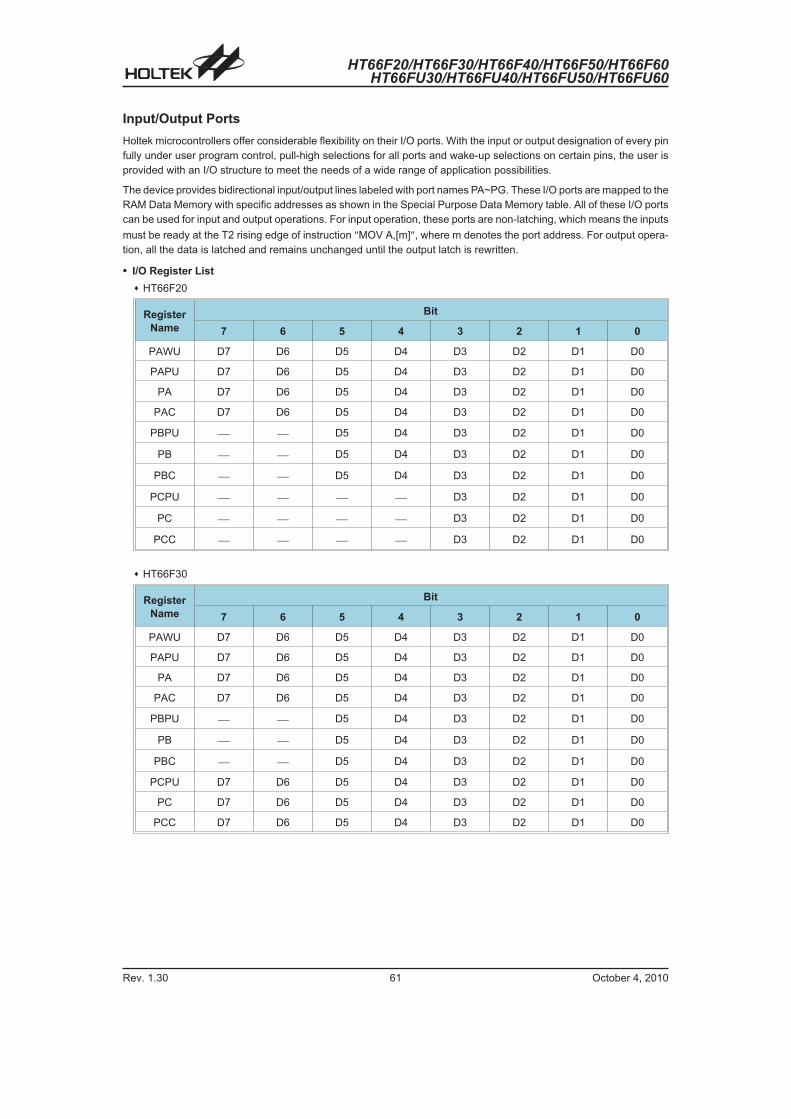
HT66F20/HT66F30/HT66F40/HT66F50/HT66F60HT66FU30/HT66FU40/HT66FU50/HT66FU60
Rev. 1.30 61 October 4, 2010
Input/Output Ports
Holtek microcontrollers offer considerable flexibility on their I/O ports. With the input or output designation of every pin
fully under user program control, pull-high selections for all ports and wake-up selections on certain pins, the user is
provided with an I/O structure to meet the needs of a wide range of application possibilities.
The device provides bidirectional input/output lines labeled with port names PA~PG. These I/O ports are mapped to the
RAM Data Memory with specific addresses as shown in the Special Purpose Data Memory table. All of these I/O ports
can be used for input and output operations. For input operation, these ports are non-latching, which means the inputs
must be ready at the T2 rising edge of instruction �MOV A,[m]�, where m denotes the port address. For output opera-
tion, all the data is latched and remains unchanged until the output latch is rewritten.
� I/O Register List
HT66F20
Register
Name
Bit
7 6 5 4 3 2 1 0
PAWU D7 D6 D5 D4 D3 D2 D1 D0
PAPU D7 D6 D5 D4 D3 D2 D1 D0
PA D7 D6 D5 D4 D3 D2 D1 D0
PAC D7 D6 D5 D4 D3 D2 D1 D0
PBPU � � D5 D4 D3 D2 D1 D0
PB � � D5 D4 D3 D2 D1 D0
PBC � � D5 D4 D3 D2 D1 D0
PCPU � � � � D3 D2 D1 D0
PC � � � � D3 D2 D1 D0
PCC � � � � D3 D2 D1 D0
HT66F30
Register
Name
Bit
7 6 5 4 3 2 1 0
PAWU D7 D6 D5 D4 D3 D2 D1 D0
PAPU D7 D6 D5 D4 D3 D2 D1 D0
PA D7 D6 D5 D4 D3 D2 D1 D0
PAC D7 D6 D5 D4 D3 D2 D1 D0
PBPU � � D5 D4 D3 D2 D1 D0
PB � � D5 D4 D3 D2 D1 D0
PBC � � D5 D4 D3 D2 D1 D0
PCPU D7 D6 D5 D4 D3 D2 D1 D0
PC D7 D6 D5 D4 D3 D2 D1 D0
PCC D7 D6 D5 D4 D3 D2 D1 D0

HT66F20/HT66F30/HT66F40/HT66F50/HT66F60HT66FU30/HT66FU40/HT66FU50/HT66FU60
Rev. 1.30 62 October 4, 2010
HT66F40/HT66F50
Register
Name
Bit
7 6 5 4 3 2 1 0
PAWU D7 D6 D5 D4 D3 D2 D1 D0
PAPU D7 D6 D5 D4 D3 D2 D1 D0
PA D7 D6 D5 D4 D3 D2 D1 D0
PAC D7 D6 D5 D4 D3 D2 D1 D0
PBPU D7 D6 D5 D4 D3 D2 D1 D0
PB D7 D6 D5 D4 D3 D2 D1 D0
PBC D7 D6 D5 D4 D3 D2 D1 D0
PCPU D7 D6 D5 D4 D3 D2 D1 D0
PC D7 D6 D5 D4 D3 D2 D1 D0
PCC D7 D6 D5 D4 D3 D2 D1 D0
PDPU D7 D6 D5 D4 D3 D2 D1 D0
PD D7 D6 D5 D4 D3 D2 D1 D0
PDC D7 D6 D5 D4 D3 D2 D1 D0
PEPU D7 D6 D5 D4 D3 D2 D1 D0
PE D7 D6 D5 D4 D3 D2 D1 D0
PEC D7 D6 D5 D4 D3 D2 D1 D0
PFPU � � � � � � D1 D0
PF � � � � � � D1 D0
PFC � � � � � � D1 D0

HT66F20/HT66F30/HT66F40/HT66F50/HT66F60HT66FU30/HT66FU40/HT66FU50/HT66FU60
Rev. 1.30 63 October 4, 2010
HT66F60
Register
Name
Bit
7 6 5 4 3 2 1 0
PAWU D7 D6 D5 D4 D3 D2 D1 D0
PAPU D7 D6 D5 D4 D3 D2 D1 D0
PA D7 D6 D5 D4 D3 D2 D1 D0
PAC D7 D6 D5 D4 D3 D2 D1 D0
PBPU D7 D6 D5 D4 D3 D2 D1 D0
PB D7 D6 D5 D4 D3 D2 D1 D0
PBC D7 D6 D5 D4 D3 D2 D1 D0
PCPU D7 D6 D5 D4 D3 D2 D1 D0
PC D7 D6 D5 D4 D3 D2 D1 D0
PCC D7 D6 D5 D4 D3 D2 D1 D0
PDPU D7 D6 D5 D4 D3 D2 D1 D0
PD D7 D6 D5 D4 D3 D2 D1 D0
PDC D7 D6 D5 D4 D3 D2 D1 D0
PEPU D7 D6 D5 D4 D3 D2 D1 D0
PE D7 D6 D5 D4 D3 D2 D1 D0
PEC D7 D6 D5 D4 D3 D2 D1 D0
PFPU D7 D6 D5 D4 D3 D2 D1 D0
PF D7 D6 D5 D4 D3 D2 D1 D0
PFC D7 D6 D5 D4 D3 D2 D1 D0
PGPU � � � � � � D1 D0
PG � � � � � � D1 D0
PGC � � � � � � D1 D0

HT66F20/HT66F30/HT66F40/HT66F50/HT66F60HT66FU30/HT66FU40/HT66FU50/HT66FU60
Rev. 1.30 64 October 4, 2010
Pull-high Resistors
Many product applications require pull-high resistors for their switch inputs usually requiring the use of an external re-
sistor. To eliminate the need for these external resistors, all I/O pins, when configured as an input have the capability of
being connected to an internal pull-high resistor. These pull-high resistors are selected using registers PAPU~PGPU,
and are implemented using weak PMOS transistors.
� PAPU Register
Bit 7 6 5 4 3 2 1 0
Name D7 D6 D5 D4 D3 D2 D1 D0
R/W R/W R/W R/W R/W R/W R/W R/W R/W
POR 0 0 0 0 0 0 0 0
� PBPU Register
HT66F40/HT66F50/HT66F60
Bit 7 6 5 4 3 2 1 0
Name D7 D6 D5 D4 D3 D2 D1 D0
R/W R/W R/W R/W R/W R/W R/W R/W R/W
POR 0 0 0 0 0 0 0 0
� PCPU Register
HT66F30/HT66F40/HT66F50/HT66F60
Bit 7 6 5 4 3 2 1 0
Name D7 D6 D5 D4 D3 D2 D1 D0
R/W R/W R/W R/W R/W R/W R/W R/W R/W
POR 0 0 0 0 0 0 0 0
� PDPU Register
HT66F40/HT66F50/HT66F60
Bit 7 6 5 4 3 2 1 0
Name D7 D6 D5 D4 D3 D2 D1 D0
R/W R/W R/W R/W R/W R/W R/W R/W R/W
POR 0 0 0 0 0 0 0 0
� PEPU Register
HT66F40/HT66F50/HT66F60
Bit 7 6 5 4 3 2 1 0
Name D7 D6 D5 D4 D3 D2 D1 D0
R/W R/W R/W R/W R/W R/W R/W R/W R/W
POR 0 0 0 0 0 0 0 0

HT66F20/HT66F30/HT66F40/HT66F50/HT66F60HT66FU30/HT66FU40/HT66FU50/HT66FU60
Rev. 1.30 65 October 4, 2010
� PFPU Register
HT66F60
Bit 7 6 5 4 3 2 1 0
Name D7 D6 D5 D4 D3 D2 D1 D0
R/W R/W R/W R/W R/W R/W R/W R/W R/W
POR 0 0 0 0 0 0 0 0
Bit 7~0 I/O Port bit 7 ~ bit 0 Pull-High Control
0: Disable
1: Enable
� PBPU Register
HT66F20/HT66F30
Bit 7 6 5 4 3 2 1 0
Name � � D5 D4 D3 D2 D1 D0
R/W � � R/W R/W R/W R/W R/W R/W
POR � � 0 0 0 0 0 0
Bit 7~6 ��� Unimplemented, read as �0�
Bit 5~0 PBPU: Port B bit 5 ~ bit 0 Pull-High Control
0: Disable
1: Enable
� PCPU Register
HT66F20
Bit 7 6 5 4 3 2 1 0
Name � � � � D3 D2 D1 D0
R/W � � � � R/W R/W R/W R/W
POR � � � � 0 0 0 0
Bit 7~4 ��� Unimplemented, read as �0�
Bit 3~0 PCPU: Port C bit 3 ~ bit 0 Pull-High Control
0: Disable
1: Enable
� PFPU Register
HT66F40/HT66F50
Bit 7 6 5 4 3 2 1 0
Name � � � � � � D1 D0
R/W � � � � � � R/W R/W
POR � � � � � � 0 0
Bit 7~2 ��� Unimplemented, read as �0�
Bit 1~0 PFPU: Port F bit 1 ~ bit 0 Pull-High Control
0: Disable
1: Enable

HT66F20/HT66F30/HT66F40/HT66F50/HT66F60HT66FU30/HT66FU40/HT66FU50/HT66FU60
Rev. 1.30 66 October 4, 2010
� PGPU Register
HT66F60
Bit 7 6 5 4 3 2 1 0
Name � � � � � � D1 D0
R/W � � � � � � R/W R/W
POR � � � � � � 0 0
Bit 7~2 ��� Unimplemented, read as �0�
Bit 1~0 PGPU: Port G bit 1 ~ bit 0 Pull-High Control
0: Disable
1: Enable
Port A Wake-up
The HALT instruction forces the microcontroller into the SLEEP or IDLE Mode which preserves power, a feature that is
important for battery and other low-power applications. Various methods exist to wake-up the microcontroller, one of
which is to change the logic condition on one of the Port A pins from high to low. This function is especially suitable for
applications that can be woken up via external switches. Each pin on Port A can be selected individually to have this
wake-up feature using the PAWU register.
� PAWU Register
Bit 7 6 5 4 3 2 1 0
Name D7 D6 D5 D4 D3 D2 D1 D0
R/W R/W R/W R/W R/W R/W R/W R/W R/W
POR 0 0 0 0 0 0 0 0
Bit 7~0 PAWU: Port A bit 7 ~ bit 0 Wake-up Control
0: Disable
1: Enable
I/O Port Control Registers
Each I/O port has its own control register known as PAC~PGC, to control the input/output configuration. With this con-
trol register, each CMOS output or input can be reconfigured dynamically under software control. Each pin of the I/O
ports is directly mapped to a bit in its associated port control register. For the I/O pin to function as an input, the corre-
sponding bit of the control register must be written as a �1�. This will then allow the logic state of the input pin to be di-
rectly read by instructions. When the corresponding bit of the control register is written as a �0�, the I/O pin will be setup
as a CMOS output. If the pin is currently setup as an output, instructions can still be used to read the output register.
However, it should be noted that the program will in fact only read the status of the output data latch and not the actual
logic status of the output pin.
� PAC Register
Bit 7 6 5 4 3 2 1 0
Name D7 D6 D5 D4 D3 D2 D1 D0
R/W R/W R/W R/W R/W R/W R/W R/W R/W
POR 1 1 1 1 1 1 1 1
� PBC Register
HT66F40/HT66F50/HT66F60
Bit 7 6 5 4 3 2 1 0
Name D7 D6 D5 D4 D3 D2 D1 D0
R/W R/W R/W R/W R/W R/W R/W R/W R/W
POR 1 1 1 1 1 1 1 1

HT66F20/HT66F30/HT66F40/HT66F50/HT66F60HT66FU30/HT66FU40/HT66FU50/HT66FU60
Rev. 1.30 67 October 4, 2010
� PCC Register
HT66F30/HT66F40/HT66F50/HT66F60
Bit 7 6 5 4 3 2 1 0
Name D7 D6 D5 D4 D3 D2 D1 D0
R/W R/W R/W R/W R/W R/W R/W R/W R/W
POR 1 1 1 1 1 1 1 1
� PDC Register
HT66F40/HT66F50/HT66F60
Bit 7 6 5 4 3 2 1 0
Name D7 D6 D5 D4 D3 D2 D1 D0
R/W R/W R/W R/W R/W R/W R/W R/W R/W
POR 1 1 1 1 1 1 1 1
� PEC Register
HT66F40/HT66F50/HT66F60
Bit 7 6 5 4 3 2 1 0
Name D7 D6 D5 D4 D3 D2 D1 D0
R/W R/W R/W R/W R/W R/W R/W R/W R/W
POR 1 1 1 1 1 1 1 1
� PFC Register
HT66F60
Bit 7 6 5 4 3 2 1 0
Name D7 D6 D5 D4 D3 D2 D1 D0
R/W R/W R/W R/W R/W R/W R/W R/W R/W
POR 1 1 1 1 1 1 1 1
Bit 7~0 I/O Port bit 7 ~ bit 0 Input/Output Control
0: Output
1: Input
� PBC Register
HT66F20/HT66F30
Bit 7 6 5 4 3 2 1 0
Name � � D5 D4 D3 D2 D1 D0
R/W � � R/W R/W R/W R/W R/W R/W
POR � � 0 0 0 0 0 0
Bit 7~6 ��� Unimplemented, read as �0�
Bit 5~0 PBC: Port B bit 5 ~ bit 0 Input/Output Control
0: Output
1: Input

HT66F20/HT66F30/HT66F40/HT66F50/HT66F60HT66FU30/HT66FU40/HT66FU50/HT66FU60
Rev. 1.30 68 October 4, 2010
� PCC Register
HT66F20
Bit 7 6 5 4 3 2 1 0
Name � � � � D3 D2 D1 D0
R/W � � � � R/W R/W R/W R/W
POR � � � � 0 0 0 0
Bit 7~4 ��� Unimplemented, read as �0�
Bit 3~0 PCC: Port C bit 3 ~ bit 0 Input/Output Control
0: Output
1: Input
� PFC Register
HT66F40/HT66F50
Bit 7 6 5 4 3 2 1 0
Name � � � � � � D1 D0
R/W � � � � � � R/W R/W
POR � � � � � � 0 0
Bit 7~2 ��� Unimplemented, read as �0�
Bit 1~0 PFC: Port F bit 1 ~ bit 0 Input/Output Control
0: Output
1: Input
� PGC Register
HT66F60
Bit 7 6 5 4 3 2 1 0
Name � � � � � � D1 D0
R/W � � � � � � R/W R/W
POR � � � � � � 0 0
Bit 7~2 ��� Unimplemented, read as �0�
Bit 1~0 PGC: Port G bit 1 ~ bit 0 Input/Output Control
0: Output
1: Input

HT66F20/HT66F30/HT66F40/HT66F50/HT66F60HT66FU30/HT66FU40/HT66FU50/HT66FU60
Rev. 1.30 69 October 4, 2010
Pin-remapping Functions
The flexibility of the microcontroller range is greatly enhanced by the use of pins that have more than one function.
Limited numbers of pins can force serious design constraints on designers but by supplying pins with multi-functions,
many of these difficulties can be overcome. The way in which the pin function of each pin is selected is different for each
function and a priority order is established where more than one pin function is selected simultaneously. Additionally
there are a series of PRM0, PRM1 and PRM2 registers to establish certain pin functions.
Pin-remapping Registers
The limited number of supplied pins in a package can impose restrictions on the amount of functions a certain device
can contain. However by allowing the same pins to share several different functions and providing a means of function
selection, a wide range of different functions can be incorporated into even relatively small package sizes. Some de-
vices include PRM0, PRM1 or PRM2 registers which can select the functions of certain pins.
� Pin-remapping Register List
HT66F30
Register
Name
Bit
7 6 5 4 3 2 1 0
PRM0 � � � � � PCPRM SIMPS0 PCKPS
HT66F40
Register
Name
Bit
7 6 5 4 3 2 1 0
PRM0 � C1XPS0 � C0XPS0 PDPRM SIMPS1 SIMPS0 PCKPS
PRM1 TCK2PS TCK1PS TCK0PS � INT1PS1 INT1PS0 INT0PS1 INT0PS0
PRM2 � � TP21PS TP20PS TP1B2PS TP1APS TP01PS TP00PS
HT66F50
Register
Name
Bit
7 6 5 4 3 2 1 0
PRM0 � C1XPS0 � C0XPS0 PDPRM SIMPS1 SIMPS0 PCKPS
PRM1 TCK2PS TCK1PS TCK0PS � INT1PS1 INT1PS0 INT0PS1 INT0PS0
PRM2 TP31PS TP30PS TP21PS TP20PS TP1B2PS TP1APS TP01PS TP00PS
HT66F60
Register
Name
Bit
7 6 5 4 3 2 1 0
PRM0 C1XPS1 C1XPS0 C0XPS1 C0XPS0 PDPRM SIMPS1 SIMPS0 PCKPS
PRM1 TCK2PS TCK1PS TCK0PS INT2PS1 INT1PS1 INT1PS0 INT0PS1 INT0PS0
PRM2 TP31PS TP30PS TP21PS TP20PS TP1B2PS TP1APS TP01PS TP00PS

HT66F20/HT66F30/HT66F40/HT66F50/HT66F60HT66FU30/HT66FU40/HT66FU50/HT66FU60
Rev. 1.30 70 October 4, 2010
� PRM0 Register
HT66F30
Bit 7 6 5 4 3 2 1 0
Name � � � � � PCPRM SIMPS0 PCKPS
R/W � � � � � R/W R/W R/W
POR � � � � � 0 0 0
Bit 7~3 ��� Unimplemented, read as �0�
Bit 2 PCPRM: PC1~PC0 pin-shared function Pin Remapping Control
0: No change
1: TP1B_0 on PC0 change to PA6, TP1B_1 on PC1 change to PA7 if SIMPS0=1
Bit 1 SIMPS0: SIM Pin Remapping Control
0: SDO on PA5; SDI/SDA on PA6; SCK/SCL on PA7; SCS on PB5
1: SDO on PC1; SDI/SDA on PC0; SCK/SCL on PC7; SCS on PC6
Bit 0 PCKPS: PCK and PINT Pin Remapping Control
0: PCK on PC2; PINT on PC3
1: PCK on PC5; PINT on PC4
� PRM0 Register
HT66F40/HT66F50
Bit 7 6 5 4 3 2 1 0
Name � C1XPS0 � C0XPS0 PDPRM SIMPS1 SIMPS0 PCKPS
R/W � R/W � R/W R/W R/W R/W R/W
POR � 0 � 0 0 0 0 0
Bit 7 ��� Unimplemented, read as �0�
Bit 6 C1XPS0: C1X Pin Remapping Control
0: C1X on PA5
1: C1X on PF1
Bit 5 ��� Unimplemented, read as �0�
Bit 4 C0XPS0: C0X Pin Remapping Control
0: C0X on PA0
1: C0X on PF0
Bit 3 PDPRM: PD3~PD0 pin-shared function Pin Remapping Control
0: No change
1: TCK2 on PD0 change to PB6, TP2_0 on PD1 change to PB7, TCK0 on PD2 change to PD6,
TCK1 on PD3 change to PD7 if SIMPS1, SIMPS0=01
Bit 2~1 SIMPS1, SIMPS0: SIM Pin Remapping Control
00: SDO on PA5; SDI/SDA on PA6; SCK/SCL on PA7; SCS on PB5
01: SDO on PD3; SDI/SDA on PD2; SCK/SCL on PD1; SCS on PD0
10: SDO on PB6; SDI/SDA on PB7; SCK/SCL on PD6; SCS on PD7
11: Undefined
Bit 0 PCKPS: PCK and PINT Pin Remapping Control
0: PCK on PC2; PINT on PC3
1: PCK on PC5; PINT on PC4

HT66F20/HT66F30/HT66F40/HT66F50/HT66F60HT66FU30/HT66FU40/HT66FU50/HT66FU60
Rev. 1.30 71 October 4, 2010
� PRM0 Register
HT66F60
Bit 7 6 5 4 3 2 1 0
Name C1XPS1 C1XPS0 C0XPS1 C0XPS0 PDPRM SIMPS1 SIMPS0 PCKPS
R/W R/W R/W R/W R/W R/W R/W R/W R/W
POR 0 0 0 0 0 0 0 0
Bit 7~6 C1XPS1, C1XPS0: C1X Pin Remapping Control
00: C1X on PA5
01: C1X on PF1
10: C1X on PG1
11: Undefined
Bit 5~4 C0XPS1, C0XPS0: C0X Pin Remapping Control
00: C0X on PA0
01: C0X on PF0
10: C0X on PG0
11: Undefined
Bit 3 PDPRM: PD3~PD0 pin-shared function Pin Remapping Control
0: No change
1: TCK2 on PD0 change to PB6, TP2_0 on PD1 change to PB7, TCK0 on PD2 change to PD6,
TCK1 on PD3 change to PD7 if SIMPS1, SIMPS0=01 or 11
Bit 2~1 SIMPS1, SIMPS0: SIM Pin Remapping Control
00: SDO on PA5; SDI/SDA on PA6; SCK/SCL on PA7; SCS on PB5
01: SDO on PD3; SDI/SDA on PD2; SCK/SCL on PD1; SCS on PD0
10: SDO on PB6; SDI/SDA on PB7; SCK/SCL on PD6; SCS on PD7
11: SDO on PD1; SDI/SDA on PD2; SCK/SCL on PD3; SCS on PD0
Bit 0 PCKPS: PCK and PINT Pin Remapping Control
0: PCK on PC2; PINT on PC3
1: PCK on PC5; PINT on PC4
� PRM1 Register
HT66F40/HT66F50
Bit 7 6 5 4 3 2 1 0
Name TCK2PS TCK1PS TCK0PS � INT1PS1 INT1PS0 INT0PS1 INT0PS0
R/W R/W R/W R/W � R/W R/W R/W R/W
POR 0 0 0 � 0 0 0 0
Bit 7 TCK2PS: TCK2 Pin Remapping Control
0: TCK2 on PC2
1: TCK2 on PD0
Bit 6 TCK1PS: TCK1 Pin Remapping Control
0: TCK1 on PA4
1: TCK1 on PD3
Bit 5 TCK0PS: TCK0 Pin Remapping Control
0: TCK0 on PA2
1: TCK0 on PD2
Bit 4 ��� Unimplemented, read as �0�
Bit 3~2 INT1PS1, INT1PS0: INT1 Pin Remapping Control
00: INT1 on PA4
01: INT1 on PC5
10: Undefined
11: INT1 on PE7
Bit 1~0 INT0PS1, INT0PS0: INT0 Pin Remapping Control
00: INT0 on PA3
01: INT0 on PC4
10: Undefined
11: INT0 on PE6

HT66F20/HT66F30/HT66F40/HT66F50/HT66F60HT66FU30/HT66FU40/HT66FU50/HT66FU60
Rev. 1.30 72 October 4, 2010
� PRM1 Register
HT66F60
Bit 7 6 5 4 3 2 1 0
Name TCK2PS TCK1PS TCK0PS INT2PS INT1PS1 INT1PS0 INT0PS1 INT0PS0
R/W R/W R/W R/W R/W R/W R/W R/W R/W
POR 0 0 0 0 0 0 0 0
Bit 7 TCK2PS: TCK2 Pin Remapping Control
0: TCK2 on PC2
1: TCK2 on PD0
Bit 6 TCK1PS: TCK1 Pin Remapping Control
0: TCK1 on PA4
1: TCK1 on PD3
Bit 5 TCK0PS: TCK0 Pin Remapping Control
0: TCK0 on PA2
1: TCK0 on PD2
Bit 4 INT2PS: INT2 Pin Remapping Control
0: INT2 on PC4
1: INT2 on PE2
Bit 3~2 INT1PS1, INT1PS0: INT1 Pin Remapping Control
00: INT1 on PA4
01: INT1 on PC5
10: INT1 on PE1
11: INT1 on PE7
Bit 1~0 INT0PS1, INT0PS0: INT0 Pin Remapping Control
00: INT0 on PA3
01: INT0 on PC4
10: INT0 on PE0
11: INT0 on PE6
� PRM2 Register
HT66F40
Bit 7 6 5 4 3 2 1 0
Name � � TP21PS TP20PS TP1B2PS TP1APS TP01PS TP00PS
R/W � � R/W R/W R/W R/W R/W R/W
POR � � 0 0 0 0 0 0
Bit 7~6 ��� Unimplemented, read as �0�
Bit 5 TP21PS: TP2_1 Pin Remapping Control
0: TP2_1 on PC4
1: TP2_1 on PD4
Bit 4 TP20PS: TP2_0 Pin Remapping Control
0: TP2_0 on PC3
1: TP2_0 on PD1
Bit 3 TP1B2PS: TP1B_2 Pin Remapping Control
0: TP1B_2 on PC5
1: TP1B_2 on PE4
Bit 2 TP1APS: TP1A Pin Remapping Control
0: TP1A on PA1
1: TP1A on PC7
Bit 1 TP01PS: TP0_1 Pin Remapping Control
0: TP0_1 on PC5
1: TP0_1 on PD5
Bit 0 TP00PS: TP0_0 Pin Remapping Control
0: TP0_0 on PA0
1: TP0_0 on PC6

HT66F20/HT66F30/HT66F40/HT66F50/HT66F60HT66FU30/HT66FU40/HT66FU50/HT66FU60
Rev. 1.30 73 October 4, 2010
� PRM2 Register
HT66F50/HT66F60
Bit 7 6 5 4 3 2 1 0
Name TP31PS TP30PS TP21PS TP20PS TP1B2PS TP1APS TP01PS TP00PS
R/W R/W R/W R/W R/W R/W R/W R/W R/W
POR 0 0 0 0 0 0 0 0
Bit 7 TP31PS: TP3_1 Pin Remapping Control
0: TP3_1 on PD0
1: TP3_1 on PE3
Bit 6 TP30PS: TP3_0 Pin Remapping Control
0: TP3_0 on PD3
1: TP3_0 on PE5
Bit 5 TP21PS: TP2_1 Pin Remapping Control
0: TP2_1 on PC4
1: TP2_1 on PD4
Bit 4 TP20PS: TP2_0 Pin Remapping Control
0: TP2_0 on PC3
1: TP2_0 on PD1
Bit 3 TP1B2PS: TP1B_2 Pin Remapping Control
0: TP1B_2 on PC5
1: TP1B_2 on PE4
Bit 2 TP1APS: TP1A Pin Remapping Control
0: TP1A on PA1
1: TP1A on PC7
Bit 1 TP01PS: TP0_1 Pin Remapping Control
0: TP0_1 on PC5
1: TP0_1 on PD5
Bit 0 TP00PS: TP0_0 Pin Remapping Control
0: TP0_0 on PA0
1: TP0_0 on PC6

HT66F20/HT66F30/HT66F40/HT66F50/HT66F60HT66FU30/HT66FU40/HT66FU50/HT66FU60
Rev. 1.30 74 October 4, 2010
I/O Pin Structures
The accompanying diagrams illustrate the internal
structures of some generic I/O pin types. As the exact
logical construction of the I/O pin will differ from these
drawings, they are supplied as a guide only to assist
with the functional understanding of the I/O pins. The
wide range of pin-shared structures does not permit all
types to be shown.
Programming Considerations
Within the user program, one of the first things to con-
sider is port initialisation. After a reset, all of the I/O data
and port control registers will be set high. This means
that all I/O pins will default to an input state, the level of
which depends on the other connected circuitry and
whether pull-high selections have been chosen. If the
port control registers, PAC~PGC, are then programmed
to setup some pins as outputs, these output pins will
have an initial high output value unless the associated
port data registers, PA~PG, are first programmed. Se-
lecting which pins are inputs and which are outputs can
be achieved byte-wide by loading the correct values into
the appropriate port control register or by programming
individual bits in the port control register using the �SET
[m].i� and �CLR [m].i� instructions. Note that when using
these bit control instructions, a read-modify-write opera-
tion takes place. The microcontroller must first read in
the data on the entire port, modify it to the required new
bit values and then rewrite this data back to the output
ports.
Port A has the additional capability of providing wake-up
functions. When the device is in the SLEEP or IDLE
Mode, various methods are available to wake the device
up. One of these is a high to low transition of any of the
Port A pins. Single or multiple pins on Port A can be
setup to have this function.
� � �
>72
; � / � @ � � � � � � � �� ! � � � � ; � / � @ �
� � # � � � � � � � & � � � � �
� G
� ?
�
� G
� ?
�
� � � � � � � � : � �
� � � � � : � �
; � � � � � � � � � � � � � � & � � � � �
� % � � � � � �
� � # � � � � � � � � � � & � � � � �
; � � � � � � � � � � � & � � � � �
� � � � � : � �
+ ( � � � �
G
G
6 $ � � � � !
; � � /6 � � � @ �
6 � � � @ 0 � & % � & � � � � �� � � � � �
Generic Input/Output Structure

HT66F20/HT66F30/HT66F40/HT66F50/HT66F60HT66FU30/HT66FU40/HT66FU50/HT66FU60
Rev. 1.30 75 October 4, 2010
� � �
>72
� � # � � � � � � � & � � � � �
� � � � � � � � : � �
� � � � � : � �
; � � � � � � � � � � � � � � & � � � � �
� % � � � � � �
� � # � � � � � � � � � � & � � � � �
; � � � � � � � � � � � & � � � � �
� � � � � : � �
$ ( � � + � � � � 6 � � �
$ � � , = $ � � �
� � � $ ( � � � � � ) � � � � �
; � � /6 � � � @ �
$ � � � � &+ � � �
� � � � � � � �
� G
� ?�
G
� G
� ?�
G
6 � � � @ 0 � & % � & � � � � �� � � � � �
A/D Input/Output Structure

HT66F20/HT66F30/HT66F40/HT66F50/HT66F60HT66FU30/HT66FU40/HT66FU50/HT66FU60
Rev. 1.30 76 October 4, 2010
Timer Modules � TM
One of the most fundamental functions in any
microcontroller device is the ability to control and mea-
sure time. To implement time related functions each de-
vice includes several Timer Modules, abbreviated to the
name TM. The TMs are multi-purpose timing units and
serve to provide operations such as Timer/Counter, In-
put Capture, Compare Match Output and Single Pulse
Output as well as being the functional unit for the gener-
ation of PWM signals. Each of the TMs has either two or
three individual interrupts. The addition of input and out-
put pins for each TM ensures that users are provided
with timing units with a wide and flexible range of fea-
tures.
The common features of the different TM types are de-
scribed here with more detailed information provided in
the individual Compact, Standard and Enhanced TM
sections.
Introduction
The devices contain from two to four TMs depending
upon which device is selected with each TM having a
reference name of TM0, TM1, TM2 and TM3. Each indi-
vidual TM can be categorised as a certain type, namely
Compact Type TM, Standard Type TM or Enhanced
Type TM. Although similar in nature, the different TM
types vary in their feature complexity. The common fea-
tures to all of the Compact, Standard and Enhanced
TMs will be described in this section, the detailed opera-
tion regarding each of the TM types will be described in
separate sections. The main features and differences
between the three types of TMs are summarised in the
accompanying table.
Function CTM STM ETM
Timer/Counter � � �
I/P Capture � � �
Compare Match Output � � �
PWM Channels 1 1 2
Single Pulse Output � 1 2
PWM Alignment Edge Edge Edge & Centre
PWM Adjustment Period & Duty Duty or Period Duty or Period Duty or Period
TM Function Summary
Each device in the series contains a specific number of either Compact Type, Standard Type and Enhanced Type TM
units which are shown in the table together with their individual reference name, TM0~TM3.
Device TM0 TM1 TM2 TM3
HT66F20 10-bit CTM 10-bit STM � �
HT66F30 10-bit CTM 10-bit ETM � �
HT66F40 10-bit CTM 10-bit ETM 16-bit STM �
HT66F50 10-bit CTM 10-bit ETM 16-bit STM 10-bit CTM
HT66F60 10-bit CTM 10-bit ETM 16-bit STM 10-bit CTM
TM Name/Type Reference

HT66F20/HT66F30/HT66F40/HT66F50/HT66F60HT66FU30/HT66FU40/HT66FU50/HT66FU60
Rev. 1.30 77 October 4, 2010
TM Operation
The three different types of TM offer a diverse range of
functions, from simple timing operations to PWM signal
generation. The key to understanding how the TM oper-
ates is to see it in terms of a free running counter whose
value is then compared with the value of
pre-programmed internal comparators. When the free
running counter has the same value as the
pre-programmed comparator, known as a compare
match situation, a TM interrupt signal will be generated
which can clear the counter and perhaps also change
the condition of the TM output pin. The internal TM
counter is driven by a user selectable clock source,
which can be an internal clock or an external pin.
TM Clock Source
The clock source which drives the main counter in each
TM can originate from various sources. The selection of
the required clock source is implemented using the
TnCK2~TnCK0 bits in the TM control registers. The
clock source can be a ratio of either the system clock
fSYS or the internal high clock fH, the fTBC clock source or
the external TCKn pin. Note that setting these bits to the
value 101 will select a reserved clock input, in effect dis-
connecting the TM clock source. The TCKn pin clock
source is used to allow an external signal to drive the TM
as an external clock source or for event counting.
TM Interrupts
The Compact and Standard type TMs each have two in-
ternal interrupts, one for each of the internal comparator
A or comparator P, which generate a TM interrupt when
a compare match condition occurs. As the Enhanced
type TM has three internal comparators and comparator
A or comparator B or comparator P compare match
functions, it consequently has three internal interrupts.
When a TM interrupt is generated it can be used to clear
the counter and also to change the state of the TM out-
put pin.
TM External Pins
Each of the TMs, irrespective of what type, has one TM
input pin, with the label TCKn. The TM input pin, is es-
sentially a clock source for the TM and is selected using
the TnCK2~TnCK0 bits in the TMnC0 register. This ex-
ternal TM input pin allows an external clock source to
drive the internal TM. This external TM input pin is
shared with other functions but will be connected to the
internal TM if selected using the TnCK2~TnCK0 bits.
The TM input pin can be chosen to have either a rising or
falling active edge.
The TMs each have one or more output pins with the la-
bel TPn. When the TM is in the Compare Match Output
Mode, these pins can be controlled by the TM to switch
to a high or low level or to toggle when a compare match
situation occurs. The external TPn output pin is also the
pin where the TM generates the PWM output waveform.
As the TM output pins are pin-shared with other func-
tion, the TM output function must first be setup using
registers. A single bit in one of the registers determines if
its associated pin is to be used as an external TM output
pin or if it is to have another function. The number of out-
put pins for each TM type and device is different, the de-
tails are provided in the accompanying table.
All TM output pin names have an �_n� suffix. Pin names
that include a �_1� or �_2� suffix indicate that they are
from a TM with multiple output pins. This allows the TM
to generate a complimentary output pair, selected using
the I/O register data bits.
Device CTM STM ETM Registers
HT66F20 TP0_0 TP1_0, TP1_1 � TMPC0
HT66F30 TP0_0, TP0_1 �TP1A, TP1B_0,
TP1B_1TMPC0
HT66F40 TP0_0, TP0_1 TP2_0, TP2_1TP1A, TP1B_0,
TP1B_1, TP1B_2TMPC0, TMPC1
HT66F50TP0_0, TP0_1
TP3_0, TP3_1TP2_0, TP2_1
TP1A, TP1B_0,
TP1B_1, TP1B_2TMPC0, TMPC1
HT66F60TP0_0, TP0_1
TP3_0, TP3_1TP2_0, TP2_1
TP1A, TP1B_0,
TP1B_1, TP1B_2TMPC0, TMPC1
TM Output Pins

HT66F20/HT66F30/HT66F40/HT66F50/HT66F60HT66FU30/HT66FU40/HT66FU50/HT66FU60
Rev. 1.30 78 October 4, 2010
TM Input/Output Pin Control Registers
Selecting to have a TM input/output or whether to retain its other shared function, is implemented using one or two reg-
isters, with a single bit in each register corresponding to a TM input/output pin. Setting the bit high will setup the corre-
sponding pin as a TM input/output, if reset to zero the pin will retain its original other function.
Registers DeviceBit
7 6 5 4 3 2 1 0
TMPC0 HT66F20 � � T1CP1 T1CP0 � � � T0CP0
TMPC0 HT66F30 T1ACP0 � T1BCP1 T1BCP0 � � T0CP1 T0CP0
TMPC0
HT66F40
HT66F50
HT66F60
T1ACP0 T1BCP2 T1BCP1 T1BCP0 � � T0CP1 T0CP0
TMPC1 HT66F40 � � � � � � T2CP1 T2CP0
TMPC1HT66F50
HT66F60� � T3CP1 T3CP0 � � T2CP1 T2CP0
TM Input/Output Pin Control Registers List
� � � � � � � � �� � � � � � � � � � � � � �
� � � � �
�
�
� � � � � � � �
� � �
� � � � � � � �
� � �
� � � � �
� � � � � � � � � � � � � � �
�
� � �
�
� � � �
� � � � � � � � � � �
� � � � � � � �� � � � � � � �
�
�
� � �
� � � �
� � � � � � � � �
� � � � �
� � � � �
� � � � � � � � � � � � � � �
�
� � �
�
�
�
�
� � � � � � � � � �
� � � � �
� � � � �
HT66F20 TM Function Pin Control Block Diagram
Note: 1. The I/O register data bits shown are used for TM output inversion control.
2. In the Capture Input Mode, the TM pin control register must never enable more than one TM input.

HT66F20/HT66F30/HT66F40/HT66F50/HT66F60HT66FU30/HT66FU40/HT66FU50/HT66FU60
Rev. 1.30 79 October 4, 2010
� � � � � � � �
� � �
� � � � �
� � � � � � � �
� � � � � � � � � � � � � � �
�
� � �
�
� � � �
� � � � � � � � �
� � � � �
� � � � � � � �� � � � � � � � � � � � � �
� � � � � �
�
�
� � � � � � � �
� � � � � � � � � � � � � � � � �
�
� � � � � �
� � � � � � � � � � � � � � �
�
� � �
�
�
� � � � � � � � �
� � � � �
� � � � � � � � � � � � � � �
�
� � �
�
�� � � � � � � �
� � � � � � � � � � � � � � � �
� � � � � � � �� � � � � � � �
�
�
� � �
� � � �� � � � � � � � � �
� � � � � �
� � � � � �
� � � � � � � � � � � � � � �
�
� � �
�
�
�
�
� � � � � � � � � � �
� � � � � �
� � � � � �
HT66F30 TM Function Pin Control Block Diagram
Note: 1. The I/O register data bits shown are used for TM output inversion control.
2. In the Capture Input Mode, the TM pin control register must never enable more than one TM input.

HT66F20/HT66F30/HT66F40/HT66F50/HT66F60HT66FU30/HT66FU40/HT66FU50/HT66FU60
Rev. 1.30 80 October 4, 2010
� � � � � � � �
� � �
� � � � �
� � � � � � � �
� � � � � � � � � � � � � � �
�
� � �
�
� � � �
� � � � � � � � �
� � � � �
� � � � � � � � � � � � � � �
�
� � �
�
�
� � � � � � � � �
� � � � �
� � � � � � � � � � � � � � �
�
� � �
�
� � � �
� � � � � � � � � � �
� � � � � � � �� � � � � � � �
�
�
� � �
� � � �
� � � � � � � � �
� � � � �
� � � � �
� � � � � � � � � � � � � � �
�
� � �
�
�
�
�
� � � � � � � � � �
� � � � �
� � � � �
HT66F40 TM0 & TM2 Function Pin Control Block Diagram
Note: 1. The I/O register data bits shown are used for TM output inversion control.
2. In the Capture Input Mode, the TM pin control register must never enable more than one TM input.

HT66F20/HT66F30/HT66F40/HT66F50/HT66F60HT66FU30/HT66FU40/HT66FU50/HT66FU60
Rev. 1.30 81 October 4, 2010
� � � � � � � �� � � � � � � � � � � � � �
� � � � � �
�
�
� � � � � � � �
� � � � � � � � � � � � � � � � �
�
� � � � � �
� � � � � � � � � � � � � � �
�
� � �
�
�� � � � � � � �
� � � � � � � � � � � � � � � �
� � � � � � � �� � � � � � � �
�
�
� � �
� � � �
� � � � � � � � � �
� � � � � �
� � � � � �
� � � � � � � � � � � � � � �
�
� � �
�
�
�
�
� � � � � � � � � � �
� � � � � �
� � � � � �
� � � � � � � � � � � � � � �
�
� � �
�
�
� � � � � � � � � � �
� � � � � �
�
�
� � � � � �
HT66F40 TM1 Function Pin Control Block Diagram
Note: 1. The I/O register data bits shown are used for TM output inversion control.
2. In the Capture Input Mode, the TM pin control register must never enable more than one TM input.

HT66F20/HT66F30/HT66F40/HT66F50/HT66F60HT66FU30/HT66FU40/HT66FU50/HT66FU60
Rev. 1.30 82 October 4, 2010
� � � � � � � �
� � �
� � � � �
� � � � � � � �
� � � � � � � � � � � � � � �
�
� � �
�
� � � �
� � � � � � � � �
� � � � �
� � � � � � � � � � � � � � �
�
� � �
�
�
� � � � � � � � �
� � � � �
� � � � � � � � � � � � � � �
�
� � �
�
� � � �
� � � � � � � � � � �
� � � � � � � �� � � � � � � �
�
�
� � �
� � � �
� � � � � � � � �
� � � � �
� � � � �
� � � � � � � � � � � � � � �
�
� � �
�
�
�
�
� � � � � � � � � �
� � � � �
� � � � �
� � � � � � � �
� � �
� � � � �
� � � � � � � �
� � � � � � � � � � � � � � �
�
� � �
�
� � � �
� � � � � � � � �
� � � � �
� � � � � � � � � � � � � � �
�
� � �
�
�
� � � � � � � � �
� � � � �
HT66F50 and HT66F60 TM0, TM2, TM3 Function Pin Control Block Diagram
Note: 1. The I/O register data bits shown are used for TM output inversion control.
2. In the Capture Input Mode, the TM pin control register must never enable more than one TM input.
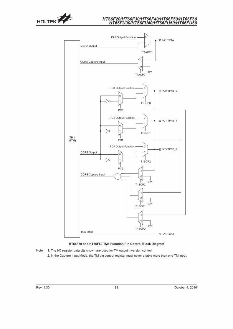
HT66F20/HT66F30/HT66F40/HT66F50/HT66F60HT66FU30/HT66FU40/HT66FU50/HT66FU60
Rev. 1.30 83 October 4, 2010
� � � � � � � �� � � � � � � � � � � � � �
� � � � � �
�
�
� � � � � � � �
� � � � � � � � � � � � � � � � �
�
� � � � � �
� � � � � � � � � � � � � � �
�
� � �
�
�� � � � � � � �
� � � � � � � � � � � � � � � �
� � � � � � � �� � � � � � � �
�
�
� � �
� � � �
� � � � � � � � � �
� � � � � �
� � � � � �
� � � � � � � � � � � � � � �
�
� � �
�
�
�
�
� � � � � � � � � � �
� � � � � �
� � � � � �
� � � � � � � � � � � � � � �
�
� � �
�
�
� � � � � � � � � � �
� � � � � �
�
�
� � � � � �
HT66F50 and HT66F60 TM1 Function Pin Control Block Diagram
Note: 1. The I/O register data bits shown are used for TM output inversion control.
2. In the Capture Input Mode, the TM pin control register must never enable more than one TM input.

HT66F20/HT66F30/HT66F40/HT66F50/HT66F60HT66FU30/HT66FU40/HT66FU50/HT66FU60
Rev. 1.30 84 October 4, 2010
� TMPC0 Register
� HT66F20
Bit 7 6 5 4 3 2 1 0
Name � � T1CP1 T1CP0 � � � T0CP0
R/W � � R/W R/W � � � R/W
POR � � 0 1 � � � 1
Bit 7, 6 Unimplemented, read as �0�
Bit 5 T1CP1: TP1_1 pin Control
0: disable
1: enable
Bit 4 T1CP0: TP1_0 pin Control
0: disable
1: enable
Bit 3~1 Unimplemented, read as �0�
Bit 0 T0CP0: TP0_0 pin Control
0: disable
1: enable
� HT66F30
Bit 7 6 5 4 3 2 1 0
Name T1ACP0 � T1BCP1 T1BCP0 � � T0CP1 T0CP0
R/W R/W � R/W R/W � � R/W R/W
POR 1 � 0 1 � � 0 1
Bit 7 T1ACP0: TP1A pin Control
0: disable
1: enable
Bit 6 Unimplemented, read as �0�
Bit 5 T1BCP1: TP1B_1 pin Control
0: disable
1: enable
Bit 4 T1BCP0: TP1B_0 pin Control
0: disable
1: enable
Bit 3~2 Unimplemented, read as �0�
Bit 1 T0CP1: TP0_1 pin Control
0: disable
1: enable
Bit 0 T0CP0: TP0_0 pin Control
0: disable
1: enable
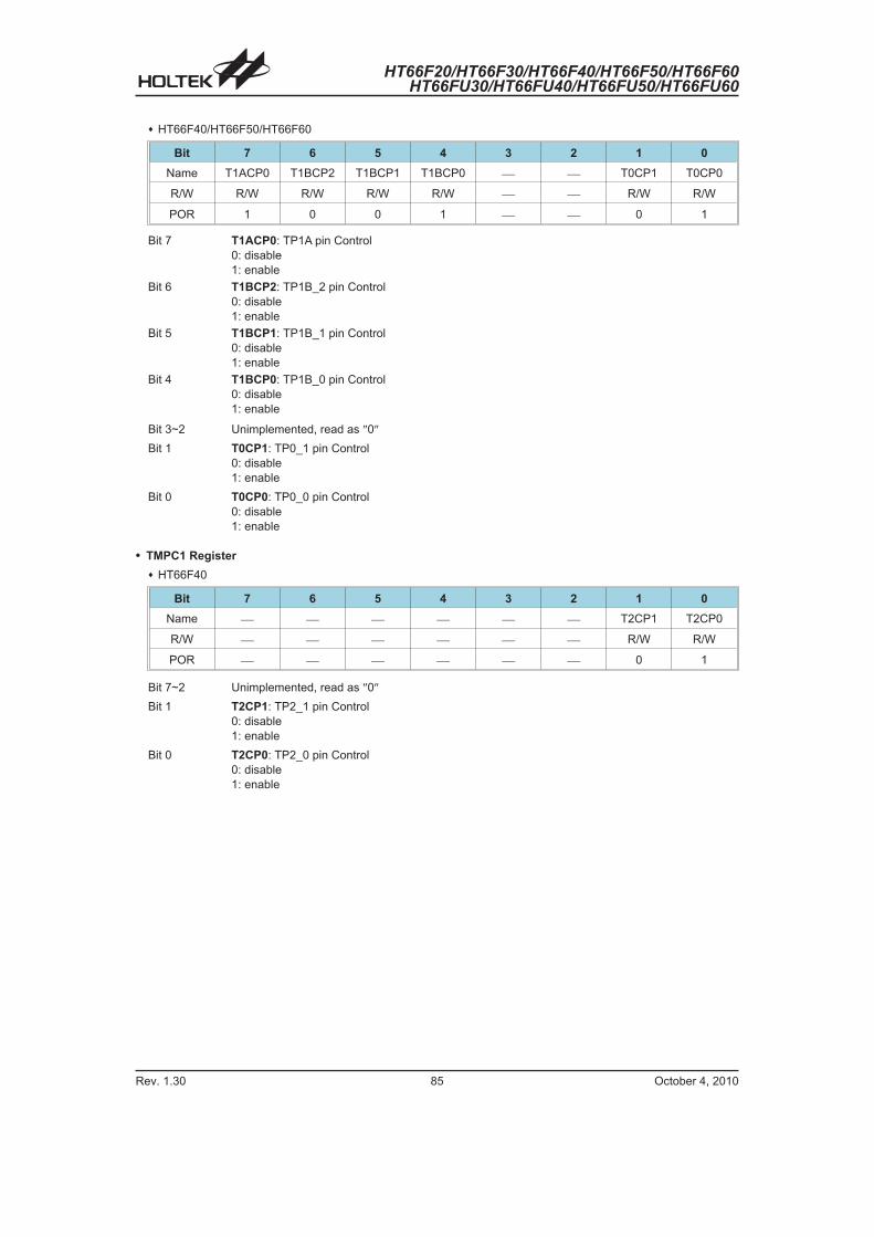
HT66F20/HT66F30/HT66F40/HT66F50/HT66F60HT66FU30/HT66FU40/HT66FU50/HT66FU60
Rev. 1.30 85 October 4, 2010
� HT66F40/HT66F50/HT66F60
Bit 7 6 5 4 3 2 1 0
Name T1ACP0 T1BCP2 T1BCP1 T1BCP0 � � T0CP1 T0CP0
R/W R/W R/W R/W R/W � � R/W R/W
POR 1 0 0 1 � � 0 1
Bit 7 T1ACP0: TP1A pin Control
0: disable
1: enable
Bit 6 T1BCP2: TP1B_2 pin Control
0: disable
1: enable
Bit 5 T1BCP1: TP1B_1 pin Control
0: disable
1: enable
Bit 4 T1BCP0: TP1B_0 pin Control
0: disable
1: enable
Bit 3~2 Unimplemented, read as �0�
Bit 1 T0CP1: TP0_1 pin Control
0: disable
1: enable
Bit 0 T0CP0: TP0_0 pin Control
0: disable
1: enable
� TMPC1 Register
� HT66F40
Bit 7 6 5 4 3 2 1 0
Name � � � � � � T2CP1 T2CP0
R/W � � � � � � R/W R/W
POR � � � � � � 0 1
Bit 7~2 Unimplemented, read as �0�
Bit 1 T2CP1: TP2_1 pin Control
0: disable
1: enable
Bit 0 T2CP0: TP2_0 pin Control
0: disable
1: enable

HT66F20/HT66F30/HT66F40/HT66F50/HT66F60HT66FU30/HT66FU40/HT66FU50/HT66FU60
Rev. 1.30 86 October 4, 2010
� HT66F50/HT66F60
Bit 7 6 5 4 3 2 1 0
Name � � T3CP1 T3CP0 � � T2CP1 T2CP0
R/W � � R/W R/W � � R/W R/W
POR � � 0 1 � � 0 1
Bit 7~6 Unimplemented, read as �0�
Bit 5 T3CP1: TP3_1 pin Control
0: disable
1: enable
Bit 4 T3CP0: TP3_0 pin Control
0: disable
1: enable
Bit 3~2 Unimplemented, read as �0�
Bit 1 T2CP1: TP2_1 pin Control
0: disable
1: enable
Bit 0 T2CP0: TP2_0 pin Control
0: disable
1: enable
Programming Considerations
The TM Counter Registers and the Capture/Compare CCRA and CCRB registers, being either 10-bit or 16-bit, all have
a low and high byte structure. The high bytes can be directly accessed, but as the low bytes can only be accessed via
an internal 8-bit buffer, reading or writing to these register pairs must be carried out in a specific way. The important
point to note is that data transfer to and from the 8-bit buffer and its related low byte only takes place when a write or
read operation to its corresponding high byte is executed.
As the CCRA and CCRB registers are implemented in the way shown in the following diagram and accessing these
register pairs is carried out in a specific way as described above, it is recommended to use the �MOV� instruction to ac-
cess the CCRA and CCRB low byte registers, named TMxAL and TMxBL, using the following access procedures. Ac-
cessing the CCRA or CCRB low byte registers without following these access procedures will result in unpredictable
values.
The following steps show the read and write procedures:
� Writing Data to CCRB or CCRA
� Step 1. Write data to Low Byte TMxAL or TMxBL
- note that here data is only written to the 8-bit buffer.
� Step 2. Write data to High Byte TMxAH or TMxBH
- here data is written directly to the high byte registers and simultaneously data is latched from the 8-bit buffer
to the Low Byte registers.
DataBus
8-bitBuffer
TMxDHTMxDL
TMxBHTMxBL
TMxAHTMxAL
TM Counter Register (Read only)
TM CCRA Register (Read/Write)
TM CCRB Register (Read/Write)

HT66F20/HT66F30/HT66F40/HT66F50/HT66F60HT66FU30/HT66FU40/HT66FU50/HT66FU60
Rev. 1.30 87 October 4, 2010
� Reading Data from the Counter Registers and CCRB or CCRA
� Step 1. Read data from the High Byte TMxDH, TMxAH or TMxBH
- here data is read directly from the High Byte registers and simultaneously data is latched from the Low Byte
register into the 8-bit buffer.
� Step 2. Read data from the Low Byte TMxDL, TMxAL or TMxBL
- this step reads data from the 8-bit buffer.
Compact Type TM
Although the simplest form of the three TM types, the Compact TM type still contains three operating modes, which are
Compare Match Output, Timer/Event Counter and PWM Output modes. The Compact TM can also be controlled with
an external input pin and can drive one or two external output pins. These two external output pins can be the same sig-
nal or the inverse signal.
CTM Name TM No. TM Input Pin TM Output Pin
HT66F20 10-bit CTM 0 TCK0 TP0_0
HT66F30 10-bit CTM 0 TCK0 TP0_0, TP0_1
HT66F40 10-bit CTM 0 TCK0 TP0_0, TP0_1
HT66F50 10-bit CTM 0, 3 TCK0, TCK3 TP0_0, TP0_1; TP3_0, TP3_1
HT66F60 10-bit CTM 0, 3 TCK0, TCK3 TP0_0, TP0_1; TP3_0, TP3_1
Compact TM Operation
At its core is a 10-bit count-up counter which is driven by a user selectable internal or external clock source. There are
also two internal comparators with the names, Comparator A and Comparator P. These comparators will compare the
value in the counter with CCRP and CCRA registers. The CCRP is three bits wide whose value is compared with the
highest three bits in the counter while the CCRA is the ten bits and therefore compares with all counter bits.
The only way of changing the value of the 10-bit counter using the application program, is to clear the counter by chang-
ing the TnON bit from low to high. The counter will also be cleared automatically by a counter overflow or a compare
match with one of its associated comparators. When these conditions occur, a TM interrupt signal will also usually be
generated. The Compact Type TM can operate in a number of different operational modes, can be driven by different
clock sources including an input pin and can also control an output pin. All operating setup conditions are selected us-
ing relevant internal registers.
� � � �
� � � �
� � � � �
� � ! � � � � � � � � � � " � � � #
� � ! � � � � � � � � � � � " � � � #
� � � � � $ � � � � �
� � %
� � � � &
' ( $ ' )
� � * ' � � � � � ! � � � � � � � � �
� � � �
� � � * ' � � � � � ! � � � � � � � � �
� � � � � � � � + � � �� � * ' � � � � � � � * � � � � � � � �
� � � � � � � � � � � �
� � � � � � � � � � � �
� � � � � � � � � �
' � $ ' ) �
� � " � , � � � " �� � � � , � � � � �
� � �
� � �
� � + � � � � -� � � � � � +
� � �� � � � � � +
� � � � �
� � � � �
� � �
� � �
� � �
� � �
� � �
� � �
� � �
� � �
. / 0 / � �
. / 0 /
. 1 � � 2
. 1 � 2 �
. � � �
� � 3 � � 4 � 5 ��
Compact Type TM Block Diagram

HT66F20/HT66F30/HT66F40/HT66F50/HT66F60HT66FU30/HT66FU40/HT66FU50/HT66FU60
Rev. 1.30 88 October 4, 2010
Compact Type TM Register Description
Overall operation of the Compact TM is controlled using six registers. A read only register pair exists to store the inter-
nal counter 10-bit value, while a read/write register pair exists to store the internal 10-bit CCRA value. The remaining
two registers are control registers which setup the different operating and control modes as well as the three CCRP
bits.
Name Bit7 Bit6 Bit5 Bit4 Bit3 Bit2 Bit1 Bit0
TMnC0 TnPAU TnCK2 TnCK1 TnCK0 TnON TnRP2 TnRP1 TnRP0
TMnC1 TnM1 TnM0 TnIO1 TnIO0 TnOC TnPOL TnDPX TnCCLR
TMnDL D7 D6 D5 D4 D3 D2 D1 D0
TMnDH � � � � � � D9 D8
TMnAL D7 D6 D5 D4 D3 D2 D1 D0
TMnAH � � � � � � D9 D8
Compact TM Register List (n=0 or 3)
� TMnDL Register
Bit 7 6 5 4 3 2 1 0
Name D7 D6 D5 D4 D3 D2 D1 D0
R/W R R R R R R R R
POR 0 0 0 0 0 0 0 0
Bit 7~0 TMnDL: TMn Counter Low Byte Register bit 7 ~ bit 0
TMn 10-bit Counter bit 7 ~ bit 0
� TMnDH Register
Bit 7 6 5 4 3 2 1 0
Name � � � � � � D9 D8
R/W � � � � � � R R
POR � � � � � � 0 0
Bit 7~2 Unimplemented, read as �0�
Bit 1~0 TMnDH: TMn Counter High Byte Register bit 1 ~ bit 0
TMn 10-bit Counter bit 9 ~ bit 8
� TMnAL Register
Bit 7 6 5 4 3 2 1 0
Name D7 D6 D5 D4 D3 D2 D1 D0
R/W R/W R/W R/W R/W R/W R/W R/W R/W
POR 0 0 0 0 0 0 0 0
Bit 7~0 TMnAL: TMn CCRA Low Byte Register bit 7 ~ bit 0
TMn 10-bit CCRA bit 7 ~ bit 0
� TMnAH Register
Bit 7 6 5 4 3 2 1 0
Name � � � � � � D9 D8
R/W � � � � � � R/W R/W
POR � � � � � � 0 0
Bit 7~2 Unimplemented, read as �0�
Bit 1~0 TMn 10-bit CCRA bit 9 ~ bit 8

HT66F20/HT66F30/HT66F40/HT66F50/HT66F60HT66FU30/HT66FU40/HT66FU50/HT66FU60
Rev. 1.30 89 October 4, 2010
� TMnC0 Register
Bit 7 6 5 4 3 2 1 0
Name TnPAU TnCK2 TnCK1 TnCK0 TnON TnRP2 TnRP1 TnRP0
R/W R/W R/W R/W R/W R/W R/W R/W R/W
POR 0 0 0 0 0 0 0 0
Bit 7 TnPAU: TMn Counter Pause Control
0: run
1: pause
The counter can be paused by setting this bit high. Clearing the bit to zero restores normal
counter operation. When in a Pause condition the TM will remain powered up and continue to
consume power. The counter will retain its residual value when this bit changes from low to high
and resume counting from this value when the bit changes to a low value again.
Bit 6~4 TnCK2~TnCK0: Select TMn Counter clock
000: fSYS/4
001: fSYS
010: fH/16
011: fH/64
100: fTBC
101: undefined
110: TCKn rising edge clock
111: TCKn falling edge clock
These three bits are used to select the clock source for the TM. Selecting the Reserved clock
input will effectively disable the internal counter. The external pin clock source can be chosen to
be active on the rising or falling edge. The clock source fSYS is the system clock, while fH and
fTBC are other internal clocks, the details of which can be found in the oscillator section.
Bit 3 TnON: TMn Counter On/Off Control
0: Off
1: On
This bit controls the overall on/off function of the TM. Setting the bit high enables the counter to
run, clearing the bit disables the TM. Clearing this bit to zero will stop the counter from counting
and turn off the TM which will reduce its power consumption. When the bit changes state from
low to high the internal counter value will be reset to zero, however when the bit changes from
high to low, the internal counter will retain its residual value.
If the TM is in the Compare Match Output Mode then the TM output pin will be reset to its initial
condition, as specified by the TnOC bit, when the TnON bit changes from low to high.
Bit 2~0 TnRP2~TnRP0: TMn CCRP 3-bit register, compared with the TMn Counter bit 9~bit 7
Comparator P Match Period
000: 1024 TMn clocks
001: 128 TMn clocks
010: 256 TMn clocks
011: 384 TMn clocks
100: 512 TMn clocks
101: 640 TMn clocks
110: 768 TMn clocks
111: 896 TMn clocks
These three bits are used to setup the value on the internal CCRP 3-bit register, which are then
compared with the internal counter's highest three bits. The result of this comparison can be
selected to clear the internal counter if the TnCCLR bit is set to zero. Setting the TnCCLR bit to
zero ensures that a compare match with the CCRP values will reset the internal counter. As the
CCRP bits are only compared with the highest three counter bits, the compare values exist in 128
clock cycle multiples. Clearing all three bits to zero is in effect allowing the counter to overflow at
its maximum value.

HT66F20/HT66F30/HT66F40/HT66F50/HT66F60HT66FU30/HT66FU40/HT66FU50/HT66FU60
Rev. 1.30 90 October 4, 2010
� TMnC1 Register
Bit 7 6 5 4 3 2 1 0
Name TnM1 TnM0 TnIO1 TnIO0 TnOC TnPOL TnDPX TnCCLR
R/W R/W R/W R/W R/W R/W R/W R/W R/W
POR 0 0 0 0 0 0 0 0
Bit 7~6 TnM1~TnM0: Select TMn Operating Mode
00: Compare Match Output Mode
01: Undefined
10: PWM Mode
11: Timer/Counter Mode
These bits setup the required operating mode for the TM. To ensure reliable operation the TM
should be switched off before any changes are made to the TnM1 and TnM0 bits. In the
Timer/Counter Mode, the TM output pin control must be disabled.
Bit 5~4 TnIO1~TnIO0: Select TPn_0, TPn_1 output function
Compare Match Output Mode
00: No change
01: Output low
10: Output high
11: Toggle output
PWM Mode
00: PWM output inactive state
01: PWM output active state
10: PWM output
11: Undefined
Timer/counter Mode
unused
These two bits are used to determine how the TM output pin changes state when a certain
condition is reached. The function that these bits select depends upon in which mode the TM is
running.
In the Compare Match Output Mode, the TnIO1 and TnIO0 bits determine how the TM output
pin changes state when a compare match occurs from the Comparator A. The TM output pin can
be setup to switch high, switch low or to toggle its present state when a compare match occurs
from the Comparator A. When the bits are both zero, then no change will take place on the
output. The initial value of the TM output pin should be setup using the TnOC bit in the TMnC1
register. Note that the output level requested by the TnIO1 and TnIO0 bits must be different from
the initial value setup using the TnOC bit otherwise no change will occur on the TM output pin
when a compare match occurs. After the TM output pin changes state it can be reset to its initial
level by changing the level of the TnON bit from low to high.
In the PWM Mode, the TnIO1 and TnIO0 bits determine how the TM output pin changes state
when a certain compare match condition occurs. The PWM output function is modified by
changing these two bits. It is necessary to change the values of the TnIO1 and TnIO0 bits only
after the TMn has been switched off. Unpredictable PWM outputs will occur if the TnIO1 and
TnIO0 bits are changed when the TM is running
Bit 3 TnOC: TPn_0, TPn_1 Output control bit
Compare Match Output Mode
0: Initial low
1: Initial high
PWM Mode
0: Active low
1: Active high
This is the output control bit for the TM output pin. Its operation depends upon whether TM is
being used in the Compare Match Output Mode or in the PWM Mode. It has no effect if the TM is
in the Timer/Counter Mode. In the Compare Match Output Mode it determines the logic level of
the TM output pin before a compare match occurs. In the PWM Mode it determines if the PWM
signal is active high or active low.

HT66F20/HT66F30/HT66F40/HT66F50/HT66F60HT66FU30/HT66FU40/HT66FU50/HT66FU60
Rev. 1.30 91 October 4, 2010
Bit 2 TnPOL: TPn_0, TPn_1 Output polarity Control
0: Non-invert
1: Invert
This bit controls the polarity of the TPn_0 or TPn_1 output pin. When the bit is set high the TM
output pin will be inverted and not inverted when the bit is zero. It has no effect if the TM is in the
Timer/Counter Mode.
Bit 1 TnDPX: TMn PWM period/duty Control
0: CCRP - period; CCRA - duty
1: CCRP - duty; CCRA - period
This bit, determines which of the CCRA and CCRP registers are used for period and duty
control of the PWM waveform.
Bit 0 TnCCLR: Select TMn Counter clear condition
0: TMn Comparatror P match
1: TMn Comparatror A match
This bit is used to select the method which clears the counter. Remember that the Compact TM
contains two comparators, Comparator A and Comparator P, either of which can be selected to
clear the internal counter. With the TnCCLR bit set high, the counter will be cleared when a
compare match occurs from the Comparator A. When the bit is low, the counter will be cleared
when a compare match occurs from the Comparator P or with a counter overflow. A counter
overflow clearing method can only be implemented if the CCRP bits are all cleared to zero.
The TnCCLR bit is not used in the PWM Mode.
Compact Type TM Operating Modes
The Compact Type TM can operate in one of three oper-
ating modes, Compare Match Output Mode, PWM
Mode or Timer/Counter Mode. The operating mode is
selected using the TnM1 and TnM0 bits in the TMnC1
register.
Compare Match Output Mode
To select this mode, bits TnM1 and TnM0 in the TMnC1
register, should be set to �00� respectively. In this mode
once the counter is enabled and running it can be
cleared by three methods. These are a counter over-
flow, a compare match from Comparator A and a com-
pare match from Comparator P. When the TnCCLR bit is
low, there are two ways in which the counter can be
cleared. One is when a compare match occurs from
Comparator P, the other is when the CCRP bits are all
zero which allows the counter to overflow. Here both
TnAF and TnPF interrupt request flags for the Compara-
tor A and Comparator P respectively, will both be gener-
ated.
If the TnCCLR bit in the TMnC1 register is high then the
counter will be cleared when a compare match occurs
from Comparator A. However, here only the TnAF inter-
rupt request flag will be generated even if the value of
the CCRP bits is less than that of the CCRA registers.
Therefore when TnCCLR is high no TnPF interrupt re-
quest flag will be generated. If the CCRA bits are all
zero, the counter will overflow when its reaches its maxi-
mum 10-bit, 3FF Hex, value, however here the TnAF in-
terrupt request flag will not be generated.
As the name of the mode suggests, after a comparison
is made, the TM output pin will change state. The TM
output pin condition however only changes state when
an TnAF interrupt request flag is generated after a com-
pare match occurs from Comparator A. The TnPF inter-
rupt request flag, generated from a compare match
occurs from Comparator P, will have no effect on the TM
output pin. The way in which the TM output pin changes
state are determined by the condition of the TnIO1 and
TnIO0 bits in the TMnC1 register. The TM output pin can
be selected using the TnIO1 and TnIO0 bits to go high,
to go low or to toggle from its present condition when a
compare match occurs from Comparator A. The initial
condition of the TM output pin, which is setup after the
TnON bit changes from low to high, is setup using the
TnOC bit. Note that if the TnIO1 and TnIO0 bits are zero
then no pin change will take place.
Timer/Counter Mode
To select this mode, bits TnM1 and TnM0 in the TMnC1
register should be set to 11 respectively. The
Timer/Counter Mode operates in an identical way to the
Compare Match Output Mode generating the same in-
terrupt flags. The exception is that in the Timer/Counter
Mode the TM output pin is not used. Therefore the
above description and Timing Diagrams for the Com-
pare Match Output Mode can be used to understand its
function. As the TM output pin is not used in this mode,
the pin can be used as a normal I/O pin or other
pin-shared function.
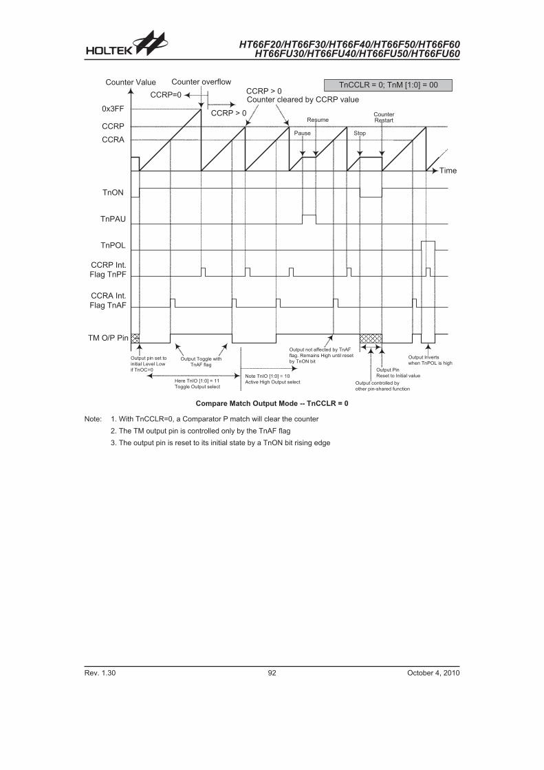
HT66F20/HT66F30/HT66F40/HT66F50/HT66F60HT66FU30/HT66FU40/HT66FU50/HT66FU60
Rev. 1.30 92 October 4, 2010
Counter Value
0x3FF
CCRP
CCRA
TnON
TnPAU
TnPOL
CCRP Int.
Flag TnPF
CCRA Int.
Flag TnAF
TM O/P Pin
Time
CCRP=0
CCRP > 0
Counter overflow
CCRP > 0Counter cleared by CCRP value
Pause
Resume
Stop
CounterRestart
TnCCLR = 0; TnM [1:0] = 00
Output pin set to
initial Level Low
if TnOC=0
Output Toggle with
TnAF flag
Note TnIO [1:0] = 10
Active High Output selectHere TnIO [1:0] = 11
Toggle Output select
Output not affected by TnAF
flag. Remains High until reset
by TnON bit
Output Pin
Reset to Initial value
Output controlled by
other pin-shared function
Output Inverts
when TnPOL is high
Compare Match Output Mode -- TnCCLR = 0
Note: 1. With TnCCLR=0, a Comparator P match will clear the counter
2. The TM output pin is controlled only by the TnAF flag
3. The output pin is reset to its initial state by a TnON bit rising edge

HT66F20/HT66F30/HT66F40/HT66F50/HT66F60HT66FU30/HT66FU40/HT66FU50/HT66FU60
Rev. 1.30 93 October 4, 2010
Counter Value
0x3FF
CCRP
CCRA
TnON
TnPAU
TnPOL
CCRP Int.
Flag TnPF
CCRA Int.
Flag TnAF
TM O/P Pin
Time
CCRA=0
CCRA = 0Counter overflow
CCRA > 0 Counter cleared by CCRA value
Pause
Resume
Stop Counter Restart
TnCCLR = 1; TnM [1:0] = 00
Output pin set to
initial Level Low
if TnOC=0
Output Toggle with
TnAF flag
Note TnIO [1:0] = 10
Active High Output selectHere TnIO [1:0] = 11
Toggle Output select
Output not affected by
TnAF flag. Remains High
until reset by TnON bitOutput Pin
Reset to Initial value
Output controlled by
other pin-shared function
Output Inverts
when TnPOL is high
TnPF notgenerated
No TnAF flaggenerated onCCRA overflow
Output doesnot change
Compare Match Output Mode -- TnCCLR = 1
Note: 1. With TnCCLR=1, a Comparator A match will clear the counter
2. The TM output pin is controlled only by the TnAF flag
3. The output pin is reset to its initial state by a TnON bit rising edge
4. The TnPF flag is not generated when TnCCLR=1

HT66F20/HT66F30/HT66F40/HT66F50/HT66F60HT66FU30/HT66FU40/HT66FU50/HT66FU60
Rev. 1.30 94 October 4, 2010
PWM Output Mode
To select this mode, bits TnM1 and TnM0 in the TMnC1
register should be set to 10 respectively. The PWM func-
tion within the TM is useful for applications which require
functions such as motor control, heating control, illumi-
nation control etc. By providing a signal of fixed fre-
quency but of varying duty cycle on the TM output pin, a
square wave AC waveform can be generated with vary-
ing equivalent DC RMS values.
As both the period and duty cycle of the PWM waveform
can be controlled, the choice of generated waveform is
extremely flexible. In the PWM mode, the TnCCLR bit
has no effect on the PWM operation. Both of the CCRA
and CCRP registers are used to generate the PWM
waveform, one register is used to clear the internal
counter and thus control the PWM waveform frequency,
while the other one is used to control the duty cycle.
Which register is used to control either frequency or duty
cycle is determined using the TnDPX bit in the TMnC1
register. The PWM waveform frequency and duty cycle
can therefore be controlled by the values in the CCRA
and CCRP registers.
An interrupt flag, one for each of the CCRA and CCRP,
will be generated when a compare match occurs from
either Comparator A or Comparator P. The TnOC bit in
the TMnC1 register is used to select the required polar-
ity of the PWM waveform while the two TnIO1 and
TnIO0 bits are used to enable the PWM output or to
force the TM output pin to a fixed high or low level. The
TnPOL bit is used to reverse the polarity of the PWM
output waveform.
Counter Value
CCRP
CCRA
TnON
TnPAU
TnPOL
CCRP Int.
Flag TnPF
CCRA Int.
Flag TnAF
TM O/P Pin(TnOC=1)
Time
Counter clearedby CCRP
Pause ResumeCounter Stop if
TnON bit low
Counter Reset whenTnON returns high
TnDPX = 0; TnM [1:0] = 10
PWM Duty Cycle
set by CCRA
PWM resumes
operationOutput controlled by
other pin-shared function Output Inverts
when TnPOL = 1PWM Period
set by CCRP
TM O/P Pin(TnOC=0)
PWM Mode -- TnDPX = 0
Note: 1. Here TnDPX=0 -- Counter cleared by CCRP
2. A counter clear sets the PWM Period
3. The internal PWM function continues even when TnIO [1:0] = 00 or 01
4. The TnCCLR bit has no influence on PWM operation

HT66F20/HT66F30/HT66F40/HT66F50/HT66F60HT66FU30/HT66FU40/HT66FU50/HT66FU60
Rev. 1.30 95 October 4, 2010
� CTM, PWM Mode, Edge-aligned Mode, T0DPX=0
CCRP 001b 010b 011b 100b 101b 110b 111b 000b
Period 128 256 384 512 640 768 896 1024
Duty CCRA
If fSYS = 16MHz, TM clock source is fSYS/4, CCRP = 100b and CCRA =128,
The CTM PWM output frequency = (fSYS/4) / 512 = fSYS/2048 = 7.8125 kHz, duty = 128/512 = 25%.
If the Duty value defined by the CCRA register is equal to or greater than the Period value, then the PWM output duty
is 100%.
� CTM, PWM Mode, Edge-aligned Mode, T0DPX=1
CCRP 001b 010b 011b 100b 101b 110b 111b 000b
Period CCRA
Duty 128 256 384 512 640 768 896 1024
The PWM output period is determined by the CCRA register value together with the TM clock while the PWM duty cy-
cle is defined by the CCRP register value.
Counter Value
CCRP
CCRA
TnON
TnPAU
TnPOL
CCRP Int.
Flag TnPF
CCRA Int.
Flag TnAF
TM O/P Pin(TnOC=1)
Time
Counter clearedby CCRA
Pause ResumeCounter Stop if
TnON bit low
Counter Reset whenTnON returns high
TnDPX = 1; TnM [1:0] = 10
PWM Duty Cycle
set by CCRP
PWM resumes
operationOutput controlled by
other pin-shared function Output Inverts
when TnPOL = 1PWM Period
set by CCRA
TM O/P Pin(TnOC=0)
PWM Mode -- TnDPX = 1
Note: 1. Here TnDPX = 1 -- Counter cleared by CCRA
2. A counter clear sets the PWM Period
3. The internal PWM function continues even when TnIO [1:0] = 00 or 01
4. The TnCCLR bit has no influence on PWM operation

HT66F20/HT66F30/HT66F40/HT66F50/HT66F60HT66FU30/HT66FU40/HT66FU50/HT66FU60
Rev. 1.30 96 October 4, 2010
Standard Type TM - STM
The Standard Type TM contains five operating modes, which are Compare Match Output, Timer/Event Counter, Cap-
ture Input, Single Pulse Output and PWM Output modes. The Standard TM can also be controlled with an external in-
put pin and can drive one or two external output pins.
CTM Name TM No. TM Input Pin TM Output Pin
HT66F20 10-bit STM 1 TCK1 TP1_0, TP1_1
HT66F30 � � � �
HT66F40 16-bit STM 2 TCK2 TP2_0, TP2_1
HT66F50 16-bit STM 2 TCK2 TP2_0, TP2_1
HT66F60 16-bit STM 2 TCK2 TP2_0, TP2_1
� � � �
� � � �
� � � � �
� � ! � � � � � � � � � � " � � � #
� � ! � � � � � � � � � � � " � � � #
� � � � � $ � � � � �
� � %
� � � � &
' ( $ ' ) � � � � ' 6 $ ' � �
� � � � � 6 � * ' � � � � � ! � � � � � � � � �
� � � � � � � 2 � * ' � �� � ! � � � � � � � � �
� � � � � � � � + � � �� � � � � � � 2 * ' � � � � � � � * � � � � � � � �
� � � � � � � � � � � �
� � � � � � � � � � � �
� � � � � � �� � � � � � � �
' � $ ' ) � � �' � $ ' � � �
7 5 8 �� � � � � � � �
� � � � , � � � � �
� � " � , � � � " �� � � � , � � � � �
� � �
� � �
� � + � � � � -� � � � � � +
� � �� � � � � � +
� � � � �
� � � � �
� � � � � � �
� � �
� � �
� � �
� � �
� � �
� � �
� � �
. / 0 / � �
. / 0 /
. 1 � � 2
. 1 � 2 �
. � � �
� � 3 � � 4 � 5
�
�
Standard Type TM Block Diagram
Standard TM Operation
There are two sizes of Standard TMs, one is 10-bits
wide and the other is 16-bits wide. At the core is a 10 or
16-bit count-up counter which is driven by a user
selectable internal or external clock source. There are
also two internal comparators with the names, Com-
parator A and Comparator P. These comparators will
compare the value in the counter with CCRP and CCRA
registers. The CCRP comparator is 3 or 8-bits wide
whose value is compared the with highest 3 or 8 bits in
the counter while the CCRA is the ten or sixteen bits and
therefore compares all counter bits.
The only way of changing the value of the 10 or 16-bit
counter using the application program, is to clear the
counter by changing the TnON bit from low to high. The
counter will also be cleared automatically by a counter
overflow or a compare match with one of its associated
comparators. When these conditions occur, a TM inter-
rupt signal will also usually be generated. The Standard
Type TM can operate in a number of different opera-
tional modes, can be driven by different clock sources
including an input pin and can also control an output pin.
All operating setup conditions are selected using rele-
vant internal registers.
Standard Type TM Register Description
Overall operation of the Standard TM is controlled using
a series of registers. A read only register pair exists to
store the internal counter 10 or 16-bit value, while a
read/write register pair exists to store the internal 10 or
16-bit CCRA value. The remaining two registers are
control registers which setup the different operating and
control modes as well as the three or eight CCRP bits.

HT66F20/HT66F30/HT66F40/HT66F50/HT66F60HT66FU30/HT66FU40/HT66FU50/HT66FU60
Rev. 1.30 97 October 4, 2010
Name Bit7 Bit6 Bit5 Bit4 Bit3 Bit2 Bit1 Bit0
TM1C0 T1PAU T1CK2 T1CK1 T1CK0 T1ON T1RP2 T1RP1 T1RP0
TM1C1 T1M1 T1M0 T1IO1 T1IO0 T1OC T1POL T1DPX T1CCLR
TM1DL D7 D6 D5 D4 D3 D2 D1 D0
TM1DH � � � � � � D9 D8
TM1AL D7 D6 D5 D4 D3 D2 D1 D0
TM1AH � � � � � � D9 D8
10-bit Standard TM Register List (for HT66F20)
Name Bit7 Bit6 Bit5 Bit4 Bit3 Bit2 Bit1 Bit0
TM2C0 T2PAU T2CK2 T2CK1 T2CK0 T2ON � � �
TM2C1 T2M1 T2M0 T2IO1 T2IO0 T2OC T2POL T2DPX T2CCLR
TM2DL D7 D6 D5 D4 D3 D2 D1 D0
TM2DH D15 D14 D13 D12 D11 D10 D9 D8
TM2AL D7 D6 D5 D4 D3 D2 D1 D0
TM2AH D15 D14 D13 D12 D11 D10 D9 D8
TM2RP D7 D6 D5 D4 D3 D2 D1 D0
16-bit Standard TM Register List (for HT66F40/HT66F50/HT66F60)
� 10-bit Standard TM Register List - HT66F20
� TM1C0 Register - 10-bit STM
Bit 7 6 5 4 3 2 1 0
Name T1PAU T1CK2 T1CK1 T1CK0 T1ON T1RP2 T1RP1 T1RP0
R/W R/W R/W R/W R/W R/W R/W R/W R/W
POR 0 0 0 0 0 0 0 0
Bit 7 T1PAU: TM1 Counter Pause Control
0: run
1: pause
The counter can be paused by setting this bit high. Clearing the bit to zero restores normal
counter operation. When in a Pause condition the TM will remain powered up and continue to
consume power. The counter will retain its residual value when this bit changes from low to high
and resume counting from this value when the bit changes to a low value again.
Bit 6~4 T1CK2~T1CK0: Select TM1 Counter clock
000: fSYS/4
001: fSYS
010: fH/16
011: fH/64
100: fTBC
101: undefined
110: TCK1 rising edge clock
111: TCK1 falling edge clock
These three bits are used to select the clock source for the TM. Selecting the Reserved clock
input will effectively disable the internal counter. The external pin clock source can be chosen to
be active on the rising or falling edge. The clock source fSYS is the system clock, while fH and
fTBC are other internal clocks, the details of which can be found in the oscillator section.

HT66F20/HT66F30/HT66F40/HT66F50/HT66F60HT66FU30/HT66FU40/HT66FU50/HT66FU60
Rev. 1.30 98 October 4, 2010
Bit 3 T1ON: TM1 Counter On/Off Control
0: Off
1: On
This bit controls the overall on/off function of the TM. Setting the bit high enables the counter to
run, clearing the bit disables the TM. Clearing this bit to zero will stop the counter from counting
and turn off the TM which will reduce its power consumption. When the bit changes state from
low to high the internal counter value will be reset to zero, however when the bit changes from
high to low, the internal counter will retain its residual value until the bit returns high again.
If the TM is in the Compare Match Output Mode then the TM output pin will be reset to its initial
condition, as specified by the T1OC bit, when the T1ON bit changes from low to high.
Bit 2~0 T1RP2~T1RP0: TM1 CCRP 3-bit register, compared with the TM1 Counter bit 9~bit 7
Comparator P Match Period
000: 1024 TM1 clocks
001: 128 TM1 clocks
010: 256 TM1 clocks
011: 384 TM1 clocks
100: 512 TM1 clocks
101: 640 TM1 clocks
110: 768 TM1 clocks
111: 896 TM1 clocks
These three bits are used to setup the value on the internal CCRP 3-bit register, which are then
compared with the internal counter's highest three bits. The result of this comparison can be
selected to clear the internal counter if the T1CCLR bit is set to zero. Setting the T1CCLR bit to
zero ensures that a compare match with the CCRP values will reset the internal counter. As the
CCRP bits are only compared with the highest three counter bits, the compare values exist in 128
clock cycle multiples. Clearing all three bits to zero is in effect allowing the counter to overflow at
its maximum value.
� TM1C1 Register - 10-bit STM
Bit 7 6 5 4 3 2 1 0
Name T1M1 T1M0 T1IO1 T1IO0 T1OC T1POL T1DPX T1CCLR
R/W R/W R/W R/W R/W R/W R/W R/W R/W
POR 0 0 0 0 0 0 0 0
Bit 7~6 T1M1~T1M0: Select TM1 Operating Mode
00: Compare Match Output Mode
01: Capture Input Mode
10: PWM Mode or Single Pulse Output Mode
11: Timer/Counter Mode
These bits setup the required operating mode for the TM. To ensure reliable operation the TM
should be switched off before any changes are made to the T1M1 and T1M0 bits. In the
Timer/Counter Mode, the TM output pin control must be disabled.
Bit 5~4 T1IO1~T1IO0: Select TP1_0, TP1_1 output function
Compare Match Output Mode
00: No change
01: Output low
10: Output high
11: Toggle output
PWM Mode/Single Pulse Output Mode
00: PWM output inactive state
01: PWM output active state
10: PWM output
11: Single pulse output
Capture Input Mode
00: Input capture at rising edge of TP1_0, TP1_1
01: Input capture at falling edge of TP1_0, TP1_1
10: Input capture at falling/rising edge of TP1_0, TP1_1
11: Input capture disabled
Timer/counter Mode:
Unused

HT66F20/HT66F30/HT66F40/HT66F50/HT66F60HT66FU30/HT66FU40/HT66FU50/HT66FU60
Rev. 1.30 99 October 4, 2010
These two bits are used to determine how the TM output pin changes state when a certain
condition is reached. The function that these bits select depends upon in which mode the TM is
running.
In the Compare Match Output Mode, the T1IO1 and T1IO0 bits determine how the TM output
pin changes state when a compare match occurs from the Comparator A. The TM output pin can
be setup to switch high, switch low or to toggle its present state when a compare match occurs
from the Comparator A. When the bits are both zero, then no change will take place on the
output. The initial value of the TM output pin should be setup using the T1OC bit in the TM1C1
register. Note that the output level requested by the T1IO1 and T1IO0 bits must be different from
the initial value setup using the T1OC bit otherwise no change will occur on the TM output pin
when a compare match occurs. After the TM output pin changes state it can be reset to its initial
level by changing the level of the T1ON bit from low to high.
In the PWM Mode, the T1IO1 and T1IO0 bits determine how the TM output pin changes state
when a certain compare match condition occurs. The PWM output function is modified by
changing these two bits. It is necessary to change the values of the T1IO1 and T1IO0 bits only
after the TM has been switched off. Unpredictable PWM outputs will occur if the T1IO1 and
T1IO0 bits are changed when the TM is running
Bit 3 T1OC: TP1_0, TP1_1 Output control bit
Compare Match Output Mode
0: initial low
1: initial high
PWM Mode/ Single Pulse Output Mode
0: Active low
1: Active high
This is the output control bit for the TM output pin. Its operation depends upon whether TM is
being used in the Compare Match Output Mode or in the PWM Mode/ Single Pulse Output Mode.
It has no effect if the TM is in the Timer/Counter Mode. In the Compare Match Output Mode it
determines the logic level of the TM output pin before a compare match occurs. In the PWM
Mode it determines if the PWM signal is active high or active low.
Bit 2 T1POL: TP1_0, TP1_1 Output polarity Control
0: non-invert
1: invert
This bit controls the polarity of the TP1_0 or TP1_1 output pin. When the bit is set high the TM
output pin will be inverted and not inverted when the bit is zero. It has no effect if the TM is in the
Timer/Counter Mode.
Bit 1 T1DPX: TM1 PWM period/duty Control
0: CCRP - period; CCRA - duty
1: CCRP - duty; CCRA - period
This bit, determines which of the CCRA and CCRP registers are used for period and duty
control of the PWM waveform.
Bit 0 T1CCLR: Select TM1 Counter clear condition
0: TM1 Comparatror P match
1: TM1 Comparatror A match
This bit is used to select the method which clears the counter. Remember that the Standard
TM contains two comparators, Comparator A and Comparator P, either of which can be selected
to clear the internal counter. With the T1CCLR bit set high, the counter will be cleared when a
compare match occurs from the Comparator A. When the bit is low, the counter will be cleared
when a compare match occurs from the Comparator P or with a counter overflow. A counter
overflow clearing method can only be implemented if the CCRP bits are all cleared to zero. The
T1CCLR bit is not used in the PWM, Single Pulse or Input Capture Mode.

HT66F20/HT66F30/HT66F40/HT66F50/HT66F60HT66FU30/HT66FU40/HT66FU50/HT66FU60
Rev. 1.30 100 October 4, 2010
� TM1DL Register - 10-bit STM
Bit 7 6 5 4 3 2 1 0
Name D7 D6 D5 D4 D3 D2 D1 D0
R/W R R R R R R R R
POR 0 0 0 0 0 0 0 0
Bit 7~0 TM1DL: TM1 Counter Low Byte Register bit 7~bit 0
TM1 10-bit Counter bit 7~bit 0
� TM1DH Register - 10-bit STM
Bit 7 6 5 4 3 2 1 0
Name � � � � � � D9 D8
R/W � � � � � � R R
POR � � � � � � 0 0
Bit 7~2 Unimplemented, read as �0�
Bit 1~0 TM1DH: TM1 Counter High Byte Register bit 1~bit 0
TM1 10-bit Counter bit 9~bit 8
� TM1AL Register - 10-bit STM
Bit 7 6 5 4 3 2 1 0
Name D7 D6 D5 D4 D3 D2 D1 D0
R/W R/W R/W R/W R/W R/W R/W R/W R/W
POR 0 0 0 0 0 0 0 0
Bit 7~0 TM1AL: TM1 CCRA Low Byte Register bit 7~bit 0
TM1 10-bit CCRA bit 7~bit 0
� TM1AH Register - 10-bit STM
Bit 7 6 5 4 3 2 1 0
Name � � � � � � D9 D8
R/W � � � � � � R/W R/W
POR � � � � � � 0 0
Bit 7~2 Unimplemented, read as �0�
Bit 1~0 TM1AH: TM1 CCRA High Byte Register bit 1~bit 0
TM1 10-bit CCRA bit 9~bit 8

HT66F20/HT66F30/HT66F40/HT66F50/HT66F60HT66FU30/HT66FU40/HT66FU50/HT66FU60
Rev. 1.30 101 October 4, 2010
� 16-bit Standard TM Register List - HT66F40/HT66F50/HT66F60
� TM2C0 Register - 16-bit STM
Bit 7 6 5 4 3 2 1 0
Name T2PAU T2CK2 T2CK1 T2CK0 T2ON � � �
R/W R/W R/W R/W R/W R/W � � �
POR 0 0 0 0 0 � � �
Bit 7 T2PAU: TM2 Counter Pause Control
0: Run
1: Pause
The counter can be paused by setting this bit high. Clearing the bit to zero restores normal
counter operation. When in a Pause condition the TM will remain powered up and continue to
consume power. The counter will retain its residual value when this bit changes from low to high
and resume counting from this value when the bit changes to a low value again.
Bit 6~4 T2CK2, T2CK1, T2CK0: Select TM2 Counter clock
000: fSYS/4
001: fSYS
010: fH/16
011: fH/64
100: fTBC
101: undefined
110: TCK2 rising edge clock
111: TCK2 falling edge clock
These three bits are used to select the clock source for the TM. Selecting the Reserved clock
input will effectively disable the internal counter. The external pin clock source can be chosen to
be active on the rising or falling edge. The clock source fSYS is the system clock, while fH and
fTBC are other internal clocks, the details of which can be found in the oscillator section.
Bit 3 T2ON: TM2 Counter On/Off Control
0: Off
1: On
This bit controls the overall on/off function of the TM. Setting the bit high enables the counter to
run, clearing the bit disables the TM. Clearing this bit to zero will stop the counter from counting
and turn off the TM which will reduce its power consumption. When the bit changes state from
low to high the internal counter value will be reset to zero, however when the bit changes from
high to low, the internal counter will retain its residual value until the bit returns high again.
If the TM is in the Compare Match Output Mode then the TM output pin will be reset to its initial
condition, as specified by the T2OC bit, when the T2ON bit changes from low to high.
Bit 2~0 Unimplemented, read as �0�

HT66F20/HT66F30/HT66F40/HT66F50/HT66F60HT66FU30/HT66FU40/HT66FU50/HT66FU60
Rev. 1.30 102 October 4, 2010
� TM2C1 Register - 16-bit STM
Bit 7 6 5 4 3 2 1 0
Name T2M1 T2M0 T2IO1 T2IO0 T2OC T2POL T2DPX T2CCLR
R/W R/W R/W R/W R/W R/W R/W R/W R/W
POR 0 0 0 0 0 0 0 0
Bit 7~6 T2M1~T2M0: Select TM2 Operating Mode
00: Compare Match Output Mode
01: Capture Input Mode
10: PWM Mode or Single Pulse Output Mode
11: Timer/Counter Mode
These bits setup the required operating mode for the TM. To ensure reliable operation the TM
should be switched off before any changes are made to the T2M1 and T2M0 bits. In the
Timer/Counter Mode, the TM output pin control must be disabled.
Bit 5~4 T2IO1~T2IO0: Select TP2_0, TP2_1 output function
Compare Match Output Mode
00: No change
01: Output low
10: Output high
11: Toggle output
PWM Mode/ Single Pulse Output Mode
00: PWM output inactive state
01: PWM output active state
10: PWM output
11: Single pulse output
Capture Input Mode
00: Input capture at rising edge of TP2_0, TP2_1
01: Input capture at falling edge of TP2_0, TP2_1
10: Input capture at falling/rising edge of TP2_0, TP2_1
11: Input capture disabled
Timer/counter Mode:
Unused
These two bits are used to determine how the TM output pin changes state when a certain
condition is reached. The function that these bits select depends upon in which mode the TM
is running.
In the Compare Match Output Mode, the T2IO1 and T2IO0 bits determine how the TM output
pin changes state when a compare match occurs from the Comparator A. The TM output pin can
be setup to switch high, switch low or to toggle its present state when a compare match occurs
from the Comparator A. When the bits are both zero, then no change will take place on the
output. The initial value of the TM output pin should be setup using the T2OC bit in the TM2C1
register. Note that the output level requested by the T2IO1 and T2IO0 bits must be different from
the initial value setup using the T2OC bit otherwise no change will occur on the TM output pin
when a compare match occurs. After the TM output pin changes state it can be reset to its initial
level by changing the level of the T2ON bit from low to high.
In the PWM Mode, the T2IO1 and T2IO0 bits determine how the TM output pin changes state
when a certain compare match condition occurs. The PWM output function is modified by
changing these two bits. It is necessary to change the values of the T2IO1 and T2IO0 bits only
after the TM has been switched off. Unpredictable PWM outputs will occur if the T2IO1 and
T2IO0 bits are changed when the TM is running
Bit 3 T2OC: TP2_0, TP2_1 Output control bit
Compare Match Output Mode
0: Initial low
1: Initial high
PWM Mode/ Single Pulse Output Mode
0: Active low
1: Active high
HT66F20/HT66F30/HT66F40/HT66F50/HT66F60HT66FU30/HT66FU40/HT66FU50/HT66FU60
Rev. 1.30 103 October 4, 2010
This is the output control bit for the TM output pin. Its operation depends upon whether TM is
being used in the Compare Match Output Mode or in the PWM Mode/ Single Pulse Output Mode.
It has no effect if the TM is in the Timer/Counter Mode. In the Compare Match Output Mode it
determines the logic level of the TM output pin before a compare match occurs. In the PWM
Mode it determines if the PWM signal is active high or active low.
Bit 2 T2POL: TP2_0, TP2_1 Output polarity Control
0: Non-invert
1: Invert
This bit controls the polarity of the TP2_0 or TP2_1 output pin. When the bit is set high the TM
output pin will be inverted and not inverted when the bit is zero. It has no effect if the TM is in the
Timer/Counter Mode.
Bit 1 T2DPX: TM2 PWM period/duty Control
0: CCRP - period; CCRA - duty
1: CCRP - duty; CCRA - period
This bit, determines which of the CCRA and CCRP registers are used for period and duty
control of the PWM waveform.
Bit 0 T2CCLR: Select TM2 Counter clear condition
0: TM2 Comparator P match
1: TM2 Comparator A match
This bit is used to select the method which clears the counter. Remember that the Standard
TM contains two comparators, Comparator A and Comparator P, either of which can be selected
to clear the internal counter. With the T2CCLR bit set high, the counter will be cleared when a
compare match occurs from the Comparator A. When the bit is low, the counter will be cleared
when a compare match occurs from the Comparator P or with a counter overflow. A counter
overflow clearing method can only be implemented if the CCRP bits are all cleared to zero.
The T1CCLR bit is not used in the PWM, Single Pulse or Input Capture Mode.
� TM2DL Register - 16-bit STM
Bit 7 6 5 4 3 2 1 0
Name D7 D6 D5 D4 D3 D2 D1 D0
R/W R R R R R R R R
POR 0 0 0 0 0 0 0 0
Bit 7~0 TM2DL: TM2 Counter Low Byte Register bit 7~bit 0
TM2 16-bit Counter bit 7~bit 0
� TM2DH Register - 16-bit STM
Bit 7 6 5 4 3 2 1 0
Name D15 D14 D13 D12 D11 D10 D9 D8
R/W R R R R R R R R
POR 0 0 0 0 0 0 0 0
Bit 7~0 TM2DH: TM2 Counter High Byte Register bit 7~bit 0
TM2 16-bit Counter bit 15~bit 8
� TM2AL Register - 16-bit STM
Bit 7 6 5 4 3 2 1 0
Name D7 D6 D5 D4 D3 D2 D1 D0
R/W R/W R/W R/W R/W R/W R/W R/W R/W
POR 0 0 0 0 0 0 0 0
Bit 7~0 TM2AL: TM2 CCRA Low Byte Register bit 7~bit 0
TM2 16-bit CCRA bit 7~bit 0

HT66F20/HT66F30/HT66F40/HT66F50/HT66F60HT66FU30/HT66FU40/HT66FU50/HT66FU60
Rev. 1.30 104 October 4, 2010
� TM2AH Register - 16-bit STM
Bit 7 6 5 4 3 2 1 0
Name D15 D14 D13 D12 D11 D10 D9 D8
R/W R/W R/W R/W R/W R/W R/W R/W R/W
POR 0 0 0 0 0 0 0 0
Bit 7~0 TM2AH: TM2 CCRA High Byte Register bit 7~bit 0
TM2 16-bit CCRA bit 15~bit 8
� TM2RP Register - 16-bit STM
Bit 7 6 5 4 3 2 1 0
Name D7 D6 D5 D4 D3 D2 D1 D0
R/W R/W R/W R/W R/W R/W R/W R/W R/W
POR 0 0 0 0 0 0 0 0
Bit 7~0 TM2RP: TM2 CCRP Register bit 7 ~ bit 0
TM2 CCRP 8-bit register, compared with the TM2 Counter bit 15 ~ bit 8. Comparator P Match
Period
0: 65536 TM2 clocks
1~255: 256 x (1~255) TM2 clocks
These eight bits are used to setup the value on the internal CCRP 8-bit register, which are then
compared with the internal counter's highest eight bits. The result of this comparison can be
selected to clear the internal counter if the T2CCLR bit is set to zero. Setting the T2CCLR bit to
zero ensures that a compare match with the CCRP values will reset the internal counter. As the
CCRP bits are only compared with the highest eight counter bits, the compare values exist in 256
clock cycle multiples. Clearing all eight bits to zero is in effect allowing the counter to overflow at
its maximum value.
Standard Type TM Operating Modes
The Standard Type TM can operate in one of five oper-
ating modes, Compare Match Output Mode, PWM Out-
put Mode, Single Pulse Output Mode, Capture Input
Mode or Timer/Counter Mode. The operating mode is
selected using the TnM1 and TnM0 bits in the TMnC1
register.
Compare Output Mode
To select this mode, bits TnM1 and TnM0 in the TMnC1
register, should be set to 00 respectively. In this mode
once the counter is enabled and running it can be
cleared by three methods. These are a counter over-
flow, a compare match from Comparator A and a com-
pare match from Comparator P. When the TnCCLR bit is
low, there are two ways in which the counter can be
cleared. One is when a compare match from Compara-
tor P, the other is when the CCRP bits are all zero which
allows the counter to overflow. Here both TnAF and
TnPF interrupt request flags for Comparator A and Com-
parator P respectively, will both be generated.
If the TnCCLR bit in the TMnC1 register is high then the
counter will be cleared when a compare match occurs
from Comparator A. However, here only the TnAF inter-
rupt request flag will be generated even if the value of
the CCRP bits is less than that of the CCRA registers.
Therefore when TnCCLR is high no TnPF interrupt re-
quest flag will be generated. In the Compare Match Out-
put Mode, the CCRA can not be set to �0�.
As the name of the mode suggests, after a comparison
is made, the TM output pin, will change state. The TM
output pin condition however only changes state when
an TnAF interrupt request flag is generated after a com-
pare match occurs from Comparator A. The TnPF inter-
rupt request flag, generated from a compare match
occurs from Comparator P, will have no effect on the TM
output pin. The way in which the TM output pin changes
state are determined by the condition of the TnIO1 and
TnIO0 bits in the TMnC1 register. The TM output pin can
be selected using the TnIO1 and TnIO0 bits to go high,
to go low or to toggle from its present condition when a
compare match occurs from Comparator A. The initial
condition of the TM output pin, which is setup after the
TnON bit changes from low to high, is setup using the
TnOC bit. Note that if the TnIO1 and TnIO0 bits are zero
then no pin change will take place.
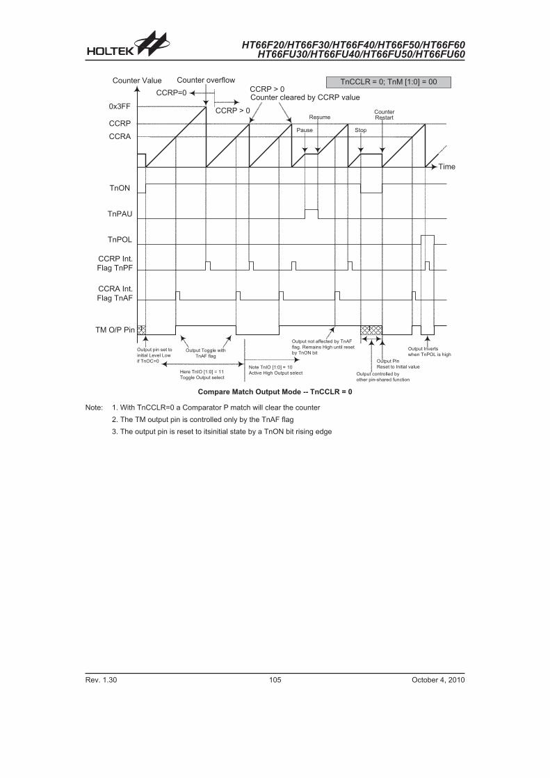
HT66F20/HT66F30/HT66F40/HT66F50/HT66F60HT66FU30/HT66FU40/HT66FU50/HT66FU60
Rev. 1.30 105 October 4, 2010
Counter Value
0x3FF
CCRP
CCRA
TnON
TnPAU
TnPOL
CCRP Int.
Flag TnPF
CCRA Int.
Flag TnAF
TM O/P Pin
Time
CCRP=0
CCRP > 0
Counter overflow
CCRP > 0Counter cleared by CCRP value
Pause
Resume
Stop
CounterRestart
TnCCLR = 0; TnM [1:0] = 00
Output pin set to
initial Level Low
if TnOC=0
Output Toggle with
TnAF flag
Note TnIO [1:0] = 10
Active High Output selectHere TnIO [1:0] = 11
Toggle Output select
Output not affected by TnAF
flag. Remains High until reset
by TnON bit
Output Pin
Reset to Initial value
Output controlled by
other pin-shared function
Output Inverts
when TnPOL is high
Compare Match Output Mode -- TnCCLR = 0
Note: 1. With TnCCLR=0 a Comparator P match will clear the counter
2. The TM output pin is controlled only by the TnAF flag
3. The output pin is reset to itsinitial state by a TnON bit rising edge

HT66F20/HT66F30/HT66F40/HT66F50/HT66F60HT66FU30/HT66FU40/HT66FU50/HT66FU60
Rev. 1.30 106 October 4, 2010
Counter Value
0x3FF
CCRP
CCRA
TnON
TnPAU
TnPOL
CCRP Int.
Flag TnPF
CCRA Int.
Flag TnAF
TM O/P Pin
Time
CCRA=0
CCRA = 0Counter overflow
CCRA > 0 Counter cleared by CCRA value
Pause
Resume
Stop Counter Restart
TnCCLR = 1; TnM [1:0] = 00
Output pin set to
initial Level Low
if TnOC=0
Output Toggle with
TnAF flag
Note TnIO [1:0] = 10
Active High Output selectHere TnIO [1:0] = 11
Toggle Output select
Output not affected by
TnAF flag. Remains High
until reset by TnON bitOutput Pin
Reset to Initial value
Output controlled by
other pin-shared function
Output Inverts
when TnPOL is high
TnPF notgenerated
No TnAF flaggenerated onCCRA overflow
Output doesnot change
Compare Match Output Mode -- TnCCLR = 1
Note: 1. With TnCCLR=1 a Comparator A match will clear the counter
2. The TM output pin is controlled only by the TnAF flag
3. The output pin is reset to its initial state by a TnON bit rising edge
4. A TnPF flag is not generated when TnCCLR=1

HT66F20/HT66F30/HT66F40/HT66F50/HT66F60HT66FU30/HT66FU40/HT66FU50/HT66FU60
Rev. 1.30 107 October 4, 2010
Timer/Counter Mode
To select this mode, bits TnM1 and TnM0 in the TMnC1
register should be set to 11 respectively. The
Timer/Counter Mode operates in an identical way to the
Compare Match Output Mode generating the same in-
terrupt flags. The exception is that in the Timer/Counter
Mode the TM output pin is not used. Therefore the
above description and Timing Diagrams for the Com-
pare Match Output Mode can be used to understand its
function. As the TM output pin is not used in this mode,
the pin can be used as a normal I/O pin or other
pin-shared function.
PWM Output Mode
To select this mode, bits TnM1 and TnM0 in the TMnC1
register should be set to 10 respectively and also the
TnIO1 and TnIO0 bits should be set to 10 respectively.
The PWM function within the TM is useful for applica-
tions which require functions such as motor control,
heating control, illumination control etc. By providing a
signal of fixed frequency but of varying duty cycle on the
TM output pin, a square wave AC waveform can be gen-
erated with varying equivalent DC RMS values.
As both the period and duty cycle of the PWM waveform
can be controlled, the choice of generated waveform is
extremely flexible. In the PWM mode, the TnCCLR bit
has no effect as the PWM period. Both of the CCRA and
CCRP registers are used to generate the PWM wave-
form, one register is used to clear the internal counter
and thus control the PWM waveform frequency, while
the other one is used to control the duty cycle. Which
register is used to control either frequency or duty cycle
is determined using the TnDPX bit in the TMnC1 regis-
ter. The PWM waveform frequency and duty cycle can
therefore be controlled by the values in the CCRA and
CCRP registers.
An interrupt flag, one for each of the CCRA and CCRP,
will be generated when a compare match occurs from
either Comparator A or Comparator P. The TnOC bit in
the TMnC1 register is used to select the required polar-
ity of the PWM waveform while the two TnIO1 and
TnIO0 bits are used to enable the PWM output or to
force the TM output pin to a fixed high or low level. The
TnPOL bit is used to reverse the polarity of the PWM
output waveform.
� 10-bit STM, PWM Mode, Edge-aligned Mode, T0DPX=0
CCRP 001b 010b 011b 100b 101b 110b 111b 000b
Period 128 256 384 512 640 768 896 1024
Duty CCRA
If fSYS = 16MHz, TM clock source is fSYS/4, CCRP = 100b and CCRA =128,
The STM PWM output frequency = (fSYS/4) / 512 = fSYS/2048 = 7.8125 kHz, duty = 128/512 = 25%.
If the Duty value defined by the CCRA register is equal to or greater than the Period value, then the PWM output duty
is 100%.
� 10-bit STM, PWM Mode, Edge-aligned Mode, T0DPX=1
CCRP 001b 010b 011b 100b 101b 110b 111b 000b
Period CCRA
Duty 128 256 384 512 640 768 896 1024
The PWM output period is determined by the CCRA register value together with the TM clock while the PWM duty cy-
cle is defined by the CCRP register value.

HT66F20/HT66F30/HT66F40/HT66F50/HT66F60HT66FU30/HT66FU40/HT66FU50/HT66FU60
Rev. 1.30 108 October 4, 2010
Counter Value
CCRP
CCRA
TnON
TnPAU
TnPOL
CCRP Int.
Flag TnPF
CCRA Int.
Flag TnAF
TM O/P Pin(TnOC=1)
Time
Counter clearedby CCRP
Pause ResumeCounter Stop if
TnON bit low
Counter Reset whenTnON returns high
TnDPX = 0; TnM [1:0] = 10
PWM Duty Cycle
set by CCRAPWM resumes
operationOutput controlled by
other pin-shared function Output Inverts
when TnPOL = 1PWM Period
set by CCRP
TM O/P Pin(TnOC=0)
PWM Mode -- TnDPX = 0
Note: 1. Here TnDPX=0 ¡V Counter cleared by CCRP
2. A counter clear sets the PWM Period
3. The internal PWM function continues running even when TnIO [1:0] = 00 or 01
4. The TnCCLR bit has no influence on PWM operation
� 10-bit STM, PWM Mode, Edge-aligned Mode, T0DPX=1
CCRP 1~255 000b
Period CCRP � 256 65536
Duty CCRA
If fSYS = 16MHz, TM clock source is fSYS/4, CCRP = 2 and CCRA =128,
The STM PWM output frequency = (fSYS/4) / (2�256) = fSYS/2048 = 7.8125 kHz, duty = 128 / (2�512) = 25%.
If the Duty value defined by the CCRA register is equal to or greater than the Period value, then the PWM output duty
is 100%.
� 16-bit STM, PWM Mode, Edge-aligned Mode, T0DPX=1
CCRP 001b 010b
Period CCRA
Duty CCRP � 256 65536
The PWM output period is determined by the CCRA register value together with the TM clock while the PWM duty cy-
cle is defined by the (CCRP x 256) except when the CCRP value is equal to 000b.
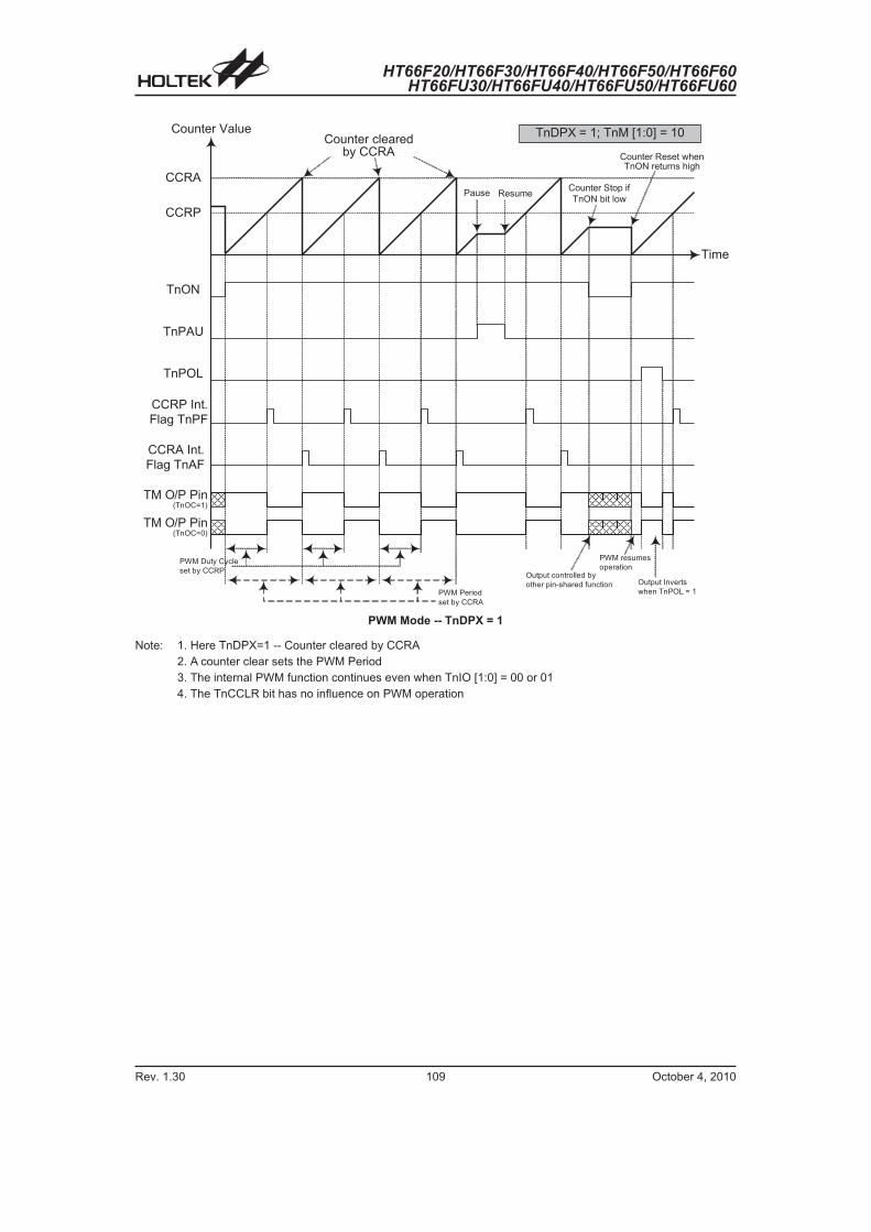
HT66F20/HT66F30/HT66F40/HT66F50/HT66F60HT66FU30/HT66FU40/HT66FU50/HT66FU60
Rev. 1.30 109 October 4, 2010
Counter Value
CCRP
CCRA
TnON
TnPAU
TnPOL
CCRP Int.
Flag TnPF
CCRA Int.
Flag TnAF
TM O/P Pin(TnOC=1)
Time
Counter clearedby CCRA
Pause ResumeCounter Stop if
TnON bit low
Counter Reset whenTnON returns high
TnDPX = 1; TnM [1:0] = 10
PWM Duty Cycle
set by CCRP
PWM resumes
operationOutput controlled by
other pin-shared function Output Inverts
when TnPOL = 1PWM Period
set by CCRA
TM O/P Pin(TnOC=0)
PWM Mode -- TnDPX = 1
Note: 1. Here TnDPX=1 -- Counter cleared by CCRA
2. A counter clear sets the PWM Period
3. The internal PWM function continues even when TnIO [1:0] = 00 or 01
4. The TnCCLR bit has no influence on PWM operation

HT66F20/HT66F30/HT66F40/HT66F50/HT66F60HT66FU30/HT66FU40/HT66FU50/HT66FU60
Rev. 1.30 110 October 4, 2010
Single Pulse Mode
To select this mode, bits TnM1 and TnM0 in the TMnC1
register should be set to 10 respectively and also the
TnIO1 and TnIO0 bits should be set to 11 respectively.
The Single Pulse Output Mode, as the name suggests,
will generate a single shot pulse on the TM output pin.
The trigger for the pulse output leading edge is a low to
high transition of the TnON bit, which can be imple-
mented using the application program. However in the
Single Pulse Mode, the TnON bit can also be made to
automatically change from low to high using the external
TCKn pin, which will in turn initiate the Single Pulse out-
put. When the TnON bit transitions to a high level, the
counter will start running and the pulse leading edge will
be generated. The TnON bit should remain high when
the pulse is in its active state. The generated pulse trail-
ing edge will be generated when the TnON bit is cleared
to zero, which can be implemented using the application
program or when a compare match occurs from Com-
parator A.
� � 5 � � 8 � 7 5 8 �
� � % � ' � �
� � � � �
/ � 9 � � � ! ! � � 5
/ 7 � � : � � % :
� �
� � � � � � � � � � � � � 3 � � � � �
� � % � ' � �
� � � � �
/ � 9 � � � ! ! � � 5
� � � : � � % :
� �
� � � � � " � � � # � � � ! � � � �
� + 3 � � 9 � 5 � # � ; � � � � � � < � + �
� � � � + � � 8 � 7 5 8 �
� " � � � � � � � � �
Single Pulse Generation
Counter Value
CCRP
CCRA
TnON
TnPAU
TnPOL
CCRP Int.
Flag TnPF
CCRA Int.
Flag TnAF
TM O/P Pin(TnOC=1)
Time
Counter stoppedby CCRA
PauseResume Counter Stops
by software
Counter Reset whenTnON returns high
TnM [1:0] = 10 ; TnIO [1:0] = 11
Pulse Width
set by CCRA
Output Inverts
when TnPOL = 1
No CCRP Interruptsgenerated
TM O/P Pin(TnOC=0)
TCKn pin
SoftwareTrigger
Cleared byCCRA match
TCKn pinTrigger
Auto. set byTCKn pin
SoftwareTrigger
SoftwareClear
SoftwareTriggerSoftware
Trigger
Single Pulse Mode
Note: 1. Counter stopped by CCRA
2. CCRP is not used
3. The pulse is triggered by the TCKn pin or by setting the TnON bit high
4. A TCKn pin active edge will automatically set the TnON bit high
5. In the Single Pulse Mode, TnIO [1:0] must be set to �11� and can not be changed.

HT66F20/HT66F30/HT66F40/HT66F50/HT66F60HT66FU30/HT66FU40/HT66FU50/HT66FU60
Rev. 1.30 111 October 4, 2010
However a compare match from Comparator A will also
automatically clear the TnON bit and thus generate the
Single Pulse output trailing edge. In this way the CCRA
value can be used to control the pulse width. A compare
match from Comparator A will also generate a TM inter-
rupt. The counter can only be reset back to zero when
the TnON bit changes from low to high when the counter
restarts. In the Single Pulse Mode CCRP is not used.
The TnCCLR and TnDPX bits are not used in this Mode.
Capture Input Mode
To select this mode bits TnM1 and TnM0 in the TMnC1
register should be set to 01 respectively. This mode en-
ables external signals to capture and store the present
value of the internal counter and can therefore be used
for applications such as pulse width measurements.
The external signal is supplied on the TPn_0 or TPn_1
pin, whose active edge can be either a rising edge, a
falling edge or both rising and falling edges; the active
edge transition type is selected using the TnIO1 and
TnIO0 bits in the TMnC1 register. The counter is started
when the TnON bit changes from low to high which is ini-
tiated using the application program.
When the required edge transition appears on the
TPn_0 or TPn_1 pin the present value in the counter will
be latched into the CCRA registers and a TM interrupt
generated. Irrespective of what events occur on the
TPn_0 or TPn_1 pin the counter will continue to free run
until the TnON bit changes from high to low. When a
CCRP compare match occurs the counter will reset
back to zero; in this way the CCRP value can be used to
control the maximum counter value. When a CCRP
compare match occurs from Comparator P, a TM inter-
rupt will also be generated. Counting the number of
overflow interrupt signals from the CCRP can be a use-
ful method in measuring long pulse widths. The TnIO1
and TnIO0 bits can select the active trigger edge on the
TPn_0 or TPn_1 pin to be a rising edge, falling edge or
both edge types. If the TnIO1 and TnIO0 bits are both
set high, then no capture operation will take place irre-
spective of what happens on the TPn_0 or TPn_1 pin,
however it must be noted that the counter will continue
to run.
As the TPn_0 or TPn_1 pin is pin shared with other func-
tions, care must be taken if the TM is in the Input Cap-
ture Mode. This is because if the pin is setup as an
output, then any transitions on this pin may cause an in-
put capture operation to be executed. The TnCCLR and
TnDPX bits are not used in this Mode.
Counter Value
YY
CCRP
TnON
TnPAU
CCRP Int.
Flag TnPF
CCRA Int.
Flag TnAF
CCRAValue
Time
Counter clearedby CCRP
PauseResume
CounterReset
TnM [1:0] = 01
TM capture
pin TPn_x
XX
CounterStop
TnIO [1:0]Value
XX YY XX YY
Activeedge
Activeedge
Active edge
00 Rising edge 01 Falling edge 10 Both edges 11 Disable Capture
Capture Input Mode
Note: 1.. TnM [1:0] = 01 and active edge set by the TnIO [1:0] bits
2. A TM Capture input pin active edge transfers the counter value to CCRA
3. TnCCLR bit not used
4. No output function -- TnOC and TnPOL bits are not used
5. CCRP determines the counter value and the counter has a maximum count value when CCRP is equal to
zero.

HT66F20/HT66F30/HT66F40/HT66F50/HT66F60HT66FU30/HT66FU40/HT66FU50/HT66FU60
Rev. 1.30 112 October 4, 2010
Enhanced Type TM - ETM
The Enhanced Type TM contains five operating modes, which are Compare Match Output, Timer/Event Counter, Cap-
ture Input, Single Pulse Output and PWM Output modes. The Enhanced TM can also be controlled with an external in-
put pin and can drive three or four external output pins.
CTM Name TM No. TM Input Pin TM Output Pin
HT66F20 � � � �
HT66F30 10-bit ETM 1 TCK1 TP1A; TP1B_0, TP1B_1
HT66F40 10-bit ETM 1 TCK1 TP1A, TP1B_0, TP1B_1, TP1B_2
HT66F50 10-bit ETM 1 TCK1 TP1A, TP1B_0, TP1B_1, TP1B_2
HT66F60 10-bit ETM 1 TCK1 TP1A, TP1B_0, TP1B_1, TP1B_2
� � � �
� � � �
� � � � �
� � ! � � � � � � � � � � " � � � #
� � ! � � � � � � � � � � � " � � � #� � � � � $ � � � � �
� � %
� � � � &
' ( $ ' )
� * ' � � � � � ! � � � � � � � � �
� � * ' � �� � ! � � � � � � � � �
� � � � � �� + � � �
� � * ' � � � � & � � � � = � � � � � � � �
� � � � � � � � � � � �
� � � � � � � � � � �
� � � � � � � �� � � � � � � �
' � $ ' )
7 5 8 �� � � � � � � �
� � � � � , � � � � � �
� � � " � , � � � � " �� � � � � , � � � � � �
� � � �
� � � �
� � + � � � � -� � � � � � +
� � �� � � � � � +
� � � �
� � � � � � �
� � �
� � �
� � �
� � �
� � �
� � �
� � �
. / 0 / � �
. / 0 /
. 1 � � 2
. 1 � 2 �
. � � �
� � 3 � � 4 � 5
� � � � � � � � � � �
� � � � � � � �� � � � � � � �
� � � " � , � � � � " �� � � � � , � � � � � �
� � � �
� � � �
� � + � � � � -� � � � � � +
� � �� � � � � � +
� � � �
� � ! � � � � � � � � � � � " � � � #� � * ' � �� � ! � � � � � � � � �
7 5 8 �� � � � � � � �
� � � � , � � � � �
� � � � * �
� � � � * �
� � � � * �
�
�
Enhanced Type TM Block Diagram
Enhanced TM Operation
At its core is a 10-bit count-up/count-down counter
which is driven by a user selectable internal or external
clock source. There are three internal comparators with
the names, Comparator A, Comparator B and Com-
parator P. These comparators will compare the value in
the counter with the CCRA, CCRB and CCRP registers.
The CCRP comparator is 3-bits wide whose value is
compared with the highest 3-bits in the counter while
CCRA and CCRB are 10-bits wide and therefore com-
pared with all counter bits.
The only way of changing the value of the 10-bit counter
using the application program, is to clear the counter by
changing the TnON bit from low to high. The counter will
also be cleared automatically by a counter overflow or a
compare match with one of its associated comparators.
When these conditions occur, a TM interrupt signal will
also usually be generated. The Enhanced Type TM can
operate in a number of different operational modes, can
be driven by different clock sources including an input
pin and can also control output pins. All operating setup
conditions are selected using relevant internal registers.

HT66F20/HT66F30/HT66F40/HT66F50/HT66F60HT66FU30/HT66FU40/HT66FU50/HT66FU60
Rev. 1.30 113 October 4, 2010
Enhanced Type TM Register Description
Overall operation of the Enhanced TM is controlled using a series of registers. A read only register pair exists to store
the internal counter 10-bit value, while two read/write register pairs exist to store the internal 10-bit CCRA and CCRB
value. The remaining three registers are control registers which setup the different operating and control modes as well
as the three CCRP bits.
Name Bit7 Bit6 Bit5 Bit4 Bit3 Bit2 Bit1 Bit0
TM1C0 T1PAU T1CK2 T1CK1 T1CK0 T1ON T1RP2 T1RP1 T1RP0
TM1C1 T1AM1 T1AM0 T1AIO1 T1AIO0 T1AOC T1APOL T1CDN T1CCLR
TM1C2 T1BM1 T1BM0 T1BIO1 T1BIO0 T1BOC T1BPOL T1PWM1 T1PWM0
TM1DL D7 D6 D5 D4 D3 D2 D1 D0
TM1DH � � � � � � D9 D8
TM1AL D7 D6 D5 D4 D3 D2 D1 D0
TM1AH � � � � � � D9 D8
TM1BL D7 D6 D5 D4 D3 D2 D1 D0
TM1BH � � � � � � D9 D8
10-bit Enhanced TM Register List (if ETM is TM1)
� 10-bit Enhanced TM Register List - HT66F30/HT66F40/HT66F50/HT66F60
� TM1C0 Register - 10-bit ETM
Bit 7 6 5 4 3 2 1 0
Name T1PAU T1CK2 T1CK1 T1CK0 T1ON T1RP2 T1RP1 T1RP0
R/W R/W R/W R/W R/W R/W R/W R/W R/W
POR 0 0 0 0 0 0 0 0
Bit 7 T1PAU: TM1 Counter Pause Control
0: run
1: pause
The counter can be paused by setting this bit high. Clearing the bit to zero restores normal
counter operation. When in a Pause condition the TM will remain powered up and continue to
consume power. The counter will retain its residual value when this bit changes from low to high
and resume counting from this value when the bit changes to a low value again.
Bit 6~4 T1CK2~T1CK0: Select TM1 Counter clock
000: fSYS/4
001: fSYS
010: fH/16
011: fH/64
100: fTBC
101: Undefined
110: TCK1 rising edge clock
111: TCK1 falling edge clock
These three bits are used to select the clock source for the TM. Selecting the Reserved clock
input will effectively disable the internal counter. The external pin clock source can be chosen to
be active on the rising or falling edge. The clock source fSYS is the system clock, while fH and
fTBC are other internal clocks, the details of which can be found in the oscillator section.
Bit 3 T1ON: TM1 Counter On/Off Control
0: Off
1: On
This bit controls the overall on/off function of the TM. Setting the bit high enables the counter to
run, clearing the bit disables the TM. Clearing this bit to zero will stop the counter from counting
and turn off the TM which will reduce its power consumption. When the bit changes state from
low to high the internal counter value will be reset to zero, however when the bit changes from
high to low, the internal counter will retain its residual value until the bit returns high again.

HT66F20/HT66F30/HT66F40/HT66F50/HT66F60HT66FU30/HT66FU40/HT66FU50/HT66FU60
Rev. 1.30 114 October 4, 2010
If the TM is in the Compare Match Output Mode then the TM output pin will be reset to its initial
condition, as specified by the T1OC bit, when the T1ON bit changes from low to high.
Bit 2~0 T1RP2~T1RP0: TM1 CCRP 3-bit register, compared with the TM1 Counter bit 9~bit 7
Comparator P Match Period
000: 1024 TM1 clocks
001: 128 TM1 clocks
010: 256 TM1 clocks
011: 384 TM1 clocks
100: 512 TM1 clocks
101: 640 TM1 clocks
110: 768 TM1 clocks
111: 896 TM1 clocks
These three bits are used to setup the value on the internal CCRP 3-bit register, which are then
compared with the internal counter�s highest three bits. The result of this comparison can be
selected to clear the internal counter if the T1CCLR bit is set to zero. Setting the T1CCLR bit to
zero ensures that a compare match with the CCRP values will reset the internal counter. As the
CCRP bits are only compared with the highest three counter bits, the compare values exist in 128
clock cycle multiples. Clearing all three bits to zero is in effect allowing the counter to overflow at
its maximum value.
� TM1C1 Register - 10-bit ETM
Bit 7 6 5 4 3 2 1 0
Name T1AM1 T1AM0 T1AIO1 T1AIO0 T1AOC T1APOL T1CDN T1CCLR
R/W R/W R/W R/W R/W R/W R/W R R/W
POR 0 0 0 0 0 0 0 0
Bit 7~6 T1AM1~T1AM0: Select TM1 CCRA Operating Mode
00: Compare Match Output Mode
01: Capture Input Mode
10: PWM Mode or Single Pulse Output Mode
11: Timer/Counter Mode
These bits setup the required operating mode for the TM. To ensure reliable operation the TM
should be switched off before any changes are made to the T1AM1 and T1AM0 bits. In the
Timer/Counter Mode, the TM output pin control must be disabled.
Bit 5~4 T1AIO1~T1AIO0: Select TP1A output function
Compare Match Output Mode
00: No change
01: Output low
10: Output high
11: Toggle output
PWM Mode/ Single Pulse Output Mode
00: PWM output inactive state
01: PWM output active state
10: PWM output
11: Single pulse output
Capture Input Mode
00: Input capture at rising edge of TP1A
01: Input capture at falling edge of TP1A
10: Input capture at falling/rising edge of TP1A
11: Input capture disabled
Timer/counter Mode
Unused
These two bits are used to determine how the TM output pin changes state when a certain
condition is reached. The function that these bits select depends upon in which mode the TM is
running.
HT66F20/HT66F30/HT66F40/HT66F50/HT66F60HT66FU30/HT66FU40/HT66FU50/HT66FU60
Rev. 1.30 115 October 4, 2010
In the Compare Match Output Mode, the T1AIO1 and T1AIO0 bits determine how the TM
output pin changes state when a compare match occurs from the Comparator A. The TM output
pin can be setup to switch high, switch low or to toggle its present state when a compare match
occurs from the Comparator A. When the bits are both zero, then no change will take place on
the output. The initial value of the TM output pin should be setup using the T1AOC bit in the
TM1C1 register. Note that the output level requested by the T1AIO1 and T1AIO0 bits must be
different from the initial value setup using the T1AOC bit otherwise no change will occur on the
TM output pin when a compare match occurs. After the TM output pin changes state it can be
reset to its initial level by changing the level of the T1ON bit from low to high.
In the PWM Mode, the T1AIO1 and T1AIO0 bits determine how the TM output pin changes state
when a certain compare match condition occurs. The PWM output function is modified by
changing these two bits. It is necessary to change the values of the T1AIO1 and T1AIO0 bits
only after the TM has been switched off. Unpredictable PWM outputs will occur if the T1AIO1
and T1AIO0 bits are changed when the TM is running
Bit 3 T1AOC: TP1A Output control bit
Compare Match Output Mode
0: Initial low
1: Initial high
PWM Mode/ Single Pulse Output Mode
0: Active low
1: Active high
This is the output control bit for the TM output pin. Its operation depends upon whether TM is
being used in the Compare Match Output Mode or in the PWM Mode/ Single Pulse Output Mode.
It has no effect if the TM is in the Timer/Counter Mode. In the Compare Match Output Mode it
determines the logic level of the TM output pin before a compare match occurs. In the PWM
Mode it determines if the PWM signal is active high or active low.
Bit 2 T1APOL: TP1A Output polarity Control
0: Non-invert
1: Invert
This bit controls the polarity of the TP1A output pin. When the bit is set high the TM output pin
will be inverted and not inverted when the bit is zero. It has no effect if the TM is in the
Timer/Counter Mode.
Bit 1 T1CDN: TM1 Counter count up or down flag
0: Count up
1: Count down
Bit 0 T1CCLR: Select TM1 Counter clear condition
0: TM1 Comparator P match
1: TM1 Comparator A match
This bit is used to select the method which clears the counter. Remember that the Enhanced
TM contains three comparators, Comparator A, Comparator B and Comparator P, but only
Comparator A or Comparator Pan be selected to clear the internal counter. With the T1CCLR bit
set high, the counter will be cleared when a compare match occurs from the Comparator A.
When the bit is low, the counter will be cleared when a compare match occurs from the
Comparator P or with a counter overflow. A counter overflow clearing method can only be
implemented if the CCRP bits are all cleared to zero. The T1CCLR bit is not used in the PWM,
Single Pulse or Input Capture Mode.

HT66F20/HT66F30/HT66F40/HT66F50/HT66F60HT66FU30/HT66FU40/HT66FU50/HT66FU60
Rev. 1.30 116 October 4, 2010
� TM1C2 Register - 10-bit ETM
Bit 7 6 5 4 3 2 1 0
Name T1BM1 T1BM0 T1BIO1 T1BIO0 T1BOC T1BPOL T1PWM1 T1PWM0
R/W R/W R/W R/W R/W R/W R/W R R/W
POR 0 0 0 0 0 0 0 0
Bit 7~6 T1BM1~T1BM0: Select TM1 CCRB Operating Mode
00: Compare Match Output Mode
01: Capture Input Mode
10: PWM Mode or Single Pulse Output Mode
11: Timer/Counter mode
These bits setup the required operating mode for the TM. To ensure reliable operation the TM
should be switched off before any changes are made to the T1BM1 and T1BM0 bits. In the
Timer/Counter Mode, the TM output pin control must be disabled.
Bit 5~4 T1BIO1~T1BIO0: Select TP1B_0, TP1B_1, TP1B_2 output function
Compare Match Output Mode
00: No change
01: Output low
10: Output high
11: Toggle output
PWM Mode/Single Pulse Output Mode
00: PWM output inactive state
01: PWM output active state
10: PWM output
11: Single pulse output
Capture Input Mode
00: Input capture at rising edge of TP1B_0, TP1B_1, TP1B_2
01: Input capture at falling edge of TP1B_0, TP1B_1, TP1B_2
10: Input capture at falling/rising edge of TP1B_0, TP1B_1, TP1B_2
11: Input capture disabled
Timer/counter Mode
Unused
These two bits are used to determine how the TM output pin changes state when a certain
condition is reached. The function that these bits select depends upon in which mode the
TM is running.
In the Compare Match Output Mode, the T1BIO1 and T1BIO0 bits determine how the TM
output pin changes state when a compare match occurs from the Comparator A. The TM output
pin can be setup to switch high, switch low or to toggle its present state when a compare match
occurs from the Comparator A. When the bits are both zero, then no change will take place on
the output. The initial value of the TM output pin should be setup using the T1BOC bit in the
TM1C2 register. Note that the output level requested by the T1BIO1 and T1BIO0 bits must be
different from the initial value setup using the T1BOC bit otherwise no change will occur on the
TM output pin when a compare match occurs. After the TM output pin changes state it can be
reset to its initial level by changing the level of the T1ON bit from low to high.
In the PWM Mode, the T1BIO1 and T1BIO0 bits determine how the TM output pin changes
state when a certain compare match condition occurs. The PWM output function is modified by
changing these two bits. It is necessary to change the values of the T1BIO1 and T1BIO0 bits only
after the TM has been switched off. Unpredictable PWM outputs will occur if the T1BIO1 and
T1BIO0 bits are changed when the TM is running
Bit 3 T1BOC: TP1B_0, TP1B_1, TP1B_2 Output control bit
Compare Match Output Mode
0: Initial low
1: Initial high
PWM Mode/ Single Pulse Output Mode
0: Active low
1: Active high
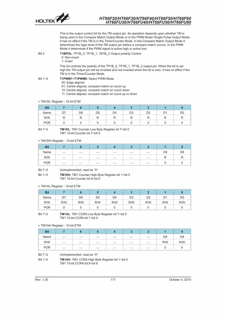
HT66F20/HT66F30/HT66F40/HT66F50/HT66F60HT66FU30/HT66FU40/HT66FU50/HT66FU60
Rev. 1.30 117 October 4, 2010
This is the output control bit for the TM output pin. Its operation depends upon whether TM is
being used in the Compare Match Output Mode or in the PWM Mode/ Single Pulse Output Mode.
It has no effect if the TM is in the Timer/Counter Mode. In the Compare Match Output Mode it
determines the logic level of the TM output pin before a compare match occurs. In the PWM
Mode it determines if the PWM signal is active high or active low.
Bit 2 T1BPOL: TP1B_0, TP1B_1, TB1B_2 Output polarity Control
0: Non-invert
1: Invert
This bit controls the polarity of the TP1B_0, TP1B_1, TP1B_2 output pin. When the bit is set
high the TM output pin will be inverted and not inverted when the bit is zero. It has no effect if the
TM is in the Timer/Counter Mode.
Bit 1~0 T1PWM1~T1PWM0: Select PWM Mode
00: Edge aligned
01: Centre aligned, compare match on count up
10: Centre aligned, compare match on count down
11: Centre aligned, compare match on count up or down
� TM1DL Register - 10-bit ETM
Bit 7 6 5 4 3 2 1 0
Name D7 D6 D5 D4 D3 D2 D1 D0
R/W R R R R R R R R
POR 0 0 0 0 0 0 0 0
Bit 7~0 TM1DL: TM1 Counter Low Byte Register bit 7~bit 0
TM1 10-bit Counter bit 7~bit 0
� TM1DH Register - 10-bit ETM
Bit 7 6 5 4 3 2 1 0
Name � � � � � � D9 D8
R/W � � � � � � R R
POR � � � � � � 0 0
Bit 7~2 Unimplemented, read as �0�
Bit 1~0 TM1DH: TM1 Counter High Byte Register bit 1~bit 0
TM1 10-bit Counter bit 9~bit 8
� TM1AL Register - 10-bit ETM
Bit 7 6 5 4 3 2 1 0
Name D7 D6 D5 D4 D3 D2 D1 D0
R/W R/W R/W R/W R/W R/W R/W R/W R/W
POR 0 0 0 0 0 0 0 0
Bit 7~0 TM1AL: TM1 CCRA Low Byte Register bit 7~bit 0
TM1 10-bit CCRA bit 7~bit 0
� TM1AH Register - 10-bit ETM
Bit 7 6 5 4 3 2 1 0
Name � � � � � � D9 D8
R/W � � � � � � R/W R/W
POR � � � � � � 0 0
Bit 7~2 Unimplemented, read as �0�
Bit 1~0 TM1AH: TM1 CCRA High Byte Register bit 1~bit 0
TM1 10-bit CCRA bit 9~bit 8
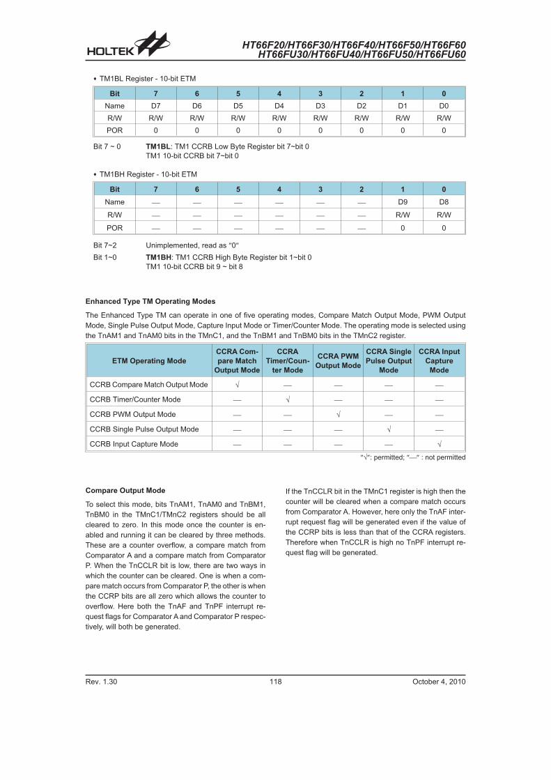
HT66F20/HT66F30/HT66F40/HT66F50/HT66F60HT66FU30/HT66FU40/HT66FU50/HT66FU60
Rev. 1.30 118 October 4, 2010
� TM1BL Register - 10-bit ETM
Bit 7 6 5 4 3 2 1 0
Name D7 D6 D5 D4 D3 D2 D1 D0
R/W R/W R/W R/W R/W R/W R/W R/W R/W
POR 0 0 0 0 0 0 0 0
Bit 7 ~ 0 TM1BL: TM1 CCRB Low Byte Register bit 7~bit 0
TM1 10-bit CCRB bit 7~bit 0
� TM1BH Register - 10-bit ETM
Bit 7 6 5 4 3 2 1 0
Name � � � � � � D9 D8
R/W � � � � � � R/W R/W
POR � � � � � � 0 0
Bit 7~2 Unimplemented, read as �0�
Bit 1~0 TM1BH: TM1 CCRB High Byte Register bit 1~bit 0
TM1 10-bit CCRB bit 9 ~ bit 8
Enhanced Type TM Operating Modes
The Enhanced Type TM can operate in one of five operating modes, Compare Match Output Mode, PWM Output
Mode, Single Pulse Output Mode, Capture Input Mode or Timer/Counter Mode. The operating mode is selected using
the TnAM1 and TnAM0 bits in the TMnC1, and the TnBM1 and TnBM0 bits in the TMnC2 register.
ETM Operating Mode
CCRA Com-
pare Match
Output Mode
CCRA
Timer/Coun-
ter Mode
CCRA PWM
Output Mode
CCRA Single
Pulse Output
Mode
CCRA Input
Capture
Mode
CCRB Compare Match Output Mode � � � � �
CCRB Timer/Counter Mode � � � � �
CCRB PWM Output Mode � � � � �
CCRB Single Pulse Output Mode � � � � �
CCRB Input Capture Mode � � � � �
���: permitted; ��� : not permitted
Compare Output Mode
To select this mode, bits TnAM1, TnAM0 and TnBM1,
TnBM0 in the TMnC1/TMnC2 registers should be all
cleared to zero. In this mode once the counter is en-
abled and running it can be cleared by three methods.
These are a counter overflow, a compare match from
Comparator A and a compare match from Comparator
P. When the TnCCLR bit is low, there are two ways in
which the counter can be cleared. One is when a com-
pare match occurs from Comparator P, the other is when
the CCRP bits are all zero which allows the counter to
overflow. Here both the TnAF and TnPF interrupt re-
quest flags for Comparator A and Comparator P respec-
tively, will both be generated.
If the TnCCLR bit in the TMnC1 register is high then the
counter will be cleared when a compare match occurs
from Comparator A. However, here only the TnAF inter-
rupt request flag will be generated even if the value of
the CCRP bits is less than that of the CCRA registers.
Therefore when TnCCLR is high no TnPF interrupt re-
quest flag will be generated.

HT66F20/HT66F30/HT66F40/HT66F50/HT66F60HT66FU30/HT66FU40/HT66FU50/HT66FU60
Rev. 1.30 119 October 4, 2010
As the name of the mode suggests, after a comparison
is made, the TM output pin, will change state. The TM
output pin condition however only changes state when
an TnAF or TnBF interrupt request flag is generated af-
ter a compare match occurs from Comparator A or Com-
parator B. The TnPF interrupt request flag, generated
from a compare match from Comparator P, will have no
effect on the TM output pin. The way in which the TM
output pin changes state is determined by the condition
of the TnAIO1 and TnAIO0 bits in the TMnC1 register for
ETM CCRA, and the TnBIO1 and TnBIO0 bits in the
TMnC2 register for ETM CCRB. The TM output pin can
be selected using the TnAIO1, TnAIO0 bits (for the
TPnA pin) and TnBIO1, TnBIO0 bits (for the TPnB_0,
TPnB_1 or TPnB_2 pins) to go high, to go low or to tog-
gle from its present condition when a compare match
occurs from Comparator A or a compare match occurs
from Comparator B. The initial condition of the TM out-
put pin, which is setup after the TnON bit changes from
low to high, is setup using the TnAOC or TnBOC bit for
TPnA or TPnB_0, TPnB_1, TPnB_2 output pins. Note
that if the TnAIO1,TnAIO0 and TnBIO1, TnBIO0 bits are
zero then no pin change will take place.
Counter Value
0x3FF
CCRP
CCRA
TnON
TnPAU
TnAPOL
CCRP Int.
Flag TnPF
CCRA Int.
Flag TnAF
TPnA O/P
Pin
Time
CCRP=0
CCRP > 0
Counter overflow
CCRP > 0Counter cleared by CCRP value
Pause
Resume
Stop
CounterRestart
TnCCLR = 0; TnAM [1:0] = 00
Output pin set to
initial Level Low
if TnAOC=0
Output Toggle with
TnAF flag
Note TnAIO [1:0] = 10
Active High Output selectHere TnAIO [1:0] = 11
Toggle Output select
Output not affected by TnAF
flag. Remains High until reset
by TnON bit
Output Pin
Reset to Initial value
Output controlled by
other pin-shared function
Output Inverts
when TnAPOL is high
ETM CCRA Compare Match Output Mode -- TnCCLR = 0
Note: 1. With TnCCLR=0 a Comparator P match will clear the counter
2. The TPnA output pin is controlled only by the TnAF flag
3. The output pin is reset to its initial state by a TnON bit rising edge

HT66F20/HT66F30/HT66F40/HT66F50/HT66F60HT66FU30/HT66FU40/HT66FU50/HT66FU60
Rev. 1.30 120 October 4, 2010
Counter Value
0x3FF
CCRP
CCRB
TnON
TnPAU
TnBPOL
CCRP Int.
Flag TnPF
CCRB Int.
Flag TnBF
TPnB O/P
Pin
Time
CCRP=0
CCRP > 0
Counter overflow
CCRP > 0Counter cleared by CCRP value
Pause
Resume
Stop
CounterRestart
TnCCLR = 0; TnBM [1:0] = 00
Output pin set to
initial Level Low
if TnBOC=0
Output Toggle with
TnBF flag
Note TnBIO [1:0] = 10
Active High Output selectHere TnBIO [1:0] = 11
Toggle Output select
Output not affected by TnBF
flag. Remains High until reset
by TnON bit
Output Pin
Reset to Initial value
Output controlled by
other pin-shared function
Output Inverts
when TnBPOL is high
ETM CCRB Compare Match Output Mode -- TnCCLR = 0
Note: 1. With TnCCLR=0 a Comparator P match will clear the counter
2. The TPnB output pin is controlled only by the TnBF flag
3. The output pin is reset to its initial state by a TnON bit rising edge

HT66F20/HT66F30/HT66F40/HT66F50/HT66F60HT66FU30/HT66FU40/HT66FU50/HT66FU60
Rev. 1.30 121 October 4, 2010
Counter Value
0x3FF
CCRP
CCRA
TnON
TnPAU
TnAPOL
CCRP Int.
Flag TnPF
CCRA Int.
Flag TnAF
TPnA O/P
Pin
Time
CCRA=0
CCRA = 0Counter overflow
CCRA > 0 Counter cleared by CCRA value
Pause
Resume
Stop Counter Restart
TnCCLR = 1; TnAM [1:0] = 00
Output pin set to
initial Level Low
if TnAOC=0
Output Toggle with
TnAF flag
Note TnAIO [1:0] = 10
Active High Output selectHere TnAIO [1:0] = 11
Toggle Output select
Output not affected by
TnAF flag. Remains High
until reset by TnON bitOutput Pin
Reset to Initial value
Output controlled by
other pin-shared function
Output Inverts
when TnAPOL is high
TnPF notgenerated
No TnAF flaggenerated onCCRA overflow
Output doesnot change
ETM CCRA Compare Match Output Mode -- TnCCLR = 1
Note: 1. With TnCCLR=1 a Comparator A match will clear the counter
2. The TPnA output pin is controlled only by the TnAF flag
3. The TPnA output pin is reset to its initial state by a TnON bit rising edge
4. The TnPF flag is not generated when TnCCLR=1

HT66F20/HT66F30/HT66F40/HT66F50/HT66F60HT66FU30/HT66FU40/HT66FU50/HT66FU60
Rev. 1.30 122 October 4, 2010
Counter Value
0x3FF
CCRB
CCRA
TnON
TnPAU
TnBPOL
CCRB Int.
Flag TnBF
CCRA Int.
Flag TnAF
TPnB O/P
Pin
Time
CCRA=0
CCRA = 0Counter overflow
CCRA > 0 Counter cleared by CCRA value
Pause
Resume
Stop Counter Restart
TnCCLR = 1; TnBM [1:0] = 00
Output pin set to
initial Level Low
if TnBOC=0
Output Toggle with
TnBF flag
Note TnBIO [1:0] = 10
Active High Output selectHere TnBIO [1:0] = 11
Toggle Output select
Output not affected by
TnBF flag. Remains High
until reset by TnON bitOutput Pin
Reset to Initial value
Output controlled by
other pin-shared function
Output Inverts
when TnBPOL is high
No TnAF flaggenerated onCCRA overflow
ETM CCRB Compare Match Output Mode -- TnCCLR = 1
Note: 1. With TnCCLR=1 a Comparator A match will clear the counter
2. The TPnB output pin is controlled only by the TnBF flag
3. The TPnB output pin is reset to its initial state by a TnON bit rising edge
4. The TnPF flag is not generated when TnCCLR=1

HT66F20/HT66F30/HT66F40/HT66F50/HT66F60HT66FU30/HT66FU40/HT66FU50/HT66FU60
Rev. 1.30 123 October 4, 2010
Timer/Counter Mode
To select this mode, bits TnAM1, TnAM0 and TnBM1,
TnBM0 in the TMnC1 and TMnC2 register should all be
set high. The Timer/Counter Mode operates in an identi-
cal way to the Compare Match Output Mode generating
the same interrupt flags. The exception is that in the
Timer/Counter Mode the TM output pin is not used.
Therefore the above description and Timing Diagrams
for the Compare Match Output Mode can be used to un-
derstand its function. As the TM output pin is not used in
this mode, the pin can be used as a normal I/O pin or
other pin-shared function.
PWM Output Mode
To select this mode, the required bit pairs, TnAM1,
TnAM0 and TnBM1, TnBM0 should be set to 10 respec-
tively and also the TnAIO1, TnAIO0 and TnBIO1,
TnBIO0 bits should be set to 10 respectively. The PWM
function within the TM is useful for applications which re-
quire functions such as motor control, heating control, il-
lumination control etc. By providing a signal of fixed
frequency but of varying duty cycle on the TM output pin,
a square wave AC waveform can be generated with
varying equivalent DC RMS values.
As both the period and duty cycle of the PWM waveform
can be controlled, the choice of generated waveform is
extremely flexible. In the PWM mode, the TnCCLR bit is
used to determine in which way the PWM period is con-
trolled. With the TnCCLR bit set high, the PWM period
can be finely controlled using the CCRA registers. In this
case the CCRB registers are used to set the PWM duty
value (for TPnB output pins). The CCRP bits are not used
and TPnA output pin is not used. The PWM output can
only be generated on the TPnB output pins. With the
TnCCLR bit cleared to zero, the PWM period is set using
one of the eight values of the three CCRP bits, in multi-
ples of 128. Now both CCRA and CCRB registers can be
used to setup different duty cycle values to provide dual
PWM outputs on their relative TPnA and TPnB pins.
The TnPWM1 and TnPWM0 bits determine the PWM
alignment type, which can be either edge or centre type.
In edge alignment, the leading edge of the PWM signals
will all be generated concurrently when the counter is re-
set to zero. With all power currents switching on at the
same time, this may give rise to problems in higher
power applications. In centre alignment the centre of the
PWM active signals will occur sequentially, thus reduc-
ing the level of simultaneous power switching currents.
Interrupt flags, one for each of the CCRA, CCRB and
CCRP, will be generated when a compare match occurs
from either the Comparator A, Comparator B or Com-
parator P. The TnAOC and TnBOC bits in the TMnC1 and
TMnC2 register are used to select the required polarity of
the PWM waveform while the two TnAIO1, TnAIO0 and
TnBIO1, TnBIO0 bits pairs are used to enable the PWM
output or to force the TM output pin to a fixed high or low
level. The TnAPOL and TnBPOL bit are used to reverse
the polarity of the PWM output waveform.
� ETM, PWM Mode, Edge-aligned Mode, TnCCLR=0
CCRP 001b 010b 011b 100b 101b 110b 111b 000b
Period 128 256 384 512 640 768 896 1024
A Duty CCRA
B Duty CCRB
If fSYS = 16MHz, TM clock source select fSYS/4, CCRP = 100b, CCRA = 128 and CCRB = 256,
The TP1A PWM output frequency = (fSYS/4) / 512 = fSYS/2048 = 7.8125kHz, duty = 128/512 = 25%.
The TP1B_n PWM output frequency = (fSYS/4) / 512 = fSYS/2048 = 7.8125kHz, duty = 256/512 = 50%.
If the Duty value defined by CCRA or CCRB register is equal to or greater than the Period value, then the PWM output
duty is 100%.
� ETM, PWM Mode, Edge-aligned Mode, TnCCLR=1
CCRA 1 2 3 511 512 1021 1022 1023
Period 1 2 3 511 512 1021 1022 1023
B Duty CCRB
� ETM, PWM Mode, Center-aligned Mode, TnCCLR=0
CCRP 001b 010b 011b 100b 101b 110b 111b 000b
Period 256 512 768 1024 1280 1536 1792 2046
A Duty (CCRA�2)1
B Duty (CCRB�2)1

HT66F20/HT66F30/HT66F40/HT66F50/HT66F60HT66FU30/HT66FU40/HT66FU50/HT66FU60
Rev. 1.30 124 October 4, 2010
Counter Value
CCRP
CCRA
TnON
TnPAU
TnAPOL
CCRA Int.
Flag TnAF
CCRB Int.
Flag TnBF
TPnA Pin(TnAOC=1)
Time
Counter Cleared by CCRP
PauseResume Stop
CounterRestart
TnCCLR = 0;
TnAM [1:0] = 10, TnBM [1:0] = 10;
TnPWM [1:0] = 00
Output Pin
Reset to Initial value
Output controlled by
other pin-shared function
Output Invertswhen TnAPOLis high
CCRB
CCRP Int.
Flag TnPF
TPnB Pin(TnBOC=1)
TPnB Pin(TnBOC=0)
Duty Cycle
set by CCRA
Duty Cycle
set by CCRB
PWM Period set by CCRP
Duty Cycle
set by CCRA
Duty Cycle
set by CCRA
ETM PWM Mode -- Edge Aligned
Note: 1. Here TnCCLR=0 therefore CCRP clears counter and determines the PWM period
2. The internal PWM function continues running even when TnAIO [1:0] (or TnBIO [1:0]) = 00 or 01
3. CCRA controls the TPnA PWM duty and CCRB controls the TPnB PWM duty
� ETM, PWM Mode, Center-aligned Mode, TnCCLR=1
CCRA 1 2 3 511 512 1021 1022 1023
Period 2 4 6 1022 1024 2042 2044 2046
B Duty (CCRB�2)1

HT66F20/HT66F30/HT66F40/HT66F50/HT66F60HT66FU30/HT66FU40/HT66FU50/HT66FU60
Rev. 1.30 125 October 4, 2010
Counter Value
CCRA
TnON
TnPAU
TnBPOL
CCRB Int.
Flag TnBF
Time
Counter Cleared by CCRA
PauseResume Stop
CounterRestart
TnCCLR = 1; TnBM [1:0] = 10;
TnPWM [1:0] = 00
Output Pin
Reset to
Initial valueOutput controlled by
other pin-shared function
Output Invertswhen TnBPOLis high
CCRB
CCRP Int.
Flag TnPF
TPnB Pin(TnBOC=1)
TPnB Pin(TnBOC=0)
Duty Cycle
set by CCRB
PWM Period set by CCRA
ETM PWM Mode -- Edge Aligned
Note: 1. Here TnCCLR=1 therefore CCRA clears the counter and determines the PWM period
2. The internal PWM function continues running even when TnBIO [1:0] = 00 or 01
3. The CCRA controls the TPnB PWM period and CCRB controls the TPnB PWM duty
4. Here the TM pin control register should not enable the TPnA pin as a TM output pin.

HT66F20/HT66F30/HT66F40/HT66F50/HT66F60HT66FU30/HT66FU40/HT66FU50/HT66FU60
Rev. 1.30 126 October 4, 2010
Counter Value
CCRP
CCRA
TnON
TnPAU
TnAPOL
CCRA Int.
Flag TnAF
CCRB Int.
Flag TnBF
TPnA Pin(TnAOC=1)
Time
Pause
ResumeStop
CounterRestart
TnCCLR = 0;
TnAM [1:0] = 10, TnBM [1:0] = 10;
TnPWM [1:0] = 11
Output Pin
Reset to Initial value
Output controlled by
Other pin-shared function
Output Invertswhen TnAPOLis high
CCRB
CCRP Int.
Flag TnPF
TPnB Pin(TnBOC=1)
TPnB Pin(TnBOC=0)
Duty Cycle set by CCRA
Duty Cycle set by CCRB
PWM Period set by CCRP
ETM PWM Mode -- Centre Aligned
Note: 1. Here TnCCLR=0 therefore CCRP clears the counter and determines the PWM period
2. TnPWM [1:0] =11 therefore the PWM is centre aligned
3. The internal PWM function continues running even when TnAIO [1:0] (or TnBIO [1:0]) = 00 or 01
4. CCRA controls the TPnA PWM duty and CCRB controls the TPnB PWM duty
5. CCRP will generate an interrupt request when the counter decrements to its zero value

HT66F20/HT66F30/HT66F40/HT66F50/HT66F60HT66FU30/HT66FU40/HT66FU50/HT66FU60
Rev. 1.30 127 October 4, 2010
Counter Value
CCRP
CCRA
TnON
TnPAU
TnAPOL
CCRA Int.
Flag TnAF
CCRB Int.
Flag TnBF
TPnA Pin(TnAOC=1)
Time
Pause
ResumeStop
CounterRestart
TnCCLR = 0;
TnAM [1:0] = 10, TnBM [1:0] = 10;
TnPWM [1:0] = 11
Output Pin
Reset to Initial value
Output controlled by
Other pin-shared function
Output Invertswhen TnAPOLis high
CCRB
CCRP Int.
Flag TnPF
TPnB Pin(TnBOC=1)
TPnB Pin(TnBOC=0)
Duty Cycle set by CCRA
Duty Cycle set by CCRB
PWM Period set by CCRP
ETM PWM Mode -- Centre Aligned
Note: 1. Here TnCCLR=1 therefore CCRA clears the counter and determines the PWM period
2. TnPWM [1:0] =11 therefore the PWM is centre aligned
3. The internal PWM function continues running even when TnBIO [1:0] = 00 or 01
4. CCRA controls the TPnB PWM period and CCRB controls the TPnB PWM duty
5. CCRP will generate an interrupt request when the counter decrements to its zero value

HT66F20/HT66F30/HT66F40/HT66F50/HT66F60HT66FU30/HT66FU40/HT66FU50/HT66FU60
Rev. 1.30 128 October 4, 2010
Single Pulse Output Mode
To select this mode, the required bit pairs, TnAM1,
TnAM0 and TnBM1, TnBM0 should be set to 10 respec-
tively and also the corresponding TnAIO1, TnAIO0 and
TnBIO1, TnBIO0 bits should be set to 11 respectively.
The Single Pulse Output Mode, as the name suggests,
will generate a single shot pulse on the TM output pin.
The trigger for the pulse TPnA output leading edge is a
low to high transition of the TnON bit, which can be im-
plemented using the application program. The trigger
for the pulse TPnB output leading edge is a compare
match from Comparator B, which can be implemented
using the application program. However in the Single
Pulse Mode, the TnON bit can also be made to automat-
ically change from low to high using the external TCKn
pin, which will in turn initiate the Single Pulse output of
TPnA. When the TnON bit transitions to a high level, the
counter will start running and the pulse leading edge of
TPnA will be generated. The TnON bit should remain
high when the pulse is in its active state. The generated
pulse trailing edge of TPnA and TPnB will be generated
when the TnON bit is cleared to zero, which can be im-
plemented using the application program or when a
compare match occurs from Comparator A.
However a compare match from Comparator A will also
automatically clear the TnON bit and thus generate the
Single Pulse output trailing edge of TPnA and TPnB. In
this way the CCRA value can be used to control the
pulse width of TPnA. The CCRA-CCRB value can be
used to control the pulse width of TPnB. A compare
match from Comparator A and Comparator B will also
generate TM interrupts. The counter can only be reset
back to zero when the TnON bit changes from low to
high when the counter restarts. In the Single Pulse
Mode CCRP is not used. The TnCCLR bit is also not
used.
Single Pulse Generation

HT66F20/HT66F30/HT66F40/HT66F50/HT66F60HT66FU30/HT66FU40/HT66FU50/HT66FU60
Rev. 1.30 129 October 4, 2010
Counter Value
CCRB
CCRA
TnON
TnPAU
TnAPOL
CCRB Int.
Flag TnBF
CCRA Int.
Flag TnAF
TPnA Pin(TnAOC=1)
Time
Counter stoppedby CCRA
PauseResume Counter Stops
by software
Counter Resetwhen TnONreturns high
TnAM [1:0] = 10, TnBM [1:0] = 10;
TnAIO [1:0] = 11, TnBIO [1:0] = 11
Pulse Width set
by (CCRA-CCRB) Output Inverts
when TnBPOL=1
TCKn pin
SoftwareTrigger
Cleared byCCRA match
TCKn pinTrigger
Auto. set byTCKn pin
SoftwareTrigger
SoftwareClear
SoftwareTriggerSoftware
Trigger
TnBPOL
TPnA Pin(TnAOC=0)
TPnB Pin(TnBOC=1)
TPnB Pin(TnBOC=0)
Pulse Width
set by CCRA
Output Inverts
when TnAPOL=1
ETM -- Single Pulse Mode
Note: 1. Counter stopped by CCRA
2. CCRP is not used
3. The pulse is triggered by the TCKn pin or by setting the TnON bit high
4. A TCKn pin active edge will automatically set the TnON bit high
5. In the Single Pulse Mode, TnAIO [1:0] and TnBIO [1:0] must be set to �11� and can not be changed.

HT66F20/HT66F30/HT66F40/HT66F50/HT66F60HT66FU30/HT66FU40/HT66FU50/HT66FU60
Rev. 1.30 130 October 4, 2010
Capture Input Mode
To select this mode bits TnAM1, TnAM0 and TnBM1,
TnBM0 in the TMnC1 and TMnC2 registers should be
set to 01 respectively. This mode enables external sig-
nals to capture and store the present value of the inter-
nal counter and can therefore be used for applications
such as pulse width measurements. The external signal
is supplied on the TPnA and TPnB_0, TPnB_1, TPnB_2
pins, whose active edge can be either a rising edge, a
falling edge or both rising and falling edges; the active
edge transition type is selected using the TnAIO1,
TnAIO0 and TnBIO1, TnBIO0 bits in the TMnC1 and
TMnC2 registers. The counter is started when the TnON
bit changes from low to high which is initiated using the
application program.
When the required edge transition appears on the TPnA
and TPnB_0, TPnB_1, TPnB_2 pins the present value
in the counter will be latched into the CCRA and CCRB
registers and a TM interrupt generated. Irrespective of
what events occur on the TPnA and TPnB_0, TPnB_1,
TPnB_2 pins the counter will continue to free run until
the TnON bit changes from high to low. When a CCRP
compare match occurs the counter will reset back to
zero; in this way the CCRP value can be used to control
the maximum counter value. When a CCRP compare
match occurs from Comparator P, a TM interrupt will
also be generated. Counting the number of overflow in-
terrupt signals from the CCRP can be a useful method in
measuring long pulse widths. The TnAIO1, TnAIO0 and
TnBIO1, TnBIO0 bits can select the active trigger edge
on the TPnA and TPnB_0, TPnB_1, TPnB_2 pins to be
a rising edge, falling edge or both edge types. If the
TnAIO1, TnAIO0 and TnBIO1, TnBIO0 bits are both set
high, then no capture operation will take place irrespec-
tive of what happens on the TPnA and TPnB_0,
TPnB_1, TPnB_2 pins, however it must be noted that
the counter will continue to run.
As the TPnA and TPnB_0, TPnB_1, TPnB_2 pins are
pin shared with other functions, care must be taken if the
TM is in the Capture Input Mode. This is because if the
pin is setup as an output, then any transitions on this pin
may cause an input capture operation to be executed.
The TnCCLR, TnAOC, TnBOC, TnAPOL and TnBPOL
bits are not used in this mode.
Counter Value
YY
CCRP
TnON
TnPAU
CCRP Int.
Flag TnPF
CCRA Int.
Flag TnAF
CCRAValue
Time
Counter clearedby CCRP
PauseResume
CounterReset
TnAM [1:0] = 01
TM capture
pin TPnA
XX
CounterStop
TnAIO [1:0]Value
XX YY XX YY
Activeedge
Activeedge
Active edge
00 Rising edge 01 Falling edge 10 Both edges 11 Disable Capture
ETM CCRA Capture Input Mode
Note: 1. TnAM [1:0] = 01 and active edge set by the TnAIO [1:0] bits
2. The TM Capture input pin active edge transfers he counter value to CCRA
3. TnCCLR bit not used
4. No output function -- TnAOC and TnAPOL bits not used
5. CCRP determines the counter value and the counter has a maximum count value when CCRP is equal
to zero.

HT66F20/HT66F30/HT66F40/HT66F50/HT66F60HT66FU30/HT66FU40/HT66FU50/HT66FU60
Rev. 1.30 131 October 4, 2010
CCRP
Counter
overflow
CCRP Int.
Flag TnPF
CCRB Int.
Flag TnBF
TnON bit
Pause
Counter
Reset
TnPAU bit
Resume
Stop
YY
XX
CCRB
Value XX
TM Capture Pin
YY
TnBIO1, TnBIO0
Value 00 - Rising edge 01 - Falling edge 11 - Disable Capture
Active
edge
Active
edge
XX
10 - Both edges
Active
edges
YY
TnBM1, TnBM0 = 01
Time
Counter
Value
ETM CCRB Capture Input Mode
Note: 1. TnBM [1:0] = 01 and active edge set by the TnBIO [1:0] bits
2. The TM Capture input pin active edge transfers the counter value to CCRB
3. TnCCLR bit not used
4. No output function -- TnBOC and TnBPOL bits not used
5. CCRP determines the counter value and the counter has a maximum count value when CCRP
is equal to zero.
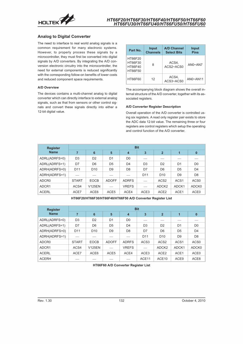
HT66F20/HT66F30/HT66F40/HT66F50/HT66F60HT66FU30/HT66FU40/HT66FU50/HT66FU60
Rev. 1.30 132 October 4, 2010
Analog to Digital Converter
The need to interface to real world analog signals is a
common requirement for many electronic systems.
However, to properly process these signals by a
microcontroller, they must first be converted into digital
signals by A/D converters. By integrating the A/D con-
version electronic circuitry into the microcontroller, the
need for external components is reduced significantly
with the corresponding follow-on benefits of lower costs
and reduced component space requirements.
A/D Overview
The devices contains a multi-channel analog to digital
converter which can directly interface to external analog
signals, such as that from sensors or other control sig-
nals and convert these signals directly into either a
12-bit digital value.
Part No.Input
Channels
A/D Channel
Select Bits
Input
Pins
HT66F20
HT66F30
HT66F40
HT66F50
8ACS4,
ACS2~ACS0AN0~AN7
HT66F60 12ACS4,
ACS3~ACS0AN0~AN11
The accompanying block diagram shows the overall in-
ternal structure of the A/D converter, together with its as-
sociated registers.
A/D Converter Register Description
Overall operation of the A/D converter is controlled us-
ing six registers. A read only register pair exists to store
the ADC data 12-bit value. The remaining three or four
registers are control registers which setup the operating
and control function of the A/D converter.
Register
Name
Bit
7 6 5 4 3 2 1 0
ADRL(ADRFS=0) D3 D2 D1 D0 � � � �
ADRL(ADRFS=1) D7 D6 D5 D4 D3 D2 D1 D0
ADRH(ADRFS=0) D11 D10 D9 D8 D7 D6 D5 D4
ADRH(ADRFS=1) � � � � D11 D10 D9 D8
ADCR0 START EOCB ADOFF ADRFS � ACS2 ACS1 ACS0
ADCR1 ACS4 V125EN � VREFS � ADCK2 ADCK1 ADCK0
ACERL ACE7 ACE6 ACE5 ACE4 ACE3 ACE2 ACE1 ACE0
HT66F20/HT66F30/HT66F40/HT66F50 A/D Converter Register List
Register
Name
Bit
7 6 5 4 3 2 1 0
ADRL(ADRFS=0) D3 D2 D1 D0 � � � �
ADRL(ADRFS=1) D7 D6 D5 D4 D3 D2 D1 D0
ADRH(ADRFS=0) D11 D10 D9 D8 D7 D6 D5 D4
ADRH(ADRFS=1) � � � � D11 D10 D9 D8
ADCR0 START EOCB ADOFF ADRFS ACS3 ACS2 ACS1 ACS0
ADCR1 ACS4 V125EN � VREFS � ADCK2 ADCK1 ADCK0
ACERL ACE7 ACE6 ACE5 ACE4 ACE3 ACE2 ACE1 ACE0
ACERH � � � � ACE11 ACE10 ACE9 ACE8
HT66F60 A/D Converter Register List

HT66F20/HT66F30/HT66F40/HT66F50/HT66F60HT66FU30/HT66FU40/HT66FU50/HT66FU60
Rev. 1.30 133 October 4, 2010
A/D Converter Data Registers � ADRL, ADRH
As the devices contain an internal 12-bit A/D converter, they require two data registers to store the converted value.
These are a high byte register, known as ADRH, and a low byte register, known as ADRL. After the conversion process
takes place, these registers can be directly read by the microcontroller to obtain the digitised conversion value. As only
12 bits of the 16-bit register space is utilised, the format in which the data is stored is controlled by the ADRFS bit in the
ADCR0 register as shown in the accompanying table. D0~D11 are the A/D conversion result data bits. Any unused bits
will be read as zero.
ADRFSADRH ADRL
7 6 5 4 3 2 1 0 7 6 5 4 3 2 1 0
0 D11 D10 D9 D8 D7 D6 D5 D4 D3 D2 D1 D0 0 0 0 0
1 0 0 0 0 D11 D10 D9 D8 D7 D6 D5 D4 D3 D2 D1 D0
A/D Data Registers
� � � � � � � � � �
� � � � � � � � � � � � � � � � � � � � � � � � � � � � � � � � � � � � � � �
� � � � � � � � � � � � � � � �
� � � �
� � �
� � � � � � � �� � ! " � � "
� � # $ � � % & � � & � ' � ( � � ' � �
� % %
( $ � � � � �� � � ) # � � � � ) �
� % * %
� � � � � � � � � �
� � % + � � � % �
� , # $ �
� � � � � � � � -
� � �
� � ' � �( ! � � � � � %
( ! �
� � � � %. ! �
� � � # �/ � 0 � � � 1
A/D Converter Structure
A/D Converter Control Registers �
ADCR0, ADCR1, ACERL, ACERH
To control the function and operation of the A/D con-
verter, three or four control registers known as ADCR0,
ADCR1, ACERL and ACERH are provided. These 8-bit
registers define functions such as the selection of which
analog channel is connected to the internal A/D con-
verter, the digitised data format, the A/D clock source as
well as controlling the start function and monitoring the
A/D converter end of conversion status. The
ACS3~ACS0 bits in the ADCR0 register and ACS4 bit is
the ADCR1 register define the ADC input channel num-
ber. As the device contains only one actual analog to
digital converter hardware circuit, each of the individual
8 or 12 analog inputs must be routed to the converter. It
is the function of the ACS4~ACS0 bits to determine
which analog channel input pins or internal 1.25V is ac-
tually connected to the internal A/D converter.
The ACERH and ACERL control registers contain the
ACER11~ACER0 bits which determine which pins on
Port A, PE6, PE7, PF0 and PF1 are used as analog in-
puts for the A/D converter input and which pins are not
to be used as the A/D converter input. Setting the corre-
sponding bit high will select the A/D input function, clear-
ing the bit to zero will select either the I/O or other
pin-shared function. When the pin is selected to be an
A/D input, its original function whether it is an I/O or
other pin-shared function will be removed. In addition,
any internal pull-high resistors connected to these pins
will be automatically removed if the pin is selected to be
an A/D input.

HT66F20/HT66F30/HT66F40/HT66F50/HT66F60HT66FU30/HT66FU40/HT66FU50/HT66FU60
Rev. 1.30 134 October 4, 2010
� ADCR0 Register
� HT66F20/HT66F30/HT66F40/HT66F50
Bit 7 6 5 4 3 2 1 0
Name START EOCB ADOFF ADRFS � ACS2 ACS1 ACS0
R/W R/W R R/W R/W � R/W R/W R/W
POR 0 1 1 0 � 0 0 0
Bit 7 START: Start the A/D conversion
0�1�0 : start
0�1 : reset the A/D converter and set EOCB to �1�
This bit is used to initiate an A/D conversion process. The bit is normally low but if set high and
then cleared low again, the A/D converter will initiate a conversion process. When the bit is set
high the A/D converter will be reset.
Bit 6 EOCB: End of A/D conversion flag
0: A/D conversion ended
1: A/D conversion in progress
This read only flag is used to indicate when an A/D conversion process has completed. When
the conversion process is running the bit will be high.
Bit 5 ADOFF : ADC module power on/off control bit
0: ADC module power on
1: ADC module power off
This bit controls the power to the A/D internal function. This bit should be cleared to zero to
enable the A/D converter. If the bit is set high then the A/D converter will be switched off reducing
the device power consumption. As the A/D converter will consume a limited amount of power,
even when not executing a conversion, this may be an important consideration in power sensitive
battery powered applications.
Note: 1. it is recommended to set ADOFF=1 before entering IDLE/SLEEP Mode for saving
power.
2. ADOFF=1 will power down the ADC module.
Bit 4 ADRFS: ADC Data Format Control
0: ADC Data MSB is ADRH bit 7, LSB is ADRL bit 4
1: ADC Data MSB is ADRH bit 3, LSB is ADRL bit 0
This bit controls the format of the 12-bit converted A/D value in the two A/D data registers.
Details are provided in the A/D data register section.
Bit 3 unimplemented, read as �0�
Bit 2~0 ACS2, ACS1, ACS0: Select A/D channel (when ACS4 is �0�)
000: AN0
001: AN1
010: AN2
011: AN3
100: AN4
101: AN5
110: AN6
111: AN7
These are the A/D channel select control bits. As there is only one internal hardware A/D
converter each of the eight A/D inputs must be routed to the internal converter using these bits.
If bit ACS4 in the ADCR1 register is set high then the internal 1.25V will be routed to the A/D
Converter.

HT66F20/HT66F30/HT66F40/HT66F50/HT66F60HT66FU30/HT66FU40/HT66FU50/HT66FU60
Rev. 1.30 135 October 4, 2010
� ADCR0 Register
� HT66F60
Bit 7 6 5 4 3 2 1 0
Name START EOCB ADOFF ADRFS ACS3 ACS2 ACS1 ACS0
R/W R/W R R/W R/W R/W R/W R/W R/W
POR 0 1 1 0 0 0 0 0
Bit 7 START: Start the A/D conversion
0�1�0 : start
0�1 : reset the A/D converter and set EOCB to �1�
This bit is used to initiate an A/D conversion process. The bit is normally low but if set high and
then cleared low again, the A/D converter will initiate a conversion process. When the bit is set
high the A/D converter will be reset.
Bit 6 EOCB: End of A/D conversion flag
0: A/D conversion ended
1: A/D conversion in progress
This read only flag is used to indicate when an A/D conversion process has completed. When
the conversion process is running the bit will be high.
Bit 5 ADOFF : ADC module power on/off control bit
0: ADC module power on
1: ADC module power off
This bit controls the power to the A/D internal function. This bit should be cleared to zero to
enable the A/D converter. If the bit is set high then the A/D converter will be switched off reducing
the device power consumption. As the A/D converter will consume a limited amount of power,
even when not executing a conversion, this may be an important consideration in power sensitive
battery powered applications.
Note: 1. it is recommended to set ADOFF=1 before entering IDLE/SLEEP Mode for saving
power.
2. ADOFF=1 will power down the ADC module.
Bit 4 ADRFS: ADC Data Format Control
0: ADC Data MSB is ADRH bit 7, LSB is ADRL bit 4
1: ADC Data MSB is ADRH bit 3, LSB is ADRL bit 0
This bit controls the format of the 12-bit converted A/D value in the two A/D data registers.
Details are provided in the A/D data register section.
Bit 3~0 ACS3, ACS2, ACS1, ACS0: Select A/D channel (when ACS4 is �0�)
0000: AN0
0001: AN1
0010: AN2
0011: AN3
0100: AN4
0101: AN5
0110: AN6
0111: AN7
1000: AN8
1001: AN9
1010: AN10
1011: AN11
1100~1111: undefined, can�t be used
These are the A/D channel select control bits. As there is only one internal hardware A/D
converter each of the eight A/D inputs must be routed to the internal converter using these bits.
If bit ACS4 in the ADCR1 register is set high then the internal 1.25V will be routed to the A/D
Converter.

HT66F20/HT66F30/HT66F40/HT66F50/HT66F60HT66FU30/HT66FU40/HT66FU50/HT66FU60
Rev. 1.30 136 October 4, 2010
� ADCR1 Register
Bit 7 6 5 4 3 2 1 0
Name ACS4 V125EN � VREFS � ADCK2 ADCK1 ADCK0
R/W R/W R/W � R/W � R/W R/W R/W
POR 0 0 � 0 � 0 0 0
Bit 7 ACS4: Selecte Internal 1.25V as ADC input Control
0: Disable
1: Enable
This bit enables 1.25V to be connected to the A/D converter. The V125EN bit must first have
been set to enable the bandgap circuit 1.25V voltage to be used by the A/D converter. When the
ACS4 bit is set high, the bandgap 1.25V voltage will be routed to the A/D converter and the other
A/D input channels disconnected.
Bit 6 V125EN: Internal 1.25V Control
0: Disable
1: Enable
This bit controls the internal Bandgap circuit on/off function to the A/D converter. When the bit
is set high the bandgap voltage 1.25V can be used by the A/D converter. If 1.25V is not used by
the A/D converter and the LVR/LVD function is disabled then the bandgap reference circuit will be
automatically switched off to conserve power. When 1.25V is switched on for use by the A/D
converter, a time tBG should be allowed for the bandgap circuit to stabilise before implementing
an A/D conversion.
Bit 5 unimplemented, read as �0�
Bit 4 VREFS: Selecte ADC reference voltage
0: Internal ADC power
1: VREF pin
This bit is used to select the reference voltage for the A/D converter. If the bit is high, then the
A/D converter reference voltage is supplied on the external VREF pin. If the pin is low, then the
internal reference is used which is taken from the power supply pin VDD.
Bit 3 unimplemented, read as �0�
Bit 2~0 ADCK2, ADCK1, ADCK0: Select ADC clock source
000: fSYS
001: fSYS/2
010: fSYS/4
011: fSYS/8
100: fSYS/16
101: fSYS/32
110: fSYS/64
111: Undefined
These three bits are used to select the clock source for the A/D converter.

HT66F20/HT66F30/HT66F40/HT66F50/HT66F60HT66FU30/HT66FU40/HT66FU50/HT66FU60
Rev. 1.30 137 October 4, 2010
� ACERL Register
Bit 7 6 5 4 3 2 1 0
Name ACE7 ACE6 ACE5 ACE4 ACE3 ACE2 ACE1 ACE0
R/W R/W R/W R/W R/W R/W R/W R/W R/W
POR 1 1 1 1 1 1 1 1
Bit 7 ACE7: Define PA7 is A/D input or not
0: Not A/D input
1: A/D input, AN7
Bit 6 ACE6: Define PA6 is A/D input or not
0: Not A/D input
1: A/D input, AN6
Bit 5 ACE5: Define PA5 is A/D input or not
0: Not A/D input
1: A/D input, AN5
Bit 4 ACE4: Define PA4 is A/D input or not
0: Not A/D input
1: A/D input, AN4
Bit 3 ACE3: Define PA3 is A/D input or not
0: Not A/D input
1: A/D input, AN3
Bit 2 ACE2: Define PA2 is A/D input or not
0: Not A/D input
1: A/D input, AN2
Bit 1 ACE1: Define PA1 is A/D input or not
0: Not A/D input
1: A/D input, AN1
Bit 0 ACE0: Define PA0 is A/D input or not
0: Not A/D input
1: A/D input, AN0
� ACERH Register
� HT66F60
Bit 7 6 5 4 3 2 1 0
Name � � � � ACE11 ACE10 ACE9 ACE8
R/W � � � � R/W R/W R/W R/W
POR � � � � 1 1 1 1
Bit 7~4 unimplemented, read as �0�
Bit 3 ACE11: Define PF1 is A/D input or not
0: Not A/D input
1: A/D input, AN11
Bit 2 ACE10: Define PF0 is A/D input or not
0: Not A/D input
1: A/D input, AN10
Bit 1 ACE9: Define PE7 is A/D input or not
0: Not A/D input
1: A/D input, AN9
Bit 0 ACE8: Define PE6 is A/D input or not
0: Not A/D input
1: A/D input, AN8

HT66F20/HT66F30/HT66F40/HT66F50/HT66F60HT66FU30/HT66FU40/HT66FU50/HT66FU60
Rev. 1.30 138 October 4, 2010
A/D Operation
The START bit in the ADCR0 register is used to start
and reset the A/D converter. When the microcontroller
sets this bit from low to high and then low again, an ana-
log to digital conversion cycle will be initiated. When the
START bit is brought from low to high but not low again,
the EOCB bit in the ADCR0 register will be set high and
the analog to digital converter will be reset. It is the
START bit that is used to control the overall start opera-
tion of the internal analog to digital converter.
The EOCB bit in the ADCR0 register is used to indicate
when the analog to digital conversion process is com-
plete. This bit will be automatically set to �0� by the
microcontroller after a conversion cycle has ended. In
addition, the corresponding A/D interrupt request flag
will be set in the interrupt control register, and if the inter-
rupts are enabled, an appropriate internal interrupt sig-
nal will be generated. This A/D internal interrupt signal
will direct the program flow to the associated A/D inter-
nal interrupt address for processing. If the A/D internal
interrupt is disabled, the microcontroller can be used to
poll the EOCB bit in the ADCR0 register to check
whether it has been cleared as an alternative method of
detecting the end of an A/D conversion cycle.
The clock source for the A/D converter, which originates
from the system clock fSYS, can be chosen to be either
fSYS or a subdivided version of fSYS. The division ratio
value is determined by the ADCK2~ADCK0 bits in the
ADCR1 register.
Although the A/D clock source is determined by the sys-
tem clock fSYS, and by bits ADCK2~ADCK0, there are
some limitations on the maximum A/D clock source
speed that can be selected. As the minimum value of per-
missible A/D clock period, tADCK, is 0.5�s, care must be
taken for system clock frequencies equal to or greater
than 4MHz. For example, if the system clock operates at
a frequency of 4MHz, the ADCK2~ADCK0 bits should
not be set to �000�. Doing so will give A/D clock periods
that are less than the minimum A/D clock period which
may result in inaccurate A/D conversion values. Refer to
the following table for examples, where values marked
with an asterisk * show where, depending upon the de-
vice, special care must be taken, as the values may be
less than the specified minimum A/D Clock Period.
fSYS
A/D Clock Period (tADCK)
ADCK2,
ADCK1,
ADCK0
= 000
(fSYS)
ADCK2,
ADCK1,
ADCK0
= 001
(fSYS/2)
ADCK2,
ADCK1,
ADCK0
= 010
(fSYS/4)
ADCK2,
ADCK1,
ADCK0
= 011
(fSYS/8)
ADCK2,
ADCK1,
ADCK0
= 100
(fSYS/16)
ADCK2,
ADCK1,
ADCK0
= 101
(fSYS/32)
ADCK2,
ADCK1,
ADCK0
= 110
(fSYS/64)
ADCK2,
ADCK1,
ADCK0
= 111
1MHz 1�s 2�s 4�s 8�s 16�s 32�s 64�s Undefined
2MHz 500ns 1�s 2�s 4�s 8�s 16�s 32�s Undefined
4MHz 250ns* 500ns 1�s 2�s 4�s 8�s 16�s Undefined
8MHz 125ns* 250ns* 500ns 1�s 2�s 4�s 8�s Undefined
12MHz 83ns* 167ns* 333ns* 667ns 1.33�s 2.67�s 5.33�s Undefined
A/D Clock Period Examples
Controlling the power on/off function of the A/D con-
verter circuitry is implemented using the ADOFF bit in
the ADCR0 register. This bit must be zero to power on
the A/D converter. When the ADOFF bit is cleared to
zero to power on the A/D converter internal circuitry a
certain delay, as indicated in the timing diagram, must
be allowed before an A/D conversion is initiated. Even if
no pins are selected for use as A/D inputs by clearing
the ACE11~ACE0 bits in the ACERH and ACERL regis-
ters, if the ADOFF bit is zero then some power will still
be consumed. In power conscious applications it is
therefore recommended that the ADOFF is set high to
reduce power consumption when the A/D converter
function is not being used.
The reference voltage supply to the A/D Converter can
be supplied from either the positive power supply pin,
VDD, or from an external reference sources supplied on
pin VREF. The desired selection is made using the
VREFS bit. As the VREF pin is pin-shared with other
functions, when the VREFS bit is set high, the VREF pin
function will be selected and the other pin functions will
be disabled automatically.
A/D Input Pins
All of the A/D analog input pins are pin-shared with the
I/O pins on Port A, PE6, PF7, PF0 or PF1 as well as
other functions. The ACE11~ ACE0 bits in the ACERH
and ACERL registers, determine whether the input pins
are setup as A/D converter analog inputs or whether
they have other functions. If the ACE11~ ACE0 bits for
its corresponding pin is set high then the pin will be
setup to be an A/D converter input and the original pin
functions disabled. In this way, pins can be changed un-
der program control to change their function between
A/D inputs and other functions. All pull-high resistors,
which are setup through register programming, will be
automatically disconnected if the pins are setup as A/D
inputs. Note that it is not necessary to first setup the A/D

HT66F20/HT66F30/HT66F40/HT66F50/HT66F60HT66FU30/HT66FU40/HT66FU50/HT66FU60
Rev. 1.30 139 October 4, 2010
pin as an input in the PAC, PEC or PFC port control reg-
ister to enable the A/D input as when the ACE11~ ACE0
bits enable an A/D input, the status of the port control
register will be overridden.
The A/D converter has its own reference voltage pin,
VREF, however the reference voltage can also be sup-
plied from the power supply pin, a choice which is made
through the VREFS bit in the ADCR1 register. The ana-
log input values must not be allowed to exceed the value
of VREF.
Summary of A/D Conversion Steps
The following summarises the individual steps that
should be executed in order to implement an A/D con-
version process.
� Step 1
Select the required A/D conversion clock by correctly
programming bits ADCK2~ADCK0 in the ADCR1 reg-
ister.
� Step 2
Enable the A/D by clearing the ADOFF bit in the
ADCR0 register to zero.
� Step 3
Select which channel is to be connected to the internal
A/D converter by correctly programming the
ACS4~ACS0 bits which are also contained in the
ADCR1 and ADCR0 register.
� Step 4
Select which pins are to be used as A/D inputs and
configure them by correctly programming the
ACE11~ACE0 bits in the ACERH and ACERL
registers.
� Step 5
If the interrupts are to be used, the interrupt control
registers must be correctly configured to ensure the
A/D converter interrupt function is active. The master
interrupt control bit, EMI, and the A/D converter inter-
rupt bit, EADI, must both be set high to do this.
� Step 6
The analog to digital conversion process can now be
initialised by setting the START bit in the ADCR regis-
ter from low to high and then low again. Note that this
bit should have been originally cleared to zero.
� Step 7
To check when the analog to digital conversion pro-
cess is complete, the EOCB bit in the ADCR0 register
can be polled. The conversion process is complete
when this bit goes low. When this occurs the A/D data
registers ADRL and ADRH can be read to obtain the
conversion value. As an alternative method, if the in-
terrupts are enabled and the stack is not full, the pro-
gram can wait for an A/D interrupt to occur.
Note: When checking for the end of the conversion
process, if the method of polling the EOCB bit in the
ADCR0 register is used, the interrupt enable step
above can be omitted.
� � � �
� � � � � � � � " ! � � � � ! 2
� � � � � ( � � � � � (
% & � � &
� ' � (
� � % + � � � % �
� 3 � 4 � �� " �
� � 5 � � � � � � �� � � � " ! � �� 6 � � � ! � � 7 � � � � � � � � ! � 8 � � � ! � �
# 6 � % � � � � � � � � � � � � 9 � � � �
% � � � � � � � � � � �� � � � " ! � �
� " � � � � �� � � � � �
� � � � " � 2 7 � ! � � � � ! 2 � � � � � % �
� � � � � (
% � � � � � � � � � � �� � � � " ! � �
� " � � � � �� � � � � �
� � � � � (
% � � � � � � � � � � �� � � � " ! � �
� " � � � � �� � � � � �
� � 5 � � � � � � �� � � � " ! � �
� � � � " � 2 7 � ! � � � � ! 2 � � � � � % �
� � � � �� �
� ' � # % &
� � � �
� � � � � � � � " ! � � � � ! 2
� � �
� � ' � �
� � � � : � 5 8 � ' �
A/D Conversion Timing
� � � � � � � � � � � � �
� , # $ �
� � # $ � �( 8 � � �
( $ � � � � �
� � �
� � � � %
� � � �
� # 4 . ! � � � � �( � � 5 � � 7� � � � � � � � � � �
; � 7 8 � � � � � � � �
� � % + � � � % �
A/D Input Structure

HT66F20/HT66F30/HT66F40/HT66F50/HT66F60HT66FU30/HT66FU40/HT66FU50/HT66FU60
Rev. 1.30 140 October 4, 2010
The accompanying diagram shows graphically the vari-
ous stages involved in an analog to digital conversion
process and its associated timing. After an A/D conver-
sion process has been initiated by the application pro-
gram, the microcontroller internal hardware will begin to
carry out the conversion, during which time the program
can continue with other functions. The time taken for the
A/D conversion is 16tADCK where tADCK is equal to the A/D
clock period.
Programming Considerations
During microcontroller operations where the A/D con-
verter is not being used, the A/D internal circuitry can be
switched off to reduce power consumption, by setting bit
ADOFF high in the ADCR0 register. When this happens,
the internal A/D converter circuits will not consume
power irrespective of what analog voltage is applied to
their input lines. If the A/D converter input lines are used
as normal I/Os, then care must be taken as if the input
voltage is not at a valid logic level, then this may lead to
some increase in power consumption.
A/D Transfer Function
As the devices contain a 12-bit A/D converter, its
full-scale converted digitised value is equal to FFFH.
Since the full-scale analog input value is equal to the
VDD or VREF voltage, this gives a single bit analog input
value of VDD or VREF divided by 4096.
1 LSB= (VDD or VREF) 4096
The A/D Converter input voltage value can be
calculated using the following equation:
A/D input voltage =
A/D output digital value (VDD or VREF) 4096
The diagram shows the ideal transfer function between
the analog input value and the digitised output value for
the A/D converter. Except for the digitised zero value,
the subsequent digitised values will change at a point
0.5 LSB below where they would change without the off-
set, and the last full scale digitised value will change at a
point 1.5 LSB below the VDD or VREF level.
A/D Programming Example
The following two programming examples illustrate how
to setup and implement an A/D conversion. In the first
example, the method of polling the EOCB bit in the
ADCR0 register is used to detect when the conversion
cycle is complete, whereas in the second example, the
A/D interrupt is used to determine when the conversion
is complete.
� � �
/ � � � � � � � � � � � � � � � � � � � � 1
� � � � � � � � " ! � �� " 8 � �
� � �
� � �
� <
� #
� �
� , $ � � % (
� � # < + � � < + � � + + � � $ + � � �
� � � � � � � ; � 7 8 � � � � � � � �
� , $ � � % (
� � � � � � � � � � �
+ � � �
Ideal A/D Transfer Function

HT66F20/HT66F30/HT66F40/HT66F50/HT66F60HT66FU30/HT66FU40/HT66FU50/HT66FU60
Rev. 1.30 141 October 4, 2010
Example: using an EOCB polling method to detect the end of conversion
clr EADI ; disable ADC interruptmov a,03Hmov ADCR1,a ; select fSYS/8 as A/D clock and switch off 1.25Vclr ADOFFmov a,0Fh ; setup ACERL and ACERH to configure pins AN0~AN3mov ACERL,amov a,00hmov ACERH,00h ; ACERH is only for HT66F60mov a,00hmov ADCR0,a ; enable and connect AN0 channel to A/D converter:
start_conversion:clr START ; high pulse on start bit to initiate conversionset START ; reset A/Dclr START ; start A/D
polling_EOC:sz EOCB ; poll the ADCR0 register EOCB bit to detect end
; of A/D conversionjmp polling_EOC ; continue pollingmov a,ADRL ; read low byte conversion result valuemov ADRL_buffer,a ; save result to user defined registermov a,ADRH ; read high byte conversion result valuemov ADRH_buffer,a ; save result to user defined register::jmp start_conversion ; start next a/d conversion
Example: using the interrupt method to detect the end of conversion
clr EADI ; disable ADC interruptmov a,03Hmov ADCR1,a ; select fSYS/8 as A/D clock and switch off 1.25VClr ADOFFmov a,0Fh ; setup ACERL and ACERH to configure pins AN0~AN3mov ACERL,amov a,00hmov ACERH,00h ; ACERH is only for HT66F60mov a,00hmov ADCR0,a ; enable and connect AN0 channel to A/D converter
Start_conversion:clr START ; high pulse on START bit to initiate conversionset START ; reset A/Dclr START ; start A/Dclr ADF ; clear ADC interrupt request flagset EADI ; enable ADC interruptset EMI ; enable global interrupt::
; ADC interrupt service routineADC_ISR:
mov acc_stack,a ; save ACC to user defined memorymov a,STATUSmov status_stack,a ; save STATUS to user defined memory::mov a,ADRL ; read low byte conversion result valuemov adrl_buffer,a ; save result to user defined registermov a,ADRH ; read high byte conversion result valuemov adrh_buffer,a ; save result to user defined register::
EXIT_INT_ISR:mov a,status_stackmov STATUS,a ; restore STATUS from user defined memorymov a,acc_stack ; restore ACC from user defined memoryreti

HT66F20/HT66F30/HT66F40/HT66F50/HT66F60HT66FU30/HT66FU40/HT66FU50/HT66FU60
Rev. 1.30 142 October 4, 2010
Comparators
Two independent analog comparators are contained
within these devices. These functions offer flexibility via
their register controlled features such as power-down,
polarity select, hysteresis etc. In sharing their pins with
normal I/O pins the comparators do not waste precious
I/O pins if there functions are otherwise unused.
Comparator Operation
The device contains two comparator functions which
are used to compare two analog voltages and provide
an output based on their difference. Full control over the
two internal comparators is provided via two control reg-
isters, CP0C and CP1C, one assigned to each com-
parator. The comparator output is recorded via a bit in
their respective control register, but can also be trans-
ferred out onto a shared I/O pin. Additional comparator
functions include, output polarity, hysteresis functions
and power down control.
Any pull-high resistors connected to the shared com-
parator input pins will be automatically disconnected
when the comparator is enabled. As the comparator in-
puts approach their switching level, some spurious out-
put signals may be generated on the comparator output
due to the slow rising or falling nature of the input sig-
nals. This can be minimised by selecting the hysteresis
function will apply a small amount of positive feedback
to the comparator. Ideally the comparator should switch
at the point where the positive and negative inputs sig-
nals are at the same voltage level, however, unavoid-
able input offsets introduce some uncertainties here.
The hysteresis function, if enabled, also increases the
switching offset value.
Comparator Registers
There are two registers for overall comparator opera-
tion, one for each comparator. As corresponding bits in
the two registers have identical functions, they following
register table applies to both registers.
� � =
� � 4
� � ' � � � ' > &
� � ?
� � % � �
Comparator
Register
Name
Bit
7 6 5 4 3 2 1 0
CP0C C0SEL C0EN C0POL C0OUT C0OS � � C0HYEN
CP1C C1SEL C1EN C1POL C1OUT C1OS � � C1HYEN
Comparator Registers List
Comparator Interrupt
Each also possesses its own interrupt function. When
any one of the changes state, its relevant interrupt flag
will be set, and if the corresponding interrupt enable bit
is set, then a jump to its relevant interrupt vector will be
executed. Note that it is the changing state of the
C0OUT or C1OUT bit and not the output pin which gen-
erates an interrupt. If the microcontroller is in the SLEEP
or IDLE Mode and the Comparator is enabled, then if the
external input lines cause the Comparator output to
change state, the resulting generated interrupt flag will
also generate a wake-up. If it is required to disable a
wake-up from occurring, then the interrupt flag should
be first set high before entering the SLEEP or IDLE
Mode.
Programming Considerations
If the comparator is enabled, it will remain active when
the microcontroller enters the SLEEP or IDLE Mode,
however as it will consume a certain amount of power,
the user may wish to consider disabling it before the
SLEEP or IDLE Mode is entered.
As comparator pins are shared with normal I/O pins the
I/O registers for these pins will be read as zero (port con-
trol register is �1�) or read as port data register value
(port control register is �0�) if the comparator function is
enabled.

HT66F20/HT66F30/HT66F40/HT66F50/HT66F60HT66FU30/HT66FU40/HT66FU50/HT66FU60
Rev. 1.30 143 October 4, 2010
� CP0C Register
Bit 7 6 5 4 3 2 1 0
Name C0SEL C0EN C0POL C0OUT C0OS � � C0HYEN
R/W R/W R/W R/W R R/W � � R/W
POR 1 0 0 0 0 � � 1
Bit 7 C0SEL: Select Comparator pins or I/O pins
0: I/O pin select
1: Comparator pin select
This is the Comparator pin or I/O pin select bit. If the bit is high the comparator will be selected
and the two comparator input pins will be enabled. As a result, these two pins will lose their I/O
pin functions. Any pull-high configuration options associated with the comparator shared pins will
also be automatically disconnected.
Bit 6 C0EN: Comparator On/Off control
0: Off
1: On
This is the Comparator on/off control bit. If the bit is zero the comparator will be switched off
and no power consumed even if analog voltages are applied to its inputs. For power sensitive
applications this bit should be cleared to zero if the comparator is not used or before the device
enters the SLEEP or IDLE mode.
Bit 5 C0POL: Comparator output polarity
0: output not inverted
1: output inverted
This is the comparator polarity bit. If the bit is zero then the C0OUT bit will reflect the
non-inverted output condition of the comparator. If the bit is high the comparator C0OUT bit will
be inverted.
Bit 4 C0OUT: Comparator output bit
C0POL=0
0: C0+ < C0-
1: C0+ > C0-
C0POL=1
0: C0+ > C0-
1: C0+ < C0-
This bit stores the comparator output bit. The polarity of the bit is determined by the voltages
on the comparator inputs and by the condition of the C0POL bit.
Bit 3 C0OS: Output path select
0: C0X pin
1: Internal use
This is the comparator output path select control bit. If the bit is set to �0� and the C0SEL bit is
�1� the comparator output is connected to an external C0X pin. If the bit is set to �1� or the
C0SEL bit is �0� the comparator output signal is only used internally by the device allowing the
shared comparator output pin to retain its normal I/O operation.
Bit 2~1 unimplemented, read as �0�
Bit 0 C0HYEN: Hysteresis Control
0: Off
1: On
This is the hysteresis control bit and if set high will apply a limited amount of hysteresis to the
comparator, as specified in the Comparator Electrical Characteristics table. The positive feedback
induced by hysteresis reduces the effect of spurious switching near the comparator threshold.

HT66F20/HT66F30/HT66F40/HT66F50/HT66F60HT66FU30/HT66FU40/HT66FU50/HT66FU60
Rev. 1.30 144 October 4, 2010
� CP1C Register
Bit 7 6 5 4 3 2 1 0
Name C1SEL C1EN C1POL C1OUT C1OS � � C1HYEN
R/W R/W R/W R/W R R/W � � R/W
POR 1 0 0 0 0 � � 1
Bit 7 C1SEL: Select Comparator pins or I/O pins
0: I/O pin select
1: Comparator pin select
This is the Comparator pin or I/O pin select bit. If the bit is high the comparator will be selected
and the two comparator input pins will be enabled. As a result, these two pins will lose their I/O
pin functions. Any pull-high configuration options associated with the comparator shared pins will
also be automatically disconnected.
Bit 6 C1EN: Comparator On/Off control
0: Off
1: On
This is the Comparator on/off control bit. If the bit is zero the comparator will be switched off
and no power consumed even if analog voltages are applied to its inputs. For power sensitive
applications this bit should be cleared to zero if the comparator is not used or before the device
enters the SLEEP or IDLE mode.
Bit 5 C1POL: Comparator output polarity
0: output not inverted
1: output inverted
This is the comparator polarity bit. If the bit is zero then the C1OUT bit will reflect the
non-inverted output condition of the comparator. If the bit is high the comparator C1OUT bit will
be inverted.
Bit 4 C1OUT: Comparator output bit
C1POL=0
0: C1+ < C1-
1: C1+ > C1-
C1POL=1
0: C1+ > C1-
1: C1+ < C1-
This bit stores the comparator output bit. The polarity of the bit is determined by the voltages
on the comparator inputs and by the condition of the C1POL bit.
Bit 3 C1OS: Output path select
0: C1X pin
1: Internal use
This is the comparator output path select control bit. If the bit is set to �0� and the C1SEL bit is
�1� the comparator output is connected to an external C1X pin. If the bit is set to �1� or the
C1SEL bit is �0� the comparator output signal is only used internally by the device allowing the
shared comparator output pin to retain its normal I/O operation.
Bit 2~1 unimplemented, read as �0�
Bit 0 C1HYEN: Hysteresis Control
0: Off
1: On
This is the hysteresis control bit and if set high will apply a limited amount of hysteresis to the
comparator, as specified in the Comparator Electrical Characteristics table. The positive feedback
induced by hysteresis reduces the effect of spurious switching near the comparator threshold.

HT66F20/HT66F30/HT66F40/HT66F50/HT66F60HT66FU30/HT66FU40/HT66FU50/HT66FU60
Rev. 1.30 145 October 4, 2010
Serial Interface Module � SIM
These devices contain a Serial Interface Module, which
includes both the four line SPI interface or the two line
I2C interface types, to allow an easy method of commu-
nication with external peripheral hardware. Having rela-
tively simple communication protocols, these serial
interface types allow the microcontroller to interface to
external SPI or I2C based hardware such as sensors,
Flash or EEPROM memory, etc. The SIM interface pins
are pin-shared with other I/O pins therefore the SIM in-
terface function must first be selected using a configura-
tion option. As both interface types share the same pins
and registers, the choice of whether the SPI or I2C type
is used is made using the SIM operating mode control
bits, named SIM2~SIM0, in the SIMC0 register. These
pull-high resistors of the SIM pin-shared I/O are se-
lected using pull-high control registers, and also if the
SIM function is enabled.
SPI Interface
The SPI interface is often used to communicate with ex-
ternal peripheral devices such as sensors, Flash or
EEPROM memory devices etc. Originally developed by
Motorola, the four line SPI interface is a synchronous
serial data interface that has a relatively simple commu-
nication protocol simplifying the programming require-
ments when communicating with external hardware
devices.
The communication is full duplex and operates as a
slave/master type, where the device can be either mas-
ter or slave. Although the SPI interface specification can
control multiple slave devices from a single master, but
this device provided only one SCS pin. If the master
needs to control multiple slave devices from a single
master, the master can use I/O pin to select the slave
devices.
� SPI Interface Operation
The SPI interface is a full duplex synchronous serial
data link. It is a four line interface with pin names SDI,
SDO, SCK and SCS. Pins SDI and SDO are the Serial
Data Input and Serial Data Output lines, SCK is the
Serial Clock line and SCS is the Slave Select line. As
the SPI interface pins are pin-shared with normal I/O
pins and with the I2C function pins, the SPI interface
must first be enabled by selecting the SIM enable con-
figuration option and setting the correct bits in the
SIMC0 and SIMC2 registers. After the SPI configura-
tion option has been configured it can also be addi-
tionally disabled or enabled using the SIMEN bit in the
SIMC0 register. Communication between devices
connected to the SPI interface is carried out in a
slave/master mode with all data transfer initiations be-
ing implemented by the master. The Master also con-
trols the clock signal. As the device only contains a
single SCS pin only one slave device can be utilized.
The SCS pin is controlled by software, set CSEN bit to
�1� to enable SCS pin function, set CSEN bit to �0� the
SCS pin will be floating state.
� � � � � � � � � � � � � � �
% � )
% � '
% � ;
% � %
% � )
% � ;
% � '
% � %
SPI Master/Slave Connection
� � � � � ( 8 "
% � ; � ! �
% � ' � ! �
% ; : �
& @ � � @ � % 9 ! � � � � � ! " � �
( 8 " A% � � � 8 "
� � � � ! � 8 � � � ! � �' 7 � ! � �
& � � � � � � �
� � � . � � � ! " � . �
B � ' � � � � � �
� � � � -� 5 � � � � � � ! � A
� � � � � � �
� � � � -% � 8 � � � % � � �
� % * %
� & ( �
& : � � � � � � 2 � � � 9 � � � C 8 � � A � #
% � ) � ! �
% � % � ! �
� � � � ! � 8 � � � ! � �' 7 � ! � �
� % � � � . ! �
� � � . � � � ! " � . �
� ) � � � . ! �
� ) ' � ( � . ! �
SPI Block Diagram

HT66F20/HT66F30/HT66F40/HT66F50/HT66F60HT66FU30/HT66FU40/HT66FU50/HT66FU60
Rev. 1.30 146 October 4, 2010
The SPI function in this device offers the following
features:
� Full duplex synchronous data transfer
� Both Master and Slave modes
� LSB first or MSB first data transmission modes
� Transmission complete flag
� Rising or falling active clock edge
� WCOL and CSEN bit enabled or disable select
The status of the SPI interface pins is determined by a
number of factors such as whether the device is in the
master or slave mode and upon the condition of certain
control bits such as CSEN and SIMEN.
There are several configuration options associated with
the SPI interface. One of these is to enable the SIM
function which selects the SIM pins rather than normal
I/O pins. Note that if the configuration option does not
select the SIM function then the SIMEN bit in the SIMC0
register will have no effect. Another two SPI configura-
tion options determine if the CSEN and WCOL bits are
to be used.
SPI Registers
There are three internal registers which control the over-
all operation of the SPI interface. These are the SIMD
data register and two registers SIMC0 and SIMC2. Note
that the SIMC1 register is only used by the I2C interface.
Register
Name
Bit
7 6 5 4 3 2 1 0
SIMC0 SIM2 SIM1 SIM0 PCKEN PCKP1 PCKP0 SIMEN �
SIMD D7 D6 D5 D4 D3 D2 D1 D0
SIMC2 D7 D6 CKPOLB CKEG MLS CSEN WCOL TRF
SIM Registers List
The SIMD register is used to store the data being transmitted and received. The same register is used by both the SPI
and I2C functions. Before the device writes data to the SPI bus, the actual data to be transmitted must be placed in the
SIMD register. After the data is received from the SPI bus, the device can read it from the SIMD register. Any transmis-
sion or reception of data from the SPI bus must be made via the SIMD register.
� SIMD Register
Bit 7 6 5 4 3 2 1 0
Name D7 D6 D5 D4 D3 D2 D1 D0
R/W R/W R/W R/W R/W R/W R/W R/W R/W
POR x x x x x x x x
�x� unknown

HT66F20/HT66F30/HT66F40/HT66F50/HT66F60HT66FU30/HT66FU40/HT66FU50/HT66FU60
Rev. 1.30 147 October 4, 2010
There are also two control registers for the SPI interface, SIMC0 and SIMC2. Note that the SIMC2 register also has
the name SIMA which is used by the I2C function. The SIMC1 register is not used by the SPI function, only by the I
2C
function. Register SIMC0 is used to control the enable/disable function and to set the data transmission clock fre-
quency. Although not connected with the SPI function, the SIMC0 register is also used to control the Peripheral Clock
Prescaler. Register SIMC2 is used for other control functions such as LSB/MSB selection, write collision flag etc.
� SIMC0 Register
Bit 7 6 5 4 3 2 1 0
Name SIM2 SIM1 SIM0 PCKEN PCKP1 PCKP0 SIMEN �
R/W R/W R/W R/W R/W R/W R/W R/W �
POR 1 1 1 0 0 0 0 �
Bit 7~5 SIM2, SIM1, SIM0: SIM Operating Mode Control
000: SPI master mode; SPI clock is fSYS/4
001: SPI master mode; SPI clock is fSYS/16
010: SPI master mode; SPI clock is fSYS/64
011: SPI master mode; SPI clock is fTBC
100: SPI master mode; SPI clock is TM0 CCRP match frequency/2
101: SPI slave mode
110: I2C slave mode
111: Unused mode
These bits setup the overall operating mode of the SIM function. As well as selecting if the I2C
or SPI function, they are used to control the SPI Master/Slave selection and the SPI Master clock
frequency. The SPI clock is a function of the system clock but can also be chosen to be sourced
from the TM0. If the SPI Slave Mode is selected then the clock will be supplied by an external
Master device.
Bit 4 PCKEN: PCK Output Pin Control
0: Disable
1: Enable
Bit 3~2 PCKP1, PCKP0: Select PCK output pin frequency
00: fSYS
01: fSYS/4
10: fSYS/8
11: TM0 CCRP match frequency/2
Bit 1 SIMEN: SIM Control
0: Disable
1: Enable
The bit is the overall on/off control for the SIM interface. When the SIMEN bit is cleared to zero
to disable the SIM interface, the SDI, SDO, SCK and SCS, or SDA and SCL lines will be in a
floating condition and the SIM operating current will be reduced to a minimum value. When the bit
is high the SIM interface is enabled. The SIM configuration option must have first enabled the
SIM interface for this bit to be effective. If the SIM is configured to operate as an SPI interface via
the SIM2~SIM0 bits, the contents of the SPI control registers will remain at the previous settings
when the SIMEN bit changes from low to high and should therefore be first initialised by the
application program. If the SIM is configured to operate as an I2C interface via the SIM2~SIM0
bits and the SIMEN bit changes from low to high, the contents of the I2C control bits such as HTX
and TXAK will remain at the previous settings and should therefore be first initialised by the
application program while the relevant I2C flags such as HCF, HAAS, HBB, SRW and RXAK will
be set to their default states.
Bit 0 unimplemented, read as �0�

HT66F20/HT66F30/HT66F40/HT66F50/HT66F60HT66FU30/HT66FU40/HT66FU50/HT66FU60
Rev. 1.30 148 October 4, 2010
� SIMC2 Register
Bit 7 6 5 4 3 2 1 0
Name D7 D6 CKPOLB CKEG MLS CSEN WCOL TRF
R/W R/W R/W R/W R/W R/W R/W R/W R/W
POR 0 0 0 0 0 0 0 0
Bit 7~6 Undefined bit
This bit can be read or written by user software program.
Bit 5 CKPOLB: Determines the base condition of the clock line
0: the SCK line will be high when the clock is inactive
1: the SCK line will be low when the clock is inactive
The CKPOLB bit determines the base condition of the clock line, if the bit is high, then the SCK
line will be low when the clock is inactive. When the CKPOLB bit is low, then the SCK line will be
high when the clock is inactive.
Bit 4 CKEG: Determines SPI SCK active clock edge type
CKPOLB=0
0: SCK is high base level and data capture at SCK rising edge
1: SCK is high base level and data capture at SCK falling edge
CKPOLB=1
0: SCK is low base level and data capture at SCK falling edge
1: SCK is low base level and data capture at SCK rising edge
The CKEG and CKPOLB bits are used to setup the way that the clock signal outputs and
inputs data on the SPI bus. These two bits must be configured before data transfer is executed
otherwise an erroneous clock edge may be generated. The CKPOLB bit determines the base
condition of the clock line, if the bit is high, then the SCK line will be low when the clock is
inactive. When the CKPOLB bit is low, then the SCK line will be high when the clock is inactive.
The CKEG bit determines active clock edge type which depends upon the condition of CKPOLB
bit.
Bit 3 MLS: SPI Data shift order
0: LSB
1: MSB
This is the data shift select bit and is used to select how the data is transferred, either MSB or
LSB first. Setting the bit high will select MSB first and low for LSB first.
Bit 2 CSEN: SPI SCS pin Control
0: Disable
1: Enable
The CSEN bit is used as an enable/disable for the SCS pin. If this bit is low, then the SCS
pin will be disabled and placed into a floating condition. If the bit is high the SCS pin will be
enabled and used as a select pin.
Note that using the CSEN bit can be disabled or enabled via configuration option.
Bit 1 WCOL: SPI Write Collision flag
0: No collision
1: Collision
The WCOL flag is used to detect if a data collision has occurred. If this bit is high it means that
data has been attempted to be written to the SIMD register during a data transfer operation. This
writing operation will be ignored if data is being transferred. The bit can be cleared by the
application program. Note that using the WCOL bit can be disabled or enabled via configuration
option.
Bit 0 TRF: SPI Transmit/Receive Complete flag
0: Data is being transferred
1: SPI data transmission is completed
The TRF bit is the Transmit/Receive Complete flag and is set �1� automatically when an SPI
data transmission is completed, but must set to �0� by the application program. It can be used to
generate an interrupt.

HT66F20/HT66F30/HT66F40/HT66F50/HT66F60HT66FU30/HT66FU40/HT66FU50/HT66FU60
Rev. 1.30 149 October 4, 2010
% � ) � / � ) ' � ( 0 � 1
% � ) � / � ) ' � ( 0 � 1
% � '
% � %
% � ; � � � � � � � � 7 � 8 �
� � � � � � � � � � � $ � � # � + � � < � < � � + � # � � $ � � � � � � � � � �
B � ! � � � � � % ; : �/ % � ' � 5 � " � � � � � � 9 � � � � 8 � � ! � � � ! � " � � % � ) � 5 � 1
SPI Slave Mode Timing � CKEG=0
SPI Communication
After the SPI interface is enabled by setting the SIMEN
bit high, then in the Master Mode, when data is written to
the SIMD register, transmission/reception will begin si-
multaneously. When the data transfer is complete, the
TRF flag will be set automatically, but must be cleared
using the application program. In the Slave Mode, when
the clock signal from the master has been received, any
data in the SIMD register will be transmitted and any
data on the SDI pin will be shifted into the SIMD register.
The master should output an SCS signal to enable the
slave device before a clock signal is provided. The slave
data to be transferred should be well prepared at the ap-
propriate moment relative to the SCS signal depending
upon the configurations of the CKPOLB bit and CKEG
bit. The accompanying timing diagram shows the rela-
tionship between the slave data and SCS signal for vari-
ous configurations of the CKPOLB and CKEG bits.
The SPI will continue to function even in the IDLE Mode.
% � ) � / � ) ' � ( 0 � D � � ) � E 0 � 1
% ; : � � D � � % � � 0 �
% ; : � � 0 � D � � % � � 0 � � / � @ � � � � � � 8 � � 4 ! � 9 1
% � ) � / � ) ' � ( 0 � D � � ) � E 0 � 1
% � ) � / � ) ' � ( 0 � D � � ) � E 0 � 1
% � ) � / � ) ' � ( 0 � D � � ) � E 0 � 1
% � ' � / � ) � E 0 � 1
% � ' � / � ) � E 0 � 1
% � %
% � ; � � � � � � � � 7 � 8 �
� � � � � � � � � � � $ � � # � + � � < � < � � + � # � � $ � � � � � � � � � �
� � � � � � � � � � � $ � � # � + � � < � < � � + � # � � $ � � � � � � � � � �
B � ! � � � � � % ; : �
SPI Master Mode Timing

HT66F20/HT66F30/HT66F40/HT66F50/HT66F60HT66FU30/HT66FU40/HT66FU50/HT66FU60
Rev. 1.30 150 October 4, 2010
% ; : � � � 0 �
B � ! � � � � � �! � � � � % ; : �
B � ' � 0 � F
� � � � � B � ' �
*
& � � � " 2 ! " " ! � �� � 2 7 � � 5 � F/ & � � 0 � � F 1 �
�
*
� � 5 � � � � �� � � 2 � % ; : �
� � � � � & � �
& � � � " � �� ! � ! " 9 5 F
�
*
� � �
2 � " � � � � �" � � F
: � " � � % � �
�
�
% ; � � � � � " � � �
� � � � ! � 8 � � � ) ' � ( D� ) � E D � � % � � � � � 5 � : � % �
% ; : G # 6 � H 0 � � � D� � � D � � � D � � � � � � � � � � �
% ; : G # 6 � H 0 � � � �
SPI Transfer Control Flowchart
% � ) � / � ) ' � ( 0 � 1
% � ) � / � ) ' � ( 0 � 1
% � '
% � %
% � ; � � � � � � � � 7 � 8 �
� � � � � � � � � � � $ � � # � + � � < � < � � + � # � � $ � � � � � � � � � �
B � ! � � � � � % ; : �/ % � ' � � 9 � � � " � � " � " � � � � � " � 3 � ! � ! � � � � � � 8 � " I � % � ' � ! " � � � � � � ! � � � ! � � % � % 0 � 1
� � � 6 � � � � % ; � " � � � 2 � 5 D � ! � � % ; : � � 0 � � � � 5 � � % � � 0 � D � % ; � ! " � � � 3 � A " � � � . � 5
� � 5 � ! � � � � " � � 9 � % � % � � � ,
SPI Slave Mode Timing � CKEG=1

HT66F20/HT66F30/HT66F40/HT66F50/HT66F60HT66FU30/HT66FU40/HT66FU50/HT66FU60
Rev. 1.30 151 October 4, 2010
I2C Interface
The I2C interface is used to communicate with external
peripheral devices such as sensors, EEPROM memory
etc. Originally developed by Philips, it is a two line low
speed serial interface for synchronous serial data trans-
fer. The advantage of only two lines for communication,
relatively simple communication protocol and the ability
to accommodate multiple devices on the same bus has
made it an extremely popular interface type for many
applications.
� I2C Interface Operation
The I2C serial interface is a two line interface, a serial
data line, SDA, and serial clock line, SCL. As many
devices may be connected together on the same bus,
their outputs are both open drain types. For this rea-
son it is necessary that external pull-high resistors are
connected to these outputs. Note that no chip select
line exists, as each device on the I2C bus is identified
by a unique address which will be transmitted and re-
ceived on the I2C bus.
When two devices communicate with each other on
the bidirectional I2C bus, one is known as the master
device and one as the slave device. Both master and
slave can transmit and receive data, however, it is the
master device that has overall control of the bus. For
these devices, which only operates in slave mode,
there are two methods of transferring data on the I2C
bus, the slave transmit mode and the slave receive
mode.
There are several configuration options associated
with the I2C interface. One of these is to enable the
function which selects the SIM pins rather than normal
I/O pins. Note that if the configuration option does not
select the SIM function then the SIMEN bit in the
SIMC0 register will have no effect. A configuration op-
tion exists to allow a clock other than the system clock
to drive the I2C interface. Another configuration option
determines the debounce time of the I2C interface.
This uses the internal clock to in effect add a
debounce time to the external clock to reduce the pos-
sibility of glitches on the clock line causing erroneous
operation. The debounce time, if selected, can be
chosen to be either 1 or 2 system clocks.
� I2C Registers
There are three control registers associated with the
I2C bus, SIMC0, SIMC1 and SIMA and one data regis-
ter, SIMD. The SIMD register, which is shown in the
above SPI section, is used to store the data being
transmitted and received on the I2C bus. Before the
microcontroller writes data to the I2C bus, the actual
data to be transmitted must be placed in the SIMD
register. After the data is received from the I2C bus,
the microcontroller can read it from the SIMD register.
Any transmission or reception of data from the I2C bus
must be made via the SIMD register.
Note that the SIMA register also has the name SIMC2
which is used by the SPI function. Bit SIMEN and bits
SIM2~SIM0 in register SIMC0 are used by the I2C in-
terface.
% & � � & � " ! � � � �� � � 2 � : � " � �
% � 5 � " � � � � 5 5 � " "� � 5 � � � B � . ! � � � � � 2 � : � " � �
� � - � � 3 � 5 � � � � 2 � " � �
% � 5 � 5 � � � � . A � � � � 2 � : � " � �
� � - � � 3 � 5 � � � � 2 � " � �
% & ' � " ! � � � �� � � 2 � : � " � �
� ! � % � �
� ! � : � " � �
� ! � % � �
� � �
% � �
% � �
I2C Master Slave Bus Connection
Register
Name
Bit
7 6 5 4 3 2 1 0
SIMC0 SIM2 SIM1 SIM0 PCKEN PCKP1 PCKP0 SIMEN �
SIMC1 HCF HAAS HBB HTX TXAK SRW IAMWU RXAK
SIMD D7 D6 D5 D4 D3 D2 D1 D0
SIMA IICA6 IICA5 IICA4 IICA3 IICA2 IICA1 IICA0 D0
I2C Registers List

HT66F20/HT66F30/HT66F40/HT66F50/HT66F60HT66FU30/HT66FU40/HT66FU50/HT66FU60
Rev. 1.30 152 October 4, 2010
� SIMC0 Register
Bit 7 6 5 4 3 2 1 0
Name SIM2 SIM1 SIM0 PCKEN PCKP1 PCKP0 SIMEN �
R/W R/W R/W R/W R/W R/W R/W R/W �
POR 1 1 1 0 0 0 0 �
Bit 7~5 SIM2, SIM1, SIM0: SIM Operating Mode Control
000: SPI master mode; SPI clock is fSYS/4
001: SPI master mode; SPI clock is fSYS/16
010: SPI master mode; SPI clock is fSYS/64
011: SPI master mode; SPI clock is fTBC
100: SPI master mode; SPI clock is TM0 CCRP match frequency/2
101: SPI slave mode
110: I2C slave mode
111: Unused mode
These bits setup the overall operating mode of the SIM function. As well as selecting if the I2C
or SPI function, they are used to control the SPI Master/Slave selection and the SPI Master clock
frequency. The SPI clock is a function of the system clock but can also be chosen to be sourced
from the TM0. If the SPI Slave Mode is selected then the clock will be supplied by an external
Master device.
Bit 4 PCKEN: PCK Output Pin Control
0: Disable
1: Enable
Bit 3~2 PCKP1, PCKP0: Select PCK output pin frequency
00: fSYS
01: fSYS/4
10: fSYS/8
11: TM0 CCRP match frequency/2
Bit 1 SIMEN: SIM Control
0: Disable
1: Enable
The bit is the overall on/off control for the SIM interface. When the SIMEN bit is cleared to zero
to disable the SIM interface, the SDI, SDO, SCK and SCS, or SDA and SCL lines will be in a
floating condition and the SIM operating current will be reduced to a minimum value. When the bit
is high the SIM interface is enabled. The SIM configuration option must have first enabled the
SIM interface for this bit to be effective. If the SIM is configured to operate as an SPI interface via
SIM2~SIM0 bits, the contents of the SPI control registers will remain at the previous settings
when the SIMEN bit changes from low to high and should therefore be first initialised by the
application program. If the SIM is configured to operate as an I2C interface via the SIM2~SIM0
bits and the SIMEN bit changes from low to high, the contents of the I2C control bits such as HTX
and TXAK will remain at the previous settings and should therefore be first initialised by the
application program while the relevant I2C flags such as HCF, HAAS, HBB, SRW and RXAK will
be set to their default states.
Bit 0 unimplemented, read as �0�

HT66F20/HT66F30/HT66F40/HT66F50/HT66F60HT66FU30/HT66FU40/HT66FU50/HT66FU60
Rev. 1.30 153 October 4, 2010
� SIMC1 Register
Bit 7 6 5 4 3 2 1 0
Name HCF HAAS HBB HTX TXAK SRW IAMWU RXAK
R/W R R R R/W R/W R R/W R
POR 1 0 0 0 0 0 0 1
Bit 7 HCF: I2C Bus data transfer completion flag
0: Data is being transferred
1: Completion of an 8-bit data transfer
The HCF flag is the data transfer flag. This flag will be zero when data is being transferred.
Upon completion of an 8-bit data transfer the flag will go high and an interrupt will be generated.
Bit 6 HAAS: I2C Bus address match flag
0: Not address match
1: Address match
The HASS flag is the address match flag. This flag is used to determine if the slave device
address is the same as the master transmit address. If the addresses match then this bit will be
high, if there is no match then the flag will be low.
Bit 5 HBB: I2C Bus busy flag
0: I2C Bus is not busy
1: I2C Bus is busy
The HBB flag is the I2C busy flag. This flag will be �1� when the I
2C bus is busy which will
occur when a START signal is detected. The flag will be set to �0� when the bus is free which will
occur when a STOP signal is detected.
Bit 4 HTX: Select I2C slave device is transmitter or receiver
0: Slave device is the receiver
1: Slave device is the transmitter
Bit 3 TXAK: I2C Bus transmit acknowledge flag
0: Slave send acknowledge flag
1: Slave do not send acknowledge flag
The TXAK bit is the transmit acknowledge flag. After the slave device receipt of 8-bits of data,
this bit will be transmitted to the bus on the 9th clock from the slave device. The slave device
must always set TXAK bit to �0� before further data is received.
Bit 2 SRW: I2C Slave Read/Write flag
0: Slave device should be in receive mode
1: Slave device should be in transmit mode
The SRW flag is the I2C Slave Read/Write flag. This flag determines whether the master
device wishes to transmit or receive data from the I2C bus. When the transmitted address and
slave address is match, that is when the HAAS flag is set high, the slave device will check the
SRW flag to determine whether it should be in transmit mode or receive mode. If the SRW flag is
high, the master is requesting to read data from the bus, so the slave device should be in transmit
mode. When the SRW flag is zero, the master will write data to the bus, therefore the slave
device should be in receive mode to read this data.
Bit 1 IAMWU: I2C Address Match Wake-up Control
0: Disable
1: Enable
This bit should be set to �1� to enable I2C address match wake up from SLEEP or IDLE Mode.
Bit 0 RXAK: I2C Bus Receive acknowledge flag
0: Slave receive acknowledge flag
1: Slave do not receive acknowledge flag
The RXAK flag is the receiver acknowledge flag. When the RXAK flag is �0�, it means that a
acknowledge signal has been received at the 9th clock, after 8 bits of data have been
transmitted. When the slave device in the transmit mode, the slave device checks the RXAK flag
to determine if the master receiver wishes to receive the next byte. The slave transmitter will
therefore continue sending out data until the RXAK flag is �1�. When this occurs, the slave
transmitter will release the SDA line to allow the master to send a STOP signal to release the I2C
Bus.

HT66F20/HT66F30/HT66F40/HT66F50/HT66F60HT66FU30/HT66FU40/HT66FU50/HT66FU60
Rev. 1.30 154 October 4, 2010
The SIMD register is used to store the data being transmitted and received. The same register is used by both the SPI
and I2C functions. Before the device writes data to the SPI bus, the actual data to be transmitted must be placed in the
SIMD register. After the data is received from the SPI bus, the device can read it from the SIMD register. Any transmis-
sion or reception of data from the SPI bus must be made via the SIMD register.
� SIMD Register
Bit 7 6 5 4 3 2 1 0
Name D7 D6 D5 D4 D3 D2 D1 D0
R/W R/W R/W R/W R/W R/W R/W R/W R/W
POR x x x x x x x x
�x� unknown
� SIMA Register
Bit 7 6 5 4 3 2 1 0
Name IICA6 IICA5 IICA4 IICA3 IICA2 IICA1 IICA0 �
R/W R/W R/W R/W R/W R/W R/W R/W �
POR x x x x x x x �
�x� unknown
Bit 7~1 IICA6~ IICA0: I2C slave address
IICA6~ IICA0 is the I2C slave address bit 6~ bit 0.
The SIMA register is also used by the SPI interface but has the name SIMC2. The SIMA
register is the location where the 7-bit slave address of the slave device is stored. Bits 7~ 1 of the
SIMA register define the device slave address. Bit 0 is not defined.
When a master device, which is connected to the I2C bus, sends out an address, which
matches the slave address in the SIMA register, the slave device will be selected. Note that the
SIMA register is the same register address as SIMC2 which is used by the SPI interface.
Bit 0 Undefined bit
This bit can be read or written by user software program.
; # � � � � � � � � � ! " � �/ % ; : � 1
% � � � � 5 5 � " " � � � ! " � �/ % ; : � 1
% 9 ! � � � � � ! " � �
� ! � � � ! � � � � � � � � � �
:>?
� 5 5 � " " � : � � � 9 � � % � ( ! � ; # � � ; � � � � 8 7 �
� � � � � ! � � � % (
� � � � � ' 8 � � : % (
& � � � " 2 ! � � � � ! � � � � � � � � > � ! �
� 4 . ! � � � � � � � � � 2 7 � �
� � � � � % � � � � � � � � % � � 7
� � � � � ( 8 "
� 5 5 � " "� � 2 7 � � � � � �
� � � . � � � ! " � . � � � � - � � 3 � 5 �
� � 5 � 3 � ! � � % � � % � B � ( ! �
( ( � ( ! �
& ? � ( ! �
% � � � ! �
% � � � ! �
� � � ( ! �
I2C Block Diagram

HT66F20/HT66F30/HT66F40/HT66F50/HT66F60HT66FU30/HT66FU40/HT66FU50/HT66FU60
Rev. 1.30 155 October 4, 2010
I2C Bus Communication
Communication on the I2C bus requires four separate
steps, a START signal, a slave device address transmis-
sion, a data transmission and finally a STOP signal.
When a START signal is placed on the I2C bus, all de-
vices on the bus will receive this signal and be notified of
the imminent arrival of data on the bus. The first seven
bits of the data will be the slave address with the first bit
being the MSB. If the address of the slave device
matches that of the transmitted address, the HAAS bit in
the SIMC1 register will be set and an I2C interrupt will be
generated. After entering the interrupt service routine,
the slave device must first check the condition of the
HAAS bit to determine whether the interrupt source orig-
inates from an address match or from the completion of
an 8-bit data transfer. During a data transfer, note that
after the 7-bit slave address has been transmitted, the
following bit, which is the 8th bit, is the read/write bit
whose value will be placed in the SRW bit. This bit will
be checked by the slave device to determine whether to
go into transmit or receive mode. Before any transfer of
data to or from the I2C bus, the microcontroller must in-
itialise the bus, the following are steps to achieve this:
Step 1
Set the SIM2~SIM0 and SIMEN bits in the SIMC0 regis-
ter to �1� to enable the I2C bus.
Step 2
Write the slave address of the device to the I2C bus ad-
dress register SIMA.
Step 3
Set the SIME and SIM Muti-Function interrupt enable bit
of the interrupt control register to enable the SIM inter-
rupt and Multi-function interrupt.
I2C Bus Start Signal
The START signal can only be generated by the master
device connected to the I2C bus and not by the slave de-
vice. This START signal will be detected by all devices
connected to the I2C bus. When detected, this indicates
that the I2C bus is busy and therefore the HBB bit will be
set. A START condition occurs when a high to low transi-
tion on the SDA line takes place when the SCL line re-
mains high.
Slave Address
The transmission of a START signal by the master will
be detected by all devices on the I2C bus. To determine
which slave device the master wishes to communicate
with, the address of the slave device will be sent out im-
mediately following the START signal. All slave devices,
after receiving this 7-bit address data, will compare it
with their own 7-bit slave address. If the address sent
out by the master matches the internal address of the
microcontroller slave device, then an internal I2C bus in-
terrupt signal will be generated. The next bit following
the address, which is the 8th bit, defines the read/write
status and will be saved to the SRW bit of the SIMC1
register. The slave device will then transmit an acknowl-
edge bit, which is a low level, as the 9th bit. The slave
device will also set the status flag HAAS when the ad-
dresses match.
As an I2C bus interrupt can come from two sources,
when the program enters the interrupt subroutine, the
HAAS bit should be examined to see whether the inter-
rupt source has come from a matching slave address or
from the completion of a data byte transfer. When a
slave address is matched, the device must be placed in
either the transmit mode and then write data to the SIMD
register, or in the receive mode where it must implement
a dummy read from the SIMD register to release the
SCL line.
I2C Bus Read/Write Signal
The SRW bit in the SIMC1 register defines whether the
slave device wishes to read data from the I2C bus or
write data to the I2C bus. The slave device should exam-
ine this bit to determine if it is to be a transmitter or a re-
ceiver. If the SRW flag is �1� then this indicates that the
master device wishes to read data from the I2C bus,
therefore the slave device must be setup to send data to
the I2C bus as a transmitter. If the SRW flag is �0� then
this indicates that the master wishes to send data to the
I2C bus, therefore the slave device must be setup to
read data from the I2C bus as a receiver.
I2C Bus Slave Address Acknowledge Signal
After the master has transmitted a calling address, any
slave device on the I2C bus, whose own internal address
matches the calling address, must generate an ac-
knowledge signal. The acknowledge signal will inform
% � � � �
� � B � ! � � % � � � � � 5 5 � " " � � � � % ; : �
% � & � % ; : G # 6 � H 0 � � �% � & � % ; : � �
� � � ; # � � ( 8 "; � � � � 8 7 � 0 F
�
* "� �
% � & � % ; : � � � � 5 � : � � �B � ! � � � � � � ; � � � � 8 7 �
E � � � � : � ! � � � � � � � 2
� � � � % ; : � � � � � � % ; : � � � � � 5 � ! 5 �
3 9 � � � � � � � � � � � ; # � � ( 8 " � ; % � �
E � � � � : � ! � � � � � � � 2
I2C Bus Initialisation Flow Chart

HT66F20/HT66F30/HT66F40/HT66F50/HT66F60HT66FU30/HT66FU40/HT66FU50/HT66FU60
Rev. 1.30 156 October 4, 2010
the master that a slave device has accepted its calling
address. If no acknowledge signal is received by the
master then a STOP signal must be transmitted by the
master to end the communication. When the HAAS flag
is high, the addresses have matched and the slave de-
vice must check the SRW flag to determine if it is to be a
transmitter or a receiver. If the SRW flag is high, the
slave device should be setup to be a transmitter so the
HTX bit in the SIMC1 register should be set to �1�. If the
SRW flag is low, then the microcontroller slave device
should be setup as a receiver and the HTX bit in the
SIMC1 register should be set to �0�.
I2C Bus Data and Acknowledge Signal
The transmitted data is 8-bits wide and is transmitted af-
ter the slave device has acknowledged receipt of its
slave address. The order of serial bit transmission is the
MSB first and the LSB last. After receipt of 8-bits of data,
the receiver must transmit an acknowledge signal, level
�0�, before it can receive the next data byte. If the slave
transmitter does not receive an acknowledge bit signal
from the master receiver, then the slave transmitter will
release the SDA line to allow the master to send a STOP
signal to release the I2C Bus. The corresponding data
will be stored in the SIMD register. If setup as a transmit-
ter, the slave device must first write the data to be trans-
mitted into the SIMD register. If setup as a receiver, the
slave device must read the transmitted data from the
SIMD register.
When the slave receiver receives the data byte, it must
generate an acknowledge bit, known as TXAK, on the
9th clock. The slave device, which is setup as a trans-
mitter will check the RXAK bit in the SIMC1 register to
determine if it is to send another data byte, if not then it
will release the SDA line and await the receipt of a STOP
signal from the master.
� � � �
� � � � � � � � � �� � � � � � � � � � ��
� � � � � � �� �
% 0 % � � � � � / � � . ! � 1
% � 0 % � � � � 5 5 � " " � / � � . ! � " 1
% � 0 % � B � . ! � � / � � . ! � 1
: 0 % � � � 5 ! � � " � 5 � � � - � � 3 � 5 � � . ! � � / � � . ! � 1
� 0 � � � � � / � � . ! � " 1
� 0 � � ) � / � ? � ) � . ! � � � � � � � � � � " 2 ! � � � D � & ? � ) � . ! � � � � � � � � ! � � � � . ! � 1
0 % � � 7 � / � � . ! � 1
% � �% � � � �
% � �
% � B � � )
� � ) % � � 7% � �
% � �
% � � � � 5 5 � " "
% % � % � : � � � � % % � % � : � � � �
Note: * When a slave address is matched, the device must be placed in either the transmit mode and then write data
to the SIMD register, or in the receive mode where it must implement a dummy read from the SIMD register to
release the SCL line.
I2C Communication Timing Diagram

HT66F20/HT66F30/HT66F40/HT66F50/HT66F60HT66FU30/HT66FU40/HT66FU50/HT66FU60
Rev. 1.30 157 October 4, 2010
% � � � �
� � % 0 �F
& ? 0 �� � � � F
% � B 0 �� � � � � F
* "� �
* " � �
� ? � ) 0 �F
* "
� �
� �
� � 5 � � � � 2% ; : � � � � � � � � "
% � � � � ! �
� � & ;
* "
� 8 2 2 A � � � 5 � � � � 2% ; : � � � � � � � � "
% � � � � ! �
� � & ;
� � & ;
B � ! � � 5 � � � � � � � % ; : �� � � " � % � � � � ! �
% � & � & ?
B � ! � � 5 � � � � � � � % ; : �� � � � � � " � % � � � � ! �
� � & ;
� � � � & ?� � � � & ? � )
� 8 2 2 A � � � 5 � � � � 2% ; : � � � � � � � � "
% � � � � ! �
� � � � & ?� � � � & ? � )
� � & ;
I2C Bus ISR Flow Chart

HT66F20/HT66F30/HT66F40/HT66F50/HT66F60HT66FU30/HT66FU40/HT66FU50/HT66FU60
Rev. 1.30 158 October 4, 2010
Peripheral Clock Output
The Peripheral Clock Output allows the device to supply
external hardware with a clock signal synchronised to
the microcontroller clock.
Peripheral Clock Operation
As the peripheral clock output pin, PCK, is shared with
I/O line, the required pin function is chosen via PCKEN
in the SIMC0 register. The Peripheral Clock function is
controlled using the SIMC0 register. The clock source
for the Peripheral Clock Output can originate from either
the TM0 CCRP match frequency/2 or a divided ratio of
the internal fSYS clock. The PCKEN bit in the SIMC0 reg-
ister is the overall on/off control, setting PCKEN bit to
�1� enables the Peripheral Clock, setting PCKEN bit to
�0� disables it. The required division ratio of the system
clock is selected using the PCKP1 and PCKP0 bits in
the same register. If the device enters the SLEEP Mode
this will disable the Peripheral Clock output.
� SIMC0 Register
Bit 7 6 5 4 3 2 1 0
Name SIM2 SIM1 SIM0 PCKEN PCKP1 PCKP0 SIMEN �
R/W R/W R/W R/W R/W R/W R/W R/W �
POR 1 1 1 0 0 0 0 �
Bit 7~5 SIM2, SIM1, SIM0: SIM operating mode control
000: SPI master mode; SPI clock is fSYS/4
001: SPI master mode; SPI clock is fSYS/16
010: SPI master mode; SPI clock is fSYS/64
011: SPI master mode; SPI clock is fTBC
100: SPI master mode; SPI clock is TM0 CCRP match frequency/2
101: SPI slave mode
110: I2C slave mode
111: Unused mode
These bits setup the overall operating mode of the SIM function. As well as selecting if the I2C
or SPI function, they are used to control the SPI Master/Slave selection and the SPI Master clock
frequency. The SPI clock is a function of the system clock but can also be chosen to be sourced
from the TM0. If the SPI Slave Mode is selected then the clock will be supplied by an external
Master device.
Bit 4 PCKEN: PCK output pin control
0: Disable
1: Enable
Bit 3~2 PCKP1, PCKP0: select PCK output pin frequency
00: fSYS
01: fSYS/4
10: fSYS/8
11: TM0 CCRP match frequency/2
Bit 1 SIMEN: SIM control
0: Disable
1: Enable
The bit is the overall on/off control for the SIM interface. When the SIMEN bit is cleared to zero
to disable the SIM interface, the SDI, SDO, SCK and SCS, or SDA and SCL lines will be in a
floating condition and the SIM operating current will be reduced to a minimum value. When the bit
is high the SIM interface is enabled. The SIM configuration option must have first enabled the
SIM interface for this bit to be effective. Note that when the SIMEN bit changes from low to high
the contents of the SPI control registers will be in an unknown condition and should therefore be
first initialised by the application program.
Bit 0 unimplemented, read as �0�

HT66F20/HT66F30/HT66F40/HT66F50/HT66F60HT66FU30/HT66FU40/HT66FU50/HT66FU60
Rev. 1.30 159 October 4, 2010
Interrupts
Interrupts are an important part of any microcontroller
system. When an external event or an internal function
such as a Timer Module or an A/D converter requires
microcontroller attention, their corresponding interrupt
will enforce a temporary suspension of the main pro-
gram allowing the microcontroller to direct attention to
their respective needs. The device contains several ex-
ternal interrupt and internal interrupts functions. The ex-
ternal interrupts are generated by the action of the
external INT0~INT3 and PINT pins, while the internal in-
terrupts are generated by various internal functions
such as the TMs, Comparators, Time Base, LVD,
EEPROM, SIM and the A/D converter.
Interrupt Registers
Overall interrupt control, which basically means the set-
ting of request flags when certain microcontroller condi-
tions occur and the setting of interrupt enable bits by the
application program, is controlled by a series of regis-
ters, located in the Special Purpose Data Memory, as
shown in the accompanying table. The number of regis-
ters depends upon the device chosen but fall into three
categories. The first is the INTC0~INTC3 registers
which setup the primary interrupts, the second is the
MFI0~MFI3 registers which setup the Multi-function in-
terrupts. Finally there is an INTEG register to setup the
external interrupt trigger edge type.
Each register contains a number of enable bits to enable
or disable individual registers as well as interrupt flags to
indicate the presence of an interrupt request. The nam-
ing convention of these follows a specific pattern. First is
listed an abbreviated interrupt type, then the (optional)
number of that interrupt followed by either an �E� for en-
able/disable bit or �F� for request flag.
FunctionEnable
Bit
Request
FlagNotes
Global EMI � �
Comparator CPnE CPnF n = 0 or 1
INTn Pin INTnE INTnF n = 0~3
A/D Converter ADE ADF �
Multi-function MFnE MFnF n = 0~5
Time Base TBnE TBnF n = 0 or 1
SIM SIME SIMF �
LVD LVE LVF �
EEPROM DEE DEF �
PINT Pin XPE XPF �
TM
TnPE TnPF
n = 0~3TnAE TnAF
TnBE TnBF
Interrupt Register Bit Naming Conventions
� Interrupt Register Contents
� HT66F20
NameBit
7 6 5 4 3 2 1 0
INTEG � � � � INT1S1 INT1S0 INT0S1 INT0S0
INTC0 � CP0F INT1F INT0F CP0E INT1E INT0E EMI
INTC1 ADF MF1F MF0F CP1F ADE MF1E MF0E CP1E
INTC2 MF3F TB1F TB0F MF2F MF3E TB1E TB0E MF2E
MFI0 � � T0AF T0PF � � T0AE T0PE
MFI1 � � T1AF T1PF � � T1AE T1PE
MFI2 DEF LVF XPF SIMF DEE LVE XPE SIME

HT66F20/HT66F30/HT66F40/HT66F50/HT66F60HT66FU30/HT66FU40/HT66FU50/HT66FU60
Rev. 1.30 160 October 4, 2010
� HT66F30
NameBit
7 6 5 4 3 2 1 0
INTEG � � � � INT1S1 INT1S0 INT0S1 INT0S0
INTC0 � CP0F INT1F INT0F CP0E INT1E INT0E EMI
INTC1 ADF MF1F MF0F CP1F ADE MF1E MF0E CP1E
INTC2 MF3F TB1F TB0F MF2F MF3E TB1E TB0E MF2E
MFI0 � � T0AF T0PF � � T0AE T0PE
MFI1 � T1BF T1AF T1PF � T1BE T1AE T1PE
MFI2 DEF LVF XPF SIMF DEE LVE XPE SIME
� HT66F40
NameBit
7 6 5 4 3 2 1 0
INTEG � � � � INT1S1 INT1S0 INT0S1 INT0S0
INTC0 � CP0F INT1F INT0F CP0E INT1E INT0E EMI
INTC1 ADF MF1F MF0F CP1F ADE MF1E MF0E CP1E
INTC2 MF3F TB1F TB0F MF2F MF3E TB1E TB0E MF2E
MFI0 T2AF T2PF T0AF T0PF T2AE T2PE T0AE T0PE
MFI1 � T1BF T1AF T1PF � T1BE T1AE T1PE
MFI2 DEF LVF XPF SIMF DEE LVE XPE SIME
� HT66F50
NameBit
7 6 5 4 3 2 1 0
INTEG � � � � INT1S1 INT1S0 INT0S1 INT0S0
INTC0 � CP0F INT1F INT0F CP0E INT1E INT0E EMI
INTC1 ADF MF1F MF0F CP1F ADE MF1E MF0E CP1E
INTC2 MF3F TB1F TB0F MF2F MF3E TB1E TB0E MF2E
MFI0 T2AF T2PF T0AF T0PF T2AE T2PE T0AE T0PE
MFI1 � T1BF T1AF T1PF � T1BE T1AE T1PE
MFI2 DEF LVF XPF SIMF DEE LVE XPE SIME
MFI3 � � T3AF T3PF � � T3AE T3PE

HT66F20/HT66F30/HT66F40/HT66F50/HT66F60HT66FU30/HT66FU40/HT66FU50/HT66FU60
Rev. 1.30 161 October 4, 2010
� HT66F60
NameBit
7 6 5 4 3 2 1 0
INTEG INT3S1 INT3S0 INT2S1 INT2S0 INT1S1 INT1S0 INT0S1 INT0S0
INTC0 � INT2F INT1F INT0F INT2E INT1E INT0E EMI
INTC1 MF0F CP1F CP0F INT3F MF0E CP1E CP0E INT3E
INTC2 ADF MF3F MF2F MF1F ADE MF3E MF2E MF1E
INTC3 MF5F TB1F TB0F MF4F MF5E TB1E TB0E MF4E
MFI0 T2AF T2PF T0AF T0PF T2AE T2PE T0AE T0PE
MFI1 � T1BF T1AF T1PF � T1BE T1AE T1PE
MFI2 DEF LVF XPF SIMF DEE LVE XPE SIME
MFI3 � � T3AF T3PF � � T3AE T3PE
� INTEG Register
� HT66F20/HT66F30/HT66F40/HT66F50
Bit 7 6 5 4 3 2 1 0
Name � � � � INT1S1 INT1S0 INT0S1 INT0S0
R/W � � � � R/W R/W R/W R/W
POR � � � � 0 0 0 0
Bit 7~4 unimplemented, read as �0�
Bit 3~2 INT1S1, INT1S0: interrupt edge control for INT1 pin
00: disable
01: rising edge
10: falling edge
11: rising and falling edges
Bit 1~0 INT0S1, INT0S0: interrupt edge control for INT0 pin
00: disable
01: rising edge
10: falling edge
11: rising and falling edges

HT66F20/HT66F30/HT66F40/HT66F50/HT66F60HT66FU30/HT66FU40/HT66FU50/HT66FU60
Rev. 1.30 162 October 4, 2010
� HT66F60
Bit 7 6 5 4 3 2 1 0
Name INT3S1 INT3S0 INT2S1 INT2S0 INT1S1 INT1S0 INT0S1 INT0S0
R/W R/W R/W R/W R/W R/W R/W R/W R/W
POR 0 0 0 0 0 0 0 0
Bit 7~6 INT3S1, INT3S0: Interrupt edge control for INT3 pin
00: disable
01: rising edge
10: falling edge
Bit 5~4 INT2S1, INT2S0: interrupt edge control for INT2 pin
00: disable
01: rising edge
10: falling edge
11: rising and falling edges
Bit 3~2 INT1S1, INT1S0: interrupt edge control for INT1 pin
00: disable
01: rising edge
10: falling edge
11: rising and falling edges
Bit 1~0 INT0S1, INT0S0: interrupt edge control for INT0 pin
00: disable
01: rising edge
10: falling edge
11: rising and falling edges
� INTC0 Register
� HT66F20/HT66F30/HT66F40/HT66F50
Bit 7 6 5 4 3 2 1 0
Name � CP0F INT1F INT0F CP0E INT1E INT0E EMI
R/W � R/W R/W R/W R/W R/W R/W R/W
POR � 0 0 0 0 0 0 0
Bit 7 unimplemented, read as �0�
Bit 6 CP0F: Comparator 0 interrupt request flag
0: no request
1: interrupt request
Bit 5 INT1F: INT1 interrupt request flag
0: no request
1: interrupt request
Bit 4 INT0F: INT0 interrupt request flag
0: no request
1: interrupt request
Bit 3 CP0E: Comparator 0 interrupt control
0: disable
1: enable
Bit 2 INT1E: INT1 interrupt control
0: disable
1: enable
Bit 1 INT0E: INT0 interrupt control
0: disable
1: enable
Bit 0 EMI: Global interrupt control
0: disable
1: enable

HT66F20/HT66F30/HT66F40/HT66F50/HT66F60HT66FU30/HT66FU40/HT66FU50/HT66FU60
Rev. 1.30 163 October 4, 2010
� HT66F60
Bit 7 6 5 4 3 2 1 0
Name � INT2F INT1F INT0F INT2E INT1E INT0E EMI
R/W � R/W R/W R/W R/W R/W R/W R/W
POR � 0 0 0 0 0 0 0
Bit 7 unimplemented, read as �0�
Bit 6 INT2F: INT2 interrupt request flag
0: no request
1: interrupt request
Bit 5 INT1F: INT1 interrupt request flag
0: no request
1: interrupt request
Bit 4 INT0F: INT0 interrupt request flag
0: no request
1: interrupt request
Bit 3 INT2E: INT2 interrupt control
0: disable
1: enable
Bit 2 INT1E: INT1 interrupt control
0: disable
1: enable
Bit 1 INT0E: INT0 interrupt control
0: disable
1: enable
Bit 0 EMI: Global interrupt control
0: disable
1: enable

HT66F20/HT66F30/HT66F40/HT66F50/HT66F60HT66FU30/HT66FU40/HT66FU50/HT66FU60
Rev. 1.30 164 October 4, 2010
� INTC1 Register
� HT66F20/HT66F30/HT66F40/HT66F50
Bit 7 6 5 4 3 2 1 0
Name ADF MF1F MF0F CP1F ADE MF1E MF0E CP1E
R/W R/W R/W R/W R/W R/W R/W R/W R/W
POR 0 0 0 0 0 0 0 0
Bit 7 ADF: A/D Converter Interrupt Request Flag
0: n request
1: interrupt request
Bit 6 MF1F: Multi-function Interrupt 1 Request Flag
0: no request
1: interrupt request
Bit 5 MF0F: Multi-function Interrupt 0 Request Flag
0: no request
1: interrupt request
Bit 4 CP1F: Comparator 1 Interrupt Request Flag
0: no request
1: interrupt request
Bit 3 ADE: A/D Converter Interrupt Control
0: disable
1: enable
Bit 2 MF1E: Multi-function Interrupt 1 Control
0: disable
1: enable
Bit 1 MF0E: Multi-function Interrupt 0 Control
0: disable
1: enable
Bit 0 CP1E: Comparator 1 Interrupt Control
0: Disable
1: Enable

HT66F20/HT66F30/HT66F40/HT66F50/HT66F60HT66FU30/HT66FU40/HT66FU50/HT66FU60
Rev. 1.30 165 October 4, 2010
� HT66F60
Bit 7 6 5 4 3 2 1 0
Name MF0F CP1F CP0F INT3F MF0E CP1E CP0E INT3E
R/W R/W R/W R/W R/W R/W R/W R/W R/W
POR 0 0 0 0 0 0 0 0
Bit 7 MF0F: Multi-function Interrupt 0 Request Flag
0: no request
1: interrupt request
Bit 6 CP1F: Comparator 1 Interrupt Request Flag
0: no request
1: interrupt request
Bit 5 CP0F: Comparator 0 Interrupt Request Flag
0: no request
1: interrupt request
Bit 4 INT3F: INT3 Interrupt Request Flag
0: no request
1: interrupt request
Bit 3 MF0E: Multi-function Interrupt 0 Control
0: disable
1: enable
Bit 2 CP1E: Comparator 1 Interrupt Control
0: disable
1: enable
Bit 1 CP0E: Comparator 0 Interrupt Control
0: disable
1: enable
Bit 0 INT3E: INT3 Interrupt Control
0: disable
1: enable

HT66F20/HT66F30/HT66F40/HT66F50/HT66F60HT66FU30/HT66FU40/HT66FU50/HT66FU60
Rev. 1.30 166 October 4, 2010
� INTC2 Register
� HT66F20/HT66F30/HT66F40/HT66F50
Bit 7 6 5 4 3 2 1 0
Name MF3F TB1F TB0F MF2F MF3E TB1E TB0E MF2E
R/W R/W R/W R/W R/W R/W R/W R/W R/W
POR 0 0 0 0 0 0 0 0
Bit 7 MF3F: Multi-function Interrupt 3 Request Flag
0: no request
1: interrupt request
Bit 6 TB1F: Time Base 1 Interrupt Request Flag
0: no request
1: interrupt request
Bit 5 TB0F: Time Base 0 IInterrupt Request Flag
0: no request
1: interrupt request
Bit 4 MF2F: Multi-function Interrupt 2 Request Flag
0: no request
1: interrupt request
Bit 3 MF3E: Multi-function Interrupt 3 Control
0: disable
1: enable
Bit 2 TB1E: Time Base 1 Interrupt Control
0: disable
1: enable
Bit 1 TB0E: Time Base 0 Interrupt Control
0: disable
1: enable
Bit 0 MF2E: Multi-function Interrupt 2 Control
0: disable
1: enable

HT66F20/HT66F30/HT66F40/HT66F50/HT66F60HT66FU30/HT66FU40/HT66FU50/HT66FU60
Rev. 1.30 167 October 4, 2010
� HT66F60
Bit 7 6 5 4 3 2 1 0
Name ADF MF3F MF2F MF1F ADE MF3E MF2E MF1E
R/W R/W R/W R/W R/W R/W R/W R/W R/W
POR 0 0 0 0 0 0 0 0
Bit 7 ADF: A/D Converter Interrupt Request Flag
0: no request
1: interrupt request
Bit 6 MF3F: Multi-function Interrupt 3 Request Flag
0: no request
1: interrupt request
Bit 5 MF2F: Multi-function Interrupt 2 Request Flag
0: no request
1: interrupt request
Bit 4 MF1F: Multi-function Interrupt 1 Request Flag
0: no request
1: interrupt request
Bit 3 ADE: A/D Converter Interrupt Control
0: disable
1: enable
Bit 2 MF3E: Multi-function Interrupt 3 Control
0: disable
1: enable
Bit 1 MF2E: Multi-function Interrupt 2 Control
0: disable
1: enable
Bit 0 MF1E: Multi-function Interrupt 1 Control
0: disable
1: enable

HT66F20/HT66F30/HT66F40/HT66F50/HT66F60HT66FU30/HT66FU40/HT66FU50/HT66FU60
Rev. 1.30 168 October 4, 2010
� INTC3 Register
� HT66F60
Bit 7 6 5 4 3 2 1 0
Name MF5F TB1F TB0F MF4F MF5E TB1E TB0E MF4E
R/W R/W R/W R/W R/W R/W R/W R/W R/W
POR 0 0 0 0 0 0 0 0
Bit 7 MF5F: Multi-function interrupt 5 request flag
0: no request
1: interrupt request
Bit 6 TB1F: Time Base 1 interrupt request flag
0: no request
1: interrupt request
Bit 5 TB0F: Time Base 0 interrupt request flag
0: no request
1: interrupt request
Bit 4 MF4F: Multi-function interrupt 4 request flag
0: no request
1: interrupt request
Bit 3 MF5E: Multi-function interrupt 5 control
0: disable
1: enable
Bit 2 TB1E: Time Base 1 interrupt control
0: disable
1: enable
Bit 1 TB0E: Time Base 0 interrupt control
0: disable
1: enable
Bit 0 MF4E: Multi-function interrupt 4 control
0: disable
1: enable
� MFI0 Register
� HT66F20/HT66F30
Bit 7 6 5 4 3 2 1 0
Name � � T0AF T0PF � � T0AE T0PE
R/W � � R/W R/W � � R/W R/W
POR � � 0 0 � � 0 0
Bit 7~6 unimplemented, read as �0�
Bit 5 T0AF: TM0 Comparator A match interrupt request flag
0: no request
1: interrupt request
Bit 4 T0PF: TM0 Comparator P match interrupt request flag
0: no request
1: interrupt request
Bit 3~2 unimplemented, read as �0�
Bit 1 T0AE: TM0 Comparator A match interrupt control
0: disable
1: enable
Bit 0 T0PE: TM0 Comparator P match interrupt control
0: disable
1: enable

HT66F20/HT66F30/HT66F40/HT66F50/HT66F60HT66FU30/HT66FU40/HT66FU50/HT66FU60
Rev. 1.30 169 October 4, 2010
� HT66F40/HT66F50/HT66F60
Bit 7 6 5 4 3 2 1 0
Name T2AF T2PF T0AF T0PF T2AE T2PE T0AE T0PE
R/W R/W R/W R/W R/W R/W R/W R/W R/W
POR 0 0 0 0 0 0 0 0
Bit 7 T2AF: TM2 Comparator A match interrupt request flag
0: no request
1: interrupt request
Bit 6 T2PF: TM2 Comparator P match interrupt request flag
0: no request
1: interrupt request
Bit 5 T0AF: TM0 Comparator A match interrupt request flag
0: no request
1: interrupt request
Bit 4 T0PF: TM0 Comparator P match interrupt request flag
0: no request
1: interrupt request
Bit 3 T2AE: TM2 Comparator A match interrupt control
0: disable
1: enable
Bit 2 T2PE: TM2 Comparator P match interrupt control
0: disable
1: enable
Bit 1 T0AE: TM0 Comparator A match interrupt control
0: disable
1: enable
Bit 0 T0PE: TM0 Comparator P match interrupt control
0: disable
1: enable
� MFI1 Register
� HT66F20
Bit 7 6 5 4 3 2 1 0
Name � � T1AF T1PF � � T1AE T1PE
R/W � � R/W R/W � � R/W R/W
POR � � 0 0 � � 0 0
Bit 7~6 unimplemented, read as �0�
Bit 5 T1AF: TM1 Comparator A match interrupt request flag
0: no request
1: interrupt request
Bit 4 T1PF: TM1 Comparator P match interrupt request flag
0: no request
1: interrupt request
Bit 3~2 unimplemented, read as �0�
Bit 1 T1AE: TM1 Comparator A match interrupt control
0: disable
1: enable
Bit 0 T1PE: TM1 Comparator P match interrupt control
0: disable
1: enable

HT66F20/HT66F30/HT66F40/HT66F50/HT66F60HT66FU30/HT66FU40/HT66FU50/HT66FU60
Rev. 1.30 170 October 4, 2010
� HT66F30/HT66F40/HT66F50/HT66F60
Bit 7 6 5 4 3 2 1 0
Name � T1BF T1AF T1PF � T1BE T1AE T1PE
R/W � R/W R/W R/W � R/W R/W R/W
POR � 0 0 0 � 0 0 0
Bit 7 unimplemented, read as �0�
Bit 6 T1BF: TM1 Comparator B match interrupt request flag
0: no request
1: interrupt request
Bit 5 T1AF: TM1 Comparator A match interrupt request flag
0: no request
1: interrupt request
Bit 4 T1PF: TM1 Comparator B match interrupt request flag
0: no request
1: interrupt request
Bit 3 unimplemented, read as �0�
Bit 2 T1BE: TM1 Comparator P match interrupt control
0: disable
1: enable
Bit 1 T1AE: TM1 Comparator A match interrupt control
0: disable
1: enable
Bit 0 T1PE: TM1 Comparator P match interrupt control
0: disable
1: enable
� MFI2 Register
Bit 7 6 5 4 3 2 1 0
Name DEF LVF XPF SIMF DEE LVE XPE SIME
R/W R/W R/W R/W R/W R/W R/W R/W R/W
POR 0 0 0 0 0 0 0 0
Bit 7 DEF: Data EEPROM interrupt request flag
0: No request
1: Interrupt request
Bit 6 LVF: LVD interrupt request flag
0: No request
1: Interrupt request
Bit 5 XPF: External peripheral interrupt request flag
0: No request
1: Interrupt request
Bit 4 SIMF: SIM interrupt request flag
0: No request
1: Interrupt request
Bit 3 DEE: Data EEPROM Interrupt Control
0: Disable
1: Enable
Bit 2 LVE: LVD Interrupt Control
0: Disable
1: Enable
Bit 1 XPE: External Peripheral Interrupt Control
0: Disable
1: Enable
Bit 0 SIME: SIM Interrupt Control
0: Disable
1: Enable

HT66F20/HT66F30/HT66F40/HT66F50/HT66F60HT66FU30/HT66FU40/HT66FU50/HT66FU60
Rev. 1.30 171 October 4, 2010
� MFI3 Register
� HT66F50/HT66F60
Bit 7 6 5 4 3 2 1 0
Name � � T3AF T3PF � � T3AE T3PE
R/W � � R/W R/W � � R/W R/W
POR � � 0 0 � � 0 0
Bit 7~6 unimplemented, read as �0�
Bit 5 T3AF: TM3 Comparator A match interrupt request flag
0: no request
1: interrupt request
Bit 4 T3PF: TM3 Comparator P match interrupt request flag
0: no request
1: interrupt request
Bit 3~2 unimplemented, read as �0�
Bit 1 T3AE: TM3 Comparator A match interrupt control
0: disable
1: enable
Bit 0 T3PE: TM3 Comparator P match interrupt control
0: disable
1: enable
Interrupt Operation
When the conditions for an interrupt event occur, such
as a TM Comparator P, Comparator A or Comparator B
match or A/D conversion completion etc, the relevant in-
terrupt request flag will be set. Whether the request flag
actually generates a program jump to the relevant inter-
rupt vector is determined by the condition of the interrupt
enable bit. If the enable bit is set high then the program
will jump to its relevant vector; if the enable bit is zero
then although the interrupt request flag is set an actual
interrupt will not be generated and the program will not
jump to the relevant interrupt vector. The global interrupt
enable bit, if cleared to zero, will disable all interrupts.
When an interrupt is generated, the Program Counter,
which stores the address of the next instruction to be ex-
ecuted, will be transferred onto the stack. The Program
Counter will then be loaded with a new address which
will be the value of the corresponding interrupt vector.
The microcontroller will then fetch its next instruction
from this interrupt vector. The instruction at this vector
will usually be a �JMP� which will jump to another sec-
tion of program which is known as the interrupt service
routine. Here is located the code to control the appropri-
ate interrupt. The interrupt service routine must be ter-
minated with a �RETI�, which retrieves the original
Program Counter address from the stack and allows the
microcontroller to continue with normal execution at the
point where the interrupt occurred.
The various interrupt enable bits, together with their as-
sociated request flags, are shown in the accompanying
diagrams with their order of priority. Some interrupt
sources have their own individual vector while others
share the same multi-function interrupt vector. Once an
interrupt subroutine is serviced, all the other interrupts
will be blocked, as the global interrupt enable bit, EMI bit
will be cleared automatically. This will prevent any fur-
ther interrupt nesting from occurring. However, if other
interrupt requests occur during this interval, although
the interrupt will not be immediately serviced, the re-
quest flag will still be recorded.
If an interrupt requires immediate servicing while the
program is already in another interrupt service routine,
the EMI bit should be set after entering the routine, to al-
low interrupt nesting. If the stack is full, the interrupt re-
quest will not be acknowledged, even if the related
interrupt is enabled, until the Stack Pointer is decre-
mented. If immediate service is desired, the stack must
be prevented from becoming full. In case of simulta-
neous requests, the accompanying diagram shows the
priority that is applied. All of the interrupt request flags
when set will wake-up the device if it is in SLEEP or
IDLE Mode, however to prevent a wake-up from occur-
ring the corresponding flag should be set before the de-
vice is in SLEEP or IDLE Mode.

HT66F20/HT66F30/HT66F40/HT66F50/HT66F60HT66FU30/HT66FU40/HT66FU50/HT66FU60
Rev. 1.30 172 October 4, 2010
04H
08H
0CH
10H
14H
18H
1CH
20H
24H
28H
Vector
Low
Priority
High
Request
Flags
Enable
Bits
Master
Enable
Request
Flags
Enable
Bits
EMI auto disabled in ISR
Interrupts contained within
Multi-Function Interrupts
Interrupt
Name
Interrupt
Name
HT66F30 only
MF3FM. Funct. 3 MF3E
XPFPINT Pin XPE
EMI 2CH
LVFLVD LVE
DEFEEPROM DEE
EMI
EMI
EMI
EMI
EMI
EMI
EMI
EMI
EMI
SIMFSIM SIME
T1BFTM1 B T1BE
T1AFTM1 A T1AE
T1PFTM1 P T1PE
T0AFTM0 A T0AE
T0PFTM0 P T0PE
INT0FINT0 Pin INT0E
INT1FINT1 Pin INT1E
CP0FComp. 0 CP0E
CP1FComp. 1 CP1E
MF0FM. Funct. 0 MF0E
MF1FM. Funct. 1 MF1E
ADFA/D ADE EMI
MF2FM. Funct. 2 MF2E
TB0FTime Base 0 TB0E
TB1FTime Base 1 TB1E
xxF
Legend
Request Flag – no auto reset in ISR
xxF Request Flag – auto reset in ISR
xxE Enable Bit
Interrupt Structure � HT66F20/HT66F30

HT66F20/HT66F30/HT66F40/HT66F50/HT66F60HT66FU30/HT66FU40/HT66FU50/HT66FU60
Rev. 1.30 173 October 4, 2010
04H
0CH
14H
18H
1CH
20H
24H
28H
Request
Flags
Enable
Bits
Interrupts contained within
Multi-Function Interrupts
Interrupt
Name
MF3FM. Funct. 3 MF3E
XPFPINT Pin XPE
EMI
LVFLVD LVE
DEFEEPROM DEE
EMI
EMI
EMI
EMI
EMI
EMI
EMI
EMI
EMI
SIMFSIM SIME
T1BFTM1 B T1BE
T1AFTM1 A T1AE
T1PFTM1 P T1PE
TP0AFTM0 A T0AE
TP0AFTM0 P T0PE
INT0FINT0 Pin INT0E
INT1FINT1 Pin INT1E
CP0FComp. 0 CP0E
CP1FComp. 1 CP1E
MF0FM. Funct. 0 MF0E
MF1FM. Funct. 1 MF1E
ADFA/D ADE EMI
MF2FM. Funct. 2 MF2E
TB0FTime Base 0 TB0E
TB1FTime Base 1 TB1E
T2AFTM2 A T2AE
T2PFTM2 P T2PE
T3AFTM3 A T3AE
T3PFTM3 P T3PE
HT66F50 only
Low
Priority
HighxxF
Legend
Request Flag – no auto reset in ISR
xxF Request Flag – auto reset in ISR
xxE Enable Bit
VectorRequest
Flags
Enable
Bits
Master
Enable
EMI auto disabled in ISR
Interrupt
Name
08H
2CH
10H
Interrupt Structure � HT66F40/HT66F50

HT66F20/HT66F30/HT66F40/HT66F50/HT66F60HT66FU30/HT66FU40/HT66FU50/HT66FU60
Rev. 1.30 174 October 4, 2010
04H
08H
14H
18H
1CH
20H
2CH
24H
34H
38H
Request
Flags
Enable
Bits
EMI auto disabled in ISR
Interrupts contained within
Multi-Function Interrupts
Interrupt
Name
xxF
Legend
Request Flag – no auto reset in ISR
xxF Request Flag – auto reset in ISR
xxE Enable Bit
xxF
Legend
Request Flag – no auto reset in ISR
xxF Request Flag – auto reset in ISR
xxE Enable Bit
MF3FM. Funct. 3 MF3E
XPFPINT Pin XPE
EMI 28H
LVFLVD LVE
DEFEEPROM DEE
EMI
EMI
EMI
EMI
EMI
EMI
EMI
EMI
EMI
SIMFSIM SIME
T1BFTM1 B T1BE
T1AFTM1 A T1AE
T1PFTM1 P T1PE
T0AFTM0 A T0AE
T0PFTM0 P T0PE
INT0FINT0 Pin INT0E
INT1FINT1 Pin INT1E
CP0FComp. 0 CP0E
CP1FComp. 1 CP1E
MF0FM. Funct. 0 MF0E
MF1FM. Funct. 1 MF1E
ADFA/D ADE EMI
MF2FM. Funct. 2 MF2E
TB0FTime Base 0 TB0E
TB1FTime Base 1 TB1E
T3AFTM3 A T3AE
T3PFTM3 P T3PE
EMI
EMIINT2FINT2 Pin INT2E
INT3FINT3 Pin INT3E
0CH
10H
MF5FM. Funct. 5 MF5E EMI 3CH
30HEMIMF4FM. Funct. 4 MF4E
T2AFTM2 A T2AE
T2PFTM2 P T2PE
Low
Priority
High
VectorRequest
Flags
Enable
Bits
Master
Enable
Interrupt
Name
Interrupt Structure � HT66F60

HT66F20/HT66F30/HT66F40/HT66F50/HT66F60HT66FU30/HT66FU40/HT66FU50/HT66FU60
Rev. 1.30 175 October 4, 2010
External Interrupt
The external interrupts are controlled by signal transi-
tions on the pins INT0~INT3. An external interrupt re-
quest will take place when the external interrupt request
flags, INT0F~INT3F, are set, which will occur when a
transition, whose type is chosen by the edge select bits,
appears on the external interrupt pins. To allow the pro-
gram to branch to its respective interrupt vector ad-
dress, the global interrupt enable bit, EMI, and
respective external interrupt enable bit, INT0E~INT3E,
must first be set. Additionally the correct interrupt edge
type must be selected using the INTEG register to en-
able the external interrupt function and to choose the
trigger edge type. As the external interrupt pins are
pin-shared with I/O pins, they can only be configured as
external interrupt pins if their external interrupt enable
bit in the corresponding interrupt register has been set.
The pin must also be setup as an input by setting the
corresponding bit in the port control register. When the
interrupt is enabled, the stack is not full and the correct
transition type appears on the external interrupt pin, a
subroutine call to the external interrupt vector, will take
place. When the interrupt is serviced, the external inter-
rupt request flags, INT0F~INT3F, will be automatically
reset and the EMI bit will be automatically cleared to dis-
able other interrupts. Note that any pull-high resistor se-
lections on the external interrupt pins will remain valid
even if the pin is used as an external interrupt input.
The INTEG register is used to select the type of active
edge that will trigger the external interrupt. A choice of
either rising or falling or both edge types can be chosen
to trigger an external interrupt. Note that the INTEG reg-
ister can also be used to disable the external interrupt
function.
Comparator Interrupt
The comparator interrupt is controlled by the two inter-
nal comparators. A comparator interrupt request will
take place when the comparator interrupt request flags,
CP0F or CP1F, are set, a situation that will occur when
the comparator output changes state. To allow the pro-
gram to branch to its respective interrupt vector ad-
dress, the global interrupt enable bit, EMI, and
comparator interrupt enable bits, CP0E and CP1E, must
first be set. When the interrupt is enabled, the stack is
not full and the comparator inputs generate a compara-
tor output transition, a subroutine call to the comparator
interrupt vector, will take place. When the interrupt is
serviced, the external interrupt request flags, will be au-
tomatically reset and the EMI bit will be automatically
cleared to disable other interrupts.
Multi-function Interrupt
Within these devices there are up to six Multi-function
interrupts. Unlike the other independent interrupts,
these interrupts have no independent source, but rather
are formed from other existing interrupt sources, namely
the TM Interrupts, SIM Interrupt, External Peripheral In-
terrupt, LVD interrupt and EEPROM Interrupt.
A Multi-function interrupt request will take place when
any of the Multi-function interrupt request flags,
MF0F~MF5F are set. The Multi-function interrupt flags
will be set when any of their included functions generate
an interrupt request flag. To allow the program to branch
to its respective interrupt vector address, when the
Multi-function interrupt is enabled and the stack is not
full, and either one of the interrupts contained within
each of Multi-function interrupt occurs, a subroutine call
to one of the Multi-function interrupt vectors will take
place. When the interrupt is serviced, the related
Multi-Function request flag, will be automatically reset
and the EMI bit will be automatically cleared to disable
other interrupts.
However, it must be noted that, although the
Multi-function Interrupt flags will be automatically reset
when the interrupt is serviced, the request flags from the
original source of the Multi-function interrupts, namely
the TM Interrupts, SIM Interrupt, External Peripheral In-
terrupt, LVD interrupt and EEPROM Interrupt will not be
automatically reset and must be manually reset by the
application program.
A/D Converter Interrupt
The A/D Converter Interrupt is controlled by the termina-
tion of an A/D conversion process. An A/D Converter In-
terrupt request will take place when the A/D Converter
Interrupt request flag, ADF, is set, which occurs when
the A/D conversion process finishes. To allow the pro-
gram to branch to its respective interrupt vector ad-
dress, the global interrupt enable bit, EMI, and A/D
Interrupt enable bit, ADE, must first be set. When the in-
terrupt is enabled, the stack is not full and the A/D con-
version process has ended, a subroutine call to the A/D
Converter Interrupt vector, will take place. When the in-
terrupt is serviced, the A/D Converter Interrupt flag,
ADF, will be automatically cleared. The EMI bit will also
be automatically cleared to disable other interrupts.
Time Base Interrupts
The function of the Time Base Interrupts is to provide reg-
ular time signal in the form of an internal interrupt. They
are controlled by the overflow signals from their respec-
tive timer functions. When these happens their respec-
tive interrupt request flags, TB0F or TB1F will be set. To
allow the program to branch to their respective interrupt
vector addresses, the global interrupt enable bit, EMI and
Time Base enable bits, TB0E or TB1E, must first be set.
When the interrupt is enabled, the stack is not full and the
Time Base overflows, a subroutine call to their respective
vector locations will take place. When the interrupt is ser-
viced, the respective interrupt request flag, TB0F or
TB1F, will be automatically reset and the EMI bit will be
cleared to disable other interrupts.

HT66F20/HT66F30/HT66F40/HT66F50/HT66F60HT66FU30/HT66FU40/HT66FU50/HT66FU60
Rev. 1.30 176 October 4, 2010
The purpose of the Time Base Interrupt is to provide an interrupt signal at fixed time periods. Their clock sources origi-
nate from the internal clock source fTB. This fTB input clock passes through a divider, the division ratio of which is se-
lected by programming the appropriate bits in the TBC register to obtain longer interrupt periods whose value ranges.
The clock source that generates fTB, which in turn controls the Time Base interrupt period, can originate from several
different sources, as shown in the System Operating Mode section.
� TBC Register
Bit 7 6 5 4 3 2 1 0
Name TBON TBCK TB11 TB10 LXTLP TB02 TB01 TB00
R/W R/W R/W R/W R/W R/W R/W R/W R/W
POR 0 0 1 1 0 1 1 1
Bit 7 TBON: TB0 and TB1 Control
0: Disable
1: Enable
Bit 6 TBCK: Select fTB Clock
0: fTBC
1: fSYS/4
Bit 5~4 TB11~TB10: Select Time Base 1 Time-out Period
00: 4096/fTB
01: 8192/fTB
10: 16384/fTB
11: 32768/fTB
Bit 3 LXTLP: LXT Low Power Control
0: Disable
1: Enable
Bit 2~0 TB02~TB00: Select Time Base 0 Time-out Period
000: 256/fTB
001: 512/fTB
010: 1024/fTB
011: 2048/fTB
100: 4096/fTB
101: 8192/fTB
110: 16384/fTB
111: 32768/fTB
:
>
?
:
>
?
� ? &
� ; � �
� % * % � +
� # � � � � #� � $
� # � � � � � #� # � $
& ( � � � & ( � �
& ! 2 � ( � " � � � ; � � � � 8 7 �
& ! 2 � ( � " � � � ; � � � � 8 7 �
� � � � ! � 8 � � � ! � �
' 7 � ! � �& ( � ) � ( ! �
& ( � # � & ( � �
� & (� & ( �
Time Base Interrupt

HT66F20/HT66F30/HT66F40/HT66F50/HT66F60HT66FU30/HT66FU40/HT66FU50/HT66FU60
Rev. 1.30 177 October 4, 2010
Serial Interface Module Interrupt
The Serial Interface Module Interrupt, also known as the
SIM interrupt, is contained within the Multi-function In-
terrupt. A SIM Interrupt request will take place when the
SIM Interrupt request flag, SIMF, is set, which occurs
when a byte of data has been received or transmitted by
the SIM interface. To allow the program to branch to its
respective interrupt vector address, the global interrupt
enable bit, EMI, and the Serial Interface Interrupt enable
bit, SIME, and Muti-function interrupt enable bits, must
first be set. When the interrupt is enabled, the stack is
not full and a byte of data has been transmitted or re-
ceived by the SIM interface, a subroutine call to the re-
spective Multi-function Interrupt vector, will take place.
When the Serial Interface Interrupt is serviced, the EMI
bit will be automatically cleared to disable other inter-
rupts, however only the Multi-function interrupt request
flag will be also automatically cleared. As the SIMF flag
will not be automatically cleared, it has to be cleared by
the application program.
External Peripheral Interrupt
The External Peripheral Interrupt operates in a similar
way to the external interrupt and is contained within the
Multi-function Interrupt. A Peripheral Interrupt request
will take place when the External Peripheral Interrupt re-
quest flag, XPF, is set, which occurs when a negative
edge transition appears on the PINT pin. To allow the
program to branch to its respective interrupt vector ad-
dress, the global interrupt enable bit, EMI, external pe-
ripheral interrupt enable bit, XPE, and associated
Multi-function interrupt enable bit, must first be set.
When the interrupt is enabled, the stack is not full and a
negative transition appears on the External Peripheral
Interrupt pin, a subroutine call to the respective
Multi-function Interrupt, will take place. When the Exter-
nal Peripheral Interrupt is serviced, the EMI bit will be
automatically cleared to disable other interrupts, how-
ever only the Multi-function interrupt request flag will be
also automatically cleared.
As the XPF flag will not be automatically cleared, it has
to be cleared by the application program. The external
peripheral interrupt pin is pin-shared with several other
pins with different functions. It must therefore be prop-
erly configured to enable it to operate as an External Pe-
ripheral Interrupt pin.
EEPROM Interrupt
The EEPROM Interrupt, is contained within the
Multi-function Interrupt. An EEPROM Interrupt request
will take place when the EEPROM Interrupt request
flag, DEF, is set, which occurs when an EEPROM Write
or Read cycle ends. To allow the program to branch to
its respective interrupt vector address, the global inter-
rupt enable bit, EMI, EEPROM Interrupt enable bit,
DEE, and associated Multi-function interrupt enable bit,
must first be set. When the interrupt is enabled, the
stack is not full and an EEPROM Write or Read cycle
ends, a subroutine call to the respective Multi-function
Interrupt vector, will take place. When the EEPROM In-
terrupt is serviced, the EMI bit will be automatically
cleared to disable other interrupts, however only the
Multi-function interrupt request flag will be also automat-
ically cleared. As the DEF flag will not be automatically
cleared, it has to be cleared by the application program.
LVD Interrupt
The Low Voltage Detector Interrupt is contained within
the Multi-function Interrupt. An LVD Interrupt request will
take place when the LVD Interrupt request flag, LVF, is
set, which occurs when the Low Voltage Detector func-
tion detects a low power supply voltage. To allow the
program to branch to its respective interrupt vector ad-
dress, the global interrupt enable bit, EMI, Low Voltage
Interrupt enable bit, LVE, and associated Multi-function
interrupt enable bit, must first be set. When the interrupt
is enabled, the stack is not full and a low voltage condi-
tion occurs, a subroutine call to the Multi-function Inter-
rupt vector, will take place. When the Low Voltage
Interrupt is serviced, the EMI bit will be automatically
cleared to disable other interrupts, however only the
Multi-function interrupt request flag will be also automat-
ically cleared. As the LVF flag will not be automatically
cleared, it has to be cleared by the application program.
TM Interrupts
The Compact and Standard Type TMs have two inter-
rupts each, while the Enhanced Type TM has three in-
terrupts. All of the TM interrupts are contained within the
Multi-function Interrupts. For each of the Compact and
Standard Type TMs there are two interrupt request flags
TnPF and TnAF and two enable bits TnPE and TnAE.
For the Enhanced Type TM there are three interrupt re-
quest flags TnPF, TnAF and TnBF and three enable bits
TnPE, TnAE and TnBE. A TM interrupt request will take
place when any of the TM request flags are set, a situa-
tion which occurs when a TM comparator P, A or B
match situation happens.
To allow the program to branch to its respective interrupt
vector address, the global interrupt enable bit, EMI, re-
spective TM Interrupt enable bit, and relevant
Multi-function Interrupt enable bit, MFnE, must first be
set. When the interrupt is enabled, the stack is not full
and a TM comparator match situation occurs, a subrou-
tine call to the relevant Multi-function Interrupt vector lo-
cations, will take place. When the TM interrupt is
serviced, the EMI bit will be automatically cleared to dis-
able other interrupts, however only the related MFnF
flag will be automatically cleared. As the TM interrupt re-
quest flags will not be automatically cleared, they have
to be cleared by the application program.

HT66F20/HT66F30/HT66F40/HT66F50/HT66F60HT66FU30/HT66FU40/HT66FU50/HT66FU60
Rev. 1.30 178 October 4, 2010
Interrupt Wake-up Function
Each of the interrupt functions has the capability of wak-
ing up the microcontroller when in the SLEEP or IDLE
Mode. A wake-up is generated when an interrupt re-
quest flag changes from low to high and is independent
of whether the interrupt is enabled or not. Therefore,
even though the device is in the SLEEP or IDLE Mode
and its system oscillator stopped, situations such as ex-
ternal edge transitions on the external interrupt pins, a
low power supply voltage or comparator input change
may cause their respective interrupt flag to be set high
and consequently generate an interrupt. Care must
therefore be taken if spurious wake-up situations are to
be avoided. If an interrupt wake-up function is to be dis-
abled then the corresponding interrupt request flag
should be set high before the device enters the SLEEP
or IDLE Mode. The interrupt enable bits have no effect
on the interrupt wake-up function.
Programming Considerations
By disabling the relevant interrupt enable bits, a re-
quested interrupt can be prevented from being serviced,
however, once an interrupt request flag is set, it will re-
main in this condition in the interrupt register until the
corresponding interrupt is serviced or until the request
flag is cleared by the application program.
Where a certain interrupt is contained within a
Multi-function interrupt, then when the interrupt service
routine is executed, as only the Multi-function interrupt
request flags, MF0F~MF5F, will be automatically
cleared, the individual request flag for the function
needs to be cleared by the application program.
It is recommended that programs do not use the �CALL�instruction within the interrupt service subroutine. Inter-
rupts often occur in an unpredictable manner or need to
be serviced immediately. If only one stack is left and the
interrupt is not well controlled, the original control se-
quence will be damaged once a CALL subroutine is exe-
cuted in the interrupt subroutine.
Every interrupt has the capability of waking up the
microcontroller when it is in SLEEP or IDLE Mode, the
wake up being generated when the interrupt request
flag changes from low to high. If it is required to prevent
a certain interrupt from waking up the microcontroller
then its respective request flag should be first set high
before enter SLEEP or IDLE Mode.
As only the Program Counter is pushed onto the stack,
then when the interrupt is serviced, if the contents of the
accumulator, status register or other registers are al-
tered by the interrupt service program, their contents
should be saved to the memory at the beginning of the
interrupt service routine.
To return from an interrupt subroutine, either a RET or
RETI instruction may be executed. The RETI instruction
in addition to executing a return to the main program
also automatically sets the EMI bit high to allow further
interrupts. The RET instruction however only executes a
return to the main program leaving the EMI bit in its
present zero state and therefore disabling the execution
of further interrupts.

HT66F20/HT66F30/HT66F40/HT66F50/HT66F60HT66FU30/HT66FU40/HT66FU50/HT66FU60
Rev. 1.30 179 October 4, 2010
Power Down Mode and Wake-up
Entering the IDLE or SLEEP Mode
There is only one way for the device to enter the SLEEP
or IDLE Mode and that is to execute the �HALT� instruc-
tion in the application program. When this instruction is
executed, the following will occur:
� The system clock will be stopped and the application
program will stop at the �HALT� instruction.
� The Data Memory contents and registers will maintain
their present condition.
� The WDT will be cleared and resume counting if the
WDT clock source is selected to come from the fSUB
clock source and the WDT is enabled. The WDT will
stop if its clock source originates from the system clock.
� The I/O ports will maintain their present condition.
� In the status register, the Power Down flag, PDF, will be
set and the Watchdog time-out flag, TO, will be cleared.
Standby Current Considerations
As the main reason for entering the SLEEP or IDLE
Mode is to keep the current consumption of the device
to as low a value as possible, perhaps only in the order
of several micro-amps, there are other considerations
which must also be taken into account by the circuit de-
signer if the power consumption is to be minimised.
Special attention must be made to the I/O pins on the
device. All high-impedance input pins must be con-
nected to either a fixed high or low level as any floating
input pins could create internal oscillations and result in
increased current consumption. This also applies to de-
vices which have different package types, as there may
be unbonbed pins. These must either be setup as out-
puts or if setup as inputs must have pull-high resistors
connected. Care must also be taken with the loads,
which are connected to I/O pins, which are setup as out-
puts. These should be placed in a condition in which
minimum current is drawn or connected only to external
circuits that do not draw current, such as other CMOS
inputs. Also note that additional standby current will also
be required if the configuration options have enabled
the LIRC oscillator.
Wake-up
After the system enters the SLEEP or IDLE Mode, it can
be woken up from one of various sources listed as follows:
� An external reset
� An external falling edge on Port A
� A system interrupt
� A WDT overflow
If the system is woken up by an external reset, the de-
vice will experience a full system reset, however, if the
device is woken up by a WDT overflow, a Watchdog
Timer reset will be initiated. Although both of these
wake-up methods will initiate a reset operation, the ac-
tual source of the wake-up can be determined by exam-
ining the TO and PDF flags. The PDF flag is cleared by a
system power-up or executing the clear Watchdog
Timer instructions and is set when executing the �HALT�instruction. The TO flag is set if a WDT time-out occurs,
and causes a wake-up that only resets the Program
Counter and Stack Pointer, the other flags remain in
their original status.
Each pin on Port A can be setup using the PAWU regis-
ter to permit a negative transition on the pin to wake-up
the system. When a Port A pin wake-up occurs, the pro-
gram will resume execution at the instruction following
the �HALT� instruction.
If the system is woken up by an interrupt, then two possi-
ble situations may occur. The first is where the related
interrupt is disabled or the interrupt is enabled but the
stack is full, in which case the program will resume exe-
cution at the instruction following the �HALT� instruction.
In this situation, the interrupt which woke-up the device
will not be immediately serviced, but will rather be ser-
viced later when the related interrupt is finally enabled or
when a stack level becomes free. The other situation is
where the related interrupt is enabled and the stack is
not full, in which case the regular interrupt response
takes place. If an interrupt request flag is set high before
entering the SLEEP or IDLE Mode, the wake-up func-
tion of the related interrupt will be disabled.

HT66F20/HT66F30/HT66F40/HT66F50/HT66F60HT66FU30/HT66FU40/HT66FU50/HT66FU60
Rev. 1.30 180 October 4, 2010
Low Voltage Detector � LVD
Each device has a Low Voltage Detector function, also
known as LVD. This enabled the device to monitor the
power supply voltage, VDD, and provide a warning signal
should it fall below a certain level. This function may be
especially useful in battery applications where the sup-
ply voltage will gradually reduce as the battery ages, as
it allows an early warning battery low signal to be gener-
ated. The Low Voltage Detector also has the capability
of generating an interrupt signal.
LVD Register
The Low Voltage Detector function is controlled using a
single register with the name LVDC. Three bits in this
register, VLVD2~VLVD0, are used to select one of eight
fixed voltages below which a low voltage condition will
be detemined. A low voltage condition is indicated when
the LVDO bit is set. If the LVDO bit is low, this indicates
that the VDD voltage is above the preset low voltage
value. The LVDEN bit is used to control the overall
on/off function of the low voltage detector. Setting the bit
high will enable the low voltage detector. Clearing the bit
to zero will switch off the internal low voltage detector
circuits. As the low voltage detector will consume a cer-
tain amount of power, it may be desirable to switch off
the circuit when not in use, an important consideration in
power sensitive battery powered applications.
� LVDC Register
Bit 7 6 5 4 3 2 1 0
Name � � LVDO LVDEN � VLVD2 VLVD1 VLVD0
R/W � � R R/W � R/W R/W R/W
POR � � 0 0 � 0 0 0
Bit 7~6 unimplemented, read as �0�
Bit 5 LVDO: LVD Output Flag
0: No Low Voltage Detect
1: Low Voltage Detect
Bit LVDEN: Low Voltage Detector Control
0: Disable
1: Enable
Bit 3 unimplemented, read as �0�
Bit 2~0 VLVD2 ~ VLVD0: Select LVD Voltage
000: 2.0V
001: 2.2V
010: 2.4V
011: 2.7V
100: 3.0V
101: 3.3V
110: 3.6V
111: 4.4V

HT66F20/HT66F30/HT66F40/HT66F50/HT66F60HT66FU30/HT66FU40/HT66FU50/HT66FU60
Rev. 1.30 181 October 4, 2010
LVD Operation
The Low Voltage Detector function operates by compar-
ing the power supply voltage, VDD, with a pre-specified
voltage level stored in the LVDC register. This has a
range of between 2.0V and 4.4V. When the power sup-
ply voltage, VDD, falls below this pre-determined value,
the LVDO bit will be set high indicating a low power sup-
ply voltage condition. The Low Voltage Detector func-
tion is supplied by a reference voltage which will be
automatically enabled. When the device is powered
down the low voltage detector will remain active if the
LVDEN bit is high. After enabling the Low Voltage De-
tector, a time delay tLVDS should be allowed for the cir-
cuitry to stabilise before reading the LVDO bit. Note also
that as the VDD voltage may rise and fall rather slowly, at
the voltage nears that of VLVD, there may be multiple bit
LVDO transitions.
The Low Voltage Detector also has its own interrupt
which is contained within one of the Multi-function inter-
rupts, providing an alternative means of low voltage de-
tection, in addition to polling the LVDO bit. The interrupt
will only be generated after a delay of tLVD after the LVDO
bit has been set high by a low voltage condition. When
the device is powered down the Low Voltage Detector
will remain active if the LVDEN bit is high. In this case,
the LVF interrupt request flag will be set, causing an in-
terrupt to be generated if VDD falls below the preset LVD
voltage. This will cause the device to wake-up from the
SLEEP or IDLE Mode, however if the Low Voltage De-
tector wake up function is not required then the LVF flag
should be first set high before the device enters the
SLEEP or IDLE Mode.
SCOM Function for LCD
The devices have the capability of driving external LCD
panels. The common pins for LCD driving, SCOM0~
SCOM3, are pin shared with certain pin on the PC0~
PC3 or PC0 ~ PC1, PC6 ~ PC7 port. The LCD signals
(COM and SEG) are generated using the application
program.
LCD Operation
An external LCD panel can be driven using this device
by configuring the PC0~PC3 or PC0 ~ PC1, PC6 ~ PC7
pins as common pins and using other output ports lines
as segment pins. The LCD driver function is controlled
using the SCOMC register which in addition to control-
ling the overall on/off function also controls the bias volt-
age setup function. This enables the LCD COM driver to
generate the necessary VDD/2 voltage levels for LCD 1/2
bias operation.
The SCOMEN bit in the SCOMC register is the overall
master control for the LCD driver, however this bit is
used in conjunction with the COMnEN bits to select
which Port C pins are used for LCD driving. Note that the
Port Control register does not need to first setup the pins
as outputs to enable the LCD driver operation.
SCOMEN COMnEN Pin Function O/P Level
0 X I/O 0 or 1
1 0 I/O 0 or 1
1 1 SCOMn VDD/2
Output Control
LCD Bias Control
The LCD COM driver enables a range of selections to
be provided to suit the requirement of the LCD panel
which is being used. The bias resistor choice is imple-
mented using the ISEL1 and ISEL0 bits in the SCOMC
register.
� � �
� � � �
� � � � �
� � � '
� � � � %
LVD Operation
� � �
% � ' : � �
% � ' : <
% � ' : � �� ' : � � �
� � � � #
% � ' : � � 7 � � � ! � � � � 8 � � � �
LCD COM Bias

HT66F20/HT66F30/HT66F40/HT66F50/HT66F60HT66FU30/HT66FU40/HT66FU50/HT66FU60
Rev. 1.30 182 October 4, 2010
� SCOMC Register
� HT66F20
Bit 7 6 5 4 3 2 1 0
Name D7 ISEL1 ISEL0 SCOMEN COM3EN COM2EN COM1EN COM0EN
R/W R/W R/W R/W R/W R/W R/W R/W R/W
POR 0 0 0 0 0 0 0 0
Bit 7 Reserved Bit
0: Correct level - bit must be reset to zero for correct operation
1: Unpredictable operation - bit must not be set high
Bit 6~5 ISEL1, ISEL0: ISEL1 ~ ISEL0: Select SCOM typical bias current (VDD=5V)
00: 25�A
01: 50�A
10: 100�A
11: 200�A
Bit 4 SCOMEN: SCOM module Control
0: Disable
1: Enable
Bit 3 COM3EN: PC3 or SCOM3 selection
0: GPIO
1: SCOM3
Bit 2 COM2EN: PC2 or SCOM2 selection
0: GPIO
1: SCOM2
Bit 1 COM1EN: PC1 or SCOM1 selection
0: GPIO
1: SCOM1
Bit 0 COM0EN: PC0 or SCOM0 selection
0: GPIO
1: SCOM0

HT66F20/HT66F30/HT66F40/HT66F50/HT66F60HT66FU30/HT66FU40/HT66FU50/HT66FU60
Rev. 1.30 183 October 4, 2010
� HT66F30/HT66F40/HT66F50/HT66F60
Bit 7 6 5 4 3 2 1 0
Name D7 ISEL1 ISEL0 SCOMEN COM3EN COM2EN COM1EN COM0EN
R/W R/W R/W R/W R/W R/W R/W R/W R/W
POR 0 0 0 0 0 0 0 0
Bit 7 Reserved Bit
0: Correct level - bit must be reset to zero for correct operation
1: Unpredictable operation - bit must not be set high
Bit 6~5 ISEL1, ISEL0: Select SCOM typical bias current (VDD=5V)
00: 25�A
01: 50�A
10: 100�A
11: 200�A
Bit 4 SCOMEN: SCOM module control
0: disable
1: enable
Bit 3 COM3EN: PC7 or SCOM3 selection
0: GPIO
1: SCOM3
Bit 2 COM2EN: PC6 or SCOM2 selection
0: GPIO
1: SCOM2
Bit 1 COM1EN: PC1 or SCOM1 selection
0: GPIO
1: SCOM1
Bit 0 COM0EN: PC0 or SCOM0 selection
0: GPIO
1: SCOM0

Configuration Options
Configuration options refer to certain options within the MCU that are programmed into the device during the program-
ming process. During the development process, these options are selected using the HT-IDE software development
tools. As these options are programmed into the device using the hardware programming tools, once they are selected
they cannot be changed later using the application program. All options must be defined for proper system function, the
details of which are shown in the table.
No. Options
Oscillator Options
1
High Speed System Oscillator Selection - fH:
1. HXT
2. ERC
3. HIRC
2
Low Speed System Oscillator Selection - fL:
1. LXT
2. LIRC
3
WDT Clock Selection - fS:
1. fSUB
2. fSYS/4
4
HIRC Frequency Selection:
1. 4MHz
2. 8MHz
3. 12MHz
Note: The fSUB and the fTBC clock source are LXT or LIRC selection by the fL configuration option.
Reset Pin Options
5
PB0/RES Pin Options:
1. RES pin
2. I/O pin
Watchdog Options
6
Watchdog Timer Function:
1. Enable
2. Disable
7
CLRWDT Instructions Selection:
1. 1 instructions
2. 2 instructions
LVR Options
8
LVR Function:
1. Enable
2. Disable
9
LVR Voltage Selection:
1. 2.10V
2. 2.55V
3. 3.15V
4. 4.20V
HT66F20/HT66F30/HT66F40/HT66F50/HT66F60HT66FU30/HT66FU40/HT66FU50/HT66FU60
Rev. 1.30 184 October 4, 2010

No. Options
SIM Options
10
SIM Function:
1. Enable
2. Disable
11
SPI - WCOL bit:
1. Enable
2. Disable
12
SPI - CSEN bit:
1. Enable
2. Disable
13
I2C Debounce Time Selection:
1. No debounce
2. 2 system clock debounce
3. 4 system clock debounce
Application Circuits
Note: �*� It is recommended that this component is added for added ESD protection.
�**� It is recommended that this component is added in environments where power line noise is significant.
HT66F20/HT66F30/HT66F40/HT66F50/HT66F60HT66FU30/HT66FU40/HT66FU50/HT66FU60
Rev. 1.30 185 October 4, 2010
' % � �
' % � #
' % �� ! � � 8 ! �
� � � � � � � � � � �
� � � � �
� � � � � � � �
( $ � ( �
� � � � �
� � � � �
� � � � $
� # � � �
? & �
? & #
' % �� ! � � 8 ! �
� � � � � � � � � � �
� � � � �
� � %
� � �
� % %
� , � � �
� � �
� �
� � � � � �
� , � � � � �
� � - � �
� � � - �
< � � � J
� , � � � � J J
� � + � + � J
E � � E �

UART Module Block Diagram
HT66F20/HT66F30/HT66F40/HT66F50/HT66F60HT66FU30/HT66FU40/HT66FU50/HT66FU60
Rev. 1.30 186 October 4, 2010
UART Module Serial Interface
UART Module Features
� Interconnected to Holtek MCU via SPI interface
� Full-duplex, Universal Asynchronous Receiver and
Transmitter (UART) communication� 8 or 9 bit character length� Even, odd or no parity options� One or two stop bits� Baud rate generator with 8-bit prescaler� Parity, framing, noise and overrun error detection� Support for interrupt on address detect� Address Detect Interrupt - last character bit=1� Transmitter and receiver enabled independently� 4-byte deep FIFO receiver data buffer
� Transmit and Receive Multiple Interrupt
Generation Sources:� Transmitter Empty� Transmitter Idle� Receiver Full� Receiver Overrun� Address Mode Detect
� TX pin is high impedance when the UART transmit
module is disabled� RX pin is high impedance when the UART receive
module is disabled
� CMOS clock input, CLKI, up to 20MHz at 5V
operating voltage
UART Module Overview
The device contains a fully embedded full-duplex asyn-
chronous serial communications UART interface that
enables data transmission and data reception with ex-
ternal devices. Possible applications could include data
communication networks between microcontrollers,
low-cost data links between PCs and peripheral
devices, portable and battery operated device commu-
nication, factory automation and process control to
name but a few.
� � �
� � �
� � �
� � �
� � �� � �
� �� �
� � � � � � � � �
� � �
�
�
� � � � �� � � � � � � � �
� � �� � � � � � � � �

Pin Assignment
HT66F20/HT66F30/HT66F40/HT66F50/HT66F60HT66FU30/HT66FU40/HT66FU50/HT66FU60
Rev. 1.30 187 October 4, 2010
� � � � � � �
� � � � � � � � �
�
�
�
�
�
�
!
"
� #
� �� � � � � � � � � � � � ! � " � # � � � �
� �
� �
� �
� �
�
� !
� "
� #
� �
� �
� �� �� �� �� � !� "� #� �� �� �� �
� $ � % � � � % � � & '
� � % � � � % � � % �
� � � % � � � % � � � % � �
� � � % � � % � � � % � �
� � � % � � � % � � � � % � �
� � � % � � # % � # ( % � �
� � � % � � � # % � # ) % � �
� � � % � � � � % � �
� � # % � # % � � # * # % � #
� ' � % + � � ,
� ' # % + � # ,
�
� � � % + � � � * � ,
� � � % + � � # * � ,
� & #
� & �
� & �
� & �
� � � % + � � # * # , % � � � - �
� � % + � � � � , % � � � - �
� � # % � � � $ * # % � � � - #
� � � % � � � $ * � % � � � - �
�
�
�
�
�
�
�
�� %+�
��,
���%+�
��%��,
�$ %+�
��%�
��,
�$�%+�
��,
�&�%+�
��$*�,
�&�
�$#%�
&�
���.����
�$�%�
���
�$�%�
���
�$�% ��
�$�% ��
���.����
�&�%+�
�#,
�& %+�
��,
� � � � � � �
� � � � � � � �
� � � � � � � � � � ! � " � # � � � � � � � �
�
�
�
�
�
�
!
"
� #
� �
� �
� �
� �
� �
� �
� �
� �
� #
� "
� !
�
� �
� �
� � !� "� #� �� �� �� �� �� �� � ! �
� $ � % � � � % � � & '
� � % � � � % � � % �
� � � % � � � % � � � % � �
� � � % � � % � � � % � �
� � � % � � � % � � � � % � �
� � � % � � # % � # ( % � �
� � � % � � � # % � # ) % � �
� � � % � � � � % � �
� � # % � # % � � # * # % � #
�
� ' � % + � � ,
�
�
�
�
�
�
�
�
�� %+�
��,
���%+�
��%��,
�$ %+�
��%�
��,
�$�%+�
��,
�
� � � % + � � � * � ,
� � � % + � � # * � ,
� & #
� & �
� & �
� & �
� � � % + � � # * # , % � � � - �
� � % + � � � � , % � � � - �
�
� � # % � � � $ * # % � � � - #
� � � % � � � $ * � % � � � - �
�&�%+�
��$*�,
�&�
�$#%�
&�
���.����
�$�%�
���
�$�%�
���
�$�% ��
�$�% ��
���.����
�&�%+�
�#,
�& %+�
��,
�'#%+�
# ,
� � � � � � �
� � � � � � � �
�
�
�
�
�
�
!
"
� #� � � � � � � � � � � � � � ! � " � #
� �
� �
� �
� �
� �
� �
�
� !
� "
� #� �� �� �� �� �� �� � !� "� #
� $ � % � � � % � � & '
� � % � � � % � � % �
� � � % � � � % � � � % � �
� � � % � � % � � � % � �
� � � % � � � % � � � � % � �
� � � % � � # % � # ( % � �
� � � % � � � # % � # ) % � �
� � � % � � � � % � �
� � # % � # % � � # * # % � #
� ' � % + � � ,
�$#%�
&�
���.����
�$�%�
���
�$�%�
���
�$�% ��
�$�% ��
���.����
�&�%+�
�#,
�& %+�
��,
�'#%+�
# ,
�
�
�
�
�
�
�� %+�
��,
���%+�
��%��,
�$ %+�
��%�
��,
�$�%+�
��,
�
�
� � � % + � � � * � ,
� � � % + � � # * � ,
� � � % + � � # * # , % � � � - �
� � % + � � � � , % � � � - �
� � # % � � � $ * # % � � � - #
� � � % � � � $ * � % � � � - �
� & � % + � � � $ * � ,
� & �
� � � % � � � � % � �
� � � % � � � # % � # ) % � �
� � � % � � # % � # ( % � �
� � � % � � � % � � � � % � �
� � � % � � % � � � % � �
� � � % � � � % � � � % � �
� � % � � � % � � % �
� $ � % � � � % � � & '
� $ � % + � � � ,
� $ % + � � � % � � � ,
� � � % + � � � % � � ,
� � % + � � � ,
�
�
�
� � � % � � � % � � � % � � )
� � � % � � � % � � � * # % � � (
�
�
�
�
�
�
�
� !
�
� �
� �
� �
� �
� �
� �
� #
� "
� !
�
� �
� �
� �
� �
� �
� �
� #
� "
� !
�
� �
� �
�
�
�
�
�
�
!
"
� #
� �
� �
� �
� �
� �
� �
�
� !
� "
� #
� �
� �
� �
� �
� � # % � # % � � # * # % � #
� ' � % + � � ,
� ' # % + � # ,
� & % + � � � ,
� & � % + � � # ,
� � � . � � � �
� $ � % � �
� $ � % � �
� $ � % � � � �
� $ � % � � � �
� � � . � � � �
� $ # % � & �
� & �
� & � % + � � � $ * � ,
� � � % � � � $ * � % � � � - �
� � # % � � � $ * # % � � � - #
�
� � % + � � � � , % � � � - �
� � � % + � � # * # , % � � � - �
� & �
� & �
� & �
�
�
� � � � � � �
� � � � � � � � �
� �
� �
� �
� �
� #
� "
� !
�
� �
� �
� �
� �
�
�
�
�
�
�
!
"
� #
� �
� �
� � � � � � �
� � � � � � � � � � � � � � � �
� � # % � # % � � # * # % � #
� � � . � � � �
� $ � % � �
� $ � % � �
� $ � % � � � �
� $ � % � � � �
� � � . � � � �
� $ # % � & �
�
�
�
�
� � � % � � � � % � �
� � � % � � � # % � # ) % � �
� � � % � � # % � # ( % � �
� � � % � � � % � � � � % � �
� � � % � � % � � � % � �
� � � % � � � % � � � % � �
� � % � � � % � � % �
� $ � % � � � % � � & '
�
�
�
�

HT66F20/HT66F30/HT66F40/HT66F50/HT66F60HT66FU30/HT66FU40/HT66FU50/HT66FU60
Rev. 1.30 188 October 4, 2010
� � � � � � �
� � � � � � � �
�
�
�
�
�
�
!
"
� #� � � � � � � � � � � � � � ! � " � #
� �
� �
� �
� �
� �
� �
�
� !
� "
� #� �� �� �� �� �� �� � !� "� #
� $ � % � � � % � � & '
� � % � � � % � � % �
� � � % � � � % � � � % � �
� � � % � � % � � � % � �
� � � % � � � % � � � � % � �
� � � % � � # % � # ( % � �
� � � % � � � # % � # ) % � �
� � � % � � � � % � �
� � # % � # % � � # * # % � #
� ' � % + � � , % � � �
�$#%�
&�
���.����
�$�%�
���
�$�%�
���
�$�% ��
�$�% ��
���.����
�&�%+�
�#,%�
!
�& %+�
��,%�
"
�'#%+�
# ,%�
�#
�
�
�
�
�
�
�� %+�
��,
���%+�
��%��,
�$ %+�
��%�
��,
�$�%+�
��,
�
�
� � � % + � � � * � ,
� � � % + � � # * � ,
� � � % + � � # * # , % � � � - �
� � % + � � � � , % � � � - �
� � # % � � � $ * # % � � � - #
� � � % � � � $ * � % � � � - �
� & � % + � � � $ * � ,
� & � % + � � � * # ,
�
�
�
�
�
�
�
�� %+�
��,
���%+�
��%��,
�$ %+�
��%�
��,
�$�%+�
��,
� � � � � � �
� � � � � � � � �
�
�
�
�
�
�
!
"
� #
� �� � � � � � � � � � � � ! � " � # � � � �
� �
� �
� �
� �
�
� !
� "
� #
� �
� �
� �� �� �� �� � !� "� #� �� �� �� �
� $ � % � � � % � � & '
� � % � � � % � � % �
� � � % � � � % � � � % � �
� � � % � � % � � � % � �
� � � % � � � % � � � � % � �
� � � % � � # % � # ( % � �
� � � % � � � # % � # ) % � �
� � � % � � � � % � �
� � # % � # % � � # * # % � #
� ' � % + � � , % � � �
� ' # % + � # , % � � #
�
� � � % + � � � * � ,
� � � % + � � # * � ,
� & # % + � � # ,
� & � % + � � � ,
� & � % + � � � ,
� & � % + � � � * � ,
� � � % + � � # * # , % � � � - �
� � % + � � � � , % � � � - �
� � # % � � � $ * # % � � � - #
� � � % � � � $ * � % � � � - �
�&�%+�
��$*�,
�&�%+�
��*#,
�$#%�
&�
���.����
�$�%�
���
�$�%�
���
�$�% ��
�$�% ��
���.����
�&�%+�
�#,%�
!
�& %+�
��,%�
"
� � � � � �
� � � � � � � � �
�
�
�
�
�
�
!
"
� #
� �� � � � � � � � � � � � ! � " � # � � � �
� �
� �
� �
� �
�
� !
� "
� #
� �
� �
� �� �� �� �� � !� "� #� �� �� �� �
� $ � % � � � % � � & '
� � % � � � % � � % �
� � � % � � � % � � � % � �
� � � % � � % � � � % � �
� � � % � � � % � � � � % � �
� � � % � � # % � # ( % � �
� � � % � � � # % � # ) % � �
� � � % � � � � % � �
� � # % � # % � � # * # % � #
� ' � % + � � ,
� ' # % + � # ,
�
� � � % + � � � * � ,
� � � % + � � # * � ,
� & #
� & �
� & �
� & � % + � � � * � ,
� � � % + � � # * # , % � � � - �
� � % + � � � � , % � � � - �
� � # % � � � $ * # % � � � - #
� � � % � � � $ * � % � � � - �
�&�%+�
��$*�,
�&�%+�
��*#,
�$#%�
&�
���.����
�$�%�
���
�$�%�
���
�$�% ��
�$�% ��
���.����
�&�%+�
�#,
�& %+�
��,
�
�
�
�
�
�
�
�� %+�
��,
���%+�
��%��,
�$ %+�
��%�
��,
�$�%+�
��,
� � � � � � �
� � � � � � � � � � � � � � �
� � � � � � � � � � ! � " � # � � � � � � � �
�
�
�
�
�
�
!
"
� #
� �
� �
� �
� �
� �
� �
� �
� �
� #
� "
� !
�
� �
� �
� � !� "� #� �� �� �� �� �� �� � ! �
� $ � % � � � % � � & '
� � % � � � % � � % �
� � � % � � � % � � � % � �
� � � % � � % � � � % � �
� � � % � � � % � � � � % � �
� � � % � � # % � # ( % � �
� � � % � � � # % � # ) % � �
� � � % � � � � % � �
� � # % � # % � � # * # % � #
�
� ' � % + � � , % � � �
�
�
�
�
�
�
�
�
�� %+�
��,
���%+�
��%��,
�$ %+�
��%�
��,
�$�%+�
��,
�
� � � % + � � � * � ,
� � � % + � � # * � ,
� & # % + � � # ,
� & � % + � � � ,
� & � % + � � � ,
� & � % + � � � * � ,
� � � % + � � # * # , % � � � - �
� � % + � � � � , % � � � - �
�
� � # % � � � $ * # % � � � - #
� � � % � � � $ * � % � � � - �
�&�%+�
��$*�,
�&�%+�
��*#,
�$#%�
&�
���.����
�$�%�
���
�$�%�
���
�$�% ��
�$�% ��
���.����
�&�%+�
�#,%�
!
�& %+�
��,%�
"
�'#%+�
# ,%�
�#
� � � � � �
� � � � � � � �
� � � � � � � � � � ! � " � # � � � � � � � �
�
�
�
�
�
�
!
"
� #
� �
� �
� �
� �
� �
� �
� �
� �
� #
� "
� !
�
� �
� �
� � !� "� #� �� �� �� �� �� �� � ! �
� $ � % � � � % � � & '
� � % � � � % � � % �
� � � % � � � % � � � % � �
� � � % � � % � � � % � �
� � � % � � � % � � � � % � �
� � � % � � # % � # ( % � �
� � � % � � � # % � # ) % � �
� � � % � � � � % � �
� � # % � # % � � # * # % � #
�
� ' � % + � � ,
�
�
�
�
�
�
�
�
�� %+�
��,
���%+�
��%��,
�$ %+�
��%�
��,
�$�%+�
��,
�
� � � % + � � � * � ,
� � � % + � � # * � ,
� & #
� & �
� & �
� & � % + � � � * � ,
� � � % + � � # * # , % � � � - �
� � % + � � � � , % � � � - �
�
� � # % � � � $ * # % � � � - #
� � � % � � � $ * � % � � � - �
�&�%+�
��$*�,
�&�%+�
��*#,
�$#%�
&�
���.����
�$�%�
���
�$�%�
���
�$�% ��
�$�% ��
���.����
�&�%+�
�#,
�& %+�
��,
�'#%+�
# ,
��
���
�
!
"� #
� �� �� �� � � � � � � � ! � " � # � � � �
� �� �
� ��
� !
� "� !� "� #� �� �
� � � � � � � �� � !
� "� #
� �
� �� �
� #� �� �� �� �� �� �� � ' �
� ' �
� $ � % � � � % � � & '
� � % � � � % � � % �
� � � % � � � % � � � % � �
� � � % � � % � � � % � �
� � � % � � � % � � � � % � �
� � � % � � # % � # ( % � �
� � � % � � � # % � # ) % � �
� � � % � � � � % � �
� � # % � # % � � # * # % � #
� ' � % + � � , % � � �
� ' # % + � # , % � � #
�
� � � % + � � � * � ,
� � � % + � � # * � ,
� & # % + � � # ,
� & � % + � � � ,
� & � % + � � � ,
� & � % + � � � * � ,
� ' �
� '
� � # % + � # ,
� � � % + � � ,
� � � % + � � # * # , % � � � - �
� � % + � � � � , % � � � - �
�
�
�
�
�
�
�
�� %+�
��,
���%+�
��%��,
�$ %+�
��%�
��,
�$�%+�
��,
�'�
�'�
��#%���$*#%���-#
���%���$*�%���-�
�&�%+�
��$*�,
�&�%+�
��*#,
�$#%�
&�
���.����
�$�%�
���
�$�%�
���
�$�% ��
�$�% ��
���.����
�&�%+�
�#,%�
!
�& %+�
��,%�
"
� � � � � � �
� � � � � � �

UART Module Pin Description
Pin Name I/O Description
RX I
External UART RX serial data input pin
If UARTEN=1 and RXEN=1, then RX is the UART serial data input
If UARTEN=0 or RXEN=0, then RX is high impedance
TX O
External UART TX serial data output pin
If UARTEN=1 and TXEN=1, then TX is the UART serial data output
If UARTEN=0 or TXEN=0, then TX is high impedance
SDI IInternal Slave SPI Serial Data In Input Signal
Internally connected to the MCU Master SPI SDO output signal
SDO OInternal Slave SPI Serial Data Out Output Signal
Internally connected to the MCU Master SPI SDI input signal
SCK IInternal Slave SPI Serial Clock Input Signal
Internally connected to the MCU Master SPI SCK output signal
SCS I
Internal Slave SPI Device Select Input Signal
Internally connected to the MCU Master SPI SCS output signal -- connected to pull high
resistor
CLKI IInternal Clock Input Signal
Internally connected to the MCU Master PCK output signal
INT O
Internal UART Interrupt Output Signal
Internally connected to the MCU Master PINT input signal
A UART related interrupt will generate a low pulse signal on this line
NC � Implies that the pin is �Not Connected� and can therefore not be used.
Notes: The pin description for all pins with the exception of the UART TX and RX pins are described in the preceding
MCU section.
UART Module D.C. Characteristics Ta=25�C
Symbol ParameterTest Conditions
Min. Typ. Max. UnitVDD Conditions
IDD1Operating Current *
(SPI Enabled, UART disabled)
3.0VfCLKI=12MHz, SCK=fCLKI/4,
Output no load� � 1.0 mA
5.0VfCLKI=16MHz, SCK=fCLKI/4,
Output no load� � 2.0 mA
IDD2Operating Current *
(SPI enabled, UART enabled)
2.2VfCLKI=6MHz, SCK=fCLKI/4,
Output no load� � 4.2 mA
5.0VfCLKI=12MHz, SCK=fCLKI/4,
Output no load� � 4.8 mA
ISTBStandby Current *
(SPI disabled, UART disabled)5.0V
fCLKI=16MHz, SCK=fCLKI/4,
SCS=VDD, UARTEN=0,
TXEN=1, RXEN=1, SDI=H,
RX=H, Output no load
� � 0.6 �A
VIL Input Low Voltage for RX Ports � � 0 � 0.3VDD V
VIH Input High Voltage for RX Ports � � 0.7VDD � VDD V
IOL TX Port Sink Current3.0V
VO=0.1VDD
2.5 5.0 � mA
5.0V 10.0 25.0 � mA
IOH RX Port Source Current3.0V
VO=0.9VDD
�1.5 �3.0 � mA
5.0V �5.0 �8.0 � mA
HT66F20/HT66F30/HT66F40/HT66F50/HT66F60HT66FU30/HT66FU40/HT66FU50/HT66FU60
Rev. 1.30 189 October 4, 2010

Symbol ParameterTest Conditions
Min. Typ. Max. UnitVDD Conditions
RPH Pull-high Resistance for SCS only3.0V
�20 60 100 k
5.0V 10 30 50 k
Note: �*� The operating current IDD1 listed here is the additional current consumed when the slave SPI interface in the
UART module is enabled and the UART interface is disabled. Similarly, the operating current IDD2 here is the
additional current consumed when both the slave SPI interface and UART interface are enabled. If the UART
module is enabled, either IDD1 or IDD2 should be added to calculate the relevant operating current of the device
for different conditions. To calculate the standby current for the whole device, the standby current shown above
should be taken into account.
UART Module A.C. Characteristics Ta=25�C
Symbol ParameterTest Conditions
Min. Typ. Max. UnitVDD Conditions
tCP SCK Period (tCH + tCL)3.0V � 62.5 � � ns
5.0V � 50.0 � � ns
tCH SCK High Time3.0V � 28 � � ns
5.0V � 22 � � ns
tCL SCK Low Time3.0V � 28 � � ns
5.0V � 22 � � ns
tCSW SCS High Pulse Width3.0V � 500 � � ns
5.0V � 400 � � ns
tCSS SCS to SCK Setup Time � � 100 � � ns
tCSH SCS to SCK Hold Time � � 0 � � ns
tSDS SDI to SCK Setup Time � � 100 � � ns
tSDH SDI to SCK Hold Time � � 0 � � ns
tR SPI Output Rise Time � � � 10 � ns
tF SPI Output Fall Time � � � 10 � ns
tW SPI Data Output Delay Time � � 0 � � ns
HT66F20/HT66F30/HT66F40/HT66F50/HT66F60HT66FU30/HT66FU40/HT66FU50/HT66FU60
Rev. 1.30 190 October 4, 2010
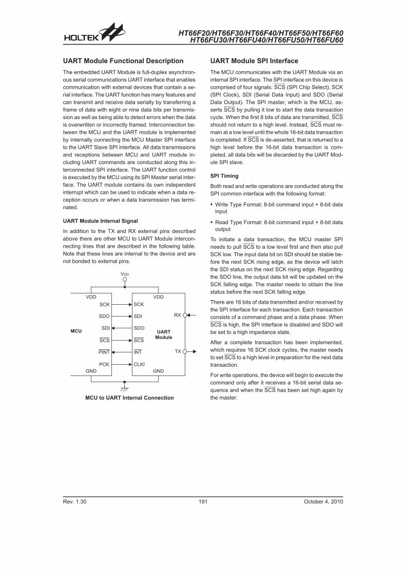
HT66F20/HT66F30/HT66F40/HT66F50/HT66F60HT66FU30/HT66FU40/HT66FU50/HT66FU60
Rev. 1.30 191 October 4, 2010
UART Module Functional Description
The embedded UART Module is full-duplex asynchron-
ous serial communications UART interface that enables
communication with external devices that contain a se-
rial interface. The UART function has many features and
can transmit and receive data serially by transferring a
frame of data with eight or nine data bits per transmis-
sion as well as being able to detect errors when the data
is overwritten or incorrectly framed. Interconnection be-
tween the MCU and the UART module is implemented
by internally connecting the MCU Master SPI interface
to the UART Slave SPI interface. All data transmissions
and receptions between MCU and UART module in-
cluding UART commands are conducted along this in-
terconnected SPI interface. The UART function control
is executed by the MCU using its SPI Master serial inter-
face. The UART module contains its own independent
interrupt which can be used to indicate when a data re-
ception occurs or when a data transmission has termi-
nated.
UART Module Internal Signal
In addition to the TX and RX external pins described
above there are other MCU to UART Module intercon-
necting lines that are described in the following table.
Note that these lines are internal to the device and are
not bonded to external pins.
UART Module SPI Interface
The MCU communicates with the UART Module via an
internal SPI interface. The SPI interface on this device is
comprised of four signals: SCS (SPI Chip Select), SCK
(SPI Clock), SDI (Serial Data Input) and SDO (Serial
Data Output). The SPI master, which is the MCU, as-
serts SCS by pulling it low to start the data transaction
cycle. When the first 8 bits of data are transmitted, SCS
should not return to a high level. Instead, SCS must re-
main at a low level until the whole 16-bit data transaction
is completed. If SCS is de-asserted, that is returned to a
high level before the 16-bit data transaction is com-
pleted, all data bits will be discarded by the UART Mod-
ule SPI slave.
SPI Timing
Both read and write operations are conducted along the
SPI common interface with the following format:
� Write Type Format: 8-bit command input + 8-bit data
input
� Read Type Format: 8-bit command input + 8-bit data
output
To initiate a data transaction, the MCU master SPI
needs to pull SCS to a low level first and then also pull
SCK low. The input data bit on SDI should be stable be-
fore the next SCK rising edge, as the device will latch
the SDI status on the next SCK rising edge. Regarding
the SDO line, the output data bit will be updated on the
SCK falling edge. The master needs to obtain the line
status before the next SCK falling edge.
There are 16 bits of data transmitted and/or received by
the SPI interface for each transaction. Each transaction
consists of a command phase and a data phase. When
SCS is high, the SPI interface is disabled and SDO will
be set to a high impedance state.
After a complete transaction has been implemented,
which requires 16 SCK clock cycles, the master needs
to set SCS to a high level in preparation for the next data
transaction.
For write operations, the device will begin to execute the
command only after it receives a 16-bit serial data se-
quence and when the SCS has been set high again by
the master.
� � �
� � �
� � �
� � �
� � �
� �
� � �
� �
� � �
� � �
� � �
� � �
� � �
� � �
� �
� ! �
�
� � � �
� � � �
� � � �
� � �
MCU to UART Internal Connection

HT66F20/HT66F30/HT66F40/HT66F50/HT66F60HT66FU30/HT66FU40/HT66FU50/HT66FU60
Rev. 1.30 192 October 4, 2010
SDO
SDI
SCK
SCS
A7 A6 A5 A4 A3 A2 A1 A0 D7 D6 D5 D4 D3 D2 D1 D0
Writing Type Format: 8-bit Command Input + 8-bit Data Input
SDO
SDI
SCK
SCS
A7 A6 A5 A4 A3 A2 A1 A0
D7 D6 D5 D4 D3 D2 D1 D0
tw
Reading Type Format: 8-bit Command Input + 8-bit Data Output
For read operations, the device will begin to execute the
command only after it receives an 8-bit read command
after which it will be ready to output data. If necessary,
the master can de-assert the SCS pin to abort the trans-
action at any time which will cause any data transac-
tions to be abandoned.
UART Module External Pin Interfacing
To communicate with an external serial interface, the in-
ternal UART has two external pins known as TX and RX.
The TX pin is the UART transmitter serial data output pin
if the corresponding control bits named UARTEN in
UCR1 register and TXEN in UCR2 register are set to 1.
If the control bit UARTEN or TXEN is equal to zero, the
TX pin is in the state of high impedance. Similarly, the
RX pin is the UART receiver serial data input pin if the
corresponding control bits named UARTEN and RXEN
in UCR1 and UCR2 registers are set to 1. If the control
bit UARTEN or RXEN is equal to zero, the RX pin is in
the state of high impedance.
UART Data Transfer Scheme
The following block diagram shows the overall data
transfer structure arrangement for the UART. The actual
data to be transmitted from the MCU is first transferred
to the TXR register by the application program. The data
will then be transferred to the Transmitter Shift Register
named TSR from where it will be shifted out, LSB first,
onto the TX pin at a rate controlled by the Baud Rate
Generator. Only the TXR register is accessible to the
application program, the Transmitter Shift Register is
not mapped into the Data Memory area and is inacces-
sible to the application program.
Data to be received by the UART is accepted on the ex-
ternal RX pin, from where it is shifted in, LSB first, to the
Receiver Shift Register named RSR at a rate controlled
by the Baud Rate Generator. When the shift register is
full, the data will then be transferred from the shift regis-
ter to the internal RXR register, where it is buffered and
can be manipulated by the application program. Only
the RXR register is accessible to the application pro-
gram, the Receiver Shift Register is not mapped into the
Data Memory area and is inaccessible to the application
program. It should be noted that the actual register for
data transmission and reception, although referred to in
the text, and in application programs, as separate TXR
and RXR registers, only exists as a single shared regis-
ter physically. This shared register known as the
TXR/RXR register is used for both data transmission
and data reception.
MSB LSB
Transmitter Shift Register (TSR)
MSB LSB
Receiver Shift Register (RSR)
TX Pin RX Pin
Baud Rate
GeneratorTX Register (TXR) RX Register (RXR)
Buffer 1
Buffer 2
Buffer 3
Data to be transmitted Data received
UART Data Transfer Scheme

HT66F20/HT66F30/HT66F40/HT66F50/HT66F60HT66FU30/HT66FU40/HT66FU50/HT66FU60
Rev. 1.30 193 October 4, 2010
UART Commands
There are both read and write commands for the UART Module. For reading and writing to registers both command and
address information is contained within a single byte. The format for reading and writing is shown in the following table.
Command Type Bit 7 Bit 6 Bit 5 Bit 4 Bit 3 Bit 2 Bit 1 Bit 0
Read FIFO 0 0 0 0 0 X X X
Read Register 0 0 0 1 0 A2 A1 A0
Write FIFO 0 0 0 0 1 X X X
Write Register 0 0 0 1 1 A2 A1 A0
Note: �X� here stands for �dont care�
UART Status and Control Registers
There are six registers associated with the UART function. The USR, UCR1, UCR2 and UCR3 registers control the
overall function of the UART module, while the BRG register controls the Baud rate. The actual data to be transmitted
and received on the serial interface is managed through the TXR/RXR data register.
A[2:0] Name Reset Bit 7 Bit 6 Bit 5 Bit 4 Bit 3 Bit 2 Bit 1 Bit 0
00H USR 0000 1011 PERR NF FERR OERR RIDLE RXIF TIDLE TXIF
01H UCR1 0000 0X00 UARTEN BNO PREN PRT STOPS TXBRK RX8 TX8
02H UCR2 0000 0000 TXEN RXEN BRGH ADDEN WAKE RIE TIIE TEIE
03H BRG XXXX XXXX BRG7 BRG6 BRG5 BRG4 BRG3 BRG2 BRG1 BRG0
04H UCR3 0��� ���� URST � � � � � � �
05H~
07HUnused ���� ���� Reserved
UART Register Summary
� USR Register
The USR register is the status register for the UART, which can be read by the application program to determine the
present status of the UART. All flags within the USR register are read only. Further explanation on each of the flags is
given below:
Bit 7 6 5 4 3 2 1 0
Name PERR NF FERR OERR RIDLE RXIF TIDLE TXIF
R/W R R R R R R R R
POR 0 0 0 0 1 0 1 1
Bit 7 PERR: Parity error flag
0: no parity error is detected
1: parity error is detected
The PERR flag is the parity error flag. When this read only flag is �0�, it indicates a parity error
has not been detected. When the flag is �1�, it indicates that the parity of the received word is
incorrect. This error flag is applicable only if Parity mode (odd or even) is selected. The flag can
also be cleared by a software sequence which involves a read to the status register USR
followed by an access to the RXR data register.
Bit 6 NF: Noise flag
0: no noise is detected
1: noise is detected
The NR flag is the noise flag. When this read only flag is �0�, it indicates no noise condition.
When the flag is �1�, it indicates that the UART has detected noise on the receiver input.
The NF flag is set during the same cycle as the RXIF flag but will not be set in the case of as
overrun. The NF flag can be cleared by a software sequence which will involve a read to the
status register USR followed by an access to the RXR data register.

HT66F20/HT66F30/HT66F40/HT66F50/HT66F60HT66FU30/HT66FU40/HT66FU50/HT66FU60
Rev. 1.30 194 October 4, 2010
Bit 5 FERR: Framing error flag
0: no framing error is detected
1: framing error is detected
The FERR flag is the framing error flag. When this read only flag is �0�, it indicates that there
is no framing error. When the flag is �1�, it indicates that a framing error has been detected
for the current character. The flag can also be cleared by a software sequence which will involve
a read to the status register USR followed by an access to the RXR data register.
Bit 4 OERR: Overrun error flag
0: no overrun error is detected
1: overrun error is detected
The OERR flag is the overrun error flag which indicates when the receiver buffer has overflowed.
When this read only flag is �0�, it indicates that there is no overrun error. When the flag is
�1�, it indicates that an overrun error occurs which will inhibit further transfers to the RXR
receive data register. The flag is cleared by a software sequence, which is a read to the status
register USR followed by an access to the RXR data register.
Bit 3 RIDLE: Receiver status
0: data reception is in progress (data being received)
1: no data reception is in progress (receiver is idle)
The RIDLE flag is the receiver status flag. When this read only flag is �0�, it indicates that the
receiver is between the initial detection of the start bit and the completion of the stop bit. When
the flag is �1�, it indicates that the receiver is idle. Between the completion of the stop bit and
the detection of the next start bit, the RIDLE bit is �1� indicating that the UART receiver is idle
and the RX pin stays in logic high condition.
Bit 2 RXIF: Receive RXR data register status
0: RXR data register is empty
1: RXR data register has available data
The RXIF flag is the receive data register status flag. When this read only flag is �0�, it indicates
that the RXR read data register is empty. When the flag is �1�, it indicates that the RXR read data
register contains new data. When the contents of the shift register are transferred to the RXR
register, an interrupt is generated if RIE=1 in the UCR2 register. If one or more errors are
detected in the received word, the appropriate receive-related flags NF, FERR, and/or PERR are
set within the same clock cycle. The RXIF flag is cleared when the USR register is read with
RXIF set, followed by a read from the RXR register, and if the RXR register has no data
available.
Bit 1 TIDLE: Transmission idle
0: data transmission is in progress (data being transmitted)
1: no data transmission is in progress (transmitter is idle)
The TIDLE flag is known as the transmission complete flag. When this read only flag is �0�, it
indicates that a transmission is in progress. This flag will be set to �1� when the TXIF flag is
�1� and when there is no transmit data or break character being transmitted. When TIDLE is
equal to �1�, the TX pin becomes idle with the pin state in logic high condition. The TIDLE flag is
cleared by reading the USR register with TIDLE set and then writing to the TXR register. The flag
is not generated when a data character or a break is queued and ready to be sent.
Bit 0 TXIF: Transmit TXR data register status
0: character is not transferred to the transmit shift register
1: character has transferred to the transmit shift register (TXR data register is empty)
The TXIF flag is the transmit data register empty flag. When this read only flag is �0�, it
indicates that the character is not transferred to the transmitter shift register. When the flag is
�1�, it indicates that the transmitter shift register has received a character from the TXR data
register. The TXIF flag is cleared by reading the UART status register (USR) with TXIF set and
then writing to the TXR data register. Note that when the TXEN bit is set, the TXIF flag bit will
also be set since the transmit data register is not yet full.

HT66F20/HT66F30/HT66F40/HT66F50/HT66F60HT66FU30/HT66FU40/HT66FU50/HT66FU60
Rev. 1.30 195 October 4, 2010
� UCR1 register
The UCR1 register together with the UCR2 register are the two UART control registers that are used to set the vari-
ous options for the UART function such as overall on/off control, parity control, data transfer bit length, etc. Further
explanation on each of the bits is given below:
Bit 7 6 5 4 3 2 1 0
Name UARTEN BNO PREN PRT STOPS TXBRK RX8 TX8
R/W R/W R/W R/W R/W R/W R/W R W
POR 0 0 0 0 0 0 X 0
�x� unknown
Bit 7 UARTEN: UART function enable control
0: disable UART. TX and RX pins are in the state of high impedance
1: enable UART. TX and RX pins function as UART pins
The UARTEN bit is the UART enable bit. When this bit is equal to �0�, the UART will be
disabled and the RX pin as well as the TX pin will be in the state of high impedance. When the
bit is equal to �1�, the UART will be enabled and the TX and RX pins will function as defined by
the TXEN and RXEN enable control bits. When the UART is disabled, it will empty the buffer so
any character remaining in the buffer will be discarded. In addition, the value of the baud rate
counter will be reset. If the UART is disabled, all error and status flags will be reset. Also the
TXEN, RXEN, TXBRK, RXIF, OERR, FERR, PERR and NF bits will be cleared, while the TIDLE,
TXIF and RIDLE bits will be set. Other control bits in UCR1, UCR2 and BRG registers will remain
unaffected. If the UART is active and the UARTEN bit is cleared, all pending transmissions and
receptions will be terminated and the module will be reset as defined above. When the UART is
re-enabled, it will restart in the same configuration.
Bit 6 BNO: Number of data transfer bits selection
0: 8-bit data transfer
1: 9-bit data transfer
This bit is used to select the data length format, which can have a choice of either 8-bit or 9-bit
format. When this bit is equal to �1�, a 9-bit data length format will be selected. If the bit is
equal to �0�, then an 8-bit data length format will be selected. If 9-bit data length format is
selected, then bits RX8 and TX8 will be used to store the 9th bit of the received and transmitted
data respectively.
Bit 5 PREN: Parity function enable control
0: parity function is disabled
1: parity function is enabled
This is the parity enable bit. When this bit is equal to �1�, the parity function will be enabled. If
the bit is equal to �0�, then the parity function will be disabled.
Bit 4 PRT: Parity type selection bit
0: even parity for parity generator
1: odd parity for parity generator
This bit is the parity type selection bit. When this bit is equal to �1�, odd parity type will be
selected. If the bit is equal to �0�, then even parity type will be selected.
Bit 3 STOPS: Number of Stop bits selection
0: one stop bit format is used
1: two stop bits format is used
This bit determines if one or two stop bits are to be used. When this bit is equal to �1�, two
stop bits are used. If this bit is equal to �0�, then only one stop bit is used.
Bit 2 TXBRK: Transmit break character
0: no break character is transmitted
1: break characters transmit
The TXBRK bit is the Transmit Break Character bit. When this bit is �0�, there are no break
characters and the TX pin operates normally. When the bit is �1�, there are transmit break
characters and the transmitter will send logic zeros. When this bit is equal to �1�, after the
buffered data has been transmitted, the transmitter output is held low for a minimum of a 13-bit
length and until the TXBRK bit is reset.

HT66F20/HT66F30/HT66F40/HT66F50/HT66F60HT66FU30/HT66FU40/HT66FU50/HT66FU60
Rev. 1.30 196 October 4, 2010
Bit 1 RX8: Receive data bit 8 for 9-bit data transfer format (read only)
This bit is only used if 9-bit data transfers are used, in which case this bit location will store the
9th bit of the received data known as RX8. The BNO bit is used to determine whether data
transfers are in 8-bit or 9-bit format.
Bit 0 TX8: Transmit data bit 8 for 9-bit data transfer format (write only)
This bit is only used if 9-bit data transfers are used, in which case this bit location will store the
9th bit of the transmitted data known as TX8. The BNO bit is used to determine whether data
transfers are in 8-bit or 9-bit format.
� UCR2 register
The UCR2 register is the second of the UART control registers and serves several purposes. One of its main func-
tions is to control the basic enable/disable operation if the UART Transmitter and Receiver as well as enabling the
various UART interrupt sources. The register also serves to control the baud rate speed, receiver wake-up function
enable and the address detect function enable. Further explanation on each of the bits is given below:
Bit 7 6 5 4 3 2 1 0
Name TXEN RXEN BRGH ADDEN WAKE RIE TIIE TEIE
R/W R/W R/W R/W R/W R/W R/W R W
POR 0 0 0 0 1 0 1 1
Bit 7 TXEN: UART Transmitter enable control
0: UART transmitter is disabled
1: UART transmitter is enabled
The bit named TXEN is the Transmitter Enable Bit. When this bit is equal to �0�, the transmitter
will be disabled with any pending data transmissions being aborted. In addition the buffers will be
reset. In this situation the TX pin will be in the state of high impedance. If the TXEN bit is equal to
�1� and the UARTEN bit is also equal to �1�, the transmitter will be enabled and the TX pin will
be controlled by the UART. Clearing the TXEN bit during a transmission will cause the data
transmission to be aborted and will reset the transmitter. If this situation occurs, the TX pin will
be in the state of high impedance.
Bit 6 RXEN: UART Receiver enable control
0: UART receiver is disabled
1: UART receiver is enabled
The bit named RXEN is the Receiver Enable Bit. When this bit is equal to �0�, the receiver will
be disabled with any pending data receptions being aborted. In addition the receive buffers will
be reset. In this situation the RX pin will be in the state of high impedance. If the RXEN bit is
equal to �1� and the UARTEN bit is also equal to �1�, the receiver will be enabled and the RX pin
will be controlled by the UART. Clearing the RXEN bit during a reception will cause the data
reception to be aborted and will reset the receiver. If this situation occurs, the RX pin will be in the
state of high impedance.
Bit 5 BRGH: Baud Rate speed selection
0: low speed baud rate
1: high speed baud rate
The bit named BRGH selects the high or low speed mode of the Baud Rate Generator. This bit,
together with the value placed in the baud rate register BRG, controls the Baud Rate of the
UART. If this bit is equal to �1�, the high speed mode is selected. If the bit is equal to �0�,
the low speed mode is selected.
Bit 4 ADDEN: Address detect function enable control
0: address detect function is disabled
1: address detect function is enabled
The bit named ADDEN is the address detect function enable control bit. When this bit is equal to
�1�, the address detect function is enabled. When it occurs, if the 8th bit, which corresponds to
RX7 if BNO=0 or the 9th bit, which corresponds to RX8 if BNO=1, has a value of �1�,
then the received word will be identified as an address, rather than data. If the corresponding
interrupt is enabled, an interrupt request will be generated each time the received word has the
address bit set, which is the 8th or 9th bit depending on the value of BNO. If the address bit
known as the 8th or 9th bit of the received word is �0� with the address detect function being
enabled, an interrupt will not be generated and the received data will be discarded.

HT66F20/HT66F30/HT66F40/HT66F50/HT66F60HT66FU30/HT66FU40/HT66FU50/HT66FU60
Rev. 1.30 197 October 4, 2010
Bit 3 WAKE: RX pin falling edge wake-up function enable control
0: RX pin wake-up function is disabled
1: RX pin wake-up function is enabled
This bit enables or disables the receiver wake-up function. If this bit is equal to �1� and the
MCU is in IDLE or SLEEP mode, a falling edge on the RX input pin will wake-up
the device. If this bit is equal to �0� and the MCU is in IDLE or SLEEP mode,
any edge transitions on the RX pin will not wake-up the device.
Bit 2 RIE: Receiver interrupt enable control
0: receiver related interrupt is disabled
1: receiver related interrupt is enabled
This bit enables or disables the receiver interrupt. If this bit is equal to �1� and when the
receiver overrun flag OERR or receive data available flag RXIF is set, the UART interrupt request
flag will be set. If this bit is equal to �0�, the UART interrupt request flag will not be influenced
by the condition of the OERR or RXIF flags.
Bit 1 TIIE: Transmitter Idle interrupt enable control
0: transmitter idle interrupt is disabled
1: transmitter idle interrupt is enabled
This bit enables or disables the transmitter idle interrupt. If this bit is equal to �1� and when
the transmitter idle flag TIDLE is set, due to a transmitter idle condition, the UART interrupt
request flag will be set. If this bit is equal to �0�, the UART interrupt request flag will not be
influenced by the condition of the TIDLE flag.
Bit 0 TEIE: Transmitter Empty interrupt enable control
0: transmitter empty interrupt is disabled
1: transmitter empty interrupt is enabled
This bit enables or disables the transmitter empty interrupt. If this bit is equal to �1� and when
the transmitter empty flag TXIF is set, due to a transmitter empty condition, the UART interrupt
request flag will be set. If this bit is equal to �0�, the UART interrupt request flag will not be
influenced by the condition of the TXIF flag.
� UCR3 register
The UCR3 register is the last of the UART control registers and controls the software reset operation of the UART
module. The only one available bit named URST in the UART control register UCR3 is the UART software reset con-
trol bit. When this bit is equal to �0�, the UART operates normally. If this bit is equal to �1�, the whole UART module
will be reset. When this situation occurs, the transmitter and receiver will be reset. The UART registers including the
status register and control registers will keep the POR states shown in the above UART registers table after the reset
condition occurs.
Bit 7 6 5 4 3 2 1 0
Name URST � � � � � � �
R/W R/W � � � � � � �
POR 0 � � � � � � �
Bit 7 URST: UART software reset
0: no action
1: UART reset occurs
Bit 6~0 unimplemented, read as �0�

HT66F20/HT66F30/HT66F40/HT66F50/HT66F60HT66FU30/HT66FU40/HT66FU50/HT66FU60
Rev. 1.30 198 October 4, 2010
Baud Rate Generator
To setup the speed of the serial data communication,
the UART function contains its own dedicated baud rate
generator. The baud rate is controlled by its own internal
free running 8-bit timer, the period of which is deter-
mined by two factors. The first of these is the value
placed in the baud rate register BRG and the second is
the value of the BRGH bit with the control register
UCR2. The BRGH bit decides if the baud rate generator
is to be used in a high speed mode or low speed mode,
which in turn determines the formula that is used to cal-
culate the baud rate. The value N in the BRG register
which is used in the following baud rate calculation for-
mula determines the division factor. Note that N is the
decimal value placed in the BRG register and has a
range of between 0 and 255.
UCR2 BRGH Bit 0 1
Baud Rate (BR)f
[64 (N+1)]
CLKI f
[16 (N+1)]
CLKI
By programming the BRGH bit which allows selection of
the related formula and programming the required value
in the BRG register, the required baud rate can be
setup. Note that because the actual baud rate is deter-
mined using a discrete value, N, placed in the BRG reg-
ister, there will be an error associated between the
actual and requested value. The following example
shows how the BRG register value N and the error value
can be calculated.
� Calculating the baud rate and error values
For a clock frequency of 4MHz, and with BRGH set to
�0� determine the BRG register value N, the actual
baud rate and the error value for a desired baud rate
of 4800.
From the above table the desired baud rate BR =f
[64 (N+1)]
CLKI
Re-arranging this equation gives N =f
(BRx64)
CLKI � 1
Giving a value for N =4000000
4800 64( )x
� 1 � 12.0208
To obtain the closest value, a decimal value of 12 should
be placed into the BRG register. This gives an actual or
calculated baud rate value of BR=4000000
[64(12+1)]� 4808
Therefore the error is equal to = 0.16%� ! # ! � � � � ! # #
� ! # #
The following tables show the actual values of baud rate and error values for the two value of BRGH.
Baud Rate
K/BPS
Baud Rates for BRGH=0
fCLKI=4MHz fCLKI=7.159MHz
BRG Kbaud Error (%) BRG Kbaud Error (%)
0.3 207 0.300 0.00 185 0.300 0.00
1.2 51 1.202 0.16 46 1.190 �0.83
2.4 25 2.404 0.16 22 2.432 1.32
4.8 12 4.808 0.16 11 4.661 �2.90
9.6 6 8.929 �6.99 5 9.321 �2.90
19.2 2 20.830 8.51 2 18.643 �2.90
38.4 1 � � 1 � �
57.6 0 62.500 8.51 0 55.930 �2.90
115.2 � � � � � �
Baud Rates and Error Values for BRGH � 0

HT66F20/HT66F30/HT66F40/HT66F50/HT66F60HT66FU30/HT66FU40/HT66FU50/HT66FU60
Rev. 1.30 199 October 4, 2010
Baud Rate
K/BPS
Baud Rates for BRGH=1
fCLKI=4MHz fCLKI=7.159MHz
BRG Kbaud Error (%) BRG Kbaud Error (%)
0.3 � � � � � �
1.2 207 1.202 0.16 185 1.203 0.23
2.4 103 2.404 0.16 92 2.406 0.23
4.8 51 4.808 0.16 46 4.760 �0.83
9.6 25 9.615 0.16 22 9.727 1.32
19.2 12 19.231 0.16 11 18.643 �2.90
38.4 6 35.714 �6.99 5 37.286 �2.90
57.6 3 62.5 8.51 3 55.930 �2.90
115.2 1 125 8.51 1 111.86 �2.90
250 0 250 0 � � �
Baud Rates and Error Values for BRGH � 1
� BRG Register
Bit 7 6 5 4 3 2 1 0
Name BRG7 BRG6 BRG5 BRG4 BRG3 BRG2 BRG1 BRG0
R/W R/W R/W R/W R/W R/W R/W R/W R/W
POR x x x x x x x x
�x�: unknown
Bit 7~0 BRG7~BRG0: Baud Rate values
By programming the BRGH bit in UCR2 Register which allows selection of the related formula
described above and programming the required value in the BRG register, the required baud rate
can be setup.

HT66F20/HT66F30/HT66F40/HT66F50/HT66F60HT66FU30/HT66FU40/HT66FU50/HT66FU60
Rev. 1.30 200 October 4, 2010
UART Module Setup and Control
For data transfer, the UART function utilizes a
non-return-to-zero, more commonly known as NRZ, for-
mat. This is composed of one start bit, eight or nine data
bits and one or two stop bits. Parity is supported by the
UART hardware and can be setup to be even, odd or no
parity. For the most common data format, 8 data bits
along with no parity and one stop bit, denoted as 8, N, 1,
is used as the default setting, which is the setting at
power-on. The number of data bits and stop bits, along
with the parity, are setup by programming the corre-
sponding BNO, PRT, PREN and STOPS bits in the
UCR1 register. The baud rate used to transmit and re-
ceive data is setup using the internal 8-bit baud rate
generator, while the data is transmitted and received
LSB first. Although the transmitter and receiver of the
UART are functionally independent, they both use the
same data format and baud rate. In all cases stop bits
will be used for data transmission.
� Enabling/Disabling the UART
The basic on/off function of the internal UART function
is controlled using the UARTEN bit in the UCR1 regis-
ter. If the UARTEN, TXEN and RXEN bits are set, then
these two UART pins will act as normal TX output pin
and RX input pin respectively. If no data is being trans-
mitted on the TX pin, then it will default to a logic high
value.
Clearing the UARTEN bit will disable the TX and RX
pins and these two pins will be in the state of high im-
pedance. When the UART function is disabled, the
buffer will be reset to an empty condition, at the same
time discarding any remaining residual data. Dis-
abling the UART will also reset the enable control, the
error and status flags with bits TXEN, RXEN, TXBRK,
RXIF, OERR, FERR, PERR and NF being cleared
while bits TIDLE, TXIF and RIDLE will be set. The re-
maining control bits in the UCR1, UCR2 and BRG reg-
isters will remain unaffected. If the UARTEN bit in the
UCR1 register is cleared while the UART is active,
then all pending transmissions and receptions will be
immediately suspended and the UART will be reset to
a condition as defined above. If the UART is then sub-
sequently re-enabled, it will restart again in the same
configuration.
� Data, parity and stop bit selection
The format of the data to be transferred is composed
of various factors such as data bit length, parity on/off,
parity type, address bits and the number of stop bits.
These factors are determined by the setup of various
bits within the UCR1 register. The BNO bit controls the
number of data bits which can be set to either 8 or 9.
The PRT bit controls the choice if odd or even parity.
The PREN bit controls the parity on/off function. The
STOPS bit decides whether one or two stop bits are to
be used. The following table shows various formats
for data transmission. The address detect mode con-
trol bit identifies the frame as an address character.
The number of stop bits, which can be either one or
two, is independent of the data length.
Start
Bit
Data
Bits
Address
Bits
Parity
Bits
Stop
Bit
Example of 8-bit Data Formats
1 8 0 0 1
1 7 0 1 1
1 7 1 0 1
Example of 9-bit Data Formats
1 9 0 0 1
1 8 0 1 1
1 8 1 0 1
Transmitter Receiver Data Format
The following diagram shows the transmit and receive
waveforms for both 8-bit and 9-bit data formats.
� � � � � � $ / � $ / � � # $ / � � � $ / � � � $ / � � � $ / � � � $ / � � � $ / � � � $ / � � � � 0 1 � $ / �
� 2 �� � � � �$ / �
� � � / � 3 � $ / �
� � " # $ � � % $ % � � � & ' % $
� � � � � � $ / � $ / � � # $ / � � � $ / � � � $ / � � � $ / � � � $ / � � � $ / � � � $ / � � � � 0 1 � $ / �
� 2 �� � � � �$ / �
� � � / � 3 � $ / �
( � " # $ � � % $ % � � � & ' % $
$ / � � !

HT66F20/HT66F30/HT66F40/HT66F50/HT66F60HT66FU30/HT66FU40/HT66FU50/HT66FU60
Rev. 1.30 201 October 4, 2010
� UART transmitter
Data word lengths of either 8 or 9 bits can be selected
by programming the BNO bit in the UCR1 register.
When BNO bit is set, the word length will be set to 9
bits. In this case the 9th bit, which is the MSB, needs
to be stored in the TX8 bit in the UCR1 register. At the
transmitter core lies the Transmitter Shift Register,
more commonly known as the TSR, whose data is ob-
tained from the transmit data register, which is known
as the TXR register. The data to be transmitted is
loaded into this TXR register by the application pro-
gram. The TSR register is not written to with new data
until the stop bit from the previous transmission has
been sent out. As soon as this stop bit has been trans-
mitted, the TSR can then be loaded with new data
from the TXR register, if it is available. It should be
noted that the TSR register, unlike many other regis-
ters, is not directly mapped into the Data Memory area
and as such is not available to the application program
for direct read/write operations. An actual transmis-
sion of data will normally be enabled when the TXEN
bit is set, but the data will not be transmitted until the
TXR register has been loaded with data and the baud
rate generator has defined a shift clock source. How-
ever, the transmission can also be initiated by first
loading data into the TXR register, after which the
TXEN bit can be set. When a transmission of data be-
gins, the TSR is normally empty, in which case a
transfer to the TXR register will result in an immediate
transfer to the TSR. If during a transmission the TXEN
bit is cleared, the transmission will immediately cease
and the transmitter will be reset. The TX output pin will
then return to the high impedance state.
� Transmitting data
When the UART is transmitting data, the data is
shifted on the TX pin from the shift register, with the
least significant bit LSB first. In the transmit mode, the
TXR register forms a buffer between the internal bus
and the transmitter shift register. It should be noted
that if 9-bit data format has been selected, then the
MSB will be taken from the TX8 bit in the UCR1 regis-
ter. The steps to initiate a data transfer can be sum-
marized as follows:
� Make the correct selection of the BNO, PRT, PREN
and STOPS bits to define the required word length,
parity type and number of stop bits.
� Setup the BRG register to select the desired baud
rate.
� Set the TXEN bit to ensure that the UART transmit-
ter is enabled and the TX pin is used as a UART
transmitter pin.
� Access the USR register and write the data that is to
be transmitted into the TXR register. Note that this
step will clear the TXIF bit.
This sequence of events can now be repeated to send
additional data.
It should be noted that when TXIF=0, data will be in-
hibited from being written to the TXR register. Clear-
ing the TXIF flag is always achieved using the
following software sequence:
1. A USR register access
2. A TXR register write execution
The read-only TXIF flag is set by the UART hardware
and if set indicates that the TXR register is empty and
that other data can now be written into the TXR regis-
ter without overwriting the previous data. If the TEIE
bit is set, then the TXIF flag will generate an interrupt.
During a data transmission, a write instruction to the
TXR register will place the data into the TXR register,
which will be copied to the shift register at the end of
the present transmission. When there is no data
transmission in progress, a write instruction to the
TXR register will place the data directly into the shift
register, resulting in the commencement of data trans-
mission, and the TXIF bit being immediately set.
When a frame transmission is complete, which hap-
pens after stop bits are sent or after the break frame,
the TIDLE bit will be set. To clear the TIDLE bit the fol-
lowing software sequence is used:
1. A USR register access
2. A TXR register write execution
Note that both the TXIF and TIDLE bits are cleared by
the same software sequence.
� Transmitting break
If the TXBRK bit is set, then the break characters will
be sent on the next transmission. Break character
transmission consists of a start bit, followed by 13�N
�0� bits, where N=1, 2, etc. if a break character is to be
transmitted, then the TXBRK bit must be first set by
the application program and then cleared to generate
the stop bits. Transmitting a break character will not
generate a transmit interrupt. Note that a break condi-
tion length is at least 13 bits long. If the TXBRK bit is
continually kept at a logic high level, then the transmit-
ter circuitry will transmit continuous break characters.
After the application program has cleared the TXBRK
bit, the transmitter will finish transmitting the last break
character and subsequently send out one or two stop
bits. The automatic logic high at the end of the last
break character will ensure that the start bit of the next
frame is recognized.

HT66F20/HT66F30/HT66F40/HT66F50/HT66F60HT66FU30/HT66FU40/HT66FU50/HT66FU60
Rev. 1.30 202 October 4, 2010
� UART receiver
The UART is capable of receiving word lengths of ei-
ther 8 or 9 bits can be selected by programming the
BNO bit in the UCR1 register. When BNO bit is set, the
word length will be set to 9 bits. In this case the 9th bit,
which is the MSB, will be stored in the RX8 bit in the
UCR1 register. At the receiver core lies the Receiver
Shift Register more commonly known as the RSR.
The data which is received on the RX external input
pin is sent to the data recovery block. The data recov-
ery block operating speed is 16 times that of the baud
rate, while the main receive serial shifter operates at
the baud rate. After the RX pin is sampled for the stop
bit, the received data in RSR is transferred to the re-
ceive data register, if the register is empty. The data
which is received on the external RX input pin is sam-
pled three times by a majority detect circuit to deter-
mine the logic level that has been placed onto the RX
pin. It should be noted that the RSR register, unlike
many other registers, is not directly mapped into the
Data Memory area and as such is not available to the
application program for direct read/write operations.
� Receiving data
When the UART receiver is receiving data, the data is
serially shifted in on the external RX input pin to the
shift register, with the least significant bit LSB first.
The RXR register is a four byte deep FIFO data buffer,
where four bytes can be held in the FIFO while the 5th
byte can continue to be received. Note that the appli-
cation program must ensure that the data is read from
RXR before the 5th byte has been completely shifted
in, otherwise the 5th byte will be discarded and an
overrun error OERR will be subsequently indicated.
The steps to initiate a data transfer can be summa-
rized as follows:
� Make the correct selection of the BNO, PRT, PREN
and STOPS bits to define the required word length,
parity type and number of stop bits.
� Setup the BRG register to select the desired baud
rate.
� Set the RXEN bit to ensure that the UART receiver
is enabled and the RX pin is used as a UART re-
ceiver pin.
At this point the receiver will be enabled which will be-
gin to look for a start bit.
When a character is received, the following sequence
of events will occur:
� The RXIF bit in the USR register will be set then
RXR register has data available, at least three more
character can be read.
� When the contents of the shift register have been
transferred to the RXR register and if the RIE bit is
set, then an interrupt will be generated.
� If during reception, a frame error, noise error, parity
error or an overrun error has been detected, then
the error flags can be set.
The RXIF bit can be cleared using the following soft-
ware sequence:
1. A USR register access
2. A RXR register read execution
� Receiving break
Any break character received by the UART will be
managed as a framing error. The receiver will count
and expect a certain number of bit times as specified
by the values programmed into the BNO and STOPS
bits. If the break is much longer than 13 bit times, the
reception will be considered as complete after the
number of bit times specified by BNO and STOPS.
The RXIF bit is set, FERR is set, zeros are loaded into
the receive data register, interrupts are generated if
appropriate and the RIDLE bit is set. If a long break
signal has been detected and the receiver has re-
ceived a start bit, the data bits and the invalid stop bit,
which sets the FERR flag, the receiver must wait for a
valid stop bit before looking for the next start bit. The
receiver will not make the assumption that the break
condition on the line is the next start bit. A break is re-
garded as a character that contains only zeros with
the FERR flag set. The break character will be loaded
into the buffer and no further data will be received until
stop bits are received. It should be noted that the
RIDLE read only flag will go high when the stop bits
have not yet been received. The reception of a break
character on the UART registers will result in the fol-
lowing:
� The framing error flag, FERR, will be set.
� The receive data register, RXR, will be cleared.
� The OERR, NF, PERR, RIDLE or RXIF flags will
possibly be set.
� Idle status
When the receiver is reading data, which means it will
be in between the detection of a start bit and the read-
ing of a stop bit, the receiver status flag in the USR
register, otherwise known as the RIDLE flag, will have
a zero value. In between the reception of a stop bit
and the detection of the next start bit, the RIDLE flag
will have a high value, which indicates the receiver is
in an idle condition.
� Receiver interrupt
The read only receive interrupt flag RXIF in the USR
register is set by an edge generated by the receiver.
An interrupt is generated if RIE=1, when a word is
transferred from the Receive Shift Register, RSR, to
the Receive Data Register, RXR. An overrun error can
also generate an interrupt if RIE=1.

HT66F20/HT66F30/HT66F40/HT66F50/HT66F60HT66FU30/HT66FU40/HT66FU50/HT66FU60
Rev. 1.30 203 October 4, 2010
Managing Receiver Errors
Several types of reception errors can occur within the
UART module, the following section describes the vari-
ous types and how they are managed by the UART.
� Overrun Error � OERR flag
The RXR register is composed of a four byte deep
FIFO data buffer, where four bytes can be held in the
FIFO register, while a 5th byte can continue to be re-
ceived. Before the 5th byte has been entirely shifted
in, the data should be read from the RXR register. If
this is not done, the overrun error flag OERR will be
consequently indicated.
In the event of an overrun error occurring, the follow-
ing will happen:
� The OERR flag in the USR register will be set.
� The RXR contents will not be lost.
� The shift register will be overwritten.
� An interrupt will be generated if the RIE bit is set.
The OERR flag can be cleared by an access to the
USR register followed by a read to the RXR register.
� Noise Error � NF flag
Over-sampling is used for data recovery to identify
valid incoming data and noise. If noise is detected
within a frame, the following will occur:
� The read only noise flag, NF, in the USR register
will be set on the rising edge of the RXIF bit.
� Data will be transferred from the shift register to the
RXR register.
� No interrupt will be generated. However this bit
rises at the same time as the RXIF bit which itself
generates an interrupt.
Note that the NF flag is reset by a USR register read
operation followed by an RXR register read operation.
� Framing Error � FERR flag
The read only framing error flag, FERR, in the USR
register, is set if a zero is detected instead of stop bits.
If two stop bits are selected, both stop bits must be
high. Otherwise the FERR flag will be set. The FERR
flag is buffered along with the received data and is
cleared in any reset.
� Parity Error � PERR flag
The read only parity error flag, PERR, in the USR reg-
ister, is set if the parity of the received word is incor-
rect. This error flag is only applicable if the parity
function is enabled, PREN=1, and if the parity type,
odd or even, is selected. The read only PERR flag is
buffered along with the received data bytes. It is
cleared on any reset, it should be noted that the FERR
and PERR flags are buffered along with the corre-
sponding word and should be read before reading the
data word.
UART Module Interrupt Structure
Several individual UART conditions can generate a
UART interrupt. When these conditions exist, a low
pulse will be generated on the INT line to get the atten-
tion of the microcontroller. These conditions are a trans-
mitter data register empty, transmitter idle, receiver data
available, receiver overrun, address detect and an RX
pin wake-up. When any of these conditions are created,
if its corresponding interrupt control is enabled and the
stack is not full, the program will jump to its correspond-
ing interrupt vector where it can be serviced before re-
turning to the main program. Four of these conditions
have the corresponding USR register flags which will
generate a UART interrupt if its associated interrupt en-
able control bit in the UCR2 register is set. The two
transmitter interrupt conditions have their own corre-
sponding enable control bits, while the two receiver in-
terrupt conditions have a shared enable control bit.
These enable bits can be used to mask out individual
UART interrupt sources.
The address detect condition, which is also a UART in-
terrupt source, does not have an associated flag, but will
generate a UART interrupt when an address detect con-
dition occurs if its function is enabled by setting the
ADDEN bit in the UCR2 register. An RX pin wake-up,
which is also a UART interrupt source, does not have an
associated flag, but will generate a UART interrupt if the
microcontroller is woken up by a falling edge on the RX
pin, if the WAKE and RIE bits in the UCR2 register are
set. Note that in the event of an RX wake-up interrupt
occurring, there will be a certain period of delay, com-
monly known as the System Start-up Time, for the oscil-
lator to restart and stabilize before the system resumes
normal operation.
Note that the USR register flags are read only and can-
not be cleared or set by the application program, neither
will they be cleared when the program jumps to the cor-
responding interrupt servicing routine, as is the case for
some of the other interrupts. The flags will be cleared
automatically when certain actions are taken by the
UART, the details of which are given in the UART regis-
ter section. The overall UART interrupt can be disabled
or enabled by the related interrupt enable control bits in
the interrupt control registers of the microcontroller to
decide whether the interrupt requested by the UART
module is masked out or allowed.

HT66F20/HT66F30/HT66F40/HT66F50/HT66F60HT66FU30/HT66FU40/HT66FU50/HT66FU60
Rev. 1.30 204 October 4, 2010
� Address detect mode
Setting the Address Detect function enable control bit,
ADDEN, in the UCR2 register, enables this special
function. If this bit is set to �1�, then an additional qual-
ifier will be placed on the generation of a Receiver
Data Available interrupt, which is requested by the
RXIF flag. If the ADDEN bit is equal to �1�, then when
the data is available, an interrupt will only be gener-
ated, if the highest received bit has a high value. Note
that the related interrupt enable control bit and the
EMI bit of the microcontroller must also be enabled for
correct interrupt generation. The highest address bit is
the 9th bit if the bit BNO=1 or the 8th bit if the bit
BNO=0. If the highest bit is high, then the received
word will be defined as an address rather than data. A
Data Available interrupt will be generated every time
the last bit of the received word is set. If the ADDEN bit
is equal to �0�, then a Receive Data Available interrupt
will be generated each time the RXIF flag is set, irre-
spective of the data last but status. The address de-
tect and parity functions are mutually exclusive
functions. Therefore if the address detect function is
enabled, then to ensure correct operation, the parity
function should be disabled by resetting the parity
function enable bit PREN to zero.
ADDENBit 9 if BNO=1,
Bit 8 if BNO=0
UART Interrupt
Generated
00
1
10 X
1
ADDEN Bit Function
UART Module Power-down and Wake-up
The MCU and UART Module are powered down inde-
pendently of each other. The method of powering down
the MCU is covered in the previous MCU section of the
datasheet. The UART Module must be powered down
before the MCU is powered down. This is implemented
by first clearing the UARTEN bit in the UCR1 register to
disable the UART Module circuitry after which the SCS
internal line can be set high to disable the SPI interface
circuits. When the UART and SPI interfaces are pow-
ered down, the SCK and CLKI clock sources to the
UART module will be disabled. The UART Module can
be powered up by the MCU by first clearing the SCS line
to zero and then setting the UARTEN bit. If the UART
circuits is powered down while a transmission is still in
progress, then the transmission will be terminated and
the external TX transmit pin will be forced to a logic high
level. In a similar way, if the UART circuits is powered
down while receiving data, then the reception of data will
likewise be terminated. When the UART circuits is pow-
ered down, note that the USR, UCR1, UCR2, UCR3,
transmit and receive registers, as well as the BRG regis-
ter will not be affected.
The UART Module contains a receiver RX pin wake-up
function, which is enabled or disabled by the WAKE bit
in the UCR2 register. If this bit, along with the UART en-
able bit named UARTEN, the receiver enable bit named
RXEN and the receiver interrupt enable bit named RIE,
are all set before the MCU and UART module are is
powered down, then a falling edge on the RX pin will
wake up the MCU from its power down condition. Note
� � � � � � 4 / 5 � � �
� � � � 5 6 / � � � � � & 6 1 � 3' 7 � 4 � � � '
� � � � 5 6 / � � � � � � 8 7 �' 7 � 4 � � � � &
� � � � / 9 � � � � � � �� 9 � / 7 � : 7 � � � � '
� � � � / 9 � � � � 9 � � � ; �' 7 � 4 � � & � �
� � / � � $ � < #� ! � / � � $ � < �
� � � & #
� #
�
� � � / �= � > � ( ; 1
= � � & #
�
� � � � � � � 4 / 5 � � �
� & � &
� � � &
� � &
� � � � � � � 4 / 5 � � �
#
�
#
�
#
�
� �
� 0 � - � � � � � � � / � � � � � ; 1 � � / � 1 ; �� �
UART Module Interrupt Structure

HT66F20/HT66F30/HT66F40/HT66F50/HT66F60HT66FU30/HT66FU40/HT66FU50/HT66FU60
Rev. 1.30 205 October 4, 2010
that as it takes a certain period of time known as the
System Start-up Time for oscillator to restart and stabi-
lize after a wake-up, any data received during this time
on the RX pin will be ignored.
For a UART wake-up interrupt to occur, in addition to the
bits for the wake-up enable control and Receive inter-
rupt enable control being set, the global interrupt enable
control and the related interrupt enable control bits must
also be set. If these two bits are not set, then only a
wake-up event will occur and no interrupt will be ser-
viced. Note also that as it takes a period of delay after a
wake-up before normal microcontroller resumes, the
relevant UART interrupt will not be serviced until this pe-
riod of delay time has elapsed.
Using the UART Function
To use the UART function, several important steps must
be implemented to ensure that the UART module oper-
ates normally:
� The SPI pin-remapping function must be properly
configured when the SPI functional pins of the
microcontroller are used to control the UART module
and for data transmission and data reception.
To correctly connect the MCU Master SPI to the UART
Module Slave SPI, the SIM pin-remapping settings for
PCK and PINTB in the MCU PRM0 register should be
the same as the values listed in the following table.
� HT66FU30
PRM0 Register � PCK and PINT pin-remap setup
Bit 1 0
Name SIMPS0 PCKPS
Setting value 1 1
� HT66FU40/HT66FU50
PRM0 Register � PCK and PINT pin-remap setup
Bit 2 1 0
Name SIMPS1 SIMPS0 PCKPS
Setting value 0 1 1
� HT66FU60
PRM0 Register � PCK and PINT pin-remap setup
Bit 2 1 0
Name SIMPS1 SIMPS0 PCKPS
Setting value 1 1 1
� The SIM operating mode control bits SIM2~SIM0, in
the SIMC0 register have to be configured to enable
the SIM to operate in the SPI master mode with a dif-
ferent SPI clock frequency.
� SIM operating mode control bits SIM2~SIM0 in the
SIMC0 Register
Bit 7 6 5
Name SIM2 SIM1 SIM0
value 100, 011, 010, 001 or 000
000: SPI master mode; SPI clock is fSYS/4
001: SPI master mode; SPI clock is fSYS/16
010: SPI master mode; SPI clock is fSYS/64
011: SPI master mode; SPI clock is fTBC
100: SPI master mode; SPI clock is TM0 CCRP
match frequency/2
101~111: must not be used
� The PCK control bit is set to 1 to enable the PCK out-
put as the clock source for the UART baud rate gener-
ator with various PCK output frequencies determined
by the PCKP1 and PCKP0 bits in the SIMC0 Register.
� PCK output frequency selection bits
PCKP1~PCKP0 in the SIMC0 Register
Bit 3 2
Name PCKP1 PCKP0
Value 11, 10, 01 or 00
00: PCK output frequency is fSYS
01: PCK output frequency is fSYS/4
10: PCK output frequency is fSYS/8
11: PCK output frequency is TM0 CCRP match
frequency/2
� PCK output enable control bit PCKEN in the
SIMC0 Register
Bit 4
Name PCKEN
Value 1
0: Disable PCK output
1: Enable PCK output
After the above setup conditions have been imple-
mented, the MCU can enable the SIM interface by set-
ting the SIMEN bit high. The MCU can then begin
communication with external UART connected devices
using its SPI interface. The detailed MCU Master SPI
functional description is provided within the Serial Inter-
face Module section of the MCU datasheet.

Application Circuit with UART Module
Note: �*� It is recommended that this component is added for added ESD protection.
�**� It is recommended that this component is added in environments where power line noise is significant.
HT66F20/HT66F30/HT66F40/HT66F50/HT66F60HT66FU30/HT66FU40/HT66FU50/HT66FU60
Rev. 1.30 206 October 4, 2010
� � � �
� � � �
� � �� / � � ; / �
� � � � � ) * # � � % $ � &
� � * $ # � +
� 2
� % � � � 0 � � 5
� �
� �
� � �� / � � ; / �
� � � � � ) * # � � % $ � &
� � * $ # � +
� & �
� � �
� � �
# ? � � '
� � �
� � ) � $
! # & * # $
# ? � @ � � '
� # > � @
� # # > �
� # # � A
# ? # � � ' A A
� � � � ! A
�
�
� �
� � � �
� � � � �
� � � � 5 � � / 9 � �
� 0 � % � ' � 0 6 � � � � � � � $ ; 5

HT66F20/HT66F30/HT66F40/HT66F50/HT66F60HT66FU30/HT66FU40/HT66FU50/HT66FU60
Rev. 1.30 207 October 4, 2010
Instruction Set
Introduction
Central to the successful operat ion of any
microcontroller is its instruction set, which is a set of pro-
gram instruction codes that directs the microcontroller to
perform certain operations. In the case of Holtek
microcontroller, a comprehensive and flexible set of
over 60 instructions is provided to enable programmers
to implement their application with the minimum of pro-
gramming overheads.
For easier understanding of the various instruction
codes, they have been subdivided into several func-
tional groupings.
Instruction Timing
Most instructions are implemented within one instruc-
tion cycle. The exceptions to this are branch, call, or ta-
ble read instructions where two instruction cycles are
required. One instruction cycle is equal to 4 system
clock cycles, therefore in the case of an 8MHz system
oscillator, most instructions would be implemented
within 0.5�s and branch or call instructions would be im-
plemented within 1�s. Although instructions which re-
quire one more cycle to implement are generally limited
to the JMP, CALL, RET, RETI and table read instruc-
tions, it is important to realize that any other instructions
which involve manipulation of the Program Counter Low
register or PCL will also take one more cycle to imple-
ment. As instructions which change the contents of the
PCL will imply a direct jump to that new address, one
more cycle will be required. Examples of such instruc-
tions would be �CLR PCL� or �MOV PCL, A�. For the
case of skip instructions, it must be noted that if the re-
sult of the comparison involves a skip operation then
this will also take one more cycle, if no skip is involved
then only one cycle is required.
Moving and Transferring Data
The transfer of data within the microcontroller program
is one of the most frequently used operations. Making
use of three kinds of MOV instructions, data can be
transferred from registers to the Accumulator and
vice-versa as well as being able to move specific imme-
diate data directly into the Accumulator. One of the most
important data transfer applications is to receive data
from the input ports and transfer data to the output ports.
Arithmetic Operations
The ability to perform certain arithmetic operations and
data manipulation is a necessary feature of most
microcontroller appl icat ions. Within the Holtek
microcontroller instruction set are a range of add and
subtract instruction mnemonics to enable the necessary
arithmetic to be carried out. Care must be taken to en-
sure correct handling of carry and borrow data when re-
sults exceed 255 for addition and less than 0 for sub-
traction. The increment and decrement instructions
INC, INCA, DEC and DECA provide a simple means of
increasing or decreasing by a value of one of the values
in the destination specified.
Logical and Rotate Operations
The standard logical operations such as AND, OR, XOR
and CPL all have their own instruction within the Holtek
microcontroller instruction set. As with the case of most
instructions involving data manipulation, data must pass
through the Accumulator which may involve additional
programming steps. In all logical data operations, the
zero flag may be set if the result of the operation is zero.
Another form of logical data manipulation comes from
the rotate instructions such as RR, RL, RRC and RLC
which provide a simple means of rotating one bit right or
left. Different rotate instructions exist depending on pro-
gram requirements. Rotate instructions are useful for
serial port programming applications where data can be
rotated from an internal register into the Carry bit from
where it can be examined and the necessary serial bit
set high or low. Another application where rotate data
operations are used is to implement multiplication and
division calculations.
Branches and Control Transfer
Program branching takes the form of either jumps to
specified locations using the JMP instruction or to a sub-
routine using the CALL instruction. They differ in the
sense that in the case of a subroutine call, the program
must return to the instruction immediately when the sub-
routine has been carried out. This is done by placing a
return instruction RET in the subroutine which will cause
the program to jump back to the address right after the
CALL instruction. In the case of a JMP instruction, the
program simply jumps to the desired location. There is
no requirement to jump back to the original jumping off
point as in the case of the CALL instruction. One special
and extremely useful set of branch instructions are the
conditional branches. Here a decision is first made re-
garding the condition of a certain data memory or indi-
vidual bits. Depending upon the conditions, the program
will continue with the next instruction or skip over it and
jump to the following instruction. These instructions are
the key to decision making and branching within the pro-
gram perhaps determined by the condition of certain in-
put switches or by the condition of internal data bits.

HT66F20/HT66F30/HT66F40/HT66F50/HT66F60HT66FU30/HT66FU40/HT66FU50/HT66FU60
Rev. 1.30 208 October 4, 2010
Bit Operations
The ability to provide single bit operations on Data Mem-
ory is an extremely flexible feature of all Holtek
microcontrollers. This feature is especially useful for
output port bit programming where individual bits or port
pins can be directly set high or low using either the �SET
[m].i� or �CLR [m].i� instructions respectively. The fea-
ture removes the need for programmers to first read the
8-bit output port, manipulate the input data to ensure
that other bits are not changed and then output the port
with the correct new data. This read-modify-write pro-
cess is taken care of automatically when these bit oper-
ation instructions are used.
Table Read Operations
Data storage is normally implemented by using regis-
ters. However, when working with large amounts of
fixed data, the volume involved often makes it inconve-
nient to store the fixed data in the Data Memory. To over-
come this problem, Holtek microcontrollers allow an
area of Program Memory to be setup as a table where
data can be directly stored. A set of easy to use instruc-
tions provides the means by which this fixed data can be
referenced and retrieved from the Program Memory.
Other Operations
In addition to the above functional instructions, a range
of other instructions also exist such as the �HALT� in-
struction for Power-down operations and instructions to
control the operation of the Watchdog Timer for reliable
program operations under extreme electric or electro-
magnetic environments. For their relevant operations,
refer to the functional related sections.
Instruction Set Summary
The following table depicts a summary of the instruction
set categorised according to function and can be con-
sulted as a basic instruction reference using the follow-
ing listed conventions.
Table conventions:
x: Bits immediate data
m: Data Memory address
A: Accumulator
i: 0~7 number of bits
addr: Program memory address
Mnemonic Description Cycles Flag Affected
Arithmetic
ADD A,[m]
ADDM A,[m]
ADD A,x
ADC A,[m]
ADCM A,[m]
SUB A,x
SUB A,[m]
SUBM A,[m]
SBC A,[m]
SBCM A,[m]
DAA [m]
Add Data Memory to ACC
Add ACC to Data Memory
Add immediate data to ACC
Add Data Memory to ACC with Carry
Add ACC to Data memory with Carry
Subtract immediate data from the ACC
Subtract Data Memory from ACC
Subtract Data Memory from ACC with result in Data Memory
Subtract Data Memory from ACC with Carry
Subtract Data Memory from ACC with Carry, result in Data Memory
Decimal adjust ACC for Addition with result in Data Memory
1
1Note
1
1
1Note
1
1
1Note
1
1Note
1Note
Z, C, AC, OV
Z, C, AC, OV
Z, C, AC, OV
Z, C, AC, OV
Z, C, AC, OV
Z, C, AC, OV
Z, C, AC, OV
Z, C, AC, OV
Z, C, AC, OV
Z, C, AC, OV
C
Logic Operation
AND A,[m]
OR A,[m]
XOR A,[m]
ANDM A,[m]
ORM A,[m]
XORM A,[m]
AND A,x
OR A,x
XOR A,x
CPL [m]
CPLA [m]
Logical AND Data Memory to ACC
Logical OR Data Memory to ACC
Logical XOR Data Memory to ACC
Logical AND ACC to Data Memory
Logical OR ACC to Data Memory
Logical XOR ACC to Data Memory
Logical AND immediate Data to ACC
Logical OR immediate Data to ACC
Logical XOR immediate Data to ACC
Complement Data Memory
Complement Data Memory with result in ACC
1
1
1
1Note
1Note
1Note
1
1
1
1Note
1
Z
Z
Z
Z
Z
Z
Z
Z
Z
Z
Z
Increment & Decrement
INCA [m]
INC [m]
DECA [m]
DEC [m]
Increment Data Memory with result in ACC
Increment Data Memory
Decrement Data Memory with result in ACC
Decrement Data Memory
1
1Note
1
1Note
Z
Z
Z
Z

HT66F20/HT66F30/HT66F40/HT66F50/HT66F60HT66FU30/HT66FU40/HT66FU50/HT66FU60
Rev. 1.30 209 October 4, 2010
Mnemonic Description Cycles Flag Affected
Rotate
RRA [m]
RR [m]
RRCA [m]
RRC [m]
RLA [m]
RL [m]
RLCA [m]
RLC [m]
Rotate Data Memory right with result in ACC
Rotate Data Memory right
Rotate Data Memory right through Carry with result in ACC
Rotate Data Memory right through Carry
Rotate Data Memory left with result in ACC
Rotate Data Memory left
Rotate Data Memory left through Carry with result in ACC
Rotate Data Memory left through Carry
1
1Note
1
1Note
1
1Note
1
1Note
None
None
C
C
None
None
C
C
Data Move
MOV A,[m]
MOV [m],A
MOV A,x
Move Data Memory to ACC
Move ACC to Data Memory
Move immediate data to ACC
1
1Note
1
None
None
None
Bit Operation
CLR [m].i
SET [m].i
Clear bit of Data Memory
Set bit of Data Memory
1Note
1Note
None
None
Branch
JMP addr
SZ [m]
SZA [m]
SZ [m].i
SNZ [m].i
SIZ [m]
SDZ [m]
SIZA [m]
SDZA [m]
CALL addr
RET
RET A,x
RETI
Jump unconditionally
Skip if Data Memory is zero
Skip if Data Memory is zero with data movement to ACC
Skip if bit i of Data Memory is zero
Skip if bit i of Data Memory is not zero
Skip if increment Data Memory is zero
Skip if decrement Data Memory is zero
Skip if increment Data Memory is zero with result in ACC
Skip if decrement Data Memory is zero with result in ACC
Subroutine call
Return from subroutine
Return from subroutine and load immediate data to ACC
Return from interrupt
2
1Note
1note
1Note
1Note
1Note
1Note
1Note
1Note
2
2
2
2
None
None
None
None
None
None
None
None
None
None
None
None
None
Table Read
TABRD [m]
TABRDL [m]
Read table to TBLH and Data Memory
Read table (last page) to TBLH and Data Memory
2note
2Note
None
None
Miscellaneous
NOP
CLR [m]
SET [m]
CLR WDT
CLR WDT1
CLR WDT2
SWAP [m]
SWAPA [m]
HALT
No operation
Clear Data Memory
Set Data Memory
Clear Watchdog Timer
Pre-clear Watchdog Timer
Pre-clear Watchdog Timer
Swap nibbles of Data Memory
Swap nibbles of Data Memory with result in ACC
Enter power down mode
1
1Note
1Note
1
1
1
1Note
1
1
None
None
None
TO, PDF
TO, PDF
TO, PDF
None
None
TO, PDF
Note: 1. For skip instructions, if the result of the comparison involves a skip then two cycles are required,
if no skip takes place only one cycle is required.
2. Any instruction which changes the contents of the PCL will also require 2 cycles for execution.
3. For the �CLR WDT1� and �CLR WDT2� instructions the TO and PDF flags may be affected by
the execution status. The TO and PDF flags are cleared after both �CLR WDT1� and
�CLR WDT2� instructions are consecutively executed. Otherwise the TO and PDF flags
remain unchanged.

Instruction Definition
ADC A,[m] Add Data Memory to ACC with Carry
Description The contents of the specified Data Memory, Accumulator and the carry flag are added. The
result is stored in the Accumulator.
Operation ACC � ACC + [m] + C
Affected flag(s) OV, Z, AC, C
ADCM A,[m] Add ACC to Data Memory with Carry
Description The contents of the specified Data Memory, Accumulator and the carry flag are added. The
result is stored in the specified Data Memory.
Operation [m] � ACC + [m] + C
Affected flag(s) OV, Z, AC, C
ADD A,[m] Add Data Memory to ACC
Description The contents of the specified Data Memory and the Accumulator are added. The result is
stored in the Accumulator.
Operation ACC � ACC + [m]
Affected flag(s) OV, Z, AC, C
ADD A,x Add immediate data to ACC
Description The contents of the Accumulator and the specified immediate data are added. The result is
stored in the Accumulator.
Operation ACC � ACC + x
Affected flag(s) OV, Z, AC, C
ADDM A,[m] Add ACC to Data Memory
Description The contents of the specified Data Memory and the Accumulator are added. The result is
stored in the specified Data Memory.
Operation [m] � ACC + [m]
Affected flag(s) OV, Z, AC, C
AND A,[m] Logical AND Data Memory to ACC
Description Data in the Accumulator and the specified Data Memory perform a bitwise logical AND op-
eration. The result is stored in the Accumulator.
Operation ACC � ACC �AND� [m]
Affected flag(s) Z
AND A,x Logical AND immediate data to ACC
Description Data in the Accumulator and the specified immediate data perform a bitwise logical AND
operation. The result is stored in the Accumulator.
Operation ACC � ACC �AND� x
Affected flag(s) Z
ANDM A,[m] Logical AND ACC to Data Memory
Description Data in the specified Data Memory and the Accumulator perform a bitwise logical AND op-
eration. The result is stored in the Data Memory.
Operation [m] � ACC �AND� [m]
Affected flag(s) Z
HT66F20/HT66F30/HT66F40/HT66F50/HT66F60HT66FU30/HT66FU40/HT66FU50/HT66FU60
Rev. 1.30 210 October 4, 2010

CALL addr Subroutine call
Description Unconditionally calls a subroutine at the specified address. The Program Counter then in-
crements by 1 to obtain the address of the next instruction which is then pushed onto the
stack. The specified address is then loaded and the program continues execution from this
new address. As this instruction requires an additional operation, it is a two cycle instruc-
tion.
Operation Stack � Program Counter + 1
Program Counter � addr
Affected flag(s) None
CLR [m] Clear Data Memory
Description Each bit of the specified Data Memory is cleared to 0.
Operation [m] � 00H
Affected flag(s) None
CLR [m].i Clear bit of Data Memory
Description Bit i of the specified Data Memory is cleared to 0.
Operation [m].i � 0
Affected flag(s) None
CLR WDT Clear Watchdog Timer
Description The TO, PDF flags and the WDT are all cleared.
Operation WDT cleared
TO � 0
PDF � 0
Affected flag(s) TO, PDF
CLR WDT1 Pre-clear Watchdog Timer
Description The TO, PDF flags and the WDT are all cleared. Note that this instruction works in conjunc-
tion with CLR WDT2 and must be executed alternately with CLR WDT2 to have effect. Re-
petitively executing this instruction without alternately executing CLR WDT2 will have no
effect.
Operation WDT cleared
TO � 0
PDF � 0
Affected flag(s) TO, PDF
CLR WDT2 Pre-clear Watchdog Timer
Description The TO, PDF flags and the WDT are all cleared. Note that this instruction works in conjunc-
tion with CLR WDT1 and must be executed alternately with CLR WDT1 to have effect. Re-
petitively executing this instruction without alternately executing CLR WDT1 will have no
effect.
Operation WDT cleared
TO � 0
PDF � 0
Affected flag(s) TO, PDF
HT66F20/HT66F30/HT66F40/HT66F50/HT66F60HT66FU30/HT66FU40/HT66FU50/HT66FU60
Rev. 1.30 211 October 4, 2010

CPL [m] Complement Data Memory
Description Each bit of the specified Data Memory is logically complemented (1�s complement). Bits
which previously contained a 1 are changed to 0 and vice versa.
Operation [m] � [m]
Affected flag(s) Z
CPLA [m] Complement Data Memory with result in ACC
Description Each bit of the specified Data Memory is logically complemented (1�s complement). Bits
which previously contained a 1 are changed to 0 and vice versa. The complemented result
is stored in the Accumulator and the contents of the Data Memory remain unchanged.
Operation ACC � [m]
Affected flag(s) Z
DAA [m] Decimal-Adjust ACC for addition with result in Data Memory
Description Convert the contents of the Accumulator value to a BCD ( Binary Coded Decimal) value re-
sulting from the previous addition of two BCD variables. If the low nibble is greater than 9 or
if AC flag is set, then a value of 6 will be added to the low nibble. Otherwise the low nibble
remains unchanged. If the high nibble is greater than 9 or if the C flag is set, then a value of
6 will be added to the high nibble. Essentially, the decimal conversion is performed by add-
ing 00H, 06H, 60H or 66H depending on the Accumulator and flag conditions. Only the C
flag may be affected by this instruction which indicates that if the original BCD sum is
greater than 100, it allows multiple precision decimal addition.
Operation [m] � ACC + 00H or
[m] � ACC + 06H or
[m] � ACC + 60H or
[m] � ACC + 66H
Affected flag(s) C
DEC [m] Decrement Data Memory
Description Data in the specified Data Memory is decremented by 1.
Operation [m] � [m] � 1
Affected flag(s) Z
DECA [m] Decrement Data Memory with result in ACC
Description Data in the specified Data Memory is decremented by 1. The result is stored in the Accu-
mulator. The contents of the Data Memory remain unchanged.
Operation ACC � [m] � 1
Affected flag(s) Z
HALT Enter power down mode
Description This instruction stops the program execution and turns off the system clock. The contents
of the Data Memory and registers are retained. The WDT and prescaler are cleared. The
power down flag PDF is set and the WDT time-out flag TO is cleared.
Operation TO � 0
PDF � 1
Affected flag(s) TO, PDF
HT66F20/HT66F30/HT66F40/HT66F50/HT66F60HT66FU30/HT66FU40/HT66FU50/HT66FU60
Rev. 1.30 212 October 4, 2010

INC [m] Increment Data Memory
Description Data in the specified Data Memory is incremented by 1.
Operation [m] � [m] + 1
Affected flag(s) Z
INCA [m] Increment Data Memory with result in ACC
Description Data in the specified Data Memory is incremented by 1. The result is stored in the Accumu-
lator. The contents of the Data Memory remain unchanged.
Operation ACC � [m] + 1
Affected flag(s) Z
JMP addr Jump unconditionally
Description The contents of the Program Counter are replaced with the specified address. Program
execution then continues from this new address. As this requires the insertion of a dummy
instruction while the new address is loaded, it is a two cycle instruction.
Operation Program Counter � addr
Affected flag(s) None
MOV A,[m] Move Data Memory to ACC
Description The contents of the specified Data Memory are copied to the Accumulator.
Operation ACC � [m]
Affected flag(s) None
MOV A,x Move immediate data to ACC
Description The immediate data specified is loaded into the Accumulator.
Operation ACC � x
Affected flag(s) None
MOV [m],A Move ACC to Data Memory
Description The contents of the Accumulator are copied to the specified Data Memory.
Operation [m] � ACC
Affected flag(s) None
NOP No operation
Description No operation is performed. Execution continues with the next instruction.
Operation No operation
Affected flag(s) None
OR A,[m] Logical OR Data Memory to ACC
Description Data in the Accumulator and the specified Data Memory perform a bitwise logical OR oper-
ation. The result is stored in the Accumulator.
Operation ACC � ACC �OR� [m]
Affected flag(s) Z
HT66F20/HT66F30/HT66F40/HT66F50/HT66F60HT66FU30/HT66FU40/HT66FU50/HT66FU60
Rev. 1.30 213 October 4, 2010

OR A,x Logical OR immediate data to ACC
Description Data in the Accumulator and the specified immediate data perform a bitwise logical OR op-
eration. The result is stored in the Accumulator.
Operation ACC � ACC �OR� x
Affected flag(s) Z
ORM A,[m] Logical OR ACC to Data Memory
Description Data in the specified Data Memory and the Accumulator perform a bitwise logical OR oper-
ation. The result is stored in the Data Memory.
Operation [m] � ACC �OR� [m]
Affected flag(s) Z
RET Return from subroutine
Description The Program Counter is restored from the stack. Program execution continues at the re-
stored address.
Operation Program Counter � Stack
Affected flag(s) None
RET A,x Return from subroutine and load immediate data to ACC
Description The Program Counter is restored from the stack and the Accumulator loaded with the
specified immediate data. Program execution continues at the restored address.
Operation Program Counter � Stack
ACC � x
Affected flag(s) None
RETI Return from interrupt
Description The Program Counter is restored from the stack and the interrupts are re-enabled by set-
ting the EMI bit. EMI is the master interrupt global enable bit. If an interrupt was pending
when the RETI instruction is executed, the pending Interrupt routine will be processed be-
fore returning to the main program.
Operation Program Counter � Stack
EMI � 1
Affected flag(s) None
RL [m] Rotate Data Memory left
Description The contents of the specified Data Memory are rotated left by 1 bit with bit 7 rotated into bit
0.
Operation [m].(i+1) � [m].i; (i = 0~6)
[m].0 � [m].7
Affected flag(s) None
RLA [m] Rotate Data Memory left with result in ACC
Description The contents of the specified Data Memory are rotated left by 1 bit with bit 7 rotated into bit
0. The rotated result is stored in the Accumulator and the contents of the Data Memory re-
main unchanged.
Operation ACC.(i+1) � [m].i; (i = 0~6)
ACC.0 � [m].7
Affected flag(s) None
HT66F20/HT66F30/HT66F40/HT66F50/HT66F60HT66FU30/HT66FU40/HT66FU50/HT66FU60
Rev. 1.30 214 October 4, 2010

RLC [m] Rotate Data Memory left through Carry
Description The contents of the specified Data Memory and the carry flag are rotated left by 1 bit. Bit 7
replaces the Carry bit and the original carry flag is rotated into bit 0.
Operation [m].(i+1) � [m].i; (i = 0~6)
[m].0 � C
C � [m].7
Affected flag(s) C
RLCA [m] Rotate Data Memory left through Carry with result in ACC
Description Data in the specified Data Memory and the carry flag are rotated left by 1 bit. Bit 7 replaces
the Carry bit and the original carry flag is rotated into the bit 0. The rotated result is stored in
the Accumulator and the contents of the Data Memory remain unchanged.
Operation ACC.(i+1) � [m].i; (i = 0~6)
ACC.0 � C
C � [m].7
Affected flag(s) C
RR [m] Rotate Data Memory right
Description The contents of the specified Data Memory are rotated right by 1 bit with bit 0 rotated into
bit 7.
Operation [m].i � [m].(i+1); (i = 0~6)
[m].7 � [m].0
Affected flag(s) None
RRA [m] Rotate Data Memory right with result in ACC
Description Data in the specified Data Memory and the carry flag are rotated right by 1 bit with bit 0 ro-
tated into bit 7. The rotated result is stored in the Accumulator and the contents of the Data
Memory remain unchanged.
Operation ACC.i � [m].(i+1); (i = 0~6)
ACC.7 � [m].0
Affected flag(s) None
RRC [m] Rotate Data Memory right through Carry
Description The contents of the specified Data Memory and the carry flag are rotated right by 1 bit. Bit 0
replaces the Carry bit and the original carry flag is rotated into bit 7.
Operation [m].i � [m].(i+1); (i = 0~6)
[m].7 � C
C � [m].0
Affected flag(s) C
RRCA [m] Rotate Data Memory right through Carry with result in ACC
Description Data in the specified Data Memory and the carry flag are rotated right by 1 bit. Bit 0 re-
places the Carry bit and the original carry flag is rotated into bit 7. The rotated result is
stored in the Accumulator and the contents of the Data Memory remain unchanged.
Operation ACC.i � [m].(i+1); (i = 0~6)
ACC.7 � C
C � [m].0
Affected flag(s) C
HT66F20/HT66F30/HT66F40/HT66F50/HT66F60HT66FU30/HT66FU40/HT66FU50/HT66FU60
Rev. 1.30 215 October 4, 2010

SBC A,[m] Subtract Data Memory from ACC with Carry
Description The contents of the specified Data Memory and the complement of the carry flag are sub-
tracted from the Accumulator. The result is stored in the Accumulator. Note that if the result
of subtraction is negative, the C flag will be cleared to 0, otherwise if the result is positive or
zero, the C flag will be set to 1.
Operation ACC � ACC � [m] � C
Affected flag(s) OV, Z, AC, C
SBCM A,[m] Subtract Data Memory from ACC with Carry and result in Data Memory
Description The contents of the specified Data Memory and the complement of the carry flag are sub-
tracted from the Accumulator. The result is stored in the Data Memory. Note that if the re-
sult of subtraction is negative, the C flag will be cleared to 0, otherwise if the result is
positive or zero, the C flag will be set to 1.
Operation [m] � ACC � [m] � C
Affected flag(s) OV, Z, AC, C
SDZ [m] Skip if decrement Data Memory is 0
Description The contents of the specified Data Memory are first decremented by 1. If the result is 0 the
following instruction is skipped. As this requires the insertion of a dummy instruction while
the next instruction is fetched, it is a two cycle instruction. If the result is not 0 the program
proceeds with the following instruction.
Operation [m] � [m] � 1
Skip if [m] = 0
Affected flag(s) None
SDZA [m] Skip if decrement Data Memory is zero with result in ACC
Description The contents of the specified Data Memory are first decremented by 1. If the result is 0, the
following instruction is skipped. The result is stored in the Accumulator but the specified
Data Memory contents remain unchanged. As this requires the insertion of a dummy in-
struction while the next instruction is fetched, it is a two cycle instruction. If the result is not
0, the program proceeds with the following instruction.
Operation ACC � [m] � 1
Skip if ACC = 0
Affected flag(s) None
SET [m] Set Data Memory
Description Each bit of the specified Data Memory is set to 1.
Operation [m] � FFH
Affected flag(s) None
SET [m].i Set bit of Data Memory
Description Bit i of the specified Data Memory is set to 1.
Operation [m].i � 1
Affected flag(s) None
HT66F20/HT66F30/HT66F40/HT66F50/HT66F60HT66FU30/HT66FU40/HT66FU50/HT66FU60
Rev. 1.30 216 October 4, 2010

SIZ [m] Skip if increment Data Memory is 0
Description The contents of the specified Data Memory are first incremented by 1. If the result is 0, the
following instruction is skipped. As this requires the insertion of a dummy instruction while
the next instruction is fetched, it is a two cycle instruction. If the result is not 0 the program
proceeds with the following instruction.
Operation [m] � [m] + 1
Skip if [m] = 0
Affected flag(s) None
SIZA [m] Skip if increment Data Memory is zero with result in ACC
Description The contents of the specified Data Memory are first incremented by 1. If the result is 0, the
following instruction is skipped. The result is stored in the Accumulator but the specified
Data Memory contents remain unchanged. As this requires the insertion of a dummy in-
struction while the next instruction is fetched, it is a two cycle instruction. If the result is not
0 the program proceeds with the following instruction.
Operation ACC � [m] + 1
Skip if ACC = 0
Affected flag(s) None
SNZ [m].i Skip if bit i of Data Memory is not 0
Description If bit i of the specified Data Memory is not 0, the following instruction is skipped. As this re-
quires the insertion of a dummy instruction while the next instruction is fetched, it is a two
cycle instruction. If the result is 0 the program proceeds with the following instruction.
Operation Skip if [m].i � 0
Affected flag(s) None
SUB A,[m] Subtract Data Memory from ACC
Description The specified Data Memory is subtracted from the contents of the Accumulator. The result
is stored in the Accumulator. Note that if the result of subtraction is negative, the C flag will
be cleared to 0, otherwise if the result is positive or zero, the C flag will be set to 1.
Operation ACC � ACC � [m]
Affected flag(s) OV, Z, AC, C
SUBM A,[m] Subtract Data Memory from ACC with result in Data Memory
Description The specified Data Memory is subtracted from the contents of the Accumulator. The result
is stored in the Data Memory. Note that if the result of subtraction is negative, the C flag will
be cleared to 0, otherwise if the result is positive or zero, the C flag will be set to 1.
Operation [m] � ACC � [m]
Affected flag(s) OV, Z, AC, C
SUB A,x Subtract immediate data from ACC
Description The immediate data specified by the code is subtracted from the contents of the Accumu-
lator. The result is stored in the Accumulator. Note that if the result of subtraction is nega-
tive, the C flag will be cleared to 0, otherwise if the result is positive or zero, the C flag will
be set to 1.
Operation ACC � ACC � x
Affected flag(s) OV, Z, AC, C
HT66F20/HT66F30/HT66F40/HT66F50/HT66F60HT66FU30/HT66FU40/HT66FU50/HT66FU60
Rev. 1.30 217 October 4, 2010

SWAP [m] Swap nibbles of Data Memory
Description The low-order and high-order nibbles of the specified Data Memory are interchanged.
Operation [m].3~[m].0 � [m].7 ~ [m].4
Affected flag(s) None
SWAPA [m] Swap nibbles of Data Memory with result in ACC
Description The low-order and high-order nibbles of the specified Data Memory are interchanged. The
result is stored in the Accumulator. The contents of the Data Memory remain unchanged.
Operation ACC.3 ~ ACC.0 � [m].7 ~ [m].4
ACC.7 ~ ACC.4 � [m].3 ~ [m].0
Affected flag(s) None
SZ [m] Skip if Data Memory is 0
Description If the contents of the specified Data Memory is 0, the following instruction is skipped. As
this requires the insertion of a dummy instruction while the next instruction is fetched, it is a
two cycle instruction. If the result is not 0 the program proceeds with the following instruc-
tion.
Operation Skip if [m] = 0
Affected flag(s) None
SZA [m] Skip if Data Memory is 0 with data movement to ACC
Description The contents of the specified Data Memory are copied to the Accumulator. If the value is
zero, the following instruction is skipped. As this requires the insertion of a dummy instruc-
tion while the next instruction is fetched, it is a two cycle instruction. If the result is not 0 the
program proceeds with the following instruction.
Operation ACC � [m]
Skip if [m] = 0
Affected flag(s) None
SZ [m].i Skip if bit i of Data Memory is 0
Description If bit i of the specified Data Memory is 0, the following instruction is skipped. As this re-
quires the insertion of a dummy instruction while the next instruction is fetched, it is a two
cycle instruction. If the result is not 0, the program proceeds with the following instruction.
Operation Skip if [m].i = 0
Affected flag(s) None
TABRD [m] Read table to TBLH and Data Memory
Description The program code addressed by the table pointer (TBHP and TBLP) is moved to the speci-
fied Data Memory and the high byte moved to TBLH.
Operation [m] � program code (low byte)
TBLH � program code (high byte)
Affected flag(s) None
TABRDL [m] Read table (last page) to TBLH and Data Memory
Description The low byte of the program code (last page) addressed by the table pointer (TBLP) is
moved to the specified Data Memory and the high byte moved to TBLH.
Operation [m] � program code (low byte)
TBLH � program code (high byte)
Affected flag(s) None
HT66F20/HT66F30/HT66F40/HT66F50/HT66F60HT66FU30/HT66FU40/HT66FU50/HT66FU60
Rev. 1.30 218 October 4, 2010

XOR A,[m] Logical XOR Data Memory to ACC
Description Data in the Accumulator and the specified Data Memory perform a bitwise logical XOR op-
eration. The result is stored in the Accumulator.
Operation ACC � ACC �XOR� [m]
Affected flag(s) Z
XORM A,[m] Logical XOR ACC to Data Memory
Description Data in the specified Data Memory and the Accumulator perform a bitwise logical XOR op-
eration. The result is stored in the Data Memory.
Operation [m] � ACC �XOR� [m]
Affected flag(s) Z
XOR A,x Logical XOR immediate data to ACC
Description Data in the Accumulator and the specified immediate data perform a bitwise logical XOR
operation. The result is stored in the Accumulator.
Operation ACC � ACC �XOR� x
Affected flag(s) Z
HT66F20/HT66F30/HT66F40/HT66F50/HT66F60HT66FU30/HT66FU40/HT66FU50/HT66FU60
Rev. 1.30 219 October 4, 2010

Package Information
16-pin DIP (300mil) Outline Dimensions
� MS-001d (see fig1)
SymbolDimensions in inch
Min. Nom. Max.
A 0.780 � 0.880
B 0.240 � 0.280
C 0.115 � 0.195
D 0.115 � 0.150
E 0.014 � 0.022
F 0.045 � 0.070
G � 0.100 �
H 0.300 � 0.325
I � � 0.430
SymbolDimensions in mm
Min. Nom. Max.
A 19.81 � 22.35
B 6.10 � 7.11
C 2.92 � 4.95
D 2.92 � 3.81
E 0.36 � 0.56
F 1.14 � 1.78
G � 2.54 �
H 7.62 � 8.26
I � � 10.92
HT66F20/HT66F30/HT66F40/HT66F50/HT66F60HT66FU30/HT66FU40/HT66FU50/HT66FU60
Rev. 1.30 220 October 4, 2010
� �
� �
�
�
�
�
�
�
�
�
�
Fig1. Full Lead Packages
� �
� �
�
�
�
�
�
�
�
�
�
Fig2. 1/2 Lead Packages

� MS-001d (see fig2)
SymbolDimensions in inch
Min. Nom. Max.
A 0.735 � 0.775
B 0.240 � 0.280
C 0.115 � 0.195
D 0.115 � 0.150
E 0.014 � 0.022
F 0.045 � 0.070
G � 0.100 �
H 0.300 � 0.325
I � � 0.430
SymbolDimensions in mm
Min. Nom. Max.
A 18.67 � 19.69
B 6.10 � 7.11
C 2.92 � 4.95
D 2.92 � 3.81
E 0.36 � 0.56
F 1.14 � 1.78
G � 2.54 �
H 7.62 � 8.26
I � � 10.92
HT66F20/HT66F30/HT66F40/HT66F50/HT66F60HT66FU30/HT66FU40/HT66FU50/HT66FU60
Rev. 1.30 221 October 4, 2010

� MO-095a (see fig2)
SymbolDimensions in inch
Min. Nom. Max.
A 0.745 � 0.785
B 0.275 � 0.295
C 0.120 � 0.150
D 0.110 � 0.150
E 0.014 � 0.022
F 0.045 � 0.060
G � 0.100 �
H 0.300 � 0.325
I � � 0.430
SymbolDimensions in mm
Min. Nom. Max.
A 18.92 � 19.94
B 6.99 � 7.49
C 3.05 � 3.81
D 2.79 � 3.81
E 0.36 � 0.56
F 1.14 � 1.52
G � 2.54 �
H 7.62 � 8.26
I � � 10.92
HT66F20/HT66F30/HT66F40/HT66F50/HT66F60HT66FU30/HT66FU40/HT66FU50/HT66FU60
Rev. 1.30 222 October 4, 2010

16-pin NSOP (150mil) Outline Dimensions
� MS-012
SymbolDimensions in inch
Min. Nom. Max.
A 0.228 � 0.244
B 0.150 � 0.157
C 0.012 � 0.020
C� 0.386 � 0.402
D � � 0.069
E � 0.050 �
F 0.004 � 0.010
G 0.016 � 0.050
H 0.007 � 0.010
� 0� � 8�
SymbolDimensions in mm
Min. Nom. Max.
A 5.79 � 6.20
B 3.81 � 3.99
C 0.30 � 0.51
C� 9.80 � 10.21
D � � 1.75
E � 1.27 �
F 0.10 � 0.25
G 0.41 � 1.27
H 0.18 � 0.25
� 0� � 8�
HT66F20/HT66F30/HT66F40/HT66F50/HT66F60HT66FU30/HT66FU40/HT66FU50/HT66FU60
Rev. 1.30 223 October 4, 2010
� �
�
�
�
�
� �
� �
�
�

16-pin SSOP (150mil) Outline Dimensions
SymbolDimensions in inch
Min. Nom. Max.
A 0.228 � 0.244
B 0.150 � 0.157
C 0.008 � 0.012
C� 0.189 � 0.197
D 0.054 � 0.060
E � 0.025 �
F 0.004 � 0.010
G 0.022 � 0.028
H 0.007 � 0.010
� 0� � 8�
SymbolDimensions in mm
Min. Nom. Max.
A 5.79 � 6.20
B 3.81 � 3.99
C 0.20 � 0.30
C� 4.80 � 5.00
D 1.37 � 1.52
E � 0.64 �
F 0.10 � 0.25
G 0.56 � 0.71
H 0.18 � 0.25
� 0� � 8�
HT66F20/HT66F30/HT66F40/HT66F50/HT66F60HT66FU30/HT66FU40/HT66FU50/HT66FU60
Rev. 1.30 224 October 4, 2010
� �
�
�
�
� �
� �
�
�
�

20-pin DIP (300mil) Outline Dimensions
� MS-001d (see fig1)
SymbolDimensions in inch
Min. Nom. Max.
A 0.980 � 1.060
B 0.240 � 0.280
C 0.115 � 0.195
D 0.115 � 0.150
E 0.014 � 0.022
F 0.045 � 0.070
G � 0.100 �
H 0.300 � 0.325
I � 0.430 �
SymbolDimensions in mm
Min. Nom. Max.
A 24.89 � 26.92
B 6.10 � 7.11
C 2.92 � 4.95
D 2.92 � 3.81
E 0.36 � 0.56
F 1.14 � 1.78
G � 2.54 �
H 7.62 � 8.26
I � 10.92 �
HT66F20/HT66F30/HT66F40/HT66F50/HT66F60HT66FU30/HT66FU40/HT66FU50/HT66FU60
Rev. 1.30 225 October 4, 2010
� �
�
� �
� �
�
�
� �
�
�
Fig1. Full Lead Packages
� �
�
� �
� �
�
�
� �
�
�
Fig2. 1/2 Lead Packages

� MO-095a (see fig2)
SymbolDimensions in inch
Min. Nom. Max.
A 0.945 � 0.985
B 0.275 � 0.295
C 0.120 � 0.150
D 0.110 � 0.150
E 0.014 � 0.022
F 0.045 � 0.060
G � 0.100 �
H 0.300 � 0.325
I � 0.430 �
SymbolDimensions in mm
Min. Nom. Max.
A 24.00 � 25.02
B 6.99 � 7.49
C 3.05 � 3.81
D 2.79 � 3.81
E 0.36 � 0.56
F 1.14 � 1.52
G � 2.54 �
H 7.62 � 8.26
I � 10.92 �
HT66F20/HT66F30/HT66F40/HT66F50/HT66F60HT66FU30/HT66FU40/HT66FU50/HT66FU60
Rev. 1.30 226 October 4, 2010

20-pin SOP (300mil) Outline Dimensions
� MS-013
SymbolDimensions in inch
Min. Nom. Max.
A 0.393 � 0.419
B 0.256 � 0.300
C 0.012 � 0.020
C� 0.496 � 0.512
D � � 0.104
E � 0.050 �
F 0.004 � 0.012
G 0.016 � 0.050
H 0.008 � 0.013
� 0� � 8�
SymbolDimensions in mm
Min. Nom. Max.
A 9.98 � 10.64
B 6.50 � 7.62
C 0.30 � 0.51
C� 12.60 � 13.00
D � � 2.64
E � 1.27 �
F 0.10 � 0.30
G 0.41 � 1.27
H 0.20 � 0.33
� 0� � 8�
HT66F20/HT66F30/HT66F40/HT66F50/HT66F60HT66FU30/HT66FU40/HT66FU50/HT66FU60
Rev. 1.30 227 October 4, 2010
� �
�
� �
� �
� �
� �
�
�
�

20-pin SSOP (150mil) Outline Dimensions
SymbolDimensions in inch
Min. Nom. Max.
A 0.228 � 0.244
B 0.150 � 0.158
C 0.008 � 0.012
C� 0.335 � 0.347
D 0.049 � 0.065
E � 0.025 �
F 0.004 � 0.010
G 0.015 � 0.050
H 0.007 � 0.010
� 0� � 8�
SymbolDimensions in mm
Min. Nom. Max.
A 5.79 � 6.20
B 3.81 � 4.01
C 0.20 � 0.30
C� 8.51 � 8.81
D 1.24 � 1.65
E � 0.64 �
F 0.10 � 0.25
G 0.38 � 1.27
H 0.18 � 0.25
� 0� � 8�
HT66F20/HT66F30/HT66F40/HT66F50/HT66F60HT66FU30/HT66FU40/HT66FU50/HT66FU60
Rev. 1.30 228 October 4, 2010
� �
�
� �
� �
� �
� �
�
�
�

24-pin SKDIP (300mil) Outline Dimensions
� MS-001d (see fig1)
SymbolDimensions in inch
Min. Nom. Max.
A 1.230 � 1.280
B 0.240 � 0.280
C 0.115 � 0.195
D 0.115 � 0.150
E 0.014 � 0.022
F 0.045 � 0.070
G � 0.100 �
H 0.300 � 0.325
I � 0.430 �
SymbolDimensions in mm
Min. Nom. Max.
A 31.24 � 32.51
B 6.10 � 7.11
C 2.92 � 4.95
D 2.92 � 3.81
E 0.36 � 0.56
F 1.14 � 1.78
G � 2.54 �
H 7.62 � 8.26
I � 10.92 �
HT66F20/HT66F30/HT66F40/HT66F50/HT66F60HT66FU30/HT66FU40/HT66FU50/HT66FU60
Rev. 1.30 229 October 4, 2010
� �
�
� �
� �
�
�
� �
�
�
Fig1. Full Lead Packages
� �
�
� �
� �
�
�
� �
�
�
Fig2. 1/2 Lead Packages

� MS-001d (see fig2)
SymbolDimensions in inch
Min. Nom. Max.
A 1.160 � 1.195
B 0.240 � 0.280
C 0.115 � 0.195
D 0.115 � 0.150
E 0.014 � 0.022
F 0.045 � 0.070
G � 0.100 �
H 0.300 � 0.325
I � 0.430 �
SymbolDimensions in mm
Min. Nom. Max.
A 29.46 � 30.35
B 6.10 � 7.11
C 2.92 � 4.95
D 2.92 � 3.81
E 0.36 � 0.56
F 1.14 � 1.78
G � 2.54 �
H 7.62 � 8.26
I � 10.92 �
HT66F20/HT66F30/HT66F40/HT66F50/HT66F60HT66FU30/HT66FU40/HT66FU50/HT66FU60
Rev. 1.30 230 October 4, 2010

� MO-095a (see fig2)
SymbolDimensions in inch
Min. Nom. Max.
A 1.145 � 1.185
B 0.275 � 0.295
C 0.120 � 0.150
D 0.110 � 0.150
E 0.014 � 0.022
F 0.045 � 0.060
G � 0.100 �
H 0.300 � 0.325
I � 0.430 �
SymbolDimensions in mm
Min. Nom. Max.
A 29.08 � 30.10
B 6.99 � 7.49
C 3.05 � 3.81
D 2.79 � 3.81
E 0.36 � 0.56
F 1.14 � 1.52
G � 2.54 �
H 7.62 � 8.26
I � 10.92 �
HT66F20/HT66F30/HT66F40/HT66F50/HT66F60HT66FU30/HT66FU40/HT66FU50/HT66FU60
Rev. 1.30 231 October 4, 2010

24-pin SOP (300mil) Outline Dimensions
� MS-013
SymbolDimensions in inch
Min. Nom. Max.
A 0.393 � 0.419
B 0.256 � 0.300
C 0.012 � 0.020
C� 0.598 � 0.613
D � � 0.104
E � 0.050 �
F 0.004 � 0.012
G 0.016 � 0.050
H 0.008 � 0.013
� 0� � 8�
SymbolDimensions in mm
Min. Nom. Max.
A 9.98 � 10.64
B 6.50 � 7.62
C 0.30 � 0.51
C� 15.19 � 15.57
D � � 2.64
E � 1.27 �
F 0.10 � 0.30
G 0.41 � 1.27
H 0.20 � 0.33
� 0� � 8�
HT66F20/HT66F30/HT66F40/HT66F50/HT66F60HT66FU30/HT66FU40/HT66FU50/HT66FU60
Rev. 1.30 232 October 4, 2010
� �
�
� �
� �
� �
� �
�
�
�

24-pin SSOP (150mil) Outline Dimensions
SymbolDimensions in inch
Min. Nom. Max.
A 0.228 � 0.244
B 0.150 � 0.157
C 0.008 � 0.012
C� 0.335 � 0.346
D 0.054 � 0.060
E � 0.025 �
F 0.004 � 0.010
G 0.022 � 0.028
H 0.007 � 0.010
� 0� � 8�
SymbolDimensions in mm
Min. Nom. Max.
A 5.79 � 6.20
B 3.81 � 3.99
C 0.20 � 0.30
C� 8.51 � 8.79
D 1.37 � 1.52
E � 0.64 �
F 0.10 � 0.25
G 0.56 � 0.71
H 0.18 � 0.25
� 0� � 8�
HT66F20/HT66F30/HT66F40/HT66F50/HT66F60HT66FU30/HT66FU40/HT66FU50/HT66FU60
Rev. 1.30 233 October 4, 2010
� �
�
� �
� �
� �
� �
�
�
�

28-pin SKDIP (300mil) Outline Dimensions
SymbolDimensions in inch
Min. Nom. Max.
A 1.375 � 1.395
B 0.278 � 0.298
C 0.125 � 0.135
D 0.125 � 0.145
E 0.016 � 0.020
F 0.050 � 0.070
G � 0.100 �
H 0.295 � 0.315
I � 0.375 �
SymbolDimensions in mm
Min. Nom. Max.
A 34.93 � 35.43
B 7.06 � 7.57
C 3.18 � 3.43
D 3.18 � 3.68
E 0.41 � 0.51
F 1.27 � 1.78
G � 2.54 �
H 7.49 � 8.00
I � 9.53 �
HT66F20/HT66F30/HT66F40/HT66F50/HT66F60HT66FU30/HT66FU40/HT66FU50/HT66FU60
Rev. 1.30 234 October 4, 2010
� �� �
�
� �
� �
�
�
� �
�
�

28-pin SOP (300mil) Outline Dimensions
� MS-013
SymbolDimensions in inch
Min. Nom. Max.
A 0.393 � 0.419
B 0.256 � 0.300
C 0.012 � 0.020
C� 0.697 � 0.713
D � � 0.104
E � 0.050 �
F 0.004 � 0.012
G 0.016 � 0.050
H 0.008 � 0.013
� 0� � 8�
SymbolDimensions in mm
Min. Nom. Max.
A 9.98 � 10.64
B 6.50 � 7.62
C 0.30 � 0.51
C� 17.70 � 18.11
D � � 2.64
E � 1.27 �
F 0.10 � 0.30
G 0.41 � 1.27
H 0.20 � 0.33
� 0� � 8�
HT66F20/HT66F30/HT66F40/HT66F50/HT66F60HT66FU30/HT66FU40/HT66FU50/HT66FU60
Rev. 1.30 235 October 4, 2010
� �
�
� �
� �
� �
�
�
�
��

28-pin SSOP (150mil) Outline Dimensions
SymbolDimensions in inch
Min. Nom. Max.
A 0.228 � 0.244
B 0.150 � 0.157
C 0.008 � 0.012
C� 0.386 � 0.394
D 0.054 � 0.060
E � 0.025 �
F 0.004 � 0.010
G 0.022 � 0.028
H 0.007 � 0.010
� 0� � 8�
SymbolDimensions in mm
Min. Nom. Max.
A 5.79 � 6.20
B 3.81 � 3.99
C 0.20 � 0.30
C� 9.80 � 10.01
D 1.37 � 1.52
E � 0.64 �
F 0.10 � 0.25
G 0.56 � 0.71
H 0.18 � 0.25
� 0� � 8�
HT66F20/HT66F30/HT66F40/HT66F50/HT66F60HT66FU30/HT66FU40/HT66FU50/HT66FU60
Rev. 1.30 236 October 4, 2010
� �
�
� �
� �
� �
�
�
�
��

SAW Type 32-pin (5mm�5mm) QFN Outline Dimensions
SymbolDimensions in inch
Min. Nom. Max.
A 0.028 � 0.031
A1 0.000 � 0.002
A3 � 0.008 �
b 0.007 � 0.012
D � 0.197 �
E � 0.197 �
e � 0.020 �
D2 0.049 � 0.128
E2 0.049 � 0.128
L 0.012 � 0.020
K � � �
SymbolDimensions in mm
Min. Nom. Max.
A 0.70 � 0.80
A1 0.00 � 0.05
A3 � 0.20 �
b 0.18 � 0.30
D � 5.00 �
E � 5.00 �
e � 0.50 �
D2 1.25 � 3.25
E2 1.25 � 3.25
L 0.30 � 0.50
K � � �
HT66F20/HT66F30/HT66F40/HT66F50/HT66F60HT66FU30/HT66FU40/HT66FU50/HT66FU60
Rev. 1.30 237 October 4, 2010
�
�
�
� �
� �
�
�
�
� �
�
�
�
�� �
� �
� �
� � � �

SAW Type 40-pin (6mm�6mm for 0.75mm) QFN Outline Dimensions
� GTK
SymbolDimensions in inch
Min. Nom. Max.
A 0.028 0.030 0.031
A1 0.000 0.001 0.002
A3 � 0.008 �
b 0.007 0.010 0.012
D � 0.236 �
E � 0.236 �
e � 0.020 �
D2 0.173 0.177 0.179
E2 0.173 0.177 0.179
L 0.014 0.016 0.018
K 0.008 � �
SymbolDimensions in mm
Min. Nom. Max.
A 0.70 0.75 0.80
A1 0.00 0.02 0.05
A3 � 0.20 �
b 0.18 0.25 0.30
D � 6.00 �
E � 6.00 �
e � 0.50 �
D2 4.40 4.50 4.55
E2 4.40 4.50 4.55
L 0.35 0.40 0.45
K 0.20 � �
HT66F20/HT66F30/HT66F40/HT66F50/HT66F60HT66FU30/HT66FU40/HT66FU50/HT66FU60
Rev. 1.30 238 October 4, 2010
�
�
�
� �
� �
�
�
�
� �
�
�
� �
� �� �
� �
� �
� � � �

44-pin LQFP (10mm�10mm) (FP3.2mm) Outline Dimensions
SymbolDimensions in inch
Min. Nom. Max.
A 0.512 0.520 0.528
B 0.390 0.394 0.398
C 0.512 0.520 0.528
D 0.390 0.394 0.398
E � 0.031 �
F � 0.012 �
G 0.053 0.055 0.057
H � � 0.063
I 0.004 � 0.010
J 0.041 0.047 0.053
K 0.004 � 0.008
� 0� � 7�
SymbolDimensions in mm
Min. Nom. Max.
A 13.00 13.20 13.40
B 9.90 10.00 10.10
C 13.00 13.20 13.40
D 9.90 10.00 10.10
E � 0.80 �
F � 0.30 �
G 1.35 1.40 1.45
H � � 1.60
I 0.10 � 0.25
J 1.05 1.20 1.35
K 0.10 � 0.25
� 0� � 7�
HT66F20/HT66F30/HT66F40/HT66F50/HT66F60HT66FU30/HT66FU40/HT66FU50/HT66FU60
Rev. 1.30 239 October 4, 2010
� �
� ��
� �
� �
� �
� �
�
�
�
�
�
� �
� � � �

48-pin SSOP (300mil) Outline Dimensions
SymbolDimensions in inch
Min. Nom. Max.
A 0.395 � 0.420
B 0.291 � 0.299
C 0.008 � 0.012
C� 0.613 � 0.637
D 0.085 � 0.099
E � 0.025 �
F 0.004 � 0.010
G 0.025 � 0.035
H 0.004 � 0.012
� 0� � 8�
SymbolDimensions in mm
Min. Nom. Max.
A 10.03 � 10.67
B 7.39 � 7.59
C 0.20 � 0.30
C� 15.57 � 16.18
D 2.16 � 2.51
E � 0.64 �
F 0.10 � 0.25
G 0.64 � 0.89
H 0.10 � 0.30
� 0� � 8�
HT66F20/HT66F30/HT66F40/HT66F50/HT66F60HT66FU30/HT66FU40/HT66FU50/HT66FU60
Rev. 1.30 240 October 4, 2010
� �
�
� �
� �
� �
�
�
�
��

SAW Type 48-pin (7mm�7mm) QFN Outline Dimensions
SymbolDimensions in inch
Min. Nom. Max.
A 0.028 � 0.031
A1 0.000 � 0.002
A3 � 0.008 �
b 0.007 � 0.012
D � 0.276 �
E � 0.276 �
e � 0.020 �
D2 0.177 � 0.227
E2 0.177 � 0.227
L 0.012 � 0.020
K 0.008 � �
SymbolDimensions in mm
Min. Nom. Max.
A 0.70 � 0.80
A1 0.00 � 0.05
A3 � 0.203 �
b 0.18 � 0.30
D � 7.0 �
E � 7.0 �
e � 0.50 �
D2 4.50 � 5.75
E2 4.50 � 5.75
L 0.30 � 0.50
K 0.20 � �
HT66F20/HT66F30/HT66F40/HT66F50/HT66F60HT66FU30/HT66FU40/HT66FU50/HT66FU60
Rev. 1.30 241 October 4, 2010
�
�
�
� �
� �
�
�
�
� �
�
�
� �
� �� �
� �
� �
� � � �

48-pin LQFP (7mm�7mm) Outline Dimensions
SymbolDimensions in inch
Min. Nom. Max.
A 0.350 � 0.358
B 0.272 � 0.280
C 0.350 � 0.358
D 0.272 � 0.280
E � 0.020 �
F � 0.008 �
G 0.053 � 0.057
H � � 0.063
I � 0.004 �
J 0.018 � 0.030
K 0.004 � 0.008
� 0� � 7�
SymbolDimensions in mm
Min. Nom. Max.
A 8.90 � 9.10
B 6.90 � 7.10
C 8.90 � 9.10
D 6.90 � 7.10
E � 0.50 �
F � 0.20 �
G 1.35 � 1.45
H � � 1.60
I � 0.10 �
J 0.45 � 0.75
K 0.10 � 0.20
� 0� � 7�
HT66F20/HT66F30/HT66F40/HT66F50/HT66F60HT66FU30/HT66FU40/HT66FU50/HT66FU60
Rev. 1.30 242 October 4, 2010
� � � �
� � � �
� �
� ��
� �
� �
�
�
�
�
�
� �

52-pin QFP (14mm�14mm) Outline Dimensions
SymbolDimensions in inch
Min. Nom. Max.
A 0.681 � 0.689
B 0.547 � 0.555
C 0.681 � 0.689
D 0.547 � 0.555
E � 0.039 �
F � 0.016 �
G 0.098 � 0.122
H � � 0.134
I � 0.004 �
J 0.029 � 0.041
K 0.004 � 0.008
� 0� � 7�
SymbolDimensions in mm
Min. Nom. Max.
A 17.30 � 17.50
B 13.90 � 14.10
C 17.30 � 17.50
D 13.90 � 14.10
E � 1.00 �
F � 0.40 �
G 2.50 � 3.10
H � � 3.40
I � 0.10 �
J 0.73 � 1.03
K 0.10 � 0.20
� 0� � 7�
HT66F20/HT66F30/HT66F40/HT66F50/HT66F60HT66FU30/HT66FU40/HT66FU50/HT66FU60
Rev. 1.30 243 October 4, 2010
� �
� �
� �
�
� �
� �
� �
� �
� �
�
�
�
�
�
�

Product Tape and Reel Specifications
Reel Dimensions
SOP 16N (150mil)
Symbol Description Dimensions in mm
A Reel Outer Diameter 330.0�1.0
B Reel Inner Diameter 100.0�1.5
C Spindle Hole Diameter 13.0 +0.5/-0.2
D Key Slit Width 2.0�0.5
T1 Space Between Flange 16.8 +0.3/-0.2
T2 Reel Thickness 22.2�0.2
SOP 20W, SOP 24W, SOP 28W (300mil)
Symbol Description Dimensions in mm
A Reel Outer Diameter 330.0�1.0
B Reel Inner Diameter 100.0�1.5
C Spindle Hole Diameter 13.0 +0.5/-0.2
D Key Slit Width 2.0�0.5
T1 Space Between Flange 24.8 +0.3/-0.2
T2 Reel Thickness 30.2�0.2
HT66F20/HT66F30/HT66F40/HT66F50/HT66F60HT66FU30/HT66FU40/HT66FU50/HT66FU60
Rev. 1.30 244 October 4, 2010
� �
� �
� �

SSOP 16S
Symbol Description Dimensions in mm
A Reel Outer Diameter 330.0�1.0
B Reel Inner Diameter 100.0�1.5
C Spindle Hole Diameter 13.0 +0.5/-0.2
D Key Slit Width 2.0�0.5
T1 Space Between Flange 12.8 +0.3/-0.2
T2 Reel Thickness 18.2�0.2
SSOP 20S (150mil), SSOP 24S (150mil), SSOP 28S (150mil)
Symbol Description Dimensions in mm
A Reel Outer Diameter 330.0�1.0
B Reel Inner Diameter 100.0�1.5
C Spindle Hole Diameter 13.0 +0.5/-0.2
D Key Slit Width 2.0�0.5
T1 Space Between Flange 16.8 +0.3/-0.2
T2 Reel Thickness 22.2�0.2
SSOP 48W
Symbol Description Dimensions in mm
A Reel Outer Diameter 330.0�1.0
B Reel Inner Diameter 100.0�0.1
C Spindle Hole Diameter 13.0 +0.5/-0.2
D Key Slit Width 2.0�0.5
T1 Space Between Flange 32.2 +0.3/-0.2
T2 Reel Thickness 38.2�0.2
HT66F20/HT66F30/HT66F40/HT66F50/HT66F60HT66FU30/HT66FU40/HT66FU50/HT66FU60
Rev. 1.30 245 October 4, 2010

Carrier Tape Dimensions
SOP 16N (150mil)
Symbol Description Dimensions in mm
W Carrier Tape Width 16.0�0.3
P Cavity Pitch 8.0�0.1
E Perforation Position 1.75�0.1
F Cavity to Perforation (Width Direction) 7.5�0.1
D Perforation Diameter 1.55 +0.10/-0.00
D1 Cavity Hole Diameter 1.50 +0.25/-0.00
P0 Perforation Pitch 4.0�0.1
P1 Cavity to Perforation (Length Direction) 2.0�0.1
A0 Cavity Length 6.5�0.1
B0 Cavity Width 10.3�0.1
K0 Cavity Depth 2.1�0.1
t Carrier Tape Thickness 0.30�0.05
C Cover Tape Width 13.3�0.1
SOP 20W
Symbol Description Dimensions in mm
W Carrier Tape Width 24.0 +0.3/-0.1
P Cavity Pitch 12.0�0.1
E Perforation Position 1.75�0.10
F Cavity to Perforation (Width Direction) 11.5�0.1
D Perforation Diameter 1.5 +0.1/-0.0
D1 Cavity Hole Diameter 1.50 +0.25/-0.00
P0 Perforation Pitch 4.0�0.1
P1 Cavity to Perforation (Length Direction) 2.0�0.1
A0 Cavity Length 10.8�0.1
B0 Cavity Width 13.3�0.1
K0 Cavity Depth 3.2�0.1
t Carrier Tape Thickness 0.30�0.05
C Cover Tape Width 21.3�0.1
HT66F20/HT66F30/HT66F40/HT66F50/HT66F60HT66FU30/HT66FU40/HT66FU50/HT66FU60
Rev. 1.30 246 October 4, 2010
� �
�
� �� �
�
�
�
� �
� �
� �
� � ! " # ! $ � � % & � � � ! & ' � � ( � � ) � � * � ( + * � ,! ) � � * + " ! � � ' � + & � � ( � � , ! - � � , % ' � .
/ � � * � � + * �

SOP 24W
Symbol Description Dimensions in mm
W Carrier Tape Width 24.0�0.3
P Cavity Pitch 12.0�0.1
E Perforation Position 1.75�0.1
F Cavity to Perforation (Width Direction) 11.5�0.1
D Perforation Diameter 1.55 +0.10/-0.00
D1 Cavity Hole Diameter 1.50 +0.25/-0.00
P0 Perforation Pitch 4.0�0.1
P1 Cavity to Perforation (Length Direction) 2.0�0.1
A0 Cavity Length 10.9�0.1
B0 Cavity Width 15.9�0.1
K0 Cavity Depth 3.1�0.1
t Carrier Tape Thickness 0.35�0.05
C Cover Tape Width 21.3�0.1
SOP 28W (300mil)
Symbol Description Dimensions in mm
W Carrier Tape Width 24.0�0.3
P Cavity Pitch 12.0�0.1
E Perforation Position 1.75�0.10
F Cavity to Perforation (Width Direction) 11.5�0.1
D Perforation Diameter 1.5 +0.1/-0.0
D1 Cavity Hole Diameter 1.50 +0.25/-0.00
P0 Perforation Pitch 4.0�0.1
P1 Cavity to Perforation (Length Direction) 2.0�0.1
A0 Cavity Length 10.85�0.10
B0 Cavity Width 18.34�0.10
K0 Cavity Depth 2.97�0.10
t Carrier Tape Thickness 0.35�0.01
C Cover Tape Width 21.3�0.1
HT66F20/HT66F30/HT66F40/HT66F50/HT66F60HT66FU30/HT66FU40/HT66FU50/HT66FU60
Rev. 1.30 247 October 4, 2010

SSOP 16S
Symbol Description Dimensions in mm
W Carrier Tape Width 12.0 +0.3/-0.1
P Cavity Pitch 8.0�0.1
E Perforation Position 1.75�0.10
F Cavity to Perforation (Width Direction) 5.5�0.1
D Perforation Diameter 1.55�0.10
D1 Cavity Hole Diameter 1.50 +0.25/-0.00
P0 Perforation Pitch 4.0�0.1
P1 Cavity to Perforation (Length Direction) 2.0�0.1
A0 Cavity Length 6.4�0.1
B0 Cavity Width 5.2�0.1
K0 Cavity Depth 2.1�0.1
t Carrier Tape Thickness 0.30�0.05
C Cover Tape Width 9.3�0.1
SSOP 20S (150mil)
Symbol Description Dimensions in mm
W Carrier Tape Width 16.0 +0.3/-0.1
P Cavity Pitch 8.0�0.1
E Perforation Position 1.75�0.10
F Cavity to Perforation (Width Direction) 7.5�0.1
D Perforation Diameter 1.5 +0.1/-0.0
D1 Cavity Hole Diameter 1.50 +0.25/-0.00
P0 Perforation Pitch 4.0�0.1
P1 Cavity to Perforation (Length Direction) 2.0�0.1
A0 Cavity Length 6.5�0.1
B0 Cavity Width 9.0�0.1
K0 Cavity Depth 2.3�0.1
t Carrier Tape Thickness 0.30�0.05
C Cover Tape Width 13.3�0.1
HT66F20/HT66F30/HT66F40/HT66F50/HT66F60HT66FU30/HT66FU40/HT66FU50/HT66FU60
Rev. 1.30 248 October 4, 2010

SSOP 24S (150mil)
Symbol Description Dimensions in mm
W Carrier Tape Width 16.0+0.3/-0.1
P Cavity Pitch 8.0�0.1
E Perforation Position 1.75�0.10
F Cavity to Perforation (Width Direction) 7.5�0.1
D Perforation Diameter 1.5+0.1/-0.0
D1 Cavity Hole Diameter 1.50+0.25/-0.00
P0 Perforation Pitch 4.0�0.1
P1 Cavity to Perforation (Length Direction) 2.0�0.1
A0 Cavity Length 6.5�0.1
B0 Cavity Width 9.5�0.1
K0 Cavity Depth 2.1�0.1
t Carrier Tape Thickness 0.30�0.05
C Cover Tape Width 13.3�0.1
SSOP 28S (150mil)
Symbol Description Dimensions in mm
W Carrier Tape Width 16.0�0.3
P Cavity Pitch 8.0�0.1
E Perforation Position 1.75�0.1
F Cavity to Perforation (Width Direction) 7.5�0.1
D Perforation Diameter 1.55 +0.10/-0.00
D1 Cavity Hole Diameter 1.50 +0.25/-0.00
P0 Perforation Pitch 4.0�0.1
P1 Cavity to Perforation (Length Direction) 2.0�0.1
A0 Cavity Length 6.5�0.1
B0 Cavity Width 10.3�0.1
K0 Cavity Depth 2.1�0.1
t Carrier Tape Thickness 0.30�0.05
C Cover Tape Width 13.3�0.1
HT66F20/HT66F30/HT66F40/HT66F50/HT66F60HT66FU30/HT66FU40/HT66FU50/HT66FU60
Rev. 1.30 249 October 4, 2010

Carrier Tape Dimensions
SSOP 48W
Symbol Description Dimensions in mm
W Carrier Tape Width 32.0�0.3
P Cavity Pitch 16.0�0.1
E Perforation Position 1.75�0.10
F Cavity to Perforation (Width Direction) 14.2�0.1
D Perforation Diameter 2 Min.
D1 Cavity Hole Diameter 1.50 +0.25/-0.00
P0 Perforation Pitch 4.0�0.1
P1 Cavity to Perforation (Length Direction) 2.0�0.1
A0 Cavity Length 12.0�0.1
B0 Cavity Width 16.2�0.1
K1 Cavity Depth 2.4�0.1
K2 Cavity Depth 3.2�0.1
t Carrier Tape Thickness 0.35�0.05
C Cover Tape Width 25.5�0.1
HT66F20/HT66F30/HT66F40/HT66F50/HT66F60HT66FU30/HT66FU40/HT66FU50/HT66FU60
Rev. 1.30 250 October 4, 2010
� �
� �� �
�
�
�
� �
� �
� �
�
� �
� � ! " # ! $ � � % & � � � ! & ' � � ( � � ) � � * � ( + * � ,! ) � � * + " ! � � ' � + & � � ( � � , ! - � � , % ' � .
/ � � * � � + * � � 0 % ) " * � 1
/ � � * � � + * � � 0 � * * % , � 1

HT66F20/HT66F30/HT66F40/HT66F50/HT66F60HT66FU30/HT66FU40/HT66FU50/HT66FU60
Rev. 1.30 251 October 4, 2010
Copyright � 2010 by HOLTEK SEMICONDUCTOR INC.
The information appearing in this Data Sheet is believed to be accurate at the time of publication. However, Holtek as-sumes no responsibility arising from the use of the specifications described. The applications mentioned herein are usedsolely for the purpose of illustration and Holtek makes no warranty or representation that such applications will be suitablewithout further modification, nor recommends the use of its products for application that may present a risk to human life
due to malfunction or otherwise. Holtek�s products are not authorized for use as critical components in life support devicesor systems. Holtek reserves the right to alter its products without prior notification. For the most up-to-date information,please visit our web site at http://www.holtek.com.tw.
Holtek Semiconductor Inc. (Headquarters)No.3, Creation Rd. II, Science Park, Hsinchu, TaiwanTel: 886-3-563-1999Fax: 886-3-563-1189http://www.holtek.com.tw
Holtek Semiconductor Inc. (Taipei Sales Office)4F-2, No. 3-2, YuanQu St., Nankang Software Park, Taipei 115, TaiwanTel: 886-2-2655-7070Fax: 886-2-2655-7373Fax: 886-2-2655-7383 (International sales hotline)
Holtek Semiconductor Inc. (Shenzhen Sales Office)5F, Unit A, Productivity Building, No.5 Gaoxin M 2nd Road, Nanshan District, Shenzhen, China 518057Tel: 86-755-8616-9908, 86-755-8616-9308Fax: 86-755-8616-9722
Holtek Semiconductor (USA), Inc. (North America Sales Office)46729 Fremont Blvd., Fremont, CA 94538, USATel: 1-510-252-9880Fax: 1-510-252-9885http://www.holtek.com


