
HT62104 Infrared Remote Encoder - Holtek · FC1: Key 1 Frame Code FC2: Key 2 Frame Code Sequential...
14
Rev. 1.00 1 May 07, 2012 HT62104 Infrared Remote Encoder Feature • Operating voltage: 2.0V ~ 5.0V • Eight data key control • T wo custom codes for product differentiation • Start oscillation after key press for power saving • LED output to indicate transmission status • Direct 38kHz output frequency infrared LED modulation • Signal gap time: T= 4 × 192 × (1/455kHz) ≈ 4 × 16 × (1/38kHz) – Signal gap time: 4T • Low power consumption • 16-Pin DIP/NSOP package Applications • Fan remote controls • Audio remote controls • T oy remote controls • Consumer products remote controls General Description The HT62104 devices are high performance infrared remote control encoders which are manufactured in silicon gate CMOS technology. The HT62104 devices support eight data key inputs and an LED output to indicate the transmission status. A signal transmission is automatically activated when any key data input lines change status from high to low. The device generates a signal which is composed of a Start code, a Custom code and a Data code and sends the signal to its output pin. This can be provided to an IR (38kHz carrier) transmission medium. Block Diagram Encoder Output Driver Timing Generator Internal RC oscillator Data Latch VDD VSS DOUT K3 K2 K1 K4 K5 LED C1 C2 K7 K6 K8 VSS1 VDD1
Transcript of HT62104 Infrared Remote Encoder - Holtek · FC1: Key 1 Frame Code FC2: Key 2 Frame Code Sequential...

Rev. 1.00 1 May 07, 2012 Rev. 1.00 PB May 07, 2012
HT62104Infrared Remote Encoder
Feature• Operatingvoltage:2.0V~5.0V• Eightdatakeycontrol• Twocustomcodesforproductdifferentiation• Startoscillationafterkeypressforpowersaving• LEDoutputtoindicatetransmissionstatus• Direct38kHzoutputfrequencyinfraredLEDmodulation
• Signalgaptime:T=4×192×(1/455kHz)≈4×16×(1/38kHz)– Signalgaptime:4T
• Lowpowerconsumption• 16-PinDIP/NSOPpackage
Applications• Fanremotecontrols• Audioremotecontrols• Toyremotecontrols• Consumerproductsremotecontrols
General DescriptionTheHT62104devicesarehighperformanceinfraredremotecontrolencoderswhicharemanufacturedinsilicongateCMOStechnology.TheHT62104devicessupporteightdatakeyinputsandanLEDoutput toindicatethetransmissionstatus.Asignaltransmissionisautomaticallyactivatedwhenanykeydata inputlineschangestatusfromhightolow.
ThedevicegeneratesasignalwhichiscomposedofaStartcode,aCustomcodeandaDatacodeandsendsthesignaltoitsoutputpin.ThiscanbeprovidedtoanIR(38kHzcarrier)transmissionmedium.
Block Diagram
Encoder Output Driver
Timing Generator
Internal RC oscillator
Data Latch
VDD
VSS
DOUT
K3
K2
K1
K4
K5
LED
C1
C2
K7
K6
K8
VSS1VDD1
Rev. 1.00 2 May 07, 2012
HT62104
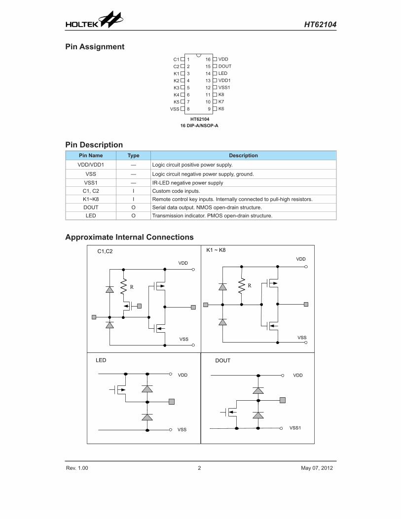
Pin Assignment� �� �� �� �� �� �� ��
��������
� �� �� �� �� �� �� �
� � �
� � �� � � � � �� � � �� � � �� �� �� �
� � � � � � �� � � � � � � � � � � � � � �
Pin DescriptionPin Name Type Description
VDD/VDD1 — Logic circuit positive power supply.
VSS — Logic circuit negative power supply, ground.
VSS1 — IR-LED negative power supplyC1, C2 I Custom code inputs.K1~K8 I Remote control key inputs. Internally connected to pull-high resistors.DOUT O Serial data output. NMOS open-drain structure.LED O Transmission indicator. PMOS open-drain structure.
Approximate Internal ConnectionsC1,C2 K1 ~ K8
LED
VSS
VDD
VSS1
DOUT
VSS
VDD
RR
VDD
VSS
VDD
Rev. 1.00 3 May 07, 2012
HT62104
Absolute Maximum RatingsSupplyVoltage…………………VSS-0.3VtoVSS+6.5VInputVoltage……………………VSS-0.3VtoVDD+0.3VOutputVoltage…………………VSS-0.3VtoVDD+0.3V
StorageTemperature…………………-55°Cto150°COperatingTemperature………………-10°Cto70°C
Note:Thesearestressratingsonly.Stressesexceedingtherangespecifiedunder“AbsoluteMaximumRatings”maycausesubstantialdamagetothedevice.Functionaloperationofthisdeviceatotherconditionsbeyondthoselistedin thespecificationisnot impliedandprolongedexposuretoextremeconditionsmayaffectdevicereliability.
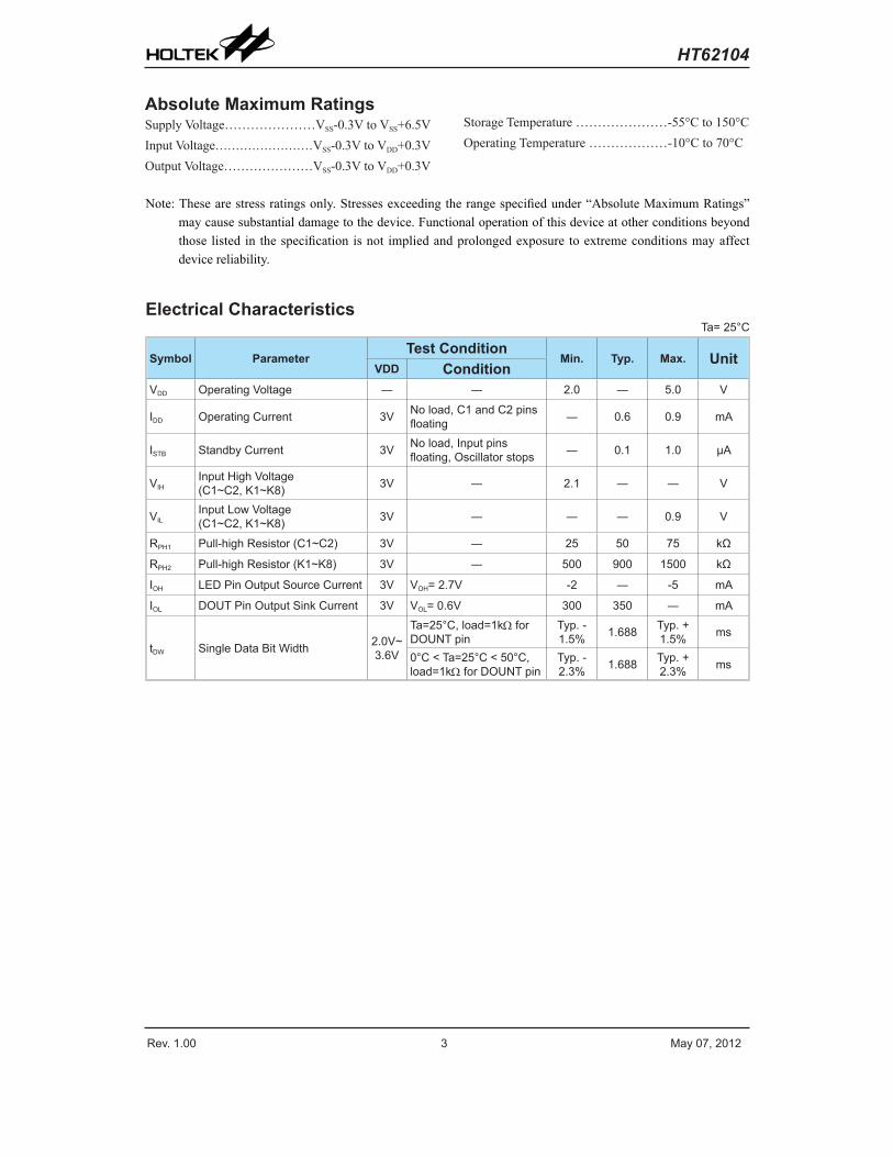
Electrical CharacteristicsTa= 25°C
Symbol ParameterTest Condition
Min. Typ. Max. UnitVDD Condition
VDD Operating Voltage ― ― 2.0 ― 5.0 V
IDD Operating Current 3V No load, C1 and C2 pins floating ― 0.6 0.9 mA
ISTB Standby Current 3V No load, Input pins floating, Oscillator stops ― 0.1 1.0 μA
VIHInput High Voltage(C1~C2, K1~K8) 3V ― 2.1 ― ― V
VILInput Low Voltage(C1~C2, K1~K8) 3V ― ― ― 0.9 V
RPH1 Pull-high Resistor (C1~C2) 3V ― 25 50 75 kΩ
RPH2 Pull-high Resistor (K1~K8) 3V ― 500 900 1500 kΩ
IOH LED Pin Output Source Current 3V VOH= 2.7V -2 ― -5 mA
IOL DOUT Pin Output Sink Current 3V VOL= 0.6V 300 350 ― mA
tDW Single Data Bit Width 2.0V~ 3.6V
Ta=25°C, load=1kW for DOUNT pin
Typ. - 1.5% 1.688 Typ. +
1.5% ms
0°C < Ta=25°C < 50°C, load=1kW for DOUNT pin
Typ. - 2.3% 1.688 Typ. +
2.3% ms
Rev. 1.00 4 May 07, 2012
HT62104
Functional DescriptionTheHT62104Infraredremotecontrolencoderpro-videsameansforeasyremotecontrolsignalencod-ing.Asallfunctions, includingthesystemoscillator,areintegratedwithinthedevice,theadditionofexter-nalswitchesandanIRLEDisall thatisrequiredtoimplementafullInfraredremotecontrol transmitterfunction.
Thedevicewillgenerateanencodedsignalonitsout-putpin,DOUT,composedofaStartcode,aCustomcodeandaDatacode.Thesignal isautomaticallygeneratedontheDOUTpinwhenanydatainputpin,K1~K8,changesstatefromhightolow.Theinternalpull-high resistorskeep thesedata inputpins inanormallyhighcondition.Theoutputsignalon theDOUTpincanbeinterfacedtoanexternalIRLEDforwirelesssignaltransmission.
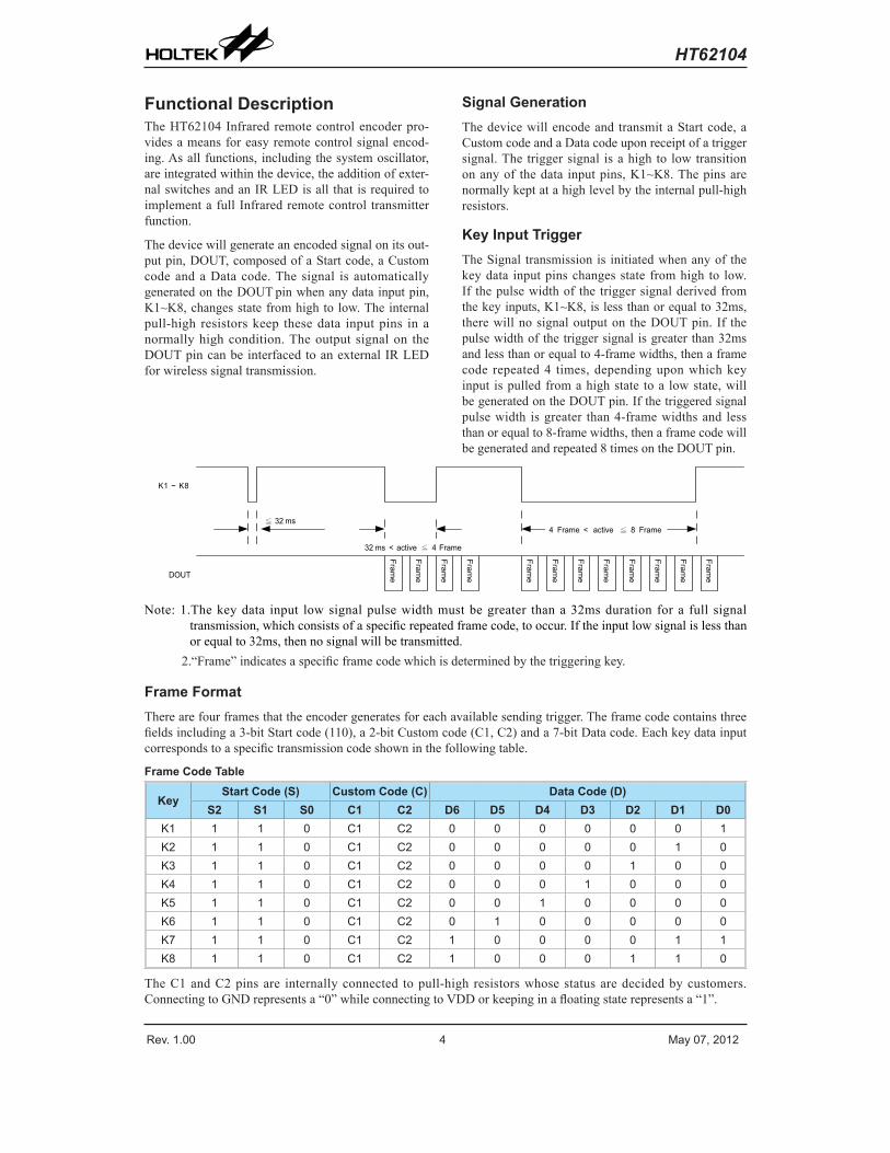
Signal GenerationThedevicewillencodeandtransmitaStartcode,aCustomcodeandaDatacodeuponreceiptofatriggersignal.Thetriggersignal isahighto lowtransitiononanyof thedata inputpins,K1~K8.Thepinsarenormallykeptatahighlevelbytheinternalpull-highresistors.
Key Input TriggerTheSignal transmissionis initiatedwhenanyof thekeydata inputpinschangesstate fromhigh to low.If thepulsewidthof the triggersignalderivedfromthekeyinputs,K1~K8,islessthanorequalto32ms,therewillnosignaloutputon theDOUTpin. If thepulsewidthofthetriggersignalisgreaterthan32msandlessthanorequalto4-framewidths,thenaframecode repeated4 times,dependinguponwhichkeyinput ispulledfromahighstate toa lowstate,willbegeneratedontheDOUTpin.Ifthetriggeredsignalpulsewidth isgreater than4-framewidthsand lessthanorequalto8-framewidths,thenaframecodewillbegeneratedandrepeated8timesontheDOUTpin.
K1 ~ K8
DOUT
32 ms
32 ms < active 4 Frame
4 Frame < active 8 Frame
Frame
Frame
Frame
Frame
Frame
Frame
Frame
Frame
Frame
Frame
Frame
Frame
Note:1.Thekeydata input lowsignalpulsewidthmustbegreater thana32msduration fora full signaltransmission,whichconsistsofaspecificrepeatedframecode,tooccur.Iftheinputlowsignalislessthanorequalto32ms,thennosignalwillbetransmitted.
2.“Frame”indicatesaspecificframecodewhichisdeterminedbythetriggeringkey.
Frame FormatTherearefourframesthattheencodergeneratesforeachavailablesendingtrigger.Theframecodecontainsthreefieldsincludinga3-bitStartcode(110),a2-bitCustomcode(C1,C2)anda7-bitDatacode.Eachkeydatainputcorrespondstoaspecifictransmissioncodeshowninthefollowingtable.
Frame Code Table
KeyStart Code (S) Custom Code (C) Data Code (D)
S2 S1 S0 C1 C2 D6 D5 D4 D3 D2 D1 D0K1 1 1 0 C1 C2 0 0 0 0 0 0 1K2 1 1 0 C1 C2 0 0 0 0 0 1 0K3 1 1 0 C1 C2 0 0 0 0 1 0 0K4 1 1 0 C1 C2 0 0 0 1 0 0 0K5 1 1 0 C1 C2 0 0 1 0 0 0 0K6 1 1 0 C1 C2 0 1 0 0 0 0 0K7 1 1 0 C1 C2 1 0 0 0 0 1 1K8 1 1 0 C1 C2 1 0 0 0 1 1 0
TheC1andC2pinsare internallyconnected topull-highresistorswhosestatusaredecidedbycustomers.ConnectingtoGNDrepresentsa“0”whileconnectingtoVDDorkeepinginafloatingstaterepresentsa“1”.
Rev. 1.00 5 May 07, 2012
HT62104
Frame Data Format On DOUT Pin• AoneFramedataformatisshownbelow.
S 2 S 1 S 0 C 1 C 2 D 6 D 5 D 4 D 3 D 2 D 1 D 0
Delay time ( 32 ms )
One frame ( 12 bits )
Start code Custom code Data code
Press key
DOUT
• ThetimedurationbetweenFrame(n)andFrame(n+1)iscalledtheSignalGapTime.TheGapTimeiscountedbasedonaunitperiod,denotedas“T”.
kHz4551
19244T1 ××=λ= ≈ kHz381
164 × ×
– FortheHT62104device,theSignalGapTimeis4T.
Delay time (32ms) Frame 1 4T Frame 2
Press key
Frame 3 4T Frame 44T
Release key
DOUT S C D S C D S C D S C D
Gap Time Gap Time Gap Time
Carrier Output WaveformThecarriersignal,witha frequencyof38kHz, issuperimposedonto theoutputdatasignalwhich isused togenerateanddata0anddata1waveforms.Thecarriersignalisshowninthefollowingdiagram.
26 .3µs
8.77 µs
38 KHz carrier
DOUT Pin Bit Code WaveformsAsbitscanbedesignatedaseither“0”or“1”,theymustbeencodedinacertainwayasshownbelow.
λ
Bit “0”
Bit “1”
tDW
38 kHz
3 λ
λ3 λ
Note:1.kHz455
11921 ×=λ ≈
kHz381
16 ×
2.Bit“1”consistsofa“high”pulsefor1λanda“38kHzcarrier”for3λ.
3.Bit“0”consistsofa“high”pulsefor3λanda“38kHzcarrier”for1λ.
Rev. 1.00 6 May 07, 2012
HT62104
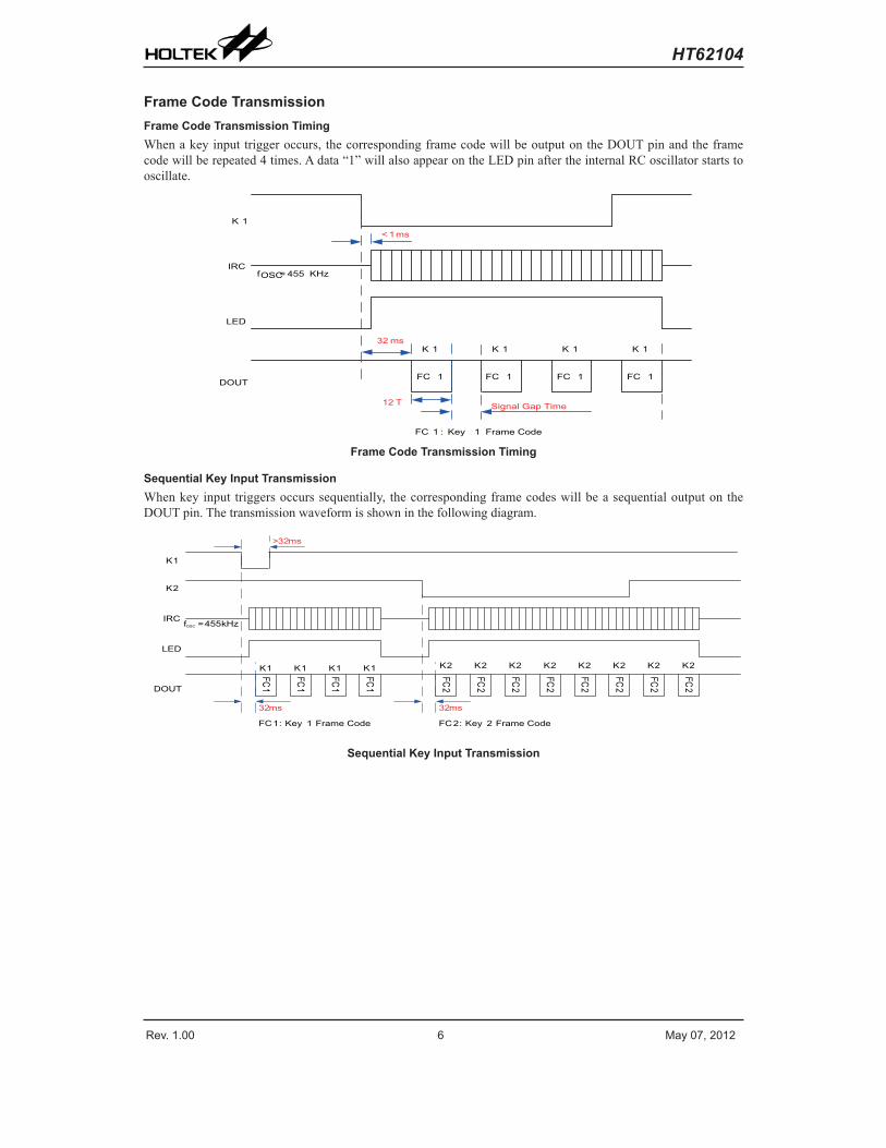
Frame Code TransmissionFrame Code Transmission TimingWhenakeyinputtriggeroccurs, thecorrespondingframecodewillbeoutputontheDOUTpinandtheframecodewillberepeated4times.Adata“1”willalsoappearontheLEDpinaftertheinternalRCoscillatorstartstooscillate.
K 1
IRC
LED
DOUTFC 1 FC 1 FC 1 FC 1
K 1 K 1 K 1 K 1
fOSC= 455 KHz
< 1ms
32 ms
12 T Signal Gap Time
FC 1 : Key 1 Frame Code
Frame Code Transmission Timing
Sequential Key Input TransmissionWhenkeyinputtriggersoccurssequentially, thecorrespondingframecodeswillbeasequentialoutputontheDOUTpin.Thetransmissionwaveformisshowninthefollowingdiagram.
K1
K2
IRC
LED
DOUT
K1 K1 K1 K1 K2 K2 K2 K2
fOSC =455kHz
>32ms
K2 K2 K2 K2
32ms 32ms
FC1
FC1
FC1
FC1
FC2
FC2
FC2
FC2
FC2
FC2
FC2
FC2
FC1: Key 1 Frame Code FC2: Key 2 Frame Code
Sequential Key Input Transmission

Rev. 1.00 7 May 07, 2012
HT62104
Overlapped Key Input TransmissionWhentwokeyinputtriggerpulsesoverlap,thetimewherethesecondtriggerpulseoccurswilldeterminewhatframecodewillbeoutputontheDOUTpin.Ifthesecondtriggerpulseoccursduringthegaptime,thefollowingframecodewillbeoutputontheDOUTpinandwillbeacombinationof thetwotriggeredframecodes.Thefollowingdiagramshowsthetransmissionwaveform.
K1
K2
IRC
LED
DOUT
K1+K2 K1+K2 K1+K2K1 K1 K2 K2 K2
fOSC = 455 kHz
FC1
FC1
FC2
FC2
FC2
FC1 + FC2
FC1 + FC2
FC1 + FC2
Gap Time
FC 1: Key 1 Frame Code.FC 2: Key 2 Frame Code.
FC 1+FC 2: Combination of Key 1 and Key 2 Frame Codes .
Overlapping Key Inputs Occurring During the Gap Time
Ifthesecondavailabletriggerpulseoccursduringtheframecodetransmissionduration,thepresentframecodebeingtransmittedwillstillbeoutputontheDOUTpin.Herethecombinationofthetwotriggeredframecodeswillbeconsecutivelyoutput.Thefollowingdiagramindicatesthetransmissionwaveform.
K1
K2
IRC
LED
DOUT
K1+K2 K1+K2K1 K1 K2 K2
fOSC = 455 kHz
FC1
FC1
FC2
FC2
FC1 + FC2
FC1 + FC2
Gap Time
FC 1: Key 1 Frame Code.FC 2: Key 2 Frame Code.
FC 1+FC 2: Combination of Key 1 and Key 2 Frame Codes.
K1
FC1
K1+K2
FC1 + FC2
Overlapping Key Inputs Occurring During a Frame Code Transmission
Thesamemethodologycanbeappliedontherisingtransitionofanyavailabletriggerpulsestoseehowtheframecodechangeswhenoverlappingkeyinputsoccur.
Rev. 1.00 8 May 07, 2012
HT62104
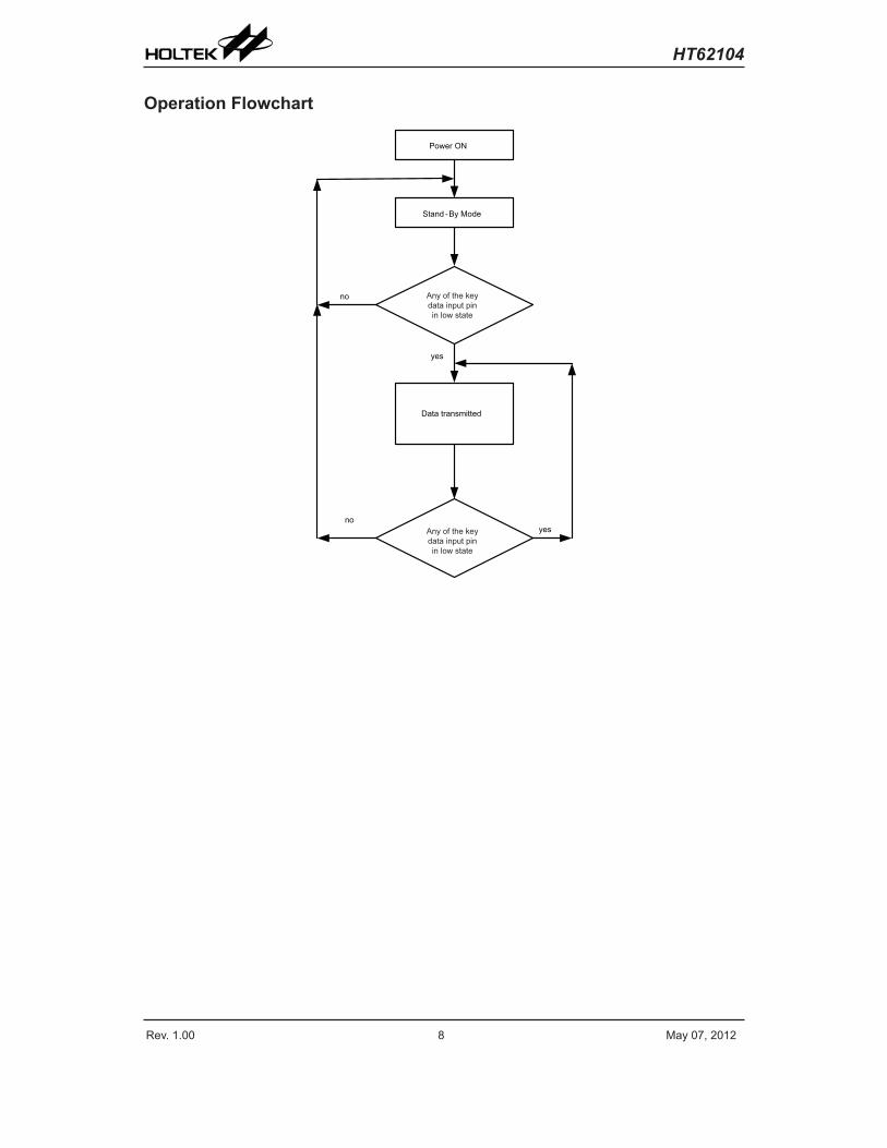
Operation Flowchart
Power ON
Stand -By Mode
Data transmitted
yes
no
yesno
Any of the keydata input pinin low state
Any of the keydata input pinin low state

Rev. 1.00 9 May 07, 2012
HT62104
Application Circuit
VDD
DOUT
LED
VDD1
VSS1
K8
K7
K6VSS
K5
K4
K3
K2
K1
C1
C2
1
2
3
4
5
6
7
8 9
10
11
12
13
14
15
16
K1
K2
K3
K4
K5
C1
C2
K8
K7
K6
1W IR LE
D
IR333C
-A(Q
)
HT62104
R1
VSS
LED
VSS1
VSS2Single-point
connection for GND
Single-point connection for VDD
R2 10W
220mFC1
VDD
V DD1
0.1mFC2
3V
Figure 1 (See Note)
VDD
DOUT
LED
VDD1
VSS1
K8
K7
K6VSS
K5
K4
K3
K2
K1
C1
C2K1
K2
K3
K4
K5
K6
K7
K8
3V 330mF
LED
1
2
3
4
5
6
7
8 9
10
11
12
13
14
15
16C1
C2
1mF
1W
IR LED
HT62104
IR333C-A(Q)
Figure 2
Note:1.VDD1providespowerfor theIR_LED;VDDprovidespowerfor theIC logiccircuits.The twopowersupplies,theC1(220mF)positiveterminalandthepositiveterminalofthebatterymusthaveasingle-pointconnection.
2.Before theVDDpowersupply isconnected to theICVDDpin,acapacitorC2(0.1mF)must firstbeconnectedclosetotheIC.
3.VSS1isGNDfortheDOUTdriver;VSS2isGNDfortheLEDdriver;VSSisGNDfortheIClogiccircuits.ThethreeGNDs,thenegativeterminalofC1(220mF)andthenegativeterminalofthebatterymusthaveasingle-pointconnection.
4.IfhighcurrentdriveconditionsforIR_LEDresultininstabilityonVDD(noise),itisrecommendtoaddaresistorR2tostabiliseVDDandVDD1pins.
5.TheDOUTandKEYtracksshouldbekeptapartbyadistanceof30milormore.6.DuringPCBmanufacture, theDOUT,VDD,VSS,VSS1,andVSS2tracksshouldnotbymadeusingcarbontracks.
Rev. 1.00 10 May 07, 2012
HT62104
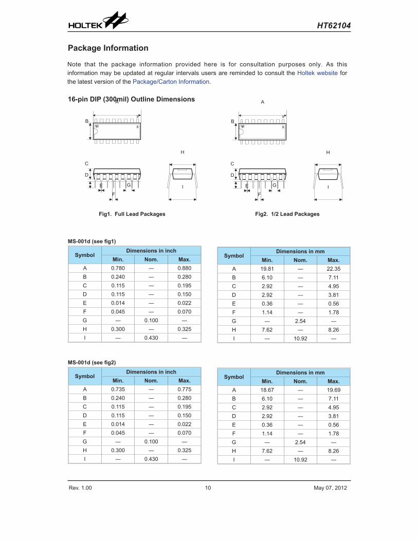
Package Information
16-pin DIP (300mil) Outline Dimensions
� �� ��
�
�
�
�
�
�
�
�
�
�
�
� �� ��
�
�
�
�
�
�
�
�
�
�
�
Fig1. Full Lead Packages Fig2. 1/2 Lead Packages
MS-001d (see fig1)
SymbolDimensions in inch
Min. Nom. Max.A 0.780 ― 0.880B 0.240 ― 0.280C 0.115 ― 0.195D 0.115 ― 0.150E 0.014 ― 0.022F 0.045 ― 0.070G ― 0.100 ―H 0.300 ― 0.325I ― 0.430 ―
SymbolDimensions in mm
Min. Nom. Max.A 19.81 ― 22.35B 6.10 ― 7.11C 2.92 ― 4.95D 2.92 ― 3.81E 0.36 ― 0.56F 1.14 ― 1.78G ― 2.54 ―H 7.62 ― 8.26I ― 10.92 ―
MS-001d (see fig2)
SymbolDimensions in inch
Min. Nom. Max.A 0.735 ― 0.775B 0.240 ― 0.280C 0.115 ― 0.195D 0.115 ― 0.150E 0.014 ― 0.022F 0.045 ― 0.070G ― 0.100 ―H 0.300 ― 0.325I ― 0.430 ―
SymbolDimensions in mm
Min. Nom. Max.A 18.67 ― 19.69B 6.10 ― 7.11C 2.92 ― 4.95D 2.92 ― 3.81E 0.36 ― 0.56F 1.14 ― 1.78G ― 2.54 ―H 7.62 ― 8.26I ― 10.92 ―
Note that the package information provided here is for consultation purposes only. As this information may be updated at regular intervals users are reminded to consult the Holtek website for the latest version of the Package/Carton Information.
Rev. 1.00 11 May 07, 2012
HT62104
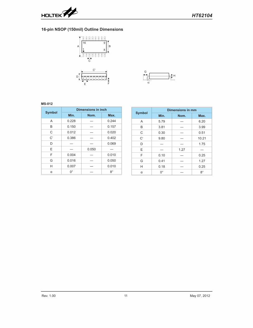
16-pin NSOP (150mil) Outline Dimensions
� �
�
�
�
�
� �
�
�
� �
��
� �
MS-012
SymbolDimensions in inch
Min. Nom. Max.A 0.228 ― 0.244
B 0.150 ― 0.157
C 0.012 ― 0.020
C’ 0.386 ― 0.402
D ― ― 0.069
E ― 0.050 ―
F 0.004 ― 0.010
G 0.016 ― 0.050
H 0.007 ― 0.010
α 0° ― 8°
SymbolDimensions in mm
Min. Nom. Max.A 5.79 ― 6.20
B 3.81 ― 3.99
C 0.30 ― 0.51
C‘ 9.80 ― 10.21
D ― ― 1.75
E ― 1.27 ―
F 0.10 ― 0.25
G 0.41 ― 1.27
H 0.18 ― 0.25
α 0° ― 8°
Rev. 1.00 12 May 07, 2012
HT62104
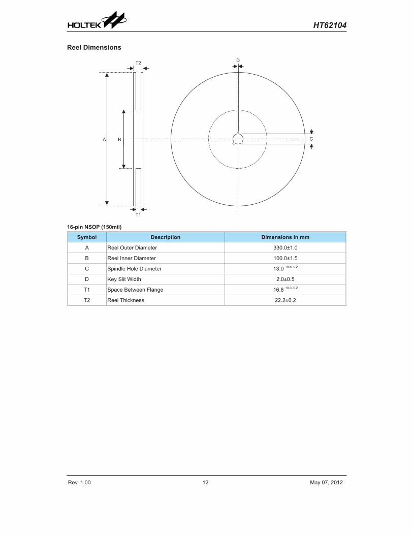
Reel Dimensions
� ��
� �
� � �
16-pin NSOP (150mil)
Symbol Description Dimensions in mm
A Reel Outer Diameter 330.0±1.0
B Reel Inner Diameter 100.0±1.5
C Spindle Hole Diameter 13.0 +0.5/-0.2
D Key Slit Width 2.0±0.5
T1 Space Between Flange 16.8 +0.3/-0.2
T2 Reel Thickness 22.2±0.2
Rev. 1.00 13 May 07, 2012
HT62104
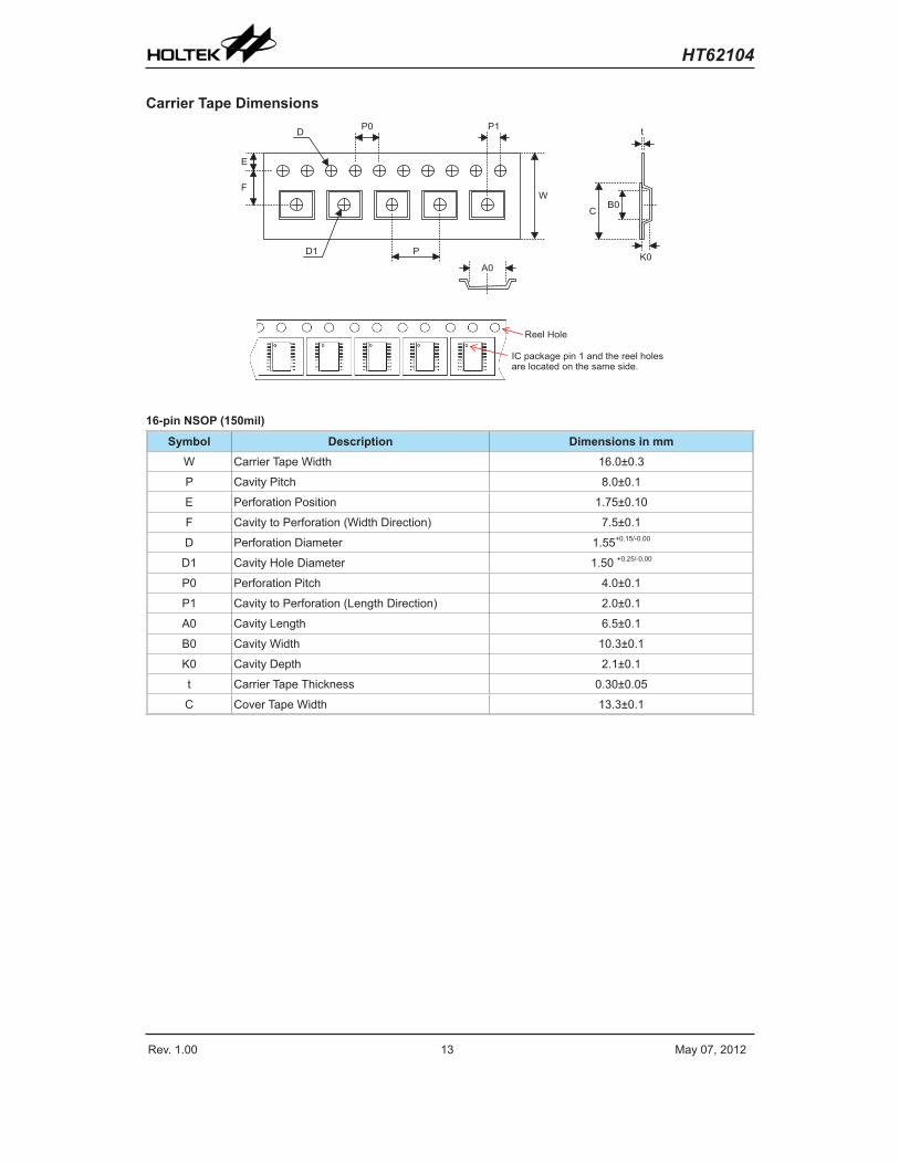
Carrier Tape Dimensions
�� �
�
� �� ��
�
�
�
� �
� �
� �
�
� � � � � � � � � � � � � � � � � � � � � � � � � � � � � � �� � � � � � � � � � � � � � � � � � � � � � � � � �
� � � � � � � � �
16-pin NSOP (150mil)
Symbol Description Dimensions in mm W Carrier Tape Width 16.0±0.3
P Cavity Pitch 8.0±0.1
E Perforation Position 1.75±0.10
F Cavity to Perforation (Width Direction) 7.5±0.1
D Perforation Diameter 1.55+0.15/-0.00
D1 Cavity Hole Diameter 1.50 +0.25/-0.00
P0 Perforation Pitch 4.0±0.1
P1 Cavity to Perforation (Length Direction) 2.0±0.1
A0 Cavity Length 6.5±0.1
B0 Cavity Width 10.3±0.1
K0 Cavity Depth 2.1±0.1
t Carrier Tape Thickness 0.30±0.05
C Cover Tape Width 13.3±0.1

Rev. 1.00 14 May 07, 2012
HT62104
Holtek Semiconductor Inc. (Headquarters)No.3, Creation Rd. II, Science Park, Hsinchu, TaiwanTel: 886-3-563-1999Fax: 886-3-563-1189http://www.holtek.com.tw
Holtek Semiconductor Inc. (Taipei Sales Office)4F-2, No. 3-2, YuanQu St., Nankang Software Park, Taipei 115, TaiwanTel: 886-2-2655-7070Fax: 886-2-2655-7373Fax: 886-2-2655-7383 (International sales hotline)
Holtek Semiconductor (China) Inc. (Dongguan Sales Office)Building No.10, Xinzhu Court, (No.1 Headquarters), 4 Cuizhu Road, Songshan Lake, Dongguan, China 523808Tel: 86-769-2626-1300Fax: 86-769-2626-1311, 86-769-2626-1322
Holtek Semiconductor (USA), Inc. (North America Sales Office)46729 Fremont Blvd., Fremont, CA 94538, USATel: 1-510-252-9880Fax: 1-510-252-9885http://www.holtek.com
Copyright© 2012 by HOLTEK SEMICONDUCTOR INC.The information appearing in this Data Sheet is believed to be accurate at the time of publication. However, Holtek assumes no responsibility arising from the use of the specifications described. The applications mentioned herein are used solely for the purpose of illustration and Holtek makes no warranty or representation that such applications will be suitable without further modification, nor recommends the use of its products for application that may present a risk to human life due to malfunction or otherwise. Holtek's products are not authorized for use as critical components in life support devices or systems. Holtek reserves the right to alter its products without prior notification. For the most up-to-date information, please visit our web site at http://www.holtek.com.tw.


![Personalized Multimedia Item and Key Frame Recommendation · with 80% of marketers use visual assets in the social media marketing[Stelzner, 2018]. As a key frame distills the visual](https://static.fdocuments.in/doc/165x107/5fb06e0680838f723924b1fe/personalized-multimedia-item-and-key-frame-recommendation-with-80-of-marketers.jpg)