HSPICE/SPICE™ Interface and SPICE™ 2G.6 Reference Manual
96
HSPICE/SPICE™ Interface and SPICE™ 2G.6 Reference Manual Product Version 5.1.41 June 2004
Transcript of HSPICE/SPICE™ Interface and SPICE™ 2G.6 Reference Manual

HSPICE/SPICE™ Interface and SPICE™2G.6 Reference Manual
Product Version 5.1.41June 2004

1999-2004 Cadence Design Systems, Inc. All rights reserved.Printed in the United States of America.
Cadence Design Systems, Inc., 555 River Oaks Parkway, San Jose, CA 95134, USA
Trademarks: Trademarks and service marks of Cadence Design Systems, Inc. (Cadence) contained inthis document are attributed to Cadence with the appropriate symbol. For queries regarding Cadence’strademarks, contact the corporate legal department at the address shown above or call 1-800-862-4522.
All other trademarks are the property of their respective holders.
Restricted Print Permission: This publication is protected by copyright and any unauthorized use of thispublication may violate copyright, trademark, and other laws. Except as specified in this permissionstatement, this publication may not be copied, reproduced, modified, published, uploaded, posted,transmitted, or distributed in any way, without prior written permission from Cadence. This statement grantsyou permission to print one (1) hard copy of this publication subject to the following conditions:
1. The publication may be used solely for personal, informational, and noncommercial purposes;2. The publication may not be modified in any way;3. Any copy of the publication or portion thereof must include all original copyright, trademark, and other
proprietary notices and this permission statement; and4. Cadence reserves the right to revoke this authorization at any time, and any such use shall be
discontinued immediately upon written notice from Cadence.
Disclaimer: Information in this publication is subject to change without notice and does not represent acommitment on the part of Cadence. The information contained herein is the proprietary and confidentialinformation of Cadence or its licensors, and is supplied subject to, and may be used only by Cadence’scustomer in accordance with, a written agreement between Cadence and its customer. Except as may beexplicitly set forth in such agreement, Cadence does not make, and expressly disclaims, anyrepresentations or warranties as to the completeness, accuracy or usefulness of the information containedin this document. Cadence does not warrant that use of such information will not infringe any third partyrights, nor does Cadence assume any liability for damages or costs of any kind that may result from use ofsuch information.
Restricted Rights: Use, duplication, or disclosure by the Government is subject to restrictions as set forthin FAR52.227-14 and DFAR252.227-7013 et seq. or its successor.

HSPICE/SPICE Interface and SPICE 2G.6 Reference Manual
Contents
Preface . . . . . . . . . . . . . . . . . . . . . . . . . . . . . . . . . . . . . . . . . . . . . . . . . . . . . . . . . . . . . . 7
About This Manual . . . . . . . . . . . . . . . . . . . . . . . . . . . . . . . . . . . . . . . . . . . . . . . . . . . . . . 7What You Need To Know First . . . . . . . . . . . . . . . . . . . . . . . . . . . . . . . . . . . . . . . . . . . 7Finding Information in This Manual . . . . . . . . . . . . . . . . . . . . . . . . . . . . . . . . . . . . . . . 7Using FrameMaker to Get Help . . . . . . . . . . . . . . . . . . . . . . . . . . . . . . . . . . . . . . . . . . 8
1Introduction . . . . . . . . . . . . . . . . . . . . . . . . . . . . . . . . . . . . . . . . . . . . . . . . . . . . . . . . . 9
Product Overview . . . . . . . . . . . . . . . . . . . . . . . . . . . . . . . . . . . . . . . . . . . . . . . . . . . . . . . 9SPICE . . . . . . . . . . . . . . . . . . . . . . . . . . . . . . . . . . . . . . . . . . . . . . . . . . . . . . . . . . . . . . 9HSPICE . . . . . . . . . . . . . . . . . . . . . . . . . . . . . . . . . . . . . . . . . . . . . . . . . . . . . . . . . . . . 9
Simulation Flow . . . . . . . . . . . . . . . . . . . . . . . . . . . . . . . . . . . . . . . . . . . . . . . . . . . . . . . . 10
2SPICE Circuit Simulation Interface . . . . . . . . . . . . . . . . . . . . . . . . . . . . . 11
Overview . . . . . . . . . . . . . . . . . . . . . . . . . . . . . . . . . . . . . . . . . . . . . . . . . . . . . . . . . . . . . 11Example of a SPICE Simulation Run . . . . . . . . . . . . . . . . . . . . . . . . . . . . . . . . . . . . . . . . 11
control file . . . . . . . . . . . . . . . . . . . . . . . . . . . . . . . . . . . . . . . . . . . . . . . . . . . . . . . . . . 12 netlist file . . . . . . . . . . . . . . . . . . . . . . . . . . . . . . . . . . . . . . . . . . . . . . . . . . . . . . . . . . 13 spice.inp file . . . . . . . . . . . . . . . . . . . . . . . . . . . . . . . . . . . . . . . . . . . . . . . . . . . . . . . . 13 spice.sim file . . . . . . . . . . . . . . . . . . . . . . . . . . . . . . . . . . . . . . . . . . . . . . . . . . . . . . . 13 si.inp file: Used as Input to SPICE . . . . . . . . . . . . . . . . . . . . . . . . . . . . . . . . . . . . . . 13si.log file: Produced from the Simulation Run . . . . . . . . . . . . . . . . . . . . . . . . . . . . . 14si.out file: Output of a SPICE Simulation Run . . . . . . . . . . . . . . . . . . . . . . . . . . . . . 14
3HSPICE Circuit Simulation Interface . . . . . . . . . . . . . . . . . . . . . . . . . . . 19
Overview . . . . . . . . . . . . . . . . . . . . . . . . . . . . . . . . . . . . . . . . . . . . . . . . . . . . . . . . . . . . . 19Running HSPICE . . . . . . . . . . . . . . . . . . . . . . . . . . . . . . . . . . . . . . . . . . . . . . . . . . . . . . . 20
Creating the Schematic . . . . . . . . . . . . . . . . . . . . . . . . . . . . . . . . . . . . . . . . . . . . . . . 20
June 2004 3 Product Version 5.1.41

HSPICE/SPICE Interface and SPICE 2G.6 Reference Manual
Generating the Run Directory . . . . . . . . . . . . . . . . . . . . . . . . . . . . . . . . . . . . . . . . . . . 21Editing the control File . . . . . . . . . . . . . . . . . . . . . . . . . . . . . . . . . . . . . . . . . . . . . . . . 21Starting the Analysis Run . . . . . . . . . . . . . . . . . . . . . . . . . . . . . . . . . . . . . . . . . . . . . . 21Generating the Netlist . . . . . . . . . . . . . . . . . . . . . . . . . . . . . . . . . . . . . . . . . . . . . . . . . 21Creating the Input File . . . . . . . . . . . . . . . . . . . . . . . . . . . . . . . . . . . . . . . . . . . . . . . . 21Running the Simulation . . . . . . . . . . . . . . . . . . . . . . . . . . . . . . . . . . . . . . . . . . . . . . . 22Translating the Output . . . . . . . . . . . . . . . . . . . . . . . . . . . . . . . . . . . . . . . . . . . . . . . . 22Viewing the Results . . . . . . . . . . . . . . . . . . . . . . . . . . . . . . . . . . . . . . . . . . . . . . . . . . 22
Hierarchical Netlisting . . . . . . . . . . . . . . . . . . . . . . . . . . . . . . . . . . . . . . . . . . . . . . . . . . . 22Primitive Cell Requirements . . . . . . . . . . . . . . . . . . . . . . . . . . . . . . . . . . . . . . . . . . . . 23Example . . . . . . . . . . . . . . . . . . . . . . . . . . . . . . . . . . . . . . . . . . . . . . . . . . . . . . . . . . . 24
4HSPICE/SPICE Elements . . . . . . . . . . . . . . . . . . . . . . . . . . . . . . . . . . . . . . . 25
Overview . . . . . . . . . . . . . . . . . . . . . . . . . . . . . . . . . . . . . . . . . . . . . . . . . . . . . . . . . . . . . 25HSPICE/SPICE Elements and Corresponding Library Cells . . . . . . . . . . . . . . . . . . . . 26HSPICE/SPICE Model and Element Parameters . . . . . . . . . . . . . . . . . . . . . . . . . . . . . . 27
Resistor . . . . . . . . . . . . . . . . . . . . . . . . . . . . . . . . . . . . . . . . . . . . . . . . . . . . . . . . . . . 27Capacitor . . . . . . . . . . . . . . . . . . . . . . . . . . . . . . . . . . . . . . . . . . . . . . . . . . . . . . . . . . 28Inductor . . . . . . . . . . . . . . . . . . . . . . . . . . . . . . . . . . . . . . . . . . . . . . . . . . . . . . . . . . . 28Transmission Line . . . . . . . . . . . . . . . . . . . . . . . . . . . . . . . . . . . . . . . . . . . . . . . . . . . . 29Diode . . . . . . . . . . . . . . . . . . . . . . . . . . . . . . . . . . . . . . . . . . . . . . . . . . . . . . . . . . . . . 30BJT . . . . . . . . . . . . . . . . . . . . . . . . . . . . . . . . . . . . . . . . . . . . . . . . . . . . . . . . . . . . . . . 31JFET . . . . . . . . . . . . . . . . . . . . . . . . . . . . . . . . . . . . . . . . . . . . . . . . . . . . . . . . . . . . . . 33MOSFET . . . . . . . . . . . . . . . . . . . . . . . . . . . . . . . . . . . . . . . . . . . . . . . . . . . . . . . . . . 34
Formatting Functions . . . . . . . . . . . . . . . . . . . . . . . . . . . . . . . . . . . . . . . . . . . . . . . . . . . . 36 Element Formats . . . . . . . . . . . . . . . . . . . . . . . . . . . . . . . . . . . . . . . . . . . . . . . . . . . . 37Model Format . . . . . . . . . . . . . . . . . . . . . . . . . . . . . . . . . . . . . . . . . . . . . . . . . . . . . . . 39
5Using SPICE . . . . . . . . . . . . . . . . . . . . . . . . . . . . . . . . . . . . . . . . . . . . . . . . . . . . . . 41
Introduction . . . . . . . . . . . . . . . . . . . . . . . . . . . . . . . . . . . . . . . . . . . . . . . . . . . . . . . . . . . 42Types of Analysis . . . . . . . . . . . . . . . . . . . . . . . . . . . . . . . . . . . . . . . . . . . . . . . . . . . . . . . 42
DC Analysis . . . . . . . . . . . . . . . . . . . . . . . . . . . . . . . . . . . . . . . . . . . . . . . . . . . . . . . . 42AC Small-Signal Analysis . . . . . . . . . . . . . . . . . . . . . . . . . . . . . . . . . . . . . . . . . . . . . . 43
June 2004 4 Product Version 5.1.41

HSPICE/SPICE Interface and SPICE 2G.6 Reference Manual
Transient Analysis . . . . . . . . . . . . . . . . . . . . . . . . . . . . . . . . . . . . . . . . . . . . . . . . . . . . 43Analysis at Different Temperatures . . . . . . . . . . . . . . . . . . . . . . . . . . . . . . . . . . . . . . . 44
Convergence . . . . . . . . . . . . . . . . . . . . . . . . . . . . . . . . . . . . . . . . . . . . . . . . . . . . . . . . . . 45Input Format . . . . . . . . . . . . . . . . . . . . . . . . . . . . . . . . . . . . . . . . . . . . . . . . . . . . . . . . . . 45Circuit Description . . . . . . . . . . . . . . . . . . . . . . . . . . . . . . . . . . . . . . . . . . . . . . . . . . . . . . 46Title Card, Comment Cards, and .END Card . . . . . . . . . . . . . . . . . . . . . . . . . . . . . . . . . . 47
Title Card . . . . . . . . . . . . . . . . . . . . . . . . . . . . . . . . . . . . . . . . . . . . . . . . . . . . . . . . . . 47.END Card . . . . . . . . . . . . . . . . . . . . . . . . . . . . . . . . . . . . . . . . . . . . . . . . . . . . . . . . . 47Comment Card . . . . . . . . . . . . . . . . . . . . . . . . . . . . . . . . . . . . . . . . . . . . . . . . . . . . . . 47
Element Cards for Passive Circuit Elements and Sources . . . . . . . . . . . . . . . . . . . . . . . 48Resistors . . . . . . . . . . . . . . . . . . . . . . . . . . . . . . . . . . . . . . . . . . . . . . . . . . . . . . . . . . 48Capacitors and Inductors . . . . . . . . . . . . . . . . . . . . . . . . . . . . . . . . . . . . . . . . . . . . . . 48Coupled (Mutual) Inductors . . . . . . . . . . . . . . . . . . . . . . . . . . . . . . . . . . . . . . . . . . . . 49Transmission Lines (Lossless) . . . . . . . . . . . . . . . . . . . . . . . . . . . . . . . . . . . . . . . . . . 49Linear Dependent Sources . . . . . . . . . . . . . . . . . . . . . . . . . . . . . . . . . . . . . . . . . . . . . 50Independent Sources . . . . . . . . . . . . . . . . . . . . . . . . . . . . . . . . . . . . . . . . . . . . . . . . . 52
Semiconductor Devices . . . . . . . . . . . . . . . . . . . . . . . . . . . . . . . . . . . . . . . . . . . . . . . . . . 56Element Cards for Semiconductor Devices . . . . . . . . . . . . . . . . . . . . . . . . . . . . . . . . . . . 56
Junction Diodes . . . . . . . . . . . . . . . . . . . . . . . . . . . . . . . . . . . . . . . . . . . . . . . . . . . . . 56Bipolar Junction Transistors (BJT) . . . . . . . . . . . . . . . . . . . . . . . . . . . . . . . . . . . . . . . 57Junction Field-Effect Transistors (JFET) . . . . . . . . . . . . . . . . . . . . . . . . . . . . . . . . . . . 57MOSFET . . . . . . . . . . . . . . . . . . . . . . . . . . . . . . . . . . . . . . . . . . . . . . . . . . . . . . . . . . 58
MODEL Cards for Semiconductor Devices . . . . . . . . . . . . . . . . . . . . . . . . . . . . . . . . . . . 59.MODEL Card . . . . . . . . . . . . . . . . . . . . . . . . . . . . . . . . . . . . . . . . . . . . . . . . . . . . . . . 59Diode Model Type . . . . . . . . . . . . . . . . . . . . . . . . . . . . . . . . . . . . . . . . . . . . . . . . . . . . 59NPN and PNP Model Type (BJT Model) . . . . . . . . . . . . . . . . . . . . . . . . . . . . . . . . . . 60NJF and PJF Model Type (JFET Model) . . . . . . . . . . . . . . . . . . . . . . . . . . . . . . . . . . 63NMOS & PMOS Model Type (MOSFET Model) . . . . . . . . . . . . . . . . . . . . . . . . . . . . . 64
Subcircuits . . . . . . . . . . . . . . . . . . . . . . . . . . . . . . . . . . . . . . . . . . . . . . . . . . . . . . . . . . . 68.SUBCKT Card . . . . . . . . . . . . . . . . . . . . . . . . . . . . . . . . . . . . . . . . . . . . . . . . . . . . . . 68.ENDS Card . . . . . . . . . . . . . . . . . . . . . . . . . . . . . . . . . . . . . . . . . . . . . . . . . . . . . . . . 69Subcircuit Calls . . . . . . . . . . . . . . . . . . . . . . . . . . . . . . . . . . . . . . . . . . . . . . . . . . . . . . 69
Control Cards . . . . . . . . . . . . . . . . . . . . . . . . . . . . . . . . . . . . . . . . . . . . . . . . . . . . . . . . . . 69.TEMP Card . . . . . . . . . . . . . . . . . . . . . . . . . . . . . . . . . . . . . . . . . . . . . . . . . . . . . . . . 69.WIDTH Card . . . . . . . . . . . . . . . . . . . . . . . . . . . . . . . . . . . . . . . . . . . . . . . . . . . . . . . 70.OPTIONS Card . . . . . . . . . . . . . . . . . . . . . . . . . . . . . . . . . . . . . . . . . . . . . . . . . . . . . 70
June 2004 5 Product Version 5.1.41

HSPICE/SPICE Interface and SPICE 2G.6 Reference Manual
.OP Card . . . . . . . . . . . . . . . . . . . . . . . . . . . . . . . . . . . . . . . . . . . . . . . . . . . . . . . . . . 72
.DC Card . . . . . . . . . . . . . . . . . . . . . . . . . . . . . . . . . . . . . . . . . . . . . . . . . . . . . . . . . . 73
.NODESET Card . . . . . . . . . . . . . . . . . . . . . . . . . . . . . . . . . . . . . . . . . . . . . . . . . . . . 73
.IC Card . . . . . . . . . . . . . . . . . . . . . . . . . . . . . . . . . . . . . . . . . . . . . . . . . . . . . . . . . . . 74
.TF Card . . . . . . . . . . . . . . . . . . . . . . . . . . . . . . . . . . . . . . . . . . . . . . . . . . . . . . . . . . . 74
.SENS Card . . . . . . . . . . . . . . . . . . . . . . . . . . . . . . . . . . . . . . . . . . . . . . . . . . . . . . . . 75
.AC Card . . . . . . . . . . . . . . . . . . . . . . . . . . . . . . . . . . . . . . . . . . . . . . . . . . . . . . . . . . . 75
.DISTO Card . . . . . . . . . . . . . . . . . . . . . . . . . . . . . . . . . . . . . . . . . . . . . . . . . . . . . . . . 75
.NOISE Card . . . . . . . . . . . . . . . . . . . . . . . . . . . . . . . . . . . . . . . . . . . . . . . . . . . . . . . 76
.TRAN Card . . . . . . . . . . . . . . . . . . . . . . . . . . . . . . . . . . . . . . . . . . . . . . . . . . . . . . . . 77
.FOUR Card . . . . . . . . . . . . . . . . . . . . . . . . . . . . . . . . . . . . . . . . . . . . . . . . . . . . . . . . 78
.PRINT Card . . . . . . . . . . . . . . . . . . . . . . . . . . . . . . . . . . . . . . . . . . . . . . . . . . . . . . . . 78
.PLOT Card . . . . . . . . . . . . . . . . . . . . . . . . . . . . . . . . . . . . . . . . . . . . . . . . . . . . . . . . 80Example of Data Decks . . . . . . . . . . . . . . . . . . . . . . . . . . . . . . . . . . . . . . . . . . . . . . . . . . 80
Circuit 1 . . . . . . . . . . . . . . . . . . . . . . . . . . . . . . . . . . . . . . . . . . . . . . . . . . . . . . . . . . . 80Circuit 2 . . . . . . . . . . . . . . . . . . . . . . . . . . . . . . . . . . . . . . . . . . . . . . . . . . . . . . . . . . . 81Circuit 3 . . . . . . . . . . . . . . . . . . . . . . . . . . . . . . . . . . . . . . . . . . . . . . . . . . . . . . . . . . . 81Circuit 4 . . . . . . . . . . . . . . . . . . . . . . . . . . . . . . . . . . . . . . . . . . . . . . . . . . . . . . . . . . . 82Circuit 5 . . . . . . . . . . . . . . . . . . . . . . . . . . . . . . . . . . . . . . . . . . . . . . . . . . . . . . . . . . . 83
Nonlinear Dependent Sources . . . . . . . . . . . . . . . . . . . . . . . . . . . . . . . . . . . . . . . . . . . . . 84Voltage-Controlled Current Sources . . . . . . . . . . . . . . . . . . . . . . . . . . . . . . . . . . . . . . 85Voltage-Controlled Voltage Sources . . . . . . . . . . . . . . . . . . . . . . . . . . . . . . . . . . . . . . 86Current-Controlled Current Sources . . . . . . . . . . . . . . . . . . . . . . . . . . . . . . . . . . . . . . 86Current-Controlled Voltage Sources . . . . . . . . . . . . . . . . . . . . . . . . . . . . . . . . . . . . . . 87
Bipolar Model Equations (Gmin terms omitted) . . . . . . . . . . . . . . . . . . . . . . . . . . . . . . . . 87DC Model . . . . . . . . . . . . . . . . . . . . . . . . . . . . . . . . . . . . . . . . . . . . . . . . . . . . . . . . . . 88AC Model . . . . . . . . . . . . . . . . . . . . . . . . . . . . . . . . . . . . . . . . . . . . . . . . . . . . . . . . . . 89Noise Model . . . . . . . . . . . . . . . . . . . . . . . . . . . . . . . . . . . . . . . . . . . . . . . . . . . . . . . . 91Temperature Effects . . . . . . . . . . . . . . . . . . . . . . . . . . . . . . . . . . . . . . . . . . . . . . . . . . 91Excess Phase . . . . . . . . . . . . . . . . . . . . . . . . . . . . . . . . . . . . . . . . . . . . . . . . . . . . . . . 92
Alter Statement and the Source-Stepping Method . . . . . . . . . . . . . . . . . . . . . . . . . . . . . 92References . . . . . . . . . . . . . . . . . . . . . . . . . . . . . . . . . . . . . . . . . . . . . . . . . . . . . . . . . . . . 93
Index. . . . . . . . . . . . . . . . . . . . . . . . . . . . . . . . . . . . . . . . . . . . . . . . . . . . . . . . . . . . . . . . 95
June 2004 6 Product Version 5.1.41
HSPICE/SPICE Interface and SPICE 2G.6 Reference Manual
Preface
About This Manual
This manual is for engineers and designers of integrated circuits. It is a reference to thefollowing products:
■ The HSPICE™ interface, which lets you run an HSPICE simulation in the Cadenceenvironment
■ The SPICE interface, which lets you run a SPICE simulation in the Cadence environment
■ The SPICE 2G.6 circuit simulator developed by the University of California at Berkeley
What You Need To Know First
Before you read this manual or use these simulations interfaces to run simulation, you shouldread
■ The Cadence Design Framework II User Guide for general information about gettingaround in the Cadence software. This manual shows you how to start the system, usethe mouse and windows, and start a design session.
■ The Simulation Environment Help for setting up and running a basic simulation usingmenus and forms
Finding Information in This Manual
The following table summarizes the topics covered in this manual.
For information about. . . Read . . .
Running a SPICE simulation Chapter 2, “SPICE Circuit Simulation Interface”
Running an HSPICE simulation Chapter 3, “HSPICE Circuit Simulation Interface”
sample library & simulationmodels
Chapter 4, “SPICE/HSPICE Simulation Models”
SPICE version 2G.6 Chapter 5, “Using SPICE ”
June 2004 7 Product Version 5.1.41
HSPICE/SPICE Interface and SPICE 2G.6 Reference ManualPreface
Using FrameMaker to Get Help
You can use FrameMaker to open the Online Reference Index directly. Clicking on a manualtitle in the Online Reference Index opens the Table of Contents for that manual. From theTable of Contents, you can go to specific pages in the manual. The arrows and buttons at thebottom of each page move you around in the document, return you to the Table of Contentsor the Online Reference Index, or quit the Online Reference system.
June 2004 8 Product Version 5.1.41

HSPICE/SPICE Interface and SPICE 2G.6 Reference Manual
1Introduction
This chapter includes the following topics:
■ Product Overview
■ Simulation Flow
Product Overview
SPICE
SPICE is a general-purpose circuit simulator developed by the University of California atBerkeley. It is used for nonlinear DC, nonlinear transient, and linear AC analysis. Cadencesupports a library of primitives and a full interface to SPICE version 2G.6. Cadence does notsell the SPICE program but supplies a copy of this public Domain program and its manualfree of charge when you purchase the interface.
HSPICE
HSPICE is a general-purpose circuit simulator from Meta-Software. It has an extensive set ofbuilt-in device models, including models for small geometry MOSFETs and MESFETs. Theprogram is compatible with SPICE and MSING input formats. Cadence supports a library ofprimitives and a full interface for HSPICE.
June 2004 9 Product Version 5.1.41
HSPICE/SPICE Interface and SPICE 2G.6 Reference ManualIntroduction
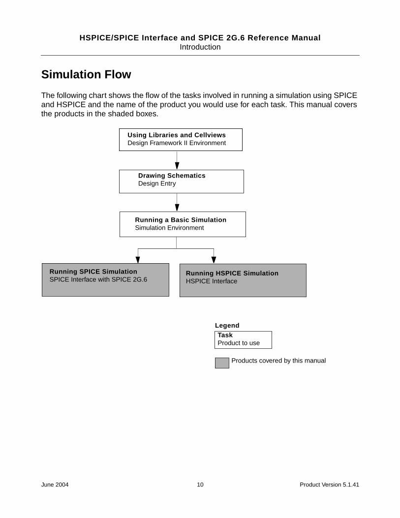
Simulation Flow
The following chart shows the flow of the tasks involved in running a simulation using SPICEand HSPICE and the name of the product you would use for each task. This manual coversthe products in the shaded boxes.
Running a Basic SimulationSimulation Environment
TaskProduct to use
Legend
Running HSPICE SimulationHSPICE Interface
Running SPICE SimulationSPICE Interface with SPICE 2G.6
Products covered by this manual
Drawing SchematicsDesign Entry
Using Libraries and CellviewsDesign Framework II Environment
June 2004 10 Product Version 5.1.41

HSPICE/SPICE Interface and SPICE 2G.6 Reference Manual
2SPICE Circuit Simulation Interface
This chapter contains the following topics:
■ Overview
■ Example of a SPICE Simulation Run
Overview
To set up and run a basic simulation using menus and forms, refer to SimulationEnvironment Help. Here is information specific to running the SPICE simulator:
■ SPICE does not have a command to read an input file, so the netlist file must bespecified in the control file with the simulation environment file inclusion function,“[!netlist]”; this tells the interface to include the netlist file in the file that is passed toSPICE. For an example of this, refer to the sample SPICE control file in "Example of aSPICE Simulation Run” on page 15. Any other command or stimulus files you want touse as input to SPICE can be specified in the same way.
■ The template control file for SPICE includes two other files in addition to the netlist file,spice.inp and spice.sim. These files are for stimulus data and simulator commands.The Initialize command from the Simulation menu automatically creates templates forthese files in a new run directory.
■ The waveform interface for SPICE does not handle multiple analysis simulation runs. Toview waveforms, perform one analysis for each simulation run.
■ The Waveform Display program does not display results of AC small-signal analysissimulation runs. Use the SPICE .PRINT or .PLOT commands to generate SPICE textoutput, and read it using the view output command.
Example of a SPICE Simulation Run
This section shows an example of input and output files needed for running a SPICEsimulation.
June 2004 11 Product Version 5.1.41

HSPICE/SPICE Interface and SPICE 2G.6 Reference ManualSPICE Circuit Simulation Interface
The following input and output files are for running the simulation on the inverter shown below:
■ The control file is used as an input for running the simulation.
■ The netlist file created by running the netlister on the design.
■ The si.inp file is created by the simulation interface and is passed to SPICE. This file isformed by including the specified files in the control file and mapping the user-definednames to numbers suitable for SPICE.
■ The spice.inp file is created by the Initialize command. Modify this file by adding thestimulus data.
■ The spice.sim file is created by the Initialize command. Modify this file by adding thesimulator commands.
■ The si.log file is the log of the simulation run.
■ The si.out file is the text output created by SPICE.
control file
* Spice control file
.options acct opts nopage limpts=1000
.width in=80 out=80[!spice.inp][!netlist][!spice.sim].end
p6u/2u
1
n4u/2u
0
OUTIN
2
1pf
June 2004 12 Product Version 5.1.41

HSPICE/SPICE Interface and SPICE 2G.6 Reference ManualSPICE Circuit Simulation Interface
netlist file
* net 1 = vdd!* net 0 = gnd!* net 2 = /OUT* net 3 = /IN.MODEL Model1 pmos level=2 vto=-.7 kp=1.5e-05 gamma=.4+lambda=.03 tox=6.e-07 xqc=.5* pmos(0) = /1M$#0 1 3 2 1 Model1 l=2u w=6u* capacitor(1) = /2C$#1 2 0 poly 1pf.MODEL Model3 nmos level=2 vto=.7 kp=3.e-05 gamma=.2 +lambda=.02+ tox=6.e-07 xqc=.5* nmos(2) = /0M$#2 2 3 0 0 Model3 l=2u w=4u
spice.inp file
vdd [#vdd!] [#gnd!] dc 5vvin [#/IN] 0 pwl 0 0 100ns 5v 150ns 5v 250ns 0
spice.sim file
.tran 1ns 300ns
si.inp file: Used as Input to SPICE
* Spice control file
.options acct opts nopage limpts=1000
.width in=80 out=80vdd 1 0 dc 5vvin 3 0 pwl 0 0 100ns 5v 150ns 5v 250ns 0* net 1 = vdd!* net 0 = gnd!* net 2 = /OUT* net 3 = /IN.MODEL Model1 pmos level=2 vto=-.7 kp=1.5e-05 gamma=.4+lambda=.03 tox=6.e-07 xqc=.5* pmos(0) = /1M$#0 1 3 2 1 Model1 l=2u w=6u* capacitor(1) = /2C$#1 2 0 poly 1pf.MODEL Model3 nmos level=2 vto=.7 kp=3.e-05 gamma=.2
June 2004 13 Product Version 5.1.41
HSPICE/SPICE Interface and SPICE 2G.6 Reference ManualSPICE Circuit Simulation Interface
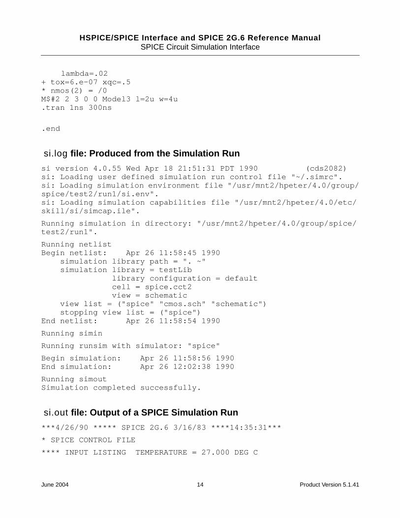
lambda=.02+ tox=6.e-07 xqc=.5* nmos(2) = /0M$#2 2 3 0 0 Model3 l=2u w=4u.tran 1ns 300ns
.end
si.log file: Produced from the Simulation Run
si version 4.0.55 Wed Apr 18 21:51:31 PDT 1990 (cds2082)si: Loading user defined simulation run control file "~/.simrc".si: Loading simulation environment file "/usr/mnt2/hpeter/4.0/group/spice/test2/run1/si.env".si: Loading simulation capabilities file "/usr/mnt2/hpeter/4.0/etc/skill/si/simcap.ile".
Running simulation in directory: "/usr/mnt2/hpeter/4.0/group/spice/test2/run1".
Running netlistBegin netlist: Apr 26 11:58:45 1990 simulation library path = ". ~" simulation library = testLib library configuration = default cell = spice.cct2 view = schematic view list = ("spice" "cmos.sch" "schematic") stopping view list = ("spice")End netlist: Apr 26 11:58:54 1990
Running simin
Running runsim with simulator: "spice"
Begin simulation: Apr 26 11:58:56 1990End simulation: Apr 26 12:02:38 1990
Running simoutSimulation completed successfully.
si.out file: Output of a SPICE Simulation Run
***4/26/90 ***** SPICE 2G.6 3/16/83 ****14:35:31***
* SPICE CONTROL FILE
**** INPUT LISTING TEMPERATURE = 27.000 DEG C
June 2004 14 Product Version 5.1.41

HSPICE/SPICE Interface and SPICE 2G.6 Reference ManualSPICE Circuit Simulation Interface
********************************************************.OPTIONS ACCT OPTS NOPAGE LIMPTS=1000.WIDTH IN=80 OUT=80VDD vdd! gnd! DC 5VVIN /IN gnd! PWL 0 0 100NS 5V 150NS 5V 250NS 0* NET 1 = VDD!* NET 0 = GND!* NET 2 = /OUT* NET 3 = /IN.MODEL MODEL1 PMOS LEVEL=2 VTO=-.7 KP=1.5E-05 GAMMA=.4+LAMBDA=.03 TOX=6 .E-07 XQC=.5* PMOS(0) = /1M/1 vdd! /IN /OUT vdd! MODEL1 L=2U W=6U* CAPACITOR(1) = /2C/2 /OUT gnd! POLY 1PF.MODEL MODEL3 NMOS LEVEL=2 VTO=.7 KP=3.E-05 GAMMA=.2+ LAMBDA=.02+ TOX=6.E-07 XQC=.5* NMOS(2) = /0M/0 /OUT /IN gnd! gnd! MODEL3 L=2U W=4U.TRAN 1NS 300NS.END******************************************************************** MOSFET MODEL PARAMETERS TEMPERATURE = 27.000 DEG C MODEL1 MODEL3TYPE PMOS NMOSLEVEL 2.000 2.000VTO -0.700 0.700KP 1.50D-05 3.00D-05GAMMA 0.400 0.200LAMBDA 3.00D-02 2.00D-02TOX 6.00D-07 6.00D-07XQC 0.500 0.500**** OPTION SUMMARY TEMPERATURE = 27.000 DEG CDC ANALYSIS -GMIN = 1.000D-12RELTOL = 1.000D-03ABSTOL = 1.000D-12VNTOL = 1.000D-06LVLCOD = 1ITL1 = 100ITL2 = 50PIVTOL = 1.000D-13PIVREL = 1.000D-03TRANSIENT ANALYSIS -METHOD = TRAP
June 2004 15 Product Version 5.1.41
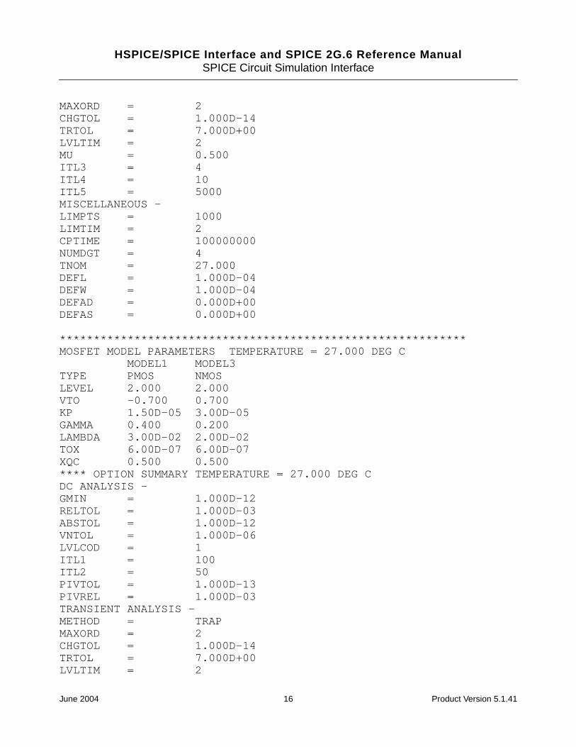
HSPICE/SPICE Interface and SPICE 2G.6 Reference ManualSPICE Circuit Simulation Interface
MAXORD = 2CHGTOL = 1.000D-14TRTOL = 7.000D+00LVLTIM = 2MU = 0.500ITL3 = 4ITL4 = 10ITL5 = 5000MISCELLANEOUS -LIMPTS = 1000LIMTIM = 2CPTIME = 100000000NUMDGT = 4TNOM = 27.000DEFL = 1.000D-04DEFW = 1.000D-04DEFAD = 0.000D+00DEFAS = 0.000D+00
************************************************************MOSFET MODEL PARAMETERS TEMPERATURE = 27.000 DEG C MODEL1 MODEL3TYPE PMOS NMOSLEVEL 2.000 2.000VTO -0.700 0.700KP 1.50D-05 3.00D-05GAMMA 0.400 0.200LAMBDA 3.00D-02 2.00D-02TOX 6.00D-07 6.00D-07XQC 0.500 0.500**** OPTION SUMMARY TEMPERATURE = 27.000 DEG CDC ANALYSIS -GMIN = 1.000D-12RELTOL = 1.000D-03ABSTOL = 1.000D-12VNTOL = 1.000D-06LVLCOD = 1ITL1 = 100ITL2 = 50PIVTOL = 1.000D-13PIVREL = 1.000D-03TRANSIENT ANALYSIS -METHOD = TRAPMAXORD = 2CHGTOL = 1.000D-14TRTOL = 7.000D+00LVLTIM = 2
June 2004 16 Product Version 5.1.41

HSPICE/SPICE Interface and SPICE 2G.6 Reference ManualSPICE Circuit Simulation Interface
MU = 0.500ITL3 = 4ITL4 = 10ITL5 = 5000MISCELLANEOUS -LIMPTS = 1000LIMTIM = 2CPTIME = 100000000NUMDGT = 4TNOM = 27.000DEFL = 1.000D-04DEFW = 1.000D-04DEFAD = 0.000D+00DEFAS = 0.000D+00********************************************************INITIAL TRANSIENT SOLUTION TEMPERATURE = 27.000 DEG CNODE VOLTAGE NODE VOLTAGE NODE VOLTAGE(vdd!) 5.0000 (/OUT) 5.0000 (/IN) 0.0000VOLTAGE SOURCE CURRENTSNAME CURRENTVDD -6.933D-12VIN 0.000D+00TOTAL POWER DISSIPATION 3.47D-11 WATTS********************************************************OPERATING POINT INFORMATION TEMPERATURE = 27.000 DEG C**** MOSFETS M/1 M/0MODEL MODEL1 MODEL3ID 6.80E-12 1.93E-12VGS -5.000 0.000VDS 0.000 5.000VBS 0.000 0.000JOB CONCLUDED**** JOB STATISTICS SUMMARY TEMPERATURE = 27.000 DEG CNUNODS NCNODS NUMNOD NUMEL DIODES BJTS JFETS MFETS4 4 4 5 0 0 0 2NUMTEM ICVFLG JTRFLG JACFLG INOISE IDIST NOGO1 0 301 0 0 0 0NSTOP NTTBR NTTAR IFILL IOPS PERSPA6. 13. 13. 0. 21. 63.889NUMTTP NUMRTP NUMNIT MAXMEM MEMUSE COPYKNT71. 4. 170. 249984 1576 15052.READIN 0.42SETUP 0.05TRCURV 0.00 0.DCAN 0.18 13.DCDCMP 0.067 2.
June 2004 17 Product Version 5.1.41

HSPICE/SPICE Interface and SPICE 2G.6 Reference ManualSPICE Circuit Simulation Interface
DCSOL 0.067ACAN 0.00 0.TRANAN 3.63 170.OUTPUT 0.00LOAD 3.067CODGEN 0.000 1fs 0.CODEXC 0.000MACINS 0.000OVERHEAD 0.07TOTAL JOB TIME 4.35********************************************************
June 2004 18 Product Version 5.1.41

HSPICE/SPICE Interface and SPICE 2G.6 Reference Manual
3HSPICE Circuit Simulation Interface
This chapter contains the following topics:
■ Overview
■ Running HSPICE
■ Hierarchical Netlisting
Overview
Using the HSPICE interface is very similar to using the SPICE interface. Before reading thischapter, which contains information specific to running an HSPICE simulation, read thechapter on the SPICE interface.
■ With the HSPICE interface you can
❑ Generate flat or hierarchical netlists
❑ Run local and remote simulations
❑ Use element and model parameters supported by HSPICE
■ HSPICE differs from SPICE in its handling of waveform output from multiple analysissimulation runs.
The waveforms from each analysis are written to separate files that have automaticallygenerated names in Waveform Storage Format (WSF) files. These files can be read bythe Waveform Display program.
The waveforms from the first analysis are stored in the raw/waves file in the simulationrun directory and can be viewed immediately using the Waveform Display program. Toview a waveform file other than the default file (raw/waves), use the Attach commandfrom the Waveform Display menu.
The naming convention for the files in the raw subdirectory is
❑ Waveforms from the first analysis are stored in waves.
June 2004 19 Product Version 5.1.41

HSPICE/SPICE Interface and SPICE 2G.6 Reference ManualHSPICE Circuit Simulation Interface
❑ Waveforms from subsequent analyses are stored in files called waves.suffix,where suffix is automatically generated. The suffix consists of a code for theanalysis type and a serial number starting from zero. Analysis type codes are
DC sweep swtransient trAC ac
Running HSPICE
This section describes the following:
■ Creating the schematic
■ Generating the run directory
■ Editing the control file
■ Starting the analysis run
■ Generating the netlist
■ Creating the input file
■ Running the simulation
■ Translating the output
■ Viewing the results
Most of this information is covered in greater detail in the Virtuoso Schematic Composer UserGuide and Simulation Environment Help. Here you will find only what is specific to HSPICE.
Creating the Schematic
Create schematics for HSPICE simulation in the same way as any other schematic in theCadence Design Framework II (DFII) environment. The main difference is that each cell in theschematic (for example, transistors, resistors, capacitors) must have a symbol and anhspice view to be recognized by the HSPICE interface. For a list of the netlisting propertiesrequired for the hspice view, see “Primitive Cell Requirements” on page 27.
June 2004 20 Product Version 5.1.41

HSPICE/SPICE Interface and SPICE 2G.6 Reference ManualHSPICE Circuit Simulation Interface
Generating the Run Directory
The first time you run a simulation, select the Initialize command from the Simulation menuto generate a run directory. This run directory is where the control, netlist, and simulationinput and output files are kept for the simulation being run. When you want to keep an oldersimulation instead of overwriting it, you can generate and use multiple simulation rundirectories. Refer to Simulation Environment Help.
Editing the control File
When the system initially creates the run directory, it also creates a dummy control file.
Edit this file to include any information that is not in the schematic. Add the sda option on the.options line in the control file. Set sda=2, which tells HSPICE to generate a waveform filewith the format required by the simulation environment.
Edit the hspice.inp file to add stimulus data and edit the hspice.sim file to add simulatorcommands.
Starting the Analysis Run
With the schematic entered and the control file generated, you are ready to start thesimulation. Select the Netlist/Simulate command from the Simulation menu. Thiscommands netlists the schematic and starts the simulation; simulation can be run in thebackground or foreground. Each step in the analysis process is described below.
Generating the Netlist
The simulation environment creates an HSPICE netlist for the desired schematic. This netlistcontains the connectivity description in the proper format for HSPICE. See “FormattingFunctions” for information about formats. You can generate a flat or a hierarchical netlist. Bothhave the same information, but their formats are different. You control the type of netlistgenerated by setting the simulation environment simNetlistHier variable. If this variable isset to t, a hierarchical netlist is created; otherwise, a flat netlist is created by default. Typically,you set this variable in your .simrc file.
Creating the Input File
Once the netlist is generated, the HSPICE interface automatically translates the instance andnet names in the control, hspice.inp, hspice.sim, and netlist files to legal names for
June 2004 21 Product Version 5.1.41

HSPICE/SPICE Interface and SPICE 2G.6 Reference ManualHSPICE Circuit Simulation Interface
HSPICE. When the translation completes, these files are assembled to create the HSPICEsi.inp input file.
Running the Simulation
When the simulator input file (si.inp) is created, simulation starts. If the simHost variable isset to a different machine, the simulation runs remotely.
For more information about remote simulation, refer to Simulation Environment Help.
Translating the Output
When the simulation is finished, the text output and the waveform output are translated asfollows:
■ The simulation interface translates net and instance names that were previouslytranslated back to the original user-assigned names. The resulting translated text outputis stored in the si.out file.
■ The waveform output of HSPICE is automatically generated in WSF format if the sda=2option is set in your control file. The interface converts this text format to binary WSFusing the wdd program.
The translated waves file is stored in the raw directory under the current simulation rundirectory. HSPICE generates more than one waveform file when you perform more than onesimulation for a job (for example, more than one transient simulation, or a transient simulationand an AC frequency sweep simulation). In this case, all waveform files are stored in the rawdirectory, but only the first waveform file is called waves. All other waveform files have thename waves with a unique suffix.
Viewing the Results
The simulation environment notifies you when analysis is complete so you can view theoutputs. Information about the simulation run is recorded in the si.log file when a backgroundsimulation is run.
Hierarchical Netlisting
The hierarchical netlister produces a netlist that is easier to read and understand than onethat has been flattened. For more information about flat netlisting, refer to SimulationEnvironment Help. The following are primary features of a hierarchical netlist:
June 2004 22 Product Version 5.1.41

HSPICE/SPICE Interface and SPICE 2G.6 Reference ManualHSPICE Circuit Simulation Interface
■ The hierarchy of the netlist duplicates the hierarchy of your design. The netlister createsa separate subcircuit for each cell in your schematic. This can dramatically reduce thenumber of lines in the netlist, since the subcircuit definition is printed only once and allinstances of the cell are netlisted as calls to the subcircuit.
■ Unlike the flat netlister, which translates every instance and net name to a unique name,the hierarchical netlister translates only names that are illegal to HSPICE. To avoidnaming conflicts, the hierarchical netlister makes every effort to keep the original user-assigned names in the netlist. When necessary, names are mapped, but the mapping isminimal. Characters that are illegal in HSPICE names are
. , ( ) [ ] $ ’ < >
When any of these characters is found in a name, the character is automatically deleted.In some cases, the name is completely remapped. Usually this occurs when you havespecified a name that is too long. HSPICE names are limited to eight characters. If aname is longer than eight characters, it is mapped by the interface.
When HSPICE maps the entire name, it assigns a unique number preceded by an n fornet names, an i for instance names, and an m for macro and model names.
The first character of an element name in the netlist indicates the element type. Thenetlister automatically adds a prefix to all instance names. For example, MOSFETinstance names are prefixed with m, and resistor names with r.
Primitive Cell Requirements
A cell must have both a symbol and an hspice view to be recognized by the HSPICEinterface. The hspice view for a cell must contain the same pins that exist in the symbol viewfor the cell. For netlisting, define the following properties in the hspice view:
■ NLPElementPostamble
Indicates to the flat netlister how to format the element cards for an instance of the cell.
■ NLPModelPreamble
Indicates to the flat netlister how to format the model card for an instance of the cell.
■ hnlHspiceFormatInst
Indicates to the hierarchical netlister what procedure to call to format and print theelement cards for an instance of the cell.
■ hnlHspiceParamList
June 2004 23 Product Version 5.1.41
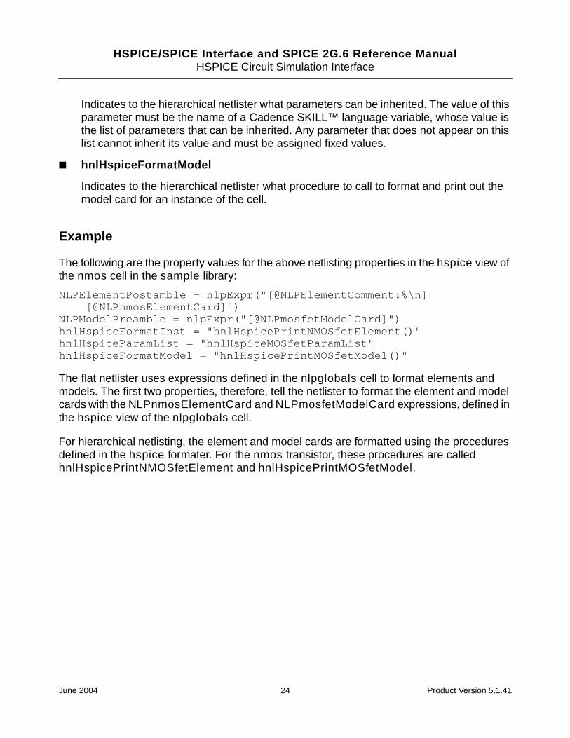
HSPICE/SPICE Interface and SPICE 2G.6 Reference ManualHSPICE Circuit Simulation Interface
Indicates to the hierarchical netlister what parameters can be inherited. The value of thisparameter must be the name of a Cadence SKILL™ language variable, whose value isthe list of parameters that can be inherited. Any parameter that does not appear on thislist cannot inherit its value and must be assigned fixed values.
■ hnlHspiceFormatModel
Indicates to the hierarchical netlister what procedure to call to format and print out themodel card for an instance of the cell.
Example
The following are the property values for the above netlisting properties in the hspice view ofthe nmos cell in the sample library:
NLPElementPostamble = nlpExpr("[@NLPElementComment:%\n][@NLPnmosElementCard]")
NLPModelPreamble = nlpExpr("[@NLPmosfetModelCard]")hnlHspiceFormatInst = "hnlHspicePrintNMOSfetElement()"hnlHspiceParamList = "hnlHspiceMOSfetParamList"hnlHspiceFormatModel = "hnlHspicePrintMOSfetModel()"
The flat netlister uses expressions defined in the nlpglobals cell to format elements andmodels. The first two properties, therefore, tell the netlister to format the element and modelcards with the NLPnmosElementCard and NLPmosfetModelCard expressions, defined inthe hspice view of the nlpglobals cell.
For hierarchical netlisting, the element and model cards are formatted using the proceduresdefined in the hspice formater. For the nmos transistor, these procedures are calledhnlHspicePrintNMOSfetElement and hnlHspicePrintMOSfetModel.
June 2004 24 Product Version 5.1.41

HSPICE/SPICE Interface and SPICE 2G.6 Reference Manual
4HSPICE/SPICE Elements
This chapter contains the following topics:
■ Overview
■ HSPICE/SPICE Elements and Corresponding Library Cells
■ HSPICE/SPICE Model and Element Parameters
■ Formatting Functions
Overview
This chapter is divided into three sections.
The first section lists the HSPICE/SPICE elements and the corresponding cells in the samplelibrary.
The second section has information about the library cells, terminal names, element andmodel parameters, for each HSPICE/SPICE element.
The third section has information about the formatting functions for each HSPICE/SPICEelement.
June 2004 25 Product Version 5.1.41

HSPICE/SPICE Interface and SPICE 2G.6 Reference ManualHSPICE/SPICE Elements
HSPICE/SPICE Elements and Corresponding LibraryCellsHSPICE/SPICE Element(Model Type) Library Cell
R res
R resistor
C cap
C capacitor
C pcapacitor
L inductor
T tline
G soi.vc
G vcisrc
E sov.vc
E vcvsrc
F soi.ic
H sov.ic
V sov
V vsrc
I soi
I isrc
D diode
D pdiode
Q(npn) npn
Q(npn) npns
Q(pnp) pnp
Q(pnp) pnps
J(njf) njfet
J(pjf) pjfet
June 2004 26 Product Version 5.1.41

HSPICE/SPICE Interface and SPICE 2G.6 Reference ManualHSPICE/SPICE Elements
HSPICE/SPICE Model and Element Parameters
Resistor
HSPICE/SPICE Element: ResistorElement Name: RUsed by Library Cells: res, resistor
M(nmos) ndepl
M(nmos) nfet
M(nmos) nmos
M(nmos) nmosd
M(nmos) nmose
M(nmos) nsftn
M(nmos) nxfr
M(pmos) pdepl
M(pmos) pfet
M(pmos) pmos
M(pmos) pmosd
M(pmos) pmose
M(pmos) psftn
M(pmos) pxfr
Terminal Name Level ofSimulation Direction
A Circuit inputOutput
Y Circuit inputOutput
HSPICE/SPICE Element(Model Type) Library Cell
June 2004 27 Product Version 5.1.41

HSPICE/SPICE Interface and SPICE 2G.6 Reference ManualHSPICE/SPICE Elements
Capacitor
HSPICE/SPICE Element: CapacitorElement Named: CUsed by Library Cells: cap, capacitor, pcapacitor
Inductor
HSPICE/SPICE Element: InductorElement Name: LUsed by Library Cell: inductor
ElementParameter Data Type Units
r float ohms
tc string --
Terminal Name Level of Simulation Direction
Y Circuit inputOutput
gnd! Circuit inputOutput
Element Parameter DataType Units
c float farads
ic string --
Terminal Name Level ofSimulation Direction
PLUS Circuit inputOutput
MINUS Circuit inputOutput
ElementParameter Data Type Units
l float henrys
June 2004 28 Product Version 5.1.41

HSPICE/SPICE Interface and SPICE 2G.6 Reference ManualHSPICE/SPICE Elements
Transmission Line
HSPICE/SPICE Element: Transmission LineElement Name: TUsed by Library Cell: tline
ic string --
Terminal Name Level ofSimulation Direction
N1 Circuit inputOutput
N2 Circuit inputOutput
N3 Circuit inputOutput
N4 Circuit inputOutput
ElementParameter Data Type Units
z0 float ohms
td float seconds
f float hertz
nl float unitless
ic string --
ElementParameter Data Type Units
June 2004 29 Product Version 5.1.41

HSPICE/SPICE Interface and SPICE 2G.6 Reference ManualHSPICE/SPICE Elements
Diode
HSPICE/SPICE Element: DiodeElement Name: DModel Type: DUsed by Library Cell: diode
Terminal Name Level ofSimulation Direction
PLUS Circuit inputOutput
MINUS Circuit inputOutput
Element Parameter Data Type Units
area float unitless
off string “off”
ic string --
Model Parameter Data Type Units
is float amperes
rs float ohms
n float unitless
tt float seconds
cjo float farads
vj float volts
m float unitless
eg float electronvolts
xti float unitless
kf float unitless
af float unitless
fc float unitless
ibv float amperes
June 2004 30 Product Version 5.1.41

HSPICE/SPICE Interface and SPICE 2G.6 Reference ManualHSPICE/SPICE Elements
BJT
HSPICE/SPICE Element: BJTElement Name: QModel Type: NPN, PNPUsed by Library Cells: npn, npns, pnp, pnps
bv float volts
Terminal Name Level of Simulation Direction
C Circuit inputOutput
B Circuit inputOutput
E Circuit inputOutput
SUB Circuit inputOutput
Element Parameter Data Type Units
area float unitless
off string “off”
ic string --
Model Parameter Data Type Units
is float amperes
bf float unitless
nf float unitless
ise float amperes
ne float unitless
br float unitless
nr float unitless
isc float amperes
Model Parameter Data Type Units
June 2004 31 Product Version 5.1.41

HSPICE/SPICE Interface and SPICE 2G.6 Reference ManualHSPICE/SPICE Elements
nc float unitless
rb float ohms
rbm float ohms
re float ohms
rc float ohms
cje float farads
vje float volts
mje float unitless
tf float seconds
xtf float unitless
itf float amperes
ptf float degrees
cjc float farads
vjc float volts
mjc float unitless
xcjc float unitless
tr float seconds
cjs float farads
vjs float volts
mjs float unitless
xtb float unitless
eg float electronvolts
xti float unitless
kf float unitless
af float unitless
fc float unitless
vtf float volts
Model Parameter Data Type Units
June 2004 32 Product Version 5.1.41

HSPICE/SPICE Interface and SPICE 2G.6 Reference ManualHSPICE/SPICE Elements
JFET
HSPICE/SPICE Element: JFETElement Name: JModel Type: NJF, PJFUsed by Libary Cells: njfet, pjfet
irb float amperes
ikr float amperes
var float volts
vaf float volts
ikf float amperes
Terminal Name Level of Simulation Direction
D Circuit inputOutput
G Circuit inputOutput
S Circuit inputOutput
ElementParameter Data Type Units
area float unitless
off string “off”
ic string --
Model Parameter Data Type Units
vto float volts
beta float amperes/square volts
lambda float 1/volts
rd float ohms
rs float ohms
Model Parameter Data Type Units
June 2004 33 Product Version 5.1.41

HSPICE/SPICE Interface and SPICE 2G.6 Reference ManualHSPICE/SPICE Elements
MOSFET
HSPICE/SPICE Element: MOSFETElement Name: MModel Type: NMOS, PMOSUsed by Library Cells: ndepl, nfet, nmos, mosd, nmose, nsftn, nxfr, pdepl, pfet, pmos, pmos, pmose, psftn, pxfr
cgs float farads
cgd float farads
pb float volts
is float amperes
kf float unitless
af float unitless
fc float unitless
Terminal Name Level of Simulation Direction
D Circuit inputOutput
G Circuit inputOutput
S Circuit inputOutput
B Circuit inputOutput
ElementParameter Data Type Units
l float meters
w float meters
ad float square meters
as float square meters
pd float meters
ps float meters
Model Parameter Data Type Units
June 2004 34 Product Version 5.1.41

HSPICE/SPICE Interface and SPICE 2G.6 Reference ManualHSPICE/SPICE Elements
nrd float unitless
nrs float unitless
off string “off”
ic string --
ModelParameter Data Type Units
level integer unitless
vto float volts
kp float amperes/volts squared
gamma float volts**0.5
phi float volts
lambda float 1/volts
rd float ohms
rs float ohms
cbd float farads
cbs float farads
is float amperes
pb float volts
cgso float farads/meter
cgdo float farads/meter
cgbo float farads/meter
rsh float ohms/square
cj float farads/square meter
mj float unitless
cjsw float farads/meter
mjsw float unitless
ElementParameter Data Type Units
June 2004 35 Product Version 5.1.41

HSPICE/SPICE Interface and SPICE 2G.6 Reference ManualHSPICE/SPICE Elements
Formatting Functions
This section describes the formatting functions included with the HSPICE/SPICE interface.The cells in the sample library that use these formatting functions are also listed. The syntax
js float amperes/square meter
tox float meters
nsub float 1/cubic centimeters
nss float 1/square centimeters
nfs float 1/square centimeters
tpg integer unitless
xj float meters
ld float meters
uo float square centimeters/voltseconds
ucrit float volts/centimeter
uexp float unitless
utra float unitless
vmax float meters/second
neff float unitless
xqc float unitless
kf float unitless
af float unitless
fc float unitless
delta float unitless
theta float 1/volts
eta float unitless
kappa float unitless
ModelParameter Data Type Units
June 2004 36 Product Version 5.1.41

HSPICE/SPICE Interface and SPICE 2G.6 Reference ManualHSPICE/SPICE Elements
for these formatting functions is that of the nlpglobal functions, but the same parameters arealso defined in the hspice formatter for hierarchical netlisting.
This section uses the following notations:
<...> name in the brackets is an identifier
{...} item(s) in braces can be repeated as many times as necessary
[...] item(s) in brackets are optional
@name value of property name is substituted
Element Formats
Below is the list of HSPICE/SPICE elements and their formats:
res
r<name> <A> <Y> @r @ns @tc1 @tc2 @scale @rsh ac=@ac m=@m
The res cell in the sample library uses this format.
resistor
r<name> <PLUS> <MINUS> @r @ns @tc1 @tc2 @scale @rsh ac=@ac m=@m
The resistor cell in the sample library uses this format.
cap
c<name> <Y> gnd! @c @ns @tc1 @tc2 @scale @cj ic=@ic m=@m
The cap cell in the sample library uses this format.
capacitor
c<name> <PLUS> <MINUS> @c @ns @tc1 @tc2 @scale @cj ic=@ic m=@m
The capacitor and pcapacitor cells in the sample library use this format.
June 2004 37 Product Version 5.1.41

HSPICE/SPICE Interface and SPICE 2G.6 Reference ManualHSPICE/SPICE Elements
inductor
l<name> <PLUS> <MINUS> @l @tc1 @tc2 @nt ic=@ic
The inductor cell in the sample library uses this format.
transmission line
t<name> <N1> <N2> <N3> <N4> z0=@z0 td=@td f=@f nl=@nl ic=@ic
The tline cell in the sample library uses this format.
diode
d<name> <PLUS> <MINUS> <cellName> w=@w l=@l area=@area pj=@pj wp=@wplp=@lp wm=@wm lm=@lm @off ic=@ic m=@m
The diode and pdiode cells in the sample library use this format.
BJT
q<name> <C> <B> <E> <SUB> <cellName> area=@area @off ic=@ic m=@m
The npns and pnps cells in the sample library use this format.
JFET
j<name> <D> <G> <S> <cellName> area=@area w=@w l=@l @off ic=@ic m=@m
The njfet and pjfet cells in the sample library use this format.
MOSfet
m<name> <D> <G> <S> <B> <cellName> w=@w l=@l ad=@ad as=@as pd=@pdps=@ps nrd=@nrd nrs=@nrs off" off ic=@ic m=@m
The ndepl, nfet, nsftn, pdepl, pfet, and psftn cells in the sample library use this format.
NMOSfet
m<name> <D> <G> <S> gnd! <cellName> w=@w l=@l ad=@ad as=@as pd=@pd ps=@ps nrd=@nrdnrs=@nrs off" off ic=@ic m=@m
June 2004 38 Product Version 5.1.41

HSPICE/SPICE Interface and SPICE 2G.6 Reference ManualHSPICE/SPICE Elements
The nxfr, nmos, nmosd, and nmose cells in the sample library use this format.
NPN
q<name> <C> <B> <E> vee! <cellName> area=@area off" off ic=@ic m=@m
The npn cell in the sample library uses this format.
PMOSfet
"m<name> <D> <G> <S> vdd! <cellName> w=@w l=@l ad=@ad as=@as pd=@pd ps=@ps nrd=@nrdnrs=@nrs off" off ic=@ic m=@m
The pxfr, pmos, pmosd, and pmose cells in the sample library use this format.
PNP
"q<name> <C> <B> <E> vcc! <cellName> @area off" off ic=@ic m=@m
The pnp cell in the sample library uses this format.
Model Format
Below is the list of HSPICE/SPICE models and their model card format.
Diode
.model <cellName> d level=@level area=@area eg=@eg is=@is jsw=@jsw n=@n pj=@pjtlev=@tlev xti=@xti ibv=@ibv tcv=@tcv vb=@vb af=@af kf=@kf rs=@rs trs=@trscjo=@cjo cjp=@cjp cta=@cta ctp=@ctp fc=@fc fcs=@fcs m=@m mjsw=@mjsw pb=@pbphp=@php tt=@tt ef=@ef er=@er jf=@jf jr=@jr w=@w l=@l tox=@tox wm=@wm lm=@lmwp=@wp lp=@lp xm=@xm xp=@xp xoi=@xoi xom=@xom
The diode and pdiode cells in the sample library use this format.
BJT
.model <cellName> @modelType bf=@bf br=@br bulk=@bulk eg=@eg is=@is iss=@iss nf=@nfnr=@nr subs=@subs isc=@isc ise=@ise nc=@nc ne=@ne vaf=@vaf var=@var ikf=@ikfikr=@ikr irb=@irb rb=@rb rbm=@rbm re=@re rc=@rc cjc=@cjc cje=@cje cjs=@cjsfc=@fc mjc=@mjc mje=@mje mjs=@mjs vjc=@vjc vje=@vje vjs=@vjs xcjc=@xcjc
June 2004 39 Product Version 5.1.41

HSPICE/SPICE Interface and SPICE 2G.6 Reference ManualHSPICE/SPICE Elements
itf=@itf ptf=@ptf tf=@tf tr=@tr vtf=@vtf xtf=@xtf tlev=@tlev tre1=@tre1tre2=@tre2 trb1=@trb1 trb2=@trb2 trc1=@trc1 trc2=@trc2 trm1=@trm1 trm2=@trm2xtb=@xtb xti=@xti af=@af kf=@kf
The npn, npns, pnp, and pnps cells in the sample library use this format.
JFET
.model <cellName> @modelType level=%s" level a=@a alpha=@alpha beta=@beta d=@dgamds=@gamds lambda=@lambda w=@w l=@l wdel=@wdel ldel=@ldel tcv=@tcv vto=@vtoeg=@eg gap1=@gap1 gap2=@gap2 is=@is n=@n ni=@ni xti=@xti af=@af kf=@kf rd=@rdrg=@rg rs=@rs trd=@trd trg=@trg trs=@trs cgd=@cgd cgs=@cgs fc=@fc m=@m pb=@pbcapop=@capop ctd=@ctd cts=@cts tt=@tt bex=@bex lam1=@lam1 nchan=@nchansat=@sat ucrit=@ucrit vbi=@vbi vgexp=@vgexp vp=@vp tlev=@tlev tlevc=@tlevctpb=@tpb
The njfet and pjfet cells in the sample library use this format.
MOSfet
.model<cellName> @modelType level=@level vto=@vto nss=@nss tpg=@tpg phi=@phigamma=@gamma nsub=@nsub bulk=@bulk bex=@bex kp=@kp lambda=@lambdaecrit=@ecrit neff=@neff nfs=@nfs ucrit=@ucrit uexp=@uexp uo=@uo utra=@utravmax=@vmax xj=@xj ld=@ld theta=@theta clm=@clm dns=@dns fds=@fds mbl=@mblmob=@mob nu=@nu nwe=@nwe nwm=@nwm scm=@scm tcv=@tcv ufds=@ufds vbo=@vbovfds=@vfds vsh=@vsh wic=@wic f1=@f1 mob=@mob af=@af kf=@kf cgbo=@cgbocgdo=@cgdo cgso=@cgso cox=@cox meto=@meto tox=@tox wd=@wd capop=@capopcf1=@cf1 cf2=@cf2 cf3=@cf3 cf4=@cf4 cf5=@cf5 cf6=@cf6 alpha=@alpha is=@isjs=@js jsw=@jsw vcr=@vcr cbd=@cbd cbs=@cbs cj=@cj cjsw=@cjsw mj=@mjmjsw=@mjsw pb=@pb php=@php ldif=@ldif rd=@rd rs=@rs rsh=@rsh trd=@trdtrs=@trs delta=@delta kappa=@kappa eta=@eta
The ndepl, nfet, nmos, nmosd, nmose, nsftn, nxfr, pdepl, pfet, pmos, pmosd, pmose,psftn, and pxfr cells in the sample library use this format.
June 2004 40 Product Version 5.1.41
HSPICE/SPICE Interface and SPICE 2G.6 Reference Manual
5Using SPICE
This chapter contains the following topics:
■ Introduction
■ Types of Analysis
■ Convergence
■ Input Format
■ Circuit Description
■ Title Card, Comment Cards, and .END Card
■ Element Cards for Passive Circuit Elements and Sources
■ Semiconductor Devices
■ Element Cards for Semiconductor Devices
■ MODEL Cards for Semiconductor Devices
■ Subcircuits
■ Control Cards
■ Example of Data Decks
■ Nonlinear Dependent Sources
■ Bipolar Model Equations (Gmin terms omitted)
■ Alter Statement and the Source-Stepping Method
■ References
June 2004 41 Product Version 5.1.41
HSPICE/SPICE Interface and SPICE 2G.6 Reference ManualUsing SPICE
Introduction
SPICE is a general-purpose circuit simulation program for nonlinear DC, nonlinear transient,and linear AC analyses. Circuits may contain resistors, capacitors, inductors, mutualinductors, independent voltage and current sources, four types of dependent sources,transmission lines, and the four most common semiconductor devices: diodes, BJTs, JFETs,and MOSFETs.
SPICE has built-in models for the semiconductor devices, and the user need specify only thepertinent model parameter values. The model for the BJT is based on the integral chargemodel of Gummel and Poon; however, if the Gummel-Poon parameters are not specified, themodel reduces to the simpler Ebers-Moll model. In either case, charge storage effects, ohmicresistances, and a current-dependent output conductance may be included.
The diode model can be used for either junction diodes or Schottky barrier diodes. The JFETmodel is based on the FET model of Shichman and Hodges. Three MOSFET models areimplemented: MOS1 is described by a square-law I-V characteristic, MOS2 is an analyticalmodel, while MOS3 is a semi-empirical model. Both MOS2 and MOS3 include second-ordereffects such as channel length modulation, subthreshold conduction, scattering limitedvelocity saturation, small-size effects and charge-controlled capacitances.
Types of Analysis
DC Analysis
The DC analysis portion of SPICE determines the dc operating point of the circuit withinductors shorted and capacitors opened. A DC analysis is automatically performed prior toa transient analysis to determine the transient initial conditions and prior to an AC small-signalanalysis to determine the linearized, small-signal models for nonlinear devices. If requested,the DC small-signal value of a transfer function (ratio of output variable to input source), inputresistance, and output resistance will also be computed as a part of the DC solution. The DCanalysis can also be used to generate DC transfer curves: a specifie DC output variables arestored for each sequential source value. If requested, SPICE also will determine the DCsmall-signal sensitivities of specified output variables with respect to circuit parameters. TheDC analysis options are specified on the .DC, .TF, .OP, and .SENS control cards.
To see the small-signal models for nonlinear devices in conjunction with a transient analysisoperating point, the .OP card must be provided. The DC bias conditions will be identical foreach case, but the more comprehensive operating point information is not available to beprinted when transient initial conditions are computed.
June 2004 42 Product Version 5.1.41

HSPICE/SPICE Interface and SPICE 2G.6 Reference ManualUsing SPICE
AC Small-Signal Analysis
The AC small-signal portion of SPICE computes the AC output variables as a function offrequency. The program first computes the DC operating point of the circuit and determineslinearized, small-signal models for all of the nonlinear devices in the circuit. The resultantlinear circuit is then analyzed over a user-specified range of frequencies. The desired outputof an AC small-signal analysis is usually a transfer function (voltage gain, transimpedance,etc.). If the circuit has only one AC input, it is convenient to set that input to unity and zerophase so that output variables have the same value as the transfer function of the outputvariable with respect to the input.
The generation of white noise by resistors and semiconductor devices can also be simulatedwith the AC small-signal portion of SPICE. Equivalent noise source values are determinedautomatically from the small-signal operating point of the circuit, and the contribution of eachnoise source is added at a given summing point. The total output noise level and theequivalent input noise level are determined at each frequency point. The output and inputnoise levels are normalized with respect to the square root of the noise bandwidth and havethe units Volts/rt Hz or Amps/rt Hz. The output noise and equivalent input noise can be printedor plotted in the same fashion as other output variables. No additional input data is necessaryfor this analysis.
Flicker noise sources can be simulated in the noise analysis by including values for theparameters KF and AF on the appropriate device model cards.
The distortion characteristics of a circuit in the small-signal mode can be simulated as a partof the AC small-signal analysis. The analysis is performed assuming that one or two signalfrequencies are imposed at the input.
The frequency range and the noise and distortion analysis parameters are specified on the.AC, .NOISE, and .DISTO control lines.
Transient Analysis
The transient analysis portion of SPICE computes the transient output variables as a functionof time over a user-specified time interval. The initial conditions are automatically determinedby a dc analysis. All sources that are not time dependent (for example, power supplies) areset to their DC value. For large-signal sinusoidal simulations, a Fourier analysis of the outputwaveform can be specified to obtain the frequency domain Fourier coefficients. The transienttime interval and the Fourier analysis options are specified on the .TRAN and .FOURIERcontrol lines.
June 2004 43 Product Version 5.1.41
HSPICE/SPICE Interface and SPICE 2G.6 Reference ManualUsing SPICE
Analysis at Different Temperatures
All input data for SPICE is assumed to have been measured at 27 (300 K). Thesimulation also assumes a nominal temperature of 27 . The circuit can be simulated atother temperatures by using a .TEMP control line.
Temperature appears explicitly in the exponential terms of the BJT and diode modelequations. In addition, saturation currents have a built-in temperature dependence. Thetemperature dependence of the saturation current in the BJT models is determined by
IS(T1) = IS(T0)*((T1/T0**XTI)*exp(q*EG*(T1-T0)/(k*T1*T0))
where k is Boltzmann’s constant; q is the electronic charge;EG is the energy gap, which is amodel parameter; and XTI is the saturation current temperature exponent (also a modelparameter, and usually equal to 3). The temperature dependence of forward and reverse betais according to the formula
beta(T1)=beta(T0)*(T1/T0)**XTB
where T1 and T0 are in degrees Kelvin and XTB is a user-supplied model parameter.Temperature effects on beta are carried out by appropriate adjustment to the values of BF,ISE, BR, and ISC. Temperature dependence of the saturation current in the junction diodemodel is determined by
IS(T1) = IS(T0)*((T1/T0)**(XTI/N))*exp(q*EG*(T1-T0)/(k*N*T1*T0))
where N is the emission coefficient, which is a model parameter, and the other symbols havethe same meaning as above.
Note: For Schottky barrier diodes, the value of the saturation current temperature exponent,XTI, is usually 2.
Temperature appears explicitly in the value of junction potential, PHI, for all the devicemodels. The temperature dependence is determined by
PHI(TEMP) = k*TEMP/q*log(Na*Nd/Ni(TEMP)**2)
where k is Boltzmann’s constant, q is the electronic charge, Na is the acceptor impuritydensity, Nd is the donor impurity density, Ni is the intrinsic concentration, and EG is theenergy gap.
Temperature appears explicitly in the value of surface mobility, UO, for the MOSFET model.The temperature dependence is determined by
°C
°C
June 2004 44 Product Version 5.1.41

HSPICE/SPICE Interface and SPICE 2G.6 Reference ManualUsing SPICE
UO(TEMP) = UO(TNOM)/(TEMP/TNOM)**(1.5)
The effects of temperature on resistors is modeled by the formula
value(TEMP) = value(TNOM)*(1+TC1*(TEMP-TNOM)+TC2*(TEMP-TNOM) **2))
where TEMP is the circuit temperature, TNOM is the nominal temperature, and TC1 and TC2are the first- and second-order temperature coefficients.
Convergence
Both DC and transient solutions are obtained by an iterative process, which is terminatedwhen both of the following conditions hold:
1. The non linear branch currents converge to within a tolerance of 0.1 percent or 1picoamp (1.0E-12 Amp), whichever is larger.
2. The node voltages converge to within a tolerance of 0.1 percent or 1 microvolt (1.0E-6Volt), whichever is larger.
Although the algorithm used in SPICE has been found to be very reliable, in some cases itwill fail to converge to a solution. When this failure occurs, the program will print the nodevoltages at the last iteration and terminate the job. In such cases, the node voltages that areprinted are not necessarily correct or even close to the correct solution.
Failure to converge in the DC analysis is usually due to an error in specifying circuitconnections, element values, or model parameter values. Regenerative switching circuits orcircuits with positive feedback probably will not converge in the DC analysis unless the OFFoption is used for some of the devices in the feedback path, or the .NODESET card is usedto force the circuit to converge to the desired state.
Input Format
The input format for SPICE is of the free format type. Fields on a card are separated by oneor more blanks, a comma, an equal (=) sign, or a left or right parenthesis; extra spaces areignored. A card may be continued by entering a + (plus) in column 1 of the following card;SPICE continues reading beginning with column 2.
A name field must begin with a letter (A through Z) and cannot contain any delimiters. Onlythe first eight characters of the name are used.
June 2004 45 Product Version 5.1.41

HSPICE/SPICE Interface and SPICE 2G.6 Reference ManualUsing SPICE
A number field may be an integer field (12, -44), a floating point field (3.14159), either aninteger or floating point number followed by an integer exponent (1E-14, 2.65E3), or either aninteger or a floating point number followed by one of the following scale factors:
T=1E12
G=1E9
MEG=1E6
K=1E3
MIL=25.4E-6
M=1E-3
U=1E-6
N=1E-9
P=1E-12
F=1E-15
Letters immediately following a number that are not scale factors are ignored, and lettersimmediately following a scale factor are ignored. Hence, 10, 10V, 10VOLTS, and 10HZ allrepresent the same number, and M, MA, MSEC, and MMHOS all represent the same scalefactor. (Note that 1000, 1000.0, 1000HZ, 1E3, 1.0E3, 1KHZ, and 1K all represent the samenumber.)
Circuit Description
The circuit to be analyzed is described to SPICE by a set of element cards, which define thecircuit topology and element values, and a set of control cards, which define the modelparameters and the run controls. The first card in the input deck must be a title card, and thelast card must be an .END card. The order of the remaining cards is arbitrary (except, ofcourse, that continuation cards must immediately follow the card being continued).
Each element in the circuit is specified by an element card that contains the element name,the circuit nodes to which the element is connected, and the values of the parameters thatdetermine the electrical characteristics of the element. The first letter of the element namespecifies the element type. The format for the SPICE element types is given in what follows.The strings XXXXXXX, YYYYYYY, and ZZZZZZZ denote arbitrary alphanumeric strings. Forexample, a resistor name must begin with the letter R and can contain from one to eightcharacters. Hence, R, R1, RSE, ROUT, and R3AC2ZY are valid resistor names.
June 2004 46 Product Version 5.1.41

HSPICE/SPICE Interface and SPICE 2G.6 Reference ManualUsing SPICE
Data fields that are enclosed in < > are optional. All indicated punctuation (parentheses,equal signs, etc.) are required. With respect to branch voltages and currents, SPICEuniformly uses the associated reference convention (current flows in the direction of voltagedrop).
Nodes must be nonnegative integers but need not be numbered sequentially. The datum(ground) node must be numbered 0. The circuit cannot contain a loop of voltage sources and/or inductors and cannot contain a cutset of current sources and/or capacitors. Each node inthe circuit must have a DC path to ground. Every node must have at least two connectionsexcept for transmission line nodes (to permit unterminated transmission lines) and MOSFETsubstrate nodes (which have two internal connections anyway).
Title Card, Comment Cards, and .END Card
Title Card
Examples:
POWER AMPLIFIER CIRCUITTEST OF CAM CELL
This card must be the first card in the input deck. Its contents are printed verbatim as theheading for each section of output.
.END Card
Examples:
.END
This card must always be the last card in the input deck. Note that the period is an integralpart of the name.
Comment Card
General Form:
* <any comment>
Examples:
* RF=1K GAIN SHOULD BE 100
June 2004 47 Product Version 5.1.41

HSPICE/SPICE Interface and SPICE 2G.6 Reference ManualUsing SPICE
* MAY THE FORCE BE WITH MY CIRCUIT
The asterisk in the first column indicates that this card is a comment card. Comment cardsmay be placed anywhere in the circuit description.
Element Cards for Passive Circuit Elements and Sources
Resistors
General form:
RXXXXXXX N1 N2 VALUE <TC=TC1,<TC2>>
Examples:
R1 1 2 100RC1 12 17 1K TC=0.001,0.015
N1 and N2 are the two element nodes. VALUE is the resistance (in ohms) and may be positiveor negative but not zero. TC1 and TC2 are the (optional) temperature coefficients; if notspecified, zero is assumed for both. The value of the resistor as a function of temperature isgiven by:
value(TEMP)=value(TNOM)*(1+TC1*(TEMP-TNOM)+TC2*(TEMP-TNOM)**2))
Capacitors and Inductors
General form:
CXXXXXXX N+ N- VALUE <IC=INCOND>LYYYYYYY N+ N- VALUE <IC=INCOND>
Examples:
CBYP 13 0 1UFCOSC 17 23 10U IC=3VLLINK 42 69 1UHLSHUNT 23 51 10U IC=15.7MA
N+ and N- are the positive and negative element nodes, respectively. VALUE is thecapacitance in Farads or the inductance in Henries.
June 2004 48 Product Version 5.1.41

HSPICE/SPICE Interface and SPICE 2G.6 Reference ManualUsing SPICE
For the capacitor, the (optional) initial condition is the initial (time-zero) value of capacitorvoltage (in Volts). For the inductor, the (optional) initial condition is the initial (time-zero) valueof inductor current (in Amps) that flows from N+, through the inductor, to N-.
Note: The initial conditions (if any) apply only if the UIC option is specified on the .TRAN card.
Nonlinear capacitors and inductors can be described.
General form:
CXXXXXXX N+ N- POLY C0 C1 C2 . . . <IC=INCOND>LYYYYYYY N+ N- POLY L0 L1 L2 . . . <IC=INCOND>
C0 C1 C2 . . . (and L0 L1 L2 . . .) are the coefficients of a polynomial describing the elementvalue. The capacitance is expressed as a function of the voltage across the element while theinductance is a function of the current through the inductor. The value is computed as
value=C0+C1*V+C2*V**2+. . .value=L0+L1*I+L2*I**2+. . .
where V is the voltage across the capacitor and I the current flowing in the inductor.
Coupled (Mutual) Inductors
General form:
KXXXXXXX LYYYYYYY LZZZZZZZ VALUE
Examples:
K43 LAA LBB 0.999KXFRMR L1 L2 0.87
LYYYYYYY and LZZZZZZZ are the names of the two coupled inductors, and VALUE is thecoefficient of coupling, K, which must be greater than 0 and less than or equal to 1. Using the‘dot’ convention, place a ‘dot’ on the first node of each inductor.
Transmission Lines (Lossless)
General form:
TXXXXXXX N1 N2 N3 N4 Z0=VALUE <TD=VALUE> <F=FREQ +<NL=NRMLEN>><IC=V1,I1,V2,I2>
Examples:
June 2004 49 Product Version 5.1.41

HSPICE/SPICE Interface and SPICE 2G.6 Reference ManualUsing SPICE
T1 1 0 2 0 Z0=50 TD=10NS
N1 and N2 are the nodes at port 1; N3 and N4 are the nodes at port 2. Z0 is the characteristicimpedance. The length of the line may be expressed in either of two forms. The transmissiondelay, TD, may be specified directly (as TD=10ns, for example). Alternatively, a frequency Fmay be given, together with NL, the normalized electrical length of the transmission line withrespect to the wavelength in the line at the frequency F. If a frequency is specified but NL isomitted, 0.25 is the assumed (that is, the frequency assumed to be the quarter-wavefrequency).
Note: Although both forms for expressing the line length are indicated as optional, one of thetwo must be specified.
Note: This element models only one propagating mode. If all four nodes are distinct in theactual circuit, two modes may be excited. To simulate such a situation, two transmission-lineelements are required. See Example of Data Decks for further clarification.
The (optional) initial condition specification consists of the voltage and current at each of thetransmission line ports.
Note: The initial conditions (if any) apply only if the UIC option is specified on the .TRAN card.
One should be aware that SPICE will use a transient time-step that does not exceed 1/2 theminimum transmission line delay. Therefore, very short transmission lines (compared with theanalysis time frame) will cause long run times.
Linear Dependent Sources
SPICE allows circuits to contain linear dependent sources characterized by any of the fourequations
i=g*v v=e*v i=f*i v=h*i
where g, e, f, and h are constants representing transconductance, voltage gain, current gain,and transresistance, respectively. See Nonlinear Dependent Sources for a more completedescription of dependent sources as implemented in SPICE.
Linear Voltage-Controlled Current Sources
General form:
GXXXXXXX N+ N- NC+ NC- VALUE
Examples:
June 2004 50 Product Version 5.1.41

HSPICE/SPICE Interface and SPICE 2G.6 Reference ManualUsing SPICE
G1 2 0 5 0 0.1MMHO
N+ and N- are the positive and negative nodes, respectively. Current flow is from the positivenode, through the source, to the negative node. NC+ and NC- are the positive and negativecontrolling nodes, respectively. VALUE is the transconductance (in ohms).
Linear Voltage-Controlled Voltage Sources
General form:
EXXXXXXX N+ N- NC+ NC- VALUE
Examples:
E1 2 3 14 1 2.0
N+ is the positive node and N- is the negative node. NC+ and NC- are the positive andnegative controlling nodes, respectively. VALUE is the voltage gain.
Note: If the "value" property is not defined, then the value of "gain" is printed. The "value"property is printed, in case it is defined instead of "gain".
Linear Current-Controlled Current Sources
General form:
FXXXXXXX N+ N- VNAM VALUE
Examples:
F1 13 5 VSENS 5
N+ and N- are the positive and negative nodes, respectively. Current flow is from the positivenode, through the source, to the negative node. VNAM is the name of a voltage sourcethrough which the controlling current flows. The direction of positive controlling current flowis from the positive node, through the source, to the negative node of VNAM. VALUE is thecurrent gain.
Linear Current-Controlled Voltage Sources
General form:
HXXXXXXX N+ N- VNAM VALUE
Examples:
HX 5 17 VZ 0.5K
June 2004 51 Product Version 5.1.41

HSPICE/SPICE Interface and SPICE 2G.6 Reference ManualUsing SPICE
N+ and N- are the positive and negative nodes, respectively. VNAM is the name of the voltagesource through which the controlling current flows. The direction of positive controlling currentflow is from the positive node, through the source, to the negative node of VNAM. VALUE isthe transresistance (in ohms).
Independent Sources
General form:
VXXXXXXX N+ N- <<DC>DC/TRAN VALUE> <AC <ACMAG <ACPHASE>>>IYYYYYYY N+ N- <<DC>DC/TRAN VALUE> <AC <ACMAG <ACPHASE>>>
Examples:
VCC 10 0 DC 6VIN 13 2 0.001 AC 1 SIN(0 1 1MEG)ISRC 23 21 AC 0.333 45.0 SFFM(0 1 10K 5 1K)VMEAS 12 9
N+ and N- are the positive and negative nodes, respectively.
Note: Voltage sources need not be grounded. Positive current is assumed to flow from thepositive node, through the source, to the negative node. A current source of positive value willforce current to flow out of the N+ node, through the source, and into the N- node. Voltagesources, in addition to being used for circuit excitation, are the ammeters for SPICE; that is,zero-valued voltage sources may be inserted into the circuit for the purpose of measuringcurrent. They will, of course, have no effect on circuit operation since they represent short-circuits.
DC/TRAN is the DC and transient analysis value of the source. If the source value is zero bothfor DCand transient analyses, this value may be omitted. If the source value is time-invariant(for example, a power supply), then the value may optionally be preceded by the letters DC.
ACMAG is the AC magnitude and ACPHASE is the AC phase. The source is set to this valuein the AC analysis. If ACMAG is omitted following the keyword AC, a value of unity isassumed. If ACPHASE is omitted, a value of zero is assumed. If the source is not an ACsmall-signal input, the keyword AC and the AC values are omitted.
Any independent source can be assigned a time-dependent value for transient analysis. If asource is assigned a time-dependent value, the time-zero value is used for DC analysis.There are five independent source functions: pulse, exponential, sinusoidal, piece-wiselinear, and single-frequency FM. If parameters other than source values are omitted or set to0, the default values shown will be assumed. (TSTEP is the printing increment and TSTOP isthe final time. See the .TRAN card for explanation.)
June 2004 52 Product Version 5.1.41

HSPICE/SPICE Interface and SPICE 2G.6 Reference ManualUsing SPICE
Pulse
PULSE(V1 V2 TD TR TF PW PER)
Examples:
VIN 3 0 PULSE(-1 1 2NS 2NS 2NS 50NS 100NS)
A single pulse so specified is described by the following table:
Intermediate points are determined by linear interpolation.
Sinusoidal
SIN(VO VA FREQ TD THETA)
Examples:
Parameters Default Values Units
V1 (initial value) - Volts
V2 (pulsed value) - Volts or Amps
TD (delay time) 0.0 seconds
TR (rise time) TSTEP seconds
TF (fall time) TSTEP seconds
PW (pulse width) TSTOP seconds
PER (period) TSTOP seconds
Time Value
0 V1
TD V1
TD+TR V2
TD+TR+PW V2
TD+TR+PW+TF V1
TSTOP V1
June 2004 53 Product Version 5.1.41

HSPICE/SPICE Interface and SPICE 2G.6 Reference ManualUsing SPICE
VIN 3 0 SIN(0 1 100MEG 1NS 1E10)
The shape of the waveform is described by the following table:
Exponential
EXP(V1 V2 TD1 TAU1 TD2 TAU2)
Examples:
VIN 3 0 EXP(-4 -1 2NS 30NS 60NS 40NS)
Parameters Default Values Units
VO (offset) - Volts or Amps
VA (amplitude) - Volts or Amps
FREQ (frequency) 1/TSTOP Hz
TD (delay) 0.0 seconds
THETA (damping factor) 0.0 1/seconds
Time Value
0 to TD VO
TD to TSTOP VO + VA*exp(-(time-TD)*THETA)*sine(twopi*FREQ*(time+TD))
Parameters Default Values Units
V1 (initial value) - Volts or Amps
V2 (pulsed value) - Volts or Amps
TD1 (rise time delay) 0.0 seconds
TAU1 (rise time constant) TSTEP seconds
TD2 (fall delay time) TD1+TSTEP seconds
TAU2 (fall time constant) TSTEP seconds
June 2004 54 Product Version 5.1.41

HSPICE/SPICE Interface and SPICE 2G.6 Reference ManualUsing SPICE
The shape of the waveform is described by the following table:
Piece-Wise Linear
PWL(T1 V1 <T2 V2 T3 V3 T4 V4 . . .>)
Examples:
VCLOCK 7 5 PWL(0-7 10NS-7 11NS-3 17NS-3 18NS-7 50NS-7)
Each pair of values (Ti, Vi) specifies that the value of the source is Vi (in Volts or Amps) attime=Ti. The value of the source at intermediate values of time is determined by using linearinterpolation on the input values.
Single-Frequency FM
SFFM(VO VA FC MDI FS)
Examples:
V1 12 0 SFFM(0 1M 20K 5 1K
The shape of the waveform is described by the following equation:
value = VO + VA*sine((twopi*FC*time) + MDI*sine(twopi*FS*time))
Time Value
0 to TD1 V1
TD1 to TD2 V1+(V2-V1)*(1-exp(-(time-TD1)/TAU1))
TD2 to TSTOP V1+(V2-V1)*(1-exp(-(time-TD1)TAU1)) +(V1-V2)*(1-exp(-(time-TD2)/TAU2))
Parameters Default Values Units
VO (offset) - Volts or Amps
VA (amplitude) - Volts or Amps
FC (carrier frequency) 1/TSTOP Hz
MDI (modulation index) - -
FS (signal frequency) 1/TSTOP Hz
June 2004 55 Product Version 5.1.41

HSPICE/SPICE Interface and SPICE 2G.6 Reference ManualUsing SPICE
Semiconductor Devices
The models for the four semiconductor devices that are included in the SPICE programrequire many parameter values. Moreover, many devices in a circuit often are defined by thesame set of device model parameters. For these reasons, a set of device model parametersis defined on a separate .MODEL card and assigned a unique model name. The deviceelement cards in SPICE then reference the model name. This scheme alleviates the need tospecify all of the model parameters on each device element card.
Each device element card contains the device name, the nodes to which the device isconnected, and the device model name. In addition, other optional parameters may bespecified for each device: geometric factors and an initial condition.
The area factor used on the diode, BJT, and JFET device cards determine the number ofequivalent parallel devices of a specified model. The affected parameters are marked with anasterisk under the heading area in the model descriptions below. Several geometric factorsassociated with the channel and the drain and source diffusions can be specified on theMOSFET device card.
Two different forms of initial conditions may be specified for the devices. The first form isincluded to improve the DC convergence for circuits that contain more than one stable state.If a device is specified OFF, the DC operating point is determined with the terminal voltagesfor that device set to 0. After convergence is obtained, the program continues to iterate toobtain the exact value for the terminal voltages. If a circuit has more than one DC stable state,the OFF option can be used to force the solution to correspond to a desired state. If a deviceis specified OFF when in reality the device is conducting, the program will still obtain thecorrect solution (assuming the solutions converge) but more iterations will be requiredbecause the program must independently converge to two separate solutions. The.NODESET card serves a similar purpose as the OFF option. The .NODESET option is easierto apply and is the preferred means to aid convergence.
The second form of initial conditions are specified for use with the transient analysis. Theseare true initial conditions as opposed to the convergence aids above. (See the description ofthe .IC card and the .TRAN card for a detailed explanation of initial conditions.)
Element Cards for Semiconductor Devices
Junction Diodes
General form:
June 2004 56 Product Version 5.1.41

HSPICE/SPICE Interface and SPICE 2G.6 Reference ManualUsing SPICE
DXXXXXXX N+ N- MNAME <AREA> <OFF> <IC=VD>
Examples:
DBRIDGE 2 10 DIODE1DCLMP 3 7 DMOD 3.0 IC=0.2
N+ and N- are the positive and negative nodes, respectively. MNAME is the model name,AREA is the area factor, and OFF indicates an (optional) starting condition on the device forDC analysis. If the area factor is omitted, a value of 1.0 is assumed. The (optional) initialcondition specification using IC=VD is intended for use with the UIC option on the .TRANcard, when a transient analysis is desired starting from other than the quiescent operatingpoint.
Bipolar Junction Transistors (BJT)
General form:
QXXXXXXX NC NB NE <NS> MNAME <AREA> <OFF> <IC=VBE,VCE>
Examples:
Q23 10 24 13 QMOD IC=0.6,5.0Q50A 11 26 4 20 MOD1
NC, NB, and NE are the collector, base, and emitter nodes, respectively. NS is the (optional)substrate node. If unspecified, ground is used. MNAME is the model name, AREA is the areafactor, and OFF indicates an (optional) initial condition on the device for DC analysis. If thearea factor is omitted, a value of 1.0 is assumed. The (optional) initial condition specificationusing IC=VBE,VCE is intended for use with the UIC option on the .TRAN card, when atransient analysis is desired starting from other than the quiescent operating point. (See the.IC card description for a better way to set transient initial conditions.)
Junction Field-Effect Transistors (JFET)
General form:
JXXXXXXX ND NG NS MNAME <AREA> <OFF> <IC=VDS,VGS>
Examples:
J1 7 2 3 JM1 OFF
ND, NG, and NS are the drain, gate, and source nodes, respectively. MNAME is the modelname, AREA is the area factor, and OFF indicates an (optional) initial condition on the devicefor DC analysis. If the area factor is omitted, a value of 1.0 is assumed. The (optional) initial
June 2004 57 Product Version 5.1.41

HSPICE/SPICE Interface and SPICE 2G.6 Reference ManualUsing SPICE
condition specification, using IC=VDS,VGS is intended for use with the UIC option on the.TRAN card, when a transient analysis is desired starting from other than the quiescentoperating point. (See the .IC card for a better way to set initial conditions.)
MOSFET
General form:
MXXXXXXX ND NG NS NB MNAME <L=VAL> <W=VAL> <AD=VAL> <AS=VAL> <PD=VAL><PS=VAL> <NRD=VAL> <NRS=VAL> <OFF> + <IC=VDS,VGS,VBS>
Examples:
M1 24 2 0 20 TYPE1M31 2 17 6 10 MODM L=5U W=2UM31 2 16 6 10 MODM 5U 2UM1 2 9 3 0 MOD1 L=10U W=5U AD=100P AS=100P PD=40U PS=40UM1 2 9 3 0 MOD1 10U 5U 2P 2P
ND, NG, NS, and NB are the drain, gate, source, and bulk (substrate) nodes, respectively.MNAME is the model name. L and W are the channel length and width, in meters. AD andAS are the areas of the drain and source diffusions, in square meters. Note that the suffix Uspecifies microns (1E-6 m) and P square-microns (1E-12 sq-m). If any of L, W, AD, or AS arenot specified, default values are used. The user may specify the values to be used for thesedefault parameters on the .OPTIONS card.
The use of defaults simplifies input deck preparation, as well as the editing required if devicegeometries are to be changed. PD and PS are the perimeters of the drain and sourcejunctions, in meters. NRD and NRS designate the equivalent number of squares of the drainand source diffusions; these values multiply the sheet resistance RSH specified on the.MODEL card for an accurate representation of the parasitic series drain and sourceresistance of each transistor. PD and PS default to 0.0 ; NRD and NRS to 1.0. OFF indicatesan (optional) initial condition on the device for dc analysis.
The (optional) initial condition specification using IC=VDS,VGS,VBS is intended for use withthe UIC option on the .TRAN card, when a transient analysis is desired starting from otherthan the quiescent operating point. (See the .IC card for a better and more convenient way tospecify transient initial conditions.)
June 2004 58 Product Version 5.1.41

HSPICE/SPICE Interface and SPICE 2G.6 Reference ManualUsing SPICE
MODEL Cards for Semiconductor Devices
.MODEL Card
General form:
.MODEL MNAME TYPE(PNAME1=PVAL1 PNAME2=PVAL2 . . .)
Examples:
.MODEL MOD1 NPN BF=50 IS =1E-13 VBF=50
The .MODEL card specifies a set of model parameters that will be used by one or moredevices. MNAME is the model name, and TYPE is one of the following seven types:
Parameter values are defined by appending the parameter name, as given below for eachmodel type, followed by an equal sign and the parameter value. Model parameters that arenot given a value are assigned the default values given below for each model type.
Diode Model Type
The DC characteristics of the diode are determined by the parameters IS and N. An ohmicresistance, RS, is included. Charge storage effects are modeled by a transit time, TT, and anonlinear depletion layer capacitance which is determined by the parameters CJO, VJ, andM. The temperature dependence of the saturation current is defined by the parameters EG,the energy and XTI, the saturation current temperature exponent. Reverse breakdown is
NPN NPN BJT model
PNP PNP BJT model
D diode model
NJF N-channel JFET model
PJF P-channel JFET model
NMOS N-channel MOSFET model
PMOS P-channel MOSFET model
June 2004 59 Product Version 5.1.41

HSPICE/SPICE Interface and SPICE 2G.6 Reference ManualUsing SPICE
modeled by an exponential increase in the reverse diode current and is determined by theparameters BV and IBV (both of which are positive numbers).
NPN and PNP Model Type (BJT Model)
The bipolar junction transistor model in SPICE is an adaptation of the integral charge controlmodel of Gummel and Poon. This modified Gummel-Poon model extends the original modelto include several effects at high bias levels. The model will automatically simplify to thesimpler Ebers-Moll model when certain parameters are not specified. The parameter namesused in the modified Gummel-Poon model have been chosen to be more easily understoodby the program user and to reflect better both physical and circuit design thinking.
Name Parameter Units Default Example Area
1 IS saturation current A 1.0E-14 1.0E-14 *
2 RS ohmic resistance Ohm 0 10 *
3 N emission coefficient - 1 1.0
4 TT transit-time sec 0 0.1Ns
5 CJO zero-bias junctioncapacitance
F 0 2PF *
6 VJ junction potential V 1 0.6
7 M grading coefficient - 0.5 0.5
8 EG activation energy eV 1.11 1.11 Si0.69 Sbd0.67 Ge
9 XTI saturation-current temp.exp
- 3.0 3.0 jn 2.0Sbd
10 KF flicker noise coefficient - 0
11 AF flicker noise exponent - 1
12 FC coefficient for forward-biasdepletion capacitanceformula
- 0.5
13 BV reverse breakdown voltage V infinite 40.0
14 IBV current at breakdownvoltage
A 1.0E-3
June 2004 60 Product Version 5.1.41

HSPICE/SPICE Interface and SPICE 2G.6 Reference ManualUsing SPICE
The DC model is defined by the parameters IS, BF, NF, ISE, IKF, and NE, which determinethe forward current gain characteristics; IS, BR, NR, ISC, IKR, and NC which determine thereverse current gain characteristics; and VAF and VAR, which determine the outputconductance for forward and reverse regions. Three ohmic resistances RB, RC, and RE areincluded, where RB can be high current dependent. Base charge storage is modeled byforward and reverse transit times, TF and TR, the forward transit time TF being biasdependent if desired, and nonlinear depletion layer capacitances which are determined byCJE, VJE, and MJE for the B-E junction; CJC, VJC, and MJC for the B-C junction; and CJS,VJS and MJS for the C-S (Collector-Substrate) junction. The temperature dependence of thesaturation current, IS, is determined by the energy-gap, EG, and the saturation currenttemperature exponent, XTI. Additionally base current temperature dependence is modeledby the beta temperature exponent XTB in the new model.
The BJT parameters used in the modified Gummel-Poon model are listed below. Theparameter names used in earlier versions of SPICE2 are still accepted.
Name Parameter Units Default Example Area
1 IS transport saturation current A 1.0E-16 1.0E-15 *
2 BF ideal maximum forward beta - 100 100
3 NF forward current emissioncoefficient
- 1.0 1
4 VAF forward Early voltage V infinite 200
5 IKF corner for forward beta highcurrent roll-off
A infinite 0.01 *
6 ISE B-E leakage saturation current A 0 1.0E-13 *
7 NE B-E leakage emissioncoefficient
- 1.5 2
8 BR ideal maximum reverse beta - 1 0.1
9 NR reverse current emissioncoefficient
- 1 1
10 VAR reverse Early voltage V infinite 200
11 IKR corner for reverse beta highcurrent roll-off
A infinite 0.01 *
12 ISC B-C leakage saturationcurrent
A 0 1.0E-13 *
13 NC B-C leakage emissioncoefficient
- 2 1.5
June 2004 61 Product Version 5.1.41
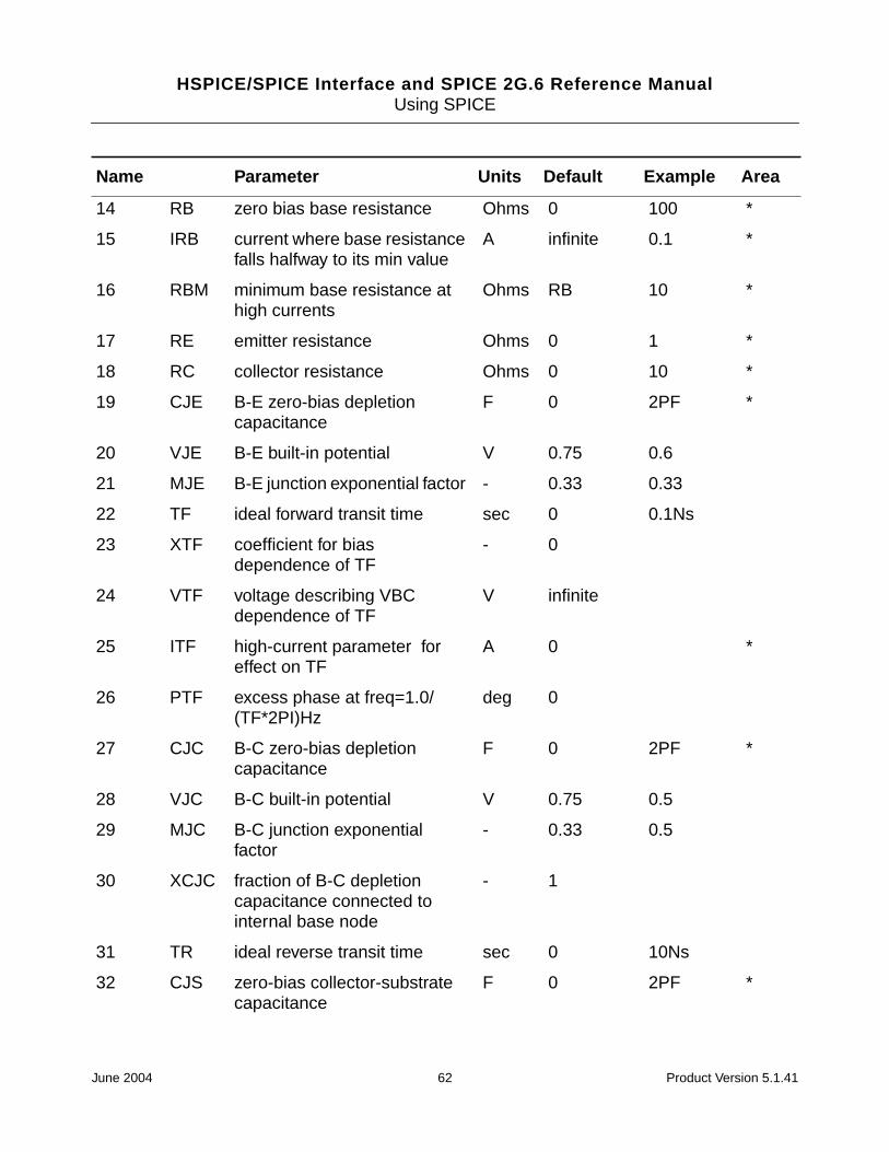
HSPICE/SPICE Interface and SPICE 2G.6 Reference ManualUsing SPICE
14 RB zero bias base resistance Ohms 0 100 *
15 IRB current where base resistancefalls halfway to its min value
A infinite 0.1 *
16 RBM minimum base resistance athigh currents
Ohms RB 10 *
17 RE emitter resistance Ohms 0 1 *
18 RC collector resistance Ohms 0 10 *
19 CJE B-E zero-bias depletioncapacitance
F 0 2PF *
20 VJE B-E built-in potential V 0.75 0.6
21 MJE B-E junction exponential factor - 0.33 0.33
22 TF ideal forward transit time sec 0 0.1Ns
23 XTF coefficient for biasdependence of TF
- 0
24 VTF voltage describing VBCdependence of TF
V infinite
25 ITF high-current parameter foreffect on TF
A 0 *
26 PTF excess phase at freq=1.0/(TF*2PI)Hz
deg 0
27 CJC B-C zero-bias depletioncapacitance
F 0 2PF *
28 VJC B-C built-in potential V 0.75 0.5
29 MJC B-C junction exponentialfactor
- 0.33 0.5
30 XCJC fraction of B-C depletioncapacitance connected tointernal base node
- 1
31 TR ideal reverse transit time sec 0 10Ns
32 CJS zero-bias collector-substratecapacitance
F 0 2PF *
Name Parameter Units Default Example Area
June 2004 62 Product Version 5.1.41

HSPICE/SPICE Interface and SPICE 2G.6 Reference ManualUsing SPICE
NJF and PJF Model Type (JFET Model)
The JFET model is derived from the FET model of Shichman and Hodges. The DCcharacteristics are defined by the parameters VTO and BETA, which determine the variationof drain current with gate voltage; LAMBDA, which determines the output conductance; andIS, the saturation current of the two gate junctions. Two ohmic resistances, RD and RS, areincluded. Charge storage is modeled by nonlinear depletion layer capacitances for both gatejunctions which vary as the -1/2 power of junction voltage and are defined by the parametersCGS, CGD, and PB.
33 VJS substrate junction built-inpotential
V 0.75
34 MJS substrate junction exponentialfactor
- 0 0.5
35 XTB forward and reverse betatemperature exponent
- 0
36 EG energy gap for temperatureeffect on IS
eV 1.11
37 XTI temperature exponent foreffect on IS
- 3
38 KF flicker-noise coefficient - 0
39 AF flicker-noise exponent - 1
40 FC coefficient for forward-biasdepletion capacitance formula
- 0.5
Name Parameter Units Default Example Area
1 VTO threshold voltage V -2.0 -2.0
2 BETA transconductanceparameter
A/V**2 1.0E-4 1.0E-3 *
3 LAMBDA channel lengthmodulation parameter
1/V 0 1.0E-4
4 RD drain ohmic resistance Ohm 0 100 *
5 RS source ohmic resistance Ohm 0 100 *
Name Parameter Units Default Example Area
June 2004 63 Product Version 5.1.41

HSPICE/SPICE Interface and SPICE 2G.6 Reference ManualUsing SPICE
NMOS & PMOS Model Type (MOSFET Model)
SPICE provides three MOSFET device models that differ in the formulation of the I-Vcharacteristic. The variable LEVEL specifies the model to be used:
LEVEL=1 -> Shichman-HodgesLEVEL=2 -> MOS2 (as described in [1])LEVEL=3 -> MOS3, a semi-empirical model (Refer to References information aboutadditional charge relations.)
The DC characteristics of the MOSFET are defined by the device parameters VTO, KP,LAMBDA, PHI, and GAMMA. These parameters are computed by SPICE if processparameters (NSUB, TOX, . . .) are given, but user-specified values always override. VTO ispositive (negative) for enhancement mode and negative (positive) for depletion mode N-channel (P-channel) devices. Charge storage is modeled by three constant capacitors,CGSO, CGDO, and CGBO which represent overlap capacitances, by the nonlinear thin-oxidecapacitance which is distributed among the gate, source, drain, and bulk regions, and by thenonlinear depletion-layer capacitances for both substrate junctions divided into bottom andperiphery, which vary as the MJ and MJSW power of junction voltage respectively, and aredetermined by the parameters CBD, CBS, CJ, CJSW, MJ, MJSW, and PB. There are two built-in models of the charge storage effects associated with the thin-oxide. The default is thepiecewise linear voltage-dependent capacitance model proposed by Meyer. The secondchoice is the charge-controlled capacitance model of Ward and Dutton [1]. The XQC modelparameter acts as a flag and a coefficient at the same time. As the former, it causes theprogram to use Meyer’s model whenever larger than 0.5 or not specified, and the charge-
6 CGS zero-bias G-S junctioncapacitance
F 0 5PF *
7 CGD zero-bias G-D junctioncapacitance
F 0 1PF *
8 PB gate junction potential V 1 0.6
9 IS gate junction saturationcurrent
A 1.0E-14 1.0E-14 *
10 KF flicker noise coefficient - 0
11 AF flicker noise exponent - 1
12 FC coefficient for forward-bias depletioncapacitance formula
- 0.5
Name Parameter Units Default Example Area
June 2004 64 Product Version 5.1.41

HSPICE/SPICE Interface and SPICE 2G.6 Reference ManualUsing SPICE
controlled model when between 0 and 0.5. In the latter case, its value defines the share ofthe channel charge associated with the drain terminal in the saturation region. The thin-oxidecharge storage effects are treated slightly different at the LEVEL=1 model. These voltage-dependent capacitances are included only if TOX is specified in the input description and theyare represented using Meyer’s formulation.
There is some overlap among the parameters describing the junctions; for example, thereverse current can be input either as IS (in A) or as JS (in A/m**2). Whereas the first is anabsolute value, the second is multiplied by AD and AS to give the reverse current of the drainand source junctions, respectively. This methodology has been chosen because there is nosense in relating always junction characteristics with AD and AS entered on the device card;the areas can be defaulted. The same idea applies also to the zero-bias junctioncapacitances CBD and CBS (in F) on one hand, and CJ (in F/m**2) on the other. The parasiticdrain and source series resistance can be expressed as either RD and RS (in ohms) or RSH(in ohms/sq), the latter being multiplied by the number of squares NRD and NRS input on thedevice card.
Name Parameter Units Default Example
1 LEVEL model index - 1
2 VTO zero-bias threshold voltage V 0.0 0.0
3 KP transconductance parameter A/V**2 2.0E-5 3.1E-5
4 GAMMA bulk threshold parameter V**0.5 0.0 0.37
5 PHI surface potential V 0.6 0.65
6 LAMBDA channel-length modulation(MOS1 and MOS2 only)
1/V 0.0 0.02
7 RD drain ohmic resistance Ohm 0.0 1.0
8 RS source ohmic resistance Ohm 0.0 1.0
9 CBD zero-bias B-D junctioncapacitance
F 0.0 20FF
10 CBS zero-bias B-S junctioncapacitance
F 0.0 20FF
11 IS bulk junction saturationcurrent
A 1.0E-14 1.0E-15
12 PB bulk junction potential V 0.8 0.87
13 CGSO gate-source overlapcapacitance per meterchannel width
F/m 0.0 4.0E-11
June 2004 65 Product Version 5.1.41

HSPICE/SPICE Interface and SPICE 2G.6 Reference ManualUsing SPICE
14 CGDO gate-drain overlapcapacitance per meterchannel width
F/m 0.0 4.0E-11
15 CGBO gate-bulk overlapcapacitance per meterchannel length
F/m 0.0 2.0E-10
16 RSH drain and source diffusionsheet resistance
Ohm/sq. 0.0 10.0
17 CJ zero-bias bulk junctionbottom cap. per sq-meter ofjunction area
F/m**2 0.0 2.0E-4
18 MJ bulk junction bottom gradingcoef.
- 0.5 0.5
19 CJSW zero-bias bulk junctionsidewall cap. per meter ofjunction perimeter
F/m 0.0 1.0E-9
20 MJSW bulk junction sidewall gradingcoef.
- 0.33
21 JS bulk junction saturationcurrent persq-meter of junction area
A/m**2 1.0E-8
22 TOX oxide thickness meter 1.0E-7 1.0E-7
23 NSUB substrate doping 1/cm**3 0.0 4.0E15
24 NSS surface state density 1/cm**2 0.0 1.0E10
25 NFS fast surface state density 1/cm**2 0.0 1.0E10
26 TPG type of gate material: +1 opp.to substrate -1 same assubstrate0 A1 gate
- 1.0
27 XJ metallurgical junction depth meter 0.0 1U
28 LD lateral diffusion meter 0.0 0.8U
29 UO surface mobility cm**2/V-s 600 700
Name Parameter Units Default Example
June 2004 66 Product Version 5.1.41
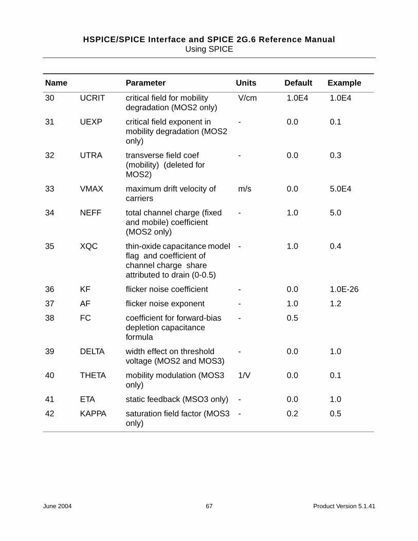
HSPICE/SPICE Interface and SPICE 2G.6 Reference ManualUsing SPICE
30 UCRIT critical field for mobilitydegradation (MOS2 only)
V/cm 1.0E4 1.0E4
31 UEXP critical field exponent inmobility degradation (MOS2only)
- 0.0 0.1
32 UTRA transverse field coef(mobility) (deleted forMOS2)
- 0.0 0.3
33 VMAX maximum drift velocity ofcarriers
m/s 0.0 5.0E4
34 NEFF total channel charge (fixedand mobile) coefficient(MOS2 only)
- 1.0 5.0
35 XQC thin-oxide capacitance modelflag and coefficient ofchannel charge shareattributed to drain (0-0.5)
- 1.0 0.4
36 KF flicker noise coefficient - 0.0 1.0E-26
37 AF flicker noise exponent - 1.0 1.2
38 FC coefficient for forward-biasdepletion capacitanceformula
- 0.5
39 DELTA width effect on thresholdvoltage (MOS2 and MOS3)
- 0.0 1.0
40 THETA mobility modulation (MOS3only)
1/V 0.0 0.1
41 ETA static feedback (MSO3 only) - 0.0 1.0
42 KAPPA saturation field factor (MOS3only)
- 0.2 0.5
Name Parameter Units Default Example
June 2004 67 Product Version 5.1.41

HSPICE/SPICE Interface and SPICE 2G.6 Reference ManualUsing SPICE
Subcircuits
A subcircuit that consists of SPICE elements can be defined and referenced in a fashionsimilar to device models. The subcircuit is defined in the input deck by a grouping of elementcards; the program then automatically inserts the group of elements wherever the subcircuitis referenced. There is no limit on the size or complexity of subcircuits, and subcircuits maycontain other subcircuits. See Example of Data Decks for an example of subcircuit usage.
.SUBCKT Card
General form:
.SUBCKT SUBNAM N1 <N2 N3 . . .>
Examples:
.SUBCKT OPAMP 1 2 3 4
A circuit definition is begun with a .SUBCKT card. SUBNAM is the subcircuit name, and N1,N2, . . . are the external nodes, which cannot be zero. The group of element cards whichimmediately follow the .SUBCKT card define the subcircuit. The last card in a subcircuitdefinition is the .ENDS card (see below). Control cards may not appear within a subcircuitdefinition; however, subcircuit definitions may contain anything else, including other subcircuitdefinitions, device models, and subcircuit calls (see below).
Note: Any device models or subcircuit definitions included as part of a subcircuit definitionare strictly local (that is, such models and definitions are not known outside the subcircuitdefinition). Also, any element nodes not included on the .SUBCKT card are strictly local, withthe exception of 0 (ground) which is always global.
June 2004 68 Product Version 5.1.41
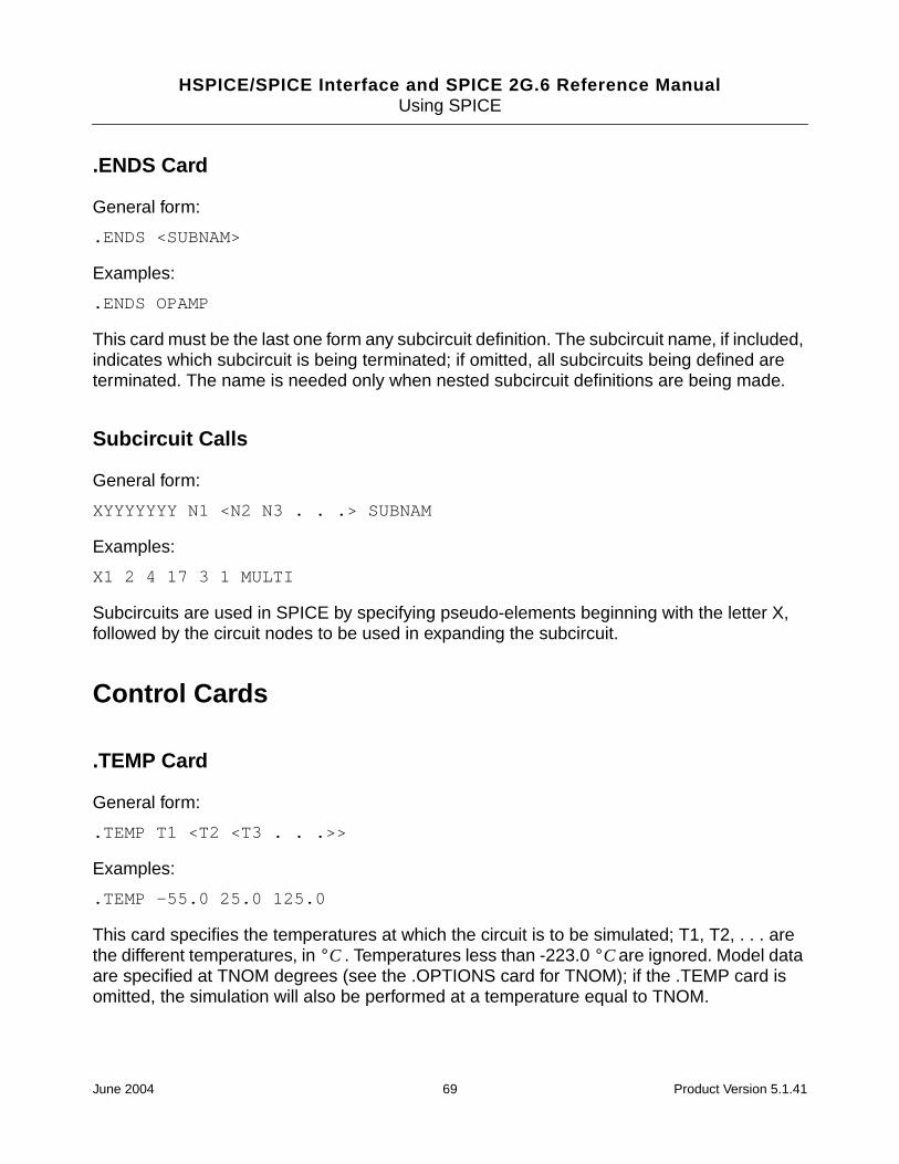
HSPICE/SPICE Interface and SPICE 2G.6 Reference ManualUsing SPICE
.ENDS Card
General form:
.ENDS <SUBNAM>
Examples:
.ENDS OPAMP
This card must be the last one form any subcircuit definition. The subcircuit name, if included,indicates which subcircuit is being terminated; if omitted, all subcircuits being defined areterminated. The name is needed only when nested subcircuit definitions are being made.
Subcircuit Calls
General form:
XYYYYYYY N1 <N2 N3 . . .> SUBNAM
Examples:
X1 2 4 17 3 1 MULTI
Subcircuits are used in SPICE by specifying pseudo-elements beginning with the letter X,followed by the circuit nodes to be used in expanding the subcircuit.
Control Cards
.TEMP Card
General form:
.TEMP T1 <T2 <T3 . . .>>
Examples:
.TEMP -55.0 25.0 125.0
This card specifies the temperatures at which the circuit is to be simulated; T1, T2, . . . arethe different temperatures, in . Temperatures less than -223.0 are ignored. Model dataare specified at TNOM degrees (see the .OPTIONS card for TNOM); if the .TEMP card isomitted, the simulation will also be performed at a temperature equal to TNOM.
°C °C
June 2004 69 Product Version 5.1.41

HSPICE/SPICE Interface and SPICE 2G.6 Reference ManualUsing SPICE
.WIDTH Card
General form:
.WIDTH IN=COLNUM OUT=COLNUM
Examples:
.WIDTH IN =72 OUT=133
This card specifies the last column read from each line of input; the setting takes effect withthe next line read. The default value for COLNUM is 80. The out parameter specifies theoutput print width. Permissible values for the output print width are 80 and 133.
.OPTIONS Card
General form:
.OPTIONS OPT1 OPT2 . . .(or OPT=OPTVAL . . .)
Examples:
.OPTIONS ACCT LIST NODE
This card allows the user to reset program control and user options for specific simulationpurposes. Any combination of the following options may be included, in any order.
Option Effect
ACCT causes accounting and run time statistics to be printed.
LIST causes the summary listing of the input data to be printed.
NOMOD suppresses the printout of the model parameters.
NOPAGE suppresses page ejects.
NODE causes the printing of the node table.
OPTS causes the option values to be printed.
GMIN=x resets the value of GMIN, the minimum conductance allowed by theprogram. The default value is 1.0E-12. x is some positive number.
RELTOL=x resets the relative error tolerance of the program. The default is 0.001(0.1 percent); x is some positive number.
ABSTOL=x resets the absolute current error tolerance of the program. The defaultvalue is 1 picoamp. x is some positive number.
June 2004 70 Product Version 5.1.41

HSPICE/SPICE Interface and SPICE 2G.6 Reference ManualUsing SPICE
VNTOL=x resets the absolute voltage error tolerance of the program. The defaultvalue is 1 microvolt. x is some positive number.
TRTOL=x resets the transient error tolerance. The default value is 7.0. Thisparameter is an estimate of the factor by which SPICE overestimates theactual truncation error. x is some positive number.
CHGTOL=x resets the charge tolerance of the program. The default value is 1.0E-14.x is some positive number.
PIVTOL=x resets the absolute minimum value for a matrix entry to be accepted as apivot. The default value is 1.0E-13. x is some positive number.
PIVREL=x resets the relative ratio between the largest column entry and anacceptable pivot value. The default value is 1.0E-3. In the numericalpivoting algorithm the allowed minimum pivot value is determined by
EPSREL=AMAX1(PIVREL*MAXVAL,PIVTOL)
where MAXVAL is the maximum element in the column where a pivot issought (partial pivoting). x is some positive number.
NUMDGT=x resets the number of significant digits printed for output variable values. Xmust satisfy the relation
0 <x <8
The default value is 4. Note: this option is independent of the errortolerance used by SPICE; that is, if the values of options RELTOL,ABSTOL, etc. are not changed then one may be printing numerical ‘noise’for NUMDGT>4. x is some positive number.
TNOM=x resets the nominal temperature. The default value is 27 deg C (300 degK). x is some positive number.
ITL1=x resets the dc iteration limit. The default is 100. x is some positive number.
ITL2=x resets the dc transfer curve iteration limit. The default is 50; x is somepositive number.
ITL3=x resets the lower transient analysis iteration limit. The default value is 4. xis some positive number.
ITL4=x resets the transient analysis timepoint iteration limit. The default is 10. x issome positive number.
ITL5=x resets the transient analysis total iteration limit. The default is 5000. SetITL5=0 to omit this test. x is some positive number.
Option Effect
June 2004 71 Product Version 5.1.41

HSPICE/SPICE Interface and SPICE 2G.6 Reference ManualUsing SPICE
.OP Card
General form:
ITL6=x resets the dc iteration limit at each of the source stepping method. Thedefault is 0 which means not to use this method.; x is some positivenumber.
CPTIME=x the maximum cpu-time in seconds allowed for this job. x is some positivenumber.
LIMTIM=x resets the amount of cpu time reserved by SPICE for generating plotsshould a cpu time-limit cause job termination. The default value is 2(seconds). x is some positive number.
LIMPTS=x resets the total number of points that can be printed or plotted in a dc, ac,or transient analysis. The default value is 201. x is some positive number.
LVLCOD=x f x is 2 (two), then machine code for the matrix solution will be generated.Otherwise, no machine code is generated. The default is 2. Applies onlyto CDC computers. x is some positive number.
LVLTIM=x is x is 1 (one), the iteration timestep control is used. If x is 2 (two), thetruncation-error timestep is used. The default value is 2. If method=Gearand MAXORD>2 then LVLTIM is set to 2 by SPICE. x is some positivenumber.
METHOD=name sets the numerical integration method used by SPICE. Possible namesare Gear or trapezoidal. The default is trapezoidal. x is some positivenumber.
MAXORD=x sets the maximum order for the integration method if Gear’s variable-order method is used. X must be between 2 and 6. The default is 2. x issome positive number.
DEFL=x resets the value for MOS channel length; the default is 100.0 micrometer.x is some positive number.
DEFW=x resets the value for MOS channel width; the default is 100.0 micrometer. xis some positive number.
DEFAD=x resets the value for MOS drain diffusion area; the default is 0.0. x is somepositive number.
DEFAS=x resets the value for MOS source diffusion area; the default is 0.0. x issome positive number.
Option Effect
June 2004 72 Product Version 5.1.41

HSPICE/SPICE Interface and SPICE 2G.6 Reference ManualUsing SPICE
.OP
The inclusion of this card in an input deck will force SPICE to determine the DC operatingpoint of the circuit with inductors shorted and capacitors opened.
Note: A DC analysis is automatically performed prior to a transient analysis to determine thetransient initial conditions,and prior to an AC small-signal analysis to determine the linearized,small-signal models for nonlinear devices.
SPICE performs a DC operating point analysis if no other analyses are requested.
.DC Card
General form:
.DC SRCNAM VSTART VSTOP VINCR[SRC2 START2 STOP2 INCR2]
Examples:
.DC VIN 0.25 5.0 0.25
.DC VDS 0 10 .5 VGS 0 5 1
.DC VCE 0 10 .25 IB 0 10U 1U
This card defines the DC transfer curve source and sweep limits. SRCNAM is the name of anindependent voltage or current source. VSTART, VSTOP, and VINCR are the starting, final,and incrementing values, respectively. The first example will cause the value of the voltagesource VIN to be swept from 0.25 volts to 5.0 Volts in increments of 0.25 volts. A secondsource (SRC2) may optionally be specified with associated sweep parameters. In this case,the first source will be swept over its range for each value of the second source. This optioncan be useful for obtaining semiconductor device output characteristics. See the secondsample data deck in that section of the guide.
.NODESET Card
General form:
.NODESET V(NODNUM)=VAL V(NODNUM)=VAL . . .
Examples:
NODESET V(12)=4.5 V(4)=2.23
This card helps the program find the DC or initial transient solution by making a preliminarypass with the specified nodes held to the given voltages. The restriction is then released andthe iteration continues to the true solution. The .NODESET card may be necessary forconvergence on bistable or astable circuits. In general, this card should not be necessary.
June 2004 73 Product Version 5.1.41

HSPICE/SPICE Interface and SPICE 2G.6 Reference ManualUsing SPICE
.IC Card
General form:
.IC V(NODNUM)=VAL V(NODNUM)=VAL . . .
Examples:
.IC V(11)=5 V(4)=-5 V(2)=2.2
This card is for setting transient initial conditions. It has two different interpretations,depending on whether the UIC parameter is specified on the .TRAN card. Also, one shouldnot confuse this card with the .NODESET card. The .NODESET card is only to help DCconvergence and does not affect final bias solution (except for multi-stable circuits). The twointerpretations of this card are as follows:
1. When the UIC parameter is specified on the .TRAN card, the node voltages specified onthe .IC card are used to compute the capacitor, diode, BJT, JFET, and MOSFET initialconditions. This is equivalent to specifying the IC=. . . parameter on each device card butis much more convenient. The IC=. . . parameter can still be specified and will takeprecedence over the .IC values. Since no DC bias (initial transient) solution is computedbefore the transient analysis, one should take care to specify all DC source voltages onthe .IC card if they are to be used to compute device initial conditions.
2. When the UIC parameter is not specified on the .TRAN card, the DC bias (initialtransient) solution will be computed before the transient analysis. In this case, the nodevoltages specified on the .IC card will be forced to the desired initial values during thebias solution. During transient analysis, the constraint on these node voltages isremoved.
.TF Card
General form:
.TF OUTVAR INSRC
Examples:
.TF V(5,3) VIN
.TF I(VLOAD) VIN
This card defines the small-signal output and input for the DC small-signal analysis. OUTVARis the small-signal output variable and INSRC is the small-signal input source. If this card isincluded, SPICE will compute the DC small-signal value of the transfer function (output/input),input resistance, and output resistance. For the first example, SPICE would compute the ratioof V(5,3) to VIN, the small-signal input resistance at VIN, and the small-signal output
June 2004 74 Product Version 5.1.41

HSPICE/SPICE Interface and SPICE 2G.6 Reference ManualUsing SPICE
resistance measured across nodes5 and 3.
.SENS Card
General form:
.SENS OV1 <OV2 . . .>
Examples:
.SENS V(9) V(4,3) V(17) I(VCC)
If a .SENS card is included in the input deck, SPICE will determine the DC small-signalsensitivities of each specified output variable with respect to every circuit parameter.
Note: For large circuits, large amounts of output can be generated.
.AC Card
General form:
.AC DEC ND FSTART FSTOP.AC OCT NO FSTART FSTOP.AC LIN NP FSTART FSTOP
Examples:
.AC DEC 10 1 10K
.AC DEC 10 1K 100MEG
.AC LIN 100 1 100HZ
DEC stands for decade variation and ND is the number of points per decade. OCT stands foroctave variation, and NO is the number of points per octave. LIN stands for linear variation,and NP is the number of points. FSTART is the starting frequency, and FSTOP is the finalfrequency. If this card is included in the deck, SPICE will perform an AC analysis of the circuitover the specified frequency range.
Note: In order for this analysis to be meaningful, at least one independent source must havebeen specified with an AC value.
.DISTO Card
General form:
June 2004 75 Product Version 5.1.41

HSPICE/SPICE Interface and SPICE 2G.6 Reference ManualUsing SPICE
.DISTO RLOAD <INTER <SKW2 <REFPWR <SPW2>>>>
Examples:
.DISTO RL 2 0.95 1.0E-3 0.75
This card controls whether SPICE will compute the distortion characteristic of the circuit in asmall-signal mode as a part of the ac small-signal sinusoidal steady-state analysis. Theanalysis is performed assuming that one or two signal frequencies are imposed at the input;let the two frequencies be f1 (the normal analysis frequency) and f2 (=SKW2*f1). Theprogram then computes the following distortion measures:
RLOAD is the name of the output load resistor into which all distortion power products are tobe computed. INTER is the interval at which the summary printout of the contributions of allnonlinear devices to the total distortion is to be printed. If omitted or set to 0, no summaryprintout will be made. REFPWR is the reference power level used in computing the distortionproducts; if omitted, a value of 1 mW (that is, dbm) is used. SKW2 is the ratio of f2 to f1. Ifomitted, a value of 0.9 is used (that is, f2 = 0.9*f1). SPW2 is the amplitude of f2. If omitted, avalue of 1.0 is assumed.
The distortion measures HD2, HD3, SIM2, DIM2, and DIM3 may also be printed and/orplotted. (See the description of the .PRINT and .PLOT cards.)
.NOISE Card
General form:
.NOISE OUTV INSRC NUMS
Examples:
Distortion Measurements
Measurement Description
HD2 The magnitude of the frequency component 2*f1 assuming that f2 isnot present.
HD3 The magnitude of the frequency component 3*f1 assuming that f2 isnot present.
SIM2 The magnitude of the frequency component f1 + f2.
DIM2 The magnitude of the frequency component f1 - f2.
DIM3 The magnitude of the frequency component 2*f1 - f2.
June 2004 76 Product Version 5.1.41

HSPICE/SPICE Interface and SPICE 2G.6 Reference ManualUsing SPICE
.NOISE V(5) VIN 10
This card controls the noise analysis of the circuit. The noise analysis is performed inconjunction with the AC analysis. (See the .AC card.) OUTV is an output voltage that definesthe summing point. INSRC is the name of the independent voltage or current source that isthe noise input reference. NUMS is the summary interval. SPICE will compute the equivalentoutput noise at the specified output as well as the equivalent input noise at the specified input.In addition, the contributions of every noise generator in the circuit will be printed at everyNUMS frequency points (the summary interval). If NUMS is 0, no summary printout will bemade.
The output noise and the equivalent input noise may also be printed and/or plotted. (See thedescription of the .PRINT and .PLOT cards.)
.TRAN Card
General form:
.TRAN TSTEP TSTOP <TSTART <TMAX>> <UIC>
Examples:
.TRAN 1NS 100NS
.TRAN 1NS 1000NS 500NS
.TRAN 10NS 1US UIC
TSTEP is the printing or plotting increment for line-printer output. For use with the post-processor, TSTEP is the suggested computing increment. TSTOP is the final time, andTSTART is the initial time. If TSTART is omitted, it is assumed to be zero. The transientanalysis always begins at time zero. In the interval 0, TSTART>, the circuit is analyzed (toreach a steady state), but no outputs are stored. In the interval <TSTART, TSTOP>, the circuitis analyzed and outputs are stored. TMAX is the maximum stepsize that SPICE will use. (Fordefault, the program chooses either TSTEP or (TSTOP-TSTART)/50.0, whichever is smaller.)TMAX is useful when one wishes to guarantee a computing interval which is smaller than theprinter increment, TSTEP.
UIC (use initial conditions) is an optional keyword that indicates that the user does not wantSPICE to solve for the quiescent operating point before beginning the transient analysis. Ifthis keyword is specified, SPICE uses the values specified using IC=. . . on the variouselements as the initial transient condition and proceeds with the analysis. If the .IC card hasbeen specified, the node voltages on the .IC card are used to compute the initial conditionsfor the devices. Look at the description on the .IC card for its interpretation when UIC is notspecified.
June 2004 77 Product Version 5.1.41

HSPICE/SPICE Interface and SPICE 2G.6 Reference ManualUsing SPICE
.FOUR Card
General form:
.FOUR FREQ OV1 <OV2 OV3 . . .>
Examples:
.FOUR 100K V(5)
This card controls whether SPICE performs a Fourier analysis as a part of the transientanalysis. FREQ is the fundamental frequency, and OV1, . . . are the output variables for whichthe analysis is desired. The Fourier analysis is performed over the interval <TSTOP-period,TSTOP>, where TSTOP is the final time specified for the transient analysis, and period is oneperiod of the fundamental frequency. The DC component and the first nine components aredetermined. For maximum accuracy, TMAX (see the .TRAN card) should be set to period/100.0 (or less for very high-Q circuits).
.PRINT Card
General form:
.PRINT PRTYPE OV1 <OV2 . . . OV8>
Examples:
.PRINT TRAN V(4) I(VIN)
.PRINT AC VM(4,2) VR(7) VP(8,3)
.PRINT DC V(2) I(VSRC) V(23,17)
.PRINT NOISE INOISE
.PRINT DISTO HD3 SIM2(DB)
June 2004 78 Product Version 5.1.41
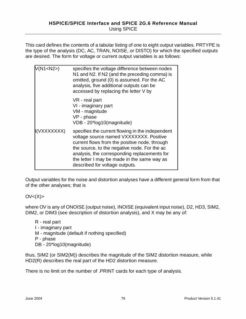
HSPICE/SPICE Interface and SPICE 2G.6 Reference ManualUsing SPICE
This card defines the contents of a tabular listing of one to eight output variables. PRTYPE isthe type of the analysis (DC, AC, TRAN, NOISE, or DISTO) for which the specified outputsare desired. The form for voltage or current output variables is as follows:
Output variables for the noise and distortion analyses have a different general form from thatof the other analyses; that is
OV<(X)>
where OV is any of ONOISE (output noise), INOISE (equivalent input noise), D2, HD3, SIM2,DIM2, or DIM3 (see description of distortion analysis), and X may be any of:
R - real partI - imaginary partM - magnitude (default if nothing specified)P - phaseDB - 20*log10(magnitude)
thus, SIM2 (or SIM2(M)) describes the magnitude of the SIM2 distortion measure, whileHD2(R) describes the real part of the HD2 distortion measure.
There is no limit on the number of .PRINT cards for each type of analysis.
V(N1<N2>) specifies the voltage difference between nodesN1 and N2. If N2 (and the preceding comma) isomitted, ground (0) is assumed. For the ACanalysis, five additional outputs can beaccessed by replacing the letter V by
VR - real partVI - imaginary partVM - magnitudeVP - phaseVDB - 20*log10(magnitude)
I(VXXXXXXX) specifies the current flowing in the independentvoltage source named VXXXXXXX. Positivecurrent flows from the positive node, throughthe source, to the negative node. For the acanalysis, the corresponding replacements forthe letter I may be made in the same way asdescribed for voltage outputs.
June 2004 79 Product Version 5.1.41

HSPICE/SPICE Interface and SPICE 2G.6 Reference ManualUsing SPICE
.PLOT Card
General form:
.PLOT PLTYPE OV1 <(PLO1,PHI1)> <OV2<(PLO2,PHI2)> ... OV8>
Examples:
.PLOT DC V(4) V(5) V(1)
.PLOT TRAN V(17,5) (2,5) I(VIN) V(17) (1,9)
.PLOT AC VM(5) VM(31,24) VDB(5) VP(5)
.PLOT DISTO HD2 HD3(R) SIM2
.PLOT TRAN V(5,3) V(4) (0,5) V(7) (O,10)
This card defines the contents of one plot of from one to eight output variables. PLTYPE isthe type of analysis (DC, AC, TRAN, NOISE, or DISTO) for which the specified outputs aredesired. The syntax for OV1 is identical to that for the .PRINT card, described above.
The optional plot limits (PLO,PHI) may be specified after any of the output variables. All outputvariables to the left of a pair of plot limits (PLO,PHI) will be plotted using the same lower andupper plot bounds. If plot limits are not specified, SPICE will automatically determine theminimum and maximum values of all output variables being plotted and scale the plot to fit.More than one scale will be used if the output variable values warrant (that is, mixing outputvariables with values that are orders-of-magnitude different still gives readable plots).
The overlap of two or more traces on any plot is indicated by the letter X.
When more than one output variable appears on the same plot, the first variable specified willbe printed as well as plotted. If a printout of all variables is desired, then a companion .PRINTcard should be included.
There is no limit on the number of .PLOT cards specified for each type of analysis.
Example of Data Decks
Circuit 1
The following deck determines the DC operating point and small-signal transfer function of asimple differential pair. In addition, the AC small-signal response is computed over thefrequency range 1Hz to 100MHz.
SIMPLE DIFFERENTIAL PAIRVCC 7 0 12VEE 8 0 -12
June 2004 80 Product Version 5.1.41

HSPICE/SPICE Interface and SPICE 2G.6 Reference ManualUsing SPICE
VIN 1 0 AC 1RS1 1 2 1KRS2 6 0 1KQ1 3 2 4 MOD1Q2 5 6 4 MOD1RC1 7 3 10KRC2 7 5 10KRE 4 8 10K.MODEL MOD1 NPN BF=50 VAF=50 IS=1.E-12 RB=100 CJC=.5PF TF=.6NS.TF V(5) VIN.AC DEC 10 1 100MEG.PLOT AC VM(5) VP(5).PRINT AC VM(5) VP(5).END
Circuit 2
The following deck computes the output characteristics of a MOSFET device over the range0-10V for VDS and 0-5V for VGS.
MOS OUTPUT CHARACTERISTICS.OPTIONS NODE NOPAGEVDS 3 0VGS 2 0M1 1 2 0 0 MOD1 L=4U W=6U AD=10P AS=10P.MODEL MOD1 NMOS VTO=-2 NSUB=1.0E15 UO=550*VIDS MEASURES ID, WE COULD HAVE USED VDS, BUT ID WOULD*BE NEGATIVEVIDS 3 1.DC VDS 0 10 .5 VGS 0 5 1.PRINT DC I(VIDS) V(2).PLOT DC I(VIDS).END
Circuit 3
The following deck determines the DC transfer curve and the transient pulse response of asimple RTL inverter. The input is a pulse from 0 to 5 volts with delay, rise, and fall times of 2ns and a pulse width of 30 ns. The transieng20
t interval is 0 to 100 ns, with printing to be done every nanosecond.
SIMPLE RTL INVERTERVCC 4 0 5VIN 1 0 PULSE 0 5 2NS 2NS 2NS 30NS
June 2004 81 Product Version 5.1.41

HSPICE/SPICE Interface and SPICE 2G.6 Reference ManualUsing SPICE
RB 1 2 10KQ1 3 2 0 Q1RC 3 4 1K.PLOT DC V(3).PLOT TRAN V(3)(0,5).PRINT TRAN V(3).MODEL Q1 NPN BF 20 RB 100 TF .1NS CJC 2 PF.DC VIN 0 5 0.1.TRAN 1NS 100NS.END
Circuit 4
The following deck simulates a four-bit binary adder, using several subcircuits to describevarious pieces of the overall circuit.
ADDER - 4 BIT ALL-NAND-GATE BINARY ADDER
***SUBCIRCUIT DEFINITIONS
.SUBCKT NAND 1 2 3 4* NODES: INPUT(2),OUTPUT,VCCQ1 9 5 1 QMODD1CLAMP 0 1 DMODQ2 9 5 2 QMODD2CLAMP 0 2 DMODRB 4 5 4KR1 4 6 1.6KQ3 6 9 8 QMODR2 8 0 1KRC 4 7 130Q4 7 6 10 QMODDVBEDROP 10 3 DMODQ5 3 8 0 QMOD.ENDS NAND
.SUBCKT ONEBIT 1 2 3 4 5 6* NODES: INPUT(2),CARRY-IN,OUTPUT,CARRY-OUT,VCCX1 1 2 7 6 NANDX2 1 7 8 6 NANDX3 2 7 9 6 NANDX4 8 9 10 6 NANDX5 3 10 11 6 NANDX6 3 11 12 6 NANDX7 10 11 13 6 NANDX8 12 13 4 6 NANDX9 11 7 5 6 NAND.ENDS ONEBIT
June 2004 82 Product Version 5.1.41

HSPICE/SPICE Interface and SPICE 2G.6 Reference ManualUsing SPICE
.SUBCKT TWOBIT 1 2 3 4 5 6 7 8 9* NODES: INPUT - BIT0(2)/BIT1(2),OUTPUT - BIT0/BIT1,* CARRY-IN,CARRY-OUT,VCCX1 1 2 7 5 10 9 ONEBITX2 3 4 10 6 8 9 ONEBIT.ENDS TWOBIT
.SUBCKT FOURBIT 1 2 3 4 5 6 7 8 9 10 11 12 13 14 15* NODES: INPUT - BIT0(2)/BIT1(2)/BIT2(2)/BIT3(2),* OUTPUT - BIT0/BIT1/BIT2/BIT3,CARRY-IN,CARRY-OUT,VCCX1 1 2 3 4 9 10 13 16 15 TWOBITX2 5 6 7 8 11 12 16 14 15 TWOBIT.ENDS FOURBIT
*** DEFINE NOMINAL CIRCUIT.MODEL DMOD D.MODEL QMOD NPN(BF=75 RB=100 CJE=1PF CJC=3PF)VCC 99 0 DC 5VVIN1A 1 0 PULSE(0 3 0 10NS 10NS 10NS 50NS)VIN1B 2 0 PULSE(0 3 0 10NS 10NS 20NS 100NS)VIN2A 3 0 PULSE(0 3 0 10NS 10NS 40NS 200NS)VIN2B 4 0 PULSE(0 3 0 10NS 10NS 80NS 400NS)VIN3A 5 0 PULSE(0 3 0 10NS 10NS 160NS 800NS)VIN3B 6 0 PULSE(0 3 0 10NS 10NS 320NS 1600NS)VIN4A 7 0 PULSE(0 3 0 10NS 10NS 640NS 3200NS)VIN4B 8 0 PULSE(0 3 0 10NS 10NS 1280NS 6400NS)X1 1 2 3 4 5 6 7 8 9 10 11 12 0 13 99 FOURBITRBIT0 9 0 1KRBIT1 10 0 1KRBIT2 11 0 1KRBIT3 12 0 1KRCOUT 13 0 1K.PLOT TRAN V(1) V(2) V(3) V(4) V(5) V(6) V(7) V(8).PLOT TRAN V(9) V(10) V(11) V(12) V(13).PRINT TRAN V(1) V(2) V(3) V(4) V(5) V(6) V(7) V(8).PRINT TRAN V(9) V(10) V(11) V(12) V(13)
*** (FOR THOSE WITH MONEY (AND MEMORY) TO BURN).TRAN 1NS 6400NS.OPTIONS ACCT LIST NODE LIMPTS=6401.END
Circuit 5
The following deck simulates a transmission-line inverter. Two transmission-line elements arerequired because two propagation modes are excited. In the case of a coaxial line, the first
June 2004 83 Product Version 5.1.41

HSPICE/SPICE Interface and SPICE 2G.6 Reference ManualUsing SPICE
line (T1) models the inner conductor with respect to the shield, and the second line (T2)models the shield with respect to the outside world.
TRANSMISSION-LINE INVERTERV1 1 0 PULSE(0 1 0 0.1N)R1 1 2 50X1 2 0 0 4 TLINER2 4 0 50.SUBCKT TLINE 1 2 3 4T1 1 2 3 4 Z0=50 TD=1.5NST2 2 0 4 0 Z0=100 TD=1NS.ENDS TLINE.TRAN 0.1NS 20NS.PLOT TRAN V(2) V(4).END
Nonlinear Dependent Sources
SPICE allows circuits to contain dependent sources characterized by any of the fourequations:
i=f(v)
v=f(v)
i=f(i)
v=f(i)
where the functions must be polynomials and the arguments may be multi-dimensional. Thepolynomial functions are specified by a set of coefficients p0,p1, . . ., pn. Both the number ofdimensions and the number of coefficients are arbitrary. The meaning of the coefficientsdepends upon the dimension of the polynomial, as shown in the following examples:
Suppose that the function is one-dimensional (that is, a function of one argument). Then thefunction value fv is determined by the following expression in fa (the function argument):
fv = p0 + (p1*fa) + (p2*fa**2) + (p3*fa**3) + (p4*fa**4)+ (p5*fa**5) + . . .
Suppose now that the function is two-dimensional, with arguments fa and fb. Then thefunction value fv is determined by the following expressions:
fv = p0 + (p1*fa) + (p2*fb) + (p3*fa**2) + (p4*fa*fb) +(p5*fb**2)+ (p6*fa**3) + (p7*fa**2*fb) + (p8*fa*fb**2) + (p9*fb**3) + . . .
June 2004 84 Product Version 5.1.41

HSPICE/SPICE Interface and SPICE 2G.6 Reference ManualUsing SPICE
Consider now the case of a three-dimensional polynomial function with arguments fa, fb, andfc. Then the function value fv is determined by the following expression:
fv = p0 + (p1*fa) + (p2*fb) + (p3*fc) + (p4*fa**2) +(p5*fa*fb)+ (p6*fa*fc) + (p7*fb**2) + (p8*fb*fc) + (p9*fc**2) +(p10*fa**3)+ (p11*fa**2*fb) + (p12*fa**2*fc) + (p13*fa*fb**2)+(p14*fa*fb*fc)+ (p15*fa*fc**2) + (p16*fb**3) + (p17*fb**2*fc) +(p18*fb*fc**2)+ (p19*f**3) + (p20*fa**4) + . . .
Note: If the polynomial is one-dimensional and exactly one coefficient is specified, thenSPICE assumes it to be p1 (and p0 = 0.0), in order to facilitate the input of linear controlledsources.
For all four of the dependent sources described below, the initial condition parameter isdescribed as optional. If not specified, SPICE assumes that 0 the initial condition fordependent sources, is an initial guess’for the value of the controlling variable. The programuses this initial condition to obtain the DC operating point of the circuit. After convergence hasbeen obtained, the program continues iterating to obtain the exact value for the controllingvariable. Hence, to reduce the computational effort for the DC operating point (or if thepolynomial specifies a strong nonlinearity), a value fairly close to the actual controllingvariable should be specified for the initial condition.
Voltage-Controlled Current Sources
General form:
GXXXXXXX N+ N- <POLY(ND)>NC1+NC1- ... P0 <P1 ...> <IC=. .>
Examples:
G1 1 0 5 3 0 0.1MGR 17 3 17 3 0 1M 1.5M IC=2VGMLT 23 17 POLY(2) 3 5 1 2 0 1M 17M 3.5U IC=2.5,1.3
N+ and N- are the positive and negative nodes, respectively. Current flow is from the positivenode, through the source, to the negative node. POLY(ND) only has to be specified if thesource is multi-dimensional (one-dimensional is the default). If specified, ND is the number ofdimensions, which must be positive. NC1+, NC1-,. . . are the positive and negative controllingnodes, respectively. One pair of nodes must be specified for each dimension. P0, P1, P2, . .., Pn are the polynomial coefficients. The (optional) initial condition is the initial guess at thevalue(s) of the controlling voltage(s). If not specified, 0.0 is assumed. The polynomialspecifies the source current as a function of the controlling voltage(s). The second exampleabove describes a current source with value
I = 1E-3*V(17,3)+1.5E-3*V(17,3)**2
June 2004 85 Product Version 5.1.41

HSPICE/SPICE Interface and SPICE 2G.6 Reference ManualUsing SPICE
Note: Because the source nodes are the same as the controlling nodes, this source actuallymodels a nonlinear resistor.
Voltage-Controlled Voltage Sources
General form:
EXXXXXXX N+ N- <POLY(ND)>NC1+NC1- ... P0 <P1 ...><IC=...>
Examples:
E1 3 4 21 17 10.5 2.1 1.75EX 17 0 POLY(3) 13 0 15 0 17 0 0 1 1 1 IC=1.5,2.0,17.35
N+ and N- are the positive and negative nodes, respectively. POLY(ND) only has to bespecified if the source is multi-dimensional (one-dimensional is the default). If specified, NDis the number of dimensions, which must be positive. NC1+, NC1-, . . . are the positive andnegative controlling nodes, respectively. One pair of nodes must be specified for eachdimension. P0,P1,P2,. . .,Pn are the polynomial coefficients. The (optional) initial condition isthe initial guess at the value(s) of the controlling voltage(s). If not specified, 0.0 is assumed.The polynomial specifies the source voltage as a function of the controlling voltage(s). Thesecond example above describes a voltage source with value
V = V(13,0) + V(15,0) + V(17,0)
(in other words, an ideal voltage summer).
Current-Controlled Current Sources
General form:
FXXXXXXX N+ N- <POLY(ND)>VN1 <VN2...> P0 <P1...> <IC=...>
Examples:
F1 12 10 VCC 1MA 1.3MFXFER 13 20 VSENS 0 1
N+ and N- are the positive and negative nodes, respectively. Current flow is from the positivenode, through the source, to the negative node. POLY(ND) only has to be specified if thesource is multi-dimensional (one-dimensional is the default). If specified, ND is the number ofdimensions, which must be positive. VN1, VN2, . . . are the names of the voltage sourcesthrough which the controlling current flows; one name must be specified for each dimension.The direction of positive controlling current flow is from the positive node, through the source,to the negative node of each voltage source. P0,P1,P2,. . .,Pn are the polynomial coefficients.
June 2004 86 Product Version 5.1.41
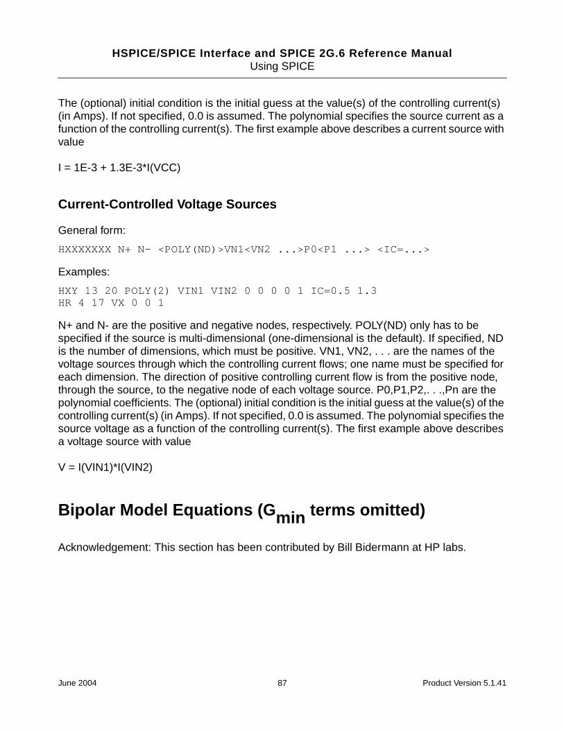
HSPICE/SPICE Interface and SPICE 2G.6 Reference ManualUsing SPICE
The (optional) initial condition is the initial guess at the value(s) of the controlling current(s)(in Amps). If not specified, 0.0 is assumed. The polynomial specifies the source current as afunction of the controlling current(s). The first example above describes a current source withvalue
I = 1E-3 + 1.3E-3*I(VCC)
Current-Controlled Voltage Sources
General form:
HXXXXXXX N+ N- <POLY(ND)>VN1<VN2 ...>P0<P1 ...> <IC=...>
Examples:
HXY 13 20 POLY(2) VIN1 VIN2 0 0 0 0 1 IC=0.5 1.3HR 4 17 VX 0 0 1
N+ and N- are the positive and negative nodes, respectively. POLY(ND) only has to bespecified if the source is multi-dimensional (one-dimensional is the default). If specified, NDis the number of dimensions, which must be positive. VN1, VN2, . . . are the names of thevoltage sources through which the controlling current flows; one name must be specified foreach dimension. The direction of positive controlling current flow is from the positive node,through the source, to the negative node of each voltage source. P0,P1,P2,. . .,Pn are thepolynomial coefficients. The (optional) initial condition is the initial guess at the value(s) of thecontrolling current(s) (in Amps). If not specified, 0.0 is assumed. The polynomial specifies thesource voltage as a function of the controlling current(s). The first example above describesa voltage source with value
V = I(VIN1)*I(VIN2)
Bipolar Model Equations (Gmin terms omitted)
Acknowledgement: This section has been contributed by Bill Bidermann at HP labs.
June 2004 87 Product Version 5.1.41
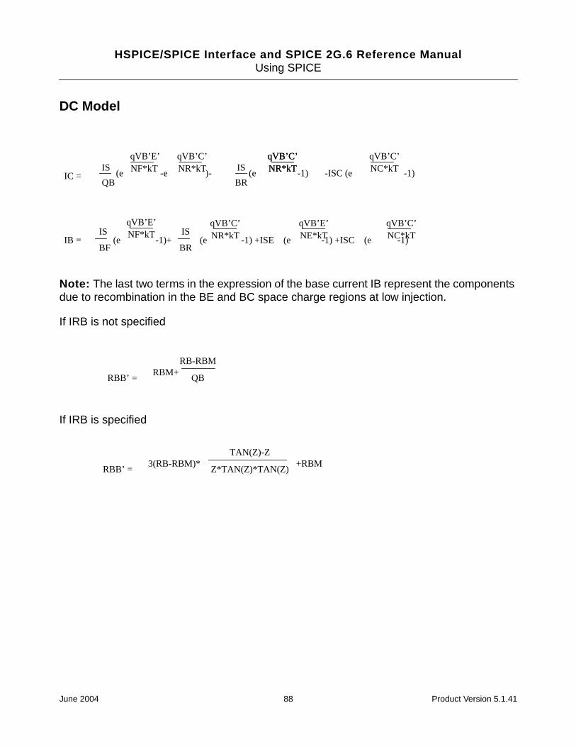
HSPICE/SPICE Interface and SPICE 2G.6 Reference ManualUsing SPICE
DC Model
Note: The last two terms in the expression of the base current IB represent the componentsdue to recombination in the BE and BC space charge regions at low injection.
If IRB is not specified
If IRB is specified
IC =
IB =
IS
QB
IS
BF
(e
(e
)-
-1)+
IS
BR
IS
BR
(e
(e
-1) -ISC (e
-1) +ISE (e -1) +ISC (e -1)
qVB’E’NF*kT
qVB’C’NR*kT-e
qVB’C’NR*kT
qVB’C’NC*kT -1)
qVB’C’NR*kT
qVB’C’NR*kT
qVB’E’NE*kT
qVB’E’NF*kT
qVB’C’NC*kT
RBB’ =RBM+
RB-RBM
QB
RBB’ =3(RB-RBM)*
TAN(Z)-Z
Z*TAN(Z)*TAN(Z)+RBM
June 2004 88 Product Version 5.1.41
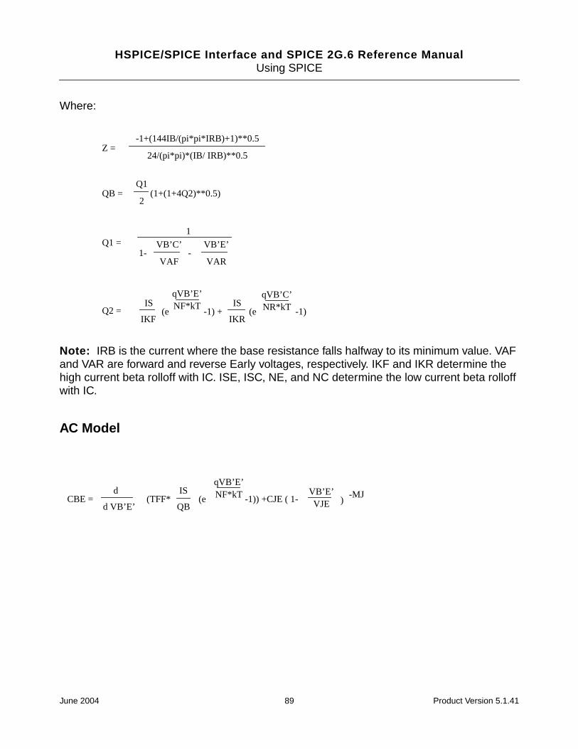
HSPICE/SPICE Interface and SPICE 2G.6 Reference ManualUsing SPICE
Where:
Note: IRB is the current where the base resistance falls halfway to its minimum value. VAFand VAR are forward and reverse Early voltages, respectively. IKF and IKR determine thehigh current beta rolloff with IC. ISE, ISC, NE, and NC determine the low current beta rolloffwith IC.
AC Model
-1+(144IB/(pi*pi*IRB)+1)**0.5
24/(pi*pi)*(IB/ IRB)**0.5Z =
Q1
2QB =
VB’C’
VAF
Q1 =
Q2 =
(1+(1+4Q2)**0.5)
VB’E’
VAR-1-
1
IS
IKF(e -1) +
IS
IKR (e -1)
qVB’C’NR*kT
qVB’E’NF*kT
CBE = d
d VB’E’ (TFF*
IS
QB(e -1)) +CJE ( 1-
qVB’E’NF*kT VB’E’
VJE )-MJ
June 2004 89 Product Version 5.1.41

HSPICE/SPICE Interface and SPICE 2G.6 Reference ManualUsing SPICE
Where:
TFF = TF (1 XTF * (IF/ (IF+ITF)) 2 *e
VB’C’1.44VTF )
IF = IS (e -1)
qVB’E’NF*kT
CB1 = CBC*(1-XCJC)
CB2 = CBC * XCJC
CBC = TR ( e
qVB’C’
kT) +CJC ( 1-
VB’C’VJC
qISNR*kT
)-MJC
CSS = CJS (1-VC’S’VJS
)-MJC
NOTE: all junction capacitances of the form C0*(1-V
phi)
-M
revert to the form
C0/ ((1-FC)**M) * (1 +M*(V-FC*phi)
phi(1-FC)
when V > FC*phi (For CSS assumes FC = 0)
)
June 2004 90 Product Version 5.1.41

HSPICE/SPICE Interface and SPICE 2G.6 Reference ManualUsing SPICE
Noise Model
Temperature Effects
All junctions have dependences identical to the diode model but all N factors are consideredequal 1.
KF*IB**AFf DELTA f
IRBB’4kT
RBB’2
= DELTA f
IRC4kTRC
2= DELTA f
IRE4kTRE
2= DELTA f
IBN = 2qIB DELTA f+2
Note: The first term is shot noise and the second term is flicker noise.
ICN = 2qIC DELTA f2
Note: This is shot noise.
Thermal noise
BF and BR go as (T
TNOM)
XTB
June 2004 91 Product Version 5.1.41

HSPICE/SPICE Interface and SPICE 2G.6 Reference ManualUsing SPICE
when NF=1. This is done through appropriate changes in BF,BR and ISE,ISC according tothe following equations, respectively:
Excess Phase
This is a delay (linear phase) in the gm generator in AC analysis. It is also used in transientanalysis using a Bessel polynomial approximation. Excess phase, PTF, is specified as thenumber of extra degrees of phase at the frequency
Alter Statement and the Source-Stepping Method
The ALTER statement allows SPICE to run with altered circuit parameters.
General form:
.ALTERELEMENT CARDS (DEVICE CARDS, MODEL CARDS).ALTER (or .END CARD)
Examples:
R1 1 0 5KVCC 3 0 10M1 3 2 0 MOD1 L=5U W=2U
BF (or BR’) = BF (or BR)*(T
TNOM) XTB
ISE1 (or ISC’) = ISE (or ISC)*(T
TNOMXTI-XTB)) *e
qEGNk
T-TNOMT*TNOM
f =1
2piTF Hertz
June 2004 92 Product Version 5.1.41

HSPICE/SPICE Interface and SPICE 2G.6 Reference ManualUsing SPICE
.MODEL MOD1 NMOS(VTO=1.0 KP=2.0E-5 PHI=0.6 NSUB=2.0E15 TOX=0.1U)
.ALTERR1 1 0 3.5KVCC 3 0 12M1 3 2 0 MOD1 L=10U W=2U.MODEL MOD1 NMOS(VTO=1.2 KP=2.0E-5 PHI=0.6 NSUB=5.0E15 TOX=1.5U).ALTERM1 3 2 0 MOD1 L=10U W=4U.END
This card introduces the elements, devices and models whose parameters are changedduring the execution of the input deck. The analyses specified in the deck will start over againwith the changed parameters. The .ALTER card with the cards defining the new parametersshould be placed just before the .END card. The syntax for the element (device, model) cardsis identical to that of the cards with the original parameters.
There is no limit on the number of .ALTER cards and the circuit will be re-analyzed as manytimes as the number of .ALTER cards. Subsequent ALTER operations employ parameters ofthe previous change. No topological change of the circuit is allowed.
The source-stepping method can enhance DC convergence, but it is slower than direct useof the Newton-Raphson method. Therefore, it is best used as an alternative to achieveconvergence of DC operating point when the circuit fails to converge by using the Newton-Raphson method. The source-stepping method is used by SPICE when the variable ITL6 inthe .OPTIONS card is set to the iteration limit at each step of the sources.
For example,
.OPTIONS ITL6=30
will cause SPICE to use the source-stepping method with iteration limit 30 at each step. Bydefault, ITL6 is 0, which means to use the Newton-Raphson method directly.
References
[1] A. Vladimirescu and S. Liu, “The Simulation of MOS Integrated Circuits Using SPICE2,”ERL Memo No. ERL M80/7, Electronics Research Laboratory, University of California,Berkeley, Oct. 1980.
June 2004 93 Product Version 5.1.41

HSPICE/SPICE Interface and SPICE 2G.6 Reference ManualUsing SPICE
June 2004 94 Product Version 5.1.41

HSPICE/SPICE Interface and SPICE 2G.6 Reference Manual
Index
AALTER statement, SPICE 92analysis type codes, HSPICE 20analysis type, SPICE
AC small-signal 43DC analysis 42different temperatures 44transient 43
Bbipolar model equations 87
Ccircuit simulation interfaces 9commands, create new run 11control cards, SPICE 69create new run command 11
Ddata deck examples, SPICE 80DC convergence, SPICE 45
Eelement cards, SPICE 48elements, HSPICE/SPICE 26
Ffiles
HSPICEcontrol 21hspice.inp 21hspice.sim 21si.log 22si.out 22waves 22
SPICEcontrol 12netlist 13, 14spice.inp 13spice.sim 13
formatting functions 36element format 36model format 39
HHSPICE
primitive cell requirements 23
Iindependent sources, SPICE 52input format, SPICE 45
Llibrary cells 26linear dependent sources, SPICE 50
Mmodel and element parameters 27
Nnetlisting
HSPICEhierarchical 22name mapping 23netlisting properties 23
variablessimNetlistHier 21
June 2004 95 Product Version 5.1.41
HSPICE/SPICE Interface and SPICE 2G.6 Reference Manual
Pproperties, HSPICE
netlisting 23
Ssemiconductor devices, SPICE
element cards 56model cards 59specifying initial conditions 56
simulation models 27simulation run example, SPICE 11source-stepping method, SPICE 92subcircuits 68
Vvariables, HSPICE
simHost 22
Wwaveform, SPICE 11
June 2004 96 Product Version 5.1.41