HP5432 Microwave Frequency Counter
365
TM 11-6625-3014-14 TECHNICAL MANUAL OPERATOR’S,ORGANIZATIONAL, DIRECT SUPPORT, AND GENERAL SUPPORT MAINTENANCE MANUAL F O R MICROWAVE FREQUENCY COUNTER TD-1225A(V)1/U (NSN 625-01-103-2958) HEADQUARTERS, DEPARTMENT OF THE ARMY SEPTEMBER 1981 Digital Reprint Copyright © 2002 GovTechMedia.com
-
Upload
rob-sullivan -
Category
Documents
-
view
327 -
download
9
Transcript of HP5432 Microwave Frequency Counter

8/21/2019 HP5432 Microwave Frequency Counter
http://slidepdf.com/reader/full/hp5432-microwave-frequency-counter 1/364
T M 1 1 - 6 6 2 5 - 3 0 1 4 - 1 4
T E C H N I C A L M A N U A L
O P E R A T O R ’ S , O R G A N I Z A T I O N A L ,
D I R E C T S U P P O R T , A N D G E N E R A L S U P P O R T
M A I N T E N A N C E M A N U A L
F O R
M I C R O W A V E F R E Q U E N C Y C O U N T E R
T D - 1 2 2 5 A ( V ) 1 / U
( N S N 6 2 5 - 0 1 - 1 0 3 - 2 9 5 8 )
H E A D Q U A R T E R S , D E P A R T M E N T O F T H E A R M Y
S E P T E M B E R 1 9 8 1
Digital Reprint Copyright © 2002 GovTechMedia.com

8/21/2019 HP5432 Microwave Frequency Counter
http://slidepdf.com/reader/full/hp5432-microwave-frequency-counter 2/364
SAFETY STEPS
I S THE VI CTI M
TO FOLLOWI F
OF ELECTRI CAL
SOMEONE
SHOCK
DO NOT TRY TO PULL OR GRAB THE I NDI VI DUAL
I F POSSI BLE , TURN OFF THE ELECTRI CAL POWER
I F YOU CANNOT TURN OFF THE ELECTRI CAL
POWER, PULL, PUSH, OR LI FT THE PERSON TO
SAFETY USI NG A WOODEN POLE OR A ROPE OR
SOME OTHER I NSULATI NG MATERI AL
SEND FOR HELP AS SOON AS POSSI BLE
AFTER THE I NJ URED PERSON I S FREE OF
CONTACT WI TH THE SOURCE OF ELECTRI CAL
SHOCK, MOVE THE PERSON A SHORT DI STANCE
AWAY AND I MMEDI ATELY START ARTI FI CI AL
RESUSCI TATI ON
SAFETY
Thi s product has been des i gned and tes te d accordi ng t o I nternati onal Saf et y Requi rements. To ensure
saf e operat i on and to keep the product s af e, the i nformati on, cauti ons, and warni ngs i n thi s manual
must be heeded. Ref er t o Secti on I f or general saf ety consi derati ons appl i cabl e to t hi s product.

8/21/2019 HP5432 Microwave Frequency Counter
http://slidepdf.com/reader/full/hp5432-microwave-frequency-counter 3/364
This manual includes copyright material reproduced by permission of the HEWLETT-PACKARD Company.
TM 11-6625-3014-14
TECHNICAL MANUAL H E A D Q U A R T E R S
D E P A R T M E N T O F T H E A R M Y
NO. 11-6625-3014-14 Washington, D.C. 10 September 1981
O P E R A T O R ’ S , O R G A N I Z A T I O N A L ,
DIRECT SUPPORT, AND GENERAL SUPPORT
M A I N T E N A N C E M A N U A L
M I C R O W A V E F R E Q U E N C Y C O U N T E R
T D - 1 2 2 5 A ( V ) 1 / U
( N S N 6 6 2 5 - 0 1 - 1 0 3 - 2 9 5 8 )
REPORTING OF ERRORS
You can improve this manual by recommending improvements using DA Form 2028-2 located
in the back of the manual. Simply tear out the self-addressed form, fill it out as shown on the sam-ple, fold it where shown, and drop it in the mail.
If there are no blank DA Forms 2028-2 in the back of your manual, use the standard DA Form2028 (Recommended Changes to Publications and Blank Forms) and forward to Commander, US
Army Communications and Electronics Materiel Readiness Command, ATTN: DRSEL-ME-MQ,Fort Monmouth, NJ 07703.
In either case a reply will be forwarded direct to you.
TABLE OF CONTENTS
Section Title Page
0 I N S T R U C T I O N S . . . . . . . . . . . . . . . . . . . . . . 0 - 1
0- 1
0-2
0 - 3
0- 4
0-5
0-6
Scope . . . . . . . . . . . . . . . . . . . ...0-1
Indexes of publications . . . . . . . . . . . . . . 0-1
Forms and records . . . . . . . . . . . . . . . .. 0-1
Reporting of equipment improvement
recommendations (EIR) . . . . . . . . . . . . 0-1
Administrative storage . . . . . . . . . . . . . . 0-1
D e s t r u c t i o n o f a r m y e l e c t r o n i c s m a t e r i e l . . . . . 0 - 1
SERIAL PREFIX: 1840A
This manual applies to Serial Prefix 1840A, unless
accompanied by a Manual Change Sheet indicating
otherwise.
This manual is an authentiation of the manufacturer’s commercial literature which,through usage, has been found to cover thedata required to operate and maintain this equipment. Since the manual was not prepared in accordance with military specificationsand AR 310-3, the format has not been structured to consider levels of maintenance.
i

8/21/2019 HP5432 Microwave Frequency Counter
http://slidepdf.com/reader/full/hp5432-microwave-frequency-counter 4/364
Model 5342ATable of Contents
TABLE OF CONTENTS (Continued)
Section
I
II
III
ii
Title Page
GENERAL INFORMATION . . . . . . . . . . . . . . . . . . . . . . . . . . . . . . . . . . . . . . . 1-11-1. Introduction . . . . . . . . . . . . . . . . . . . . . . . . . . . . . . . . . . . . . . . . . . . . . . . . 1-1
1-3. Specifications . . . . . . . . . . . . . . . . . . . . . . . . . . . . . . . . . . . . . . . . . 1-11-5. Safety Considerations . . . . . . . . . . . . . . . . . . . . . . . . . . . . . . . . . . . . . . . . 1-31-7. Instrument Identification . . . . . . . . . . . . . . . . . . . . . . . . . . . . . . . . . . . . . 1-31-9. Accessories . . . . . . . . . . . . . . . . . . . . . . . . . . . . . . . . . . . . . . . . . . . . . . . . . 1-31-11. Description . . . . . . . . . . . . . . . . . . . . . . . . . . . . . . . . . . . . . . . . . . . . . . . . . . 1-41-13. Options . . . . . . . . . . . . . . . . . . . . . . . . . . . . . . . . . . . . . . . . . . . . . . . . . . . . 1-41-15. Service Equipment Available . . . . . . . . . . . . . . . . . . . . . . . . . . . . . . . . . 1-41-17. Recommended Test Equipment . . . . . . . . . . . . . . . . . . . . . . . . . . . . . . . 1-4
IN ST AL LA TI ON . . . . . . . . . . . . . . . . . . . . . . . . . . . . . . . . . . . . . . . . . . . . . . . . 2-1
2-1. Introduction . . . . . . . . . . . . . . . . . . . . . . . . . . . . . . . . . . . . . . . . . . . . . . . . 2-1
2-3. Unpacking and Inspection . . . . . . . . . . . . . . . . . . . . . . . . . . . . . . . . . . . 2-1
2-5. Installation Requirements . . . . . . . . . . . . . . . . . . . . . . . . . . . . . . . . . . . . 2-1
2-9. Power Cable . . . . . . . . . . . . . . . . . . . . . . . . . . . . . . . . . . . . . . . . . . . . 2-22-11. Operating Environment . . . . . . . . . . . . . . . . . . . . . . . . . . . . . . . . . . 2-3
2-15. Storage and Shipment . . . . . . . . . . . . . . . . . . . . . . . . . . . . . . . . . . . . . . . 2-32-16. Environment . . . . . . . . . . . . . . . . . . . . . . . . . . . . . . . . . 2-32-19. Packaging . . . . . . . . . . . . . . . . . . . . . . . . . . . . . . . . . . . . . . . . . . . . . . 2-32-22. Field Installation of Options . . . . . . . . . . . . . . . . . . . . . . . . . . . . . . . . . . 2-32-24. Part Numbers for Ordering Option Kits . . . . . . . . . . . . . . . . . . . 2-42-26. Installation of 10 MHz Oscillator Option 001 . . . . . . . . . . . . . . . 2-42-28. Installation of Amplitude Measurement Option 002 2-4. . . . . . . .2-30. Installation of Extended Dynamic Range Option 003 . . . . . . . . 2-72-32. Installation of Digital-to-Analog Conversion
(DAC) Option 004 . . . . . . . . . . . . . . . . . . . . . . . . . . . . . 2-72-34. Installation of HP-IB Option 011 . . . . . . . . . . . . . . . . . . . . . ... 2-8
2-36. HP-IB Interconnections . . . . . . . . . . . . . . . . . . . . . . . . . . . . . . . . . . 2-92-39. 5342A Listen Address . . . . . . . . . . . . . . . . . . . . . . . . . . . . . . . . . . . . 2-92-41. HP-IB Descriptions . . . . . . . . . . . . . . . . . . . . . . . . . . . . . . . . . . . . . . 2-9
OPERATION . . . . . . . . . . . . . . . . . . . . . . . . . . . . . . . . . . . . . . . . . . . . . . . . . . . . . . 3-1
3-1. Introduction . . . . . . . . . . . . . . . . . . . . . . . . . . . . . . . . . . . . . . . . . . . . . . . . 3-1
3-3. Operating Characteristics . . . . . . . . . . . . . . . . . . . . . . . . . . . . . . 3-1
3-5. Operating Ranges . . . . . . . . . . . . . . . . . . . . . . . . . . . . . . . . . . . . . . . 3-1
3-7. Resolution Keys . . . . . . . . . . . . . . . . . . . . . . . . . . . . . . . . . . . . . . . . . 3-1
3-10. CHECK, DAC, and ENTER Keys . . . . . . . . . . . . . . . . . . . . . . . . . . . 3-23-12. FREQ Keys . . . . . . . . . . . . . . . . . . . . . . . . . . . . . . . . . . . . . . . . . . . . . . 3-23-14. Automatic Mode . . . . . . . . . . . . . . . . . . . . . . . . . . . . . . . . . . . . . . . . 3-23-16. Manual Mode . . . . . . . . . . . . . . . . . . . . . . . . . . . . . . . . . . . . . . . . . . 3-2
3-18. Offset Frequencies . . . . . . . . . . . . . . . . . . . . . . . . . . . . . . . . . . . . . . 3-23-20. Amplitude and Offset Measurements . . . . . . . . . . . . . . . . . . . . . 3-23-22. Digital-to-Analog Converter (DAC) Operation . . . . . . . . . . . . . 3-23-24. SET, RESET, RECALL, and CHS Keys 3-2. . . . . . . . . . . . . . . . . . . . . . .3-25. SAMPLE RATE, GATE, and REMOTE . . . . . . . . . . . . . . . . . . . . . . . 3-23-30. AM Tolerance . . . . . . . . . . . . . . . . . . . . . . . . . . . . . . . . . . . . . . . . . . 3-33-32. FM Tolerance . . . . . . . . . . . . . . . . . . . . . . . . . . . . . . . . . . . . . . . . . . . 3-33-34. Automatic Amplitude Discrimination . . . . . . . . . . . . . . . . . . . . . . 3-33-36. Maximum Input Signal Power . . . . . . . . . . . . . . . . . . . . . . . . . . . . . . . . 3-33-39. Input Cable Considerations . . . . . . . . . . . . . . . . . . . . . . . . . . . . 3-4

8/21/2019 HP5432 Microwave Frequency Counter
http://slidepdf.com/reader/full/hp5432-microwave-frequency-counter 5/364
Model 5342ATable of Contents
TABLE OF CONTENTS (Continued)
Section Title Page
III OPERATION (Continued)
3-41. Controls, Indicators, and Connectors . . . . . . . . . . . . . . . . . . . . . . . . . 3-43-43. Operating Procedures . . . . . . . . . . . . . . . . . . . . . . . . . . . . . . . . . . . . . . . 3-4
3-45. Operator Key board Check . . . . . . . . . . . . . . . . . . . . . . . . . . . . . . . . . . . 3-143-47. Error Code Displays . . . . . . . . . . . . . . . . . . . . . . . . . . . . . . . . . . . . . . . . . 3-163-49. Instrument Error Displays . . . . . . . . . . . . . . . . . . . . . . . . . . . . . . . . 3-163-51. Operator Error Displays . . . . . . . . . . . . . . . . . . . . . . . . . . . . . . . . . . 3-173-53. Limit Errors and Sequence Errors . . . . . . . . . . . . . . . . . . . . . . . . . 3-183-57. Options . . . . . . . . . . . . . . . . . . . . . . . . . . . . . . . . . . . . . . . . . . . . . . . . . . . . 3-183-59. Time Base Option 001 . . . . . . . . . . . . . . . . . . . . . . . . . . . . . . . . . . . . . . . 3-183-61. Amplitude Option 002 . . . . . . . . . . . . . . . . . . . . . . . . . . . . . .. 3-183-63. Extended Dynamic Range Option 003 . . . . . . . . . . . . . . . . . . . . . 3-183-65. HP-IB Interface Option 011 . . . . . . . . . . . . . . . . . . . . . . . . . . . . . . 3-183-67. Digital-to-Analog Converter (DAC) Option 004 . . . . . . . . 3-193-69. HP-lB Programming (Option 011) . . . . . . . . . . . . . . . . . . . . . . . . . . . . . 3-193-79. 9825A Program Examples . . . . . . . . . . . . . . . . . . . . . . . . . . . . . . . . . . . . . 3-25
3-81. HP-lB Programming Notes . . . . . . . . . . . . . . . . . . . . . . . . . . . . . . . . . . . 3-283-83. Remote Programming of Diagnostic Mode 6(Option 002,011 Only) . . . . . . . . . . . . . . . . . . . . . . . . . . . . . . 3-30
IV PERFORMANCE TESTS . . . . . . . . . . . . . . . . . . . . . . . . . . . . . . . . . . . . . . . . . . . . . 4-14-1.4-3.4-5.
4-7.4-9.4-11.4-12.4-13.
4-14.
4-15.
4-16.
4-17.
4-18.4-19.4-27.4-28.
4-29.
4-30.4-31.
4-32.4-33.4-34.4-35.
Introduction . . . . . . . . . . . . . . . . . . . . . . . . . . . . . . . . . . . . . . . . . . . . . . . . 4-1
Operational Verification . . . . . . . . . . . . . . . . . . . . . . . . . . . . . . . . . . . . . 4-1Complete Performance Test . . . . . . . . . . . . . . . . . . . . . . . . . . . . . . . . . . 4-1
Equipment Required . . . . . . . . . . . . . . . . . . . . . . . . . . . . . . . . . . . . . . . . 4-1
Test Record . . . . . . . . . . . . . . . . . . . . . . . . . . . . . . . . . . . . . . . . . . . . . . . . . 4-1
Operational Verification Procedures . . . . . . . . . . . . . . . . . . . . . . . . . . 4-2Self-Check . . . . . . . . . . . . . . . . . . . . . . . . . . . . . . . . . . . . . . . . . . . . . . 4-210 Hz—500 MHz Input Sensitivity Test,
(Standard and Option 003 1nstruments Only) . . . . . . . . . . . 4-210 Hz—500 MHz Input Minimum Level and
Amplitude Accuracy Test (Option 002) . . . . . . . . . . . . . . . . 4-310 Hz—500 MHz Input Maximum
Input Test (Option 002) . . . . . . . . . . . . . . . . . . . . . . . . . . . . . . 4-4500 MHz-18 GHz Input Sensitivity Test (Standard and
Option 003 Instruments Only) . . . . . . . . . . . . . . . . . . . . . . . . 4-5500 MHz—18 GHz Input Minimum Level and Amplitude
Accuracy Test (Option 002) . . . . . . . . . . . . . . . . . . . . . . . . . . . 4-6500 MHz-18 GHz High Level Test . . . . . . . . . . . . . . . . . . . . . . . . 4-7
Option 011 HP-IB Verification Program . . . . . . . . . . . . . . . . . . . . . . . . 4-7Digital-to-Analog Converter (DAC) Output Test (Option 004) . . . 4-16Performance Test Procedures . . . . . . . . . . . . . . . . . . . . . . . . . . . . . . . . . 4-17
10 Hz—500 MHz Input Sensitivity Test,(Standard and Option 003 Instruments Only) . . . . . . . . . . . 4-17
10 Hz—500 MHz Input Sensitivity Test, 1 . . . . . . . . . . . . . . 4-18500 MHz—18 GHz Input Sensitivity Test (Standard and
Option 003 Instruments Only) 4-19500 MHz-18 GHz lnput SWR Test . . . . . . . . . . . . . . . . . . . . . . 4-20500 MHz-18 GHz Maximum Input Test . . . . . . . . . . . . . . . . . . . 4-22FM Tolerance Test . . . . . . . . . . . . . . . . . . . . . . . . . . . . . . 4-24Automatic Amplitude Discrimination Test . . . . . . . . . . . . . . . . . 4-26
ii i

8/21/2019 HP5432 Microwave Frequency Counter
http://slidepdf.com/reader/full/hp5432-microwave-frequency-counter 6/364
Model 5342ATable of Contents
Section
IV
V
VI
VI I
V l l l
iv
TABLE OF CONTENTS (Continued)
Title Page
PERFORMANCE TESTS (Continued)
4-36. 500 MHz—18 GHz Input Minimum Level and AmplitudeAccuracy Test (Option 002) . . . . . . . . . . . . . . . . . . . . . . . . . . . 4-27
4-37. 10 Hz—500 MHz Input Minimum Level andAmplitude Accuracy Test (Option 002) . . . . . . . . . . . . . . . . 4-28
4-38. 10 Hz—500 MHz Input MaximumInput Test (Option 002) . . . . . . . . . . . . . . . . . . . . . . . . . . . . . . 4-29
4-39. 10 Hz—500 MHz Input SWR Test (Option 002) . . . . . . . 4-304-40. Digital-to-Analog Converter (DAC) Output
Test (Option 004) . . . . . . . . . . . . . . . . . . . . . . . . . . . . . . . . . . . . 4-31
ADJUSTMENTS . . . . . . . . . . . . . . . . . . . . . . . . . . . . . . . . . . . . . . . . . . . . . . . . . . . . 5-1
5-1. Introduction . . . . . . . . . . . . . . . . . . . . . . . . . . . . . . . . . . . . . . . . . . . . . . . . 5-15-4. Equipment Required . . . . . . . . . . . . . . . . . . . . . . . . . . . . . . . . . . . . . . . . 5-1
5-6. Factory Selected Components . . . . . . . . . . . . . . . . . . . . . . . . . . . . 5-1
5-8. Adjustment Locations . . . . . . . . . . . . . . . . . . . . . . . . . . . . . . . . . . . 5-15-10. Safety Considerations . . . . . . . . . . . . . . . . . . . . . . . . . . . . . . . . . . . . . . . . 5-1
5-12. Adjustment Procedures . . . . . . . . . . . . . . . . . . . . . . . . . . . . . . . . . . . . . . 5-35-13. Power Supply Adjustments . . . . . . . . . . . . . . . . . . . . . . . . . . . . . . 5-35-17. Main Synthesizer Adjustment . . . . . . . . . . . . . . . . . . . . . . . . . . . . 5-45-19. Offset Synthesizer Adjustments . . . . . . . . . . . . . . . . . . . . . . . . . . . 5-5
5-21. IF Adjustment . . . . . . . . . . . . . . . . . . . . . . . . . . . . . . . . . . . . . . . . . . . .5-28. Direct Count Adjustment . . . . . . . . . . . . . . . . . . . . . . . . . . . .5-30. Oscillator Adjustments . . . . . . . . . . . . . . . . . . . . . . . . . . . . . . . . . . . . . . . 5-85-31. A24 Standard Oscillator . . . . . . . . . . . . . . . . . . . . . . . . . . . . . . . . . . 5-85-32. Option 001 Oven Oscillator (10544A) . . . . . . . . . . . . . . . . . . . . . . 5-95-33. Option 002 Amplitude Measurement Adjustments . . . . . . . . . . . . . 5-10
5-34. A16 Adjustments . . . . . . . . . . . . . . . . . . . . . . . . . . . . . . . . . . . . . . . . 5-10
5-38. A27 Adjustments (Resistors A27R9,A27R10) . . . . . . . . . . . . . . . . 5-115-39. Option 002/003 Adjustments . . . . . . . . . . . . . . . . . . . . . . . . . . . . . . . . . 5-12
5-40. A11, A25 Adjustments (Resistors A11R14, A25R31) . . . . . . . . . . 5-12
5-41. Option 004 Digital-to-Analog (DAC) Adjustments . . . . . . . . . . . . . . 5-13
REPLACEABLE PARTS . . . . . . . . . . . . . . . . . . . . . . . . . . . . . . . . . . . . . . . . . . . . . . 6-1
6-1. Introduction . . . . . . . . . . . . . . . . . . . . . . . . . . . . . . . . . . . . . . . . . . . . . . . . 6-16-3. Exchange Assemblies . . . . . . . . . . . . . . . . . . . . . . . . . . . . . . . . . . . . . . . . 6-16-5. Abbreviations and Reference Designations . . . . . . . . . . . . . . . . . . . . 6-1
6-7. Replaceable Parts List. . . . . . . . . . . . . . . . . . . . . . . . . . . . . . 6-4
6-11. Ordering Information . . . . . . . . . . . . . . . . . . . . . . . . . . . . . . . . . . . . . . . 6-4
6-14. Direct Mail Order System . . . . . . . . . . . . . . . . . . . . . . . . . . . . . . . . . . . . 6-4
6-17. Option Retrofit Kits . . . . . . . . . . . . . . . . . . . . . . . . . . . . . . . . . . . . . . . . . 6-4
MANUAL CHANGES . . . . . . . . . . . . . . . . . . . . . . . . . . . . . . . . . . . . . . . . . . . . . . 7-1
7-1. Introduction . . . . . . . . . . . . . . . . . . . . . . . . . . . . . . . . . . . . . . . . . . . . . . . . 7-1
7-3. Manual Changes . . . . . . . . . . . . . . . . . . . . . . . . . . . . . . . . . . . . . . . . . . . . 7-1
7-6. Older Instruments . . . . . . . . . . . . . . . . . . . . . . . . . . . . . . . . . . . . . . . . . . . 7-7
SERVICE . . . . . . . . . . . . . . . . . . . . . . . . . . . . . . . . . . . . . . . . . . . . . . . . . . . . . . . . . . 8-1
8-1. Introduction . . . . . . . . . . . . . . . . . . . . . . . . . . . . . . . . . . . . . . . . . . . . . . 8-1
8-3. Schematic Diagram Symbols and Reference Designators . . . . . . . 8-18-5. Reference Designations . . . . . . . . . . . . . . . . . . . . . . . . . . . . . . . . . 8-1
5-8

8/21/2019 HP5432 Microwave Frequency Counter
http://slidepdf.com/reader/full/hp5432-microwave-frequency-counter 7/364
Section
Vlll
Model 5342ATable of Contents
TABLE OF CONTENTS (Continued)
Title Page
SERVICE (Continued)
8-7.8-11.
8-13.8-18.8-20.8-22.8-24.8-26.8-28.8-30.
8-32.8-34.
8-36.8-38.
8-40.
8-42.
8-44.
8-46.8-48.
8-50.8-52.8-58.8-60.8-62.
8-64.8-73.8-75.8-77.8-79.8-81.8-83.
8-94.8-99.8-101.8-105.8-110.
8-112.8-114.8-116.8-120.
8-124.8-126.8-128.8-130.
Identification Markings on Printed-Circuit Boards . . . . . . . . . . . . . 8-2Assembly Identification . . . . . . . . . . . . . . . . . . . . . . . . . . . . . . . . . . 8-4
Safety Considerations . . . . . . . . . . . . . . . . . . . . . . . . . . . . . . . . . . . . . . . 8-4Safety Symbols . . . . . . . . . . . . . . . . . . . . . . . . . . . . . . . . . . . . . . . . . . 8-5Signal Names . . . . . . . . . . . . . . . . . . . . . . . . . . . . . . . . . . . . . . . . . . . . . . 8-6Disassembly and Reassembly . . . . . . . . . . . . . . . . . . . . . . . . . . . . . . . . 8-12
Top Cover Removal . . . . . . . . . . . . . . . . . . . . . . . . . . . . . . . . . . . . . 8-12Bottom Cover Removal . . . . . . . . . . . . . . . . . . . . . . . . . . . . . . . . . . 8-12
Front Frame Removal . . . . . . . . . . . . . . . . . . . . . . . . . . . . . . . . . . . . . . . 8-12Removal of A1 Display Assembly and A2 Display
Assembly from Front Panel Frame. . . . . . . . . . . . . . . . . . . . . . . 8-13Replacement of LED’s in Front Panel Switches . . . . . . . . . . . . . 8-13Removal of U1 Sampler, A25 Preamplifier, and
A26 Sampler Driver . . . . . . . . . . . . . . . . . . . . . . . . . . . . . . . . . . . . 8-13Factory Selected Components . . . . . . . . . . . . . . . . . . . . . . . . . . . . . . . 8-15
Procedure for Selecting Resistor R15 onDirect Count Amplifier . . . . . . . . . . . . . . . . . . . . . . . . . . . . . . . . . 8-15
Procedure for Selecting Resistor R16 for Capacitor C10on Direct Count Amplifier A3 . . . . . . . . . . . . . . . . . . . . . . . . . . 8-16
Procedures for Selecting Resistor R16 onMain Loop Amplifier A9 . . . . . . . . . . . . . . . . . . . . . . . . . . . . . . . 8-16
Procedure for Selecting Resistor A16R2 onA16 Assembly (Option 002 or 003) . . . . . . . . . . . . . . . . . . . . . . . 8-17
Service Accessory Kit 10842A. . . . . . . . . . . . . . . . . . . . . . . . . . . . . . . . . 8-18Equipment Supplied . . . . . . . . . . . . . . . . . . . . . . . . . . . . . . . . . . . . . 8-18Replaceable Parts . . . . . . . . . . . . . . . . . . . . . . . . . . . . . . . . . . . . . 8-18Using Extender Board 05342-60036 . . . . . . . . . . . . . . . . . . . . . . . . . 8-20
Logic Symbols . . . . . . . . . . . . . . . . . . . . . . . . . . . . . . . . . . . . . . . . . . . . . . 8-22Logic Concepts . . . . . . . . . . . . . . . . . . . . . . . . . . . . . . . . . . . . . . . . . 8-22
Negation . . . . . . . . . . . . . . . . . . . . . . . . . . . . . . . . . . . . . . . . . . 8-22Logic Implementation and Polarity Indication . . . . . . . . . . . . . . 8-23Other Symbols . . . . . . . . . . . . . . . . . . . . . . . . . . . . . . . . . . . . . . . . . . 8-25Dependency Notation “C” “G” “V” “F” . . . . . . . . . . . . . . . . . . 8-26
Control Blocks . . . . . . . . . . . . . . . . . . . . . . . . . . . . . . . . . . . . . 8-27Complex Logic Devices . . . . . . . . . . . . . . . . . . . . . . . . . . . 8-28
Theory of Operation . . . . . . . . . . . . . . . . . . . . . . . . . . . . . . . . . . . . . . . 8-36Harmonic Heterodyne Technique . . . . . . . . . . . . . . . . . . . . . . 8-36HP 5342A Overall Operation . . . . . . . . . . . . . . . . . . . . . . . 8-39FM Tolerance . . . . . . . . . . . . . . . . . . . . . . . . . . . . . . . . . . . . . . . . . . . . . . 8-40Automatic Amplitude Discrimination . . . . . . . . . . . . . . . . . . . . . . . . . 8-40Sensitivity . . . . . . . . . . . . . . . . . . . . . . . . . . . . . . . . . . . . . . . . . . . . . . . . . . 8-41HP 5342A Block Diagram Description . . . . . . . . . . . . . . . . . . . . . . . . 8-42
Direct Count Section . . . . . . . . . . . . . . . . . . . . . . . . . . . . . . . . . . . . 8-42Synthesizer Section . . . . . . . . . . . . . . . . . . . . . . . . . . . . . . . . . . . . . 8-42Main Loop Operation . . . . . . . . . . . . . . . . . . . . . . . . . . . . . . . . . . . 8-42Offset Loop Operation . . . . . . . . . . . . . . . . . . . . . . . . . . . . . . . . . . 8-43IF Section . . . . . . . . . . . . . . . . . . . . . . . . . . . . . . . . . . . . . . . . . . . . . . 8-43Time Base/PSR Section . . . . . . . . . . . . . . . . . . . . . . . . . . . . . . . . . . 8-46Control Section . . . . . . . . . . . . . . . . . . . . . . . . . . . . . . . . . . . . . . . . . 8-46
Detailed Theory of Operation . . . . . . . . . . . . . . . . . . . . . . . . . . . . . . 8-46
v

8/21/2019 HP5432 Microwave Frequency Counter
http://slidepdf.com/reader/full/hp5432-microwave-frequency-counter 8/364
Model 5342ATable of Contents
TABLE OF CONTENTS (Continued)
Section Title
VIII
8-132.8-138.
8-145.8-152.8-154.8-158.8-166.8-172.8-176.8-181.8-190.8-1988-202.8-206.8-215.
8-225.8-228.8-240.8-242.
8-244.8-247.8-257.8-262.8-266.8-269.8-278.8-280.
8-282.8-284.8-290.8-294.8-296.8-297.8-300.8-305.8-306.8-310.8-314.8-331.8-340.
8-346.8-347.8-349.8-358.8-366.8-369.8-372.8-374.8-375.8-379.
Page
SERVICE (Continued)
A1 Display Assembly and A2 Display Driver Assembly . . . . . . . . . 8-46Keyboard Operation . . . . . . . . . . . . . . . . . . . . . . . . . . . . . . . . . . . . . 8-47
A3 Direct Count Amplifier Assembly . . . . . . . . . . . . . . . . . . . . . . . . . 8-48A4 Offset VCO . . . . . . . . . . . . . . . . . . . . . . . . . . . . . . . . . . . . . . . . . . . . . 8-49A5 RF Multiplexer Assembly . . . . . . . . . . . . . . . . . . . . . . . . . . . . . . . . 8-49A6 Offset Loop Amp/Search Generator Assembly . . . . . . . . . . . . . 8-50A7 Mixer/Search Control Assembly . . . . . . . . . . . . . . . . . . . . . . . . . . 8-51
A8 Main VCO Assembly . . . . . . . . . . . . . . . . . . . . . . . . . . . . . . . . . . . . 8-52A9 Main Loop Amplifier Assembly . . . . . . . . . . . . . . . . . . . . . . . . . . . 8-53A10 Divide-by-N Assembly . . . . . . . . . . . . . . . . . . . . . . . . . . . . . . . . . . 8-53
Two Modulus Prescaler Technique . . . . . . . . . . . . . . . . . . . . . . . . 8-55Counter (Divider) Chain Utilizing 9’s Complement . . . . . . . . . 8-56
A11 IF Limiter Assembly . . . . . . . . . . . . . . . . . . . . . . . . . . . . . . . . . . . . 8-57A12 IF Detector Assembly . . . . . . . . . . . . . . . . . . . . . . . . . . . . . . . . 8-57A13 Counter Assembly . . . . . . . . . . . . . . . . . . . . . . . . . . . . . . . . . . . . . . 8-59
A14 Microprocessor Assembly . . . . . . . . . . . . . . . . . . . . . . . . . . . . . . . 8-60Microprocessor Operation . . . . . . . . . . . . . . . . . . . . . . . . . . . . . . . 8-60
A15 Option 011 HP-IB Assembly . . . . . . . . . . . . . . . . . . . . . . . . . . . . . 8-65A16 Option 002 Amplitude Measurements Assembly and
A16 Option 003 Extended Dynamic Range Assembly . . . . . . 8-65A17 Timing Generator Assembly . . . . . . . . . . . . . . . . . . . . . . . . . . . . . 8-65
Pseudorandom Sequence Generation . . . . . . . . . . . . . . . . . . . . . 8-65Gate Time Generation . . . . . . . . . . . . . . . . . . . . . . . . . . . . . . . . . . . 8-67Sample Rate Generation . . . . . . . . . . . . . . . . . . . . . . . . . . . . . . . . . 8-68
A18 Time Base Buffer Assembly . . . . . . . . . . . . . . . . . . . . . . . . . . . . . . 8-68A19, A20, A21 Power Supply . . . . . . . . . . . . . . . . . . . . . . . . . . . . . . . . . 8-69A22 Motherboard . . . . . . . . . . . . . . . . . . . . . . . . . . . . . . . . . . . . . . . . . . 8-71A23 Power Module . . . . . . . . . . . . . . . . . . . . . . . . . . . . . . . . . . . . . . . . 8-71
A24 Oscillator Assembly . . . . . . . . . . . . . . . . . . . . . . . . . . . . . . . . . . . . 8-71A25 Preamplifier . . . . . . . . . . . . . . . . . . . . . . . . . . . . . . . . . . . . . . . . . . . 8-71A26 Sampler Driver Assembly . . . . . . . . . . . . . . . . . . . . . . . . . . . . . . . 8-72Options Theory (Options 002,003,004, and 011) . . . . . . . . . . . . . . 8-72Option 002 Amplitude Measurements Overall Theory . . . . . . . . . 8-73
Introduction . . . . . . . . . . . . . . . . . . . . . . . . . . . . . . . . . . . . . . . . . . . . 8-73Block Diagram . . . . . . . . . . . . . . . . . . . . . . . . . . . . . . . . . . . . . . . . . . 8-73
Option 002 Detailed Theory . . . . . . . . . . . . . . . . . . . . . . . . . . . . . . . . . 8-73U2 High Frequency Amplitude Assembly (5088-7035) . . . . . . . 8-73A27 Low Frequency Amplitude Assembly . . . . . . . . . . . . . . . . . . 8-75A16 Amplitude Assembly . . . . . . . . . . . . . . . . . . . . . . . . . . . . . . . . 8-75
Option 003 Extended Dynamic Range . . . . . . . . . . . . . . . . . . . . . . . . 8-77Option 004 Digital-to-Analog Conversion (DAC) . . . . . . . . . . . . . . 8-79
Option 011 Hewlett-Packard Interface Bus (HP-IB) . . . . . . . . . . . . 8-80Introduction . . . . . . . . . . . . . . . . . . . . . . . . . . . . . . . . . . . . . . . . . . . . 8-80Interface Registers . . . . . . . . . . . . . . . . . . . . . . . . . . . . 8-80Command Decoding ROM’s . . . .. . . . . . . . . . . ... . . 8-81Acceptor Handshake . . . . . . . . . . . . . . . . . . . . .. 8-82Source Handshake . . . . . . . . . . . . . . . . . . . . . 8-83
Assembly Locations . . . . . . . . . . . . . . . . . . . . . . . . . . . . . . . . . . . . . . 8-84Troubleshooting to the Assembly Level (Standard Instrument) . . 8-84
Troubleshooting Technique . . . . . . . . . . . . . . . . . . . . . . . . . . . . . . 8-84Recommended Test Equipment . . . . . . . . . . . . . . . . . . . . . . . . . . . . . . 8-85
vi

8/21/2019 HP5432 Microwave Frequency Counter
http://slidepdf.com/reader/full/hp5432-microwave-frequency-counter 9/364
APPENDIX AB
C
TABLE OF CONTENTS
References .
Maintenance
Model 5342ATable of Contents
(Continued)
Page
. . . . . . . . . . ........ ... A-1Allocation . . . . . . . . . . . . . . . B-1
Additional Authorization List . . . . . . . . C-1
vii
8/21/2019 HP5432 Microwave Frequency Counter
http://slidepdf.com/reader/full/hp5432-microwave-frequency-counter 10/364
Model 5342A
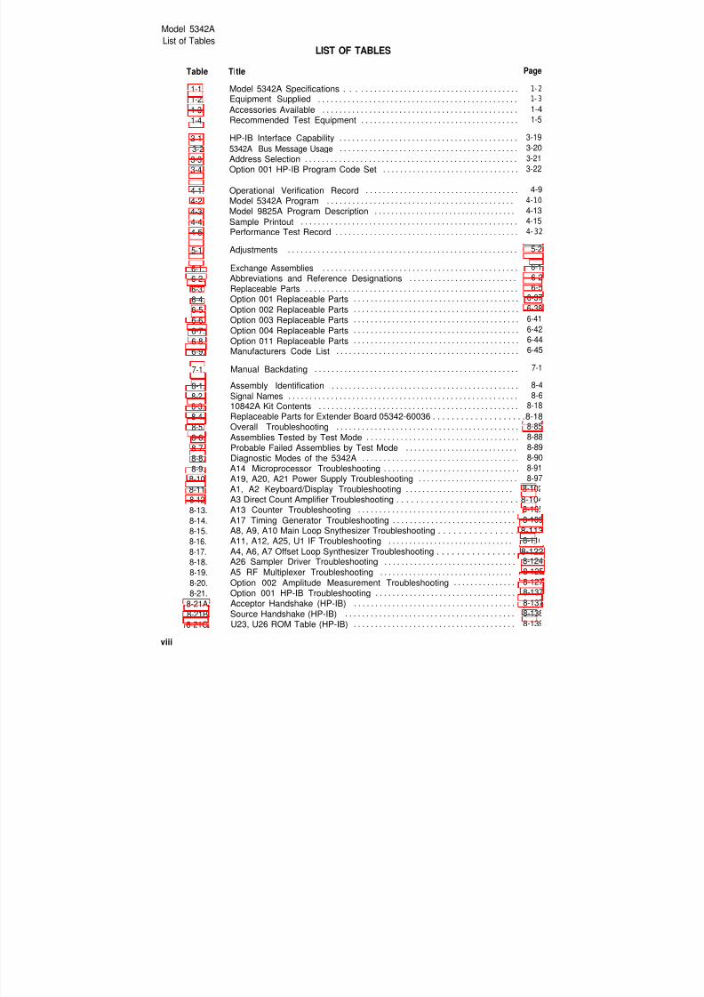
List of TablesLIST OF TABLES
Table Title Page
1-1. Model 5342A Specifications . . . . . . . . . . . . . . . . . . . . . . . . . . . . . . . . . . . . . . . . 1- 2
1-2. Equipment Supplied . . . . . . . . . . . . . . . . . . . . . . . . . . . . . . . . . . . . . . . . . . . . . . . 1- 3
1-3. Accessories Available . . . . . . . . . . . . . . . . . . . . . . . . . . . . . . . . . . . . . . . . . . . . . . 1-4
1-4. Recommended Test Equipment . . . . . . . . . . . . . . . . . . . . . . . . . . . . . . . . . . . . . 1-5
3-1. HP-IB Interface Capability 3-19. . . . . . . . . . . . . . . . . . . . . . . . . . . . . . . . . . . . . . . . . .3-2 5342A Bus Message Usage . . . . . . . . . . . . . . . . . . . . . . . . . . . . . . . . . . . . . . . . . . 3-20
3-3. Address Selection . . . . . . . . . . . . . . . . . . . . . . . . . . . . . . . . . . . . . . . . . . . . . . . . . . 3-21
3-4. Option 001 HP-IB Program Code Set . . . . . . . . . . . . . . . . . . . . . . . . . . . . . . . . 3-22
4-1. Operational Verification Record . . . . . . . . . . . . . . . . . . . . . . . . . . . . . . . . . . . . 4-9
4-2. Model 5342A Program . . . . . . . . . . . . . . . . . . . . . . . . . . . . . . . . . . . . . . . . . . . . 4-10
4-3. Model 9825A Program Description . . . . . . . . . . . . . . . . . . . . . . . . . . . . . . . . . . 4-13
4-4. Sample Printout . . . . . . . . . . . . . . . . . . . . . . . . . . . . . . . . . . . . . . . . . . . . . . . . . . . 4-15
4-5. Performance Test Record . . . . . . . . . . . . . . . . . . . . . . . . . . . . . . . . . . . . . . . . . . . 4- 32
5-1. Adjustments . . . . . . . . . . . . . . . . . . . . . . . . . . . . . . . . . . . . . . . . . . . . . . . . . . . . . . 5-2
6-1.6-2.6-3.6-4.6-5.
6-6.
6-7.6-8.6-9.
Exchange Assemblies . . . . . . . . . . . . . . . . . . . . . . . . . . . . . . . . . . . . . . . . . . . . . . 6-1Abbreviations and Reference Designations . . . . . . . . . . . . . . . . . . . . . . . . . . 6-2
Replaceable Parts . . . . . . . . . . . . . . . . . . . . . . . . . . . . . . . . . . . . . . . . . . . . . . . . . . 6-5
Option 001 Replaceable Parts . . . . . . . . . . . . . . . . . . . . . . . . . . . . . . . . . . . . . . . 6-37
Option 002 Replaceable Parts . . . . . . . . . . . . . . . . . . . . . . . . . . . . . . . . . . . . . . . 6-38
Option 003 Replaceable Parts . . . . . . . . . . . . . . . . . . . . . . . . . . . . . . . . . . . . . . . 6-41
Option 004 Replaceable Parts . . . . . . . . . . . . . . . . . . . . . . . . . . . . . . . . . . . . . . . 6-42
Option 011 Replaceable Parts . . . . . . . . . . . . . . . . . . . . . . . . . . . . . . . . . . . . . . . 6-44
Manufacturers Code List . . . . . . . . . . . . . . . . . . . . . . . . . . . . . . . . . . . . . . . . . . . 6-45
7-1. Manual Backdating . . . . . . . . . . . . . . . . . . . . . . . . . . . . . . . . . . . . . . . . . . . . . . . . 7-1
8-1.8-2.
8-3.8-4.8-5.8-6.
8-7.8-8.
8-9.8-10.
8-11.8-12.8-13.8-14.8-15.
8-16.8-17.8-18.8-19.
8-20.8-21.
8-21A.8-21B.8-21C.
Assembly Identification . . . . . . . . . . . . . . . . . . . . . . . . . . . . . . . . . . . . . . . . . . . . 8-4
Signal Names . . . . . . . . . . . . . . . . . . . . . . . . . . . . . . . . . . . . . . . . . . . . . . . . . . . . . . 8-6
10842A Kit Contents . . . . . . . . . . . . . . . . . . . . . . . . . . . . . . . . . . . . . . . . . . . . . . . 8-18Replaceable Parts for Extender Board 05342-60036 . . . . . . . . . . . . . . . . . . . . 8-18Overall Troubleshooting . . . . . . . . . . . . . . . . . . . . . . . . . . . . . . . . . . . . . . . . . . . 8-85
Assemblies Tested by Test Mode . . . . . . . . . . . . . . . . . . . . . . . . . . . . . . . . . . . . 8-88
Probable Failed Assemblies by Test Mode . . . . . . . . . . . . . . . . . . . . . . . . . . . 8-89
Diagnostic Modes of the 5342A . . . . . . . . . . . . . . . . . . . . . . . . . . . . . . . . . . . . . 8-90
A14 Microprocessor Troubleshooting . . . . . . . . . . . . . . . . . . . . . . . . . . . . . . . . 8-91
A19, A20, A21 Power Supply Troubleshooting . . . . . . . . . . . . . . . . . . . . . . . . 8-97
A1, A2 Keyboard/Display Troubleshooting . . . . . . . . . . . . . . . . . . . . . . . . . . 8-102
A3 Direct Count Amplifier Troubleshooting . . . . . . . . . . . . . . . . . . . . . . . . . 8-104A13 Counter Troubleshooting . . . . . . . . . . . . . . . . . . . . . . . . . . . . . . . . . . . . . 8-105
A17 Timing Generator Troubleshooting . . . . . . . . . . . . . . . . . . . . . . . . . . . . . 8-109
A8, A9, A10 Main Loop Snythesizer Troubleshooting . . . . . . . . . . . . . . . . 8-113
A11, A12, A25, U1 IF Troubleshooting . . . . . . . . . . . . . . . . . . . . . . . . . . . . . . 8-116A4, A6, A7 Offset Loop Synthesizer Troubleshooting . . . . . . . . . . . . . . . . . 8-122A26 Sampler Driver Troubleshooting . . . . . . . . . . . . . . . . . . . . . . . . . . . . . . . 8-124
A5 RF Multiplexer Troubleshooting 8-125. . . . . . . . . . . . . . . . . . . . . . . . . . . . . . . .
Option 002 Amplitude Measurement Troubleshooting . . . . . . . . . . . . . . . 8-127
Option 001 HP-IB Troubleshooting . . . . . . . . . . . . . . . . . . . . . . . . . . . . . . . . . 8-137
Acceptor Handshake (HP-IB) . . . . . . . . . . . . . . . . . . . . . . . . . . . . . . . . . . . . . . 8-137
Source Handshake (HP-IB) . . . . . . . . . . . . . . . . . . . . . . . . . . . . . . . . . . . . . . . . 8-138
U23, U26 ROM Table (HP-IB) . . . . . . . . . . . . . . . . . . . . . . . . . . . . . . . . . . . . . . 8-139
viii
8/21/2019 HP5432 Microwave Frequency Counter
http://slidepdf.com/reader/full/hp5432-microwave-frequency-counter 11/364
Model 5342A
List of Figures
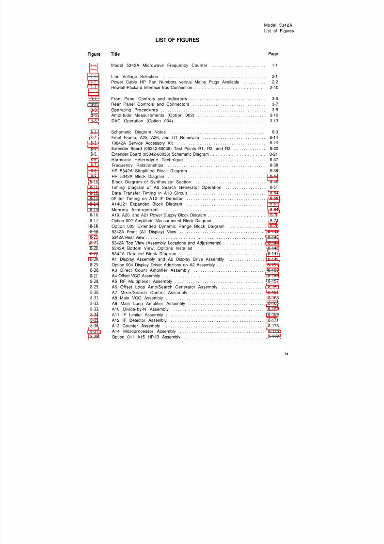
LIST OF FIGURES
Figure
1-1.
2- 1.
2- 2.
2- 3.
3-1.
3-2.
3-3.
3-4.
3-5.
8- 1.
8- 2.
8- 3.
8- 4.
8- 5.
8- 6.
8- 7.
8- 8.
8- 9.
8-10.
8-11.
8-12.
8-13.
8-14.
8-15.
8-16.
8-17.8-18.
8-19.
8- 20.
8-21.
8-22.
8-23.8-24.
8-25.
8-26.
8- 27.
8-28.
8-29.8-30.
8-31.
8-32.
8-33.
8-34.
8-35.
8-36.
8-37.
8-38.
Title Page
Model 5342A Microwave Frequency Counter . . . . . . . . . . . . . . . . . . . . . . . . 1-1
Line Voltage Selection . . . . . . . . . . . . . . . . . . . . . . . . . . . . . . . . . . . . . . . . . . . . . 2-1
Power Cable HP Part Numbers versus Mains Plugs Available . . . . . . . . . . 2-2
Hewlett-Packard Interface Bus Connection . . . . . . . . . . . . . . . . . . . . . . . . . 2-10
Front Panel Controls and Indicators . . . . . . . . . . . . . . . . . . . . . . . . . . . . . . . . . 3-5
Rear Panel Controls and Connectors . . . . . . . . . . . . . . . . . . . . . . . . . . . . . . . . 3-7
Operat ing Procedures . . . . . . . . . . . . . . . . . . . . . . . . . . . . . . . . . . . . . . . . . . . . . . 3-8
Ampli tude Measurements (Option 002) . . . . . . . . . . . . . . . . . . . . . . . . . . . . . . 3-12
DAC Operation (Option 004) . . . . . . . . . . . . . . . . . . . . . . . . . . . . . . . . . . . . . . . 3-13
Schematic Diagram Notes . . . . . . . . . . . . . . . . . . . . . . . . . . . . . . . . . . . . . . . . . 8-3
Front Frame, A25, A26, and U1 Removale . . . . . . . . . . . . . . . . . . . . . . . . . . . . 8-14
10842A Service Accessory Kit . . . . . . . . . . . . . . . . . . . . . . . . . . . . . . . . . . . . . . . 8-19
Extender Board (05342-60036) Test Points R1, R2, and R3 . . . . . . . . . . . . . . 8-20Extender Board (05342-60036) Schematic Diagram . . . . . . . . . . . . . . . . . . . . . 8-21
Harmonic Heterodyne Techn ique . . . . . . . . . . . . . . . . . . . . . . . . . . . . . . . . . . . 8-37
Frequency Relationships . . . . . . . . . . . . . . . . . . . . . . . . . . . . . . . . . . . . . . . . . . . 8-38
HP 5342A Simplified Block Diagram . . . . . . . . . . . . . . . . . . . . . . . . . . . . . . . . . 8-39
HP 5342A Block Diagram . . . . . . . . . . . . . . . . . . . . . . . . . . . . . . . . . . . . . . . . . . . 8-44
Block Diagram of Synthesizer Section . . . . . . . . . . . . . . . . . . . . . . . . . . . . . . . 8-45
Timing Diagram of A6 Search Generator Operation . . . . . . . . . . . . . . . . . . 8-51
Data Transfer Timing in A10 Circuit . . . . . . . . . . . . . . . . . . . . . . . . . . . . . . . . . 8-54
0Filter Timing on A12 IF Detector . . . . . . . . . . . . . . . . . . . . . . . . . . . . . . . . . . . 8-58
A14U21 Expanded Block Diagram . . . . . . . . . . . . . . . . . . . . . . . . . . . . . . . . . . . 8-61
Memory Ar ran gem ent . . . . . . . . . . . . . . . . . . . . . . . . . . . . . . . . . . . . . . . . . . . . . 8-64
A19, A20, and A21 Power Supply Block Diagram . . . . . . . . . . . . . . . . . . . . . . 8-70
Option 002 Amplitude Measurement Block Diagram . . . . . . . . . . . . . . . . . . 8-74Option 003 Extended Dynamic Range Block Daigram . . . . . . . . . . . . . . . . . 8-78
5342A Front (A1 Display) View . . . . . . . . . . . . . . . . . . . . . . . . . . . . . . . . . . . . . 8-142
5342A Rear View . . . . . . . . . . . . . . . . . . . . . . . . . . . . . . . . . . . . . . . . . . . . . . . . . 8-143
5342A Top View (Assembly Locations and Adjustments) . . . . . . . . . . . . . . 8-144
5342A Bottom View, Options Installed . . . . . . . . . . . . . . . . . . . . . . . . . . . . . . 8-145
5342A Detailed Block Diagram . . . . . . . . . . . . . . . . . . . . . . . . . . . . . . . . . . . . . 8-147
A1 Display Assembly and A2 Display Drive Assembly . . . . . . . . . . . . . . . . 8-149
Option 004 Display Driver Additions on A2 Assembly . . . . . . . . . . . . . . . . 8-151
A3 Direct Count Amplifier Assembly . . . . . . . . . . . . . . . . . . . . . . . . . . . . . . . 8-153
A4 Offset VCO Assembly . . . . . . . . . . . . . . . . . . . . . . . . . . . . . . . . . . . . . . . . . . 8-155
A5 RF Multiplexer Assembly . . . . . . . . . . . . . . . . . . . . . . . . . . . . . . . . . . . . . . . 8-157
A6 Offset Loop Amp/Search Generator Assembly . . . . . . . . . . . . . . . . . . . 8-159
A7 Mixer/Search Control Assembly . . . . . . . . . . . . . . . . . . . . . . . . . . . . . . . . 8-161
A8 Main VCO Assembly . . . . . . . . . . . . . . . . . . . . . . . . . . . . . . . . . . . . . . . . . . . 8-163
A9 Main Loop Amplifier Assembly . . . . . . . . . . . . . . . . . . . . . . . . . . . . . . . . . 8-165
A10 Divide-by-N Assembly . . . . . . . . . . . . . . . . . . . . . . . . . . . . . . . . . . . . . . . . 8-167
A11 IF Limiter Assembly . . . . . . . . . . . . . . . . . . . . . . . . . . . . . . . . . . . . . . . . . . . 8-169
A12 IF Detector Assembly . . . . . . . . . . . . . . . . . . . . . . . . . . . . . . . . . . . . . . . . . 8-171
A13 Counter Assembly . . . . . . . . . . . . . . . . . . . . . . . . . . . . . . . . . . . . . . . . . . . . 8-173
A14 Microprocessor Assembly . . . . . . . . . . . . . . . . . . . . . . . . . . . . . . . . . . . . . 8-175
Option 011 A15 HP-IB Assembly . . . . . . . . . . . . . . . . . . . . . . . . . . . . . . . . . . . 8-177
ix

8/21/2019 HP5432 Microwave Frequency Counter
http://slidepdf.com/reader/full/hp5432-microwave-frequency-counter 12/364
Model 5342AList of Figures
Figure
8-39.
8-40.8-41.8-42.8-43.8-44.8-45.8-46.
LIST OF FIGURES (Continued)
Title
Option 002 A16 Amplitude Measurements,A27 Low Frequency Amplifier, and
U2 High Frequency Amplifier Assemblies . . . . . . . . . . ....Option 003 A16 Extended Dynamic Range Assembly . . . . . . . . . . . . . . . . .A17 Timing Generator Assembly . . . . . . . . . . . . . . . . . . . . . . . . . . . . . . . . . . .A18 Time Base Buffer Assembly . . . . . . . . . . . . . . . . . . . . . . . . . . . . . . . . . . . .A19, A20, A21, and A23 Power Supply Assembly . . . . . . . . . . . . . . . . . . . . .A24 Oscillator Assemblies . . . . . . . . . . . .’ . . . . . . . . . . . . . . . . . . . . . . . . . . . . .A25 Preamplifier Assembly . . . . . . . . . . . . . . . . . . . . . . . . . . . . . . . . . . . . . . . .A26 Sampler Driver Assembly . . . . . . . . . . . . . . . . . . . . . . . . . . . . . . . . . . . . . .
Page
8-1798-1818-1838-1858-1878-1898-1918-193
x

8/21/2019 HP5432 Microwave Frequency Counter
http://slidepdf.com/reader/full/hp5432-microwave-frequency-counter 13/364
TM 11-6625-3014-14
0-1. SCOPE.
SECTION O
INSTRUCTIONS
This manual describes Microwave Frequency Counter TD-1225A(V)l/U (fig. l-l)
and provides maintenance instructions. Throughout this manual, the TD-1225A(V)l/U
is refered to as the Hewlett-Packard (HP) Model 5342A.
0-2. INDEXES OF PUBLICATIONS.
a. DA Pam 310-4.
whether there are new
to the equipment.
b. DA Pam 310-7.
Refer to the latest issue of DA Pam 310-4 to determineeditions, changes, or additional publications pertaining
Refer to DA Pam 310-7 to determine whether there are
modification work orders (MWO’S) pertaining to the equipment.
0-3. FORMS AND RECORDS.
a. Reports of Maintenance and Unsatisfactory Equipment. Maintenance
forms, records, and reports which are used by maintenance personnel at alllevels of maintenance are listed in and prescribed by TM 38-750.
b. Report of Packaging and Handling Deficiencies. Fill out and forward
SF 364 (Report of Discrepancy (ROD))as prescribed in AR 735-11-2/DLAR
4140.55/NAVSUPINST 4610.33B/AFR 75-18/MCO p4610.19C and DLAR 4500.15.
c. Discrepancy in Shipment Report (DISREP) (SF 361). Fill out andforward Discrepancy in Shipment Report (DISREP) (SF 361) as prescribed in
AR 55-38/NAVSUPINST 4610.33B/AFR 75-18/MCO P4610.19C and DLAR 4500.15.
0-4. REPORTING OF EQUIPMENT IMPROVEMENT RECOMMENDATIONS (EIR).
EIR’s will be prepared using DA Form 2407, Maintenance Request.Instructions for preparing EIR’s are provided in TM 38-750, The ArmyMaintenance Management System. EIR’s should be mailed directly to
Commander, US Army Communications and Electronics Materiel Readiness Command,ATTN: DRSEL-ME-MQ, Fort Monmouth, New Jersey 07703. A reply will be
furnished directly to you.
0-5. ADMINISTRATIVE STORAGE.
Administrative storage of equipment issued to and used by Army activities
shall be in accordance with TM 740-90-1.
0-6. DESTRUCTION OF ARMY ELECTRONICS MATERIEL.
Destruction of Army electronics materiel to prevent enemy use shall be inaccordance with TM 750-244-2.
0-1

8/21/2019 HP5432 Microwave Frequency Counter
http://slidepdf.com/reader/full/hp5432-microwave-frequency-counter 14/364
Model 5342AGeneral Information
SECTION IGENERAL INFORMATION
1-1. INTRODUCTION
1-1. This manual provides operating and service information for the Hewlett-Packard Model5342A Microwave Frequency Counter, shown in Figure 1-1.
1-3. SPECIFICATIONS
1-4. Specifications of the 5342A are listed in Ta b le 1-1.
Figure 1-1. Model 5342A Microwave Frequency Counter
1-1

8/21/2019 HP5432 Microwave Frequency Counter
http://slidepdf.com/reader/full/hp5432-microwave-frequency-counter 15/364
Model 5342AGeneral Information
1-2
Ta b l e 1 - 1. Mo d e l 5342 A S p e c i f i c a t i o n s
INPUT CHARACTERISTICS
INPUT 1:
Frequency range: 500 MHz t o 18 GHz
Sensitivity:
500 MHz t o 12. 4 GHz - 25 dBm
12. 4 GHz t o 18 GHz - 20 dBm
Maximum input: +5 dBm ( see Opt i ons 002, 003f or hi gher l evel ).
Dynamic range:
500 MHz t o 12. 4 GHz 30 dB12. 4 GHz t o 18 GHz 25 dB
Impedance: 50 ohms, nomi nal
Connector: Preci si on Type N f emal eDamage level: +25 dBm, peak
Coupling: dc t o l oad, ac to i nstr ument .
SWR:<2: 1, 500 MHz—10 GHz
<3: 1, 10 GHz—18 GHzFM tolerance: Swi t ch sel ect abl e (r ear panel )
FM (wide): 50 MHz p- p wor st case.CW ( nor mal ) : 20 MHz p- p wors t case.
For modul at i on r ates f r om dc to 10 MHz.
AM tolerance: Any modul at i on i ndex provi dedt he mi nimum si gnal l evel i s not l ess than the
sensi t i v it y speci f i cat i on.
Automatic amplitude discrimination: Aut omat i -
cal l y measures t he l argest of al l si gnal s pres-
ent , provi di ng t hat si gnal i s 6 dB above anysi gnal wi t hi n 500 MHz; 20dB above any si gnal ,
500 MHz—18 GHz.Modes of operation:
Automatic: Counter aut omati cal l y acqui r esand di spl ays hi ghest l evel si gnal wi t hi n sensi -
ti vi ty range.Manual: Cent er f r equency enter ed t o wi t hi n
±50 MHz t o t r ue val ue.
Acquisition time:
Automatic mode: Nor mal FM 530 ms worst
case; wi de FM 2.4 s worst case.Manual mode: 80 ms af t er f r equency ent ered.
INPUT 2:Frequency range: 10 Hz t o 520 MHz Di r ect
Count.
Sensitivity:50 10 Hz t o 520 MHz 25 mV r ms,
1 M 10 Hz t o 25 MHz 50 mV r ms.
Impedance: Sel ect abl e: 1 MW, <50 pF or 50Wnomi nal .
Coupling: acConnector: Type BNC f emal e.
Maximum input: Ω 3. 5V rms ( +24 dBm) or 5Vdc f use prot ect ed; 1 MW 200V dc +5. 0V r ms.
TIME BASE
Crystal frequency: 10 MHz
Stability:Aging rate: <1 X 10- 7 per mont h.
Short term:
50°C.L i n e v a r i a t i o n :
nomi nal .
( TTL compat i bl e); 1. 5V peak- t o-peak i nto
W avai l abl e f rom rear panel BNC.
External time base: Requi r es 10 MHz, 2. 0V peak-
t o- peak si ne wave or squar e wave i nto 1 KW
vi a r ear panel BNC connect or. Swi t ch
sel ects ei t her i nternal or ext ernal ti me base.
OPTIONAL TIME BASE
(OPTION 001)
Opti on 001 pr ovi des an oven-cont r ol l ed cr yst al
osci l l ator t i me base, 10544A ( see separ ate dat asheet) , t hat r esul t s i n bet t er accuracy and l onger
per i ods bet ween cal i brati on.
Crystal frequency: 10 MHz
Stability:
Aging rate:
up.T e m p e r a t u r e :
50°C.Short term:L i ne va r i a t i o n :
nomi nal .Warm-up:
aft er t urn- on, at 25°C.
AMPLITUDE MEASUREMENT
(OPTION 002)Opti on 002 provi des t he capabi l i t y of measuri ngt he ampl i t ude of t he i ncomi ng si ne wave si gnal ,
and si mul t aneousl y di spl ayi ng i t s f requency ( MHz)and l evel ( dBm) . The maxi mum operat i ng l evel
and t he t op end of dynami c r ange are i ncreased t o+20 dBm. Ampl i t ude off set t o 0. 1 dB resol uti on
may be sel ected fr om f r ont panel pushbutt ons.
INPUT 1:Frequency range: 500 MHz—18 GHz,
Dynamic range (frequency and level):- 22 dBm t o +20 dBm 500 MHz t o 12. 4 GHz
- 15 dBm t o +20 dBm 12. 4 GHz t o 18 GHzMaximum operating level: +20 dBm
Damage level: +25 dBm, peakResolution: 0. 1 dB
Accuracy: ±1. 5 dB ( excl udi ng mi smat chuncertai nty).
SWR:<2: 1 ( ampl i t ude measurement) .<5: 1 ( f r equency measurement) .
Measurement time: 100 ms + f r equency mea-
sur ement t i me.
Display: Si mul t aneousl y di spl ays f r equency t o 1MHz r esol uti on and i nput l evel . ( Opti on 011provi des ful l f requency resol ut i on on HP-I Boutput . )
INPUT 2: ( 500 i mpedance onl y)Frequency range: 10 MHz—520 MHz
Dynamic range (frequency and level):
- 17 dBm t o +20 dBm.Damage level: +24 dBm, peak
Resolution: 0. 1 dBm.
Accuracy: 1. 5 dB (excl udi ng mi smatch
uncertai nty).
SWR: <1. 8: 1Measurement time: 100 ms + f r equency mea-
sur ement t i me.
Display: Si mul t aneousl y di spl ays f r equency to 1
MHz r esol uti on and i nput l evel .

8/21/2019 HP5432 Microwave Frequency Counter
http://slidepdf.com/reader/full/hp5432-microwave-frequency-counter 16/364
Model 5342A
General Information
Table 1-1. Mod el 5342A Spe c ific at ions (Co ntinued )
EXTENDED DYNAMIC RANGE GENERAL
(OPTION 003) Accuracy: ±1 count ± time base error.Option 003 provides an attenuator that automati- Resolution: Front panel pushbuttons select 1 Hz to
cally extends the dynamic range of operation for 1 MHz.input 1. Residual stability: When counter and source use
INPUT 1:common time base or counter uses external
Frequency range: 500 MHz to 18 GHz higher stability time base, <4 X 10-11
r m sSensitivity:
typcial.
500 MHz to 12.4 GHz -22 dBDisplay: 11-digit LED display, sectionalized to
12.4 GHz to 18 GHz -15 dBmread GHz, MHz, kHz, and Hz.
Maximum operating level: +20 dBm.Self-check: Selected from front panel push-
Dynamic range:buttons. Measures 75 MHz for resolution
500 MHz to 12.4 GHz 42 dBchosen.
12.4 GHz to 18 GHz 35 dBFrequency offset: Selected from front panel
Damage level: +25 dBm, peakpushbuttons. Displayed frequency is offset by
SWR: <5:1entered value to 1 Hz resolution.
Sample rate: Variable from less than 20 ms be-tween measurements to HOLD which holds
DIGITAL-TO-ANALOG CONVERTER display indefinitely.(OPTION 004) IF out: Rear panel BNC connector provides 25
Option 004 provides the ability to convert any MHz to 125 MHz output of down-convertedthree consecutive displayed digits into an analog microwave signal.
voltage output. A display of ∅∅∅ produces ∅ V out- Operating temperature: 0°C to 50°C.put; 999 produces 9.99V full scale. Power requirements: 100/120/220/240V rms, +5%,Accuracy: ±5 mV, ±0.3 mV/°C (from 25°C) -10%, 48—66 Hz; 100 VA max.Conversion Speed: Accessories furnished: Power cord, 229 cm (7½ ft.)
reading. Size: 133 mm H X 213 mm WX 498 mm DResolution: 10 mV
Output: 5 mA. Impedance <1.0 ohm. Weight: Net 9.1 kg (20 Ibs.).Connector: Type BNC female on rear panel. Shipping 12.7 kg (28 Ibs.).
1-5. SAFETY CONSIDERATIONS
1-6. This product is a Safety Class I instrument (provided with a protective earth terminal). Safetyinformation pertinent to the operation and servicing of this instrument is included in appropriate
sections of this manual.
1 - 7 . I N S T R U M E N T I D E N T I F I C A T I O N
1-8. Hewlett-Packard instruments have a 2-section, 10-character serial number (0000A00000),
which is located on the rear panel. The four-digit serial prefix identifies instrument changes. If
the serial prefix of your instrument differs from that listed on the title page of this manual, there
are differences between this manual and your instrument. Instruments having higher serial
prefixes are covered with a “Manual Changes” sheet included with this manual. If the change
sheet is missing, contact the nearest Hewlett-Packard Sales and Service Office listed at the back of
this manual. Instruments having a lower serial prefix than that listed on the title page, are covered
in Section VII.
1-9. ACCESSORIES
1-10. Table 1-2 lists accessory equipment supplied and Table 1-3 lists accessories available.
Tab le 1-2. Equipm ent Supp lied
DESCRIPTION HP PART NUMBER
Detachable Power Cord 229 cm (7½ feet long) 8120-1378
1-3

8/21/2019 HP5432 Microwave Frequency Counter
http://slidepdf.com/reader/full/hp5432-microwave-frequency-counter 17/364
Model 5342A
General Information
Tab le 1-3. Acc essor ies Avai lab le
DESCRIPTION HP PART NUMBER
Bail Handle Kit 5061-2002
Rack Mounting Adapter Kit (Option 908) 5061-0057
Rack Mounting Adapter Kit with slot for access K70-59992A
to front connectors from rear.
Transit Case 9211-2682
Service Accessory Kit (refer to paragraph 1-16) Model 10842A
Microwave Attenuators Model 8491B, 8494/5/6H
Signature Analyzer Model 5004A
1-11. DESCRIPTION
1-12. The 5342A Microwave Frequency Counter measures the frequency of signals in the rangeof 10 Hz to 18 GHz, with a basic sensitivity of -25 dBm. Signals in the frequency range of 10 Hz to500 MHz are measured by the direct count method. Signals in the frequency range of 500 MHz to18 GHz are down-converted to an IF by a heterodyne conversion technique for application to the
counter circuits. The unique conversion technique employed results in high sensitivity and FMtolerance in addition to automatic amplitude discrimination. The counted IF is added to the localoscillator frequency to determine the unknown frequency for display.
1-13. OPTIONS
1-14. Options available with the 5342A are described in Table 1-1 and paragraph 3-57. If anoption is included in the initial order, it will be installed at the factory and ready for operationupon receipt. If an option is ordered for field installation it will be supplied as a retrofit kit. Referto Section II for kit part numbers and installation instructions.
1-15. SERVICE EQUIPMENT AVAILABLE
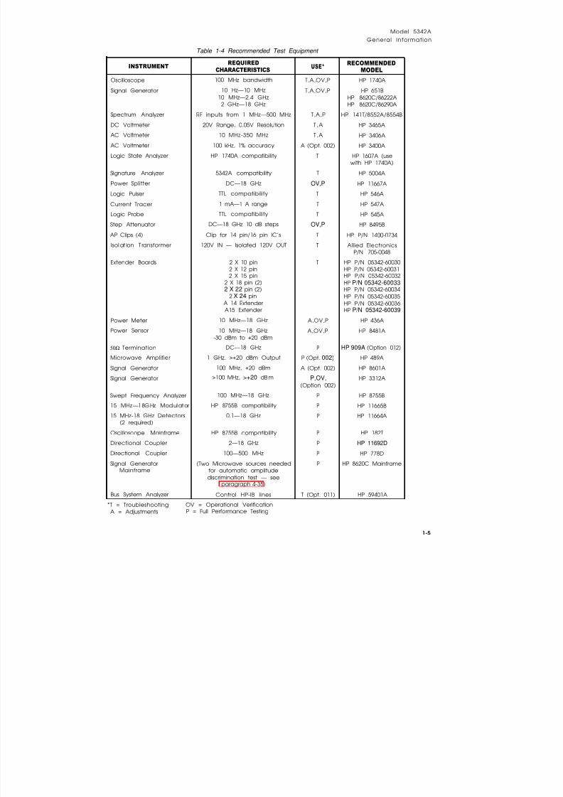
1-16. Extender boards are available for servicing printed circuit assemblies while extended fromthe instrument. The extender boards allow assemblies to be extended from their plug-in con-nectors for monitoring with appropriate test equipment. Extender boards for each assembly aresupplied in Service Accessory Kit 10842A as described in paragraph 8-46.
1-17. RECOMMENDED TEST EQUIPMENT
1-18. The test equipment listed in Table 1-4 is recommended for use during performance tests,adjustments, and troubleshooting. Substitute test equipment may be used if it meets the requiredcharacteristics listed in the table.
1-4
8/21/2019 HP5432 Microwave Frequency Counter
http://slidepdf.com/reader/full/hp5432-microwave-frequency-counter 18/364
Model 5342A
General Information
Table 1-4 Recommended Test Equipment
INSTRUMENTREQUIRED
USE*RECOMMENDED
CHARACTERISTICS MODEL
Oscilloscope 100 MHz bandwidth T,A,OV,P HP 1740A
Signal Generator 10 Hz—10 MHz T,A,OV,P HP 651B10 MHz—2.4 GHz HP 8620C/86222A
2 GHz—18 GHz HP 8620C/86290A
Spectrum Analyzer RF inputs from 1 MHz—500 MHz T,A,P HP 141T/8552A/8554B
DC Voltmeter 20V Range, 0.05V Resolution T ,A HP 3465A
AC Voltmeter 10 MHz-350 MHz T ,A HP 3406A
AC Voltmeter 100 kHz, 1% accuracy A (Opt. 002) HP 3400A
Logic State Analyzer HP 1740A compatibility T HP 1607A (usewith HP 1740A)
Signature Analyzer 5342A compatibility T HP 5004A
Power Splitter DC—18 GHz OV,P HP 11667A
Logic Pulser TTL compatibility T HP 546A
Current Tracer 1 mA—1 A range T HP 547A
Logic Probe TTL compatibility T HP 545AStep Attenuator DC—18 GHz 10 dB steps OV,P HP 8495B
AP Clips (4) Clip for 14 pin/16 pin IC’s T HP P/N 1400-0734
Isolat ion T ransformer 120V IN — Isolated 120V OUT T Allied ElectronicsP/N 705-0048
Extender Boards 2 X 10 pin T HP P/N 05342-600302 X 12 pin HP P/N 05342-600312 X 15 pin HP P/N 05342-60032
2 X 18 pin (2) HP P/N 05342-600332 X 22 pin (2) HP P/N 05342-60034
2 X 24 pin HP P/N 05342-60035A 14 Extender HP P/N 05342-60036A15 Extender HP P/N 05342-60039
Power Meter 10 MHz—18 GHz A,OV,P HP 436A
Power Sensor 10 MHz—18 GHz A,OV,P HP 8481A-30 dBm to +20 dBm
50Ω Termination DC—18 GHz P HP 909A (Option 012)
Microwave Amplifier 1 GHz, >+20 dBm Output P (Opt. 002) HP 489A
Signal Generator 100 MHz, +20 dBm A (Opt. 002) HP 8601A
Signal Generator >100 MHz, >+20 dB m P,OV, HP 3312A(Option 002)
Swept Frequency Analyzer 100 MHz—18 GHz P HP 8755B
15 MHz—18GHz Modulator HP 8755B compatibility P HP 11665B
15 MHz-18 GHz Detectors 0.1—18 GHz P HP 11664A(2 required)
Oscilloscope Mainframe HP 8755B compatibility P HP 182TDirectional Coupler 2—18 GHz P HP 11692D
Directional Coupler 100—500 MHz P HP 778D
Signal Generator (Two Microwave sources needed P HP 8620C MainframeMainframe for automatic amplitude
discrimination test — seeparagraph 4-35)
Bus System Analyzer Control HP-IB lines T (Opt. 011) HP 59401A
*T = Troubleshooting OV = Operational VerificationA = Adjustments P = Full Performance Testing
1-5

8/21/2019 HP5432 Microwave Frequency Counter
http://slidepdf.com/reader/full/hp5432-microwave-frequency-counter 19/364
Model 5342A
Installation
SECTION IIINSTALLATION
2-1. INTRODUCTION
2-2. This section contains information for unpacking, inspection, storage, and installation.
2-3. UNPACKING AND INSPECTION
2-4. If the shipping carton is damaged, inspect the instrument for visible damage (scratches,
dents, etc.). If the instrument is damaged, notify the carrier and the nearest Hewlett-Packard
Sales and Service Office immediately (offices are listed at the back of this manual). Keep the
shipping carton and packing material for the carrier’s inspection. The Hewlett-Packard Sales
and Service Office will arrange for repair or replacement of your instrument without waiting for
the claim against the carrier to be settled.
2-5. INSTALLATION REQUIREMENTS
CAUTION
Before connecting the instrument to ac power lines,
be sure that the voltage selector is properly
positioned as described below.
2-6. LINE VOLTAGE REQUIREMENTS. The 5342A is equipped with a power module that con-
tains a printed-circuit line voltage selector to select 100- 120-, 220-, or 240-volt ac operation.
Before applying power, the pc selector must be set to the correct position and the correct fuse
must be installed as described below.
2-7. Power line connections are selected by the position of the plug-in circuit card in the
module. When the card is plugged into the module, the only visible markings on the card indi-
cate the line voltage to be used. The correct value of line fuse, with a 250-voIt rating, must beinstalled after the card is inserted. This instrument uses a 0.75A fuse (HP Part No. 2110-0360) for
100/120-volt operation; a 0.375A fuse (HP Part No. 2110-0421) for 220/240-volt operation.
2-8. To convert from one line voltage to another, the power cord must be disconnected from
the power module before the sliding window covering the fuse and card compartment can be
moved to expose the fuse and circuit card. See Figure 2-1.
Figure 2-1. Line Voltage Selection
2-1
8/21/2019 HP5432 Microwave Frequency Counter
http://slidepdf.com/reader/full/hp5432-microwave-frequency-counter 20/364
Model 5342A
Installation
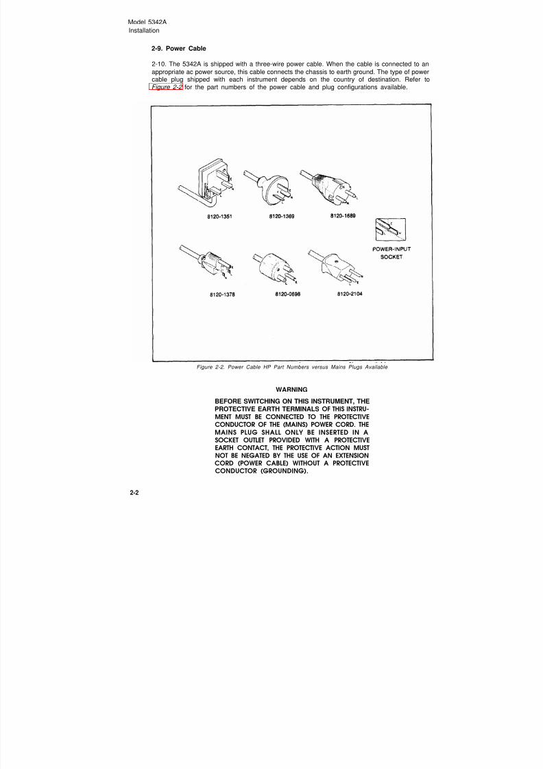
2-9. Power Cable
2-10. The 5342A is shipped with a three-wire power cable. When the cable is connected to an
appropriate ac power source, this cable connects the chassis to earth ground. The type of powercable plug shipped with each instrument depends on the country of destination. Refer toFigure 2-2 for the part numbers of the power cable and plug configurations available.
Figure 2-2. Power Cable HP Part Numbers versus Mains Plugs Available
WARNING
BEFORE SWITCHING ON THIS INSTRUMENT, THEPROTECTIVE EARTH TERMINALS OF THIS INSTRU-
MENT MUST BE CONNECTED TO THE PROTECTIVECONDUCTOR OF THE (MAINS) POWER CORD. THEMAINS PLUG SHALL ONLY BE INSERTED IN ASOCKET OUTLET PROVIDED WITH A PROTECTIVEEARTH CONTACT, THE PROTECTIVE ACTION MUSTNOT BE NEGATED BY THE USE OF AN EXTENSIONCORD (POWER CABLE) WITHOUT A PROTECTIVECONDUCTOR (GROUNDING).
2-2
8/21/2019 HP5432 Microwave Frequency Counter
http://slidepdf.com/reader/full/hp5432-microwave-frequency-counter 21/364
Model 5342A
Installation
2-11. Operating Environment
2-12. TEMPERATURE. The 5342A may be operated in temperatures from 0°C to +55°C.
2-13. HUMIDITY. The 5342A may be operated in environments with humidity up to 95%. How-
ever, it should be protected from temperature extremes which cause condensation in the
instrument.
2-14. ALTITUDE. The 5342A may be operated at altitudes up to 4,600 metres (15,000 feet).
2 - 1 5 . S T O R A G E A N D S H I P M E N T
2-16. Environment
2-17. The instrument may be stored or shipped in environments within the following limits:
TEMPERATURE . . . . . . . . . . . . . . . . . -40°C to +75°C
HUMIDITY . . . . . . . . . . . . . . . . . . . . . . . . . . Up to 95%
ALTITUDE . . . . . . . . . . . . . 7,620 metres (25,000 feet)
2-18. The instrument should also be protected from temperature extremes which causecondensation within the instrument.
2-19. Packaging
2-20. ORIGINAL PACKAGING. Containers and materials identical to those used in factory
packaging are available through Hewlett-Packard offices. If the instrument is being returned to
Hewlett-Packard for servicing, attach a tag indicating the type of service required, return address,
model number, and full serial number. Also, mark the container FRAGILE to ensure careful
handling. In any correspondence, refer to the instrument by model number and full serial
number.
2-21. OTHER PACKAGING. The following general instructions should be used for repacking
with commercially available materials:
a. Wrap instrument in heavy paper or plastic. (If shipping to Hewlett-Packard office or
service center, attach tag indicating type of service required, return address, model
number, and full serial number.)
b. Use strong shipping container. A double-wall carton made of 350-pound test material is
adequate.
c. Use a layer of shock-absorbing material 70 to 100 mm (3-to 4-inch) thick around all sides
of the instrument to provide firm cushioning and prevent movement inside container.
Protect control panel with cardboard.
d. Seal shipping container securely.
e. Mark shipping container FRAGILE to ensure careful handling.
f. In any correspondence, refer to instrument by model number
2-22. FIELD INSTALLATION OF O P T I O N S
and full serial number.
2-23. Procedures for field installation of Options 001,002,003,004, and 011 are described in the
following paragraphs.
2-3
8/21/2019 HP5432 Microwave Frequency Counter
http://slidepdf.com/reader/full/hp5432-microwave-frequency-counter 22/364
Model 5342AInstallation
2-24. Part Numbers for Ordering Option Kits
2-25. To obtain the necessary parts for installation of an option, order by part number as listedbelow (refer to Section VI for ordering information):
Option Name Part Number
001 High Stability Time Base HP Model 10544A
002 Amplitude Measurement 05342-60200 (Kit)
003 Extended Dynamic Range 05342-60201 (Kit)
*004 Digital-to-Analog Converter 05342-60202 (Kit)
001 HP-IB I/O 05342-60019 (HP-IB Assy.)05342-60029 (HP-IB Input Assy.)
*NOTE
If the instrument in which Option 004 is to be installedhas a series number 1812 or lower, the U7 ROM onA14 Microprocessor will have to be replaced. OrderU7 ROM Part Number 1818-0706 to replace the oldU7 ROM (1818-0331).
2-26. Installation of 10 MHz Oscillator Option 001
2-27. Option 001 consists of oven-controlled crystal oscillator time base 10544A, which has a pccard connector. Option 001 is installed in the same connector on the motherboard as the stand-ard oscillator (A24). See Figure 8-44. To install Option 001, proceed as follows:
a. Remove the standard oscillator from A24 connector.
b. Install Option 001 oscillator into A24 connector.
c. Attach Option 001 oscillator to the motherboard by means of two 6/32X5/16 pan headscrews. Install the screws from the bottom of the motherboard using star washers.
d. Perform Option 001 oscillator adjustment as described in paragraph 5-32.
2-28. Installation of Amplitude Measurement Option 002
2-29. Option 002 consists of U2 High Frequency Amplitude assembly and A27 Low FrequencyAmplitude Assembly modules and the A16 Amplitude Assembly pc board. U2 is connected to thehigh frequency input of the 5342A, A27 is connected to the low frequency input and both of themodules are connected to the A16 board by the coax wires supplied. See photo of installedoption, Figure 8-22, and schematic diagram, Figure 8-39. To install the components proceed asfollows:
NOTEThe parts that comprise this option are listed in Table 6-5.
a. Remove the top and bottom covers and top plate from instrument.
b. Place instrument top down.
c. At inside front panel, disconnect cables from A1J1,J1J3,J25J1 (IF OUT lNT), and A25J2 (IFOUT EXT).
d. Solder one end of the white/red/green 14-inch wire (8120-0483) to AT1 feedthroughcapacitor terminal on A25 Preamplifier assembly.
2-4

8/21/2019 HP5432 Microwave Frequency Counter
http://slidepdf.com/reader/full/hp5432-microwave-frequency-counter 23/364
e .
NOTE
f.
g.
h.
i.
j.
k.
l.
m.
Model 5342AInstallation
Install coax assembly 8120-2268 through A22 motherboard from top of instrument at A16slot. Place the wires through the holes as shown below:
Prior to install ing A27 Low FrequencyAmplitude Assembly, connect the wires asdescribed below.
end of the black/white/blue 14-inch wire (8120-0471) to C7 feedthroughSolder onecapacitor terminal on A27.
Place heat shrinkable tubing (0890-0983) over connection at C7,
Place heat shrinkable tubing (0890-0983) over three of the coax wires (red, blue, andgreen) that were installed in step e. and solder these wires to the terminals listed below:
Coax TerminalRed A27C10Blue A27C9Green A27C8
Apply heat to shrink the tubing at the connections made in step g and h.
Remove attaching nut from front panel N-type input connector and disconnect rigidcoax W1 from J1 on U1 Sampler. Remove W1 from instrument.
Mount A27 Low Frequency Amplitude Assembly in the recessed angle of the castingbehind front frame, see Figure 8-22. Attach A27 to casting with two pan head screwssupplied. Place a star washer under the other screw.
The wire previously soldered to A27C10 has a black ground wire attached. Solder the endof this black wire to the ground lug installed in preceding step.
Solder the free end of white/red/green wire (other end connected to A25AT1 in step d)to A22 motherboard at XA16B, pin 3 (ATT).
NOTE
Prior to installing U2 High Frequency AmplitudeAssembly, connect the color-coded wires as shownbelow. Place heat shrinkable tubing (0890-0983 forcoax and 0890-0706 for single wires) over all con-nections to U2.
2-5

8/21/2019 HP5432 Microwave Frequency Counter
http://slidepdf.com/reader/full/hp5432-microwave-frequency-counter 24/364
Model 5342A
Installation
n.
o.
p.
q.
r.
s.
t.
u.
v.w.
x .
y.
z.
Connect rigid coax (8120-2516) from U2 High Frequency Amplitude Assembly to J1 on
Sampler U1. Install U2 input connector through front panel. Fasten with attaching n
Solder white/black/red wire (from U2) to A22 motherboard XA16B, pin
Solder white/brown/red wire (from U2) to A22 motherboard XA16B, pin
Harness the coax cables and wires with tie wraps supplied.
Connect cable 05342-60119 from A27J1 to A1J3.
Connect cable A1J3/A27J2 to A27J2.
Reconnect A1J1,J1 (IF OUT INT) and J2 (IF OUT EXT) and harness with tie wrap.
Harness the white cables with tie wraps supplied.
NOTE
The ROM and U2 High Frequency AmplitudeAssembly are supplied as a matched pair and areincluded under one replaceable part number(05342-80005).
Install the ROM (supplied with option) into U3 socket on A16 (05342-60038) board.Replace resistor R2 on A16 board with a resistor of the value labeled on U2 assembly.
Insert the plug of 8120-2268 cable into mating socket on A16 board (05342-60038) and
install A16 into connector XA16.
Perform the Option 002 adjustments listed under paragraph 5-33 through 5-39 of th
manual.
Perform the operational verification procedures in paragraphs 4-14, 4-15, and 4-17
of this manual.
NOTE
I f the instrument does not meet the speci f ied
accuracy of ±1.5 dB as described in paragraph 4-14,
perform the following procedures.Replace resistor R6 from the A27 Low Frequency Amplitude Assembly and replace with a
resistor of a higher or lower value as shown below. For lower power readings increase the
value and for higher power readings decrease the value of resistor R6 as follows:
dB Change R6 Changes (ohms)
0.2 10
0.4 20
0.6 30
0.8 40
1.0 50
2-6

8/21/2019 HP5432 Microwave Frequency Counter
http://slidepdf.com/reader/full/hp5432-microwave-frequency-counter 25/364
Model 5342AInstallation
2-30. Installation of Extended Dynamic Range Option 003
2-31. Option 003 consists of A16 Extended Dynamic Range Assembly (05342-60037) and U2Attenuator Assembly (5088-7038). See Figure 8-22 for location of U2 (Option 002 or 003).
a.
b.
c.
d.
e.
f.
g.
h.
i.
j.
k.
2-32.
NOTE
The parts that comprise this option are listed at theend of Table 6-6.
Remove the top and bottom covers and top plate from instrument.
Place instrument top down.
At inside front panel, disconnect cable from A1J1,A1J3,A25J1 (IF OUT INT), and A25J2(IF OUT EXT).
Solder one end of the white/red/green 14-inch wire (8120-0483) to AT1 feedthroughcapacitor terminal on A25 Preamplifier Assembly.
Solder free end of white/red/green wire (other end connected to A25AT1 in step d) toA22 Motherboard at XA16B, pin 3 (ATT).
Solder white/bIack/red wire (from U2) to A22 Motherboard XA16B, pin
Solder white/brown/red wire (from U2) to A22 Motherboard XA16B, pin
Remove the N-type input connector from front panel and replace with U2 (5088-7038).
Connect rigid coax (supplied) from U2 to J1 on Sampler U1.
Install A16 board (05342-60037) into XA16 connector.
Perform the operational verification procedures in paragraphs 4-13 and 4-16of this manual.
Installation of Digital-to-Analog Conversion (DAC) Option 004
2-33. Option 004 consists of an A2 Display Driver Assembly (05342-60028) that contains DACcircuitry added to the standard A2 circuit. Interconnecting wires are included with the Option004 retrofit kit (05342-60202). Procedures for installation of Option 004 are as follows:
2-7

8/21/2019 HP5432 Microwave Frequency Counter
http://slidepdf.com/reader/full/hp5432-microwave-frequency-counter 26/364
Model 5342AInstallation
a.
b.
c.
d.
e.
f.
g.
h.
2-34.
2-35.
Remove top and bottom covers, front frame and A1-A2 assemblies. Refer to disassemblyprocedures, paragraph 8-22.
Replace the original A2 board (05342-60002) with Option 004 A2 board (05342-60028) andreassemble unit.
If the series number of the instrument is 1812 or lower, the U7 ROM, 1818-0331 on theA14 Microprocessor board will have to be replaced with U7 ROM, 1818-0706 as described
in step d. If instrument has the 1818-0706 ROM, proceed to step e.CAUTION
ROM U7 is a large-scale MOS IC. Its inputs are
susceptible to damage by high voltage and by static
charges. Particular care should be exercised when
servicing this IC or handling it under conditions
where static charges can build up.
Remove top plate from 5342A. Remove A14 Microprocessor and replace ROM U7 panumber 1818-0331 with part number 1818-0706. Install A14.
At bottom of 5342A connect coax cable to the connector at the bottom rear of A2 boardlabeled D/A OUTP. Solder the other end of this cable to the DAC OUT connector on the
rear paneI.Connect the white/gray wire to the pin (push-on) labeled LDA at bottom rear of A2Display Driver board. Solder other end of wire to LDA terminal on A22 Motherboard ashown in figure below.
Connect red wire (+15V) and violet wire (-15V) to the proper terminals (push-on pins) onA2 Display Driver board (see Figure 8-25, component locator for location). Connectother end of these wires to terminals on A22 Motherboard as shown in figure below.
Reassemble instrument and perform operational verification procedures in para-graph 4-27 of this manual.
Installation of HP-IB Option 011
Option 011 consist of printed-circuit assembly A15 and interconnection board A29. Theinterconnection board mounts inside the 5342A rear panel and is connected to A22 Motherboardvia a cable strap. Procedures for installation of Option 011 are as follows (see photo of installedoption, Figure 8-22):
a. Remove top and bottom covers and top panel from the 5342A.
b. Insert A15 assembly into A15 slot. See Figure 8-21 for location.
2-8

8/21/2019 HP5432 Microwave Frequency Counter
http://slidepdf.com/reader/full/hp5432-microwave-frequency-counter 27/364
Model 5342AInstallation
c. If 5342A is equipped with Option 001 Oscillator, remove oscillator assembly by removingtwo attaching screws from A22 Motherboard.
NOTE
In the following step, make sureswitch (A29S1) is located as shown
that the addressin Figure 8-20.
d. Insert the A29 Interconnection board (05342-60019) into the rear panel slots provided(from inside). Screw the two mounting studs (0380-0644) and washers (2100-3171) into theHP-IB connector to attach the board to the rear panel,
e. Connect the plug of the cable strap from A29 to J2 on A22 Motherboard with arrow oninstalled plug pointing toward front panel.
f. Perform the Option 011 HP-IB Verification in paragraph 4-19 of this manual.
g. Refer to paragraph 2-36 for HP-IB interconnection data and to paragraph 3-69 forprogramming information.
2-36. HP-IB Interconnections
2-37. HEWLETT-PACKARD INTERFACE BUS. Interconnection data concerning the rear panelHP-IB connector is provided in Figure 2-3. This connector is compatible with the HP 10631A/B/C/D HP-IB cables. The HP-IB system allows interconnection of up to 15 (including the con-troller) HP-IB compatible instruments. The HP-IB cables have identical “piggy back” connectorson both ends so that several cables can be connected to a single source without special adaptersor switch boxes. System components and devices may be connected in virtually any configu-ration desired. There must, of course, be a path from the calculator (or other controller) to everydevice operating on the bus. As a practical matter, avoid stacking more than three or four cableson any one connector. If the stack gets too large, the force on the stack produces great leveragewhich can damage the connector mounting. Be sure each connector is firmly (finger tight)screwed in place to keep it from working loose during use.
2-38. CABLE LENGTH RESTRICTIONS. To achieve design performance with the HP-IB, proper
voltage levels and timing relationship must be maintained. If the system cable is too long, thelines cannot be driven properly and the system will fail to perform properly. Therefore, wheninterconnecting an HP-IB system, it is important to observe the following rules:
a. The total cable length for the system must be less than or equal to 20 metres (65 feet).
b. The total cable length for the system must be equal to or Iess than 2 metres (6.6 feet) timesthe total number of devices connected to the bus.
c. The total number of instruments connected to the bus must not exceed 15.
2-39. 5342A Listen Address
2-40. The 5342A contains a rear panel HP-IB Instrument address selection switch. There are five
setting and changing the listen address are provided in Section III of this manual along withprogramming codes.
2-41. HP-IB Descriptions
2-42. A description of the HP-IB is provided in Section Ill of this manual, A study of this infor-mation is necessary if the user is not familiar with the HP-IB concept. Additional informationconcerning the design criteria and operation of the bus is available in IEEE Standard 488-1975,titled “ IEEE Standard Digital Interface for Programmable Instrumentation”.
2-9

8/21/2019 HP5432 Microwave Frequency Counter
http://slidepdf.com/reader/full/hp5432-microwave-frequency-counter 28/364
Model 5342A
Installation
Figure 2-3. Hewlett-Packard Interface Bus Connection
2-10

8/21/2019 HP5432 Microwave Frequency Counter
http://slidepdf.com/reader/full/hp5432-microwave-frequency-counter 29/364
Model 5342AOperation
SECTION IllOPERATION
3-1. INTRODUCTION
3-2. This section contains operating information including operating characteristics, descrip-tions of controls and indicators, and operating procedures.
3-3. OPERATING CHARACTERISTICS
3-4. The following paragraphs describe the operating ranges and modes, resolution, samplerate, AM and FM characteristics, and auto-amplitude discrimination. Front panel controls andindicators are described in Figure 3-1, rear paneI controls and connectors are described in Fig -
ure 3-2. Operating procedures are explained in Figure 3-3. Amplitude measurements (Option002) are described in Figure 3-4. DAC operation (Option 004) is described in Figure 3-5.
3-5. Operating Ranges
3-6. There are two basic operating ranges: 10 Hz to 500 MHz and 500 MHz to 18 GHz.
Frequencies in the lower range are measured directly while measurements in the 500 MHz to18 GHz range are made indirectly by a harmonic heterodyne down-conversion technique.Provision is made to select either range by a front-panel slide switch. A separate input connectoris provided for each range. When the range switch is in the 10 Hz—500MHz position, the signal atthe BNC connector is routed to the direct count circuits of the 5342A. In this range, input imped-ance is selectable via the 50Ω−1 ΜΩ switch. When the range switch is in the 500 MHz—18 GHzrange, the input signal is applied via the front-panel type N connector to the down-conversioncircuits of the 5342A.
3-7. Resolution Keys
3-8. The best case resolution is the value represented by the least significant digit (LSD) in thedisplay. In the 5342A, a maximum resolution of 1 Hz can be selected (by the pushbutton keys on
the front panel labeled in blue, preceded by the blue key being pressed). The display is dividedinto four sections for ease of determining GHz,MHz,kHz,and Hz resolution. Half-sizedused as space fillers within a section to improve interpretation of the display. For example, asignal measured to 100 kHz resolution will be displayed thus:
3-9. The pushbutton keys on the front panel under the RESOLUTION label are used for otherpurposes when the blue key is not in effect (has not been pressed). When the blue key has not
been pressed, the keys are defined by the black number on the keys and are used to enter fre-
quency offsets, manual center frequencies, and amplitude offsets as described in Figure 3-1.
3-1

8/21/2019 HP5432 Microwave Frequency Counter
http://slidepdf.com/reader/full/hp5432-microwave-frequency-counter 30/364
Model 5342A
Operation
3-10. CHECK, DAC, and ENTER keys
3-11. The CHECK, DAC, and ENTER keys are used as described in Figure 3-1.
3-12. FREQ Keys
3-13. Two of the pushbutton keys on the front paneI under the FREQ label are used to select theautomatic or manual mode of operation. The other keys in this section of the keyboard control
the use of the RESOLUTON keys. Use of these keys is described in detail in Figure 3-1.
3-14. Automatic Mode
3-15. The automatic mode of operation is selected by pressing the AUTO key. Input signals in
the 500 MHz—18 GHz range are acquired, measured, and displayed automatically. When poweris initially turned on, the 5342A goes into this mode automatically.
3-16. Manual Mode
3-17. The manual mode of operation is selected by pressing the MAN (MHz) key. To operate inthis mode, input signals in the 500 MHz-18 GHz range must be known to within 50 MHz and thisfrequency (called the manual center frequency) must be entered into the display prior to the
measurement. Use of the manual mode is described in detail in Figure 3-3.
3-18. Offset Frequencies
3-19. It is sometimes desirable to add or subtract a constant to\from a frequency measurement.For example, by measuring a radio IF and knowing the LO, the counter can display the RF inputwhen the LO frequency is entered as a positive offset. It may be easier to tune an oscillator to a
specific frequency if the desired frequency is entered as a negative offset and the oscillator tuneduntil the counter reads zero. Frequency offsets are described in Figure 3-3.
3-20. Amplitude and Offset Measurements
3-21. When Amplitude Option 002 is installed, the amplitude is displayed in addition to the fre-
quency of the input signal. The frequency is displayed to 1 MHz resolution in the five leftmostdigits and the amplitude is displayed to 0.1 dB resolution in the four rightmost digits of the dis-play. An arbitrary value can be selected as an amplitude offset and can be added to or subtracted
from the measured value as described in Figure 3-4.
3-22. Digital-to-Analog Converter (DAC) Operation
3-23. When DAC Option 004 is installed, any three consecutive digits of the display can beselected and converted to a corresponding analog voltage output. The voltage is available at theBNC connector on the rear panel (labeled DAC OUT) and is between ∅ and 9.99 volts dc. For
example, if the selected digits are ∅∅∅ the output is ∅ volts and if the selected digits are 999 theoutput is 9.99 volts dc. Operating procedures are listed in Figure 3-5.
3-24. SET, RESET, RECALL, and CHS Keys
3-25. The SET, RESET, RECALL, and CHS keys allow offsets and center frequencies to be entered,reset the measurement process, recall previous values, and change the sign of offsets as
described in Figure 3-3.
3-26. SAMPLE RATE, GATE, and REMOTE
3-27. The SAMPLE RATE control adjusts the deadtime between the end of one measurementand the start of the next measurement. The duration of the measurement is determined by the
3-2

8/21/2019 HP5432 Microwave Frequency Counter
http://slidepdf.com/reader/full/hp5432-microwave-frequency-counter 31/364
Model 5342AOperation
resolution selected. The SAMPLE RATE is variable between <20 ns and HOLD. In HOLD positionthe display will hold the measurement displayed indefinitely.
3-28. The GATE indicator is lit during the measurement interval (gate time) when the counter’sgate is open and accumulating counts.
3-29. The REMOTE indicator is lit when the 5342A is in remote operation (Option 011 installed).
3-30. AM Tolerance
3-31. The 5342A will measure carrier frequencies containing amplitudemodulation index provided the minimum voltage of the signal is not lessspecification of the 5342A.
modulation to anythan the sensitivity
3-32. FM Tolerance
3-33. The 5342A will measure carrier frequencies which are modulated in frequency such as amicrowave radio carrier. The FM tolerance is the worst case FM deviation which can be presentwithout affecting the counters ability to acquire the signal. If the deviations about the carrier aresymmetrical, then the counter averages out the deviations to measure the actual carrier fre-quency. The FM tolerance is determined by the position of the CW-FM switch on the rear panel.
The CWposition provides FM tolerance of 20 MHz peak-to-peak. The FM position provides atolerance of 50 MHz peak-to-peak but results in slower acquisition time (2.4 seconds comparedto 530 milliseconds for CWposition).
NOTE
Most measurements should be made with the rearpanel FM/CWswitch in CWposition. The FMposition should be used only when the input signalhas significant amounts of FM (>20 MHz p-p). In-correct measurements may result if the FM position isused with a stable input (non-FM) signal which hasbeen locked to the counter’s time base.
3-34. Automatic Amplitude Discrimination
3-35. The automatic amplitude discrimination feature allows the 5342A to acquire and displaythe highest level signal within its sensitivity range. The highest level signal must be 20 dB greaterin amplitude than any other signal present. Typical operation is approximately 10 dB. This featureis useful for discriminating against spurious signals and harmonics.
3-36. MAXIMUM INPUT SIGNAL POWER
CAUTION
Do not exceed+25 dBm (peak) of input power at the
type N connector (500 MHz–18 GHz). Damage to the
internal sampler may occur. Refer to paragraph 3-37for detailed explanation.
3-37. The 5342A will function within specifications for 500 MHz-18 GHz signal inputs up to+5 dBm (standard unit). For measuring higher level inputs, refer to the options described in para-graphs 3-61 and 3-63. Under no circumstances should the input level to the 5342A exceed+25 dBm. If the input power exceeds this Ievel, damage to the internal sampler may occur and thesampler is expensive to replace. Measurements from +5 to +25 dBm are not recommended asfalse readings may occur. When signal levels exceed +5 dBm external attenuators should be usedto attenuate the signal. Options 002 and 003 can extend the range to +20 dBm.
3-3

8/21/2019 HP5432 Microwave Frequency Counter
http://slidepdf.com/reader/full/hp5432-microwave-frequency-counter 32/364
Model 5342A
Operation
3-38. The 10 Hz—500 MHz direct count input BNC connector is fuse-protected for a maximum
input level of 3.5V rms (+24 dBm).
3-39. INPUT CABLE CONSIDERATIONS
3-40. Consideration should be given to input cable losses at higher frequencies. For example, a
6-foot section of RG-214/U coaxial cable has about 15 dB loss at 18 GHz. Such losses must be
taken into consideration along with the sensitivity specifications given in Table 1-1.
3-41. CONTROLS, INDICATORS, AND CONNECTORS
3-42. Figure 3-1 describes the front panel controls, indicators, and connectors. Figure 3 -2
describes the rear panel connectors and controls.
WARNING
BEFORE THE INSTRUMENT IS SWITCHED ON, ALL
PROTECTIVE EARTH TERMINALS, EXTENSION
CORDS, AUTOTRANSFORMERS AND DEVICES
CONNECTED TO IT SHOULD BE CONNECTED TO A
PROTECTIVE EARTH GROUNDED SOCKET. ANY
INTERRUPTION OF THE PROTECTIVE EARTH
GROUNDING WILL CAUSE A POTENTIAL SHOCKHAZARD THAT COULD RESULT IN PERSONALINJURY.
ONLY FUSES WITH THE REQUIRED RATED CUR-
RENT AND SPECIFIED TYPE SHOULD BE USED. DONOT USE REPAIRED FUSES OR SHORT CIRCUITED
FUSEHOLDERS. TO DO SO COULD CAUSE A SHOCK
OR FIRE HAZARD.
CAUTION
Before the instrument is switched on, it must be set to
the voltage of the power source, or damage to the
instrument may result. (Refer to paragraph 2-6.)
3-43. OPERATING PROCEDURES
3-44. Figure 3-3 illustrates operating procedures for the standard 5342A. Self-check procedures
are also given in Figure 3-3. An operators keyboard check is given in paragraph 3-45. Operating
procedures for Amplitude Option 002 are listed in Figure 3-4, and for DAC Option 004 in
Figure 3-5.
3-4

8/21/2019 HP5432 Microwave Frequency Counter
http://slidepdf.com/reader/full/hp5432-microwave-frequency-counter 33/364
Model 5342AOperation
DISPLAY
Digits:
The display contains 11 digit positions, two digits for frequencies in GHz and three digits each forMHz, kHz, and Hz. (The Hz digits position is used to display dBm when Amplitude Option 002 isinstalled.)
Annunciators:
- S i g n When lighted, indicates a negative frequency offset has been entered into display (MHz).
OVN indicator Oven monitor indicates when crystal oscillator oven is on (warming). Whenwarmed-up, light goes out (Option 001 only).
dBm indicator lighted, indicates amplitude of input signal is being measured (Option002 installed). pressing AMPL key and displayed in Hz portion of display. The fourthdigit from the right displays a — sign for signals below 0 dBm.
* indicator When lighted, indicates the rear panel CW-FM switch is in FM position. This selectsthe wide-band mode which provides wider FM (50 MHz p-p) tolerance.
FREQ Keys
The FREQ keys select the mode of operation and control the display.
NOTE
Some keys are equipped with center indicator lights that serve as“prompters” to the user. A blinking indicator light states a “ready”
condition for the key function that was selected and the instrument iswaiting for a mode or number to be entered. A steady indicator lightstates that the key function that was selected is in operation.
AUTO key. Selects the automatic mode of operation to acquire and display input signal frequenciesin the 500 MHz-18 GHz range. The instrument goes into this mode when power is turned on.
MAN (MHz) key. Selects manual mode for input signal frequencies in the 500 MHz—18 GHz range.Input signal frequency must be known (within 50 MHz) and entered into display via the black-numbered keys.
Figure 3-1. Front Panel Controls and Indicators 3-5
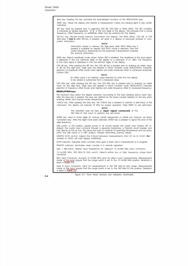
8/21/2019 HP5432 Microwave Frequency Counter
http://slidepdf.com/reader/full/hp5432-microwave-frequency-counter 34/364
Model 5342AOperation
3-6
Blue key. Pressing this key activates the blue-labeled functions of the RESOLUTION keys.
RESET key. Clears the display and restarts a measurement. Clears any blinking lights in key centerindicators.
SET key. Must be pressed prior to selecting OFS dB, OFS MHz or MAN (MHz). The SET conditionis indicated by lighted segments in the GHz digits of the display. This indicates that a centerfrequency, offset frequency, or amplitude offset may be entered into the display.
RECALL key. Recalls stored memory information into display. The MAN (MHz), OFS dB, or OFSMHz keys, if held in after RECALL is pressed, will result in a display of previously entered or com-puted information.
N O T E
Information stored in memory (by digit keys) after MAN (MHz) key ispressed is available for display until AUTO mode is selected. Then thecenter frequency determined by the automatic measurement overridesthe manual information.
AMPL key. Selects amplitude mode (when Option 002 is installed). The amplitude of the input signalis displayed in the four rightmost digits of the display to a resolution of 0.1 dBm. The frequencyof the input signal is displayed in the five leftmost digits of the display.
OFS dB key. After pressing the SET key, the OFS dB key is pressed prior to entering an offset valuein dB via the digit keys. (Digit keys are labeled in black numbers under RESOLUTION.) Indicatesselection of amplitude offset mode when lighted and adds amplitude offset to measured amplitude
(Option 002).N O T E
An offset value is an arbitrary value selected for entry into the displayto be added or subtracted from a measured value.
OFS MHz key. After pressing the SET key, the OFS MHz key is pressed prior to entering an offsetvalue via the digit keys. (Digit keys are labeled in black numbers under RESOLUTION.) Indicatesselection of frequency offset mode when lighted and adds frequency offset to measured frequency.
RESOLUTION keys:
The resolution keys select the display resolution (according to the blue labeling above each key)after the blue key is pressed. The keys are defined by the black number labeled on the key whenentering offsets and manual center frequencies.
CHECK key. After pressing the blue key, the CHECK key is pressed to perform a self-check of theinstrument. The display will indicate 75 MHz for proper operation. Press RESET to exit self-check.
N O T EThe instrument must not have an input signal connected at the500 MHz-18 GHz input to perform the self-check.
ENTER key. Used to enter digits for manual center frequencies or offsets into memory via black-numbered keys. After the digits have been selected, ENTER key is pressed to signal the end of thedigit sequence.
LINE switch. In ON position, applies power to all circuits except the crystal oven (Option 001 in-stalled). The crystal oven connects through a separate transformer, a thermal circuit breaker andfuse directly to the ac line. This allows the oven to maintain its operating temperature and accuracywhen the LINE switch is in STBY position, thereby eliminating warmup delays.
SAMPLE RATE control. Adjust s the in terval between measurements from 20 ms to HOLD. Whenrotated to HOLD will hold display indefinitely.
GATE indicator. Indicates when counters main gate is open and a measurement is in progress.
REMOTE indicator. Illuminates when counter is in remote operation.
50Ω− 1 ΜΩ switch. Selects input impedance for adjacent 10 Hz-500 MHz input connector.
10 Hz-500 MHz, 500 MHz-18 GHz switch. Selects either low or high frequency range inputconnector.
BNC Input Connector. Accepts 10 Hz-500 MHz input for direct count measurements. Measurementsmade at this input require that the range switch is set to the 10 Hz-500 MHz position. Sensitivity islisted in Table 1-1.
Type N Input Connector. Input for measurements in the 500 MHz-18 GHz range. Measurementsmade at this input require that the range switch is set to the 500 MHz-18 GHz position. Sensitivityis listed in Table 1-1.
Figure 3-1. Front Panel Controls and Indicators (Continued)

8/21/2019 HP5432 Microwave Frequency Counter
http://slidepdf.com/reader/full/hp5432-microwave-frequency-counter 35/364
Model 5342A
Operation
1.
2.
3.
4.
5.
6.
7.
8.
9.
10.
PROCESSOR INTERFACE connector A22W4JI. Not used. This connector is part of cable W4which is connected to A22 motherboard as an interface to the A14 Microprocessor address anddata lines. This interface is provided for future use with companion instruments.
position of digital input/output connector when instrument is equipped with Hewlett-PackardInterface Bus (HP-1B) Option 011. Refer to paragraph 3-69 for details.
Position of ADDRESS switch when instrument is equipped with Hewlett-Packard InterfaceBus (HP-IB) Option 011. Refer to paragraph 3-72 for details.
AC Power Module. Input power module consisting of an IEC approved connector, a fuse(0.75 amp for 100/200-volt operation, 0.375 for 220/240-volt operation) and a pC card linevoltage selector. Refer to paragraph 2-6 for details.
CW-FM selector switch. Selects a short or long pseudorandom sequence (prs). The CWposition provides a short prs (or narrow mode) with FM tolerance of 20 MHz p-p. The FMposition provides a long prs (or wide mode) with FM tolerance of 50 MHz p-p.
NOTE
Most measurements should be made with the rear panel FM/CWswitch in the CWposition. The FM posit ion should be used only whenthe input signal has significant amounts of FM (>20 MHz p-p).
lNT/EXT selector switch. Selects the internal 10 MHz crystal oscillator signal or an external10 MHz source for the time base circuit. The external source must be connected to the adjacentconnector (7).
NOTE
[f the lNT/EXT switch is switched and causes momentary loss of
clock, the microprocessor may hang up and cause the display to stopcounting. To recover, press LINE switch to STBY then to ON.
EXT FREQ STD connector. Accepts 10 MHz external time base signal when INT/EXT switchis in EXT position.
FREQ STD OUT connector. Supplies a 10 MHz squarewave output at 1.5 volts peak-to-peak.
IF OUT connector. provides the intermediate frequency (IF) output of the Preamplifier circuitfor test or monitor of the IF.
DAC connector. Provides the output voltage of the digital to analog converter when theOption 004 is installed.
Figure 3-2. Rear Panel Controls and Connectors 3-7

8/21/2019 HP5432 Microwave Frequency Counter
http://slidepdf.com/reader/full/hp5432-microwave-frequency-counter 36/364
Model 5342A
Operation
3-8
PRELIMINARY PROCEDURES
1. On rear panel:
a. Set lNT/EXT to INT position.
b. Set CW/FM switch to CW. Refer to paragraph 3-33 for detailed description.
c. On ac power module, check for proper fuse (0.75 amp for 100/120-volt operation, 0.375
amp for 220/240-voh operation) and check position of pc line voltage selector (refer toparagraph 2-6 for detailed description).
d. For remote operation, refer to paragraph 3-69 for explanation of HP-IB programming andaddress switch settings on rear panel (for 5342A’s equipped with Option 011).
2. On front panel, set LINE switch to ON position.
Do not exceed +25 dBm peak of input power at the type N con-
nector (500 MHz-18 GHz). Damage to the internal sampler may
occur.
NOTE
When the input signal level to the type N connector exceedsapproximately +5 dBm, each digit in the display becomes a minus
sign (-) to indicate overload. For Options 002,003, this threshold isapproximately +20 dBm.
The 10 Hz-500 MHz direct count input BNC connector is fuse-
protected for a maximum input level of 3.5V rms (+24 dBm).
NOTE
The fuse for the 10 Hz-500 MHz input is located on the A3 DirectCount Amplifier assembly.
Figure 3-3. Operating Procedures

8/21/2019 HP5432 Microwave Frequency Counter
http://slidepdf.com/reader/full/hp5432-microwave-frequency-counter 37/364
Model 5342A
Operation
3. Connect input signal to appropriate input connector according to frequency requirements(BNC for 10-500 MHz, type N for 500 MHz-18 GHz) and set frequency range switchaccordingly.
4. For input signals connected to BNC connector (10-500 MHz): set the 50Q-1 MQ switch asrequired. This switch has no effect on input signals connected to the type N connector (500MHz-18 GHz) .
5. Press blue key, then press blue-labeled RESOLUTION key for desired resolution.
NOTE
Half-sized are used as fillers in the display to facilitate displayinterpretation.
6. Adjust SAMPLE RATE control for desired interval between measurements.
KEY INDICATORS
Indicator LED’s in the center of some keys are used as “prompters”by the operator, as follows:
Blinking Indicator
A blinking LED in a key is a “ready” condition for that key function.It indicates it is waiting for an entry via the keyboard. To clear the con-
dition, press RESET.
Steady Indicator
A steady “on” LED in a key is an indication that the key function is ineffect. To clear the condition, press the key. (The AUTO Key is clearedby pressing MAN (MHz) and vice versa.)
SELF-CHECK PROCEDURE
Perform the self-check as follows (no input signal connected andSAMPLE RATE full CCW):
The manual center frequency is entered (and displayed) with 1 MHzresolution and must be within so MHz of the input signal frequency(connected to 500 MHz—18 GHz connector).
Figure 3-3. Operating Procedures (Continued)
3-9

8/21/2019 HP5432 Microwave Frequency Counter
http://slidepdf.com/reader/full/hp5432-microwave-frequency-counter 38/364
Model 5342A
Operation
3-10Figure 3-3. Operating Procedures (Continued)
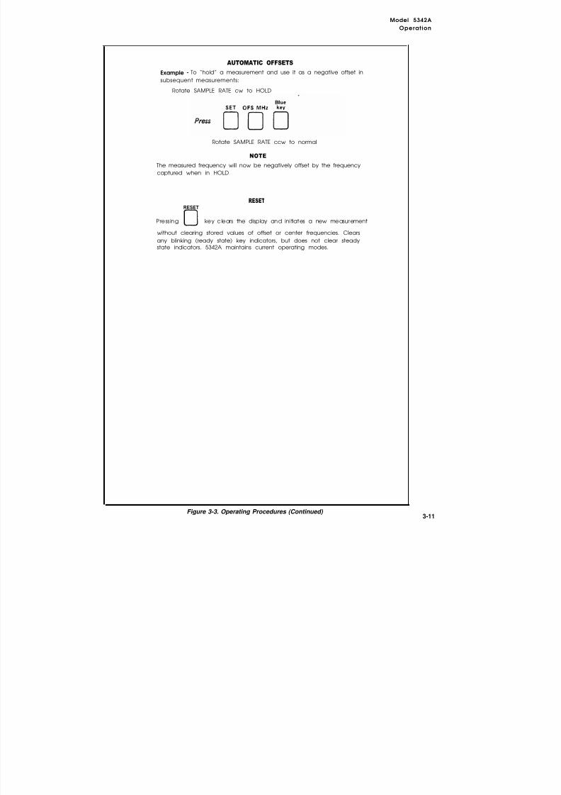
8/21/2019 HP5432 Microwave Frequency Counter
http://slidepdf.com/reader/full/hp5432-microwave-frequency-counter 39/364
Model 5342A
Operation
AUTOMATIC OFFSETS
Example - To “hold” a measurement and use it as a negative offset in
subsequent measurements:
Rotate SAMPLE RATE cw to HOLD
Rotate SAMPLE RATE ccw to normal
NOTE
The measured frequency will now be negatively offset by the frequencycaptured when in HOLD.
RESETRESET
Press ing key clears the display and initiates a new measurement
without clearing stored values of offset or center frequencies. Clearsany blinking (ready state) key indicators, but does not clear steadystate indicators. 5342A maintains current operating modes.
Figure 3-3. Operating Procedures (Continued) 3-11

8/21/2019 HP5432 Microwave Frequency Counter
http://slidepdf.com/reader/full/hp5432-microwave-frequency-counter 40/364
Model 5342A
Operation
3-12 Figure 3-4. Amplitude Measurements (Option 002)

8/21/2019 HP5432 Microwave Frequency Counter
http://slidepdf.com/reader/full/hp5432-microwave-frequency-counter 41/364
Model 5342A
Operation
Figure 3-5. DAC Operation (Option 004)
3-13

8/21/2019 HP5432 Microwave Frequency Counter
http://slidepdf.com/reader/full/hp5432-microwave-frequency-counter 42/364
3-45.
Model 5342AOperation
3-14

8/21/2019 HP5432 Microwave Frequency Counter
http://slidepdf.com/reader/full/hp5432-microwave-frequency-counter 43/364
Model 5342A Operation
3-15
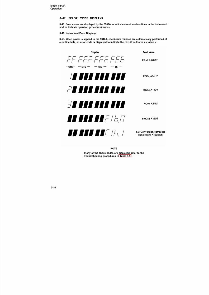
8/21/2019 HP5432 Microwave Frequency Counter
http://slidepdf.com/reader/full/hp5432-microwave-frequency-counter 44/364
Model 5342AOperation
3-47. ERROR CODE DISPLAYS
3-48. Error codes are displayed by the 5342A to indicate circuit malfunctions in the instrumentand to indicate operator (procedure) errors.
3-49. Instrument Error Displays
3-50. When power is applied to the 5342A, check-sum routines are automatically performed. ifa routine fails, an error code is displayed to indicate the circuit fault area as follows:
NOTE
If any of the above codes are displayed. refer to the
troubleshooting procedures in Table 8-5.
3-16

8/21/2019 HP5432 Microwave Frequency Counter
http://slidepdf.com/reader/full/hp5432-microwave-frequency-counter 45/364
3-52.
Model 5342AOperation
3-51. Operator Error Displays
3-17

8/21/2019 HP5432 Microwave Frequency Counter
http://slidepdf.com/reader/full/hp5432-microwave-frequency-counter 46/364
Model 5342AOperation
3-53. Limit Errors and Sequence Errors
3-54. A limit error (for example, setting a manual center frequency less than 500 MHz) will bedisplayed as:
3-55. A sequence error (for example, pressing a digit key before pressing a function key) will bedisplayed as:
3-56. For detailed descriptions of error codes, refer to Table 8-5.
3 - 5 7 . O P T I O N S
3-58, The operating characteristics of the 5342A are affected by the addition of any of theoptions described in the following paragraphs.
3-59. Time Base Option 001
3-60. Option 001 provides an oven-controlled crystal oscillator time base (Model 10544A) thatresults in higher accuracy and longer periods between calibration (refer to Table 1-1). The oventemperature is maintained when the 5342A LINE switch is in either the ON or the STBY position(provided the instrument is connected to the power mains). When the OVN indicator in thedisplay is lit, the oven is on (warming). When the oven is at the proper temperature, the OVNindicator goes out.
3-61. Amplitude Option 002
3-62. The amplitude option provides the capability of measuring the amplitude of the inputsignal and simultaneously displaying the frequency (5 leftmost digits) and the amplitude level indBm (4 rightmost digits). The maximum operating level of +5 dBm for the standard 5342A extended to +20 dBm for Option 002. The frequency is displayed to a resolution of 1 MHz and thelevel is displayed to a resolution of 0.1 dBm, The sensitivity of the 5342A with Option 002 isapproximately 3 to 5 dB less than the standard 5342A, depending upon frequency.
3-63. Extended Dynamic Range Option 003
3-64. The extended dynamic range option extends the maximum operating level of + 5 dBm forthe standard 5342A to +20 dBm for Option 003 by insertion of an attenuator at the input (ahead of
the sampler), The insertion loss of the attenuator results in a sensitivity decrease of approximately3 to 5 dB, depending upon the frequency of the signal.
3-65. HP-IB Interface Option 011
3-66. The Hewlett-Packard Interface Bus (HP-IB) Option 011 allows the functions of the 5342Ato be controlled remotely and allows measurement data to be ouptut to the bus, Programm-ing information for Option 011 is given in paragraphs 3-69 through 3-80.
3-18
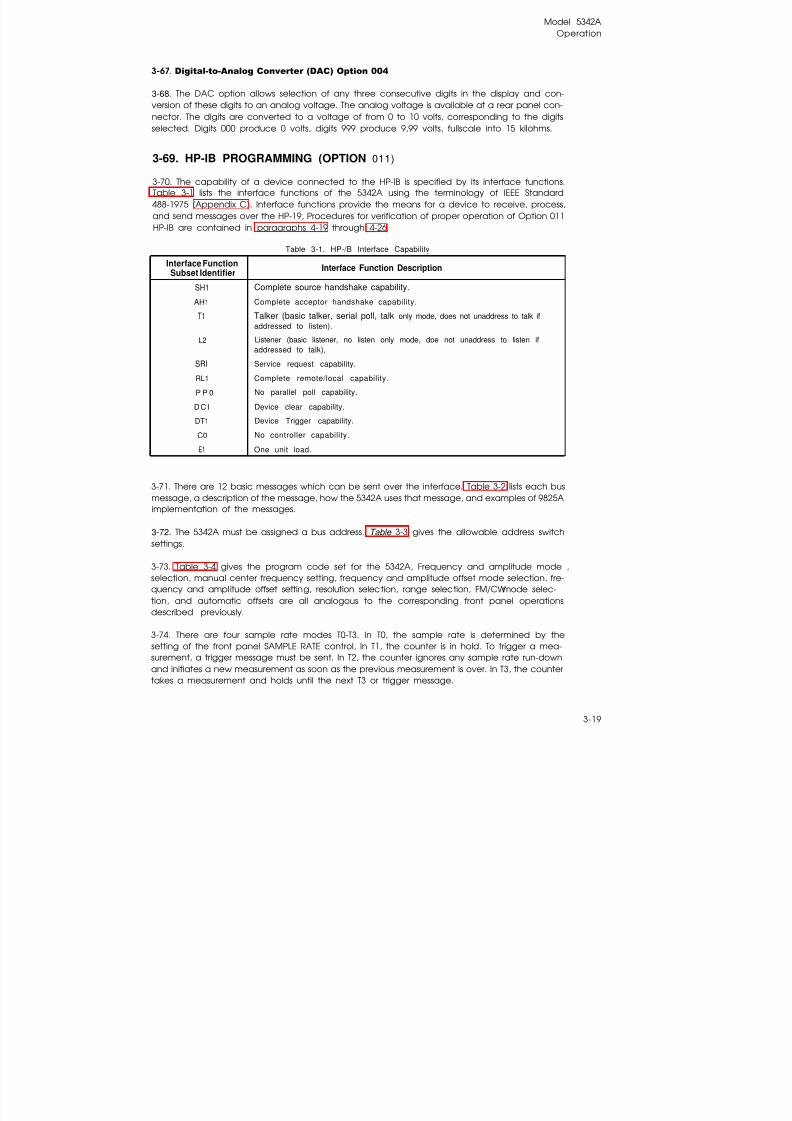
8/21/2019 HP5432 Microwave Frequency Counter
http://slidepdf.com/reader/full/hp5432-microwave-frequency-counter 47/364
Model 5342AOperation
3-67. Digital-to-Analog Converter (DAC) Option 004
3-68. The DAC option allows selection of any three consecutive digits in the display and con-version of these digits to an analog voltage. The analog voltage is available at a rear panel con-nector. The digits are converted to a voltage of from 0 to 10 volts, corresponding to the digitsselected. Digits 000 produce 0 volts, digits 999 produce 9,99 volts, fullscale into 15 kilohms.
3-69. HP-IB PROGRAMMING (OPTION 011)
3-70. The capability of a device connected to the HP-IB is specified by its interface functions.Table 3-1 lists the interface functions of the 5342A using the terminology of IEEE Standard488-1975 (Appendix C). Interface functions provide the means for a device to receive, process,and send messages over the HP-19, Procedures for verification of proper operation of Option 011HP-IB are contained in paragraphs 4-19 through 4-26.
Table 3-1. HP-/B Interface Capabilitv.
Interface FunctionSubset Identifier
Interface Function Description
SH1 Complete source handshake capability.
AH1 Complete acceptor handshake capability.
T1 Talker (basic talker, serial poll, talk only mode, does not unaddress to talk if
addressed to listen).
L2 Listener (basic listener, no listen only mode, doe not unaddress to listen if
addressed to talk),
SRI Service request capability.
RL1 Complete remote/local capability.
P P 0 No parallel poll capability.
DCI Device clear capability.
DT1 Device Trigger capability.
C0 No controller capability.
E1 One unit load.
3-71. There are 12 basic messages which can be sent over the interface. Table 3-2 lists each busmessage, a description of the message, how the 5342A uses that message, and examples of 9825Aimplementation of the messages.
3-72. The 5342A must be assigned a bus address. Table 3-3 gives the allowable address switchsettings.
3-73. Table 3-4 gives the program code set for the 5342A, Frequency and amplitude mode ,selection, manual center frequency setting, frequency and amplitude offset mode selection, fre-quency and amplitude offset setting, resolution selection, range selection, FM/CWmode selec-tion, and automatic offsets are all analogous to the corresponding front panel operations
described previously.
3-74. There are four sample rate modes T0-T3. In T0, the sample rate is determined by thesetting of the front panel SAMPLE RATE control, In T1, the counter is in hold. To trigger a mea-surement, a trigger message must be sent. In T2, the counter ignores any sample rate run-downand initiates a new measurement as soon as the previous measurement is over. In T3, the countertakes a measurement and holds until the next T3 or trigger message.
3-19

8/21/2019 HP5432 Microwave Frequency Counter
http://slidepdf.com/reader/full/hp5432-microwave-frequency-counter 48/364
Model 5342A
Operation
Table 3-2. 5342A Bus Message Usage
DescriptionSample 9825 Statements(5342A set to Address 02)
Message
Data
5342A Use
Transfers device-dependentinformation from one device toone or more devices on the bus.
Sends measurement data. Seeparagraph 3-77 for outputformat. Accepts program codes.See Table 3-4 for code set.
red 702, Awrt 702, “AUSR4”
Causes a group of selecteddevices to simultaneouslyinitiate a set of device-dependent actions
Causes an instrument to be set to
Starts a new measurement.Trigger
Clear
trg 7 o rtrg 702
Same as front panel RESET.Clears internal count and startsnew measurement.
clr 7 orclr 702a predefined state (a certain
range, function, etc.).
Permits selected devices to beset to remote operation, allow-ing parameters and device char-acteristics to be controlled byBus Messages.
Remote
Local
Local
Lockout
ClearLockout
and local
5342A goes to remote if REN istrue and addressed to listen. Inabsence of program data, re- rem 702mote operation is according tothe state of the front panel set-tings just prior to going toremote.
Goes to local front panel con-trol. In absence of front paneldata, local operation is accord-
Causes selected devices to re-turn to local (front panel)operation.
IcI 702
ing to the state of the remotedata just prior to going to local.
Disables front panel RESET.Disables local (front panel)controls of selected devices.
Returns all devices to local (frontpanel) control and simulta-neously clears the Local Lockout
l l o 75342A remains in remote.
Local lockout cleared and re- Icl 7turns to local front panel control
Message,
RequireService
StatusByte
Indicates a device’s need forinteraction with the controller.
Pulls on SRQ to indicate end of ameasurement.
rds(7)-Aif bit (7, A)
(bit 7=1 if SRQ true)
Presents status information of aparticular device; one bit indi-cates whether or not the devicecurrently requires service, theother 7 bits (optional) areused to indicate the type ofservice required.
In serial poll mode, 5342A out-puts decimal 80 (01010000) toindicate end of measurement,
rds (702)-A(if A=80, then 5342A is
ready to output)
Status Bit A single bit of device-dependentstatus information which may belogically combined with statusbit information from other de-vices by the controller.
Does not use
Passes bus controller responsi-bilities from the current con-troller to a device which canassume the Bus supervisory role.
Unconditionally terminates Bus
Pass
Control
Abort
Does not use
cli 7Clears Talk, Listen, Serial PollEnable registers on 5342A HP-IBinterface. Front panel annunci-ators do not change, however,
communications and returnscontrol to the system controller.
3 -20
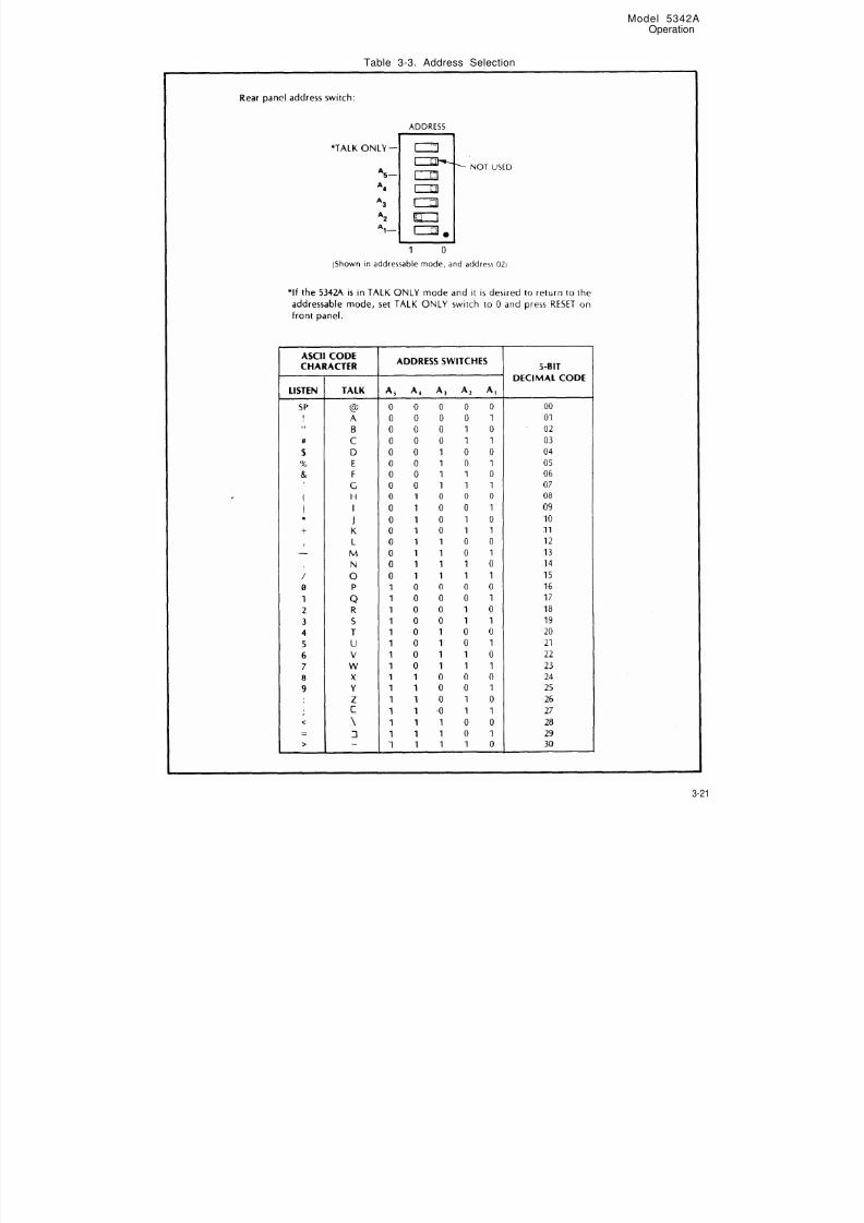
8/21/2019 HP5432 Microwave Frequency Counter
http://slidepdf.com/reader/full/hp5432-microwave-frequency-counter 49/364
Model 5342A Operation
Table 3-3. Address Selection
3-21

8/21/2019 HP5432 Microwave Frequency Counter
http://slidepdf.com/reader/full/hp5432-microwave-frequency-counter 50/364
Model 5342A
Operation
Table 3-4. Option 011 HP-IB Program Code Set
3-22

8/21/2019 HP5432 Microwave Frequency Counter
http://slidepdf.com/reader/full/hp5432-microwave-frequency-counter 51/364
Model 5342AOperation
Table 3-4. Option 011 HP-IR Program Code Set (Continued)
3-75. ln the“output only when addressed” mode, the counter pulls SRQ at the end of a mea-surement and then checks to see if it has been addressed to talk, If not, SRQ is cleared and it startsthe next measurement. If it has been addressed to talk, it outputs the measurement, clears SRQ,and-starts the next measurement. In the “wait until addressed” output mode, the counter pulls
SRQ at the end of a measurement and waits in a loop until it has been addressed to talk. When it is
addressed to talk, it outputs the measurement, clear SRQ and starts the next measurement,
N O T E
[f the counter is placed in the HOLD (T1) mode,triggered, then addressed to talk, be sure to use theWait Until Addressed (ST2) output mode. If not, thenfor short gate times the measurement may be com-pleted before the controller addresses the counter totalk and the counter will discard the measurementresult and hang up the bus.
3-76. The 5342A executes each complete program code as it is received just as if the micro-processor were receiving the data from the front panel keyboard, Program code strings should
be in the same order as they would be if being entered from the front panel. When a data byte issent to the 5342A HP-IB Option 011, the HP-IB interface stores the byte and sends an interrupt tothe microprocessor which reads in the byte. If the byte does not complete a program code, thenthe microprocessor waits for the next byte(s) until a complete code is sent (for example, SR5 is acomplete code but SR is not). After a complete code is received, the microprocessor executes thecode and begins the measurement. If more codes are in the string, another interrupt is gener-ated. For example, if the string “SR5AU” is sent by the controller, the “S” is the first byte receivedand stored by the 5342A HP-IB interface. The interface generates an interrupt to the micro-processor and the “S” is read by the MPU. Since S is not a complete code, the microprocessor
3-23

8/21/2019 HP5432 Microwave Frequency Counter
http://slidepdf.com/reader/full/hp5432-microwave-frequency-counter 52/364
paragraph 3-82.
Table 1-1.
3-77.
3-78.
Model 5342AOperation
waits until the complete code is sent and received. After “R” and then “5” are sent, the micro-processor sets the resolution accordingly and then goes to the beginning of the measurement.When the controller sends “A”, an interrupt is generated and “A” is read by the microprocessor.It then waits for the complete code to be sent which in this case is “AU”. The microprocessoragain goes to the start of the measurement cycle.
3-24
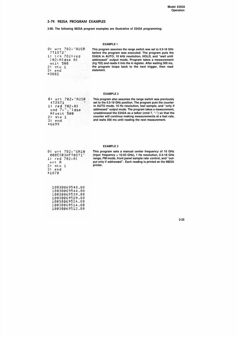
8/21/2019 HP5432 Microwave Frequency Counter
http://slidepdf.com/reader/full/hp5432-microwave-frequency-counter 53/364
Model 5342AOperation
3-79. 9825A PROGRAM EXAMPLES
3-80. The following 9825A program examples are illustrative of 5342A programming:
EXAMPLE 1This program assumes the range switch was set to 0.5-18 GHzbefore the program was executed. The program puts the5342A in AUTO, 10 kHz resolution, HOLD, and “wait untiladdressed” output mode. Program takes a measurement(trg 702) and reads it into the A register. After waiting 500 ms,the program loops back to the next trigger, then readstatement.
EXAMPLE 2
This program also assumes the range switch was previouslyset to the 0.5-18 GHz position. The program puts the counterin AUTO mode, 10 Hz resolution, fast sample, and “only ifaddressed” output mode. The program takes a measurement,unaddressed the 5342A as a talker (cmd 7, “-”) so that thecounter will continue making measurements at a fast rate,and waits 500 ms until reading the next measurement.
EXAMPLE 3
This program sets a manual center frequency of 10 GHz(input frequency = 10.03 GHz), 1 Hz resolution, 0.5-18 GHzrange, FM mode, front panel sample rate control, and “out-put only if addressed”. Each reading is printed on the 9825Aprinter.
3-25

8/21/2019 HP5432 Microwave Frequency Counter
http://slidepdf.com/reader/full/hp5432-microwave-frequency-counter 54/364
Model 5342A
Operation
EXAMPLE 4
This program selects AUTO mode, 1 Hz resolution, fastsample, “output only if addressed”, and amplitude “on”. Thefrequency is read into the A register and
-the amplitude is
read into the B register. Notice that although the frequencyis displayed only to 1 MHz resolution on the counter, the full1 Hz resolution is output to the calculator.
EXAMPLE 5
This program measures the same signal as in (4) but entersa -10 dB offset in the amplitude measurement.
3-26

8/21/2019 HP5432 Microwave Frequency Counter
http://slidepdf.com/reader/full/hp5432-microwave-frequency-counter 55/364
Model 5342AOperation
EXAMPLE 6
This is the same program as (5) but with a +10 GHz offset.
3-27

8/21/2019 HP5432 Microwave Frequency Counter
http://slidepdf.com/reader/full/hp5432-microwave-frequency-counter 56/364
Model 5342A
operation
3-81.
3-82.
a.
b.
c.
d.
HP-IB PROGRAMMING NOTES
The HP-IB output is affected by input signal level as follows:
For input signal levels greater than or equal to specified sensitivity, the 5342A outputsmeasurement data as described in paragraph 3-77.
For input signal levels less than the actual sensitivity by 0.1 dB or more (or for no input),
the counter outputs zeros when addressed to talk.
For input signal levels just on the edge of the ccunter’s actual sensitivity (approximately a 0.1 dB band) the detectors which indicate sufficient signal level for counting may becomeintermittent resulting in very long acquisition times. The counter’s display holds theprevious reading during the prolonged acquisition but the counter will not output anydata when addressed to talk. This will hang up the program at the read statement.
With the 9825A, use the “time” statement and “on err” statement to branch around theread statement if it takes longer than a specified number of milliseconds to complete an1/0 operation. The following example program can be used when there is more than on
read statement in the program. If there is only one read statement, then statement 2
could be deleted and the end of statement 7 could simply cause the program to go to thestatement after the read (in this case, “gto 6“):
Since this statement is in line 2, the
program jumps to the statement after
the read statement.
Error 4 is time out error. Reset timeand error jump.
When the 5342A took more time than
1 second to make the measurement,
zeroes are output.
3-28

8/21/2019 HP5432 Microwave Frequency Counter
http://slidepdf.com/reader/full/hp5432-microwave-frequency-counter 57/364
Model 5342AOperation
NOTE
For any controller, check SRQ to see if a measure-ment has been completed. Allow an adequatenumber of iterations on the SRC) check to permit thecounter to complete the measurement and pull SRQ.A flow diagram of such an algorithm is:
3-29

8/21/2019 HP5432 Microwave Frequency Counter
http://slidepdf.com/reader/full/hp5432-microwave-frequency-counter 58/364
Model 5342AOperation
3-83. REMOTE PROGRAMMING OF DIAGNOSTIC MODE 6(OPTION 002,011 ONLY)
3-84. In some system applications, it may be desirable to program the 5342A to diagnostic mode6 so that the counter wil l constantly present a low SWR and not switch to frequency measure-ments (higher SWR). The following example shows how this may be done:
EXAMPLE
— Program counter for AMPL mode
.
This sets the counter to diagnostic mode 6
Counter must be triggered to enter
‘diagnostic mode 6. For 5 seconds,
counter does not switch to frequency.
This resets the counter to amplitude and
frequency measurements
3-30
8/21/2019 HP5432 Microwave Frequency Counter
http://slidepdf.com/reader/full/hp5432-microwave-frequency-counter 59/364
Model 5342APerformance Tests
SECTION IVPERFORMANCE TESTS
4-1. INTRODUCTION
4-2. The procedures in this section test the electrical performance of the 5342A using the speci-fications in Table 1-1 as performance standards. Those specifications which are inherent to thedesign (obvious during operation) are not covered in these tests. For example, worst case acquisi-tion time is determined by the period of the sweep and the length of the pseudo-randomsequence. If the counter acquires the signal, it must have acquired it in a time less than specified.
4-3. OPERATIONAL VERIFICATION
4-4. The abbreviated checks given in paragraphs 4-12 through 4-18 can be performed to give ahigh degree of confidence that the 5342A is operating properly without performing the completeperformance test. The operational verification should be useful for incoming QA, routinemaintenance, and after instrument repair. The Option 011 HP-IB Verification Program is
described in paragraphs 4-19 through 4-26. The Option 004 DAC test is contained in para-graph 4-27.
4-5. COMPLETE PERFORMANCE TEST
4-6. The complete performance test is given in paragraphs 4-28 through 4-40. All tests can beperformed without access to the inside of the instrument.
4-7. EQUIPMENT REQUIRED
4-8. Equipment required for the complete test and operation verification is listed in Table 1-4.Any equipment which satisfies the critical specifications given in the table may be substituted forthe recommended model numbers.
4-9. TEST RECORD
4-10. Results of the operational verification may be tabulated on the Operational VerificationRecord, Table 4-1. Results of the performance test may be tabulated on the Performance TestRecord, Table 4-5.
4-1
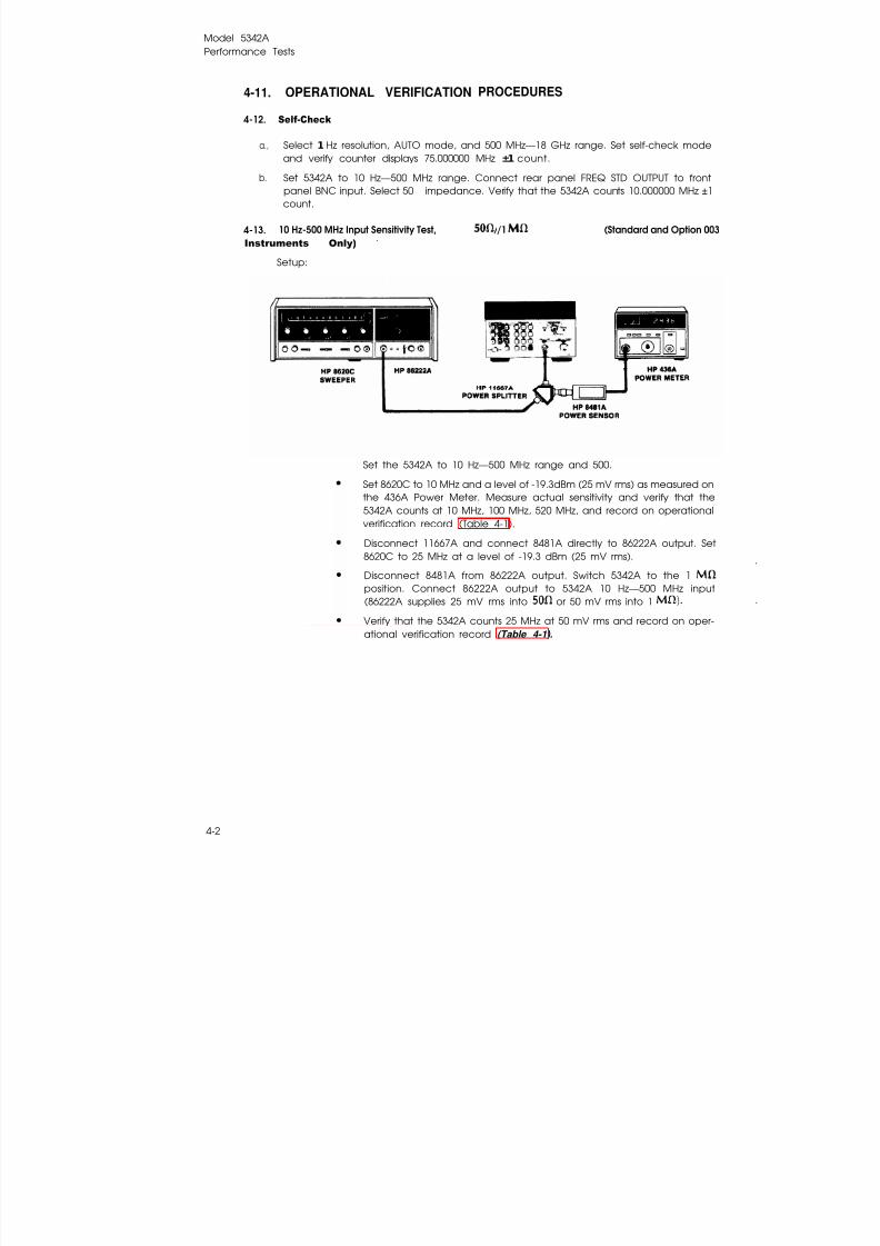
8/21/2019 HP5432 Microwave Frequency Counter
http://slidepdf.com/reader/full/hp5432-microwave-frequency-counter 60/364
Model 5342APerformance Tests
4-11.
4-12.
a.,
b.
4-13.
OPERATIONAL VERIFICATION
Self-Check
PROCEDURES
Select 1Hz resolution, AUTO mode, and 500 MHz—18 GHz range. Set self-check modeand verify counter displays 75.000000 MHz ±1 count.
Set 5342A to 10 Hz—500 MHz range. Connect rear panel FREQ STD OUTPUT to frontpanel BNC input. Select 50 impedance. Verify that the 5342A counts 10.000000 MHz ±1count.
10 Hz-500 MHz Input Sensitivity Test, /1 (Standard and Option 003
Instruments Only) -
Setup:
Set the 5342A to 10 Hz—500 MHz range and 500.
Set 8620C to 10 MHz and a level of -19.3dBm (25 mV rms) as measured onthe 436A Power Meter. Measure actual sensitivity and verify that the
5342A counts at 10 MHz, 100 MHz, 520 MHz, and record on operationalverification record (Table 4-1).
Disconnect 11667A and connect 8481A directly to 86222A output. Set8620C to 25 MHz at a level of -19.3 dBm (25 mV rms).
Disconnect 8481A from 86222A output. Switch 5342A to the 1 Mfl
position. Connect 86222A output to 5342A 10 Hz—500 MHz input(86222A supplies 25 mV rms into 50fl or 50 mV rms into 1 Mfl .
Verify that the 5342A counts 25 MHz at 50 mV rms and record on oper-ational verification record (Table 4-1) .
4-2

8/21/2019 HP5432 Microwave Frequency Counter
http://slidepdf.com/reader/full/hp5432-microwave-frequency-counter 61/364
Model 5342APerformance Tests
4-14. 10 Hz-500 MHz Input 500 Minimum Level and Amplitude Accuracy Test (Option 002)
Specification: ±1.5 dB accuracy for frequencies from 10 MHz to 520 MHz.
Minimum Level: -17 dBm.
Setup:
Connect the 11667A directly (using type N to BNC adapter) to the 5342ABNC low frequency input. Connect 8481A directly to the other 11667Aoutput.
Set the 5342A to 10 Hz-500 MHz range, 50Q, and amplitude mode.
Set the 86222A to 10 MHz and adjust output level and 8495B for a level of-17 dBm as measured on the 436A Power Meter. (8495B set to 10 dB orgreater.) Slowly vary the 8620C from 10 Hz to 520 MHz and verify that the5342A displays correct frequency.
Take a measurement at 10 MHz, 100 MHz, and 520 MHz, and verify that5342A reading is within ±1.5 dB of 436A reading. Enter results on oper-ational verification record (Table 4-1).
4-3

8/21/2019 HP5432 Microwave Frequency Counter
http://slidepdf.com/reader/full/hp5432-microwave-frequency-counter 62/364
Model 5342A
Performance Tests
4-15. 10 Hz-500 MHz Input(50Q)
Maximum Input Test (Option 002)
Specification: +20 dBm
Setup:
Set the 8495B to 10 dB,
Set the 3312A to 13 MHz sine wave with AMPLITUDE set to 10. Adjust
amplitude vernier for a +15 dBm output level (+5 dBm on 436A).
Set the 5342A to AMPL mode, 50Q, 10 Hz—500 MHz range and connect
the 3312A output to the 5342A input. Increase the 3312A output until
the 5342A measures +20 dBm.
Disconnect output of 3312A from 5342A and connect it to 8495B. Power
meter should display +10 dBm ±1.5dB (allowing for the + 10 dB of 8495 B).
Enter on operational verification record (Tabl e 4-1) .
Reconnect 3312A to 5342A and increase power output until 5342A
“dashes” the display to indicate overload. This must occur at a level
greater than +20 dBm. Enter on operational verification record.
4-4

8/21/2019 HP5432 Microwave Frequency Counter
http://slidepdf.com/reader/full/hp5432-microwave-frequency-counter 63/364
Model 5342APerformance Tests
4-16. 500 MHz—18 GHz Input Sensitivity Test (Standard and Option 003 Instruments Only)
Specification: Sensitivity = -25 dBm, 500 MHz-12.4 GHz= -20 dBm, 12.4 GHz-18 GHz.
For Option 003:
Sensitivity = -22 dBm, 500 MHz-12.4 GHz
= -15 dBm, 12.4 GHz-18 GHz.Description: The 5342A is set to the 500 MHz-18 GHz range and a signal at the rated
sensitivity is applied to the type N connector. The frequency is slowlyvaried over the range of 500 MHz to 12.4 GHz and the 5342A is checkedfor proper counting. The output level of the test generator is increased tothe second value, the frequency is slowly varied from 12.4 GHz to 18GHz, and the 5342A checked for proper counting.
Set the 5342A to the 500 MHz-18 GHz range.
Connect the 11667A Power Splitter directly to the 5342A type N connec-tor. Connect the 8481A power sensor directly to the other output port ofthe 11667A power splitter.
Set the 8620C with the appropriate plug-in (86222A for 500 MHz to 2 GHz,86290A for 2 GHz-18 GHz) and the 8495B step attenuator to the ratedsensitivity as measured on the 436A. Remember that the 5342A with
Option 003 has different specifications.
Slowly increase the 8620C frequency over the range and verify that the5342A counts properly.
Measure actual sensitivity at 1 GHz,12.4GHz, and 18GHz. Enter on oper-ational verification record (Table 4-1).
4-5
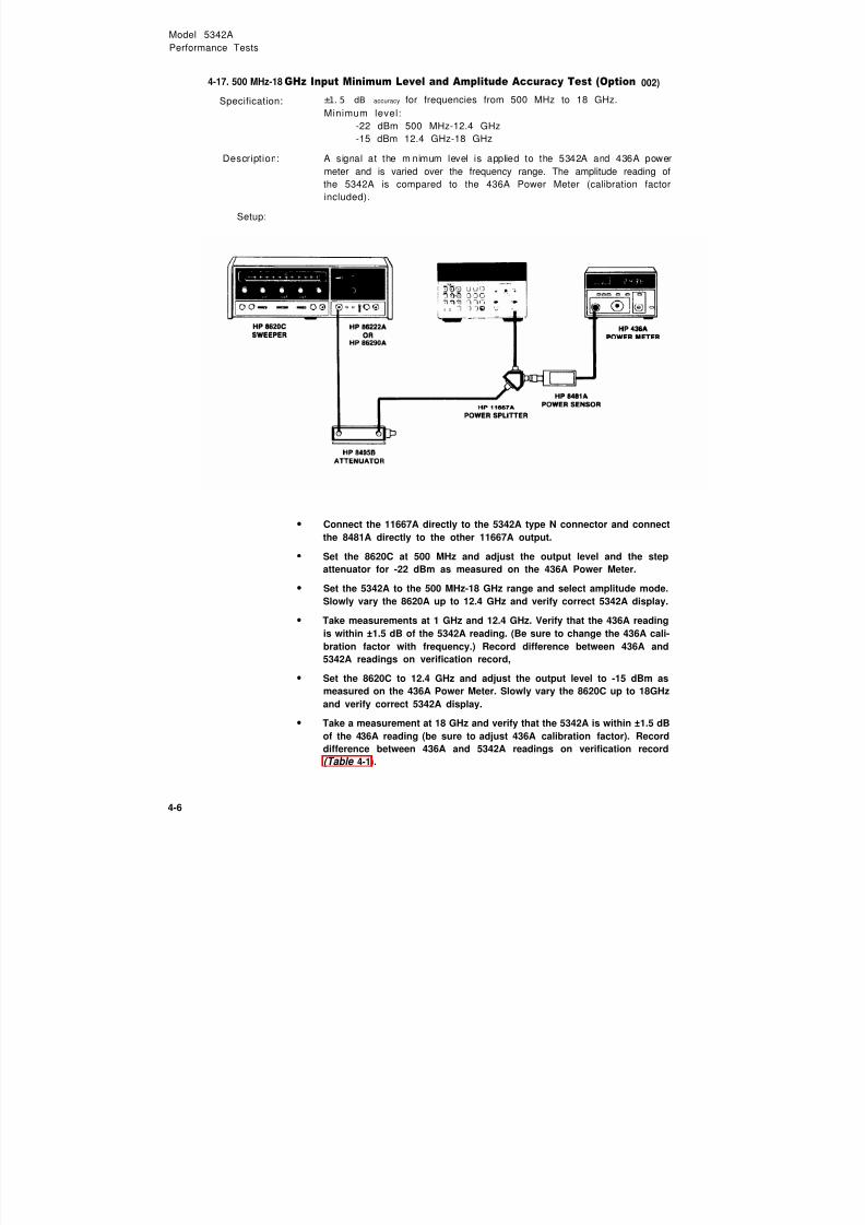
8/21/2019 HP5432 Microwave Frequency Counter
http://slidepdf.com/reader/full/hp5432-microwave-frequency-counter 64/364
Model 5342A
Performance Tests
4-17. 500 MHz-18 GHz Input Minimum Level and Amplitude Accuracy Test (Option
Specification: ±1. 5 dB accuracy for frequencies from 500 MHz to 18 GHz.
Minimum level:
-22 dBm 500 MHz-12.4 GHz
-15 dBm 12.4 GHz-18 GHz
002)
Description: A signal at the minimum level is applied to the 5342A and 436A power
meter and is varied over the frequency range. The amplitude reading of
the 5342A is compared to the 436A Power Meter (calibration factor
included).
Setup:
Connect the 11667A directly to the 5342A type N connector and connect
the 8481A directly to the other 11667A output.
Set the 8620C at 500 MHz and adjust the output level and the step
attenuator for -22 dBm as measured on the 436A Power Meter.
Set the 5342A to the 500 MHz-18 GHz range and select amplitude mode.
Slowly vary the 8620A up to 12.4 GHz and verify correct 5342A display.
Take measurements at 1 GHz and 12.4 GHz. Verify that the 436A reading
is within ±1.5 dB of the 5342A reading. (Be sure to change the 436A cali-
bration factor with frequency.) Record difference between 436A and
5342A readings on verification record,
Set the 8620C to 12.4 GHz and adjust the output level to -15 dBm as
measured on the 436A Power Meter. Slowly vary the 8620C up to 18GHz
and verify correct 5342A display.
Take a measurement at 18 GHz and verify that the 5342A is within ±1.5 dB
of the 436A reading (be sure to adjust 436A calibration factor). Record
difference between 436A and 5342A readings on verification record
(Table 4-1).
4-6

8/21/2019 HP5432 Microwave Frequency Counter
http://slidepdf.com/reader/full/hp5432-microwave-frequency-counter 65/364
Model 5342APerformance Tests
4-18. 500 MHz-18 GHz High Level Test
For Standard Instrument:
Set the 8620C to 1 GHz at +5.0 dBm as measured by the 436A PowerMeter. Connect the 8620C output to the 5342A and verify that thecounter counts 1 GHz.
Increase the level of the 8620C output until the counter’s display fills withdashes. Measure this level on the 436A and verify that it is greater than+5 dBm. Enter on verification record (Table 4-1).
.For Option 002 Instruments:
Set 5342A to 500 MHz-18 GHz range and AMPL mode.
Set the 8620C to 1 GHz at a level of +10 dBm as measured on the 436A.
Connect the 8620C output to the 5342A and verify that the 5342A counts1 GHz. Enter difference between 5342A and 436A readings on verifi-cation record (Table 4-1).
4-19. OPTION 011 HP-IB VERIFICATION PROGRAM
4-20. The 9825A program listed in Table 4-2 exercises the 5342A through various operatingmodes, described below, via its HP-IB Interface. If the 5342A successfully completes all phases of
the verification program, then there is a high probability that the HP-IB Interface (A15 assembly)is working properly. If the 5342A does not respond as described, refer to HP-IB troubleshootingin Section VIII.
NOTE
Prior to conducting the performance test, check theA15 board revision letter (adjacent to the board partnumber). If the revision letter is D or later, check theLSRQ line to pin 13 to be sure the jumper is installedas shown in Figure 8-38.
4-7

8/21/2019 HP5432 Microwave Frequency Counter
http://slidepdf.com/reader/full/hp5432-microwave-frequency-counter 66/364
Model 5342APerformance Tests
4-21. To perform the verification, set up the 5342A as shown and set its rear panel addressswitches to address 07.
4-22. The program listed in Table 4-2 may be keyed into the 9825A or may be loaded from a
HP-IB Verification Cassette, HP P/N 59300-10001, (Revision B or Iater] which also contains HP-IBverification programs for the 59300 series of instruments. To run the program on the cassette,insert the cassette into the 9825A, load file 0, and press RUN. Enter “5342” when the instrumentmode number is requested and select code “707” when select code is requested. The 9825A willthen load the 5342A verification program into memory.
4-23. Apply power to the 5342A and verify that the counter powers up in AUTO mode andREMOTE off. Verify that when the range switch is placed in the 10 Hz-500 MHz position andimpedance select to 50 the counter counts its 10 MHz time base.
4-24. The program goes through 14 check points for the standard instrument and an additional4 check points for the amplitude option (002). The information in Table 4-3 tells what occursduring each test and what should be observed by the operator if the test has been successfully
completed. At the conclusion of each test, the program stops and displays the current checkpoint. To advance to the next test, simply press CONTINUE. If it is desired to repeat a test, set thevariable Lto 1 via the keyboard (1--L EXECUTE), To go on to the next test after looping, set L backto when the program halts L (EXECUTE). Record on operational verification record(Table 4-1).
4-25. When the 9825A displays “AMPL OPT?” at the end of check point 14, enter “YES” if the5342A has Option 002. Enter “NO” if the amplitude option is not present.
4-26. Table 4-4 is a sample printout from the 9825A.
4-8

8/21/2019 HP5432 Microwave Frequency Counter
http://slidepdf.com/reader/full/hp5432-microwave-frequency-counter 67/364
Table 4-1.
4-12
4-13
4-14
4-16
4-17
4-18
4-19
4-26
4-27
Model 5342APerformance Tests
4-9
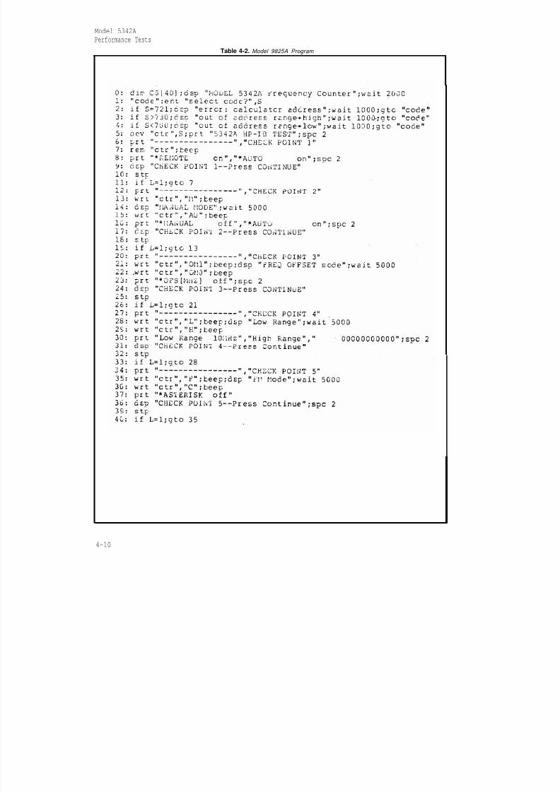
8/21/2019 HP5432 Microwave Frequency Counter
http://slidepdf.com/reader/full/hp5432-microwave-frequency-counter 68/364
Model 5342A
Performance Tests
Table 4-2. Model 9825A Program
4-10
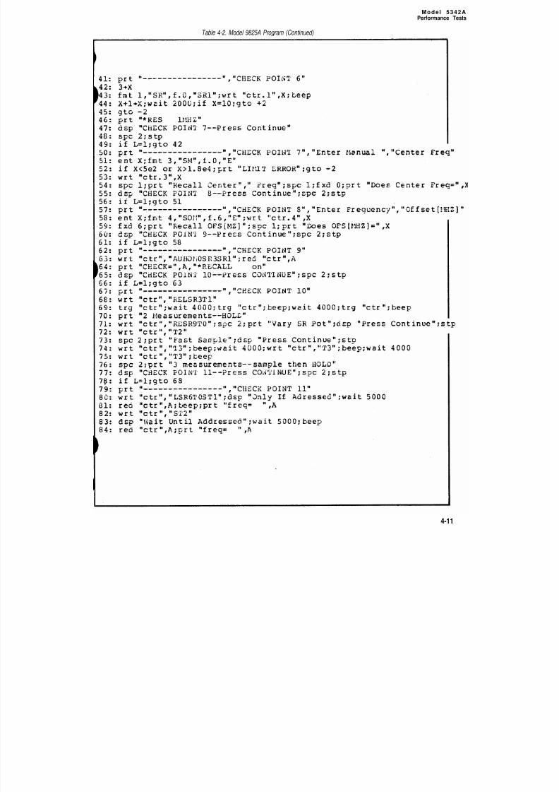
8/21/2019 HP5432 Microwave Frequency Counter
http://slidepdf.com/reader/full/hp5432-microwave-frequency-counter 69/364
Mode l 5 3 4 2 APerformance Tests
Table 4-2. Model 9825A Program (Continued)
4-11
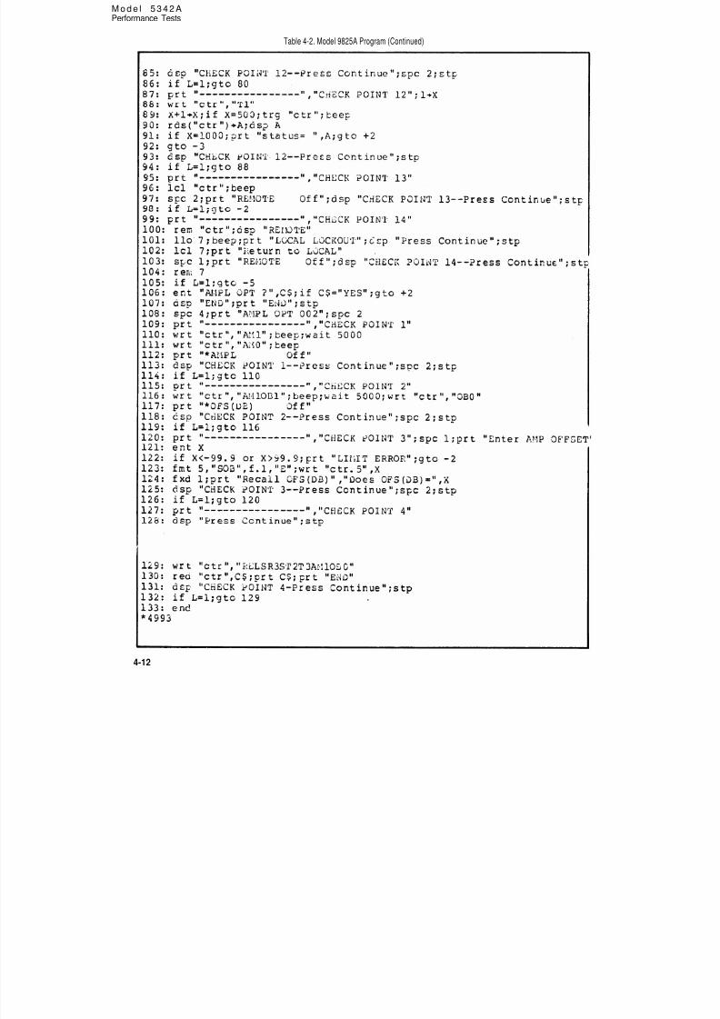
8/21/2019 HP5432 Microwave Frequency Counter
http://slidepdf.com/reader/full/hp5432-microwave-frequency-counter 70/364
M o d e l 5 3 4 2 APerformance Tests
Table 4-2. Model 9825A Program (Continued)
4-12
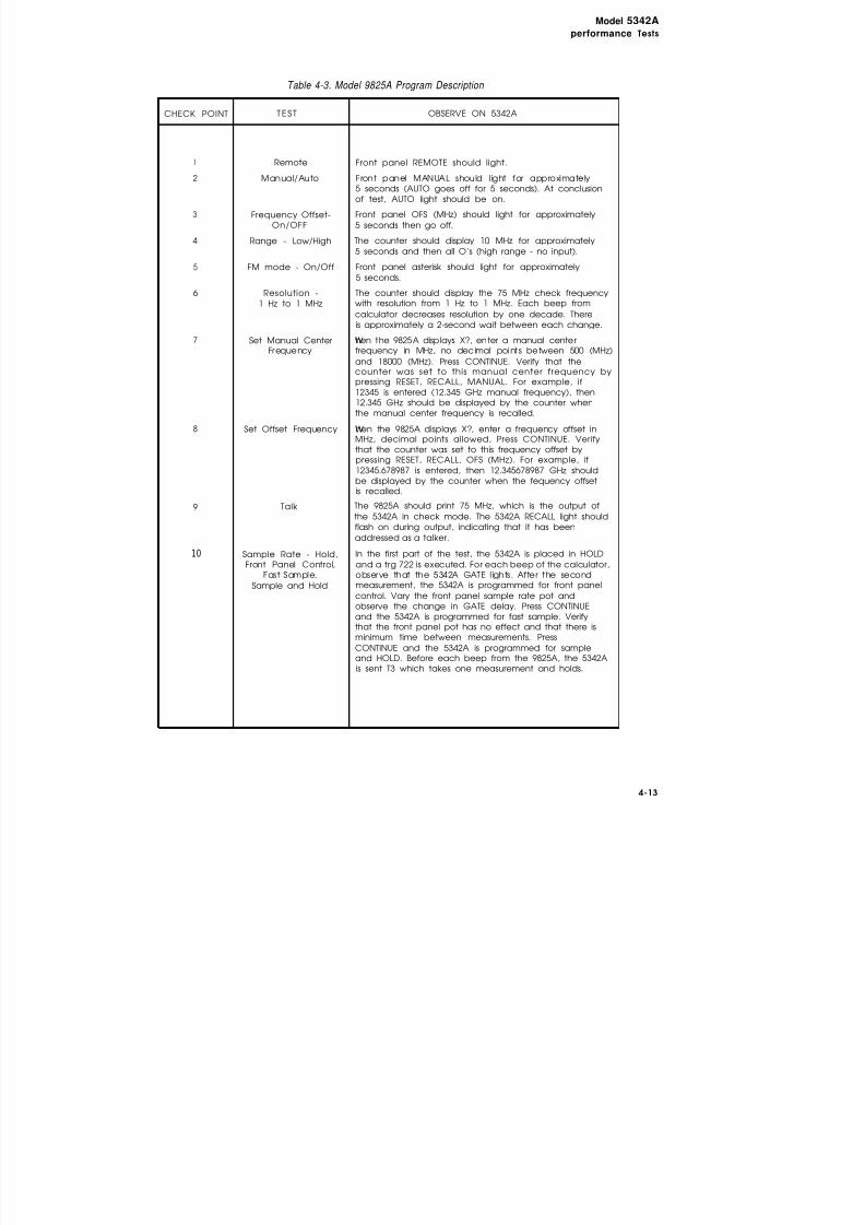
8/21/2019 HP5432 Microwave Frequency Counter
http://slidepdf.com/reader/full/hp5432-microwave-frequency-counter 71/364
Model 5342Aperformance Tests
Table 4-3. Model 9825A Program Description
CHECK POINT T E S T OBSERVE ON 5342A
1 Remote Front panel REMOTE should light.2 Manual/Auto Front panel MANUAL should l ight for approximately
5 seconds (AUTO goes off for 5 seconds). At conclusionof test, AUTO light should be on.
3 Frequency Offset- Front panel OFS (MHz) should light for approximatelyOn/OFF 5 seconds then go off.
4 Range - Low/High The counter should display 10 MHz for approximately5 seconds and then all O’s (high range - no input).
5 FM mode - On/Off Front panel asterisk should light for approximately5 seconds.
6 Resolution - The counter should display the 75 MHz check frequency1 Hz to 1 MHz with resolution from 1 Hz to 1 MHz. Each beep from
calculator decreases resolution by one decade. Thereis approximately a 2-second wait between each change.
7 Set Manual Center When the 9825A displays X?, enter a manual centerFrequency frequency in MHz, no decimal points between 500 (MHz)
and 18000 (MHz). Press CONTINUE. Verify that thecounter was set to this manual center frequency bypressing RESET, RECALL, MANUAL. For example, if12345 is entered (12.345 GHz manual frequency), then12.345 GHz should be displayed by the counter whenthe manual center frequency is recalled.
8 Set Offset Frequency When the 9825A displays X?, enter a frequency offset inMHz, decimal points allowed, Press CONTINUE. Verifythat the counter was set to this frequency offset bypressing RESET, RECALL, OFS (MHz). For example, if12345.678987 is entered, then 12.345678987 GHz shouldbe displayed by the counter when the fequency offsetis recalled.
9 Talk The 9825A should print 75 MHz, which is the output ofthe 5342A in check mode. The 5342A RECALL light shouldflash on during output, indicating that it has beenaddressed as a talker.
10 Sample Rate - Hold, In the first part of the test, the 5342A is placed in HOLDFront Panel Control, and a trg 722 is executed. For each beep of the calculator,
Fast Sample, observe that the 5342A GATE l ights. After the secondSample and Hold measurement, the 5342A is programmed for front panel
control. Vary the front panel sample rate pot andobserve the change in GATE delay. Press CONTINUEand the 5342A is programmed for fast sample. Verifythat the front panel pot has no effect and that there isminimum time between measurements. PressCONTINUE and the 5342A is programmed for sampleand HOLD. Before each beep from the 9825A, the 5342Ais sent T3 which takes one measurement and holds.
4-13

8/21/2019 HP5432 Microwave Frequency Counter
http://slidepdf.com/reader/full/hp5432-microwave-frequency-counter 72/364
Model 5342A
Performance Tests
Tab le 4-3. Model 9825A Program Description (Continued)
CHECK POINT T E S T OBSERVE ON 5342A
11 Only If/Wait At the start of this test, the 5342A is placed in the ONLYUntil Addressed IF addressed mode. The GATE light should continually
light, indicating that measurements are continuallybeing made until the 5342A is addressed to talk. Thecounter is addressed to talk and the value is printed,The counter is then placed in WAIT UNTIL addressed,The GATE light should go out after the first measure-ment and remain out, indicating that the first measure-ment is being saved until the counter is addressed totalk. It is then addressed to talk and the value is printedby the printer,
12 Status Byte The 5342A is put in HOLD and serial poll mode. Itsstatus byte is displayed by the 9825A. After approxi-
mately 5 seconds, the 5342A is triggered and a measure-ment is taken. The status byte displayed by the 9825Ashould change from O to 80, indicating that the 5342Ahas taken a measurement.
13 Go To Local LCL 722 is issued. The front panel REMOTE light shouldgo off.
14 Local Lockout The 5342A is returned to remote control and the locallockout command is issued, When the 9825A displays“press CONTINUE”, press RESET on the 5342A andverify that the counter remains in REMOTE. PressCONTINUE on the 9825A and Icl 7 is issued. Verify thatthe 5342A goes to local.
AMPLOPTION 002:
1Amplitude-On/Off Front panel AMPL should light for approximately 5seconds and then of off.
2 Amplitude Offset- Front panel OFS (dB) should light for approximatelyOn/Off 5 seconds and then go off.
3 Set Amplitude When the 9825A displays X?, enter an amplitude offsetOffset in dB in the range of -99.9 to +99.9. Press CONTINUE.
Verify that the 5342A was set to this offset by pressingRESET, RECALL, OFS (dB).
4 AMPL Output The 5342A is placed in amplitude mode and addressedto talk, Verify proper output format as given in sampleprintout in Tab/e 4-4.
4-14

8/21/2019 HP5432 Microwave Frequency Counter
http://slidepdf.com/reader/full/hp5432-microwave-frequency-counter 73/364
Model 5342A
Performance Tests
Table 4-4. Sample Printout
4-15

8/21/2019 HP5432 Microwave Frequency Counter
http://slidepdf.com/reader/full/hp5432-microwave-frequency-counter 74/364
Model 5342APerformance Tests
4-27. DIGITAL-TO-ANALOG CONVERTER (DAC) OUTPUT TEST (OPTION 004)
Specification: Accuracy = ±5 mV, ±0.3 mV/°C (from 25°C).
Description: The 5342A is set to the 500 MHz-18 GHz range and a 999 MHz signal is
applied to the type N connector. A DVM is connected to the DAC OUTconnector on the rear panel. The front panel keyboard is used to selectdigits 999 and the DVM observed for an indication of 9.99 volts dc. Then
the 000 digits are selected and the DVM observed for 0 volts dc.
Setup:
Set the 5342A to the 500 MHz-18 GHz range, AUTO mode.
Connect DVM to DAC OUT, set DVM to 20V range.
Set the generator to 999 MHz as indicated on 5342A display.
On 5342A keyboard, press:
Observe DMV for indication of 9.99 ±0.01. Enter on operational verifi-
cation record (Table 4-7).
On 5342A keyboard, press:
Observe DVM for 0 ±0.01. Enter on operational verification record.On 5342A keyboard, press:
Observe DVM for 9.00 ±0.01. Enter on performance test record.
4-16

8/21/2019 HP5432 Microwave Frequency Counter
http://slidepdf.com/reader/full/hp5432-microwave-frequency-counter 75/364
Model 5342APerformance Tests
TEST PROCEDURES4-28. PERFORMANCE
4-29. 10 Hz-500 MHz Input Sensitivity Test, 500 (Standard and Option 003 Instruments Only)
Specification: 50 position, sensitivity = 25 mV rms for frequencies from 10 Hz-520MHz .
Description: The 5342A is set to the 10 Hz-500 MHz range and a signal at the ratedsensitivity is applied to the BNC input. The frequency is slowly swept upto 10 MHz at constant level and the 5342A reading is checked for theproper count. For the range of 10 MHz to 520 MHz, a different generatoris used. For Option 002, sensitivity is tested in paragraph 4-37.
Setup:
a. 10 Hz—10 MHz
Set 651B to 10 Hz and 25 mV rms.
Increase the frequency of the 651B and verify that the 5342A countsproper frequency from 10 Hz to 10 MHz.
Measure actual sensitivity by decreasing the 651B level until the 5342Agives an unstable count at these frequencies: 10 Hz, 1 kHz, 500 kHz,5 MHz, 10 MHz. Enter on performance test record ( Table 4-1).
b. 10 MHz-520 MHz
5342A settings remain unchanged.
Set 436A power meter for AUTO range and dBm mode. Set the 86222A for INT leveling and adjust the output power level for a
436A reading of -19.3 dBm (25 mV rms into 500).
Increase the frequency of the 8620C over the range of 10 MHz to 520MHz and verify that the 5342A counts proper frequency. Use 436A toverify input power.
Measure actual sensitivity at 50 MHz, 250 MHz, 520 MHz, and enter onperformance test record (Table 4-5).
4-17

8/21/2019 HP5432 Microwave Frequency Counter
http://slidepdf.com/reader/full/hp5432-microwave-frequency-counter 76/364
Model 5342A
Performance Tests
4-30. 10 Hz-500 MHz Input Sensitivity Test, 1M
Specifications: 1 M position, sensitivity = 50 mV rms for frequencies from 10 Hz-
25 MHz.
Setup:
a. 10 Hz-10 MHz
Set the 651B to 10 Hz and adjust level for 141 mV p-p signal (50 mV rms).
Increase the frequency of the 651B and verify that the 5342A counts
proper frequency from 10 Hz to 10 MHz.
Measure actual sensitivity at 10Hz, 1kHz, 500kHz,5MHz, and 10MHz by
monitoring p-p voltage on oscilloscope. Enter on performance test
record (Table 4-5).
b. 10 MHz-25 MHz
5342A settings remain unchanged.
Adjust 86222A output for a 141 mV p-p (50 mV rms) reading on the 1740A.
Increase the frequency of the 8620C from 10 MHz-25 MHz and verify
that the counter counts properly. Monitor the output level on the oscil-
loscope for 141 mV p-p (50 mV rms) over the range.
Measure actual sensitivity at 15 MHz, 25 MHz, and enter on performance
test record (Table 4-5) .
4-18

8/21/2019 HP5432 Microwave Frequency Counter
http://slidepdf.com/reader/full/hp5432-microwave-frequency-counter 77/364
Model 5342A
Performance Tests
4-31. 500 MHz-18 GHz Input Sensitivity Test (Standard and Option 003 Instruments Only)
Specification: Sensitivity = -25 dBm, 500 MHz-12.4 GHz
= -20 dBm, 12.4 GHz-18 GHz
For Option 003:
Sensitivity = -22 dBm, 500 MHz-12.4 GHz
= -15 dBm, 12.4 GHz-18 GHz
Description: The 5342A is set to the 500 MHz-18 GHz range and a signal at the rated
sensitivity is applied to the type N connector. The frequency is slowly
varied over the range of 500 MHz to 12.4 GHz and the 5342A is checked
for proper counting. The output level of the test genertor is increased to
the second value, the frequency is slowly varied from 12.4 GHz to 18
GHz, and the 5342A
sensitivity is tested in
checked for proper counting. For Option 002,
paragraph 4-37.
Setup:
Set the 5342A to the 500 MHz-18 GHz range, AUTO mode.
Connect the 11667A power splitter directly to the 5342A type N connec-
tor. Connect the 8481A power sensor directly to the other output port of
the 11667A power splitter.
Set the 8620C with the appropriate plug-in (86222A for 500 MHz to 2GHz,
86290A for 2 GHz-18 GHz) and the 8495B step attenuator to the ratedsensitivity as measured on the 436A. Remember that the 5342A with
Option 003 has different specifications.
Slowly increase the 8620C frequency over the range and verify that the
5342A counts properly.
Measure actual sensitivity at 500 MHz, 1 GHz, 5 GHz, 10 GHz, 12.4 GHz,
15 GHz, 17 GHz, and 18 GHz. Enter on performance test record
(Table 4-5).
4-19

8/21/2019 HP5432 Microwave Frequency Counter
http://slidepdf.com/reader/full/hp5432-microwave-frequency-counter 78/364
Model 5342A
Performance Tests
4-32. 500 MHz-18 GHz Input SWR Test
Specification: <2:1 500MHz-10GHz
<3:1 10 GHz-18 GHz
Option 002: <2:1 500 MHz-18 GHz (during amplitude measurements)5:1 500 MHz-18GHz (during frequency measurements)
Option 003: <5:1 500 MHz-18 GHz
Description: Using an 8755B Swept Amplitude Analyzer, the return loss of the 5342A
high frequency input is measured over the range of 2GHZ to 18GHz. An
SWR of 2:1 (9.5dB return loss) is worst case for frequencies below 10GHz
and an SWR of 3:1 (6 dB return loss) is worst case for frequencies from 10GHz-18 GHz. The dual directional coupler outputs the incident powerand reflected power to the 11664A detectors. The 8755B performs theratio and displays return loss directly.
Setup:
4-20

8/21/2019 HP5432 Microwave Frequency Counter
http://slidepdf.com/reader/full/hp5432-microwave-frequency-counter 79/364
Model 5342APerformance Tests
Set the 8620C to sweep from 2 GHz to 18 GHz with the FAST vernier setfull clockwise.
Set the 86290A to the 2-18GHz band and a power level of approximately+5 dBm, internally leveled.
Set the 8755B for SMOOTHING (ON), OFFSET CAL (ON), DISPLAY (A/R),THUMBWHEELS (ØØ), scale 5 dB/div. Set the 182T to EXT CAL.
To calibrate the 8755B, short (or open) the 11692D coupler output whichfeeds the 5342A. Adjust the OFFSET CAL of the A channel to center thescope display at the center horizontal line of the 182T CRT.
Connect 5342A to 11692D coupler and set A channel offset dB on the8755B to -09. The trace should be below the center line for frequenciesbelow 10 GHz as shown below. Verify that the return loss is >9.5dB from2-10 GHz and >6.0 dB from 10-18 GHz (standard instrument). ForOption 003, verify that the return loss is >3.5 dB over the range of 2-18GHz. Enter the minimum return loss for each range of frequency on theperformance test record (Table 4-5).
FOR AMPLITUDE OPTION, put the 5342A in diagnostic mode 5 (pressSET, SET 5) to prevent switching between the sampler input and the peakdetector input. Measure SWR as described above and verify that for
amplitude measurements, return loss is >9.5 dB for frequencies from 2GHz-18 GHz. Next put the 5342A in AUTO and frequency only so thatamplitude measurements are not made. Verify that the return loss is >3.5dB for frequencies from 2-18 GHz (SWR <5:1).
4-21

8/21/2019 HP5432 Microwave Frequency Counter
http://slidepdf.com/reader/full/hp5432-microwave-frequency-counter 80/364
Model 5342APerformance Tests
4-33. 500 MHz-18 GHz Maximum Input Test
Specification: +5 dBm (Standard Instrument)+20 dBm (Options 002, 003)
Description: The 5342A display will fill with dashes in an overload condition. Thedetecting circuits controlling the “dashing” of the display exhibitapproximately 2 dB hysteresis so that once the threshold is exceeded, the
level must be dropped by approximately 2 dB before the counter willcount again. Consequently, it is critical that in this test the level beapproached from below the +5 dBm limit. Since the sampler response isgreatest near 1 GHz, this test is made at 1 GHz.
Setup:
The standard instrument is tested first and then the Option 002 or 003,
(which use a thin film attenuator in front of the sampler to increase themaximum allowable input to +20 dBm) is tested (if installed).
(Standard Instrument)
Set the 8620C to 1 GHz at +5.0 dBm as measured by the 436A PowerMeter. Connect the 8620C output to the 5342A and verify that thcounter counts 1 GHz,
Increase the level of the 8620C output until the counter’s display fills withdashes, Measure this level on the 436A and verify that it is greater than +5,dBm, Enter the level (at which the display is dashed) on the performancetest record (Table 4-5).
4-22

8/21/2019 HP5432 Microwave Frequency Counter
http://slidepdf.com/reader/full/hp5432-microwave-frequency-counter 81/364
Model 5342APerformance Tests
For Options 002 003 only:
Set the 84956 to 10 dB.
Set the 8620C to 1 GHz and connect the 84956 output to the 8481A powersensor. Adjust the 489A gain control and 86222A gain control for a 489Aoutput level of +15 dBm (+5 dBm displayed on 436A).
Connect the 489A output to the 5342A and verify that the counter counts1 CHz. Increase the signal level until 5342A (Option 002) displays +20dBm ±1.5 dB. Enter on performance test record, Reconnect signal to5342A and increase level until display fills with dashes. This must occur ata level >+20 dBm. Enter the level (at which the display is dashed) on theperformance test record (Table 4-5), Be sure to add 10 dB to 436Areadings to account for the 8495B attenuator.,
4-23

8/21/2019 HP5432 Microwave Frequency Counter
http://slidepdf.com/reader/full/hp5432-microwave-frequency-counter 82/364
Model 5342APerformance Test s
4-34. FM Tolerance Test
Specification: 20 MHz peak-to-peak (CWmode)50 MHz peak-to-peak (FM mode)
Description: The FM tolerance specification indicates the worst case FM deviationwhich can be present on a carrier that the counter can acquire andcount. If the deviations are symmetrical about the carrier, then the
counter averages out the deviations and displays the carrier frequency.
A rear panel switch controls the CWmode and FM mode,
In this test, a function generator is used to FM the 8620C and the output isexamined on a spectrum analyzer to measure the peak-to-peak devi-ation. The amplitude of the modulating waveform is adjusted for a 20MHz p-p deviation and then a 50 MHz-p-p deviation.
Set 86290A to 4 GHz at -10 dBm.
Put 5342A in 500 MHz-18 GHz range and AUTO mode. Observe IF Oon the spectrum analyzer. Set 5342A to manual mode to setup peak-to-peak deviation,
4-24

8/21/2019 HP5432 Microwave Frequency Counter
http://slidepdf.com/reader/full/hp5432-microwave-frequency-counter 83/364
Model 5342APerformance Tests
Apply modulating signal to EXT FM input on the rear panel of 86290A.Use a 100 kHz sine wave of sufficient amplitude to give 20 MHz p-p FMdeviation as shown. (Modulating rate for this photo was 100 kHz.) Recordon performance test record (Table 4-5).
Switch the counter from manual to AUTO to verify that the counter willacquire and count the signal.
If deviations are symmetrical about center frequency, the 5342A willaverage out the deviations and display the 4.0 GHz center frequency.
Return the MAN mode, Increase amplitude of modulating waveform toproduct a 50 MHz p-p deviation as shown below (fm = 100 kHz). Recordon performance test record (Table 4-5).
Switch rear panel switch to FM. Switch counter from MAN to AUTO.
Verify that the counter will acquire and count the signal.
If deviations are symmetrical about the center frequency, the 5342A willaverage out the deviations and display the 4.0 GHz center frequency. Forthis case, the deviation is not symmetrical about the center frequency, Toverify that the counter has passed the test, check that the displayed fre-quency is within 300 MHz of 4 GHz (if then N number computed is off by1 due to excessive FM, then the displayed frequency will be off by 300 to350 MHz).
4-25
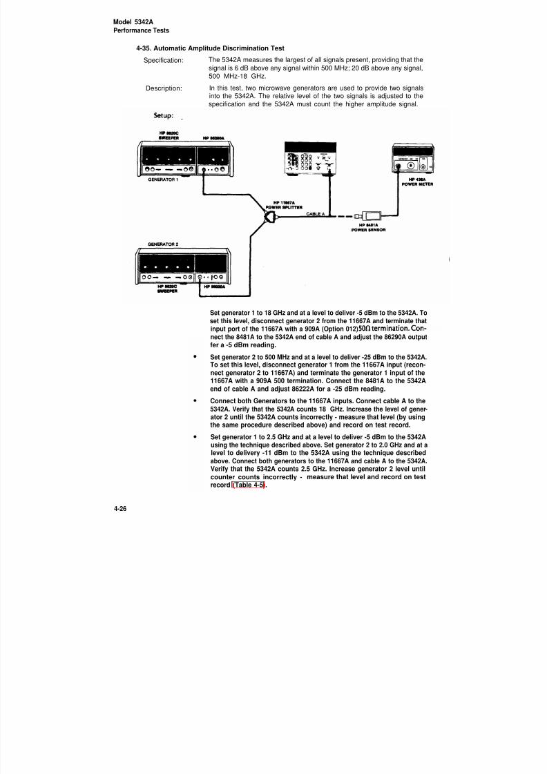
8/21/2019 HP5432 Microwave Frequency Counter
http://slidepdf.com/reader/full/hp5432-microwave-frequency-counter 84/364
Model 5342A
Performance Tests
4-35. Automatic Amplitude Discrimination Test
Specification: The 5342A measures the largest of all signals present, providing that the
signal is 6 dB above any signal within 500 MHz; 20 dB above any signal,
500 MHz-18 GHz.
Description: In this test, two microwave generators are used to provide two signalsinto the 5342A. The relative level of the two signals is adjusted to the
specification and the 5342A must count the higher amplitude signal.
Set generator 1 to 18 GHz and at a level to deliver -5 dBm to the 5342A. Toset this level, disconnect generator 2 from the 11667A and terminate thatinput port of the 11667A with a 909A (Option 012)
nect the 8481A to the 5342A end of cable A and adjust the 86290A outputfer a -5 dBm reading.
Set generator 2 to 500 MHz and at a level to deliver -25 dBm to the 5342A.To set this level, disconnect generator 1 from the 11667A input (recon-nect generator 2 to 11667A) and terminate the generator 1 input of the11667A with a 909A 500 termination. Connect the 8481A to the 5342Aend of cable A and adjust 86222A for a -25 dBm reading.
Connect both Generators to the 11667A inputs. Connect cable A to the5342A. Verify that the 5342A counts 18 GHz. Increase the level of gener-
ator 2 until the 5342A counts incorrectly - measure that level (by usingthe same procedure described above) and record on test record.
Set generator 1 to 2.5 GHz and at a level to deliver -5 dBm to the 5342Ausing the technique described above. Set generator 2 to 2.0 GHz and at alevel to delivery -11 dBm to the 5342A using the technique describedabove. Connect both generators to the 11667A and cable A to the 5342A.Verify that the 5342A counts 2.5 GHz. Increase generator 2 level untilcounter counts incorrectly - measure that level and record on test
record (Table 4-5).
4-26

8/21/2019 HP5432 Microwave Frequency Counter
http://slidepdf.com/reader/full/hp5432-microwave-frequency-counter 85/364
Model 5342A
Performance Tests
4-36. 500 MHz-18 GHz Input Minimum Level and Amplitude Accuracy Test (Option 002)
Specification: ±1.5 dB accuracy for frequencies from 500 MHz to 18 GHz
Minimum level:
-22 dBm 500 MHz-12.4 GHz
-15 dBm 12.4 GHz-18 GHz
Description: A signal at the minimum level is applied to the 5342A and 436A Power
Meter and is varied over the frequency range. The amplitude reading ofthe 5342A is compared to the 436A Power Meter (calibration factor
included).
Connect the 11667A directly to the 5342A type N connector and connect
the 8481A directly to the other 11667A output.
Set the 8620C at 500 MHz and adjust the output level and the step attenu-
ator for -22 dBm as measured on the 436A Power Meter (8495B set for atleast 10 dB).
Set the 5342A to the 500 MHz-18GHz range and select amplitude mode.
Slowly vary the 8620C up to 12.4 GHz and verify that the 5342A counts
correctly.
Take measurements at 500 MHz, 1 GHz, 5 GHz, 10 GHz, 12.4 GHz. Verify
that the 436A reading is within ±1.5 dB of the 5342A reading. (Be sure to
change the 436A calibration factor with frequency. ) At each frequency,
increase level by taking out 10 dB in the 8495B attenuator and verify that
the readings agree within ±1.5 dB. Record the actual 5342A amplitude
readings on the performance test record ( Table 4-5) .
Set the 8620C to 12.4 GHz and adjust the output level to -15 dBm as mea-
sured on the 436A Power Meter. Slowly vary the frequency to 18 GHz and
verify that the 5342A counts correctly.
Take measurements at 12.4 GHz, 15 GHz, 17 GHz, 18GHz, and verify that
the 5342A is within ±1.5 dB of the 436A reading (be sure to adjust 436A
calibration factor). At each frequency, increase level by reducing 8495B
by 10 dB and verify that readings again agree within ±1.5 dB. Record the
actual amplitude readings on the performance test record (Table
4-5) .
4-27

8/21/2019 HP5432 Microwave Frequency Counter
http://slidepdf.com/reader/full/hp5432-microwave-frequency-counter 86/364
Model 5342A
Performance Tests
4-37. 10 Hz-500 MHz Input Minimum Level and Amplitude Accuracy Test (Option 002)
Specification: ±1.5 dB accuracy for frequencies from 10 MHz to 520 MHz
Minimum Level: -17 dBm.
Setup:
Connect the 11667 directly (using type N to BNC adapter) to the 5342A
BNC low frequency input. Connect 8481A directly to the other 11667A
output.
Set the 5342A to 10 Hz-500 MHz range,
Set the 86222A to 10 MHz and adjust output level and 8495B for a level of
-17 dBm as measured on the 436A Power Meter. (84956 set to 10 dB or
greater.)
Take a measurement at 10 MHz, 5 MHz, 100 MHz, 300 MHz, 520 MHz,
and verify that 5342A reading is within ±1.5 dB of 436A reading. At each
frequency, increase level by taking out 10 dB in the 8495B and verify that
readings agree to within ±1.5 dB, Record the actual 5342A amplitude
measurements on the performance test record (Table 4-5).
4-28

8/21/2019 HP5432 Microwave Frequency Counter
http://slidepdf.com/reader/full/hp5432-microwave-frequency-counter 87/364
Model 5342A
Performance Tests
4-38. 10 Hz-500 MHz Input 50Q) Maximum Input Test (Option 002)
Specification: +20 dBm
Setup:
Set the 8495B to 10 dB.
Set the 3312A to 13 MHz sine wave with AMPLITUDE set to 10. Adjust
amplitude vernier for a +15 dBm output level (+5 dBm on 436A).
Set the 5342A to AMPL mode, 50fl, 10 Hz-500 MHz range and connect
the 3312A output to the 5342A input. Increase the 3312A output until the
5342A measures +20 dBm.
Disconnect output of 3312A from 5342A and connect it to 8495B. Power
meter should display +10 dBm ±1.5 dB (allowing for the +10 dB of 8495 B).Record on performance test record (Table 4-5).
Reconnect 3312A to 5342A and increase power output until 5342A
“dashes” the display to indicate overload. This must occur at a level
greater than +20 dBm. Record this level on performance test record
(Table 4-5).
4-29

8/21/2019 HP5432 Microwave Frequency Counter
http://slidepdf.com/reader/full/hp5432-microwave-frequency-counter 88/364
Model 5342APerformance Tests
4-39. 10 Hz-500 MHz Input (50f2) SWR Test (Option 002)
Specification: <1.8:1
Description: Using a lower frequency range directional coupler (such as the 778 D),the test setup described in paragraph 4-13 is used to sweep the low fre-quency input over the range of 100 MHz to 500MHz and the return loss ismeasured. Return loss must be >10.75 dB over the range.
Setup:
Same as described in paragraph 4-32 except use the 86222A plug-in and
setup to sweep from 100 MHz to 500 MHz. Replace the 11692D DualDirectional Coupler with the 778D Dual Directional Coupler.
Calibrate the system with a short (or open) at the 778D output which
normally feeds the 5342A low frequency input, Set the 5342A to 50Q and diagnostic mode 5 (described in Table 8-8) to
prevent switching between frequency and amplitude measurements.Verify that the return loss is >10,75 dB, Record on performance test
record (Table 4-5) .
4-30

8/21/2019 HP5432 Microwave Frequency Counter
http://slidepdf.com/reader/full/hp5432-microwave-frequency-counter 89/364
Model 5342A
Performance Tests
Description:
4-40. Digital-to-Analog Converter (DAC) Output Test (Option 004)
Specification: Accuracy = ±5 mV, ±0.3 mV/°C (from 25°C)
The 5342A is set to the 500 MHz-18 GHz range and a 999 MHz signal is
applied to the type N connector. A DVM is connected to the DAC OUT
connector on the rear panel. The front panel keyboard is used to selectdigits 999 and the DVM observed for an indication of 9.99 volts dc. Then
the 000 digits are selected the DVM observed for 0 volts dc.
Setup:
Set the 5342A to the 500 MHz-18 GHz range, AUTO mode.
Connect DVM to DAC OUT, set DVM to 20V range.
Set the generator to 999 MHz as indicated on 5342A display.
Observe DVM for indication of 9.99 ±0.01. Enter on performance test
record (Table 4-5) .
On 5342A keyboard, press:
Observe DVM for Ø ± 0.01. Enter on performance test record (Table
4-5).
Observe DVM for 9.00 ±0.01. Enter on performance test record ( Tabl e 4-5) .,
4-31

8/21/2019 HP5432 Microwave Frequency Counter
http://slidepdf.com/reader/full/hp5432-microwave-frequency-counter 90/364
4-29
4-32
4-30
4-31
4-33
4-34
4-35
Model 5342APerformance Tests
Table 4-5. Performance Test Record
4-32
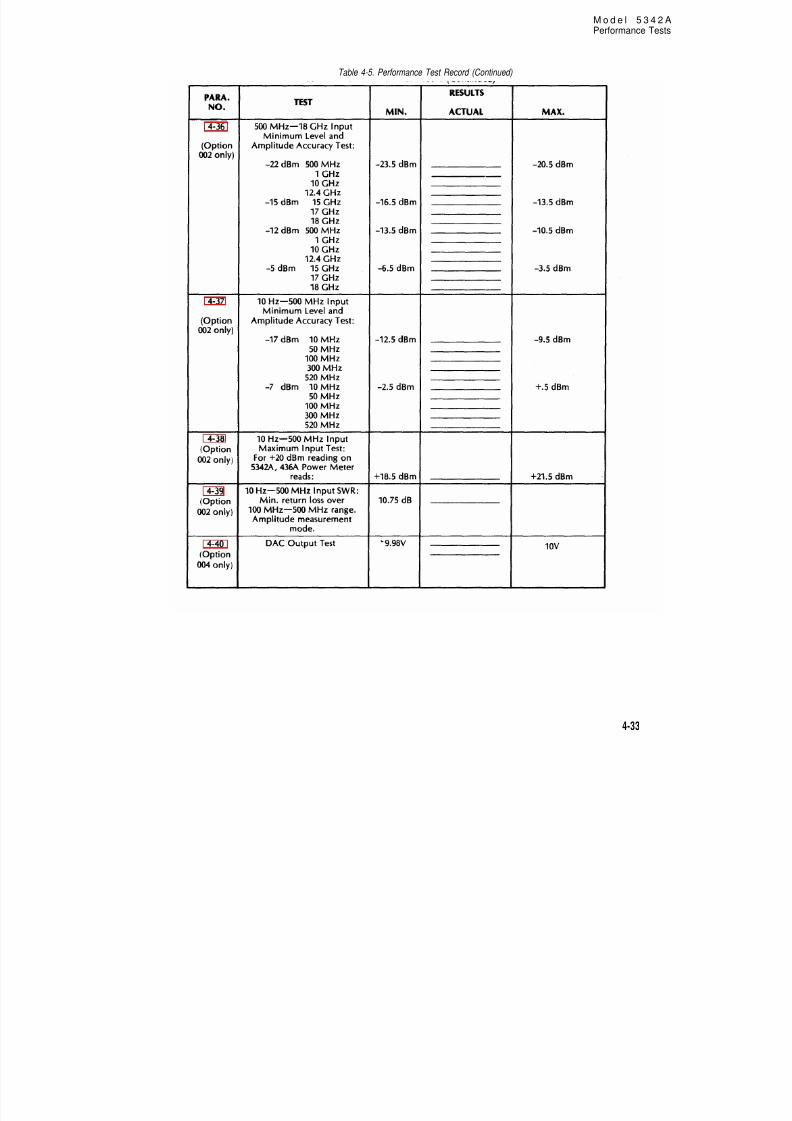
8/21/2019 HP5432 Microwave Frequency Counter
http://slidepdf.com/reader/full/hp5432-microwave-frequency-counter 91/364
4-36
4-37
4-38
4-39
4-40
M o d e l 5 3 4 2Performance Tes
Table 4-5. Performance Test Record (Continued)
4-33
8/21/2019 HP5432 Microwave Frequency Counter
http://slidepdf.com/reader/full/hp5432-microwave-frequency-counter 92/364
Model 5342A
Adjustments
SECTION V
ADJUSTMENTS
5 - 1 . I N T R O D U C T I O N
5-2. This section describes the adjustments required to maintain the 5342A’s operating charac-teristics within specifications. Adjustments should be made when required, such as after a per-
formance test failure or when components are replaced that may affect an adjustment.
5-3. Table 5-1 is a list of all adjustable components in the 5342A and indicates the order in which
adjustments should be performed.
5 - 4 . E Q U I P M E N T R E Q U I R E D
5-5. The test equipment required for the adjustment procedures is listed in Table 1-4, Re-
commended Test Equipment. Substitute instruments may be used if they meet the critical
specifications.
5 - 6 . F A C T O R Y S E L E C T E D C O M P O N E N T S
5-7. Factory selected components are identified by an asterisk (*) in parts lists and schematic
diagrams. Refer to paragraph 8-36 for replacement information.
5 - 8 . A D J U S T M E N T L O C A T I O N S
5-9. Adjustment locations are identified in the component locators in the Section VIII sche-
matic diagrams and in the top view of the instrument, Figure 8-21.
5 - 1 0 . S A F E T Y C O N S I D E R A T I O N S
5-11. This section contains warnings that must be followed for your protection and to avoid
damage to the equipment.
WARNING
MAINTENANCE DESCRIBED HEREIN IS PERFORMED
WITH POWER SUPPLIED TO THE INSTRUMENT,AND PROTECTIVE COVERS REMOVED. SUCH
MAINTENANCE SHOULD BE PERFORMED ONLY BYSERVICE-TRAINED PERSONNEL WHO ARE AWAREOF THE HAZARDS INVOLVED (FOR EXAMPLE, FIREAND ELECTRICAL SHOCK). WHERE MAINTENANCECAN BE PERFORMED WITHOUT POWER APPLIED,THE POWER SHOULD BE REMOVED.
BEFORE ANY REPAIR IS COMPLETED, ENSURE THATALL SAFETY FEATURES ARE INTACT AND FUNC-
TIONING, AND THAT ALL NECESSARY PARTS ARECONNECTED TO THEIR PROTECTIVE GROUNDINGMEANS.
5-1
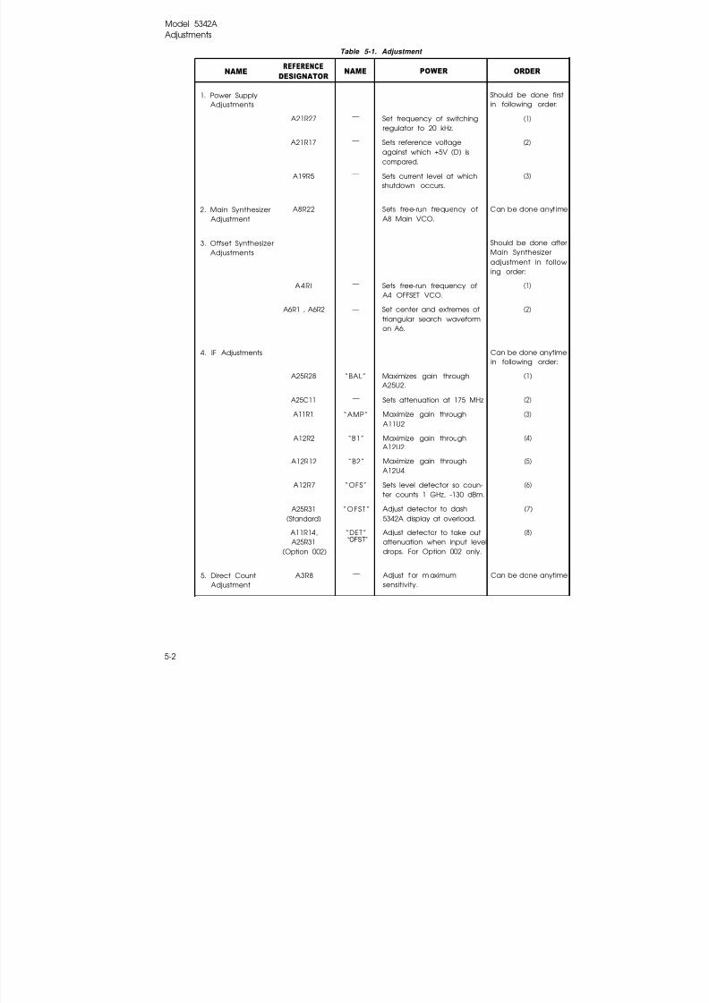
8/21/2019 HP5432 Microwave Frequency Counter
http://slidepdf.com/reader/full/hp5432-microwave-frequency-counter 93/364
Model 5342A
Adjustments
Table 5-1. Adjustment
NAMEREFERENCE
DESIGNATORNAME POWER ORDER
1. Power Supply Should be done firstAdjustments in following order:
A21R27 — Set frequency of switching (1)
regulator to 20 kHz.
A21R17 — Sets reference voltage (2)
against which +5V (D) iscompared.
A19R5 — Sets current level at which (3)
shutdown occurs.
2. Main Synthesizer A8R22 — Sets free-run frequency of Can be done anytimeAdjustment A8 Main VCO.
3. Offset Synthesizer Should be done afterAdjustments Main Synthesizer
adjustment in follow
ing order:A4RI — Sets free-run frequency of (1)
A4 OFFSET VCO.
A6R1 , A6R2 — Set center and extremes of (2)
triangular search waveformon A6.
4. IF Adjustments Can be done anytimein following order:
A25R28 “BAL” Maximizes gain through (1)
A25U2.
A25C11 — Sets attenuation at 175 MHz (2)
A11R1 “AMP” Maximize gain through (3)
A11U2.
A12R2 “B1” Maximize gain through (4)A12U2.
A12R12 “B2” Maximize gain through (5)
A12U4.
A12R7 “OFS” Sets level detector so coun- (6)
ter counts 1 GHz, -130 dBm.
A25R31 “OFST” Adjust detector to dash (7)
(Standard) 5342A display at overload.
A11R14, “DET” Adjust detector to take out (8)
A25R31“OFST”
attenuation when input level(Option 002) drops. For Option 002 only.
5. Direct Count A3R8 — Adjust f or m aximum Can be done anytimeAdjustment sensitivity.
5-2

8/21/2019 HP5432 Microwave Frequency Counter
http://slidepdf.com/reader/full/hp5432-microwave-frequency-counter 94/364
Model 5342A
Adjustments
Table 5-1. Adjustment (Continued)
NAMEREFERENCE
DESIGNATORNAME PURPOSE ORDER
6. Amplitude Can be done any-Adjustments time in following(Option 002) order:
A16R21 — Adjusts reference voltage to (1)
3.200 volts for ADC on A16.
A16R29 — Adjust loop gain. Set the volt- (2)age into the ADC for a specifiedlevel of 100 kHz.
A16R26 — Adjust dc offset. Set the voltage (3)into the ADC for a specifiedlevel of 100 kHz.
A27R9 “CAL” Adjusts the output of the (4)
100 kHz detector on A27.
A27R10 “High Level Cal’’Adjusts the output of the (5)100 kHz detector on A27 forhigh levels.
7. Digital-to- A2R25 GAIN Adjust maximum (9.99V) DAC Can be doneAnalog (DAC) output. anytimeAdjustments A2R27 OFFSET Adjusts minimum (0V) DAC
(Option 004) output.
5-12. ADJUSTMENT PROCEDURES
5-13. Power Supply Adjustments
5-14. Adjust resistor A21R27 (20 kHz frequency) as follows:
a. Place A21 on extender board. Monitor A21TP2 with an oscilloscope.
b. Adjust A21R27 (bottom, right side pot) for a 50 µS ±1 µs period as shown:
c. Replace A21 in instrument,
5-3

8/21/2019 HP5432 Microwave Frequency Counter
http://slidepdf.com/reader/full/hp5432-microwave-frequency-counter 95/364
Model 5342AAdjustments
5-15. Adjust resistor A21R17, +5V (D) as follows:
With a 3465A Multimeter in the DAC VOLTS FUNCTION and 20V range, measure the dcvoltage of the -5.2V supply at XA21(5,5). Adjust A21 R17 for a -5.20 (-0.1, +0.05)V dc.
WARNING
PRIOR TO MAKING ANY VOLTAGE TESTS ON THEA19 PRIMARY POWER ASSEMBLY, THE VOLTMETERTO BE USED OR THE 5342A MUST BE ISOLATEDFROM THE POWER MAINS BY USE OF AN lSOLA-
TION TRANSFORMER. A TRANSFORMER SUCH ASAN ALLIED ELECTRONICS, 705-0084 (120V AC) MAYBE USED FOR THIS PURPOSE. CONNECT THETRANSFORMER BETWEEN THE AC POWER SOURCEAND THE AC POWER INPUT TO THE 5342A.
5-16. Adjust resistor A19R5 (over-current threshold) as follows:
a. Put A19 on extender board.
b. Apply power to 5342A via the isolation transformer.
c. Connect scope probe to A19TPJ and scope probe ground to A19TPG.
d. Adjust A19R5 for -1 volt amplitude on trailing edge of pulse as shown:
e. Momentarily short +5V TP on A17 to ground. Observe red LED on A21 turn on and greeLED on A20 turn off for approximately 2 seconds.
f. Remove isolation transformer and replace A19.
5-17. Main Synthesizer Adjustment
5-18. Adjust resistor A8R22 (Main VCO free-run frequency) as follows:
a. Put 5342A in 10 Hz—500 MHz range,the other, connect XA5(10), the Main OSC signal, to the direct count input of the 5342Aand measure the main VCO frequency,
b. With a clip lead, ground A9TP1.
Adjust A8R22 for a 325 (±2) MHz reading.c.
d. Remove ground on A9TP1.
5-4

8/21/2019 HP5432 Microwave Frequency Counter
http://slidepdf.com/reader/full/hp5432-microwave-frequency-counter 96/364
Model 5342AAdjustments
5-19.
5-20.
a.
b.
Offset Synthesizer Adjustments
Offset Synthesizer adjustments are made on assemblies A4 and A6 as follows:
Adjust A4RI (Offset VCO free-run frequency) as follows:
1. Put 5342A in 10 Hz-500 MHz range, 50Q. Using cable with BNC on one end, clipleads on the other, connect XA4(10), the Offset OSC signal, to the direct countinput of the 5342A and measure the Offset VCO frequency.
2. With a clip lead, ground A6TP1.
3. Adjust A4RI for a 325 (±2) MHz reading.
4. Remove ground on A6TP1.
Adjust A6R1, A6R2 (search sweep) as follows:
1. Remove the A7 Assembly from the 5342A.
2. Connect scope probe to A6TP1.
3. Adjust A6R1 and A6R2 to obtain an 8V peak-to-peak (±0.8V) triangular wave-form, centered around 0V, as shown. When adjusted properly, the period will be
7.5 (±2) ms,
5-21.
5-22.
IF Adjustment
Adjust resistor A25R28 (Preamp Gain) by connecting the equipment as shown below andperform step a.
a. Set 8620C to 75 MHz at -15 dBm. While monitoring the rear panel IF OUT power with the436A Power Meter, adjust A25R28 “BAL” for maximum signal level as read on the 436A.
5-5

8/21/2019 HP5432 Microwave Frequency Counter
http://slidepdf.com/reader/full/hp5432-microwave-frequency-counter 97/364
Model 5342AAdjustments
5-23. Adjust capacitor A25C11 (175 MHz rolloff) by connecting the equipment as shown belowand proceed:
a. Set 5342A in AUTO mode, HOLD, and diagnostic mode 7 (SET, SET 7). Counter shoulddisplay 350.5 MHz indicating that the MAIN VCO is at 350.5 MHz.
b. Transpose IF OUT INT and IF OUT EXT cables on A25 (cables connected to A25J1 and J2).This causes the IF output of A25 to be routed to the rear panel connector of the 5342A forease in connecting the signal to the spectrum analyzer.
c. Set the spectrum analyzer for a center frequency of 100 MHz, 20 MHz/div., 300 kHz BW.
d. Adjust the frequency of the 86290A (level ˜-15 dBm) for an IF around 10 MHz as seen onthe spectrum analyzer. Now change the 86290A frequency such that the IF increases. Asthe IF approaches 175 MHz, the amplitude will roll off. The amplitude at 175 MHz must beadjusted to be 10 (±1) dB less than the amplitude at 50 MHz (amplitude is essentially flatfrom below 1 MHz out to 160 MHz).
e. To adjust 86290A so that the IF is precisely 175 MHz, increase the 86290A frequency untilthe IF produced by the Nth harmonic of the VCO mixing with the input is just equal inamplitude to the IF produced by the (N±1)th harmonic of the VCO mixing with the input.Since the VCO harmonics are spaced by 350 MHz, this only occurs when both IF’s areequal to 175 MHz as seen in the following:
5-6

8/21/2019 HP5432 Microwave Frequency Counter
http://slidepdf.com/reader/full/hp5432-microwave-frequency-counter 98/364
Model 5342AAdjustments
f.
5-24,
a.
b.
5-25.
a.
b.
5-26.
a,
b.
c.
NOTE
In the following step, needle-nose pliers can be usedto adjust A25C11 in the casting in those cases whereC11 is oriented the wrong way for using a tuningwand.
Sweep the 86290A over a narrow range so that the IF covers approximately 10 MHz to 200MHz. Adjust A25C11 so that the response at 175 MHz is 10 (±1) dB down from flat part of
response as shown:
Return IF OUT INT and IF OUT EXT cables to original position.
Adjust resistor A11R1 (“Amp” Gain) as follows:
Apply 75 MHz at -20 dBm to 500 MHz-18 GHz input of 5342A.
Monitor the IF LIM signal at XA11(12) with an RF voltmeter such as the 3406A. AdjustA11R1 for maximum output signal.
Adjust resistors A12R2, A12R12 (Gain) as follows:
Connect a 75 MHz, -50 dBm signal to the 500 MHz-18 GHz input to the 5342A.
Monitor the IF COUNT signal at XA12(8) with an RF voltmeter such as the 3406A andadjust A12R2, “B1”, and A12R12,’’B2’’, for maximum observed output as indicated by thevoltmeter.
Adjust resistor A12R7 (Sensitivity) as follows:
Set 5342A to AUTO. Adjust A12R7 maximum ccw.
Apply a 1 GHz, -30 dBm signal to the 500 MHz-18 GHz input of the 5342A,
Set 5342A to MANUAL.
5-7

8/21/2019 HP5432 Microwave Frequency Counter
http://slidepdf.com/reader/full/hp5432-microwave-frequency-counter 99/364
Model 5342A
Adjustments
d.
e.
f.
g.
h.
5-27.
a.
b.
c.
d.
5-28.
5-29.
a.
b.
c.
d.
l
5-30.
5-31.
a.
b.
c.
Measure the dc voltage at A12TP1 and record
Disconnect the 1 GHz signal from the 5342A input.
Measure the dc voltage at A12TP2 and adjust A12R7, “OFS”, for same voltage as recordedin step b, within ±5 mV.
Set 5342A to AUTO.
Remove test leads and verify that counter counts 1 GHz at -30 dBm.
Adjust resistor A25R31 (overload indication) as follows (Standard 5342A only):
Apply a 1 GHz signal at +6.0 dBm to the 5342A 500 MHz-18 GHz connector.
Turn A25R31 full clockwise (counter should display 1 GHz).
Slowly turn A25R31 “OFST”, counterclockwise until the display of the counter fills withdashes.
Verify that counter counts 1 GHz, +5 dBm signal
Direct Count Adjutment
Adjust resistor A3R8 (Balance) as follows:
Set 5342A to 10 Hz-500 MHz range and 50fL
Apply a 1 MHz sine wave signal at a level of 25 mV rms.
Monitor A3TP1 (output of U5) on scope and adjust A3R8 for a 50% duty cycle.
Decrease input level further and adjust A3R8 for 50% duty cycle. Keep decreasing leveland adjusting A3R8 to the point where the counter no longer counts.
OSCILLATOR ADJUSTMENTS
A24 Standard Oscillator. Adjust the standard oscillator as follows:
Connect the rear panel FREQ STD OUT of the 5342A to the input of a high resolution fre-quency counter (reciprocal taking) such as an HP 5345A. The 5345A should be referencedto an external frequency standard such as the HP 5061A Cesium Beam by connecting the
external standard to the external oscillator input of the 5345A.Remove the A24 oscillator and note the frequency offset marked on the label. If oper-ation of the counter will be over the full temperature range, then the 10 MHz oscillatormust be offset by the marked amount in order to keep the oscillator frequency within the
manufacturer’s temperature specification. For example, if +3.6 Hz is marked on the label,then the oscillator is adjusted for a frequency of 10.0000036 MHz at 25°C. If operation is
solely at 25°C, then the offset can be ignored.
Reinstall A24 and adjust the oscillator for a 5345A display of the frequency determined in
step b.
5-8

8/21/2019 HP5432 Microwave Frequency Counter
http://slidepdf.com/reader/full/hp5432-microwave-frequency-counter 100/364
Model 5342AAdjustments
5-32. Option 001 Oven Oscillator (10544A). Adjust the optional oscillator as follows:
NOTE
Allow 24-hour warmup for oven before this adjustment.
a. Connect reference frequency standard to the external sync input of the oscilloscope.
b. Connect rear panel FREQ STD OUT of the 5342A to Channel A of the scope.
c . Adjust oscillator frequency for minimum sideways movement of the 10 MHz displayedsignal.
d. By timing the sideways movement (in CM per second), the approximate offset can bedetermined based on the oscilloscope sweep speed as shown in the following:
For example, if the trace moves 1 centimetre in 10 seconds and the sweep speed is
0.01 µs/cm, the oscillator signal is within 1 X 10⁻⁹ of the reference frequency.
5-9

8/21/2019 HP5432 Microwave Frequency Counter
http://slidepdf.com/reader/full/hp5432-microwave-frequency-counter 101/364
Model 5342AAdjustments
5-33. OPTION 002 AMPLITUDE
5-34.
5-35.
a.
b.
c.
5-36.
a.
b.
c.
d.
e.
5-37.a.
b.
c.
A16 Adjustments
MEASUREMENT ADJUSTMENTS
Adjust resistor R21 (A-to-D converter reference voltage) as follows:
Place 5342A in AMPL mode and diagnostic mode 6 (see Table 8-8),
Connect a DVM (HP 3465A) from test point labeled 3.2V (connects to pin 8 of A16U8) tothe common pin on the board.
Adjust A16R21 (leftmost potentiometer on A16) for a DVM reading of +3.200 (±0.0005)V.
Adjust resistor R29 (Loop Gain) as follows:
Set up equipment as in following diagram:
Set the 5342A to50
10 Hz-500 MHz range, AMPL mode, and diagnostic mode 6.
Set the 8601A to 100 MHz at approximately +20 dBm.
With the 3400A measuring the ac voltage from the 100 kHz test point (output of A16U15)to the common pin on the board, adjust the 8601A output level for an ac voltmeterreading of 2.24 (±0.005)V rms.
With the 3465A measuring the dc voltage from the VIN test point (A16U8(5)) to thecommon pin on the board, adjust A16R29 (the rightmost potentiometer on A16) for a dclevel of 5.02 (±0.01)V dc.
Adjust resistor R26 (dc Offset) as follows:With the same set-up as above, set the 8601A for an output level of approximately-28 dBm at 100 MHz.
Adjust the 8601A output level for an ac voltage reading at the 100 kHz test point of 8.9(±0.1) mV rms.
Adjust R26 for a dc voltage reading at the VIN test point of 0.320 (±0.001)V dc.
5-10
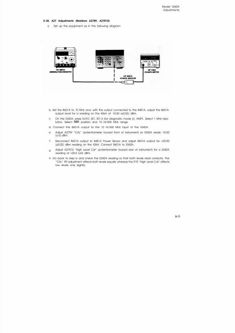
8/21/2019 HP5432 Microwave Frequency Counter
http://slidepdf.com/reader/full/hp5432-microwave-frequency-counter 102/364
Model 5342AAdjustments
5-38. A27 Adjustments (Resistors A27R9, A27R10)
a. Set up the equipment as in the following diagram:
b. Set the 8601A to 10 MHz and, with the output connected to the 8481A, adjust the 8601Aoutput level for a reading on the 436A of -10.00 (±0.02) dBm.
c. On the 5342A, press AUTO, SET, SET 6 (for diagnostic mode 6), AMPL. Select 1 MHz reso-lution. Select 50f2 position and 10 Hz-500 MHz range.
d. Connect the 8601A output to the 10 Hz-500 MHz input of the 5342A.
e. Adjust A27R9 “CAL” (potentiometer toward front of instrument) so 5342A reads -10.00
(±-0) dBm.
f. Reconnect 8601A output to 8481A Power Sensor and adjust 8601A output for +20.00(±0.02) dBm reading on the 436A. Connect 8601A to 5342A.
g. Adjust A27R10 “High Level Cal” (potentiometer toward rear of instrument) for a 5342Areading of +20.0 (±0) dBm.
h. Go back to step b and check the 5342A reading so that both levels read correctly. The“CAL” R9 adjustment affects both levels equally whereas the R10 “High Level Cal” affectslow levels only slightly.
5-11

8/21/2019 HP5432 Microwave Frequency Counter
http://slidepdf.com/reader/full/hp5432-microwave-frequency-counter 103/364
Model 5342AAdjustments
5-39. OPTION 002/003 ADJUSTMENTS
5-40. All, A25 Adjustments (Resistors A11R14, A25R31)
a. Set the equipment as in the following diagram:
b.
c.
d.
e.
f.
g.
h.
i.
j.
k.
Set signal source to 1000 (±5) MHz at a level of +8 (±0.5) dBm as measured on 436A PowerMeter.
Rotate A11R14, “DET”, fully ccw and A25R31, “OFFSET”, fully CW .
Set the 5342A to the 500 MHz-18 GHz range and AMPL mode,
Connect a scope probe (or dc voltmeter) to the “ATT” test point on A16.
Connect signal source to the 5342A RF input. Observe that the “ATT” test point goesto approximately 6.5 (± 1.5)V dc. If not, switch RF signal off and back on.
Adjust A25R31 slowly ccw just until “ATT” test point drops to approximately 1 (±1)V dc.
Rotate A11R14 fully CW .
Adjust signal source amplitude to -2 (±0.5) dBm and reconnect to 5342A RF input. “ATT”test point on A16 should remain at approximately 1 (±1)V dc.
Adjust A11R14 slowly ccw just until “ATT” test point on A16 jumps to approximately6.5 (±1.5)V dc.
If necessary, repeat adjustment procedures.
5-12

8/21/2019 HP5432 Microwave Frequency Counter
http://slidepdf.com/reader/full/hp5432-microwave-frequency-counter 104/364
Model 5342AAdjustments
5-41. OPTION 004 DIGITAL-TO-ANALOG (DAC) ADJUSTMENTS
5-42. Set up the equipment as shown below, and proceed:
a. Set the 5342A to the 500 MHz-18 GHz range, AUTO mode.
b. Connect DVM to DAC OUT, set DVM to 20V range.
c. Set the generator to 999 MHz as indicated on 5342A display.
d. On 5342A keyboard, press:
NOTE
The DAC variable resistor adjustments “OFFSET”(R27) and “GAIN ADJ” (R25) are located at the toprear of the A2 Display Driver Assembly. Remove thetop cover of the 5342A to gain access to these adjust-ments located below the top of the front frame.
e. Adjust “GAIN ADJ” and observe
f. On 5342A keyboard, press:
DVM for indication of 9.99 volts, dc.
g. Adjust “OFFSET” and observe DVM for 0 volts, dc.
h. Repeat steps d and f and observe DVM for proper indication. Readjust, if necessary.
5-13

8/21/2019 HP5432 Microwave Frequency Counter
http://slidepdf.com/reader/full/hp5432-microwave-frequency-counter 105/364
Model 5342AReplaceable Parts
SECTION VIREPLACEABLE PARTS
6-1. INTRODUCTION
6-2. This section contains information for ordering parts. Table 6-1 is a list of exchange assem-blies, and Table 6-2 lists abbreviations and reference designations used in the parts list andthroughout the manual. Table 6-3 lists all replaceable parts for the standard 5342A in referencedesignator order. Tables 6-4 ,6-5 ,6-6,6-7, and 6-8 list replaceable parts for Options 001,002,003,004, and 011, respectively. Table 6-9 contains the names and addresses that correspond to themanufacturer’s code numbers.
6-3. EXCHANGE ASSEMBLIES
6-4. Table 6-1 lists assemblies within the instrument that may be replaced on an exchange basis.Exchange factory repaired and tested assemblies are available only on a trade-in basis; therefore,the defective assemblies must be returned for credit. For this reason. assemblies required forspare parts stock must be ordered by the new assembly part number.
Table 6-1. Exchange Assemblies
NAME NEWHP PART NO. EXCHANGE HP PART NO.
U1 Sampler 5088-7022 5088-7522
Option 001 Oven Oscillator 10544-60011 10544-60511
Option 002 U2 Multiplexer/ 05342-80005 05342-80505A16U3 PROM — Matched (consists of matched 5088-7035 (consists of matched 5088-7535
and A16U3 PROM) and A16U3 PROM)
Option 002 U2 Multiplexer 5088-7035 5088-7535(must be ordered as matchedpart 05342-80505)
Option 003 U2 Attenuator 5088-7038 5088-7538
6-5. ABBREVIATIONS AND REFERENCE DESIGNATIONS
6-6. Table 6-2 lists abbreviations and reference designations used in the parts list, the schematicsand throughout the manual. In some cases, two forms of the abbreviation are used, one all incapital letters, and one partial or no capitals. This occurs because the abbreviations in the parts listare always all capitals. However, in the schematics and other parts of the manual, other abbrevi-ation forms are used with both lower case and upper case letters.
6-1
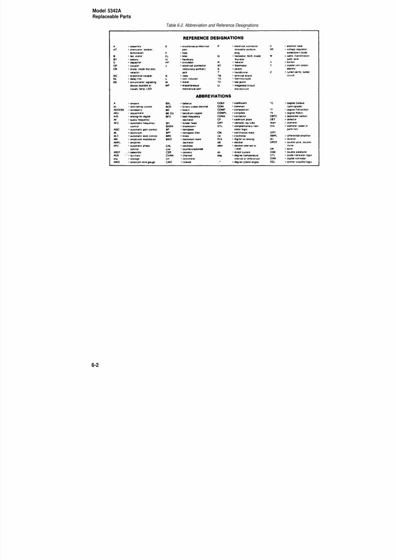
8/21/2019 HP5432 Microwave Frequency Counter
http://slidepdf.com/reader/full/hp5432-microwave-frequency-counter 106/364
Model 5342AReplaceable Parts
Table 6-2. Abbreviation and Reference Designations
6-2

8/21/2019 HP5432 Microwave Frequency Counter
http://slidepdf.com/reader/full/hp5432-microwave-frequency-counter 107/364
Model 5342AReplaceable Parts
Table 6-2. Abbreviations and Reference Designations (Continued)
6-3

8/21/2019 HP5432 Microwave Frequency Counter
http://slidepdf.com/reader/full/hp5432-microwave-frequency-counter 108/364
Model 5342AReplaceable Parts
6-7. REPLACEABLE PARTS LIST
6-8. Tab les 6-3 through 6-8 are the lists of replaceable parts and are organized as follows:
a, Electrical assemblies and their components in alphanumerical order by referencedesignation.
b. Chassis-mounted parts in alphanumerical order by reference designation (Table 6-3
only).c. Miscellaneous parts,
6-9, The information given for each part consists of the following:
a. The Hewlett-Packard part number.
b. Part number check digit (CD),
c. The total quantity (Qty) in each assembly.
d. The description of the part.
e. A typical manufacturer of the part in a five-digit code.
f. The manufacturer’s number for the part.
6-10. The total quantity for each assembly is given only once - at the first appearance of thepart number in the list for that assembly (A1, A2, etc.).
6-11. ORDERING INFORMATION * NOTE : P a r t s s u p p l i e r suse the fol lowing order ing data unt i l a parts manual . i s avai lable.6-12. 10 order a part listed in the replaceable parts table, quote the Hewlett-Packard partnumber, the check digit, indicate the quantity required, and address the order to the nearestHewlett-Packard office. The check digit will ensure accurate and timely processing of your order.
6-13. To order a part that is not listed in the replaceable parts table, include the instrumentmodel number, instrument serial number, the description and function of the part, and thenumber of parts required. Address the order to the nearest Hewlett-Packard Office.
6-14. DIRECT MAIL ORDER SYSTEM
6-15. Within the USA, Hewlett-Packard can supply parts through a direct mail order system.Advantages of using the system are as follows:
a. Direct ordering and shipment from the HP Parts Center in Mountain View, California.
b. No maximum or minimum on any mail order (there is a minimum order amount for partsordered through a local HP office when the orders require billing and invoicing).
c. Prepaid transportation (there is a small handling charge for each order).
d. No invo ices — to provide these advantages, a check or money order must accompanyeach order.
6-16. Mail order forms and specific ordering information is available through your HP office.Addresses and phone numbers are located at the back of this manual.
6-17. OPTION RETROFIT KITS
6-18. To order a retrofit kit for field installation of Options 001, 002, 003, 004, or 011paragraph 2-25 for the part number of the option kit,
*A re a c a l i b ra t i on and re p a i r c e nt e r s , d i re c t and ge ne ra l . s up p or t
a r e t o m a k e r e q u s t s f o r p a r t s t h r o u g h t h e l o c a l s u p p l y m i s s i o n .the raplaceable parts havet h rough t he s up p l y s y s t e m .
refer to
s hop sMany of
nat iona l s tock numbers and are ava i lab leA complete parts manual i s being prepared.
6-4

8/21/2019 HP5432 Microwave Frequency Counter
http://slidepdf.com/reader/full/hp5432-microwave-frequency-counter 109/364

8/21/2019 HP5432 Microwave Frequency Counter
http://slidepdf.com/reader/full/hp5432-microwave-frequency-counter 110/364

8/21/2019 HP5432 Microwave Frequency Counter
http://slidepdf.com/reader/full/hp5432-microwave-frequency-counter 111/364

8/21/2019 HP5432 Microwave Frequency Counter
http://slidepdf.com/reader/full/hp5432-microwave-frequency-counter 112/364

8/21/2019 HP5432 Microwave Frequency Counter
http://slidepdf.com/reader/full/hp5432-microwave-frequency-counter 113/364

8/21/2019 HP5432 Microwave Frequency Counter
http://slidepdf.com/reader/full/hp5432-microwave-frequency-counter 114/364
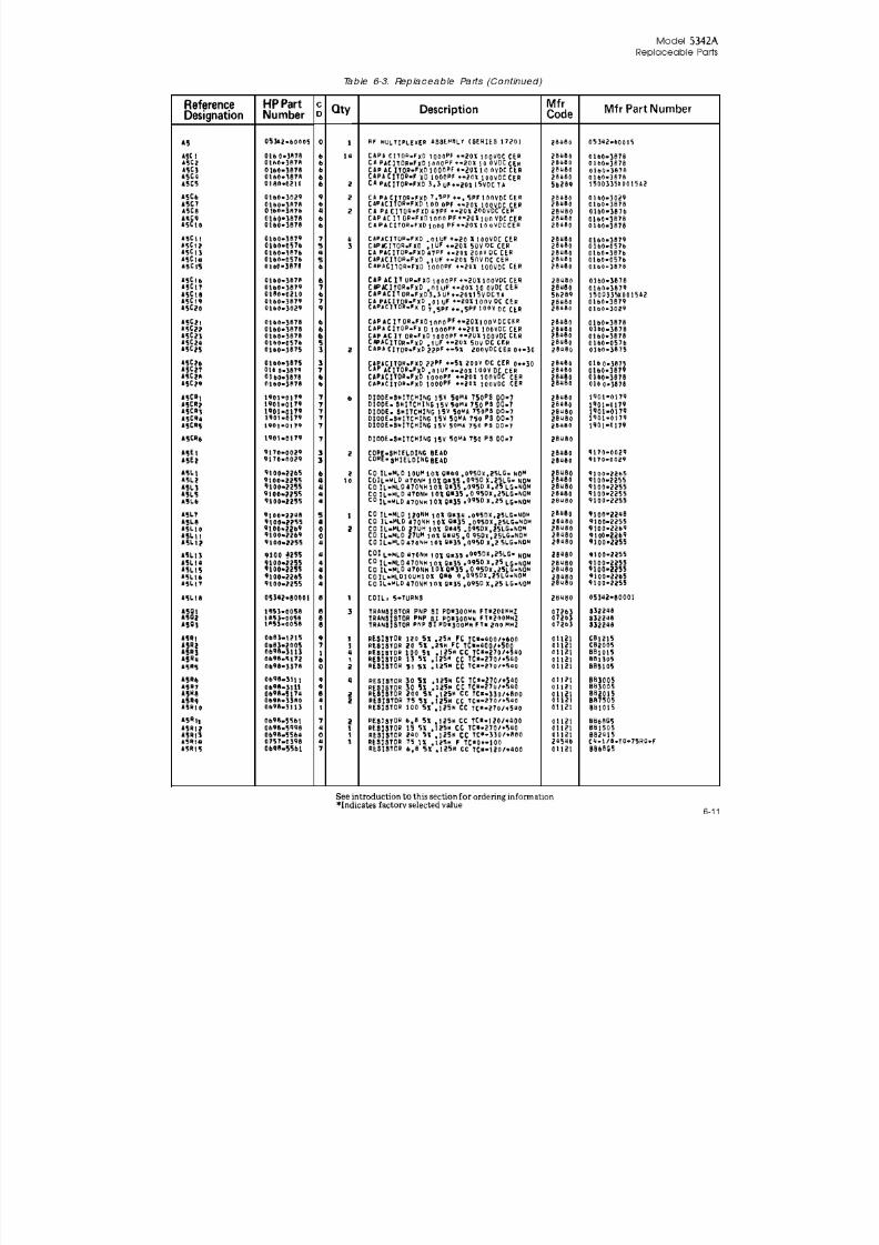
8/21/2019 HP5432 Microwave Frequency Counter
http://slidepdf.com/reader/full/hp5432-microwave-frequency-counter 115/364

8/21/2019 HP5432 Microwave Frequency Counter
http://slidepdf.com/reader/full/hp5432-microwave-frequency-counter 116/364

8/21/2019 HP5432 Microwave Frequency Counter
http://slidepdf.com/reader/full/hp5432-microwave-frequency-counter 117/364
Model 5342A
Replaceable PartsTable 6-3. Replaceable Parts (Continued)
Reference HP Part C Qty Description Mfr Mfr Part Number Designation Number D Code A6 05342-60006 1 1 OFFSET LOOP AMPLIFIER ASSEMBLY 28480 05342-60006
(SERIES 1720)
A6C1 0180-0228 6 2 CAPACITOR-FXD 22UF +-10% 15VDC TA 56289 1500226X9015B2 A6C2 0160-3879 7 6 CAPACITOR-FXD .01UF +-20% 100 VDC CER 28480 0160-3879
A6C3 0180-0210 6 2 CAPACITOR-FXD 3.3UF +-20% 15VDCTA 56289 150D335X0015A2 A6C4 0160-3879 7 CAPACITOR-FXD .01UF +-20% 100VDC CER 28480 0160-3879 A6C5 0160-3879 7 CAPACITOR-FXD .01UF +-20% 100VDC CER 28480 0160-3879 A6C6 0180-0210 6 CAPACITOR-FXD 3.3UF +-20% 15VDC TA 56289 150D335X0015A2 A6C7 0160-3879 7 CAPACITOR-FXD .01UF +-20% 100VDC CER 28480 0160-3879 A6C8 0180-0228 6 CAPACITOR-FXD 22UF +-10% 15VDC TA 56289 150D226X901582 A6C9 0180-1701 2 1 CAPACITOR-FXD 6,8UF +-20% 6VDC TA 56289 1500685X0006A2 A6C10 0160-0125 3 1 CAPACITOR-FXD 2.2UF +-20% 50VDC CER 28480 0160-0128 A6C11 0160-3879 7 CAPACITOR-FXD .01UF +-20% 100VDC CER 28480 0160-3879 A6C12 0160-0162 5 1 CAPACITOR-FXD .022UF +-10% 200VDC POLYE 28480 0160-0162 A6C13 0160-3879 7 CAPACITOR-FXD .01UF +-20% 100VDC CER 28480 0160-3879
A6CR1 1902-3193 3 2 DIODE-ZNR 13.3V 5% D0-7 PD=. 4W TC=+.059% 28480 1902-3193 A6CR2 1902-3193 3 DIODE-ZNR 13.3V 5% D0-7 PD=. 4W TC=+.059% 28480 1902-3193 A6CR3 1901-0040 1 2 DIODE-SWITCHING 30V 50MA 2NS DO=35 28480 1901-0040 A6CR4 1901-0040 1 DIODE-SWITCHING 30V 50MA 2NS DO=35 28480 1901-0040
A6Q1 1853-0020 4 3 TRANSISTOR PNP SI PD=300MW FT=150MHZ 28480 1853-0020 A6Q2 1854-0071 7 1 TRANSISTOR NPN SI PD=300MW FT=200MHZ 28480 1854-0071 A6Q3 1854-0020 4 TRANSISTOR PNP SI PD=300MW FT=150MHZ 28480 1853-0020 A6Q4 1853-0020 4 TRANSISTOR PNP SI PD=300MW FT=150MHZ 28480 1853-0020
A6R1 2100-2489 9 1 RESISTOR-TRMR 5K 10% C SIDE-ADJ 1=TRN 30983 ET50X502 A6R2 2100-2633 5 1 RESISTOR-TRMR 1K 10% C SIDE-ADJ 1=TRN 30983 ET50X102 A6R3 0757-0288 1 1 RESISTOR 9.90K 1% .125W F TC=0+-100 19701 MF4C1/8-T0-9091-F A6R4 0757-0279 0 4 RESISTOR 3.16K 1% .125W F TC=0+-100 24546 C4-1/8-T0-3161-F A6R5 0757-0442 9 2 RESISTOR 10K 1% .125W F TC=0+-100 24546 C4-1/8-T0-1002-F A6R6 0757-0280 3 4 RESISTOR 1K 1% .125W F TC=0+-100 24546 C4-1/8-T0-1001-F A6R7 0757-0442 9 RESISTOR 10K 1% .125 F TC=0+-100 24546 C4-1/8-T0-1002-F A6R8 0757-0279 0 RESISTOR 3.16K 1% .125W F TC=0+-100 24546 C4-1/8-T0-3161-F A6R9 0757-0280 3 RESISTOR 1K 1% .125W F TC=0+-100 24546 C4-1/8-T0-1001-F A6R10 0757-0416 7 1 RESISTOR 511 1% .125W F TC=0+-100 24546 C4-1/8-T0-511R-F A6R11 0757-0280 3 RESISTOR 1K 1% .125W F TC=0+-100 24546 C4-1/8-T0-1001-F A6R12 0757-0440 7 1 RESISTOR 7.5K 1% .125W F TC=0+-100 24546 C4-1/8-T0-7501-F A6R13 0757-0289 2 1 RESISTOR 13.3K 1% .125K F TC=0+-100 19701 MF4C1/8-T0-1332-F A6R14 0757-0280 3 RESISOTR 1K 1% .125W F TC=0+-100 24546 C4-1/8-T0-1001-F A6R15 0757-0279 0 RESISOTR 3.16K 1% .125W F TC=0+-100 24546 C4-1/8-T0-3161-F A6R16 0757-0438 3 1 RESISTOR 5.11K 1% .125 F TC=0+-100 24546 C4-1/8-T0-T111-F A6R17 0757-0200 7 1 RESISTOR 5.62K 1% .125W F TC=0+-100 24546 C4-1/8-T0-5621-F A6R18 0757-0424 7 1 RESISTOR 1.1K 1% .125W F TC=0+-100 24546 C4-1/8T0-1101-F A6R19 0757-0407 6 1 RESISTOR 200 1% .125W F TC=0+-100 24546 C4-1/8-T0-201-F A6R20 0757-0401 0 1 RESISTOR 100 1% .125 F TC=+-100 24546 C4-1/8-T0-101-F A6R21 0698-3153 9 1 RESISTOR 3.83K 1% .125 F TC=0+-100 24546 C4-1/8-T0-3831-F A6R22 0757-0199 3 1 RESISTOR 21.5K 1% .125 F TC=0+-100 24546 C4-1/8-T0-2152-F A6R23 0757-0427 0 2 RESISTOR 1.5K 1% .125W F TC=0+-100 24546 C4-1/8-T0-1501-F A6R24 0757-0427 0 RESISTOR 1.5K 1%.125W F 5C=0+-100 24546 C4-1/8-T0-1501-F A6R25 0757-0279 0 RESISTOR 3.16K 1% .125W F TC=0+-100 24546 C4-1/8-T0-3161-F A6U1 1820-1425 6 1 IC SCHMITT-TRIG TYL LS NAND QUAD 2-INP 01295 5N74LS132N A6U2 1820-0493 6 1 IC OP AMP 8-DIP-P 27014 LM307H
A6 MISCELLANEOUS PARTS
1251-0600 0 1 CONNECTOR-SGL CONT PIN 1.14-MM-88C-8Z SQ 28480 1251-06005000-9043 6 1 PIN:P.C. BOARD EXTRACTOR 28480 5000-90435040-6852 3 1 EXTRACTOR, ORANGE 28480 5040-6852
See introduction to this section for ordering, information*Indicates factory selected value
6-13

8/21/2019 HP5432 Microwave Frequency Counter
http://slidepdf.com/reader/full/hp5432-microwave-frequency-counter 118/364
Model 5342AReplaceable Parts
Table 6-3. Replaceable Parts (Continued)Reference HP Part C Qty Description Mfr Mfr Part Number Designation Number D Code A7 05342-60007 2 1 MIXER/SEARCH CONTROL ASSEMBLY 28480 05342-60007
(SERIES 1720) A7C1 0160-3879 7 9 CAPACITOR-FXD .01UF +-20% 100VDC CER 28480 0160-3879 A7C2 0160-3879 7 CAPACITOR-FXD .01UF +-20% 100VDC CER 28480 0160-3879 A7C3 0180-0155 8 2 CAPACITOR-FXD 2.2UF +-20% 20VDC TA 56289 150D225X0020A2
A7C4 0160-3879 7 CAPACITOR-FXD .01UF +-20% 100VDC CER 28480 0160-3879 A7C5 0180-0155 8 CAPACITOR-FXD 2.2UF +-20% 20VDC TA 56289 1S0D225X0020A2 A7C6 0160-3878 6 10 CAPACITOR-FXD 100PF +-20% 100VDC CER 28480 0160-3878 A7C7 0180-1701 2 4 CAPACITOR-FXD 6.8UF +-20% 6VDC TA 56289 150D685X0006A2 A7C8 0160-3879 7 CAPACITOR-FXD .01UF +-20% 100VDC CER 28480 0160-3879 A7C9 0180-1701 2 CAPACITOR-FXD 6,8UF +-20% 6VDC TA 56289 150D685X0006A2 A7C10 0160-3878 6 CAPACITOR-FXD 1000PF +-20% 100VDC CER 28480 0160-3878 A7C11 1080-1701 2 CAPACITOR-FXD 6.8UF +-20% 6VDC TA 56289 15D0685X0006A2 A7C12 0160-3878 6 CAPACITOR-FXD 1000PF +-20% 100VDC CER 28480 0160-3878 A7C13 0160-2879 7 CAPACITOR-FXD .01UF +-20% 100VDC CER 28480 0160-3879 A7C14 0180-1701 2 CAPACITOR-FXD 6.8UF +-20% 6VDC TA 56289 150D685X0006A2 A7C15 0160-3875 7 CAPACITOR-FXD .01UF +-20% 100VDC CER 28480 0160-3879 A7C16 0160-3875 3 1 CAPACITOR-FXD 22PF +-5% 200VDC CER 0+-30 28480 0160-3875 A7C17 1060-3878 6 CAPACITOR-FXD 1000PF +-20% 100VDC CER 28480 0160-3878 A7C18 1060-3878 6 CAPACITOR-FXD 1000PF +-20% 100VDC CER 28480 0160-3878 A7C19 0160-3879 7 CAPACITOR-FXD .01UF +-20% 100VDC CER 28480 0160-3879 A7C20 0160-3877 5 2 CAPACITOR-FXD 100PF +-20% 200VDC CER 28480 0160-3877 A7C21 0160-3878 6 CAPACITOR-FXD 1000PF +-20% 100VDC CER 28480 0160-3878 A7C22 0160-3879 7 CAPACITOR-FXD .01UF +-20% 100VDC CER 28480 0160-3879 A7C23 0160-3878 6 CAPACITOR-FXD 1000PF +-20% 100VDC CER 28480 0160-3878 A6C24 0160-3878 6 CAPACITOR-FXD 1000PF +-20% 100VDC CER 28480 0160-3878 A7C25 0160-3879 7 CAPACITOR-FXD .01UF +-20% 100VDC CER 28480 0160-3879 A7C26 0160-3878 6 CAPACITOR-FXD 1000PF +-20% 100VDC CER 28480 0160-3878 A7C27 0160-3877 5 CAPACITOR-FXD 100PF +-20% 200VDC CER 28480 0160-3877 A7C28 0160-3878 6 CAPACITOR-FXD 1000PF +-20% 100VDC CER 28480 0160-3878 A7CR1 1901-0518 8 2 DIODE-SCHOTTKY 28480 1901-0518 A7CR2 1901-0518 8 DIODE SCHOTTKY 28480 1901-0518 A7L1 9100-2268 9 8 COIL-MLD 22UH 10% Q=45 .095DX.25LG-NOM 28480 9100-2268 A7L2 9100-2268 9 COIL-MLD 22UH 10% Q=45 .095DX.25LG-NOM 28480 9100-2268 A7L3 9100-2247 4 3 COIL-MLD 100NH 10% Q=34 .095DX.25LG-NOM 28480 9100-2247 A7L4 9100-2268 9 COIL-MLD 22UH 10% Q-45 .095DX.25LG-NOM 28480 9100-2268 A7L5 9100-2268 9 COIL-MLD 10% Q=45 .095DC.25LG-NOM 28480 9100-2268 A7L6 9100-2247 4 COIL-MLD 100 NH 10% Q=34 .095DX.25LG-NOM 28480 9100-2247 A7L7 9100-2268 9 COIL-MLD 22UH 10% Q=45 .095DX.25LG-NOM 28480 9100-2268 A7L8 9100-2268 9 COIL-MLD 22UH 10% Q=45 .095DX.25LG-NOM 28480 9100-2268 A7L9 9100-2247 4 COIL-MLD 100 NH 10% Q=34 .095DX.25LG-NOM 28480 9100-2247 A7L10 9100-2268 9 COIL-MLD 22UH 10% Q=45 .095DX.25LG-NOM 28480 9100-2268 A7L11 9100-2268 9 COIL-MLD 22UH 10% Q=45 .095DX.25LG-NOM 28480 9100-2268 A7Q1 1854-0345 8 2 TRANSISTOR NPN 2N5179 SI TO-72 PD=200MA 04713 2N5179 A7Q2 1854-0092 2 2 TRANSISTOR NPN SI PD*200MW FT=600MHZ 28480 1854-0092 A7Q3 1854-0092 2 TRANSISTOR NPN SI PD*200MW FT=600MHZ 28480 1854-0092 A7Q4 1854-0071 7 2 TRANSISTOR NPN SI PD*300MW FT=200MHZ 28480 1854-0071 A7Q5 1854-0071 7 TRANSISTOR NPN SI PF*300MW FT=200MHZ 28480 1854-0071 A7Q6 1854-0345 8 TRANSISTOR NPN 2N5179 SI T0-72 PD=200MW 04713 2N5179 A7R1 0698-7101 5 1 RESISTOR 3K 5% .125W cc TC=-350/+857 01121 BB3025 A7R2 0698-5426 3 2 RESISTOR 10K 10% .125W CC TC=-350/+857 01121 BB1031 A7R3 0698-5426 3 RESISTOR 10K 10% .125W CC TC=-350/+857 01121 BB1031 A7R4 0698-5180 6 4 RESISTOR 2K 5% .125W CC TC=-350/+857 01121 BB2025 A7R5 0698-5181 7 1 RESISTOR 3.6K 5% .125W CC TC=-350/+857 01121 BB3625 A7R6 0698-6294 5 1 RESISTOR 47K 5% .125W CC TC=-466/+875 01121 BB4735 A7R7 0698-3378 0 2 RESISTOR 51 5% .125W CC TC=-270/+540 01121 BB5105 A7R8 0698-5075 8 2 RESISTOR 130 5% .125W CC TC=-330/+800 01121 BB1315 A7R9 0698-3113 1 3 RESISTOR 100 5% .125W CC TC=-270/+540 01121 BB1015 A7R10 0698-5172 6 2 RESISTOR 13 5% .125W CC TC=-270/+540 01121 BB1305 A7R11 0698-5567 3 1 RESISTOR 27K 5% .125W CC TC=-466/+875 01121 BB2735 A7R12 0698-5174 8 1 RESISTOR 200 5% .125 CC TC=-330/+800 01121 BB2015 A7R13 0698-3113 1 RESISTOR 100 5% .125W CC TC=-270/+540 01121 BB1015 A7R14 0698-5565 1 1 RESISTOR 2.2K 5% .125W CC TC=-350/+857 01121 BB2225 A7R15 0698-5180 6 RESISTOR 2K 5% .125 CC TC=-350/+857 01121 BB2025 A7R16 0698-5180 6 RESISTOR 2K 5% .125 CC TC=-350/+857 01121 BB2025 A7R17 0698-5180 6 RESISTOR 2K 5% .125W CC TC=-350/+857 01121 BB2025 A7R18 0698-3378 0 RESISTOR 51 5% .125W CC TC=-270/+540 01121 BB5105 A7R19 0698-5075 8 RESISTOR 130 5% .125W CC TC=-330/+800 01121 BB1315 A7R20 0698-5172 6 RESISTOR 13 5% .125W CC TC=-270/+540 01121 BB1305 A7R21 0698-3113 1 RESISTOR 100 5% .125W CC TC=-270/+540 01121 BB1015 A7R22 0698-3379 1 1 RESISTOR 68 5% .125W CC TC=-270/+540 01121 BB8805 A7TP1 1251-0600 0 1 CONNECTOR SGL CONT PIN 1.14-MM-BSC-SZ SQ 28480 1251-0600 A7U1 1820-0630 3 1 IC MISC TTL 04713 MC4044P A7U2 1820-1208 1 1 IC GATE TTL LS NOR TPL 3-INP 01295 SN74LS27N A7U3 1826-0372 2 2 IC 5 GHZ LIMITER/AMP 28480 1826-0732 A7U4 1826-0372 2 IC 5 GHZ LIMITER/AMP 28480 1826-0372
See introduction to this section for ordering, information*Indicates factory selected value
6-14

8/21/2019 HP5432 Microwave Frequency Counter
http://slidepdf.com/reader/full/hp5432-microwave-frequency-counter 119/364
Model 5342AReplaceable Parts
Table 6-3. Replaceable Parts (Continued)Reference HP Part C Qty Description Mfr Mfr Part Number Designation Number D Code
AB 05342-60008 1 1 MAIN VCD ASSEMBLY (SERIES IT26) 28480 05842-60806 ABC1 0160-0228 6 1 CAPACITOR-FXD 22LF**104 15960 TA 56289 1805224X441582 ABC2 0160-3878 6 14 CAPACITOR-FXD 1006PF +-20% 100VDC CER 28480 0160-3878 ABC3 0160-3878 6 CAPACITOR-FXD 1000PF +-20% 100VDC CER 28480 0160-3878 ABC4 0160-3877 5 4 CAPACITOR-FXD 1000PF +-20% 200VDC CER 28480 0160-3878
ABC5 0160-3878 6 CAPACITOR-FXD 1000PF +-20% 100VDC CER 28480 0160-3878 ABC6 0160-3877 5 1 CAPACITOR-FXD 1000PF +-20% 200VDC CER 28480 0160-3877 ABC7 0160-3877 0 CAPACITOR-FXD 2.28F +-.25RF 200VDC CER 28480 0160-3872 ABC8 0160-3878 6 CAPACITOR-FXD 1000PF +-20% 100VDC CER 28480 0160-3878 ABC9 0160-3878 6 CAPACITOR-FXD 1000PF +-20% 100VDC CER 28480 0160-3878 ABC10 0160-3878 6 CAPACITOR-FXD 1000PF +-20% 100VDC CER 28480 0160-3878 ABC11 0160-3878 6 CAPACITOR-FXD 1000PF +-20% 100VDC CER 28480 0160-3878 ABC12 0160-3877 5 CAPACITOR-FXD 1000PF +-20% 200VDC CER 28480 0160-3877 ABC13 0160-3878 6 CAPACITOR-FXD 1000PF +-20% 100VDC CER 28480 0160-3878 ABC14 0160-3878 6 CAPACITOR-FXD 1000PF +-20% 100VDC CER 28480 0160-3878 ABC15 0160-3878 6 CAPACITOR-FXD 1000PF +-20% 100VDC CER 28480 0160-3878 ABC16 0160-3878 6 CAPACITOR-FXD 1000PF +-20% 100VDC CER 28480 0160-3878 ABC17 0160-3877 5 CAPACITOR-FXD 100PF +-20% 200VDC CER 28480 0160-3877 ABC20 0160-3878 6 CAPACITOR-FXD 1000PF +-20% 100VDC CER 28480 0160-3878 ABC21 0160-3878 6 CAPACITOR-FXD 1000PF +-20% 100VDC CER 28480 0160-3878 ABC22 0160-3878 6 CAPACITOR-FXD 1000PF +-20% 100VDC CER 28480 0160-3878 ABC23 0180-0210 6 CAPACITOR-FXD 1000PF +-20% 100VDC CER 28480 0160-3878 ABC24 0180-1701 6 1 CAPACITOR-FXD 3.30F +-20% 15VDC TA 56289 1500335X001542 ABC25 0180-1701 2 0 CAPACITOR-FXD 6.80F +-20% 6VDC TA 56289 1500685X000642
ABC26 0180-3075 2 CAPACITOR-FXD 6.80F +-20% 6VDC TA 28480 1500685X000642 ABC27 0180-1701 6 CAPACITOR-FXD 1000PF +-20% 100VDC CER 56289 0160-3878 ABC28 0180-1701 2 CAPACITOR-FXD 6.80F +-20% 6VDC TA 56289 1500685X000642 ABC29 0180-3876 2 CAPACITOR-FXD 6.80F +-20% 6VDC TA 28480 1500685X000642 ABC41 0122-4069 6 CAPACITOR-FXD 1000PF +-20% 100VDC CER 28480 0160-3878 ABC42 0122-0065 7 2 CAPACITOR: VOLTAGE VAR:29 PF/3V 28480 0122-0065 ABC43 1902-3179 7 CAPACITOR: VOLTAGE VAR:29 PF/3V 28480 0122-0065 ACL0 9120-0016 7 1 DIODE-2NR 5% 00.7 PDF, 48 TC49.0624 28480 1902-3171 ABL1 9100-2268 8 1 CORE, SHIELDING HEAD 28480 0170-0016 ABL2 9100-2268 9 4 COIL-MLD 22UH 10% Q*45 .095DX, 25LG. NOM 28480 9100-2268 ABL3 9100-2267 9 COIL-MLD 22UH 10% Q*45 .095DX, 25LG. NOM 28480 9100-2268 ABLU 9100.2268 9 3 COIL-MLD 100UH 10% Q*34 .095DX, 25LG. NOM 28480 9100-2247 ABL5 0100-2268 9 COIL-MLD 22UH 10% Q*45 .095DX, 25LG. NOM 28480 9100-2268 ABL6 9100-2268 9 COIL-MLD 22UH 10% Q*45 .095DX, 25LG. NOM 28480 9100-2268 ABL7 9100-2268 4 COIL-MLD 100UH 10% Q*34 .095DX, 25LG. NOM 28480 9100-2247 ABL8 9100-2268 9 COIL-MLD 22UH 10% Q*45 .095DX, 25LG. NOM 28480 9100-2265 ABL9 9100-2268 9 COIL-MLD 22UH 10% Q*45 .095DX, 25LG. NOM 28480 9100-2268 ABL10 9100-2268 9 COIL-MLD 22UH 10% Q*45 .095DX, 25LG. NOM 28480 9100-2268 ABL11 9100-2268 9 COIL-MLD 100UH 10% Q*34 .095DX, 25LG. NOM 28480 9100-2247
ABL12 9100-2268 9 COIL-MLD 22UH 10% Q*45 .095DX, 25LG. NOM 28480 9100-2268 ACSF 9100-2268 9 COIL-MLD 22UH 10% Q*45 .095DX, 25LG. NOM 28480 9100-2268 ACOF 9100-2268 8 1 TRANSISTOR NPN 2N5179 31 TO-72 PD=200HW 28480 2N5179 ADE1 0698-5174 7 1 TRANSISTOR NPN S1 PD=30007 FT-200MHZ 28480 1854-0071 ADE2 0698-3394 6 1 RESISTOR 200 5X .125M CC TC=-130/4600 01121 BB2015 ADE3 0698.5172 6 3 RESISTOR 43 5X .125M CC TC=-270/4540 01121 BB4303 ADE4 0698-5994 6 3 RESISTOR 13 5X .125M CC TC=-270/4540 01121 BB1305 ADE5 0698-3376 5 1 RESISTOR 560 5X .125M CC TC=-330/4800 01121 BB5615 ADE6 0698-5079 6 RESISTOR 43 5X .125M CC TC=-270/4540 01121 BB4305 ADE7 0698-3374 8 3 RESISTOR 130 5X .125M CC TC=-330/4800 01121 BB1315 ADE8 0698-3374 0 3 RESISTOR 51 5X .125M CC TC=-270/4540 01121 BB5105 ADE9 0698-3342 6 RESISTOR 43 5X .125M CC TC=-270/4800 01121 BB4305 ADE10 0698-5352 6 1 RESISTOR 120 5X .125M CC TC=-330/4800 01121 BB1215 ADE11 0698-5635 6 RESISTOR 13 5X .125M CC TC=-270/4540 01121 BB1305 ADE12 0698-3942 8 RESISTOR 130 5X .125M CC TC=-330/4800 01121 BB1315 ADE13 0698-3942 5 3 RESISTOR 4.71 5X .125M CC TC=-350/4857 01121 BB4725 ADE14 0698-3942 5 RESISTOR 4.71 5X .125M CC TC=-350/4857 01121 BB4725 ADE15 0698-3942 5 RESISTOR 4.71 5X .125M CC TC=-350/4857 01121 BB4725 ADE16 0698-5136 0 RESISTOR 31 5X .125M CC TC=-270/4540 01121 BB5105
ADE17 0698-2212 6 1 RESISTOR 100 05X .125M F TC=0+-100 24546 C3-1/8-TO-100R-G ADE18 0698-5132 6 RESISTOR 13 5X .125M CC TC=-270/4500 01121 BB1305 ADE19 0698-5615 6 RESISTOR 130 5X .125M CC TC=-330/4800 01121 BB1315 ADE20 0698-5385 6 1 RESISTOR 75 5X .125M CC TC=-275/4500 01121 BB7505 ADE21 0698-1576 6 RESISTOR 51 5X .125M CC TC=-RTC/4540 01121 BB5105 ADE22 0698-5426 6 5 RESISTOR 10 5X .125M CC TC=-350/4859 01121 BB1031 ADE23 2330-2489 1 RESISTOR 749 10X .125M C SIDEWADJ 1-TRW 30413 BB50X502 ADU1 0698-5936 2 1 RESISTOR 1.58 5X .125M CC TC=-350/4857 01121 BB1525
7820-3622 2 1 10 5 GHZ LIMITER/AMP 28480 1828-03720333-0133 2 AB MISCELLANEOUS PARTS
6 2 CONTACT-FINGER 13-WD DD-FREE-HGT BB-CU 28480 0383-01330330-0020 4 1 STANDARD 375-IN-LG 440THD 28480 0380-09700542-2010 3 1 SCREW, GROUND 28480 05342-20101
See introduction to this section for ordering information*Indicates factory selected value
6-15

8/21/2019 HP5432 Microwave Frequency Counter
http://slidepdf.com/reader/full/hp5432-microwave-frequency-counter 120/364
Model 5342AReplaceable Parts
Table 6-3. Replaceable Parts (Continued)
Reference HP Part C Qty Description Mfr Mfr Part Number Designation Number D Code A9 05342-60009 4 1 MAIN LOOP AMPLIFIER ASSEMBLY 28480 05342-60009
S(SERIES 1720)
A9C1 0160-4084 8 2 CAPACITOR-FXD .1UF +-20% 50VDC CER 28480 0160-4084 A9C2 0160-0165 8 1 CAPACITOR-FXD .056UF +-10% 200VDC POLYE 28480 0160-0165 A9C3 0180-0210 6 2 CAPACITOR-FXD 3.3UF +-20% 15VDC TA 56289 150D335X0015A2 A9C4 0160-3879 7 5 CAPACITOR-FXD.01UF +-20% 100VDC CER 28480 0160-3879 A9C5 0160-3879 7 CAPACITOR-FXD .01UF +-20% 100VDC CER 28480 0160-3879 A9C6 0180-1701 P 1 CAPACITOR-FXD 6.8UF +-20% 6VDC TA 56289 150D685X0006A2 A9C7 0160-3879 7 CAPACITOR-FXD .01UF +-20% 100VDC CER 28480 0160-3879 A9C8 0160-0301 4 1 CAPACITOR-FXD .012UF +-10% 200VDC POLYE 28480 0160-0301 A9C9 0160-0153 4 2 CAPACITOR-FXD 1000PF +-10% 200VDC POLYE 28480 0160-0153 A9C10 0160-0160 3D 1 CAPACITOR-FXD 8200PF +-10% 200VDC POLYE 28480 0160-0160 A9C11 0160-4084 8 CAPACITOR-FXD .1UF +-20% 50VDC CER 28480 0160-4084 A9C12 0140-0200 0 1 CAPACITOR-FXD 390PF +-5% 300VDC MICA 72136 DM15F391J0300WV1CR A9C13 0180-0228 6 2 CAPACITOR-FXD 22UF +-10% 15VDC TA 56289 150D226X901582 A9C14 0180-0210 6 CAPACITOR-FXD 3.3UF +-20% 15VDC TA 56289 150D335X001542 A9C15 0160-3879 7 CAPACITOR-FXD .01UF +-20% 100VDC CER 28480 0160-3879 A9C16 0160-0153 4 CAPACITOR-FXD 1000PF +-10% 200VDC POLYE 28480 0160-0153 A9C17 0180-0228 6 CAPACITOR-FXD 22UF +-10% 15VDC TA 56389 150D226X9015H2 A9C18 0160-0137 4 1 CAPACITOR-FXD .33UF +-20% 25VDC CER 28480 0160-0137 A9C19 0160-3879 7 CAPACITOR-FXD .01UF +-20% 100VDC CER 28480 0160-3879
A9CR1 1902-0049 2 2 DIODE-ZNR 6.19V 5% DO-7 PD.4W TC=+.022% 28480 1902-0049 A9CR2 1901-0040 1 2 DIODE-SWITCHING 30V 50MA 2NS DO-35 28480 1901-0040 A9CR3 1901-0040 1 DIODE-SWITCHING 30V 50MA 2NS DO-35 28480 1901-0040 A9CR4 1902-0049 2 DIODE-ZNR 6.19V 5% DO-7 PD=.4W TC*+-22% 28480 1902-0049
A9L1 9140-0131 5 3 COIL-MLD 10MM 5% Q=80 .24DX.74LG-NOM 28480 9140-0131 A9L2 9140-0131 5 COIL-MLD 10MM 5% Q=80 .24DX.74LG-NOM 28480 9140-0131 A9L3 9140-0131 5 COIL-MLD 10MM 5% Q=80 .24DX.74LG-NOM 28480 9140-0131
A9Q1 1853-0020 4 3 TRANSISTOR PNP SI PD=300MW FT=150MHZ 28480 1853-0020 A9Q2 1853-0020 4 TRANSISTOR PNP SI PD=300MW FT=150MHZ 28480 1853-0020 A9Q3 1853-0020 4 TRANSISTOR PNP SI PD=300MW FT=150MHZ 28480 1853-0020 A9Q4 1854-0071 7 1 TRANSISTOR PNP SI PD=300MW FT=200MHZ 28480 1854-0071
A9R1 0757-0279 0 2 RESISTOR 3.16K 1% .125W F TC=0+-100 24546 C4-1/8-T0-3161-F A9R2 0698-6123 9 2 RESISTOR 20K 5% .125W CC TC=-466/+875 01121 BB2035 A9R3 0757-0280 3 3 RESISTOR 1K 1% .125 F TC=0+-100 24546 C4-1/8-T0-1001-F A9R4 0757-0199 3 3 RESISTOR 21.5K 1% .125W F TC=0+-100 24546 C4-1/8-T0-2152-F
A9R5 0698-5184 0 2 RESISTOR 6.2K 5j% .125W CC TC=-350+857 01121 BB6225 A9R6 0757-0199 3 RESISTOR 21.5K 1% .125W F TC=0+-100 24546 C4-1/8-T0-2152-F A9R7 0698-6123 9 RESISTOR 20K 5% .125W CC TC=-466/+857 01121 BB2035 A9R8 0698-5184 0 RESISTOR 6.2K 5% .125W CC TC=-350/+857 01121 BB6225 A9R9 0698-3446 3 1 RESISTOR 383 1% .125W F TC=0+-100 24546 C4-1/8-T0-383R-F A9R10 0757-0279 0 RESISTOR 3.16K 1% .125W F TC=0+-100 24546 C4-1/8-T0-3161-F A9R11 0757-0280 3 RESISTOR 1K 1% .125W F TC=0+-100 24546 C4-1/8-T0-1001-F A9R12 0698-3150 6 1 RESISTOR 2.37K 1% .125W F TC=0+-100 24546 C4-1/8-T0-2371-F A9R13 0757-0290 5 1 RESISTOR 6.19K 1% .125W F TC=0+-100 19701 M4C1/8-T0-6191-F A9R14 0757-0198 3 RESISTOR 21.5K 1% .125W F TC=0+-100 24546 C4-1/8-T0-2152-F A9R15 0757-0418 9 1 RESISTOR 619 1% .125W F TC=0+-100 24546 C4-1/8-T0-619R-F A9R16* 0683-1065 7 1 RESISTOR 10M 5% .25W FC TC=-900/+1000 01121 C81065 A9R17 0757-0283 6 2 RESISTOR 2K 1% .125 F TC=0+-100 24546 C4-1/8-T0-2001-F A9R18 0757-0280 3 RESISTOR 1K 1% .125W F TC=0+-100 24546 C4-1/8-T0-1001-F A9R19 0757-0283 6 RESISTOR 2K 1% .125W F TC=0+-100 24546 C4-1/8-T0-2001-F
A9S1 1820-1325 5 1 IC SW CMDS BILATL QUAD 01928 CD4066AE
A9TP1 1251-0600 0 1 CONNECTOR-SGL CONT PIN 1.14-MM-BSC-S2 SQ 28480 1251-0600
A9U1 1820-1112 8 1 IC FF TTL LS D-TYPE POS-EDGE-TRIG 01295 SN74LS74N A9U2 1820-0493 6 1 IC OP AMP 8-DIP-P 27014 LM307N
A9 MISCELLANEOUS PARTS
5000-9043 6 1 PIN: P.C. BOARD EXTRACTOR 28480 5000-90435040-6852 3 1 EXTRACTOR, ORANGE 28480 5040-6852
See introduction to this section for ordering, information*Indicates factory selected value
6-16

8/21/2019 HP5432 Microwave Frequency Counter
http://slidepdf.com/reader/full/hp5432-microwave-frequency-counter 121/364
Model 5342AReplaceable Parts
Table 6-3. Replaceable Parts (Continued)
Reference HP Part C Qty Description Mfr Mfr Part Number Designation Number D Code
A10 05342-60010 7 1 DIVIDE-BY-N ASSEMBLY (SERIES 1720) 28480 05342-60010
A10C1 0180-1701 2 4 CAPACITOR-FXD 6.8UF +-20% 6VDC TA 56289 150D685X0006A2
A10C2 0180-0106 9 1 CAPACITOR-FXD 60UF +-20% 6VDC TA 56289 150D606X0006B2HA10C3D 0180-1701 2 CAPACITOR-FXD 6.8UF +-20% 6VDC TA 56289 150D685X0006A2 A10C4 0160-3878 6 15 CAPACITOR-FXD 1000PF +-20% 100VDC CER 28480 0160-3878 A10C5 0160-3878 6 CAPACITOR-FXD 1000PF +-20% 100VDC CER 28480 0160-3878 A10C6 0160-3878 6 CAPACITOR-FXD 1000PF +-20% 100VDC CER 28480 0160-3878 A10C7 0180-1701 2 CAPACITOR-FXD 6.8UF +-20% 6VDC TA 56289 150D685X0006A2 A10C8 0180-1701 2 CAPACITOR-FXD 6.8UF +-20% 6VDCTA 56289 150D685X0006A2 A10C9 0160-3878 6 CAPACITOR-FXD 1000PF +-20% 100VDC CER 28480 0160-3878 A10C10 0160-3878 6 CAPACITOR-FXD 1000PF +-20% 100VDC CER 28480 0160-3878 A10C11 0160-3875 3 1 CAPACITOR-FXD 22PF +-5% 200VDC CER 0+-30 28480 0160-3875 A10C12 0160-3878 6 CAPACITOR-FXD 1000PF +-20% 100VDC CER 28480 0160-3878 A10C13 0160-3878 6 CAPACITOR-FXD 1000PF +-20% 100VDC CER 28480 0160-3878 A10C14 0160-3878 6 CAPACITOR-FXD 1000PF +-20% 100VDC CER 28480 0160-3878 A10C15 0160-3878 6 CAPACITOR-FXD 1000PF +-20% 100VDC CER 28480 0160-3878 A10C16 0160-3878 6 CAPACITOR-FXD 1000PF +-20% 100VDC CER 28480 0160-3878 A10C17 0160-3878 6 CAPACITOR-FXD 1000PF +-20% 100VDC CER 28480 0160-3878 A10C18 0160-3878 6 CAPACITOR-FXD 1000PF +-20% 100VDC CER 28480 0160-3878 A10C19 0160-3878 6 CAPACITOR-FXD 1000PF +-20% 100VDC CER 28480 0160-3878 A10C20 0160-3878 6 CAPACITOR-FXD 1000PF +-20% 100VDC CER 28480 0160-3878
A10C21 0160-3878 6 CAPACITOR-FXD 1000PF +-20% 100VDC CER 28480 0160-3878
A10L1 9100-2268 9 1 COIL,MLD 22UH 10% Q=45 .095DX .25LG-NOM 28480 9100-2268 A10L2 9100-1788 6 3 CHOKE-WIDE BAND ZMAX=680 OHM@ 180 MHZ 2114 VK200 20/48 A10L3 9100-1788 6 CHOKE-WIDE BAND ZMAX=680 OHM@ 180 MHZ 2114 VK200 20/48 A10L4 9100-1788 6 CHOKE-WIDE BAND ZMAX=680 OHM@ 180 MHZ 2114 VK200 20/48
A10R1 0675-1021 8 2 RESISTOR 1K 10% .125W CC TC=-330/+800 01121 BB1021 A10R2 0698-5996 2 1 RESISTOR 560 5% .125W CC TC=-330/+800 01121 BB5615 A10R3 0698-8073 2 1 RESISTOR 1.6K 5% .125W CC TC=-350/+857 01121 BB1625 A10R4 0698-3114 2 1 RESISTOR 300 5% .125W CC TC=-330/+800 01121 BB3015 A10R5 0698-6242 3 1 RESISTOR 1.2K 5% .125W CC TC=-350/+857 01121 BB1225 A10R6 0698-3380 4 1 RESISTOR 75 5% .125W CC TC=-270/+540 01121 BB7505 A10R7 0698-5177 1 1 RESISTOR 820 5% .125 cc TC=-330/+800 01121 BB8215 A10R8 0698-7101 5 1 RESISTOR 3K 5% .125 CC TC=-350/+857 01121 BB3025 A10R9 0698-5565 1 1 RESISTOR 2.2K 5% .125W CC TC=-350/+857 01121 BB2225 A10R10 0698-3376 8 1 RESISTOR 43 5% .125W CC TC-270/+540 01121 BB4305 A10R11 0675-1021 8 RESISTOR 1K 10% .125W CC TC=-330/+800 01121 BB1021
A10TP1 1251-0600 0 1 CONNECTOR-SGL CONT PIN 1.14-MM-BSC-SZ SQ 28480 1251-0600
A10U1 1820-1251 6 1 IC CNTR TTL L8 DECD ASYNCHRO 01295 SN75LS196N A10U2 1820-0630 3 1 IC MISC TTL 04713 MC4044P A10U3 1820-0069 2 1 IC GATE TTL NAND DUAL 4-INP 01295 SN7420N A10U4 1820-1112 8 1 IC FF TTL LS D-TYPE POS-EDGE-TRIG 01295 SN74LS74N A10U5 1820-1225 4 1 IC FF ECL D-M/S DUAL 04713 MC10231P A10U6 1820-0736 0 1 IC CNTR ECL BIN DUAL 28480 1820-0736 A10U7 1820-0693 8 1 IC FF TTL S D-TYPE POS-EDGE-TRIG 01295 SN74S74N A10U8 1820-1429 0 4 IC CNTR TTL LS DECD SYNCHRO 01295 SN74LS160N A10U9 1820-1429 0 IC CNTR TTL LS DECD SYNCHRO 01295 SN74LS160N A10U10 1820-1196 8 3 IC FF TTL LS D-TYPE POS-EDGE-TRIG COM 01295 SN74LS174N A10U11 1820-1195 7 2 IC FF TTL LS D-TYPE POS-EDGE-TRIG COM 01295 SN74LS175N A10U12 1820-1888 5 1 IC PRESCR EDL 04713 MC12013L A10U13 1820-1429 0 IC CNTR TTL LS DECD SYNCHRO 01295 SN74LS160N A10U14 1820-1429 0 IC CNTR TTL LS DECD SYNCHRO 01295 SN74LS160N A10U15 1820-1196 8 IC FF TTL LS D-TYPE POS-EDGE-TRIG COM 01295 SN74LS174N A10U16 1820-1195 7 IC FF TTL LS D-TYPE POS-EDGE-TRIG COM 01295 SN74LS175N A10U17 1820-1196 8 IC FF TTL LS D-TYPE POS-EDGE-TRIG COM 01295 SN74LS174N
A10 MISCELLANEOUS PARTS
5000-9043 6 1 PIN: P.C. BOARD EXTRACTOR 28480 5000-90435040-6Y852 3 1 EXTRACTOR, ORANGE 28480 5040-6852
See introduction to this section for ordering, information*Indicates factory selected value
6-17

8/21/2019 HP5432 Microwave Frequency Counter
http://slidepdf.com/reader/full/hp5432-microwave-frequency-counter 122/364
Model 5342AReplaceable Parts
Table 6-3. Replaceable Parts (Continued)
Reference HP Part C Qty Description Mfr Mfr Part Number Designation Number D Code
A11 05442-60011 8 1 IF LIMITER ASSEMBLY (SERIES 1720) 28480 05342-60011
A11C1 0160-3879 7 5 CAPACITOR-FXD .01UF +-20% 100VDC CER 28480 0160-3879
A11C2 0160-3879 7 CAPACITOR-FXD .01UF +-20% 100VDC CER 28480 0160-3879 A11C3 0160-3879 7 CAPACITOR-FXD .01UF +-20% 100VDC CER 28480 0160-3879 A11C4 0160-3879 7 CAPACITOR-FXD .01UF +-20% 100VDC CER 28480 0160-3879 A11C5 0160-3879 7 CAPACITOR-FXD .01UF +-20% 100VDC CER 28480 0160-3879 A11C6 0180-0490 4 2 CAPACITOR-FXD 68UF +-10% 6VDC TA 90201 TDC686K006WLF A11C7 0180-0490 4 CAPACITOR-FXD 68UF +-10% 6VDC TA 90201 TDC686K006WLF
A11CR1 1901-0535 9 2 DIODE-SCHOTTKY 22840 1901-0535 A11CR2 1901-0535 9 DIODE-SCHOTTKY 22840 1901-0535
A11L1 9100-2247 4 1 COIL-MLD 100NH 10% Q=34 .095DX.25LG-NOM 28480 9100-2247 A11L2 9100-2265 6 2 COIL-MLD 10UH 10% Q=60 .095DX.25LG-NOM 28480 9100-2265 A11L3 9100-2265 6 COIL-MLD 10UH 10% Q=60 .095DX.25LG-NOM 28480 9100-2265
A11R1 2100-3207 1 1 RESISTOR-TRMR 5K 10% C SIDE-ADJ 1-TRN 28480 2100-3207 A11R2 0698-7102 6 1 RESISTOR 5.1K 5% .125W CC TC=-350/+857 01121 BB5125 A11R3 0698-5176 0 1 RESISTOR 510 5% .125W CC TC=-330/+800 01121 BB5115 A11R4 0698-7964 8 1 RESISTOR 100K 5% .125W CC TC=-466/+875 28480 0698-7964 A11R5 0698-3113 1 2 RESISTOR 100 5% .1125 CC TC=-270/+540 01121 BB1015
A11R6 0698-5996 2 1 RESISTOR 560 5% .125W CC TC=-330/+800 01121 BB5615 A11R7 0698-3111 9 1 RESISTOR 30 5% .125W CC TC=-270/+540 01121 BB3005 A11R8 0698-7185 5 2 RESISTOR 220K 5% .125W CC TC=-600/+1137 01121 BB2245 A11R9 0698-7185 5 RESISTOR 220K 5% .125W CC TC=-600/+1137 01121 BB2245 A11R10 0698-3113 1 RESISTOR 100 5% .125W CC TC=-270/+540 01121 BB1015 A11R11 0698-7026 3 1 RESISTOR 91 5% .125W CC TC=-270/+540 01121 BB9105 A11R12 0875-1021 8 1 RESISTOR 1K 10% .125W CC TC=-330/+800 01121 BB1021 A11R13 0698-5993 9 1 RESISTOR 8.2K 5% .125W CC TC=-350/+857 01121 BB8225 A11R14 2100-3352 7 1 RESISTOR-TRMR 1K 10% C SIDE-ADJ 1-TRN 28480 2100-3352
A11TP2 1251-0600 0 3 CONNECTOR-SGL CONT PIN 1.14-MM-BSC-SZ SQ 28480 1251-0600 A11TP3 1251-0600 0 CONNECTOR-SGL CONT PIN 1.14-MM-BSC-SZ SQ 28480 1251-0600 A11TP4 1251-0600 0 CONNECTOR-SGL CONT PIN 1.14-MM-BSC-SZ SQ 28480 1251-0600
A11U1 1826-0065 0 1 IC 311 COMPARATOR 8-DIP-P 01295 SN72311P A11U2 1826-0372 2 1 IC 5 GHZ LIMITER/AMP 28480 1826-0372
A11 MISCELLANEOUS PARTS
5000-9043 6 1 PIN: P.C. BOARD EXTRACTOR 28480 5000-90435040-6852 3 1 EXTRACTOR, ORANGE 28480 5040-6852
See introduction to this section for ordering, information*Indicates factory selected value
6-18

8/21/2019 HP5432 Microwave Frequency Counter
http://slidepdf.com/reader/full/hp5432-microwave-frequency-counter 123/364
Model 5342AReplaceable Parts
Table 6-3. Replaceable Parts (Continued)
Reference HP Part C Qty Description Mfr Mfr Part Number Designation Number D Code
A12 05342-60012 9 1 IF DETECTOR ASSEMBLY (SERIES 1720) 28480 05342-60012 A12C1 0160-3878 6 1 CAPACITOR-FXD 1000PF +-20% 100VDC CER 28480 0160-3878 A12C2 0160-3879 7 12 CAPACITOR-FXD .01UF +-20% 100VDC CER 28480 0160-3879
A12C3 0160-3879 7 CAPACITOR-FXD .01UF +-20% 100VDC CER 28480 0160-3879 A12C4 0160-3879 7 CAPACITOR-FXD .01UF +-20% 100VDC CER 28480 0160-3879 A12C5 0160-2262 0 2 CAPACITOR-FXD 16PF +-5% 500VDC CER 0+-30 28480 0160-2262 A12C6 0160-3877 5 1 CAPACITOR-FXD 100PF +-20% 200VDC CER 28480 0160-3877 A12C7 0160-2262 0 CAPACITOR-FXD 16PF +-5% 500VDC CER 0+-30 28480 0160-2262 A12C8 0160-3879 7 CAPACITOR-FXD .01UF +-20% 100VDC CER 28480 0160-3879 A12C9 0160-3879 7 CAPACITOR-FXD .01UF +-20% 100VDC CER 28480 0160-3879 A12C10 0150-0115 7 1 CAPACITOR-FXD 27PF +-10% 500VDC CER 28480 0150-0115 A12C11 0160-4084 8 1 CAPACITOR-FXD .1UF +-20% 50VDC CER 28480 0160-4084 A12C12 0180-0490 4 3 CAPACITOR-FXD 68UF +-10% 6VDC TA 90201 TDC686K006WLF A12C13 0160-3879 7 CAPACITOR-FXD .01UF +-20% 100VDC CER 28480 0160-3879 A12C14 0160-3879 7 CAPACITOR-FXD .01UF +-20% 100VDC CER 28480 0160-3879 A12C15 0160-3879 7 CAPACITOR-FXD .01UF+-20% 100VDC CER 28480 0160-3879 A12C16 0160-3879 7 CAPACITOR-FXD .01UF+-20% 100VDC CER 28480 0160-3879 A12C17 0160-3879 7 CAPACITOR-FXD .01UF+-20% 100VDC CER 28480 0160-3879 A12C18 0160-3879 7 CAPACITOR-FXD .01UF+-20% 100VDC CER 28480 0160-3879 A12C19 0160-3879 7 CAPACITOR-FXD .01UF+-20% 100VDC CER 28480 0160-3879 A12C20 0180-0491 5 2 CAPACITOR-FXD 10UF +-20% 25VDC TA 28480 0180-0491 A12C21 0180-0491 5 CAPACITOR-FXD 10UF +-20% 25VDC TA 28480 0180-0491
A12C22 0180-0490 4 CAPACITOR-FXD 68UF +-10% 6VDC TA 90201 5DC686K006WLF A12C23 0180-0490 4 CAPACITOR-FXD 68UF +-10% 6VDC TA 90201 5DC686K006WLF A12C24 0160-3872 0 1 CAPACITOR-FXD 2.2PF +-25PF 200VDC CER 28480 0160-3872 A12CR1 1901-0535 9 3 DIODE-SCHOTTKY 28480 1901-0535 A12CR2 1901-0535 9 DIODE-SCHOTTKY 28480 1901-0535 A12CR3 1901-0535 9 DIODE-SCHOTTKY 28480 1901-0535 A12CR4 1901-0040 1 12 DIODE-SWITCHING 30V 50MA 2NS DO-35 28480 1901-0040 A12L1 9100-2250 9 2 COIL-MLD 180NH 10% Q=34 .095DX.25LG-NOM 28480 9100-2250 A12L2 9100-2250 9 COIL-MLD 180NH 10% Q=34 .095DX.25LG-NOM 28480 9100-2250 A12L3 9100-2250 6 3 COIL-MLD 10UH 10% Q=60 .095DX.25LG-NOM 28480 9100-2265 A12L4 9100-2250 6 COIL-MLD 10UH 10% Q=60 .095DX.25LG-NOM 28480 9100-2265 A12L5 9100-2250 6 COIL-MLD 10UH 10% Q=60 .095DX.25LG-NOM 28480 9100-2265 A12L6 9100-1788 6 2 CHOKE-WIDEBAND ZMAX=680 OHM@ 180MHZ 02114 VK200 20/48 A12L7 9100-1788 6 CHOKE-WIDEBAND ZMAX=680 OHM@ 180MHZ 02114 VK200 20/48 A12Q1 1854-0345 8 1 TRANSISTOR NPN 2N5079 SI TO-72 PD=200MW 04713 2N5179 A12R1 0698-7102 6 2 RESISTOR 5.1K 5% .125W CC TC=-350/+857 01121 BB5125 A12R2 2100-2489 9 2 RESISTOR-TRMR 5K 10% C SIDE-ADJ 1-TRN 30983 ET50X502 A12R3 0698-3111 9 2 RESISTOR30 5% .125W CC TC=-270/+540 01121 BB3005 A12R4 0698-3457 6 2 RESISTOR 316K 1% .125W F TC=-+-100 28480 0698-3457
A12R5 0757-0402 1 2 RESISTOR 110 1% .125W F TC=0+-100 24546 C4-1/8-T0-111-F A12R6 0757-0402 1 RESISTOR 110 1% .125W F TC=0+-100 28546 C4-1/8-T0-111-F A12R7 2100-2574 3 1 RESISTOR-TRMR 500 10% C SIDE-ADJ 1-TRN 30983 ET50X501 A12R8 0698-7026 3 1 RESISTOR 91 5% .125w CC TC=-270/+540 01121 BB9105 A12R9 0698-7964 8 1 RESISTOR 100K 5% .125W CC TC=-466/+875 28480 0698-7964 A12R10 0698-5176 0 1 RESISTOR 510 5% .125W CC TC=-350/+600 01121 BB5115 A12R11 0757-0407 6 1 RESISTOR 200 1% .125W F TC=0+-100 24546 C4-1/8-T0-201-F A12R12 2100-2489 9 RESISTOR-TRMR 5K 10% C SIDE-ADJ 1-TRN 30983 ET50X502 A12R13 0757-0442 9 1 RESISTOR 10K 1% .125W F TC=0+-100 24546 C4-1/8-T0-1002-F A12R14 0698-3457 6 RESISTOR 316K 1% .125W F TC=0+-100 28480 0698-3457 A12R15 0757-0397 3 1 RESISTOR 68.1 1% .125W F TC=0+-100 24546 C4-1/8-T0-68R1-F A12R16 0698-7102 6 RESISTOR 5.1K 5% .125W CC TC=-350/+857 01121 BB5125 A12R17 0698-3380 4 1 RESISTOR 75 5% .125W CC TC=-270/+540 01121 BB7505 A12R18 0698-8368 8 1 RESISTOR 82 5% .125W CC TC=-270/+540 01121 BB8205 A12R19 0698-5174 8 2 RESISTOR 200 5% .125W CC TC=-330/+800 01121 BB2015 A12R20 0698-3381 5 1 RESISTOR 150 5% .125W CC TC=-300/+800 01121 BB1515 A12R21 0698-3111 9 RESISTOR 30 5% .125W CC TC=-270/+540 01121 BB3005 A12R22 0698-5174 8 RESISTOR 200 5% .125W CC TC=-330/+800 01121 BB2015 A12R23 0698-3114 2 2 RESISTOR 300 5% .125W CC TC=-330/+800 01121 BB3015
A12R24 0698-3114 2 RESISTOR 300 5% .125W CC TC=-330/+800 01121 BB3015 A12R25 0675-1021 8 1 RESISTOR 1K 10% .125W CC TC=-330/+800 01121 BB1021 A12TP1 1251-0600 0 11 CONNECTOR-SGL CONT PIN 1.14-MM-BSC-SZ SQ 28480 1251-0600 A12TP2 1251-0600 0 CONNECTOR-SGL CONT PIN 1.14-MM-BSC-SZ SQ 28480 1251-0600 A12TP3 1251-0600 0 CONNECTOR-SGL CONT PIN 1.14-MM-BSC-SZ SQ 28480 1251-0600 A12TP4 1251-0600 0 CONNECTOR-SGL CONT PIN 1.14-MM-BSC-SZ SQ 28480 1251-0600 A12TP5 1251-0600 0 CONNECTOR-SGL CONT PIN 1.14-MM-BSC-SZ SQ 28480 1251-0600 A12TP6 1251-0600 0 CONNECTOR-SGL CONT PIN 1.14-MM-BSC-SZ SQ 28480 1251-0600 A12TP7 1251-0600 0 CONNECTOR-SGL CONT PIN 1.14-MM-BSC-SZ SQ 28480 1251-0600 A12TP8 1251-0600 0 CONNECTOR-SGL CONT PIN 1.14-MM-BSC-SZ SQ 28480 1251-0600 A12TP9 1251-0600 0 CONNECTOR-SGL CONT PIN 1.14-MM-BSC-SZ SQ 28480 1251-0600 A12TP10 1251-0600 0 CONNECTOR-SGL CONT PIN 1.14-MM-BSC-SZ SQ 28480 1251-0600
See introduction to this section for ordering, information*Indicates factory selected value
6-19
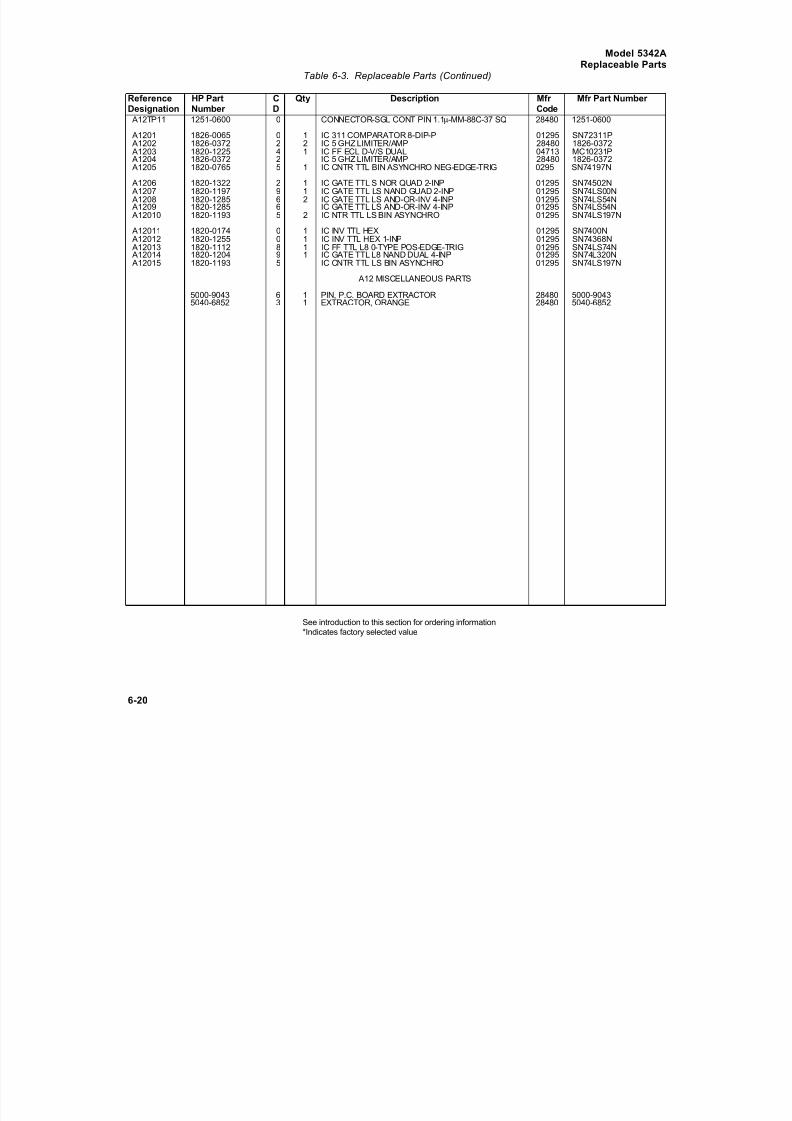
8/21/2019 HP5432 Microwave Frequency Counter
http://slidepdf.com/reader/full/hp5432-microwave-frequency-counter 124/364
Model 5342AReplaceable Parts
Table 6-3. Replaceable Parts (Continued)
Reference HP Part C Qty Description Mfr Mfr Part Number Designation Number D Code A12TP11 1251-0600 0 CONNECTOR-SGL CONT PIN 1.1µ-MM-88C-37 SQ 28480 1251-0600
A1201 1826-0065 0 1 IC 311 COMPARATOR 8-DIP-P 01295 SN72311P A1202 1826-0372 2 2 IC 5 GHZ LIMITER/AMP 28480 1826-0372
A1203 1820-1225 4 1 IC FF ECL D-V/S DUAL 04713 MC10231P A1204 1826-0372 2 IC 5 GHZ LIMITER/AMP 28480 1826-0372 A1205 1820-0765 5 1 IC CNTR TTL BIN ASYNCHRO NEG-EDGE-TRIG 0295 SN74197N
A1206 1820-1322 2 1 IC GATE TTL S NOR QUAD 2-INP 01295 SN74502N A1207 1820-1197 9 1 IC GATE TTL LS NAND GUAD 2-INP 01295 SN74LS00N A1208 1820-1285 6 2 IC GATE TTL LS AND-OR-INV 4-INP 01295 SN74LS54N A1209 1820-1285 6 IC GATE TTL LS AND-OR-INV 4-INP 01295 SN74LS54N A12010 1820-1193 5 2 IC NTR TTL LS BIN ASYNCHRO 01295 SN74LS197N
A12011 1820-0174 0 1 IC INV TTL HEX 01295 SN7400N A12012 1820-1255 0 1 IC INV TTL HEX 1-INP 01295 SN74368N A12013 1820-1112 8 1 IC FF TTL L8 0-TYPE POS-EDGE-TRIG 01295 SN74LS74N A12014 1820-1204 9 1 IC GATE TTL L8 NAND DUAL 4-INP 01295 SN74L320N A12015 1820-1193 5 IC CNTR TTL LS BIN ASYNCHRO 01295 SN74LS197N
A12 MISCELLANEOUS PARTS
5000-9043 6 1 PIN, P.C. BOARD EXTRACTOR 28480 5000-9043
5040-6852 3 1 EXTRACTOR, ORANGE 28480 5040-6852
See introduction to this section for ordering information*Indicates factory selected value
6-20

8/21/2019 HP5432 Microwave Frequency Counter
http://slidepdf.com/reader/full/hp5432-microwave-frequency-counter 125/364
Model 5342AReplaceable Parts
Table 6-3. Replaceable Parts (Continued)
Reference HP Part C Qty Description Mfr Mfr Part Number Designation Number D Code A13 05342-60013 0 1 COUNTER ASSEMBLY (SERIES 1720) 28480 05342-60013 A13C1 0160-3879 7 21 CAPACITOR-FXD .01UF +-20% 100VDC CER 28480 0160-3879 A13C2 0160-3879 7 CAPACITOR-FXD .01UF +-20% 100VDC CER 28480 0160-3879 A13C3 0160-3879 7 CAPACITOR-FXD .01UF +-20% 100VDC CER 28480 0160-3879
A13C4 0160-3879 7 CAPACITOR-FXD .01UF +-20% 100VDC CER 28480 0160-3879 A13C5 0160-3879 7 CAPACITOR-FXD .01UF +-20% 100VDC CER 28480 0160-3879 A13C6 0160-3879 7 CAPACITOR-FXD .01UF +-20% 100VDC CER 28480 0160-3879 A13C7 0160-3879 7 CAPACITOR-FXD .01UF +-20% 100VDC CER 28480 0160-3879 A13C8 0160-3879 7 CAPACITOR-FXD .01UF +-20% 100VDC CER 28480 0160-3879 A13C9 0160-3879 7 CAPACITOR-FXD .01UF +-20% 100VDC CER 28480 0160-3879 A13C10 0160-3879 7 CAPACITOR-FXD .01UF +-20% 100VDC CER 28480 0160-3879 A13C11 0160-3879 7 CAPACITOR-FXD .01UF +-20% 100VDC CER 28480 0160-3879 A13C12 0160-3879 7 CAPACITOR-FXD .01UF +-20% 100VDC CER 28480 0160-3879 A13C13 0160-3879 7 CAPACITOR-FXD .01UF +-20% 100VDC CER 28480 0160-3879 A13C14 0160-3879 7 CAPACITOR-FXD .01UF +-20% 100VDC CER 28480 0160-3879 A13C15 0160-3879 7 CAPACITOR-FXD .01UF +-20% 100VDC CER 28480 0160-3879 A13C16 0160-3879 7 CAPACITOR-FXD .01UF +-20% 100VDC CER 28480 0160-3879 A13C17 0160-3879 7 CAPACITOR-FXD .01UF +-20% 100VDC CER 28480 0160-3879 A13C18 0160-3879 7 CAPACITOR-FXD .01UF +-20% 100VDC CER 28480 0160-3879 A13C19 0160-3879 7 CAPACITOR-FXD .01UF +-20% 100VDC CER 28480 0160-3879 A13C20 0180-1746 5 1 CAPACITOR-FXD 1SUF +-10% 20VDC TA 56289 150D156X9D20H2 A13C21 0160-3879 7 CAPACITOR-FXD .01UF +-20% 100VDC CER 28480 0160-3879 A13C22 0180-0106 9 2 CAPACITOR-FXD 60UF +-20% 6VDC TA 56289 150D606X000682
A13C23 0160-3879 7 CAPACITOR-FXD .01UF +-20% 100VDC CER 28480 0160-3879 A13C25 0180-0106 9 CAPACITOR-FXD 60UF +-20% 6VDC TA 56289 150D606X000682 A13CR1 1901-00400 1 2 DIODE-SWITCHING 30V 50MA 2NS DO-35 28480 1901-0040 A13CR2 1901-0040 1 DIODE-SWITCHING 30V 50MA 2NS DO-35 28480 1901-0040 A13L1 9100-1788 6 2 CHOKE-WIDE BAND ZXAX=680 OHM@ 180 MHZ 02114 VK200 20/48 A13L2 9100-1788 6 CHOKE-WIDE BAND ZXAX=680 OHM@ 180 MHZ 02114 VK200 20/48 A1301 1A54-0071 7 2 TRANSISTOR NPN SI PD=300MN FT=200MHZ 28480 1854-0071 A1302 1854-0071 7 TRANSISTOR NPN SI PD=300MN FT=200MHZ 28480 1854-0071 A13R1 1810-0055 5 2 NETWORK-RES 9-PIN-SIP .15-PIN-SPCG 28480 1810-0055 A13R2 0683-4725 2 6 RESISTOR 4.7K 5% .25W FC TC*-400/4700 01121 084725 A13R3 0683-4725 2 RESISTOR 4.7K 5% .25W FC TC*-400/4700 01121 084725 A13R4 0683-5115 6 4 RESISTOR 510 5% .25W FC TC*-400/4600 01121 085115 A13R5 1810-0055 5 NETWORK-RES 9-PIN-SIP .15-PIN-SPCG 28480 1810-0055 A13R6 0683-2225 3 1 RESISTOR 2.2K 5% .25W FC TC*-400/4700 01121 082225 A13R7 0683-4725 2 RESISTOR 4.7K 5% .25W FC TC*-400/4700 01121 084725 A13R8 0683-4725 2 RESISTOR 4.7K 5% .25W FC TC*-400/4700 01121 084725 A13R9 0683-1025 9 2 RESISTOR 1K 5% .25M FC TC*-400/4600 01121 081025 A13R10 0683-1035 1 6 RESISTOR 10K 5% .25W FC TC*-400/4700 01121 081035 A13R11 0683-4725 2 RESISTOR 4.7K 5% .25W FC TC*-400/4700 01121 084725
A13R12 0683-1635 7 1 RESISTOR 16K 5% .25W FC TC*-400/4800 01121 081635 A13R13 0683-6825 7 4 RESISTOR 6.8K 5% .25W FC TC*-400/4700 01121 086825 A13R14 0683-2735 0 1 RESISTOR 27K 5% .25W FC TC*-400/4800 01121 082735 A13R15 0683-4725 2 RESISTOR 4.7K 5% .25W FC TC*-400/4700 01121 084725 A13R16 0683-1035 1 RESISTOR 10K 5% .25W FC TC*-400/4700 01121 081035 A13R17 0683-6825 7 RESISTOR 6.8K 5% .25W FC TC*-400/4700 01121 086825 A13R18 0683-1035 1 RESISTOR 10K 5% .25W FC TC*-400/4700 01121 081035 A13R19 0683-3915 0 1 RESISTOR 390 5% .25W FC TC*-400/4600 01121 083915 A13R20 0683-1215 9 1 RESISTOR 120 5% .25W FC TC*-400/4600 01121 081215 A13R21 0683-1035 1 RESISTOR 10K 5% .25W FC TC*-400/4700 01121 081035 A13R22 0683-2015 9 1 RESISTOR 200 5% .25W FC TC*-400/4600 01121 082015 A13R23 0683-3325 6 1 RESISTOR 3.3K 5% .25W FC TC*-400/4700 01121 083325 A13R24 0683-5125 8 1 RESISTOR 5.1K 5% .25W FC TC*-400/4700 01121 085125 A13R25 0683-6825 7 RESISTOR 6.8K 5% .25W FC TC*-400/4700 01121 086825 A13R26 0683-6825 7 RESISTOR 6.8K 5% .25W FC TC*-400/4700 01121 086825 A13R27 0683-1035 1 RESISTOR 10K 5% .25W FC TC*-400/4700 01121 081035 A13R28 0683-1035 0 1 RESISTOR 10K 5% .25W FC TC*-400/4700 01121 081035 A13R29 0683-1315 0 1 RESISTOR 130 5% .25W FC TC*-400/4600 01121 081315 A13R30 0683-5115 6 RESISTOR 510 5% .25W FC TC*-400/4600 01121 085115
A13R31 0683-3315 4 1 RESISTOR 330 5% .25W FC TC*-400/4600 01121 083315 A13R32 0683-1025 9 RESISTOR 1K 5% .25W FC TC*-400/4600 01121 081025 A13R33 0683-5115 6 RESISTOR 510 5% .25W FC TC*-400/4600 01121 085115 A13R34 0683-5115 6 RESISTOR 510 5% .25W FC TC*-400/4600 01121 085115 A13TP1 1251-0600 0 8 CONNECTOR-SGL CONT PIN 1.14-MM-BSC-SZ SQ 28480 1251-0600 A13TP2 1251-0600 0 CONNECTOR-SGL CONT PIN 1.14-MM-BSC-SZ SQ 28480 1251-0600 A13TP3 1251-0600 0 CONNECTOR-SGL CONT PIN 1.14-MM-BSC-SZ SQ 28480 1251-0600 A13TP4 1251-0600 0 CONNECTOR-SGL CONT PIN 1.14-MM-BSC-SZ SQ 28480 1251-0600 A13TP5 1251-0600 0 CONNECTOR-SGL CONT PIN 1.14-MM-BSC-SZ SQ 28480 1251-0600
See introduction to this section for ordering information*Indicates factory selected value
6-21

8/21/2019 HP5432 Microwave Frequency Counter
http://slidepdf.com/reader/full/hp5432-microwave-frequency-counter 126/364
Model 5342AReplaceable Parts
Table 6-3. Replaceable Parts (Continued)
Reference HP Part C Qty Description Mfr Mfr Part Number Designation Number D Code
A13TP6 1251-0600 0 CONNECTOR-SGL CONT PIN 1.14-MM-B3C-SZ SQ 28480 1251-0600 A13TP7 1251-0600 0 CONNECTOR-SGL CONT PIN 1.14-MM-BSC-SZ SQ 28480 1251-0600 A13TP8 1251-0600 0 CONNECTOR-SGL CONT PIN 1.14-MM-BSC-SZ SQ 28480 1251-0600
A13U1 1820-0634 7 2 IC CNTR MOS DECD 28480 1820-0634 A13U2 1820-0634 7 IC CNTR MOS DECD 28480 1820-0634 A13U3 1820-1199 1 2 IC INV TTL LS MEX 1-INP01295 SN74LS04N A13U4 1820-1112 8 1 IC FF TTL LS D-TYPE POS-EDGE-TRIG 01295 SN74LS74N A13U5 1820-1238 9 4 IC MUXR/DATA-SEL TTL LS 4-TO-1-LINE DUAL 01295 SN74LS253N A13U6 1820-1238 9 IC MUXR/DATA-SEL TTL LS 4-TO-1-LINE DUAL 01295 SN74LS253N A13U7 1820-1199 1 IC INV TTL LS HEX 1-INP01295 SN74LS804N A13U8 1820-1197 9 1 IC GATE TTL LS NAND QUAD 2-INP 01295 SN74LS00N A13U9 1820-1238 9 IC MUXR/DATA-SEL TTL LS 4-TO-1-LINE DUAL 01295 SN74LS253N A13U10 1820-1238 9 IC MUXR/DATA-SEL TTL LS 4-TO-1-LINE DUAL 01295 SN74LS253N A13U11 1820-1950 2 1 IC GATE ECL OR-NOR 3-INP 04713 MC10212P A13U12 1820-1225 4 2 IC FF ECL D-M’S DUAL 04713 MC10231P A13U13 1820-1251 6 4 IC CNTR TTL LS DECD ASYNCHRO 01295 SN74LS196N A13U14 1820-1251 6 IC CNTR TTL LS DECD ASYNCHRO 01295 SN74LS196N A13U15 1820-1052 5 1 IC XLTR ECL/TTL ECL-TO-TTL QUD 2-INP 04713 MC10125L A13U16 1820-1225 4 IC FF ECL D-M/S DUAL 04713 MC10231P A13U17 1820-1251 6 IC CNTR TTL LS DECD ASYNCHRO 01295 SN74LS196N A13U18 1820-1251 6 IC CNTR TTL LS DECD ASYNCHRO 01295 SN74LS196N
A13 MISCELLANEOUS PARTS5000-9043 6 1 PIN: P.C. BOARD EXTRACTOR 28480 5000-90435040-6852 3 1 EXTRACTOR, ORANGE 28480 5040-6852
See introduction to this section for ordering information*indicates factory selected value
6-22

8/21/2019 HP5432 Microwave Frequency Counter
http://slidepdf.com/reader/full/hp5432-microwave-frequency-counter 127/364
Model 5342AReplaceable Parts
Table 6-3. Replaceable Parts (Continued)
Reference HP Part C Qty Description Mfr Mfr Part Number Designation Number D Code
A14 05342-60014 1 1 PROCESSOR ASSEMBLY (SERIES 1840) 28480 05342-60014
A14C1 0160-3879 7 13 CAPACITOR-FXD .01UF +-20% 100VDC CER 28480 0160-3879 A14C2 0160-3879 7 CAPACITOR-FXD .01UF +-20% 100VDC CER 28480 0160-3879 A14C3 0160-3879 7 CAPACITOR-FXD .01UF +-20% 100VDC CER 28480 0160-3879 A14C4 0160-3879 7 CAPACITOR-FXD .01UF +-20% 100VDC CER 28480 0160-3879 A14C5 0180-0106 9 2 CAPACITOR-FXD 60UF+-20% 6VDC TA 56289 150D606X0006B2 A14C6 0160-3879 7 CAPACITOR-FXD .01UF +-20% 100VDC CER 28480 0160-3879 A14C7 0160-3879 7 CAPACITOR-FXD .01UF +-20% 100VDC CER 28480 0160-3879 A14C8 0160-3879 7 CAPACITOR-FXD .01UF +-20% 100VDC CER 28480 0160-3879 A14C9 0160-3879 7 CAPACITOR-FXD .01UF +-20% 100VDC CER 28480 0160-3879 A14C10 0160-3879 7 CAPACITOR-FXD .01UF +-20% 100VDC CER 28480 0160-3879 A14C11 0160-3879 7 CAPACITOR-FXD .01UF +-20% 100VDC CER 28480 0160-3879 A14C12 0160-3879 7 CAPACITOR-FXD .01UF +-20% 100VDC CER 28480 0160-3879 A14C13 0160-3879 7 CAPACITOR-FXD .01UF +-20% 100VDC CER 28480 0160-3879 A14C14 0160-2743 2 4 CAPACITOR-FXD 33PF +-10% 200VDC CER 28480 0160-2743 A14C15 0160-2743 2 CAPACITOR-FXD 33PF +-10% 200VDC CER 28480 0160-2743 A14C16 0160-2743 2 CAPACITOR-FXD 33PF +-10% 200VDC CER 28480 0160-2743 A14C20 0160-3879 7 CAPACITOR-FXD .01UF +-20% 6VDC TA 28480 0160-3879 A14C21 0160-3651 3 2 CAPACITOR-FXD 68PF +-10% 200VDC CER 28480 0160-3651 A14C22 0160-0106 9 CAPACITOR-FXD 60UF+-20% 6VOC TA 56289 150D606X0006B2 A14C23 0160-3651 3 CAPACITOR-FXD 68PF +-10% 200VDC CER 28480 0160-3651 A14C24 0160-2743 2 CAPACITOR-FXD 33PF +-10% 200VDC CER 28480 0160-2743 A14C25 NOT ASSIGNED 28480 A14C26 0160-3878 6 2 CAPACITOR-FXD 1000PF +-20% 100VDC CER 0160-3878 A14C27 0160-0571 0 1 CAPACITOR-FXD 470PF +-20% 100VDC CER 28480 0160-0571 A14C28 0160-3878 6 CAPACITOR-FXD 100PF +-20% 100VDC CER 28480 0160-3878 A14CR1 1901-0040 1 3 DIODE-SWUTCGUBG 30V 50MA 2NS DO-35 28480 1901-0040 A14CR2 1901-0040 1 DIODE-SWUTCGUBG 30V 50MA 2NS DO-35 28480 1901-0040 A14CR3 1901-0040 1 DIODE-SWUTCGUBG 30V 50MA 2NS DO-35 28480 1901-0040 A14L1 9100-1788 6 1 CHOKE-WIDE BAND 2MAX+680 OHM@ 180 VHZ 02114 VK200 20/48
A14Q1 1854-0574 5 1 TRANSISTOR NPN S1 PO+500MW FT=125MHZ 28480 1854-0574
A14R1 0698-5426 3 4 RESISTOR 10K 10% .125W CC TC=-350/+857 01121 BB1031 A14R2 1810-0055 5 2 NETWORK-RES 9-PIN-SIP .15-PIN-SPCG 28480 1810-0055 A14R3 0698-7027 4 1 RESISTOR 10M 10% .125W CC TC=-666/+1262 01121 BB1061 A14R4 1810-0164 7 1 NETWORK-RES 9-PIN-SIP .15-PIN-SPCG 28480 1810-0164 A14R5 0698-5426 3 RESISTOR 10K 10% .125W CC TC=-350/+857 01121 BB1031 A14R6 1810-0055 5 NETWORK-RES 9-PIN-SIP .15-PIN-SPCG 28480 1800-0055 A14R7 0698-5999 5 4 RESISTOR 4.7K 5% .125W TC=-350/+857 01121 BB4725 A14R8 0698-5999 5 RESISTOR 4.7K 5% .125W TC=-350/+857 01121 BB4725 A14R9 0675-1021 8 5 RESISTOR 1K 10% .125W TC=-330/+800 01121 BB1021 A14R10 0675-1021 8 RESISTOR 1K 10% .125W TC=-330/+800 01121 BB1021 A14R11 0698-5999 5 RESISTOR 4.7K 5% .125W TC=-350/+857 01121 BB4725 A14R12 0698-8127 7 2 RESISTOR 22 5% .125W CC TC=-270/+540 01121 BB2205 A14R13 0675-1021 8 RESISTOR 1K 10% .125W TC=-330/+800 01121 BB1021 A14R14 0698-6283 2 2 RESISTOR 10 5% .125W CC TC=-120/+400 01121 BB1005 A14R15 0698-5426 3 RESISTOR 10K 10% .125W CC TC=-350/+857 01121 BB1031 A14R16 0698-8127 7 RESISTOR 22 5% .125W CC TC=-270/+540 01121 BB2205 A14R17 0675-1021 8 RESISTOR 1K 10% .125W TC=-330/+800 01121 BB1021 A14R18 0698-6283 2 RESISTOR 10 5% .125W CC TC=-120/+400 01121 BB1005 A14R19 0698-5999 5 RESISTOR 4.7K 5% .125W TC=-350/+857 01121 BB4725 A14R20 0698-5426 3 RESISTOR 10K 10% .125W CC TC=-350/+857 01121 BB1031 A14R21 0698-5180 6 1 RESISTOR 2K 5% .125W CC TC=-350/+857 01121 BB2025 A14R22 NOT ASSIGNED A14R23 0698-5562 8 1 RESISTOR 120 5% .125W CC TC=-330/+800 01121 BB1215 A14R24 0675-1021 8 RESISTOR 1K 10% .125W TC=-330/+800 01121 BB1021 A14S1 3101-1856 5 1 SWITCH-SL 8-1A-NS DIP-SLIDE-ASSY .1A 28480 3101-1850 A14S2 3101-1841 8 1 SWITCH-SL 4-1A-NS DIP-SLIDE-ASSY .1A 28480 3101-1841
A14TP1 1251-0600 0 6 CONNECTOR-SGL CONT PIN 1.14-MM-BSC-SZ SQ 28480 1251-0600 A14TP2 1251-0600 0 CONNECTOR-SGL CONT PIN 1.14-MM-BSC-SZ SQ 28480 1251-0600 A14TP3 1251-0600 0 CONNECTOR-SGL CONT PIN 1.14-MM-BSC-SZ SQ 28480 1251-0600 A14TP4 1251-0600 0 CONNECTOR-SGL CONT PIN 1.14-MM-BSC-SZ SQ 28480 1251-0600 A14TP5 1251-0600 0 CONNECTOR-SGL CONT PIN 1.14-MM-BSC-SZ SQ 28480 1251-0600 A14TP6 1251-0600 0 CONNECTOR-SGL CONT PIN 1.14-MM-BSC-SZ SQ 28480 1251-0600
A14U1 1818-0698 8 1 IC ROM MOS 2K x 8 18324 28480 1818-0698 A14U2 1820-1081 0 2 IC DRVR TTL BUS DRVR QUAD 1-INP 18324 NBT26B A14U3 1820-1081 0 IC DRVR TTL BUS DRVR QUAD 1-INP 18324 NBT26B A14U4 1818-0697 7 1 28480 1818-0697 A14U5 1820-1197 9 2 IC GATE TTL LS NAND QUAD 2-INP 01295 8N74LS02N
See introduction to this section for ordering information*Indicates factory selected value 6-23

8/21/2019 HP5432 Microwave Frequency Counter
http://slidepdf.com/reader/full/hp5432-microwave-frequency-counter 128/364
Model 5342A
Replaceable Parts
Table 6-3. Replaceable Parts (Continued)
Reference HP Part C Qty Description Mfr Mfr Part Number Designation Number D Code
A14U6 1820-1144 6 1 IC GATE TTL LS NOR QUAD 2-INP 01295 8N74LS02N A14U7 1818-0706 9 1 IC ROM MOS 3K X 8 28480 1818-0706 A14U8 1820-1255 0 1 IC INV TTL HEX 1-INP 01295 8N74368N
A14U9 1820-1202 7 1 IC GATE TTL LS NAND TPL 3-INP 01295 8474LS10N
A14U10 1820-1199 1 3 IC INV TTL LS HEX 1-INP01295 8N74LS09N A14U11 1820-1425 6 1 IC SCHMITT-TRIG TTL L8 NAND QUAD 2-INP 01295 8N74LS132N A14U12 1818-0135 8 1 IC NMOB 1K NAM STAT 360-NS 3-8 04713 MCM68A10L A14U13 1820-1208 3 1 IC GATE TTL LS OR QUAD 2-INP 01295 8N74LS32N A14U14 1820-1240 3 2 IC DCDR TTL S 3-TO-8-LINE 3-INP 01295 8N74S138N A14U15 1820-1199 1 IC INV TTL LS HEX 1-INP01295 8N74LS04N
A14U16 1820-1368 6 2 1C DRVR TTK BUS DRVR HEX 1-INP 01295 8N74166N A14U17 1820-1072 9 1 IC DCDR TTL S 2-TO-8-LINE DUAL 2-INP 01295 8N748139N A14U18 1820-1368 6 IC DRVR TTL BUS DRVR HEX 1-INP 01295 8N74366N A14U19 1820-1112 8 1 IC FF TTL LS D-TYPE POS-EDGE-TRIG 01295 8N74LS74N A14U20 1820-1240 3 IC DCDR TTL S 3-TO-8-LINE 3-INP 01295 8N74S138N
A14U21 1820-1480 3 1 IC MICPROC NMOS 8-B17 04713 MC6800L A14U22 1820-1197 9 IC GATE TTL LS NAND QUAD 2-INP 01295 8N74LS00N A14U23 1820-1804 5 1 IC DRVR CLOCK DRVR 04713 MP06842 A14U24 1820-1199 1 IC INV TTL LS HEX 1-INP01295 8N74LS04N
A14 MISCELLANEOUS PARTS
1200-0552 4 1 SOCKET-IC 40-CONT DIP-SLDR 28480 1200-05525000-9043 6 1 PIN,P.C. BOARD EXTRACTOR 28480 5000-90435040-6852 3 1 EXTRACTOR, ORANGE 28480 5040-6852
A15 (SEE TABLE 6-8, OPTION 011)
A16 (SEE TABLE 6-5, OPTION 002) ORTABLE 6-6, OPTION 003)
See introduction to this section for ordering information*Indicates factory selected value
6-24

8/21/2019 HP5432 Microwave Frequency Counter
http://slidepdf.com/reader/full/hp5432-microwave-frequency-counter 129/364
Model 5342A
Replaceable Parts
Table 6-3. Replaceable Parts (Continued)
Reference HP Part C Qty Description Mfr Mfr Part Number Designation Number D Code
A17 05342-60017 4 1 TIMING GENERATOR (SERIES 1720) 28480 05342-60017 A17C1 0160-3879 7 26 CAPACITOR-FXD .01UF +-20% 100VDC CER 28480 0160-3879 A17C2 0160-3879 7 CAPACITOR-FXD .01UF +-20% 100VDC CER 28480 0160-3879 A17C3 0160-3879 7 CAPACITOR-FXD .01UF +-20% 100VDC CER 28480 0160-3879 A17C4 0160-3879 7 CAPACITOR-FXD .01UF +-20% 100VDC CER 28480 0160-3879 A17C5 0160-3879 7 CAPACITOR-FXD .01UF +-20% 100VDC CER 28480 0160-3879 A17C6 0160-3879 7 CAPACITOR-FXD .01UF +-20% 100VDC CER 28480 0160-3879 A17C7 0160-3879 7 CAPACITOR-FXD .01UF +-20% 100VDC CER 28480 0160-3879 A17C8 0160-3879 7 CAPACITOR-FXD .01UF +-20% 100VDC CER 28480 0160-3879 A17C9 0160-3879 7 CAPACITOR-FXD .01UF +-20% 100VDC CER 28480 0160-3879 A17C10 0160-3879 7 CAPACITOR-FXD .01UF +-20% 100VDC CER 28480 0160-3879 A17C11 0160-3879 7 CAPACITOR-FXD .01UF +-20% 100VDC CER 28480 0160-3879 A17C12 0160-3879 7 CAPACITOR-FXD .01UF +-20% 100VDC CER 28480 0160-3879 A17C13 0160-3879 7 CAPACITOR-FXD .01UF +-20% 100VDC CER 28480 0160-3879 A17C14 0160-3879 7 CAPACITOR-FXD .01UF +-20% 100VDC CER 28480 0160-3879 A17C15 0160-3879 7 CAPACITOR-FXD .01UF +-20% 100VDC CER 28480 0160-3879 A17C16 0180-0291 3 1 CAPACITOR-FXD 1UF+-10% 35VDC TA 56289 150D105X903582 A17C17 0160-3879 7 CAPACITOR-FXD .01UF +-20% 100VDC CER 28480 0160-3879 A17C18 0180-0106 9 3 CAPACITOR-FXD 60UF+-20% +VDC TA 56289 150D606X000682 A17C19 0160-3879 7 CAPACITOR-FXD .01UF +-20% 100VDC CER 28480 0160-3879
A17CR1 1902-3182 0 1 DIODE-ZNR 12.1V 5% DO-7 PD+.4W TC=+.064% 28480 1902-3182
A17Q1 1854-0560 9 1 TRANSISTOR NPN SI DARL PO=310MW 04713 SPS6740 A17Q2 1853-0036 2 1 TRANSISTOR PNP SI PD=310MW FT=250MHZ 28480 1853-0036
A17R1 0683-1035 1 2 RESISTOR 10K 5% .25W FC TC=-400/+700 01121 CB1035 A17R2 0698-5174 8 1 RESISTOR 200 5% .125W CC TC=-330/+800 01121 BB2015 A17R3 0698-5426 3 5 RESISTOR 10K 10% .125W CC TC=-350/+857 01121 BB1031 A17R4 0698-5426 3 RESISTOR 10K 10% .125W CC TC=-350/+857 01121 BB1031 A17R5 0698-5426 3 RESISTOR 10K 10% .125W CC TC=-350/+857 01121 BB1031 A17R6 0698-5426 3 RESISTOR 10K 10% .125W CC TC=-350/+857 01121 BB1031 A17R7 0675-1021 8 3 RESISTOR 1K 10% .125W CC TC=-330/+800 01121 BB1021 A17R8 0675-1021 8 RESISTOR 1K 10% .125W CC TC=-330/+800 01121 BB1021 A17R9 0698-7102 6 4 RESISTOR 5.1K 5% .125W CC TC=-350/+857 01121 BB5125 A17R10 0698-5181 7 7 RESISTOR 3.6K 5% .125W CC TC=-350/+857 01121 BB3625 A17R11 0698-7102 6 RESISTOR 5.1K 5% .125W CC TC=-350/+857 01121 BB5125 A17R12 0698-5566 2 4 RESISTOR 2.4K 5% .125W CC TC=-350/+857 01121 BB2425 A17R13 0698-7102 6 RESISTOR 5.1K 5% .125W CC TC=-350/+857 01121 BB5125 A17R14 0698-5181 7 RESISTOR 3.6K 5% .125W CC TC=-350/+857 01121 BB3625 A17R15 0698-5566 2 RESISTOR 2.4K 5% .125W CC TC=-350/+857 01121 BB2425
A17R16 0698-5426 3 RESISTOR 10K 10% .125W CC TC=-350/+857 01121 BB1031 A17R17 0698-5181 7 RESISTOR 3.6K 5% .125W CC TC=-350/+857 01121 BB3625 A17R18 0698-5566 2 RESISTOR 2.4K 5% .125W CC TC=-350/+857 01121 BB2425 A17R19 0698-7097 8 1 RESISTOR 1M 5% .125W CC TC=-600/+1137 01121 BB1055 A17R20 0698-5994 0 1 RESISTOR 6.8K 5% .125W CC TC=-350/+857 01121 BB6825 A17R21 0675-1021 8 RESISTOR 1K 10% .125W CC TC=-330/+800 01121 BB1021 A17R22 0698-5999 5 2 RESISTOR 4.7K 5% .125W CC TC=-350/+857 01121 BB4725 A17R23 0698-5999 5 RESISTOR 4.7K 5% .125W CC TC=-350/+857 01121 BB4725 A17R24 0683-1435 1 RESISTOR 10K 5% .25W FC TC=-400/+700 01121 CB1035 A17R25 0698-5566 2 RESISTOR 2.4K 5% .125W CC TC=-350/+857 01121 BB2425 A17R26 0698-5181 7 RESISTOR 3.6K 5% .125W CC TC=-350/+857 01121 BB3625 A17R27 0698-7102 6 RESISTOR 5.1K 5% .125W CC TC=-350/+857 01121 BB5125
A17TP1 1251-0600 0 11 CONNECTOR-SGL CONT PIN 1.14-MM-BSC-SZ SQ 28480 1251-0600 A17TP2 1251-0600 0 CONNECTOR-SGL CONT PIN 1.14-MM-BSC-SZ SQ 28480 1251-0600 A17TP3 1251-0600 0 CONNECTOR-SGL CONT PIN 1.14-MM-BSC-SZ SQ 28480 1251-0600 A17TP4 1251-0600 0 CONNECTOR-SGL CONT PIN 1.14-MM-BSC-SZ SQ 28480 1251-0600 A17TP5 1251-0600 0 CONNECTOR-SGL CONT PIN 1.14-MM-BSC-SZ SQ 28480 1251-0600 A17TP6 1251-0600 0 CONNECTOR-SGL CONT PIN 1.14-MM-BSC-SZ SQ 28480 1251-0600
A17TP7 1251-0600 0 CONNECTOR-SGL CONT PIN 1.14-MM-BSC-SZ SQ 28480 1251-0600 A17TP8 1251-0600 0 CONNECTOR-SGL CONT PIN 1.14-MM-BSC-SZ SQ 28480 1251-0600 A17TP9 1251-0600 0 CONNECTOR-SGL CONT PIN 1.14-MM-BSC-SZ SQ 28480 1251-0600 A17TP10 1251-0600 0 CONNECTOR-SGL CONT PIN 1.14-MM-BSC-SZ SQ 28480 1251-0600
A17U1 1820-1430 3 2 IC CNTR TTL LS BIN SYNCHRO POS-EDGE-TRIG 01295 SN74LS161N A17U2 1820-1430 3 IC CNTR TTL LS BIN SYNCHRO POS-EDGE-TRIG 01295 SN74LS161N A17U3 1820-1197 9 5 IC GATE TTL LS NAND QUAD 2-INP 01295 SN74LS00N A17U4 1820-1433 6 3 IC SHF-RGTR TTL LS R-S SERIAL-IN PRL-OUT 01295 SN74LS164N A17U5 1820-1433 6 IC SHF-RGTR TTL LS R-S SERIAL-IN PRL-OUT 01295 SN74LS164N A17U6 1820-1211 8 1 IC GATE TTL LS NAND QUAD 2-INP 01295 SN74LS86N A17U7 1820-1433 6 IC SHF-RGTR TTL LS R-S SERIAL-IN PRL-OUT 01295 SN74LS164N A17U8 1820-1197 9 IC GATE TTL LS NAND QUAD 2-INP 01295 SN74S00N A17U9 1820-1112 8 2 IC FF TTL LS D-TYPE POS-EDGE-TRIG 01295 SN74LS74N A17U10 1820-1202 7 1 IC GATE TTL LS NAND TPL 3-INP 01295 SN74LS10N
See introduction to this section for ordering information
*Indicates factory selected value 6-25

8/21/2019 HP5432 Microwave Frequency Counter
http://slidepdf.com/reader/full/hp5432-microwave-frequency-counter 130/364
Model 5342A
Replaceable Parts
Table 6-3. Replaceable Parts (Continued)
Reference HP Part C Qty Description Mfr Mfr Part Number Designation Number D Code
A17U11 1820-1442 7 1 ICCNTR TTL LS DECD ASYNCHRO 01295 8N74L8290N A17U12 1820-1197 9 ICGATE TTL LS NAND QUAD 2-INP 01295 8N74L800N A17U13 1820-1197 9 ICGATE TTL LS NAND QUAD 2-INP 01295 8N74L800N A17U14 1820-1197 9 ICGATE TTL LS NAND QUAD 2-INP 01295 8N74L800N A17U15 1820-1112 8 IC FF TTL LS D-TYPE POS-EDGE-TRIG 01295 8N74L800N
A17U16 1820-1180 0 1 IC CNTR MOS 50088 MK5009P A17U17 1820-1225 4 1 IC FF ECL D-M/S DUAL 04713 MC10231P A17U18 1820-1254 9 1 IC BFR TTL NDN-INV HEX 1-INP 27014 DM8095N A17U19 1820-1196 8 1 IC FF TTL LS D-TYPE POS-EDGE-TRIG COM 01295 8N74L8174N A17U20 1820-1255 0 1 IC INV TTL MEX 1-INP 01295 8N74368N
A17 MISCELLANEOUS PARTS
5000-9043 6 2 PIN, P.C. BOARD EXTRACTOR 28480 5000-90035040-6852 3 2 EXTRACTOR, ORANGE 28480 5040-6852
See introduction to this section for ordering information
6-26 *Indicates factory selected value

8/21/2019 HP5432 Microwave Frequency Counter
http://slidepdf.com/reader/full/hp5432-microwave-frequency-counter 131/364
Model 5342A
Replaceable Parts
Table 6-3. Replaceable Parts (Continued)
Reference HP Part C Qty Description Mfr Mfr Part Number Designation Number D Code
A18 05342-60018 5 1 TIME BASE BUFFER ASSEMBLY (SERIES 1720) 28480 05342-60018
A18C1 0180-0106 9 CAPACITOR-FXD 60UF+-20% 6VDC TA 56289 150D066X000682 A18C2 0160-3879 7 CAPACITOR-FXD .01UF +-20% 100VDC CER 28480 0160-3879 A18C3 0160-3879 7 CAPACITOR-FXD .01UF +-20% 100VDC CER 28480 0160-3879 A18C4 0180-0106 9 CAPACITOR-FXD 60UF+-20% 6VDC TA 56289 150D606X000682 A18C5 0160-3879 7 CAPACITOR-FXD .01UF +-20% 100VDC CER 28480 0160-3879
A18C6 0160-3879 7 CAPACITOR-FXD .01UF +-20% 100VDC CER 28480 0160-3879 A18C7 0160-3879 7 CAPACITOR-FXD .01UF +-20% 100VDC CER 28480 0160-3879 A18C8 0160-3879 7 CAPACITOR-FXD .01UF +-20% 100VDC CER 28480 0160-3879 A18C9 0180-1714 7 2 CAPACITOR-FXD 330UF+-10% 6VDC TA 56289 150D337X900682 A18C10 0160-3879 7 CAPACITOR-FXD .01UF +-20% 100VDC CER 28480 0160-3879
A18C11 0160-3879 7 CAPACITOR-FXD .01UF +-20% 100VDC CER 28480 0160-3879 A18C12 0160-3879 7 CAPACITOR-FXD .01UF +-20% 100VDC CER 28480 0160-3879 A18C13 0180-1714 7 CAPACITOR-FXD 330UF+-10% 6VDC TA 56289 150D337X900682
A18CR1 1901-0040 1 2 DIODE-SWITCHING 30V 50MA 2NS DO-35 28480 1901-0040 A18CR2 1901-0040 1 DIODE-SWITCHING 30V 50MA 2NS DO-35 28480 1901-0040
A18L1 9140-0179 1 3 COIL-MLD 22UM 10% Q=75 .155DX.375LG-NDM 28480 9140-0179 A18L2 9140-0179 1 COIL-MLD 22UM 10% Q=75 .155DX.375LG-NDM 28480 9140-0179 A18L3 9140-0179 1 COIL-MLD 22UM 10% Q=75 .155DX.375LG-NDM 28480 9140-0179
A18R1 0698-5178 2 2 RESISTOR 1.5K 5% .125W CC TC=-350/+857 01121 BB1525 A18R2 0698-5181 7 RESISTOR 3.6K 5% .125W CC TC=-350/+857 01121 BB3625 A18R3 0698-5178 2 RESISTOR 1.5K 5% .125W CC TC=-350/+857 01121 BB1525 A18R4 0698-5181 7 RESISTOR 3.6K 5% .125W CC TC=-350/+857 01121 BB3625 A18R5 0698-3113 1 1 RESISTOR 100 5% .125W CC TC=-270/+540 01121 BB1015
A18R6 0690-5181 7 RESISTOR 3.6K 5% .125W CC TC=-350/+857 01121 BB3625
A18TP1 1251-0600 0 CONNECTOR SGL CONT PIN 1.14-MM-BSC-SZ SG 28480 1251-0600
A18U1 1820-0693 8 1 IC FF TTL S D-TYPE POS-EDGE-TRIG 01295 SN74S74N A18U2 1820-1251 6 2 IC CNTR TTL LS DECD ASYNCHRO 01295 SN74LS196N A18U3 1820-1251 6 IC CNTR TTL LS DECD ASYNCHRO 01295 SN74LS196N A18U4 1824-1074 1 1 IC DRVR TTL NOR QUAD 2-INP 01295 SN74128N A18U5 1820-1056 9 1 IC SCHMITT-TRIG TTL NAND QUAD 2-INP 01295 SN74132N
A18 MISCELLANEOUS PARTS
5000-9043 6 PIN,P.C. BOARD EXTRACTOR 28480 5000-90435040-6852 3 EXTRACTRO, ORANGE 28480 5040-6852
See introduction to this section for ordering information
*Indicates factory selected value 6-27

8/21/2019 HP5432 Microwave Frequency Counter
http://slidepdf.com/reader/full/hp5432-microwave-frequency-counter 132/364
Model 5342A
Replaceable Parts
Table 6-3. Replaceable Parts (Continued)
Reference HP Part C Qty Description Mfr Mfr Part Number Designation Number D Code
A19 05342-60019 6 1 PRIMARY POWER ASSEMBLY (SERIES 1720) 28480 05342-60019
A19C1 0180-2802 6 2 CAPACITOR-FXD 140UF+50-10% 250VDC AL 56289 39D147F250M94 A19C2 0180-2802 6 CAPACITOR-FXD 140UF+50-10% 250VDC AL 56289 39D147F250M94 A19C3 0180-2216 4 1 CAPACITOR-FXD 820PF +-5% 300VDC MICA 28480 0160-2216 A19C4 0180-1975 2 2 CAPACITOR-FXD 4UF+50-10% 350VDC AL 56289 390405F350EE4 A19C5 0180-1975 2 CAPACITOR-FXD 4UF+50-10% 350VDC AL 56289 390405F350EE4
A19C6 0180-0106 9 2 CAPACITOR-FXD 60UF+-20% 6VDC TA 56289 150D606X000682 A19C7 0180-0106 9 CAPACITOR-FXD 60UF+-20% 6VDC TA 56289 150D606X000682
A19CR1 1906-0069 4 1 DIODE-FW BRDG 40DV 14 28480 1906-0069 A19CR2 1990-0543 6 1 OPTO-ISOLATOR LED-PXSTR IF=150MA-MAX 28480 1990-0543
A19DS1 2140-0018 0 2 LAMP-GLOW A9A-C 90/58VDC 700UA T-2-BULB 0046G AGA-C A19DS2 2140-0018 0 LAMP-GLOW A9A-C 90/58VDC 700UA T-2-BULB 0046G AGA-C
A19Q1 1854-0311 8 2 TRANSISTOR NPN 2N4240 SI TO-LL PD=35W 01928 2N24240 A19Q2 1854-0311 8 TRANSISTOR NPN 2N4240 SI TO-LL PD=35W 01928 2N4240
A19R1 0686-1045 9 3 RESISTOR 100K 5% .5W CC TC=0+882 01121 E81045 A19R2 0686-1055 1 1 RESISTOR 1M 5% .5W CC TC=0+1000 01121 E81055 A19R3 0686-1045 9 RESISTOR 100K 5% .5W CC TC=0+882 01121 E81045 A19R4 0686-1005 1 3 RESISTOR 10 5% .5W CC TC=0+412 01121 E81005 A19R5 2100-0552 3 1 RESISTOR-TRMR 50 10% C SIDE-ADJ 1-TRN 28480 2100-0552
A19R6 0683-3005 9 1 RESISTOR 30 5% .25W FC TC=-400/+500 01121 C83005 A19R7 0698-0021 4 1 RESISTOR 3.3 10% .5W CC TC=0+412 01121 E83361 A19R8 0813-0001 6 1 RESISTOR 1K 5% 3W PW TC=0+-20 28480 0813-0001 A19R9 0686-1045 9 RESISTOR 100K 5% .5W CC TC=0+882 01121 E81045 A19R10 0686-1005 1 RESISTOR 10 5% .5W CC TC=0+412 01121 E81005
A19R11 0686-1005 1 RESISTOR 10 5% .5W CC TC=0+412 01121 E81005
A19RT1 0839-0006 5 2 THERMISTOR DISC 10-DGN TC=-3.8X/C-DEG 28480 0839-0006 A19RT2 0839-0006 5 THERMISTOR DISC 10-DGN TC=-3.8X/C-DEG 28480 0839-0006
A19RV1 0837-0106 2 2 VARISTOR 150VRMS 28480 0837-0106 A19RV2 0837-0106 2 VARISTOR 150VRMS 28480 0837-0106
A19T1 9100-3066 7 2 TRANSFORMER, POWER 28480 9100-3006
A19T2 9100-3066 7 TRANSFORMER, POWER 28480 9100-3066
A19TP4 1251-0600 0 5 CONNECTOR-SGL CONT PIN 1.14-MM-BSC-SZ SQ 28480 1251-0600 A19TP5 1251-0600 0 CONNECTOR-SGL CONT PIN 1.14-MM-BSC-SZ SQ 28480 1251-0600 A19TP6 1251-0600 0 CONNECTOR-SGL CONT PIN 1.14-MM-BSC-SZ SQ 28480 1251-0600 A19TP7 1251-0600 0 CONNECTOR-SGL CONT PIN 1.14-MM-BSC-SZ SQ 28480 1251-0600 A19TP8 1251-0600 0 CONNECTOR-SGL CONT PIN 1.14-MM-BSC-SZ SQ 28480 1251-0600
A19 MISCELLANEOUS PARTS
0380-0342 9 4 STANDOFF-RVT-ON .125-IN-LG 6-32TMD 00000 ORDER BY DESCRIPTION1205-0085 8 2 HEAT SINK TO-66-PKG 28480 1205-00831400-0486 7 3 BRACKET-RTANG .312-LG X .375-LG .312-WD 28480 1400-04861400-0776 8 1 CABLE TIE .01-4-DIA .19-WD NYL 28480 1400-07767120-1340 6 4 WARNING LABEL 28480 7120-1340
5000-9043 6 1 PIN,P.C. BOARD EXTRACTOR 28480 5000-90435040-6852 3 1 EXTRACTOR, ORANGE 28480 5040-685205342-00019 0 1 SHIELD, PROTECTIVE 28480 05342-00019
See introduction to this section for ordering information
6-28 *Indicates factory selected value

8/21/2019 HP5432 Microwave Frequency Counter
http://slidepdf.com/reader/full/hp5432-microwave-frequency-counter 133/364
Model 5342A
Replaceable Parts
Table 6-3. Replaceable Parts (Continued)
Reference HP Part C Qty Description Mfr Mfr Part Number Designation Number D Code
A20 05342-60020 9 1 SECONDARY POWER ASSEMBLY (SWERIES 1720) 28480 05342-60020
A20C1 0180-1780 7 2 CAPACITOR-FXD 500UF+75-10% 10VDC AL 56289 39D507G010EJ4 A20C2 0160-0576 5 3 CAPACITOR-FXD .10F +-20% 50VDC CER 28480 0160-0576 A20C3 0160-0576 5 CAPACITOR-FXD .10F +-20% 50VDC CER 28480 0160-0576 A20C4 0180-1780 7 CAPACITOR-FXD 500UF+75-10% 10VDC AL 56289 39D507G010EJ4 A20C5 0160-0573 2 1 CAPACITOR-FXD 4700PF +-20% 100VDC CER 28480 0160-0573
A20C6 0180-1746 5 2 CAPACITOR-FXD 15RF+-10% 20VDC TA 56289 150D156X902082 A20C7 0180-0160 5 2 CAPACITOR-FSD 22UF+-20% 35VDC TA 56289 150D226X0035R2 A20C8 0180-1746 5 CAPACITOR-FXD 15RF+-10% 20VDC TA 56289 150D156X902082 A20C9 0180-0160 5 CAPACITOR-FSD 22UF+-20% 35VDC TA 56289 150D226X0035R2 A20C10 0160-0576 5 CAPACITOR-FXD .1UF +-20% 50VDC CER 28480 0160-0576
A20C11 0180-0651 9 2 CAPACITOR-FXD 1700UF+75-10% 10VDC AL 09023 UFT-1700-10 A20C12 0180-0651 9 CAPACITOR-FXD 1700UF+75-10% 10VDC AL 09023 UFT-1700-10
A20CR1 1906-0079 6 1 DIODE-FW BRDG 100V 10A 28480 1906-0079 A20CR2 1906-0051 4 1 DIODE-FW BRDG 100V 1A 28480 1906-0051 A20CR3 1901-0784 0 2 28480 1901-0784 A20CR4 1901-0784 0 28480 1901-0784 A20CR5 1902-0522 6 1 DIODE-ZNR 1N53408 6V 5% PO=5W IF=1UA 04173 1N53408
A20DS1 1990-0485 5 1 LED-VISIBLE LUM-INT=800UCD IF=30MA-MAX 28480 5082-4984
A20L1 9100-3065 6 2 28480 9100-3065 A20L2 9140-0250 9 2 COIL 1MM Z=25 .3125DX,9LG=NDM SOR=100KHZ 28480 9140-0250 A20L3 9140-0250 9 COIL 1MM Z=25 .3125DX,9LG=NDM SOR=100KHZ 28480 9140-0250 A20L4 9100-3065 6 28480 9100-3065 A20L5 9140-0249 6 1 COIL 30UM Q=25 .4DX.875LG-NDM SRF=100KHZ 28480 9140-0249
A20Q1 1826-0214 1 1 IC V RGLTR TD-220 04713 MC7915CT A20Q2 1826-0106 0 1 IC 7815 V RGLTR TO-22004713 MC7815CP
A20R1 0683-4305 4 1 RESISTOR 43 5% .25W FC TC=-400/+500 01121 CB4305 A20R2 0684-0271 7 1 RESISTOR 2.7 10% .25W FC TC=-400/+500 01121 CB27G1 A20R3 0683-1015 7 1 RESISTOR 100 5% .25W FC TC=-400/+500 01121 CB1015
A20T1 9100-3064 5 1 TRANSFORMER, POWER 28480 9100-3064
A20 MISCELLANEOUS PARTS
1205-0219 0 2 HEAT SINK SGL TO-66-PKG 28480 1205-02191251-0400 0 1 CONNECTOR-SGL CONT PIN 1.14-MM-BBC-SZ SG 28480 1251-06003050-0003 3 1 WASHER-FL NM NO. 6 .141-IN-ID .375-IN-00 28480 3050-00033050-0082 8 2 WASHER-FL NM ND. 4 .116-IN-ID .188-IN-00 28480 3050-00825000-9043 6 1 PIN,P.C. BOARD EXTRACTOR 28480 5000-9043
05342-00012 3 2 HEAT SINK, SOLID 28480 05342-000125040-6852 3 1 EXTRACTOR, ORANGE 28480 5040-6852
See introduction to this section for ordering information
*Indicates factory selected value 6-29

8/21/2019 HP5432 Microwave Frequency Counter
http://slidepdf.com/reader/full/hp5432-microwave-frequency-counter 134/364
TM 11-6625-3014-14Model 5342AReplaceable Parts
Table 6-3. Replaceable Parts (Continued)
ReferenceDesignation
HP PartNumber
CD
Qty DescriptionMfr Code
Mfr Part Number
A21 05342-60021 0 1 SWITCH DRIVE ASSEMBLY (SERIES 1804) 28480 05342-60021 A21C1 0180-0229 7 4 CAPACITOR - FXD 33UF+-10% 10VDC TA 56289 150D336X901082 A21C2 0180-0229 7 CAPACITOR - FXD 33UF+-10% 10VDC TA 56289 150D336X901082
A21C3 0180-0159 2 2 CAPACITOR - FXD 220UF+-20% 10VDC TA 56289 150D227X001082 A21C4 0180-0159 2 CAPACITOR - FXD 220UF+-20% 10VDC TA 56289 150D227X001082 A21C5 0180-0229 7 CAPACITOR - FXD 33UF+-10% 10VDC TA 56289 150D336X901082 A21C6 0180-0210 6 4 CAPACITOR - FXD 3.3UF+-20% 15VDC TA 56289 150D335X0015A2 A21C7 0180-0210 6 CAPACITOR - FXD 3.3UF+-20% 15VDC TA 56289 150D335X0015A2 A21C8 0180-0210 6 CAPACITOR - FXD 3.3UF+-20% 15VDC TA 56289 150D335X0015A2 A21C9 0180-0210 6 CAPACITOR - FXD 3.3UF+-20% 15VDC TA 56289 150D335X0015A2 A21C10 0180-1746 5 1 CAPACITOR - FXD 15UF+-10% 20VDC TA 56289 150D156X9020B2 A21C11 0180-1701 2 1 CAPACITOR - FXD 6.8UF+-20% 6VDC TA 56289 150D685X0006A2 A21C12 0180-0197 8 1 CAPACITOR - FXD 2.2UF +-10% 20VDC TA 56289 150D225X9020A2 A21C13 0160-0576 5 2 CAPACITOR - FXD .1UF +-20% 50VDC CER 28480 0160-0576 A21C14 0180-0491 5 1 CAPACITOR - FXD 10UF+-20% 25VDC TA 28480 0180-0491 A21C15 0180-2373 6 3 CAPACITOR - FXD 580UF+150-10% 35VDC AL 28480 0180-2373 A21C16 0180-2373 6 CAPACITOR - FXD 580UF + 150-10% 35VDC AL 28480 0180-2373 A21C17 0160-0576 5 CAPACITOR - FXD .1UF +-20% 50VDC CER 28480 0160-0576 A21C18 0160-3878 6 1 CAPACITOR - FXD 100PF +-20% 100VDC CER 28480 0160-3878 A21C19 0160-0945 2 1 CAPACITOR - FXD 910PF +-5% 100VDC MICA 28480 0160-0945 A21C20 0180-2373 6 CAPACITOR - FXD 580UF +150-10% 35VDC AL 28480 0180-2373 A21C21 0160-0161 4 1 CAPACITOR - FXD .01UF +-10% 200VDC POLYE 28480 0160-0161
A21C22 0180-0229 7 CAPACITOR - FXD 33UF +-10% 10VDC TA 56289 150D336X9010B2 A21CR1 1902-0522 6 2 DIODE - ZNR 1N5340B 6V 5% PD=5W IR=1UA 04713 1N5340B A21CR2 1906-0096 7 1 DIODE - FW BRDG 200V 2A 04713 MDA202 A21CR3 1902-0522 6 DIODE - ZNR 1N5340B 6V 5% PD=5W IR=1UA 04713 1N5340B A21CR4 1902-0644 3 1 DIODE - ZNR 1N5363B 30V 5% PD=5W TC=+29MV 28480 1902-0644 A21CR5 1901-0040 1 1 DIODE - SWITCHING 30V 50MA 2NS DO-35 28480 1901-0040 A21DS1 1990-0486 6 1 LED - VISIBLE LUM - INT=1MCD IF=20MA-MAX 28480 5082-4684 A21L1 9100-2276 9 1 COIL-MLD 100UH 10% Q=50 .095DX .25 LG - NOM 28480 9100-2276 A21Q1 1854-0635 9 1 TRANSISTOR NPN SI PD=50W 03508 D44H5 A21Q2 1854-0634 8 1 TRANSISTOR NPN SI PD=1W FT=50MHZ 04713 MPS-U01 A21Q3 1854-0215 1 2 TRANSISTOR NPN SI PD=350MW FT=300MHZ 04713 SPS 3611 A21Q4 1853-0326 3 1 TRANSISTOR PNP SI PD=1W FT=50MHZ 28480 1853-0326 A21Q5 1853-0036 2 1 TRANSISTOR PNP SI PD=310MW FT=250MHZ 28480 1853-0036 A21Q6 1853-0363 8 1 TRANSISTOR PNP SI PD=50W 03508 X45H281 A21Q7 1826-0275 4 2 IC 78L12A V RGLTR TO-92 04713 MC78L12ACP A21Q8 1826-0275 4 IC 78L12A V RGLTR TO-92 04713 MC78L12ACP A21Q9 1854-0246 8 2 TRANSISTOR NPN SI PD=350MW FT=250MHZ 04713 SPS 233 A21Q10 1853-0058 8 2 TRANSISTOR PNP SI PD=300MW FT=200MHZ 07263 S32248 A21Q11 1854-0246 8 TRANSISTOR NPN SI PD=350MW FT=250MHZ 04713 SPS 233
A21Q12 1853-0058 8 TRANSISTOR PNP SI PD=300MW FT=200MHZ 07263 S32248 A21Q13 1854-0215 1 TRANSISTOR NPN SI PD=350MW FT=300MHZ 04713 SPS 3611 A21R1 0757-0419 0 5 RESISTOR 681 1% .125W F TC=0+-100 24546 C4-1/8-T0-681R-F A21R2 0757-0417 8 1 RESISTOR 562 1% .125W F TC=0+-100 24546 C4-1/8-T0-562R-F A21R3 0698-3441 8 3 RESISTOR 215 1% .125W F TC=0+-100 24546 C4-1/8-T0-215R-F A21R4 0757-0419 0 RESISTOR 681 1% .125W F TC=0+-100 24546 C4-1/8-T0-681R-F A21R5 0757-0419 0 RESISTOR 681 1% .125W F TC=0+-100 24546 C4-1/8-T0-681R-F A21R6 0698-3155 1 5 RESISTOR 4.64K 1% .125W F TC=0+-100 24546 C4-1/8-T0-4641-F A21R7 0698-5808 5 1 RESISTOR 4K 1% .125W F TC=0+-100 24546 C4-1/8-T0-4001-F A21R8 0698-3444 1 1 RESISTOR 316 1% .125W F TC= 0+-100 24546 C4-1/8-T0-316R-F A21R9 0811-1827 2 2 RESISTOR .1 10% 3W PW TC=0+-90 28480 0811-1827 A21R10 0757-0419 0 RESISTOR 681 1% .125W F TC=0+-100 24546 C4-1/8-T0-681R-F A21R11 0698-3155 1 RESISTOR 4.64K 1% .125W F TC=0+-100 24546 C4-1/8-T0-4641-F A21R12 0811-1827 2 RESISTOR .1 10% 3W PW TC=0+-90 28480 0811-1827 A21R13 0757-0346 2 1 RESISTOR 10 1% .125W F TC=0+-100 24546 C4-1/8-T0-10R0-F A21R14 0698-3441 8 RESISTOR 215 1% .125W F TC= 0+-100 24546 C4-1/8-T0-215R-F A21R15 0698-3441 8 RESISTOR 215 1% .125W F TC= 0+-100 24546 C4-1/8-T0-215R-F A21R16 0698-0082 7 2 RESISTOR 464 1% .125W F TC=0+-100 24546 C4-1/8-T0-4640-F A21R17 2100-3154 7 1 RESISTOR-TRMR 1K 10% C SIDE-ADJ 17-TRN 02111 43P102
A21R18 0757-0465 6 3 RESISTOR 100K 1% .125W F TC=0+-100 24546 C4-1/8-T0-1003-F A21R19 0698-0084 9 3 RESISTOR 2.15K 1% .125W F TC=0+-100 24546 C4-1/8-T0-2151-F A21R20 0757-0280 3 2 RESISTOR 1K 1% .125W F TC=0+-100 24546 C4-1/8-T0-1001-F A21R21 0698-0082 7 RESISTOR 464 1% .125W F TC=0+-100 24546 C4-1/8-T0-4640-F A21R22 0757-0280 3 RESISTOR 1K 1% .125W F TC=+-100 24546 C4-1/8-T0-1001-F A21R23 0698-3155 1 RESISTOR 4.64K 1% .125W F TC=0+-100 24546 C4-1/8-T0-4641-F A21R24 0698-3155 1 RESISTOR 4.64K 1% .125W F TC=0+-100 24546 C4-1/8-T0-4641-F A21R25 0757-0465 6 RESISTOR 100K 1% .125W F TC=+-100 24546 C4-1/8-T0-1003-F A21R26 0698-3150 6 2 RESISTOR 2.37K 1% .125W F TC=0+-100 24546 C4-1/8-T0-2371-F A21R27 2100-3211 7 1 RESISTOR-TRMR 1K 10% C TOP-ADJ 1-TRN 28480 2100-3211 A21R28 0757-0419 0 RESISTOR 681 1% .125W F TC=0+-100 24546 C4-1/8-T0-681R-F A21R29 0698-3150 6 RESISTOR 2.37K 1% .125W F TC=0+-100 24546 C4-1/8-T0-2371-F A21R30 0698-0084 9 RESISTOR 2.15K 1% .125W F TC=0+-100 24546 C4-1/8-T0-2151-F
See introduction to this section for ordering information*Indicates factory selected value
6-30

8/21/2019 HP5432 Microwave Frequency Counter
http://slidepdf.com/reader/full/hp5432-microwave-frequency-counter 135/364
Model 5342A
Replaceable Parts
Table 6-3. Replaceable Parts (Continued)
Reference HP Part C Qty Description Mfr Mfr Part Number Designation Number D Code
A21R31 0698-0084 9 RESISTOR 2.15K 1% .125W F TC=0+-100 24546 CW-1/8-TO-2151-F A21R33 0757-0465 6 RESISTOR 100K 1% .125W F TC=0+-100 24546 CW-1/8-TO-1003-F A21R37 0698-3155 1 RESISTOR 4.60K 1% .125W F TC=0+-100 24546 CW-1/8-TO-4641-F
A21TP1 1251-0600 0 11 CONNECTOR-SGL CONT PIN 1.14-MM-BSC-SZ SQ 28480 1251-0600 A21TP2 1251-0600 0 CONNECTOR-SGL CONT PIN 1.14-MM-BSC-SZ SQ 28480 1251-0600 A21TP3 1251-0600 0 CONNECTOR-SGL CONT PIN 1.14-MM-BSC-SZ SQ 28480 1251-0600 A21TP4 1251-0600 0 CONNECTOR-SGL CONT PIN 1.14-MM-BSC-SZ SQ 28480 1251-0600
A21U1 1820-0493 6 2 IC OP AMP 8-DIP-P 27014 LM307N A21U2 1820-0493 6 IC OP AMP 8-DIP-P 27014 LM307N A21U3 1826-0355 1 1 IC 555 8-DIP-P 28480 182640355 A21U4 1826-0428 9 1 IC 3524 MODULATOR 16-DIP-C 01295 SG3524J
A21 MISCELLANEOUS PARTS
1205-0273 2 2 HEAT SINK SGL PLSTC-PWR-PXG 28480 1205-02735000-9043 1 1 PIN,P.C. BOARD EXTRACTOR 28480 5000-90435040-6852 1 1 EXTRACTOR, ORANGE 28480 5040-6852
See introduction to this section for ordering information
*Indicates factory selected value 6-31

8/21/2019 HP5432 Microwave Frequency Counter
http://slidepdf.com/reader/full/hp5432-microwave-frequency-counter 136/364
Model 5342A
Replaceable Parts
Table 6-3. Replaceable Parts (Continued)
Reference HP Part C Qty Description Mfr Mfr Part Number Designation Number D Code
A22 05342-60022 1 1 MOTHERBOARD ASSEMBLY (SERIES 1720) 28480 05342-60022
A22J1 1200-0785 5 2 SOCKET-IC 24-CONT DIP DIP-SLDR 28480 1200-0785 A22J2 1200-0785 5 SOCKET-IC 24-CONT DIP DIP-SLDR 28480 1200-0785
A22Y1 9100-3067 8 1 TRANSFORMER, POWER 28480 9100-3067
A22W1 05342-60102 8 1 CABLE ASSEMBLY, 1.0 MAG 28480 05342-60102 A22W2 05342-60121 1 1 CABLE ASSEMBLY, LF MB 28480 05342-60121 A22W3 05342-60103 8 1 CABLE ASSEMBLY, IF INT 28480 05342-60103 A22W4 05342-60109 5 1 CABLE ASSEMBLY, MICRO INT 28480 05342-60109 A22W5 05342-60104 0 1 CABLE ASSEMBLY, SHIELD 28480 05342-60104
A22W6 05342-60112 0 1 CABLE ASSEMBLY, SHIELD 28480 05342-60112 A22W7 05342-60111 9 1 CABLE ASSEMBLY, POWER 28480 05342-60111
(INCLUDES LINE SWITCH)
A22XA3 1251-1626 2 5 CONNECTOR-PC EDGE 12-CONT/ROW 2-ROWS 28480 1251-1626 A22XA4 1251-2034 8 CONNECTOR-PC EDGE 10-CONT/ROW 2-ROWS 28480 1251-2034 A22XA5 1251-2034 8 CONNECTOR-PC EDGE 10-CONT/ROW 2-ROWS 28480 1251-2034 A22XA6 1251-2034 8 CONNECTOR-PC EDGE 10-CONT/ROW 2-ROWS 28480 1251-2034 A22XA7 1251-1626 2 CONNECTOR-PC EDGE 12-CONT/ROW 2-ROWS 28480 1251-1626
A22XA8 1251-1626 2 CONNECTOR-PC EDGE 12-CONT/ROW 2-ROWS 28480 1251-1626 A22XA9 1251-1626 2 CONNECTOR-PC EDGE 12-CONT/ROW 2-ROWS 28480 1251-1626 A22XA10 1251-1365 6 5 CONNECTOR-PC EDGE 22-CONT/ROW 2-ROWS 28480 1251-1365 A22XA11 1251-1626 2 CONNECTOR-PC EDGE 12-CONT/ROW 2-ROWS 28480 1251-1626 A22XA12 1251-1365 6 CONNECTOR-PC EDGE 22-CONT/ROW 2-ROWS 28480 1251-1365
A22XA13 1251-1365 6 CONNECTOR-PC EDGE 22-CONT/ROW 2-ROWS 28480 1251-1365 A22XA14A 1251-2026 8 6 CONNECTOR-PC EDGE 18-CONT/ROW 2-ROWS 28480 1251-2026 A22XA14B 1251-2026 8 CONNECTOR-PC EDGE 18-CONT/ROW 2-ROWS 28480 1251-2026 A22XA15A 1251-2026 8 CONNECTOR-PC EDGE 18-CONT/ROW 2-ROWS 28480 1251-2026 A22XA15B 1251-2026 8 CONNECTOR-PC EDGE 18-CONT/ROW 2-ROWS 28480 1251-2026
A22XA16 1251-2026 8 CONNECTOR-PC EDGE 18-CONT/ROW 2-ROWS 28480 1251-2026 A22XA16B 1251-2034 8 6 CONNECTOR-PC EDGE 10-CONT/ROW 2-ROWS 28480 1251-2034 A22XA17 1251-2026 8 CONNECTOR-PC EDGE 18-CONT/ROW 2-ROWS 28480 1251-2026 A22XA18 1251-2034 8 CONNECTOR-PC EDGE 10-CONT/ROW 2-ROWS 28480 1251-2034 A22XA19 1251-2582 1 1 CONNECTOR-PC EDGE 24-CONT/ROW 2-ROWS 28480 1251-2582
A22XA20 1251-1365 6 CONNECTOR-PC EDGE 22-CONT/ROW 2-ROWS 28480 1251-1365 A22XA21 1251-1365 6 CONNECTOR-PC EDGE 22-CONT/ROW 2-ROWS 28480 1251-1365 A22XA24 1251-2034 8 CONNECTOR-PC EDGE 10-CONT/ROW 2-ROWS 28480 1251-2034
0380-0383 8 5 STANDOFF-RVT-ON .125-IN-LG 6-32-THQ 28480 ORDER BY DESCRIPTION1251-2205 5 2 POLARIZING KEY-PC EDGE CONN 28480 1251-22055040-0170 6 1 GUIDE, PLUG-IN PC BOARD 28480 5040-0170
A23 0960-0400 2 1 POWER MODULE, UNFILTERED 28480 0960-0444
A24 05341-60047 9 1 10 MHZ OSCILLATOR ASSY (SERIES 1804) 28480 05341-60047
A24C1 0160-2143 6 1 CAPACITOR-FXD 2000PF +80-20% 1MVDC CER 28480 0160-2143 A24C2 0180-0552 9 1 CAPACITOR-FXD 220UF+-20% 10VDC TA 28480 0180-0552
A24L1 9100-2430 7 1 COIL-MLD 220UM 10% Q=55 .156DX.375LG-NOM 28480 9100-2430
A24Y1 0960-0394 1 1 CRYSTAL 28480 0960-0394
See introduction to this section for ordering information
6-32 *Indicates factory selected value

8/21/2019 HP5432 Microwave Frequency Counter
http://slidepdf.com/reader/full/hp5432-microwave-frequency-counter 137/364
Model 5342AReplaceable Parts
Table 6-3. Replaceable Parts (Continued)
Reference HP Part C Qty Description Mfr Mfr Part Number
Designation Number D Code A25 05342-60025 4 1 PREAMPLIFIER ASSEMBLY (SERIES 1804) 28480 05342-60025 A25C1 0180-0230 0 4 CAPACITOR-FXD 1UF+-20% 50VDC TA 56289 150D105X0050A2 A25C2 0160-3879 7 15 CAPACITOR-FXD .01UF +-20% 100VDC CER 28480 0160-3879 A25C3 0160-3879 7 CAPACITOR-FXD .01UF +-20% 100VDC CER 28480 0160-3879 A25C4 0160-3879 7 CAPACITOR-FXD .01UF +-20% 100VDC CER 28480 0160-3879 A25C5 0160-3879 7 CAPACITOR-FXD .01UF +-20% 100VDC CER 28480 0160-3879 A25C6 0160-3879 7 CAPACITOR-FXD .01UF +-20% 100VDC CER 28480 0160-3879 A25C7 0160-3879 7 CAPACITOR-FXD .01UF +-20% 100VDC CER 28480 0160-3879 A25C8 0160-3879 7 CAPACITOR-FXD .01UF +-20% 100VDC CER 28480 0160-3879 A25C9 0160-3879 7 CAPACITOR-FXD .01UF +-20% 100VDC CER 28480 0160-3879 A25C10 0160-2263 1 1 CAPACITOR-FXD 13PF +-5% 500VDC CER 0+-30 28480 0160-2263 A25C11 0121-0445 5 1 CAPCITOR-V TRMR-CER 4.5-20PF 160V 28480 0121-0445 A25C12 0180-0230 0 CAPACITOR-FXD 1UF+-20% 50VDC TA 56289 150D105X0050A2 A25C13 0160-3879 7 CAPACITOR-FXD .01UF +-20% 100VDC CER 28480 0160-3879 A25C14 0160-3879 7 CAPACITOR-FXD .01UF +-20% 100VDC CER 28480 0160-3879 A25C15 0160-3879 7 CAPACITOR-FXD .01UF +-20% 100VDC CER 28480 0160-3879 A25C16 0160-3878 6 1 CAPACITOR-FXD .01UF +-20% 100VDC CER 28480 0160-3878 A25C17 0160-2260 8 2 CAPACITOR-FXD 13PF +-5% 500VDC CER 0+-30 28480 0160-2260 A25C18 0160-2265 3 1 CAPACITOR-FXD 13PF +-5% 500VDC CER 0+-30 28480 0160-2265 A25C19 0160-2260 8 CAPACITOR-FXD 13PF +-5% 500VDC CER 0+-30 28480 0160-2260 A25C20 0160-0576 5 1 CAPACITOR-FXD .1UF +-20% 50VDC CER 28480 0160-0576 A25C21 0160-3879 7 CAPACITOR-FXD .01UF +-20% 100VDC CER 28480 0160-3879 A25C22 0160-3879 7 CAPACITOR-FXD .01UF +-20% 100VDC CER 28480 0160-3879 A25C23 0160-3879 7 CAPACITOR-FXD .01UF +-20% 100VDC CER 28480 0160-3879 A25C24 0180-0230 0 CAPACITOR-FXD 1UF+-20% 50VDC TA 56289 150D105X0050A2 A25C25 0180-0230 0 CAPACITOR-FXD 1UF+-20% 50VDC TA 56289 150D105X0050A2 A25C26 0160-3879 7 CAPACITOR-FXD .01UF +-20% 100VDC CER 28480 0160-3879 A25C27 0160-4082 6 8 CAPACITOR-FDTHRU 100PF 20% 200V CER 28480 0160-4082 A25C28 0160-4082 6 CAPACITOR-FDTHRU 100PF 20% 200V CER 28480 0160-4082 A25C29 0160-4082 6 CAPACITOR-FDTHRU 100PF 20% 200V CER 28480 0160-4082 A25C30 0160-4082 6 CAPACITOR-FDTHRU 100PF 20% 200V CER 28480 0160-4082 A25C31 0160-4082 6 CAPACITOR-FDTHRU 100PF 20% 200V CER 28480 0160-4082 A25C32 0160-4082 6 CAPACITOR-FDTHRU 100PF 20% 200V CER 28480 0160-4082 A25C33 0160-4082 6 CAPACITOR-FDTHRU 100PF 20% 200V CER 28480 0160-4082 A25C34 0160-4082 6 CAPACITOR-FDTHRU 100PF 20% 200V CER 28480 0160-4082 A25C35 0160-3029 9 2 CAPACITOR-FXD 7.5PF +-.5PF 100VDC CER 28480 0160-3029 A25C36 0160-3029 9 CAPACITOR-FXD 7.5PF +-.5PF 100VDC CER 28480 0160-3029 A25CR1 1901-0535 9 2 DIODE-SCHOTTKY 28480 1901-0535 A25CR2 1901-0535 9 DIODE-SCHOTTKY 28480 1901-0535 A25CR3 1901-0040 1 3 DIODE-SWITCHING 30V 50MA 2NS DD-35 28480 1901-0040 A25CR4 1901-0040 1 DIODE-SWITCHING 30V 50MA 2NS DD-35 28480 1901-0040
A25CR5 1901-0040 1 DIODE-SWITCHING 30V 50MA 2NS DD-35 28480 1901-0040
A25L1 05342-80002 9 4 COI, 3-TURNS 28480 05342-80002 A25L 05342-80002 9 COI, 3-TURNS 28480 05342-80002 A25L3 9100-0346 0 3 COIL-MLD 50NH 20% Q=40 .095DX.25LG-NOM 28480 9100-0346 A25L4 9100-0346 0 COIL-MLD 50NH 20% Q=40 .095DX.25LG-NOM 28480 9100-0346 A25L5 05342-80002 9 COI, 3-TURNS 28480 05342-80002 A25L6 05342-80002 9 COI, 3-TURNS 28480 05342-80002 A25L7 9100-0346 0 COIL-MLD 50NH 20% Q=40 .095DX.25LG-NOM 28480 9100-0346 A25L8 9100-2265 6 4 COIL-MLD 10UH 20% Q=40 .095DX.25LG-NOM 28480 9100-2265 A25L9 9100-2265 6 COIL-MLD 10UH 20% Q=40 .095DX.25LG-NOM 28480 9100-2265 A25L10 9100-2247 4 3 COIL-MLD 100NH 20% Q=40 .095DX.25LG-NOM 28480 9100-2247 A25L11 9100-2247 4 COIL-MLD 100NH 20% Q=40 .095DX.25LG-NOM 28480 9100-2247 A25L12 9100-2247 4 COIL-MLD 100NH 20% Q=40 .095DX.25LG-NOM 28480 9100-2247 A25L13 9100-2265 6 COIL-MLD 10UH 20% Q=40 .095DX.25LG-NOM 28480 9100-2265 A25L14 9100-2265 6 COIL-MLD 10UH 20% Q=40 .095DX.25LG-NOM 28480 9100-2265
A25Q1 1854-0591 6 2 TRANSISTOR NPN SI PO=180MW FT=4GHZ 25403 8FR-90 A25Q2 1854-0591 6 TRANSISTOR NPN SI PO=180MW FT=4GHZ 25403 8FR-90
A25Q3 1854-0071 7 2 TRANSISTOR NPN SI PO=300MW FT=200MHZ 28480 1854-0071 A25Q4 1854-0071 7 TRANSISTOR NPN SI PO=300MW FT=200MHZ 28480 18544-0071 A25Q5 1853-0058 8 1 TRANSISTOR PNP SI PO=300MW FT=200MHZ 07263 832248 A25Q6 1853-0020 4 1 TRANSISTOR PNP SI PO=300MW FT=150MHZ 28480 1853-0020 A25R1 0698-3113 1 3 RESISTOR 100 5% .125W CC TC=-270/+540 01121 BB1015 A25R2 0698-5176 0 2 RESISTOR 510 5% .125W CC TC=-330/+800 01121 BB5115 A25R3 0675-1021 8 1 RESISTOR 1K 10% .125W CC TC=-330/+800 01121 BB1021 A25R4 0698-3114 2 1 RESISTOR 300 5% .125W CC TC=-330/+800 01121 BB5015 A25R5 0698-8073 2 1 RESISTOR 1.6K 5% .125W CC TC=-350/+857 01121 BB1625 A25R6 0698-8354 2 1 RESISTOR 270 5% .125W CC TC=-330/+800 01121 BB2715 A25R7 0698-6000 1 1 RESISTOR 2.7K 5% .125W CC TC=-350/+857 01121 BB2725 A25R8 0698-6123 9 1 RESISTOR 20K 5% .125W CC TC=-466/+875 01121 BB2035 A25R9 0698-6681 4 2 RESISTOR 9.1 5% .125W CC TC=-120/+400 01121 BB91G5 A25R10 05342-80004 1 4 RESISTOR, MODIFIED 28480 05342-80004
See introduction to this section for ordering information*Indicates factory selected value
6-33

8/21/2019 HP5432 Microwave Frequency Counter
http://slidepdf.com/reader/full/hp5432-microwave-frequency-counter 138/364
Model 5342AReplaceable Parts
Table 6-3. Replaceable Parts (Continued)
Reference HP Part C Qty Description Mfr Mfr Part Number Designation Number D Code
A25R11 05342-80004 1 RESISTOR, MODIFIED 28480 05342-80004 A25R12 0698-5996 2 2 RESISTOR 560 5% .125W CC TC=-330/+800 01121 BB5615
A25R13 05342-80004 1 RESISTOR, MODIFIED 28480 05342-80004 A25R14 05342-80004 1 RESISTOR, MODIFIED 28480 05342-80004 A25R15 0698-5996 2 RESISTOR 560 5% .125W CC TC=-330/+800 01121 BB5615
A25R16 0698-5075 8 1 RESISTOR 130 5% .125W CC TC=-330/+800 01121 BB1315 A25R17 0698-6681 4 RESISTOR 9.1 5% .125W CC TC=-120/+400 01121 BB9165 A25R18 0698-311 9 2 RESISTOR 30 5% .125W CC TC=-270/+540 01121 BB3005 A25R19 0757-0399 5 1 RESISTOR 82.5 1% .125W F TC=0+-100 24546 C4-1/8-T0-82R5-F A25R20 0698-3113 1 RESISTOR 100 5% .125W CC TC=-270/+500 01121 BB1015
A25R21 0698-5562 8 2 RESISTOR 120 5% .125W CC TC=-330/+800 01121 BB1215 A25R22 0757-0180 2 1 RESISTOR 31.6 1% .125W F TC=0+-100 28480 0757-0180 A25R23 0757-0038 3 1 RESISTOR 5.11K 1% .125W F TC=0+-100 24546 C4-1/8-70-5111-F A25R24 0698-3113 1 RESISTOR 100 5% .125W CC TC=-270/+540 01121 BB1015 A25R25 0698-3111 9 RESISTOR 30 5% .125W CC TC=-270/+540 01121 BB3005
A25R26 0698-3378 0 1 RESISTOR 51 5% .125W CC TC=-270/+540 01121 BB5105 A25R27 0698-5562 8 RESISTOR 120 5% .125W CC TC=-330/+800 01121 BB1215 A25R28 2100-3207 1 1 RESISTOR-TRMR 5K 10% C SIDE-ADJ 1-TRM 28480 2100-3207
A25R29 0757-0485 0 2 RESISTOR 681K 1% .125W F TC=0+-100 28480 0757-0485 A25R30 0757-0485 0 RESISTOR 681K 1% .125W F TC=0+-100 28480 0757-0485
A25R31 2100-3274 2 1 RESISTOR-TRMR 10K 10% C SIDE-ADJ 1-TRN 28480 2100-3274 A25R32 0757-0469 0 1 RESISTOR 150K 1% .125W F TC=0+-100 24546 C4-1/8-T0-1503-F A25R33 0698-7966 0 1 RESISTOR 680K 5% .125W CC TC=-60/+1137 01121 BB6845 A25R34 0698-5176 0 RESISTOR 510 5% .125W CC TC=-330/+800 01121 BB5115 A25R35 0698-7241 4 1 RESISTOR 1.62K 1% .05W F TC=0+-100 28480 0698-7241
A25R36 0757-0027 6 1 RESISTOR 365 1% .5W F TC=0+-25 28480 0757-0027 A25R37 0698-7259 4 2 RESISTOR 9.09K 1% .05W F TC=0+-100 24546 C3-1/8-T0-9091-G A25R38 0698-7253 8 3 RESISTOR 5.11K 1% .05W F TC=0+-100 24546 C3-1/8-T0-5111-G A25R39 0698-7259 4 RESISTOR 9.09K 1% .05W F TC=0+-100 24546 C3-1/8-T0-9091-G A25R40 0698-7253 8 RESISTOR 5.11K 1% .05W F TC=0+-100 24546 C3-1/8-T0-5111-G
A25R41 0698-7250 5 1 RESISTOR 3.83K 1% .05W F TC=0+-100 24546 C3-1/8-T0-3831-G A25R42 0698-7253 8 RESISTOR 5.11K 1% .05W F TC=0+-100 24546 C3-1/8-T0-5111-G A25R43 0698-7243 6 1 RESISTOR 1.96K 1% .05W F TC=0+-100 24546 C3-1/8-T0-1961-G A25R44 0698-5994 0 1 RESISTOR 6.8K 5% .125W CC TC=-350/+857 01121 BB6825
A25R45 0698-8373 5 1 RESISTOR 470K 5% .125W CC TC=-600/+1137 01121 BB4745 A25TP1 1251-0600 0 4 CONNECTOR-SGL CONT PIN 1.114-MM-BSC-SZ SQ 28480 1251-0600 A25TP2 1251-0600 0 CONNECTOR-SGL CONT PIN 1.114-MM-BSC-SZ SQ 28480 1251-0600 A25TP3 1251-0600 0 CONNECTOR-SGL CONT PIN 1.114-MM-BSC-SZ SQ 28480 1251-0600 A25TP4 1251-0600 0 CONNECTOR-SGL CONT PIN 1.114-MM-BSC-SZ SQ 28480 1251-0600
A25U1 1826-0372 2 2 IC 5 GHZ LIMITER/AMP 28480 1826-0372 A25U2 1826-0372 2 IC 5 GHZ LIMITER/AMP 28480 1826-0372 A25U3 1826-0065 0 1 IC 311 COMPARTOR 8-DIP-P 01295 8N72311P A25U4 1826-0054 5 1 IC GATE TTL NAND QUAD 2-INP 01295 8N7400N
A25W1 05342-60108 4 1 CABLE ASSEMBLY, RF 28480 05342-60108 A25W2 05342-60107 3 2 CABLE ASSEMBLY, PREAMP/DRIVER 28480 05342-60107 A25W3 05342-60107 3 CABLE ASSEMBLY, PREAMP/DRIVER 28480 05342-60107
A25 MISCELLANEOUS PARTS
1200-0647 8 1 SOCKET-XSTR 3-CONT TO-18 DIP-SLDR 28480 1200-06471250-0901 2 2 CONNECTOR-RF SMB M SGL-HOLE-FR 50-DNM 28480 1250-09011400-0486 7 3 BRACKET-RTANG .312-LG X .375-LG .312-WD 28480 1400-04862190-0033 4 1 WASHER-LK INTL 7 5/16 IN .314-IN-ID 28480 2190-00332950-0007 4 1 NUT-HEX-DBL-CHAM 5/16-32-THD .094-IN-TMK 00000 ORDER BY DESCRIPTION
05342-00006 5 1 COVER, PREAMPLIFIER28480 05342-0000605342-00007 6 1 BRACKET, SAMPLER 28480 05342-0000705342-20103 5 1 SHELL, CONNECTOR 28480 05342-20103
See introduction to this section for ordering information*Indicates factory selected value
6-34

8/21/2019 HP5432 Microwave Frequency Counter
http://slidepdf.com/reader/full/hp5432-microwave-frequency-counter 139/364
Model 5342AReplaceable Parts
Table 6-3. Replaceable Parts (Continued)
Reference HP Part C Qty Description Mfr Mfr Part Number Designation Number D Code
A26 05342-60026 5 1 SAMPLER DRIVER ASSEMBLY (SERIES 1720) 28480 05342-60026
A26C1 0160-4536 5 1 CAPACITOR-FXD 27PF +-5% 500VDC CER 28480 0160-4536 A26C2 0160-3879 7 6 CAPACITOR-FXD .01UF +-20% 100VDC CER 28480 0160-3879 A26C3 0160-3876 4 2 CAPACITOR-FXD 47PF +-20% 200VDC CER 28480 0160-3876 A26C4 0160-3879 7 CAPACITOR-FXD .01UF +-20% 100VDC CER 28480 0160-3879 A26C5 0160-3876 4 CAPACITOR-FXD 47PF +-20% 200VDC CER 28480 0160-3876
A26C6 0160-3879 7 CAPACITOR-FXD .01UF +-20% 100VDC CER 28480 0160-3879 A26C7 0160-3879 7 CAPACITOR-FXD .01UF +-20% 100VDC CER 28480 0160-3879 A26C8 0160-1745 4 1 CAPACITOR-FXD 1.5UF+-10% 20VDC TA 56289 150D155X9020A2 A26C9 0160-3879 7 CAPACITOR-FXD .01UF +-20% 100VDC CER 28480 0160-3879 A26C10 0160-3879 7 CAPACITOR-FXD .01UF +-20% 100VDC CER 28480 0160-3879
A26C11 0160-0576 5 1 CAPACITOR-FD .1UF +-20% 50VDC CER 28480 0160-0576 A26C12 0160-4542 3 1 CAPACITOR-FXD 15PF +-5% 50VDC CER 0+-30 28480 0160-4502 A26C13 0160-4082 6 2 CAPACITOR-FDTHRU 1000PF 20% 200V CER 28480 0160-4082 A26C14 0160-4082 6 CAPACITOR-FDTHRU 1000PF 20% 200V CER 28480 0160-4082
A26CR1 1901-0796 4 1 28480 1901-0796 A26CR2 1901-0179 7 1 DIODE-SWITCHING 15V 50MA 750PS D0-7 28480 1901-0179
A26J1 05342-20109 1 1 SUPPORT, CONNECTOR OUTPUT 28480 05342-20109 A26J2 05342-20108 0 1 SUPPORT, CONNECTOR INPUT 28480 05342-20108
A26L1 9100-0346 0 1 COIL-MLD 50NH 20% Q=40 .0950K.25LG-NDM 28480 9100-0346
A26Q1 1854-0071 7 1 TRANSISTOR NPN SI PD=300MW FT=200MHZ 28480 1854-0071
A26R1 0757-0384 8 1 RESISTOR 20 1% .125W F TC=0+-100 19701 MF4C1/8-T0-20R0-F A26R2 0698-7101 5 1 RESISTOR 3K 5% .125W CC TC=-350/+857 01121 BB3025 A26R3 0698-5179 3 1 RESISTOR 1.8K 5% .125W CC TC=-350/+857 01121 BB1825 A26R4 0757-0180 2 1 RESISTOR 31.6 1% .125W F TC=0+-100 28480 0757-0180 A26R5 0698-3111 9 1 RESISTOR 30 5% .125W CC TC=-270/+540 01121 BB3005 A26R6 0698-4132 6 1 RESISTOR 62 5% .125W CC TC=-270/+540 01121 BB6205 A26R7 0698-6648 3 1 RESISTOR 620 5% .125W CC TC=-330/+800 01121 BB6215 A26R8 0698-3437 2 1 RESISTOR 133 1% .125W F TC=0+-100 24546 C4-1/8-T0-133R-F
A26TP1 0360-1682 0 2 TERMINAL-STUD SGL-TUR PRESS-MTG 28480 0360-1682 A26TP2 0360-1682 0 TERMINAL-STUD SGL-TUR PRESS-MTG 28480 0360-1682
A26U1 1858-0060 2 1 TRANSISTOR, ARRAY 28480 1858-0060
A26W1 05342-20107 9 1 CABLE, COAX, OUTPUT28480 05342-20107
A26 MISCELLANEOUS PARTS
0380-0486 2 2 SPACER-RND .5-IN-LG .086-IN-ID 28480 0380-04860520-0127 2 2 SCREW-MACH 2-56 .188-IN-LG PAN-HD-POZI 00000 ORDER BY DESCRIPTION0570-0007 2 2 SCREW-MACH 0-80 .188-IN-LG FIL-HD-SLT 00000 ORDER BY DESCRIPTION0570-0024 1 1 SCREW-MACH 0-80 .25-IN-LG FIL-HD-SLT 00000 ORDER BY DESCRIPTION1205-0011 1 1 HEAT SINK TO-5/TO-39-PKG 28480 1205-0011
1250-0901 1 1 CONNECTOR-RF SM8 M SGL-HOLE-FR 50.0MM 28480 1250-09011250-1353 1 1 CONNECTOR-RF SMA M UNMTD 50.0MM 28480 1250-135305342-00009 1 1 CONTACT, DIODE 28480 05342-0000905342-00011 1 1 HOUSING, SAMPLER DRIVER 28480 05342-0001105342-00013 1 1 COVER, SAMPLER DRIVER 28480 05342-00013
05342-00016 1 1 HEAT SINK, SILICONE 28480 05342-0001605342-40001 1 1 DIODE MOLDER 28480 05342-40001
See introduction to this section for ordering information*Indicates factory selected value
6-35

8/21/2019 HP5432 Microwave Frequency Counter
http://slidepdf.com/reader/full/hp5432-microwave-frequency-counter 140/364
Model 5342AReplaceable Parts
Table 6-3. Replaceable Parts (Continued)
Reference HP Part C Qty Description Mfr Mfr Part Number Designation Number D Code
CHASSIS PARTS
B1 3160-0209 4 1 FAN.TBAX 45.CAM 115V 50/60.HZ1.5-THK 28480 3160-0209
F1 2110-0360 2 1 FUSE .75A 250V SLO-BLO 1.25X.25 UL IEC 75915 313.750F1 2110-0421 6 1 FUSE .375A 250V SLO-BLO 1.25X.25 UL 75915 313.375
FL1 9135-0042 6 1 FILTER-LINE WIRE LEAD-TERMS 28480 9135-0042
J2 1250-0083 1 4 CONNECTOR-RF BNC FEM SGL-HOLE-FR 50-OHM 28480 1250-0083J3 1250-0083 1 CONNECTOR-RF BNC FEM SGL-HOLE-FR 50-OHM 28480 1250-0083J4 1250-0083 1 CONNECTOR-RF BNC FEM SGL-HOLE-FR 50-OHM 28480 1250-0083J5 1250-0083 1 CONNECTOR-RF BNC FEM SGL-HOLE-FR 50-OHM 28480 1250-0083
MP1 5020-8815 0 1 CASTING, FRONT FRAME 28480 5020-8815MP2 5020-8816 1 1 CASTING, REAR FRAME28480 5020-8816MP3 5020-8837 6 2 STRUT, CORNER 28480 5020-8837MP4 5004-0423 0 1 TOP COVER 28480 5001-0423MP5 5061-1940 4 1 BOTTOM COVER 28480 5061-1940
MP6 05342-00001 0 1 PANEL, REAR 28480 05342-00001MP7 5342-20102 4 1 PANEL, FRONT 28480 05342-20102MP8 05342-20405 7 1 HOUSING, MAIN 28480 05342-20105MP9 5001-0439 8 2 TRIM, FRONT SIDE 28480 5001-0439MP11 5040-7201 8 4 FOOT (STANDARD) 28480 5040-7201
MP12 5040-7203 0 1 TRIM: TOP ½ 28480 5040-7203MP13 05342-00002 1 1 PANEL, SUB 28480 05342-00002MP14 05342-00003 2 1 COVER, CASTING 28480 05342-00003MP16 05342-00004 3 1 SHIELD, PROTECTIVE 28480 05342-00004MP17 05342-00005 4 1 SHIELD, PFI 28480 05342-00005
MP18 05342-00008 7 2 BRACKET, MOTHER BOARD 28480 05342-00008MP19 05342-00010 1 1 PLATE, PATCH 28480 05342-00010
(DELETE FOR OPTION 011)
P1 1251-4735 0 1 CONNECTOR 42-PIN PRESSURE TYPE 28480 1251-4735
S1 PART OF A22W7 (LINE SWITCH)
S2 3103-0056 9 1 SWITCH-THRM FXD +167F 154 OPN-DN-RISE 28480 3103-0056S3 3101-2306 2 2 SWITCH-SL DPDT-N3 STD .54 125VAC/DC 28480 3101-2306S4 3104-2306 2 SWITCH-SL DPDT-N3 STD .54 125VAC/DC 28480 3101-2306
U1 5088-7022 1 1 SAMPLER ASSEMBLY 28480 5088-7022
W1 8120-2482 0 1 CABLE ASSY-COAX 5,512-IN-LG 28480 8120-2482W2 8120-0664 6 1 CABLE ASSY 26AWG 24-CNDCT 28480 8120-0664W3 05342-60105 1 1 CABLE ASSEMBLY, IF EXT 28480 05342-60105
MISCELLANEOUS PARTS
0370-1005 2 1 KNOB-BASE-PTR 3/8 JGK .125-IN-ID 28480 0340-10050530-0592 8 3 RETAINER-PUSH ON TUB EXT .14-IN-DIA 28480 0510-05920520-0139 0 2 SCREW-MACH 2-56 .875-IN-LG PAN-MD-POZI 00000 ORDER BY DESCRIPTION0624-0078 6 2 SCREW-TAG 6-32 .375-IN-LG PAN-MD-POZI 28480 0624-00781400-0015 8 3 CLAMP-CABLE .25-DIA .375-WD STL 28480 1400-0015
1400-0053 4 1 CLAMP-CABLE .172-DIA .375-WD NYL 28480 1400-00531460-1345 5 2 TILT STAND SST 28480 1460-13452680-0172 1 2 SCREW-MACH 10-32 .375-IN-LG 100 DEG 28480 2680-01723050-0050 0 1 WASHER-FL MTLC 7/16 IN .5-IN-ID 28480 3050-00508120-1378 1 1 CABLE ASSY 18AWG 3-CNDCT JGK-JKT 28480 8120-1378
5040-7219 8 1 STRAP, HANDLE, CAP-FRONT 28480 5040-72195040-7220 1 1 STRAP, HANDLE, CAP-REAR 28480 5040-72205060-9604 3 1 28480 5060-980405342-00020 3 1 GUARD, CABLE 28480 05342-00020
See introduction to this section for ordering information*indicates factory selected value
6-36
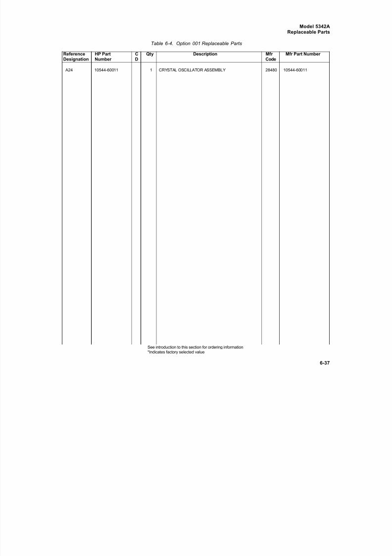
8/21/2019 HP5432 Microwave Frequency Counter
http://slidepdf.com/reader/full/hp5432-microwave-frequency-counter 141/364
Model 5342AReplaceable Parts
Table 6-4. Option 001 Replaceable Parts
Reference HP Part C Qty Description Mfr Mfr Part Number Designation Number D Code
A24 10544-60011 1 CRYSTAL OSCILLATOR ASSEMBLY 28480 10544-60011
See introduction to this section for ordering information*Indicates factory selected value
6-37

8/21/2019 HP5432 Microwave Frequency Counter
http://slidepdf.com/reader/full/hp5432-microwave-frequency-counter 142/364
Model 5342AReplaceable Parts
Table 6-5. Option 002 Replaceable Parts
Reference HP Part C Qty Description Mfr Mfr Part Number Designation Number D Code
A16 05302-60038 9 1 AMPLITUDE MEASUREMENT ASSEMBLY 28480 05342-60038(SERIES 1812)
A16C1 0160-3879 7 10 CAPACITOR=FXD .01UF +-20% 100VDC CER 28480 0160-3879 A16C2 0160-3879 7 CAPACITOR=FXD .01UF +-20% 100VDC CER A16C3 0160-3879 7 CAPACITOR=FXD .01UF +-20% 100VDC CER A16C4 0160-3879 7 CAPACITOR=FXD .01UF +-20% 100VDC CER A16C5 0160-3879 7 CAPACITOR=FXD .01UF +-20% 100VDC CER A16C6 0160-3879 7 CAPACITOR=FXD .01UF +-20% 100VDC CER A16C7 0160-3879 7 CAPACITOR=FXD .01UF +-20% 100VDC CER A16C8 0160-0490 4 3 CAPACITOR=FXD 68UF +-10% 6 VDC TA A16C9 0160-0579 5 15 CAPACITOR=FXD .1UF +-20% 50VDC CER A16C10 0160-0576 5 CAPACITOR=FXD .1UF +-20% 50VDC CER A16C11 0160-4401 3 1 CAPACITOR=FXD .01UF +-10% 100VDC POLYP A16C12 0160-0576 5 CAPACITOR=FXD .1UF +-20% 50VDC CER 28480 0160-0576 A16C13 0180-0491 5 3 CAPACITOR=FXD 10UF +-20% 25VDC TA 28480 0180-0491 A16C14 0160-0576 5 CAPACITOR=FXD .1UF +-20% 50VDC CER 28480 0160-0576 A16C15 0160-0576 5 CAPACITOR=FXD .1UF +-20% 50VDC CER 28480 0160-0576 A16C16 0160-0576 5 CAPACITOR=FXD .1UF +-20% 50VDC CER 28480 0160-0576 A16C17 0180-0491 5 CAPACITOR=FXD .10UF +-20% 25VDC TA 28480 0180-0491 A16C18 0160-0576 5 CAPACITOR=FXD .1UF +-20% 50VDC CER 28480 0160-0576 A16C19 0180-0491 5 CAPACITOR=FXD 10UF +-20% 25VDC TA 28480 0180-0491
A16C20 0160-3879 7 CAPACITOR=FXD .01UF +-20% 100VDC CER 28480 0160-3879 A16C21 0140-0159 8 1 CAPACITOR=FXD 3000PF +-2% 300VDC MICA 72136 DM19F302G0300WV1CR A16C22 0160-2205 1 1 CAPACITOR=FXD 120PF +-5% 300VDC MICA 28480 0160-2205 A16C23 0160-3704 7 1 CAPACITOR=FXD .015UF +-5% 50VDC 28480 0160-3704 A16C24 0140-0190 7 1 CAPACITOR=FXD 39PF +-5% 300VDC MICA 72136 DM56390J0300WV1CR A16C25 0170-0040 9 2 CAPACITOR=FXD .47UF +-10% 200VDC POLYE 56269 292P47392 A16C26 0170-0040 9 CAPACITOR=FXD .47UF +-10% 200VDC POLYE 56269 292P47392 A16C27 0160-0576 5 CAPACITOR=FXD .1UF +-20% 50VDC CER 28480 0160-0576 A16C28 0160-0576 4 CAPACITOR=FXD .68UF +-10% 6VDC TA 90201 T0C686K006WLF A16C29 0160-0579 5 CAPACITOR=FXD .1UF +-20% 50VDC CER 28480 0160-0576 A16C30 0160-0128 5 CAPACITOR=FXD .1UF +-20% 50VDC CER 28480 0160-0576 A16C31 0160-3879 4 CAPACITOR=FXD 66UF +-10% 6VDC TA 90201 TOC686K006WLF A16C32 0160-0576 5 CAPACITOR=FXD .1UF +-20% 50VDC CER 28480 0160-0576 A16C33 0160-0576 5 CAPACITOR=FXD .1UF +-20% 50VDC CER 28480 0160-0576 A16C34 0160-3879 5 CAPACITOR=FXD .1UF +-20% 50VDC CER 28480 0160-0576 A16C35 0160-0128 3 1 CAPACITOR=FXD 2.2UF +-20% 50VDC CER 28480 0160-0128 A16C36 0160-3879 7 CAPACITOR=FXD .01UF +-20% 100VDC CER 28480 0160-3879 A16C37 0160-0576 5 CAPACITOR=FXD .1UF +-20% 50VDC CER 28480 0160-0576 A16C38 0160-0576 5 CAPACITOR=FXD .1UF +-20% 50VDC CER 28480 0160-0576
A16C39 0160-3879 7 CAPACITOR=FXD .01UF +-20% 100VDC CER 28480 0160-3879 A16CR1 1901-0040 1 3 DIODE=SWITCHING 30V 50MA 2NS DO-35 28480 1901-0040 A16CR2 1901-0040 1 DIODE=SWITCHING 30V 50MA 2NS DO-35 28480 1901-0040 A16CR3 1901-0731 7 1 DIODE=PWR RECT 400V 1A 28480 1901-0731 A16CR4 1902-0064 1 1 DIODE=ZNR 7.5V 5% DO=7 PO=4W TC=+.05% 28480 1902-0064 A16CR5 1901-0040 1 DIODE=SWITCHING 30V 50MA 2NS DO-35 28480 1901-0040 A16K1 0490-0617 4 1 RELAY=REED 1C 250MA 28VDC 5VDC-COIL 28480 0190-0617 A16L1 9140-0131 5 2 COIL-MLO 10MH 5% Q=60 .240X.74LG.NOM 28480 9140-0131 A16L2 9140-0131 5 COIL-MLO 10MH 5% Q=60 .240X.74LG.NOM 28480 9140-0131 A16Q1 1853-0058 8 5 TRANSISTOR PNP 81 PD=300MN FT=200MHZ 07263 832248 A16Q2 1853-0058 8 TRANSISTOR PNP 81 PD=300MN FT=200MHZ 07263 832248 A16Q3 1853-0058 8 TRANSISTOR PNP 81 PD=300MN FT=200MHZ 07263 832248 A16Q4 1854-0246 8 4 TRANSISTOR PNP 81 PD=350MN FT=250MHZ 04713 8PB 233 A16Q5 1854-0246 8 TRANSISTOR PNP 81 PD=350MN FT=250MHZ 04713 8PB 233 A16Q6 1854-0246 8 TRANSISTOR NPN 81 PD=350MN FT=250MHZ 04713 8PB 233 A16Q7 1853-0058 8 TRANSISTOR PNP 81 PD=300MN FT=200MHZ 07263 832248 A16Q8 1854-0246 8 TRANSISTOR NPN 81 PD=350MN FT=250MHZ 04713 8PS 233 A16Q9 1853-0058 8 TRANSISTOR PNP 81 PD=300MN FT=200MHZ 07263 332248 A16Q10 1854-0691 7 3 TRANSISTOR NPN 81 TO-92 PD=350 28480 1850-0691 A16Q11 1854-0691 7 TRANSISTOR NPN 81 TO=92 PD=350MN 28480 1854-0691 A16Q12 1854-0691 7 TRANSISTOR NPN 81 TO=92 PD=350MN 28480 1854-0691 A16Q13 1850-0071 7 1 TRANSISTOR NPN 81 PD=300MW FT=200MHZ 28480 1854-0071 A16R1 0698-7260 7 9 RESISTOR 10K 1% .05W F TC=0=-100 24544 C3-1/6=TO=1002=G A16R2 0698-7260 7 RESISTOR 10K 1% .05W F TC=0=-100 24544 C3-1/6=TO=1002=G A16R3 0757-0399 5 2 RESISTOR 82.5 1% .125W F TC=0=-100 24546 C4-1/8=TO=82R5=F A16R4 0698-7260 7 RESISTOR 10K 1% .05W F TC=0=-100 24546 C3-1/6=TO=1002=G A16R5 0698-7260 7 RESISTOR 10K 1% .05W F TC=0=-100 24546 C3-1/6=TO=1002=G A16R6 0698-7260 7 RESISTOR 10K 1% .05W F TC=0=-100 24546 C3-1/6=TO=1002=G A16R7 0698-7234 5 1 RESISTOR 825 1% .05W F TC=0=-100 24546 C3-1/6=TO=4258=G A16R8 0698-4243 6 2 RESISTOR 1.96K 1% .05W F TC=0=-100 24546 C3-1/6=TO=1961-G A16R9 0698-7252 7 1 RESISTOR 4.64K 1% .05W F TC=0=-100 24546 C3-1/8=TO=8641-G A16R10 0757-0407 6 1 RESISTOR 200 1% .125W F TC=0+=100 24546 C4-1/8=TO=201=F
See introduction to this section for ordering information*Indicates factory selected value
6-38

8/21/2019 HP5432 Microwave Frequency Counter
http://slidepdf.com/reader/full/hp5432-microwave-frequency-counter 143/364
Model 5342AReplaceable Parts
Table 6-5. Option 002 Replaceable Parts)
Reference HP Part C Qty Description Mfr Mfr Part Number Designation Number D Code A16R11 0698-7243 6 RESISTOR 1.96K 1% .05 F TC=0+-100 24546 C3-3/8-T0-1961-G A16R12 0698-7236 7 2 RESISTOR 1K 1% .05W F TC=0+-100 24546 C3-3/8-T0-1001-G A16R13 0757-0418 9 1 RESISTOR 619 1% .125W F TC+-100 24546 C3-3/8-T0-619R-F A16R14 0698-7260 7 RESISTOR 10K 1% .5W F TC=0+-100 24546 C3-3/8-T0-1002-G
A16R15 0757-0399 5 RESISTOR 82.5 1% .125W F TC=0+-100 24546 C3-3/8-T0-8245-F A16R16 0698-7236 7 RESISTOR 1K 1% .05W F TC=0+-100 24546 C3-3/8-T0-1001-G A16R17 0698-7260 7 RESISTOR 10K 1% .05W F TC=0+-100 24546 C3-3/8-T0-1002-G A16R18 0698-7260 7 RESISTOR 10K 1% .05W F TC=0+-100 24546 C3-3/8-T0-1002-G A16R19 0698-7260 7 RESISTOR 10K 1% .05W F TC=0+-100 24546 C3-3/8-T0-1002-G A16R20 0698-7332 4 1 RESISTOR 1K 1% .125W F TC=0+-100 28480 0698-7332 A16R21 2100-3122 9 1 RESISTOR-TRMR 100 10% C SIDE-ADJ 17 TRN 02111 43P101 A16R22 0757-0424 7 1 RESISTOR 1.1K 1% .125W F TC=0+-100 24546 C4-1/8-T0-1101-F A16R23 0757-0438 3 1 RESISTOR 5.11K 1% .125W F TC=0+-100 24546 C4-1/8-T0-5111-F A16R24 0698-3154 0 1 RESISTOR 4.22K 1% .125W F TC=0+-100 24546 C4-1/8-T0-4221-F A16R25 0698-3150 6 1 RESISTOR 2.37K 1% .125W F TC=+-100 24546 C4-1/8-T0-2371-F A16R26 2100-3103 6 1 RESISTOR-TRMR 10K 10% C SIDE+ADJ 17-TRN 02111 43P103 A16R27 0698-0084 9 1 RESISTOR 2.15K 1% .125W F T=0+-100 24546 C4-1/8-T0-7501-F A16R28 0757-0260 3 1 RESISTOR 1K 1% .125W F TC=+-100 24546 C4-1/8-T0-7501-F A16R29 2100-3095 5 1 RESISTOR-TRMR 200 10% C SIDE-ADJ 17-TRN 02111 43P201 A16R30 0757-0422 5 1 RESISTOR 909 1% .125W F TC=0+-100 24546 C4-1/8-T0-9098 A16R31 0757-0440 7 2 RESISTOR 7.5K 1% .125W F TC=0+-100 24546 C4-1/8-T0-7501-F A16R32 0757-0440 7 RESISTOR 7.5K 1% .125W F TC=0+-100 24546 C4-1/8-T0-7501-F A16R33 0757-0421 4 3 RESISTOR 825 1% .125W F TC=0+-100 24546 C4-1/8-T0-8258-F
A16R34 0698-6619 8 1 RESISTOR 15K .1% .125W F TC=0+-25 28480 0698-6362 A16R35 0757-0421 4 RESISTOR 825 1% .125W F TC=0+-100 24546 C4-1/8-T0-8258-F A16R36 0698-6362 8 1 RESISTOR 1K .1% .125W F TC=0+-25 28480 0698-6362 A16R37 0757-0421 4 RESISTOR 825 1% .125W F TC=0+-100 24546 C4-1/8-T0-8258-F A16R38 0698-3155 1 1 RESISTOR 4.64K 1% .125W F TC=0+-100 24546 C4-1/8-T0-4641-F A16TP1 0360-0535 0 11 TERMINAL TEST POINT PCB 00000 ORDER BY DESCRIPTION A16TP2 0360-0535 0 TERMINAL TEST POINT PCB 00000 ORDER BY DESCRIPTION A16TP3 0360-0535 0 TERMINAL TEST POINT PCB 00000 ORDER BY DESCRIPTION A16TP4 0360-0535 0 TERMINAL TEST POINT PCB 00000 ORDER BY DESCRIPTION A16TP5 0360-0535 0 TERMINAL TEST POINT PCB 00000 ORDER BY DESCRIPTION A16TP6 0360-0535 0 TERMINAL TEST POINT PCB 00000 ORDER BY DESCRIPTION A16TP7 0360-0535 0 TERMINAL TEST POINT PCB 00000 ORDER BY DESCRIPTION A16TP8 0360-0535 0 TERMINAL TEST POINT PCB 00000 ORDER BY DESCRIPTION A16TP9 0360-0535 0 TERMINAL TEST POINT PCB 00000 ORDER BY DESCRIPTION A16TP10 0360-0535 0 TERMINAL TEST POINT PCB 00000 ORDER BY DESCRIPTION A16TP11 0360-0535 0 TERMINAL TEST POINT PCB 00000 ORDER BY DESCRIPTION A1601 1820-1199 1 1 IC INV TTL LS HEX 1-INP 01295 SN74L525BN A1602 1820-1144 6 1 IC GATE TTL LS NOR QUAD 2-INP 01295 SN74L525BN A1603 05342-80005 2 2 PROW (WATCHED PAIR) 28480 05342-60005
A1604 1818-0468 0 1 IC NMOS B192-BIT ROM 45C-NS 3-S 18324 B2S2708 PROGRAMMED A1605 1820-1195 7 1 IC FF TTL LS D-TYPE POS-EDGE-TRIG COM 01295 SN74LS175N A1606 1820-1439 2 2 IC MUXR/DATA-SEL TTL LS 2-TO-1-LINE 01295 SN74L36BN A1607 1820-1439 2 IC MUXR/DATA-SEL TTL LS 2-TO-1-LINE 01295 SN74L36BN A1608 1820-1995 5 1 IC 7550 CONVB AD-DIP-C 24355 AD7550BD A1609 1820-1207 2 1 IC GATE TTL LS NAND 8-INP 01295 SN4L830N A16010 1820-1442 7 1 IC CNTR TTL LS DECD ASNCHRO 01295 SN4L8290N A16011 1826-0316 4 1 IC REF AMPL TO-5 27014 LH0070-14 A16012 1826-0471 2 1 IC OP AMP TO-94 06665 OP-07CJ A16013 1826-0480 3 2 IC SWITCH 16-DIP-F 27014 LF13333N A16014 1820-0477 6 1 IC OP AMP 8-DIP-P 27014 LM301AN A16015 1820-0224 1 1 IC OP AMP TO-99 27014 LH0002CH A16016 1826-0371 1 1 IC OP AMP TO-99 27014 LF2564 A16017 1826-0480 3 IC SWITCH 16-DIP-P 27014 LF13333N A16018 1826-0472 3 1 IC OP AMP TO-99 27014 LH0D44ACH
A16 MISCELLANEIOUS PARTS0360-0065 1 2 TERMINAL-STUD FKD-TUR SWGFRM-MTG 28480 0360-00651200-0424 9 1 SOCKET-IC BLK 14 CONTACT 23884 CSA2900-14B1200-0525 1 1 SOCKET-IC 20-CONT DBL STRP DIP-SLDR 28480 1200-0525
1200-0552 4 1 SOCKET-IC 40-CONT DIP-BLDR 28480 1200-05521200-0565 9 1 SOCKET-IC 24-CONT DIP-BLDR 28480 1200-05655000-9043 6 1 PINIP.C. BOARD EXTRACTOR 28480 5000-90435040-6552 3 1 EXTRACTOR,ORANGE 28480 5040-685205342-60122 2 1 KIT,WIRES 28480 05342-601220890-0706 0 1 TUBING-KS .093WD/.048-RCVD .02 WALL 28480 0890-07060890-0983 5 1 TUBING-KS .125WD/.062-RCVD .02 WALL 28480 0890-09832200-0155 4 2 SCREW-MACH 4.40 1-IN-LG PAN-HD-POZI 00000 ORDER BY DESCRIPTION2190-0005 0 2 WASHER-LK EXT T NO.4 .116-IN-ID 28480 2190-00050360-0042 4 1 TERMINAL-SLDR LUG PL-MTG FOR-#6-SCR 28480 0360-00421400-0249 0 7 CABLE TIE .062-.625-DEA .091-WD NYL 28480 1400-0249
See introduction to this section for ordering information*Indicates factory selected value
6-39

8/21/2019 HP5432 Microwave Frequency Counter
http://slidepdf.com/reader/full/hp5432-microwave-frequency-counter 144/364
Model 5342AReplaceable Parts
Table 6-5. Option 002 Replaceable Parts)
Reference HP Part C Qty Description Mfr Mfr Part Number
Designation Number D Code
A27 05342-00027 6 1 LOW FREQUENCY AMPLITUDE MODULE 28480 05342-60027
A27C1 0160-3879 7 5 CAPACITOR - FXD .01UF +-20% 1000 VDC CER 28480 0160-3879 A27C3 0160-3879 7 CAPACITOR - FXD .01UF +- 20% 100 VDC CER 28480 0160-0579 A27C4 0160-0576 5 1 CAPACITOR - FXD .1UF +- 20% 50 VDC CER 28480 0160-0576 A27C4 0160-3879 7 CAPACITOR - FXD .01UF +-20% 100 VDC CER 28480 0160-3879 A27C5 0160-3879 7 CAPACITOR - FXD .01UF +- 20% 100 VDC CER 28480 0160-3879
A27C6 0160-3879 7 CAPACITOR - FXD .01UF +- 20% 100 VDC CER 28480 0160-3879 A27C7 0160-4082 6 3 CAPACITOR - FXDT THRU 1000PT +- 20% 200 VDC CER 28480 0160-4082 A27C8 0160-4082 6 CAPACITOR - FXDT THRU 1000PT +- 20% 200 VDC CER 28480 0160-4082 A27C9 0160-4082 6 CAPACITOR - FXDT THRU 1000PT +- 20% 200 VDC CER 28480 0160-4082 A27C10 0160-3926 5 1 CAPACITOR - FXDT THRU 1000PT +- 20% 200 VDC CER 28480 0160-3926
A27CR1 1901-0639 4 2 DIODE - PIN 110V 28480 5082-3080 A27CR2 1901-0639 4 DIODE - PIN 110V 28480 5082-3082 A27CR3/CR4 1906-0208 3 2 DIODE SCHOTTKY 28480 1906-0206
(MATCHED PAIR)
A27J1 1250-0901 2 2 CONNECTOR - RF SMB M SGL - MOLE - FR 50 - OHM 28480 1250-0901
A27J2 1250-0901 2 CONNECTOR - RF SMB M SGL - MOLE - FR 50 - OHM 28480 1250-0901
A27R1 0757-0402 9 1 RESISTOR 10 K 1% .125W F TC=0+-100 24546 C4-1/8-TO-1002-F A27R2 0757-0418 9 3 RESISTOR 619 1% .125W F TC=0+-100 24546 C4-1/8-TO-619R-F A27R3 0757-0418 9 RESISTOR 619 1% .125W F TC=0+-100 24546 C4-1/8-TO-619R-F A27R4 0757-0418 9 RESISTOR 619 1% .125W F TC=0+-100 24546 C4-1/8-TO-619R-F A27R5 0757-0401 0 2 RESISTOR 100 1% .125W F TC=0+-100 24546 C4-1/8-TO-101-F
A27R6* 0698-7202 7 1 RESISTOR 38.3 1% .05W F TC=0+-100 24546 C3-1/8-TO-38R3-G A27R7 0757-0401 0 RESISTOR 100 1% .125W F TC=0+-100 24546 C3-1/8-TO-101-F A27R8 0698-3435 0 1 RESISTOR 38.3 1% .125W F TC=0+-100 24546 C3-1/8-TO-10R3-F A27R9 2100-3053 5 1 RESISTOR TMR 20 20% C SIDE - ADJ 17 - TRN 02111 43P200 A27R10 2100-3095 5 1 RESISTOR TMR 200 10% C SIDE - ADJ 17 - TRN 02111 43P201
05342-00015 4 1 COVER 28480 05342-0001505342-20110 4 1 HOUSING 28480 05342-20110
U2 05342-80005 2 WF AMP ASSY 28480 05342-8005
W1 8120-2660 4 1 CABLE ASSY 28480 8120-2668W2 05342-60119 7 1 CABLE ASSY , LF 50 28480 05342-60119W3 8120-2516 1 1 CABLE ASSY , SEMIRIGID 28480 8120-2316
See introduction to this section for ordering information*Indicates factory selected value
6-40

8/21/2019 HP5432 Microwave Frequency Counter
http://slidepdf.com/reader/full/hp5432-microwave-frequency-counter 145/364
Model 5342AReplaceable Parts
Table 6-6. Option 003 Replaceable Parts
Reference HP Part C Qty Description Mfr Mfr Part Number Designation Number D Code
A16 05342-60037 8 1 EXTENDED DYNAMIC RANGE ASSEMBLY 28480 05342-60037(SERIES 1720)
A16C1 0180-0490 4 2 CAPACITOR-FXD 68UF +-10% 6VDC TA 90201 TDC686KDD06WLF A16C2 0180-0490 4 CAPACITOR-FXD 68UF +-10% 6VDC TA 90201 TDC686KDD06WLF
A16CR1 1901-0040 1 1 DIODE-SWITCHING 30V 50MA 2NS DO-35 28480 1901-0040
A16Q1 1852-0058 8 2 TRANSISTOR PNP SI PD=300MW FT=200MHZ 07263 S32248 A16Q2 1852-0058 8 TRANSISTOR PNP SI PD=300MW FT=200MHZ 07263 S32248 A16Q3 1854-0246 8 1 TRANSISTOR NPN SI PD=350MW FT=250MHZ 04713 SPS 233
A16R1 0757-0407 6 1 RESISTOR 200 1% .125W F TC=0+-100 24546 C4-1/8-TO-201-F A16R2 0757-0442 9 3 RESISTOR 10K 1% .125W F TC=0+-100 24546 C4-1/8-TO-1002-F A16R3 0757-0399 5 2 RESISTOR 82.5 1% .125W F TC=0+-100 24546 C4-1/8-TO-82R5-F A16R4 0757-0418 9 1 RESISTOR 619 1% .125W F TC=0+-100 24546 C4-1/8-TO-619R-F A16R5 0757-0442 9 RESISTOR 10K 1% .125W F TC=0+-100 24546 C4-1/8-TO-1002-F
A16R6 0757-0280 3 1 RESISTOR 1K 1% .125W F TC=0+-100 24546 C4-1/8-TO-1001-F A16R7 0757-0399 5 RESISTOR 82.5 1% .125W F TC=0+-100 24546 C4-1/8-TO-82R5-F A16R8 0698-3155 1 1 RESISTOR 4.64K 1% .125W F TC=0+-100 24546 C4-1/8-TO-4641-F
A16R9 0757-0442 9 RESISTOR 10K 1% .125W F TC=0+-100 24546 C4-1/8-TO-1002-F A16R10 0757-0421 4 1 RESISTOR 825 1% .125W F TC=0+-100 24546 C4-1/8-TO-825R-F
A16TP1 0360-0535 0 2 TERMINAL TEST POINT PCB 00000 ORDER BY DESCRIPTION A16TP2 0360-0535 0 TERMINAL TEST POINT PCB 00000 ORDER BY DESCRIPTION
9 1
A16W1 8120-2516 1 1 CABLE ASSY, SEMIRIGID 28480 8120-2516
A16 MISCELLANEOUS PARTS
0890-0706 0 1 TUBING-MS .093-0/.046-HCVD .02-WALL 28480 0890-070605342-60123 3 1 KIT, WIRES 28480 05342-60123
U2 5088-7038 ATTENUATOR ASSEMBLY 28480 5088-7038
See introduction to this section for ordering information*Indicates factory selected value
6-41

8/21/2019 HP5432 Microwave Frequency Counter
http://slidepdf.com/reader/full/hp5432-microwave-frequency-counter 146/364
Model 5342AReplaceable Parts
Table 6-7. Option 004 Replaceable Parts
Reference HP Part C Qty Description Mfr Mfr Part Number Designation Number D Code
A2 05342-60026 7 1 DISPLAY DRIVER ASSEMBLY (SERIES 1826) 28480 05342-60028 A2C2 0160-3879 7 6 CAPACITOR-FXD .01UF +-20% 100VDC CER 28480 0160-3879 A2C3 0180-0230 0 1 CAPACITOR-FXD 1UF +-20% 50VDC TA 56289 1500105X0050A2 A2C3 0180-0106 9 2 CAPACITOR-FXD 60UF +-20% 6VDC TA 56289 1500606X0006B2 A2C4 0160-3879 7 CAPACITOR-FXD .01UF +-20% 100VDC CER 28480 0160-3879 A2C5 0180-1743 2 1 CAPACITOR .1UF +-10% 35VDC TA 56289 150D104X9035A2 A2C6 0160-3879 7 CAPACITOR-FXD .01UF +-20% 100VDC CER 28480 0160-3879 A2C7 0160-3878 6 2 CAPACITOR-FXD 1000PF +-20% 100VDC CER 28480 0160-3878 A2C8 0160-3879 7 CAPACITOR-FXD .01UF +-20% 100VDC CER 28480 0160-3879 A2C9 0160-3879 7 CAPACITOR-FXD .01UF +-20% 100VDC CER 28480 0160-3879 A2C10 0180-1714 7 1 CAPACITOR-FXD 330UF +-10% 6VDC TA 56289 1500337X900652 A2C12-C15 NOT ASSIGNED A2C11 0160-3879 7 CAPACITOR-FXD .01UF +-20% 100VDC CER 28480 0160-3879 A2C16 0180-0106 9 CAPACITOR-FXD 60UF +-20% 6VDC TA 56289 150D606X000682 A2C17 0160-3878 6 CAPACITOR-FXD 1000PF +-20% 100VDC CER 28480 0160-3878 A2C18 0160-0573 2 2 CAPACITOR-FXD 4700PF +-20% 100VDC CER 28480 0160-0573 A2C19 0160-0573 2 CAPACITOR-FXD 4700PF +-20% 100VDC CER 28480 0160-0573 A2C20 0160-0570 9 1 CAPACITOR-FXD 220PF +-20% 100VDC CER 28480 0160-0570 A2J2 1250-0257 1 1 CONNECTOR-RF 8MB M PC 50-OHM 28480 1250-0257 A2Q1 1854-0560 9 1 TRANSISTOR NPN SI DARL PD-310MW 04713 SP56740 A2R1 0757-0420 3 1 RESISTOR 750 1% .125W F TC-04-100 24546 C4-1/0-T0-751-F A2R2 1810-0125 0 1 NETWORK-RES 8-PIN-SIP .125-PIN-BPCG 28460 1810-0125
A2R3 0683-5105 4 1 RESISTOR 51 5% .25W FC TC*-400/4500 01121 CB3105 A2R4 0683-2205 9 8 RESISTOR 22 5% .25W FC TC*-400/4500 01121 CB2205 A2R5 0683-1015 7 2 RESISTOR 100 5% .25W FC TC*-400/4500 01121 CB1015 A2R8 2100-3607 5 1 RESISTOR-VAR CONTROL CCP 1M 10% LIN (Not supplied 01121 WP4N102P105U2
with 05342-60028, must be ordered separately)
A2R6 0683-2205 9 RESISTOR 22 5% .25W FC TC*-400/4500 01121 CB2205 A2R7 0683-1025 9 1 RESISTOR 1K 5% .25W FC TC*-400/4600 01121 CB1025 A2R6 0683-2205 9 RESISTOR 22 5% .25W FC TC*-400/4500 01121 CB2205 A2R10 0683-4725 2 11 RESISTOR 4.7K 5% .25W FC TC*-400/4700 01121 CB4725 A2R11 0683-2205 9 RESISTOR 22 5% .25W FC TC*-400/4500 01121 CB2205 A2R12 0683-4725 2 RESISTOR 4.7K 5% .25W FC TC*-400/4700 01121 CB4725 A2R13 0683-2205 9 RESISTOR 22 5% .25W FC TC*-400/4500 01121 CB2205 A2R14 0683-2205 9 RESISTOR 22 5% .25W FC TC*-400/4500 01121 CB2205 A2R15 0683-2205 9 RESISTOR 22 5% .25W FC TC*-400/4500 01121 CB2205 A2R16 0683-2205 9 RESISTOR 22 5% .25W FC TC*-400/4500 01121 CB2205 A2R17 1810-0164 7 1 NETWORK-RES 9-PIN-SIP .15-PIN-8PCG 28480 1B10-0164 A2R18 0683-4725 2 RESISTOR 4.7K 5% .25W FC TC*-400/4700 01121 CB4725 A2R19 0683-4725 2 RESISTOR 4.7K 5% .25W FC TC*-400/4700 01121 CB4725 A2R20 0683-4725 2 RESISTOR 4.7K 5% .25W FC TC*-400/4700 01121 CB4725
A2R21 0683-4725 2 RESISTOR 4.7K 5% .25W FC TC*-400/4700 01121 CB4725 A2R22 0683-1015 7 RESISTOR 100 5% .25W FC TC*-400/4500 01121 CB1015 A2R23 0683-4785 2 RESISTOR 4.7K 5% .25W FC TC*-400/4700 01121 CB4725 A2R24 0683-4725 2 RESISTOR 4.7K 5% .25W FC TC*-400/4700 01121 CB4725 A2R25 2100-2655 1 2 RESISTOR-TRMR 100K 10% C TOP-ADJ 1-TRN 73138 B2PR100K A2R26 0683-4725 2 RESISTOR 4.7K 5% .25M FC TC*-400/4700 01121 CB4725 A2R27 2100-2655 1 RESISTOR-TRMA 100K 10% C TOP-ADJ 1-TRN 71138 82PR100K A2R28 0683-4725 2 RESISTOR 4.7K 5% .25W FC TC*-400/4700 01121 CB4725 A2R29 0683-1035 1 1 RESISTOR 10K 5% .25W FC TC*-400/4700 01121 CB1035 A2R30 0683-1845 1 2 RESISTOR 180K 5% .25W FC TC*-800-4900 01121 CB1845 A2R31 0683-1845 1 RESISTOR 180K 5% .25W FC TC*-800/4900 01121 CB1845 A2R32 0683-2745 2 2 RESISTOR 270K 5% .25W FC TC*-800/4900 01121 CB2745 A2R33 0683-2745 2 RESISTOR 270K 5% .25W FC TC*-800/4900 01121 CB2745 A2R34 0683-3925 2 1 RESISTOR 3.9K 5% .25W FC TC*-400/4700 01121 CB3925 A2R35 0683-4725 2 RESISTOR 4.7K 5% .25W FC TC*-400/4700 01121 CB4725 A2TF1 1251-0600 0 1 CONNECTOR-SGL CONT PIN 1.14-MM-BSC-S2 SQ 28480 1251-0600 A2U1 1820-0539 1 2 IC BFR TTL NAND QUAD 2-INP 01295 8N7437N A2U2 1820-0468 5 2 IC DCDR TTL BCD-TO-DEC 4-TO-10-LINE 01295 8N7445N A2U3 1820-1443 8 1 IC CNTR TTL LS 8IN ASYNCHRO 01295 8N74L8293N
A2U4 1820-0539 1 IC BFR TTL NAND QUAD 2-INP 01295 8N7437N A2U5 1820-1416 5 1 IC SCHMITT-TRIG TTL LS INV HEX 1-INP 01295 8N74LS14N A2U6 1820-1049 0 1 IC BFR TTL NON-INV HEX 01295 8N74367N A2U7 1820-0468 5 IC DCOR TTL BCD-TO-DEC 4-TO-10-LINE 01295 8N7445N A2U8 1820-1028 5 2 IC-DGTL, 64BIT RAM, TTL 01295 8N7189N A2U9 1820-1144 6 1 IC GATE TTL LS NOR QUAD 2-INP 01295 8N74L802N A2U10 1820-1200 5 1 IC INV TTL LS HEX 01295 SN74LS05N A2U11 1820-1025 5 IC-DGTL, 64BIT RAM, TTL 01295 8N7189N A2U12 1820-1254 9 2 IC BFR TTL NON-INV HEX 1-INP 27014 DM8095N A2U13 1820-1425 6 1 IC SCHMITT-TRIG TTL LS NAND QUAD 2-INP 01295 8N74LS132N A2U14 1820-1194 6 3 IC CNTR TTL LS BIN UP/DOWN SYNCHRO 01295 8N74LS193N A2U15 1820-1216 3 1 IC DCDR TTL LS 3-TO-8-LINE 3-INP 01295 SN74LS138N
See introduction to this section for ordering information*Indicates factory selected value
6-42

8/21/2019 HP5432 Microwave Frequency Counter
http://slidepdf.com/reader/full/hp5432-microwave-frequency-counter 147/364
MODEL 5342AReplaceable Parts
Table 6-7. Option 004 Replaceable Parts (Continued)
Reference HP Part C Qty Description Mfr Mfr Part Number Designation Number D Code
A2U16 1820-1250 9 IC BFR TTL NON-INV HEX 1-INP 27014 DM8095N
A2U17 1820-1426 9 1 IC MUXR/DATA-SEL TTL LS 2-TO-1-LINE QUAD 01295 SN74LS158N A2U18 1820-1112 6 2 IC FF TTL LS D-TYPE POS-EDGE-TRIG 01295 SN74LS74N A2U19 1820-1112 6 IC FF TTL D-TYPE POS-EDGE-TRIG 01295 SN74LS74N A2U20 1820-1194 6 IC CNTR TTL LS BIN UP/DOWN SYNCHRO 01295 SN74LS193N A2U21 1820-1194 6 IC CNTR TTL LS BIN UP/DOWN SYNCHRO 01295 SN74LS193N A2U22 1820-1885 2 1 IC AGTR TTL LS D-TYPE QUAD 27014 DM74LS173N A2U23 1813-0092 * 1 IC DAC-60 CONV 24-DIP-C 86175 DAX80-CCD-V
A2*1 05342-60106 2 1 CABLE ASSY, OUTPUT 28460 05342-60106
A2 MISCELLANEOUS PARTS
0380-0336 1 5 SPACER-RVT-ON .312-IN-LG .152-IN-ID 00000 ORDER BY DESCRIP-TION
1200-0565 9 1 SOCKET-IC 24-CONT DIP-SLDR 28480 1200-05651200-0646 7 1 SOCKET-IC 24-CONT DIP-SLDR 28480 1200-060005342-00124 4 1 KIT, WIRES 28480 05342-60124
See introduction to this section for ordering information*Indicates factory selected value
6-43

8/21/2019 HP5432 Microwave Frequency Counter
http://slidepdf.com/reader/full/hp5432-microwave-frequency-counter 148/364
Model 5342AReplaceable Parts
Table 6-8. Option 001 Replaceable Parts
Reference HP Part C Qty Description Mfr Mfr Part Number Designation Number D Code
A15 05342-60015 2 1 HP-IB ASSEMBLY (SERIES 1720) 28480 05342-60015 A15C1 0160-3879 7 11 CAPACITOR=FxD *01UF +-20% 100VDC CER 28480 0160-3879 A15C2 0160-3879 7 CAPACITOR=FxD *01UF +-20% 100VDC CER 28480 0160-3879 A15C3 0160-3879 7 CAPACITOR=FxD *01UF +-20% 100VDC CER 28480 0160-3879 A15C4 0160-3879 7 CAPACITOR=FxD *01UF +-20% 100VDC CER 28480 0160-3879 A15C5 0160-3879 7 CAPACITOR=FxD *01UF +-20% 100VDC CER 28480 0160-3879 A15C6 0160-3879 7 CAPACITOR=FxD *01UF +-20% 100VDC CER 28480 0160-3879 A15C7 0160-3879 7 CAPACITOR=FxD *01UF +-20% 100VDC CER 28480 0160-3879 A15C8 0160-3879 7 CAPACITOR=FxD *01UF +-20% 100VDC CER 28480 0160-3879 A15C9 0160-0106 9 1 CAPACITOR=FxD *01UF+-20% 6VDC TA 56289 1500606X000682 A15C10 0160-3879 7 CAPACITOR=FxD *01UF +-20% 100VDC CER 28480 0160-3879 A15C12 0130-3879 7 CAPACITOR=FxD *01UF +-20% 100VDC CER 28480 0160-3879 A15C13 0160-3879 7 CAPACITOR=FxD *01UF +-20% 100VDC CER 28480 0160-3879 A15C1 0100-1788 6 1 CHOKE.WIDBAND ZMAXB660 OHM@ 180 MHZ 02114 VK200 20/48
A15R1 0787-0390 0 1 RESISTOR 51.1 1% .125W F TC=0+=100 24548 C4-1/8-T0-5181-F A15R2 1810-0164 7 3 NETWORK-RES 9-PIN-SIP .15-PIN-8PCG 28480 1810-0164 A15R3 1810-0164 7 NETWORK-RES 9-PIN-SIP .15-PIN-8PCG 28480 1810-0164 A15R4 1810-0164 7 NETWORK-RES 9-PIN-SIP .15-PIN-8PCG 28480 1810-0164
0360-0124 3 2 CONNECTOR-8GL CONT PIN .04-IN-6SC-32 RND 28480 0360-01240360-0124 3 CONNECTOR-8GL CONT PIN .04-IN-6SC-32 RND 28480 0360-0124
A15U1 1820-1197 9 2 IC GATE TTL L8 NAND QUAD 2-INP 01295 BN74L800N A15U2 1820-1144 6 4 IC GATE TTL L8 NAND QUAD 2-INP 01295 BN74L802N A15U3 1820-1112 6 8 IC FF TTL L8 D-TYPE PO8-EDGE-TRIG 01295 BN74L874N A15U4 1820-1112 8 IC FF TTL L8 D-TYPE PO8-EDGE-TRIG 01295 BN74L874N A15U5 1820-1144 6 IC GATE TTL L8 NOR QUAD 2-INP 01295 8N74L802N A15U6 1820-1144 6 IC GATE TTL L8 NOR QUAD 2-INP 01295 BN74L802N A15U7 1820-1211 8 1 IC GATE TTL L8 EXCL-DR QUAD 2-INP 01295 BN74L886N A15U8 1820-1144 6 IC GATE TTL L8 NOR QUAD 2-INP 01295 BN74L802N A15U9 1820-1112 8 IC FF TTL L8 D-TYPE POPS-EDGE-TRIG 01295 BN74L874N A15U10 1820-1112 5 IC FF TTL L8 D-TYPE POPS-EDGE-TRIG 01295 BN74L874N A15U11 1820-1210 3 1 IC DCDR TTL L8 3-TO-8 LINE 3-INP 01295 BN74L5138N A15U12 1820-1206 1 1 IC GATE TTL L8 NOR TTL 3-INP 01295 BN74L827N A15U13 1820-1199 1 1 IC INV TTL L8 HEX 1-INP 01295 BN74L804N A15U14 1820-1112 6 IC FF TTL L8 D-TYPE POS-EDGE-TRIG 01295 BN74L874N A15U15 1820-0570 6 1 IC AG7R TTL D-TYPE 4-BIT 01295 BN74173N A15U16 1820-1196 6 1 IC FF TTL L8 D-TYPE POS-EDGE-TRIG COM 01295 BN74L8174N A15U17 1820-1198 6 1 IC GATE TTL L8 NAND QUAD 2-INP 01295 BN74L803N A15U18 1820-1368 6 2 IC DRVR TTL BUS DRVR DEX 1-INP 01295 BN74366N A15U19 1820-1112 8 IC FF TTL L8 D-TYPE POS-EDGE-TRIG 01295 BN74L874N
A15U20 1820-1282 1 2 IC FF TTL L8 J-K BAR POS-EDGE-TRIG 01295 BN74L8109N A15U21 1820-1997 7 3 IC FF TTL L8 D-TYPE POS-EDGE-TRIG PRL-IN 34335 BN74L8374PC A15U22 1820-1659 4 4 IC MISC QUAD 04713 MC3496P A15U23 1816-1154 9 1 ROM 32 X 8 OC 01295 BN748180N PROGRAMMED
1200-0473 8 2 SOCKET-IC 16 CONT DIF DIP-SLDR 28480 1200=0473 A15U24 1820-1997 7 IC FF TTL L8 D-TYPE POS-EDGE-TRIG PRL-IN 34335 BN7465374PC A15U25 1820-1669 4 IC MISC QUAD 04713 MC3446P A15U26 1816-1155 0 1 ROM 32 X 8 OC 01295 BN748100N PROGRAMMED
1200-0473 8 SOCKET-IC 16 CONT DIF DIP-SLDR 28480 1200-0473 A15U27 1820-1997 7 IC FF TTL L8 D-TYPE POS-EDGE-TRIG PRL-IN 38335 BN74L8374PC A15U28 1820-1689 4 IC MISC QUAD 04713 MC3446P A15U29 1820-1282 3 IC FF TTL L8 J-K BAR POS-EDGE-TRIG 01295 BN74L8109N A15U30 1820-1368 6 IC DRVR TTL BUS DRVR DEX 1-INP 01295 BN74366N A15U31 1820-1689 4 IC MISC QUAD 04713 MC3446P A15U32 1820-1202 7 1 IC GATE TTL L8 NAND TRL 3-INP 01295 BN74L810N A15U33 1820-0904 4 1 IC COMPUTER TTL L MAGTD 5-BIT 07261 93L24PC A15U34 1820-1112 8 IC FF TTL L8 D-TYPE POS-EDGE-TRIG 01295 BN74L874N A15U35 1820-1112 8 IC FF TTL L8 D-TYPE POS-EDGE-TRIG 01295 BN74L874N A15U36 1820-1197 9 IC GATE TTL L8 NAND QUAD 2-INP 01295 BN74L800N
5000-9043 6 1 PIN, P.C. BOARD EXTRACTOR 28480 5000-90435040-6852 3 1 EXTRACTOR, ORANGE 28480 5040-6852
A29 05342-60029 6 1 HP-1B INPUT ASSEMBLY (SERIES 1720) 28480 05342-60029 A29J1 1251-3283 1 1 CONNECTOR 24-PIN F MICRORIBBON 28480 1251-3283 A29J2 1200-0485 2 1 0KT=IC, 14 PIN, PC M7G1 RT AGLE CONT 28480 1200-0485 A29S1 3101-1973 7 1 SWITCH--8L 7-1A-N8 DIF-SLIDE-ASSY *1A 28480 3101-1973 A29W5 0120-1966 3 1 CABLE ASSY 26AWG 24-CNDCT 28480 8120-1966
A29 MISCELLANEOUS PARTS0380-0644 4 2 STANDOFF-METRIC SHORT STUD MOUNTS FOR 28480 0380-06441830-1098 4 2 CLEVIS 0.070-IN W SLTS 0.454-IN PIN CTR 00000 ORDER BY DESCRIPTION2190-0034 5 2 WASHER-LK HLCL NO. 10, 194-IN-ID 28480 2190-003405342-00017 8 1 PLATE, PATCH 28480 05342-00017
See introduction to this section for ordering information*Indicates factory selected value
6-44

8/21/2019 HP5432 Microwave Frequency Counter
http://slidepdf.com/reader/full/hp5432-microwave-frequency-counter 149/364
Model 5342AReplaceable Parts
Table 6-9. Manufacturers Code List
MFG NO. MANUFACTURER NAME ADDRESS ZIP CODE
00000 Any Satisfactory Supplier
0046G Norelco North Amer Philips Ltg Corp Los Angeles, CA 90021
01121 Allen-Bradley Co Milwaukee, WI 53204
01295 Texas Instr Inc Semiconductor Cmpnt Div Dallas, TX 75222
01926 RCA Corp Solid State Div Somerville, NJ 0887602111 Spectrol Electronics Corp City of Ind, CA 91745
02114 Ferroxcube Corp Saugerties, NY 12477
03508 GE Co Semiconductor Prod Dept Syracuse, NY 13201
03888 KDI Pyrofilm Corp Whippany, NJ 07981
04713 Motorola Semiconductor Products Phoenix, AZ 85062
06665 Precision Monolithic Inc Santa Clara, CA 95050
07263 Fairchild Semiconductor Div Mountain View, CA 94042
09023 Cornell-Dubilier Elek Div Fed Pac Sanford, CA 27330
16546 U.S. Capacitor Corp Burbank, CA 91504
18324 Signetics Corp Sunnyva le , CA 94086
19701 Mepco/Electra Corp Mineral Wells , TX 76067
2388A No M/F Description for this Mfg No.24355 Analog Devices Inc Norwood, MA 02062
24546 Corning Glass Works (Bradford) Bradford, PA 16701
25403 Amperex Elek Corp Semicon & MC Div Slatersville, RI 02876
27014 National Semiconductor Corp Santa Clara, CA 95051
28480 Hewlett-Packard Co Corporate HQ Palo Alto, CA 94304
30983 Mepco/Electra Corp San Diego, CA 92121
34335 Advanced Micro Devices Inc Sunnyva!e, CA 94086
50088 Mostek Corp Carrollton, TX 75006
56289 Sprague Electric Co North Adams, MA 01247
72136 Electro Motive Corp Sub IEC Wil limantic, CT 06226
73138 Beckman Instruments Inc Helipot Div Fullerton, CA 92634
75915 Littelfuse Inc Des Plaines, IL 60016
8E175 Burr Brown Co Huntsville, AL 35801
90201 Mallory Capacitor Co Indianapolis, IN 46206
6-45

8/21/2019 HP5432 Microwave Frequency Counter
http://slidepdf.com/reader/full/hp5432-microwave-frequency-counter 150/364
Model 5342A
Manual Changes
SECTION VIIMANUAL CHANGES
7-1. INTRODUCTION
7-2. This section contains information necessary to adapt this manual to apply to olderinstruments.
7-3. MANUAL CHANGES
7-4. This manual applies directly to Model 5342A Microwave Frequency Counters with serialnumber prefix 1840A.
7-5. As engineering changes are made, newer instruments may have serial prefix numbershigher than those listed on the title page of this manual. The manuals for these instruments will besupplied with MANUAL CHANGES sheets containing the required information.
MANUAL DESCRIPTION
INSTRUMENT: 5342A Microwave Freq. Counter
Operating and Service Manual
SERIAL PREFIX: 1840A
DATE PRINTED: FEB. 1979
HP PART NO: 05342-90013
MICROFICHE NO: 05342-90014
CHANGE DATE: July 19, 1979
(This change supersedes all earlier dated
changes)
Make all changes listed as ERRATA.
Check the following table for yourinstrument’s serial prefix or serial number
and make listed change(s) to manual.
IF YOUR INSTRUMENT MAKE THE IF YOUR INSTRUMENT MAKE THE
HAS SERIAL PREFIX FOLLOWING CHANGES HAS SERIAL PREFIX FOLLOWING CHANGES
OR SERIAL NUMBER TO YOUR MANUAL OR SERIAL NUMBER TO YOUR MANUAL
1904A 1
1916A 1, 2
NEW OR REVISED ITEM
ERRATA
Page 1-5, Table 1-4, Recommended Test Equipment:
Add Frequency Counter capable of frequency measurements up to at least 350 MHz for troubleshooting A8, A9,
and A10 Main Loop Synthesizer. The HP Model 5345A Electronic Counter is recommended. Use Channel A inputset for 50Q input impedance.
/8440-8643-8647/9081-8626/E/
7-1

8/21/2019 HP5432 Microwave Frequency Counter
http://slidepdf.com/reader/full/hp5432-microwave-frequency-counter 151/364
Model 5342AManual Changes
ERRATA (Cont’d)
Page 8-113, Table 8-15, Main Loop Synthesizer Troubleshooting:
Change text of first paragraph in step 2 to the following:
2. To test if the A8 Main VCO is operating properly, put the 5342A in MANUAL mode, 500 MHz - 18 GHz range,and set the MANUAL center frequency to the values in the following table. Connect a coax cable, with
5345A measurement indicates the correct MAIN OSC frequency for each of the MANUAL center fre-quencies selected.
Page 6-32, Table 6-3, A24 (05341-60047) Replaceable Parts:Add A24 MISCELLANEOUS; 0380-0044; CD=6; SPACER 0.25 INCH; 28480; 0380-0044.
Page 8-179, Figure 8-39, A16 (OPTION 002) Schematic Diagram:Change color of cable to J7 pins 2 and 13 from ORN to RED.
Page 6-7, Table 6-3, A2 Replaceable Parts:
Change “Reference Designation” for A2C6 (part number 0180-0106) from “A2C6” to A2C1.
Page 6-42, Table 6-7:Change “Reference Designation” for A2C3 (part number 0180-0106) from “A2C3” to A2C1.
Add A2C12, C14, C15; 0180-0230; CD=0; CAPACITOR-FXD 1UF ±20%, 50VDC TA; 56289; 150D105X0050A2.Add A2C13; 0160-3879; CD=6; CAPACITOR-FXD 0.01 UF ±20% 100VDC CER; 28480; 0160-3879.
Page 8-187, Figure 8-43, P/O A22 Motherboard Schematic:Change reference designation for “OVEN TRANSFORMER” from “T4” to T1.
Add troubleshooting information in attached Table 1 on aprons of schematic diagrams as specified in the table.
Page 6-41, Table 6-6, Option 003 Miscellaneous Replaceable Parts:Add 5000-9043; CD=6; PIN: P.C. BOARD EXTRACTOR; 28480; 5000-9043.Add 5040-6852; CD=3; EXTRACTOR, ORANGE; 28480; 5040-6852.
Page 8-149, Figure 8-24, A2 REFERENCE DESIGNATIONS table:Change “C19” under “Deleted:” to C9.
Page 1-2, Table 1-1, Specifications:
Change 10544A Short Term Stability to <1 X 10 -10 for 1 second average time.
7 - 2
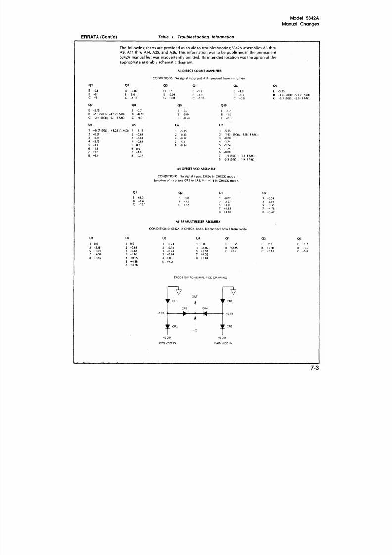
8/21/2019 HP5432 Microwave Frequency Counter
http://slidepdf.com/reader/full/hp5432-microwave-frequency-counter 152/364
Model 5342A
Manual Changes
ERRATA (Cont’d) Table 1. Troubleshooting Information
7-3

8/21/2019 HP5432 Microwave Frequency Counter
http://slidepdf.com/reader/full/hp5432-microwave-frequency-counter 153/364
Model 5342AManual Changes
ERRATA (Cont’d) Table 1. Troubleshooting Information (Continued)
7-4

8/21/2019 HP5432 Microwave Frequency Counter
http://slidepdf.com/reader/full/hp5432-microwave-frequency-counter 154/364
Model 5342A
Manual Changes
ERRATA (Cont’d) Table 1. Troubleshooting Information (Continued)
7-5

8/21/2019 HP5432 Microwave Frequency Counter
http://slidepdf.com/reader/full/hp5432-microwave-frequency-counter 155/364
Model 5342AManual Changes
ERRATA (Cont'd) Table 1. Troubleshooting Information (Continued)
7 - 6

8/21/2019 HP5432 Microwave Frequency Counter
http://slidepdf.com/reader/full/hp5432-microwave-frequency-counter 156/364
Model 5342A
Manual Changes
CHANGE 1 (1904A)
Pages 6-33 and 6-34, Table 6-3, A25 (05342-60025) Replaceable Parts:Change A25 from SERIES 1804 to SERIES 1904.Delete A25C32 capacitor HP Part No. 0160-4082.Delete A25CR3 and CR4 diodes HP Part No. 1901-0040.Delete A25Q3 transistor HP Part No. 1854-0071.Delete A25R35 resistor HP Part No. 0698-7241.Delete A25R37 resistor HP Part No. 0698-7259.
Delete A25R38 resistor HP Part No. 0698-7253.NOTE: The above parts serve no electrical function on circuit board assembly A25.
Page 8-191, Figure 8-45, A25 Schematic Diagram:Change series number at top of diagram from 1804 to 1904.
Delete A25C32, CR3, CR4, Q3, R35, R37, and R38.
Make appropriate changes in REFERENCE DESIGNATIONS table and TABLE OF ACTIVE ELEMENTS.
Page 6-36, Table 6-3, Miscellaneous Replaceable Parts:Add 1400-0985; CD=1; CLAMP, RIBBON CABLE; 28480; 1400-0985.
CHANGE 2 (1916A)
Page 6-5, Table 6-3, Al (05342-60001] Replaceable Parts:Change Al from SERIES 1720 to SERIES 1916.
Change A1DS1 thru A1DS8 to 1990-0670 in HP Part Number and Mfr Part Number columns.Change CD column from “7” to “0”.
Page 8-149, Figure 8-24, Al Schematic Diagram:Change SERIES 1720 at top of Al diagram of Display Assembly to SERIES 1916.
7-6. OLDER INSTRUMENTS
7-7. To adapt this manual to older instruments having a serial prefix lower than 1840A, performthe backdating that applies to your instruments serial prefix as listed in Table 7-I below.
Table 7-1. Manual BackdatingIf Instrument has Serial Prefix Make the Following Changes to Manual
1828 11812 1,21808 1,2,31804 1,2,3,4
1 7 2 0 1,2,3,4,5
CHANGE 1Page 6-7, Table 6-3, A2 Replaceable Parts:
Change A2 series number from 1828 to 1804.Delete “A2C20: 0160-0570: CAPACITOR-FXD 220PF 20% 100VDC CER: 28480:0160-0570”.Change A2R22’ from 0683-1015 1 to “0683-2015; RESISTOR-FXD 200 5%’ .25 FC TC=-400/+600;
0160G; CB2015”,
Change A2U13 from 1820-1425 to “1820-1197; IC GATE TTL LS NAND QUAD 2-INP; 0169H;SN74LS00N”.
Change A2U22 from 1820-1885 to “1820-0574; IC FF TTL D-TYPE COM CLEAR QUAD; 0340F;DM8551N”.
Page 8-149, Figure 8-24, A1 and A2 Schematic Diagram:Change A2 series number from “1828” to “1804”.Change the value of resistor A2R22 from 100 to 200 ohms.Delete capacitor C20 from A2U8, pin 3.
7-7

8/21/2019 HP5432 Microwave Frequency Counter
http://slidepdf.com/reader/full/hp5432-microwave-frequency-counter 157/364
Model 5342AManual Changes
CHANGE 2Page 6-23, Table 6-3, A14 Replaceable Parts:
change A14 series number from 1840 to 1812.Change A14U7 part number from 1818-0706 to 1818-0331, Annotate that the older part number
(1818-0331) is obsolete and the new part number (1818-0706) is the recommended replacement,
Page 8-175, Figure 8-37, A14 Schematic Diagram:Change A14 series number from “1840” to “1812”,
CHANGE 3Page 6-23, Table 6-3, A14 Replaceable Parts:
Change A14 series number from 1812 to 1808,Delete “A14C28; 0160-3878; CAPACITOR-FXD 1000PF ±20% I00VDC CER; 28480; 0160-3878”.
Page 8-175, Figure 8-37, A14 Schematic Diagram:Delete A14C28 (1000PF) from U11A, pin 3.Change series number (top of diagram) from “1812” to “1808”,
Page 6-23, Table 6-3, A16 Replaceable Parts:Change A16 part number from 05342-60038 to 05342-60016 in the HP and Mfr part number columns.Change “(SERIES 1812)” to “(SERIES 1720)”.Delete A16J7; 1200-0424; SOCKET IC BLK 14-CONTACT; 23880; CSA2900-14B.Change A16J1-J6 Description column from “NOT ASSIGNED” to “CONNECTOR, RF, 28480; 1250-1565”
Page 6-38, Table 6-5, Option 002 Replaceable Parts:
Change A16 part numbers in HP and Mfr part number columns from “05342-60038” to “05342-60016”.
NOTE
The 05342-60038 circuit board is electrically identical to the05342-60016 and uses the same parts except for the sixcoaxial cables and connector, The two boards are not inter-changeable due to the difference in interconnection. Thecable differences are listed below.
Delete “A16W1; 8120-2668; CABLE ASSY W/PLUG; 28480; 8120-2668”.Add the following cable assemblies:
05342-60113; CABLE ASSY, GRAY/BLUE; 28480; 05342-6011305342-60114; CABLE ASSY, GRAY/BROWN; 28480; 05342-6011405342-60115; CABLE ASSY, GRAY/RED; 28480; 05342-60115
05342-60116; CABLE ASSY, GRAY/ORANGE; 28480; 05342-6011605342-60117; CABLE ASSY, GRAY/YELLOW; 28480; 05342-6011705342-60118; CABLE ASSY, GRAY/GREEN; 28480; 05342-60118
Page 6-41, Table 6-6, Option 003 Replaceable Parts:Change A16 part numbers in HP and Mfr columns from “05342-60037” to “05342-60016”,
Page 8-179, Figure 8-39, A16 Schematic Diagram:Change A16 part number and series number (top of diagram) from “(05342-60038) SERIES 1812”to read
“(05342-60016) SERIES 1720”.
At left edge of diagram change the pin numbers of connector J7 to J numbers as follows:
FROMJ3 Pin Numbers
1 and 142 and 134 and 115 and 103 and 126 and 9
CHANGE
J Number
J1J2
J5J6J4J3
7-8

8/21/2019 HP5432 Microwave Frequency Counter
http://slidepdf.com/reader/full/hp5432-microwave-frequency-counter 158/364
Model 5342A
Manual Changes
CHANGE 4Page 6-23, Table 6-3, A14 Replaceable Parts:
Change the series number from “1808” to “1804”.Change A14R5 from “0698-5426; RESISTOR 10K 10% .125WCC TC=350/+857; 0160G; BB1031” to read
“0698-7097; RESISTOR 1M 5% .125WCC TC=-600\+1137; 0160G; BBI055”.Add “A14C25; 0160-3879; CAPACITOR-FXD .01UF ±-20% 100VDC CER; 28480; 0160.3879”,Add “A14R22; 0698-5174; RESISTOR 200 5% .125WCC TC=-330/+800; 0160G; BB2015”.Add “A14R23; 0698-5562; RESISTOR 120 5% .125WCC TC=-300/+800; 0160G; BB1215”.
Delete “A14R24; 0675-1021; RESISTOR 1K 10% ,125WCC TC=-330/+800; 0160G; BBI021”.Delete “A14Q1; 1854-0574; TRANSISTOR, NPN SI PD=500 MIN FT=125 MHz; 28480; 1854-0574”.
Page 8-175, Figure 8-37, A14 Schematic Diagram:Change the series number (top of page) from “1808” to "1804”.Replace the input circuit of U11A (left side of diagram) with the following circuit:
CHANGE 5Page 6-7, Table 6-3, A2 Replaceable Parts:
Change A2 series number from “1804” to “1720”.Delete “A2C17; 0160-3878; CAPACITOR-FXD 1000PF +-20% 100VDC CER; 28480; 0160-3878”,Delete “A2C18; 0160-0573; CAPACITOR-FXD 4700PF +-20% 100VDC CER; 28480; 0160-0573”.Delete “A2C19; 0160-0573; CAPACITOR-FXD 4700PF +-20% 100VDC CER; 28480; 0160-0573”.
Page 8-149, Figure 8-24, A2 Schematic Diagram:Change A2 series number (top of diagram)from “1804” to “1720”.Delete A2C17 (1000P) from U9, pin 1 (top left part of diagram),Delete A2C18 and C19 (4700P) from U13, pin 1 (top left part of diagram),
Page 6-8, Table 6-3, A3 Replaceable Parts:Change A3 series number from “1804” to “1720”.Delete “A3C26; 0160-3878; CAPACITOR-FXD 1000PF +-20% 100VDC CER; 28480; 0160-3878”,
Page 8-153, Figure 8-26, A3 Schematic Diagram:Change A3 series number (top of diagram) from “1804” to “1720”,Delete A3C26 (1000P) from U2 pin 4.
Page 6-30, Table 6-3, A21 Replaceable Parts:Change A21 series number from “1804” to “1720”.Change A21R14 (215) from 0698-3441 to “0757-0280 RESISTOR 1K 1% ,125WF TC=0+-100; 0329B;
C4-1/8-TO-1001-F”.
Page 8-187, Figure 8-43, A21 Schematic Diagram:Change A21 series number (top right of diagram) from “1804” to “1708”,Change A21R14 from 215 to 1K.
Page 6-33, Table 6-3, A25 Replaceable Parts:Change A25 series number from “1804” to “1720”.Delete “A25C35; 0160-3029; CAPACITOR-FXD 7.5PF +-.5PF 100VDC CER; 28480; 0160-0329”.Delete A25C36; 0160-3029; CAPACITOR-FXD 7.5PF +-.5PF 100VDC CER; 28480; 0160-3029”.
Page 8-191, Figure 8-45, A25 Schematic Diagram:Change A25 series number (top of diagram) from “1804” to “1720”,Delete A25C35 (7.5PF) and A25C36 (7.5PF) from junction of R9, R16, and R17.
7-9

8/21/2019 HP5432 Microwave Frequency Counter
http://slidepdf.com/reader/full/hp5432-microwave-frequency-counter 159/364
Model 5342AManual Changes
CHANGE 5 (CONT’D)
Page 6-23, Table 6-3, A14 Replaceable Parts:Change A14 series number from “1804” to “1720”.Delete A14C25; 0160-3879; CAPACITOR-FXD .01UF +-20% I00VDC CER; 28480; 0160-3879.Delete A14C26; 0160-3879; CAPACITOR-FXD .01UF +-20% 100VDC CER; 28480; 0160-3879.Delete A14C27; 0160-0571; CAPACITOR-FXD 470PF +-20% 100VDC CER; 28480; 0160-0571.Delete A14R22; 0698-5174; RESISTOR 2005% .125WCC TC=-300/+800; 01607; BB2015.Delete A14R23; 0698-5562; RESISTOR 1205% .125WCC TC=-300/+800; 01607; BB1215.Change A14U1 in both HP part number and Mfr part number columns from “1818-0698” to “1818-0329”Change A14U4 in both HP part number and Mfr part number columns from “1818-0697” to “1818-0330”
Page 8-94, Table 8-9, A14 Troubleshooting:Select the signatures as follows:
Signal Name
LDOLD1LD2LD3LD4LD5LD6LD7
Page 8-95, Table 8-9, A14 Troubleshooting:Select the signature as follows:
Signal Name
DOD1D2D3D4D5D6D7
Location
A14A(3)A14A(4)A14A(6)A14A(6)A14A(7)A14A(8)A14A(9)A14A(10)
Location
U3(9)U3(12)U3(4)U3(7)
U3(12)U3(9)U3(7)U3(4)
Signature
AA7C9UH5A4PFF1P9P1P9A0A6312H54C7
Signature
1PFC2945127F77795779163C87CHP227
Page 8-95, Table 8-9, A14 Troubleshooting:
Select the signature obtained when the START and STOP of the 5004A is on R2 test point as follows:
Signal Name Location Signature
DOD1D2D3D4D5D6D7
Page 8-96, Table 8-9, A14 Troubleshooting:Select the signatures as follows:
Signal NameD 0D1
D4D5
U4(23)U4(22)U4(21)U4(20)U4(19)U4(18)U4(17)U4(16)
D2D3
U1(23)U1(22)U1(21)U1(20)U1(19)UI(18)U1(17)U1(16)
FAA39597
UHU3A6A8196H24F6A95692F1
Signature
6P3HHP60P68665P0A520P903
H4UCD6D7
7 - 1 0

8/21/2019 HP5432 Microwave Frequency Counter
http://slidepdf.com/reader/full/hp5432-microwave-frequency-counter 160/364
Model 5342AManual Changes
CHANGE 5 (CONT’D)Page 8-175, Figure 8-37, A14 Schematic Diagram:
Change A14 series number (top of diagram) from “1804” to “1720”.Delete C26 (1000P) and C27 (470P) from U17(15) to circuit common.Delete R22 ( ) between U11(1) and +5V (left middle of diagram).Delete C25 (.001) between U11(1) and circuit common.Delete R23 (12011) between U11(1) and circuit common.
Page 6-32, Table 6-3, A24 Replaceable Parts:
Change A24 series number from “1804” to “1432”.Change A24L1 from “9100-2430” to “9140-0179; COIL-MLD 22UH 10% Q=55 .155DX ,375LG; 0217B;15-4445-7J”.
Change A24L1 from “9100-2430” to “9140-0179; COIL-MLD 22UH 10% Q=55 .155DX .375LG; 0217B;15-4445-7J”,
Delete “A24C2; 0180-0552; CAPACITOR-FXD 220UF +-20% 10VDC TA; 28480; 0180-0552”.
Page 8-189, Figure 8-44, A24 Standard 10 MHz Oscillator Assembly Schematic Diagram:Change A24 (Standard) series number from 1804 to 1432.Change L1 from 220UH to 22UH,Delete C2 (220UF) from L1 to circuit common.
7-11

8/21/2019 HP5432 Microwave Frequency Counter
http://slidepdf.com/reader/full/hp5432-microwave-frequency-counter 161/364
Model 5342A
Service
SECTION VIIISERVICE
8-1. INTRODUCTION
8-2. This section provides service information and symbol descriptions, theory of operation,
troubleshooting procedures, and schematic diagrams. The arrangement of content of this
section is described in detail below. Refer to the Table of Contents for specific page and para-
graph numbers.
a.
b.
c.
d.
e.
f.
g.
h.
i.
j.
k.
1.
Schematic Diagram Symbols and Reference Designations. Describes the symbols used on
schematic diagrams and reference designators used for parts, subassemblies and
assemblies.
Identification Markings. Describes the method used by Hewlett-Packard for identifying
printed-circuit boards and assemblies.
Safety Considerations. Describes the safety considerations applicable during mainten-
ance, adjustments, and repair.
Signal Names. Lists signal mnemonics, names, source, destination, and function for 5342A
signals.
Disassembly and Reassembly Procedures Describes removal of covers, front frame,
assemblies to gain access to parts.
Factory Selected Components. Lists procedures for replacement of parts whose values
are selected at time of manufacture for optimum performance.
Service Accessory Kit 10842A. Describes the use and function of kit (extender boards)
used for testing pc boards.
Logic Symbols. Description of logic symbols used on schematics.
Theory of Operation. Includes block diagram description of overall operation, special
function descriptions, and detailed circuit operation explanations.
Assembly Locations. Describes and illustrates location of assemblies, adjustments, front
and rear panel components by reference designators.
Troubleshooting Procedures. Provides troubleshooting techniques, recommended test
equipment, and troubleshooting tables arranged to isolate trouble to an assembly and
then to the component level.
Schematic Diagrams. A diagram for each assembly is included, arranged in order of
assembly number. A component locator photo is included adjacent to each diagram. The
schematic diagrams contain tables of reference designations, tables of active elements
(by part number), voltage measurements and signature analyzer signatures, where
applicable.
8-3. SCHEMATIC DIAGRAM SYMBOLS AND REFERENCE DESIGNATORS
8-4. Figure 8-1 shows the symbols used on the schematic diagrams. At the bottom of Figure8-1,
the system for reference designators, assemblies, and subassemblies is shown.
8-5. Reference Designations
8-6. Assemblies such as printed-circuits are assigned numbers in sequence, A1 A2, etc. As
shown in Figure 8-1, subassemblies within an assembly are given a subordinate A number. For
8-1

8/21/2019 HP5432 Microwave Frequency Counter
http://slidepdf.com/reader/full/hp5432-microwave-frequency-counter 162/364
Model 5342A
Service
example, rectifier subassembly Al has the complete designator of A25A1. For individual com-ponents, the complete designator is determined by adding the assembly number and sub-assembly number if any. For example, CR1 on the rectifier assembly is designated A25A1CR1,
8-7. IDENTIFICATION MARKINGS ON PRINTED-CIRCUIT BOARDS
8-8. HP printed-circuit boards (see Figure 8-7) have four identification numbers: an assembly
part number, a series number, a revision letter, and a production code.
8-9. The assembly part number has 10 digits (such as 05342-60001) and is the primary identifi-cation. All assemblies with the same part number are interchangeable. When a productionchange is made on an assembly that makes it incompatible with previous assemblies, a change inpart number is required. The series number (such as 1720A) is used to document minor electricalchanges. As changes are made, the series number is incremented. When replacement boards areordered, you may receive a replacement with a different series number. If there is a differencebetween the series number marked on the board and the schematic in this manual, a minorelectrical difference exists. If the number on the printed-circuit board is lower than that on theschematic, refer to Section Vll for backdating information. If it is higher, refer to the looseleafmanual change sheets for this manual. If the manual change sheets are missing, contact your localHewlett-Packard Sales and Service Office, See the listing on the back cover of this manual.
8-10. Revision letters (A, B, etc.) denote changes in printed-circuit layout. For example, if acapacitor type is changed (electrical value may remain the same) and requires different spacingfor its leads, the printed-circuit board layout is changed and the revision letter is incremented to
the next letter. When a revision letter changes the-series number is also usually changed.production code is the four-digit seven-segment number used for production purposes.
The
8-2
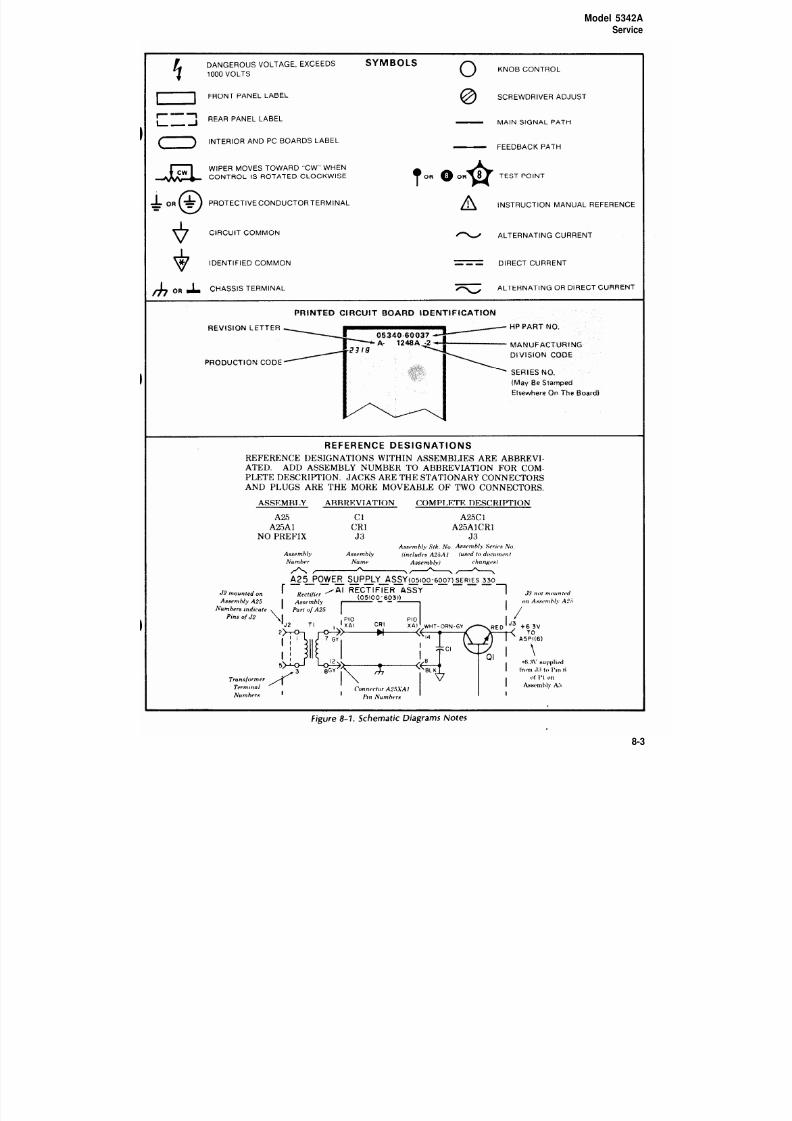
8/21/2019 HP5432 Microwave Frequency Counter
http://slidepdf.com/reader/full/hp5432-microwave-frequency-counter 163/364
Figure 8-1.
Model 5342AService
8-3

8/21/2019 HP5432 Microwave Frequency Counter
http://slidepdf.com/reader/full/hp5432-microwave-frequency-counter 164/364
Model 5342A
Service
8-11. Assembly Identification
8-12. The assembly number, name, and Hewlett-Packard part number of 5342A assemblies arelisted in Table 8-1.
Table 8-1. Assembly Identification
ASSEMBLY NAME HP PART NO.
A1 Keyboard Display 05342-60001A2 Display Driver 05342-60002A2 ( Option 004 (DAC Display Driver 05342-60028A3 Direct Count Amplifier 05342-60003A4 Offset VCO 05342-60004
— —.
A5 RF Multiplexer 05342-60005A6 Offset Loop Amplifier
Mixer/Search Control
05342-60006A7 05342-60007A8 Main VCO 05342-60008A9 Main Loop Amplifier 05342-60009
A10 Divide-by-N 05342-60010A1 1 IF Limiter 05342-60011A12 IF Detector 05342-60012
A13 Counter 05342-60013A14 Processor 05342-60014
A15 Option 011 HP-16 05342-60015A16 Option 002 Amplitude Measurements 05342-60038A16 Option 003 Extended Dynamic Range 05342-60037A17 Timing Generator 05342-60017A18 Time Base Buffer 05342-60018
A19 Primary Power 05342-60019A20 Secondary power 05342-60020A21 Switch Drive 05342-60021A22 Motherboard 05342-60022A23 Power Module 05342-60023
A24 Oscillator 05341-60047A24 Option 001 Oscillator 10544-60011A25 Preamplifier 05342-60025A26 Sampler Driver 05342-60026U1 Sampler 5088-7022
U2 Option 002 High Frequency Amplitude Module 5088-7035U2 Option 003 Attenuator 5088-7038
A27 Option 002 Low Frequency Amplitude Module 05342-60027A29 Option 011 HP-IB Interconnection 05342-60029
8-13. SAFETY CONSIDERATIONS
8-14, Although this instrument has been designed in accordance with international safetystandards, this manual contains information, cautions, and warnings which must be followed to
ensure safe operation and to retain the instrument in safe condition. Service and adjustmentsshould be performed only by service-trained personnel.
ANY INTERRUPTION OF THE PROTECTIVE(GROUNDING) CONDUCTOR (INSIDE OR OUT-SIDE THE INSTRUMENT) OR DISCONNECTION OFTHE PROTECTIVE EARTH TERMINAL IS LIKELY TOMAKE THE INSTRUMENT DANGEROUS. INTEN-TIONAL INTERRUPTION IS PROHIBITED.
8-4

8/21/2019 HP5432 Microwave Frequency Counter
http://slidepdf.com/reader/full/hp5432-microwave-frequency-counter 165/364
Model 5342AService
8-15. Any adjustment, maintenance, and repair of the opened instrument under voltage shouldbe avoided as much as possible and, when inevitable, should be carried out only by a skilledperson who is aware of the hazard involved.
8-16. Capacitors inside the instrument may still be charged even if the instrument has beendisconnected from its source of supply.
8-17. Make sure that only fuses with the required rated current and of the specified type(normal blow, time delay, etc.) are used for replacement. The use of repaired fuses and the short-circuiting of fuseholders must be avoided.
PRIOR TO MAKING ANY VOLTAGE TESTS ON THE
A19 PRIMARY POWER ASSEMBLY, THE VOLTMETER
TO BE USED OR THE 5342A MUST BE ISOLATED
FROM THE POWER MAINS BY USE OF AN lSOLA-
TION TRANSFORMER. A TRANSFORMER SUCH AS
AN ALLIED ELECTRONICS, 705-0084 (120V AC) MAY
BE USED FOR THIS PURPOSE. CONNECT THE
TRANSFORMER BETWEEN THE AC POWER SOURCEAND THE POWER INPUT TO THE 5342A.
8-18. Safety Symbols
8-19. The following safety symbols are used on equipment and in manuals:
Instruction manual symbol. The product will be marked with this symbolwhen it is necessary for the user to refer to the instruction manual inorder to protect against damage to the instrument.
Indicates dangerous voltage (terminals fed from the interior by voltageexceeding 1000 volts must be so marked).
Protective conductor terminal. For protection against electrical shock in
case of a fault. Used with field wiring terminals to indicate the terminalwhich must be connected to ground before operating equipment.
Low-noise or noiseless, clean ground (earth) terminal. Used for a signalcommon, as well as providing protection against electrical shock in caseof a fault. A terminal marked with the symbol must be connected toground in the manner described in the installation (operating) manual,and before operating the equipment.
Frame and chassis terminal. A connection to the frame (chassis) of theequipment which normally includes all exposed metal structures.
Alternating current (power line).
Direct current (power line).
Alternating or direct current (power line).
The WARNING signal denotes a hazard. It calls attention to a procedure,
practice, or the like, which, if not correctly performed or adhered to,
could result in personal injury.
The CAUTION sign denotes a hazard. It calls attention to an operatingprocedure, practice, or the like, which if not correctly performed oradhered to, could result in damage to or destruction of part or all of theproduct.
8-5

8/21/2019 HP5432 Microwave Frequency Counter
http://slidepdf.com/reader/full/hp5432-microwave-frequency-counter 166/364
Model 5342A
Service
8-20. SIGNAL NAMES
8-21. Table 8-2 is a list of signal names used in the 5342A. The list is in alphabetical order and
includes the mnemonics for cross-reference with the schematic diagram signal names. A descrip-
tion of the function of each signal and the source and destination is included in the table.
Tab le 8-2. Signa l Name s
8-6

8/21/2019 HP5432 Microwave Frequency Counter
http://slidepdf.com/reader/full/hp5432-microwave-frequency-counter 167/364
Model 5342AService
Tab le 8-2 Signa l Name s (Co ntinued )
MINEMONIC NAME FROM T O FUNCTION
CHECK Check Output XA10(11) XA11&7, 7 75 MHz signal sent from A1CDivide-by-N to All IFLimiter when 5342A is inCHECK mode,
CLOCK Clock XA17(4) XA14B(8, 8) 1 MHz TTL clock sent from(CLK) A17 Timing Generator to A14
Microprocessor clockgenerator to derive 1 andø2 from MPU.
DIRECT A Direct Count XA3(2) XA13(7) Divide-by-two output ofA Output Direct Count Amplifier
Assembly to A13 CounterAssembly.
DIRECT B Direct Count XA3(1) ,XA13(14) Divide-by-four output ofB Output Direct Count Amplifier
Assembly to A13 CounterAssembly.
DIV N Divide-by-N XA8(5) XAI0(8) Signal from A8 Main VCOto Al0 Divide-by-N.
DØ Data 0 XA14A(3) XA9(9), XAI0(15), XA13(1),
XA14A(3), XA15A(3),XA16A(3), XA17(10),A22J1(20), X22W4(11)
D1 Data 1 XA14A(4) XA10(16), XA13(2),XA17(11), A22J1(19),A22W4(12)
D2 Data 2 XA14A(5) XA10(17) XA13(3),XA15A(5), XA16A(5),XA17(12), A22J1 (18),A22W4(13)
D3 Data 3 XA14(6) XA10(18), XA13(4);XA15A(6), XA16A(6),XA17(13), A22J1 (17),A22W4(14)
D4 Data 4 XA14A(7) XA10(15), XA12(15, 15), Data Lines
XA15A(7), XA16A(7),XA17(11), A22J1 (5),A22W4(15)
D5 Data 5 XA14A(8) XA10(16), XA12(16, 16),XA15A(8), XA16A(8),XA17(10), A22J1 (6),A22W4(16)
D6 Data 6 XA14A(9) XA10(17), XA12(17, 17)XA15A(9), XA16A(9),XA17(9), A22J1 (7),A22W4(23)
D7 Data 7 XA14A(10) XA10(18), XA12(18, 18),XAI5AJ10), XA16A(10),
XA17(8), A22J1(8),A22W4(24)
EXT IN External Input J2 (rear panel) XA18(10) Signal from an externalsource via J2 on rear panelto A18 Time Base BufferAssembly
REQ ON F requency On XA16B(3) U2 Option 002 signal fromA16 board to U2 HF Ampto select frequencymeasurement.
8-7

8/21/2019 HP5432 Microwave Frequency Counter
http://slidepdf.com/reader/full/hp5432-microwave-frequency-counter 168/364
Model 5342A
ServiceTable 8-2. Signal Names (Continued)
8-8
MNEMONIC NAME FROM T O FUNCTION
HECL RST High ECL Reset XAI3(10) XA3(4) High signal from A13 Coun-
(HECLR) ter Assembly that resets themain gate on A3 DirectCount Amplifier Assembly.
HDSP WRT High Display XA14B(10) XA2(3) High signal from A14 Micro-(HDSP) Write processor causes data from
bus to be written into RAMon A2 Display Driver. Whensignal goes low, contents ofRAM are displayed.
HSRCH EN High Search XA7(2) XA6(8) High signal from 500 kHzEnable detector on A7 sent to
Search Generator on A6 ifthe offset VCO frequency isnot 500 kHz less than themain VCO frequency.
IF Intermediate A25J1 XA11(1), via A22W3 A25 Preamplifier output toFrequency All IF Limiter Assembly.
IF COUNT Intermediate XA12(8) XA13(7) A12 IF Detector output to
Frequency to A13 Counter AssemblyCounter
IF LIM Intermediate XA11(12) XA12(1) All IF Limiter output toFrequency A12 IF Detector Assembly.
Limiter Output
IF OUT Intermediate A25J2 j4 (rear panel) via W3 A25 Preamplifier interme-Frequency diate frequency output to
output rear panel connector.
ISOLATOR Optical Isolator XA19(18, 18) XA20(15, 15), XA21(17, 17) Signals excessive currentload to the U3 Timer Over-current shutdown circuit.
LAMPEN Low Amplitude XA16B(1) XA14B(Z Signal from A16 Amplitude
Option 002) Enable Assembly to notify A14Microprocessor that Option002 is present.
AMP MTR Low Amplitude XA14B(13) XA16B(2) Signal from A14 Microproc-
Option 002 ) Meter essor Assembly to write dataor read data from Option 002A16 Amplitude Assembly.
LCTR RD Low Counter XA14B(2) XA13(6) Signal from A14 Microproc-Read essor to A13 Counter Multi-
plexer circut to read con-tents of A or B counter to thedata bus (depending uponthe state of the AS line).
LCTR WRT Low Counter XA14B(3) XA13(7) Signal from A14 Microproc-Write9
essor to A13 Counter FF cir-cuit that selects either IF orDirect B to be counted.
LDA Low Digital-to- XA14B(3 XA2U15(4, 5) Signal from A14 Microproc-
Analog essor that loads data intoU15 Buffer register on A2board (Option 004) forconversion to analog.

8/21/2019 HP5432 Microwave Frequency Counter
http://slidepdf.com/reader/full/hp5432-microwave-frequency-counter 169/364
Model 5342AService
Table 8-2. Signal Names (Continued)
MNEMONIC NAME F R O M T O F UNCT ION
LDIRECT Low Direct XA13(14) XA16B(7) Signal from A13 Counter thatswitches A27 LF Amp or U2HF Amp to A16 boardmeasurement circuits.
LDI R Low Direct Gate XA17(4) XA3(5) Low signal from A17 TimingGate Generator that enables the
direct count main gate onA3 Direct Count AmplifierAssembly.
LDVRST Low Device XA14B(4) XA2J1(9) Temporary low signal fromReset A14 Microprocessor to A2
Display that blanks the dis-play during power up.
LEXT Low External S4 (rear panel) XA18(9) Low signal from rear panelswitch (EXT/l NT) in EXTposition that selects externaloscillator input to A18 Time
Base Buffer instead ofinternal oscillator.
LFM Low Frequency S3 (rear panel) XA17(12) Low signal from rear panel
Modulation switch (CW/FM) in FMposition that selects longprs and illuminates FM indi-cator on display.
LFRERUN Low Free Run XA14B(7 A14S2 (Ground) Low signal cause MPU on
(LFRUN) A14 Microprocessor to con-tinuously increment theaddresses on the address bus(for diagnostic purposes).
LHP-IB Low HP XA14B(14) XA15B(6) Low signal from decoder on
Interface Bus A14 Microprocessor to en-able reading from andwriting to A15 HP-IB(Option 011).
LIF Gate Low lnter- XA17(5) XA13(16) Low signal from A17 Timingmediate Fre- Generator that enables coun-
quency Gate ter A or B on A13 CounterAssembly (depending uponthe state of the LO switchsignal).
LIRQ Low Interrupt XA2J1(1) XA14A(13) Low signal from A2 DisplayRequest Driver or HP-IB Option 011
that interrupts A14 Micro-processor.
LKBRD Low Keyboard XA14B(9) XA2(4) Low signal enables A2 DisplayL K B R ) Driver to send keyboard
information to A14Microprocessor.
LO FREQ Local Oscillator A4W1 A26J2 A5 Multiplexer Local Oscil-Frequency Iator output to A26 Sampler
Driver.
8-9
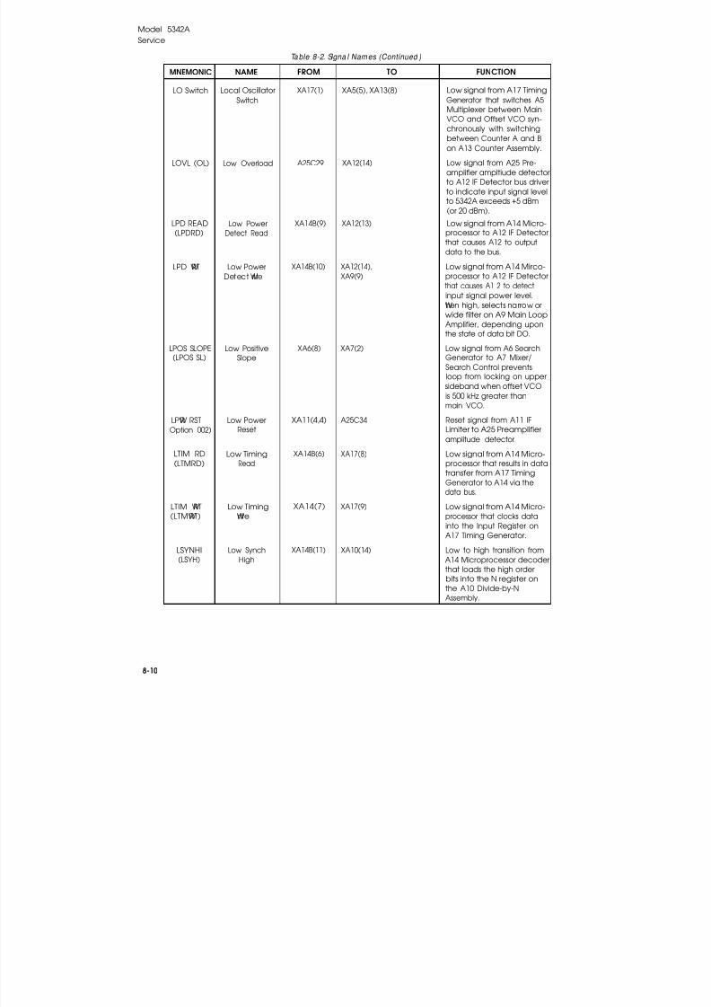
8/21/2019 HP5432 Microwave Frequency Counter
http://slidepdf.com/reader/full/hp5432-microwave-frequency-counter 170/364
Model 5342AService
Ta ble 8-2. Signa l Nam es (Continued )
MNEMONIC NAME FROM TO FUNCTION
LO Switch Local Oscillator XA17(1) XA5(5), XA13(8) Low signal from A17 TimingSwitch Generator that switches A5
Multiplexer between MainVCO and Offset VCO syn-chronously with switching
between Counter A and Bon A13 Counter Assembly.
LOVL (OL) Low Overload A25C29 XA12(14) Low signal from A25 Pre-amplifier ampltiude detectorto A12 IF Detector bus driverto indicate input signal levelto 5342A exceeds +5 dBm(or 20 dBm).
LPD READ Low Power XA14B(9) XA12(13) Low signal from A14 Micro-(LPDRD) Detect Read processor to A12 IF Detector
that causes A12 to outputdata to the bus.
LPD WRT Low Power XA14B(10) XA12(14), Low signal from A14 Mirco-Detect Write XA9(9) processor to A12 IF Detector
that causes A1 2 to detectinput signal power level.When high, selects narrow orwide filter on A9 Main LoopAmplifier, depending uponthe state of data bit DO.
LPOS SLOPE Low Positive XA6(8) XA7(2) Low signal from A6 Search(LPOS SL) Slope Generator to A7 Mixer/
Search Control preventsloop from locking on uppersideband when offset VCOis 500 kHz greater thanmain VCO.
LPWR RST Low Power XA11(4,4) A25C34 Reset signal from A11 IFOption 002) Reset Limiter to A25 Preamplifier
amplitude detector.
LTIM RD Low Timing XA14B(6) XA17(8) Low signal from A14 Micro-(LTMRD) Read processor that results in data
transfer from A17 TimingGenerator to A14 via thedata bus.
LTIM WRT Low Timing XA14(7) XA17(9) Low signal from A14 Micro-(LTMWRT) Write processor that clocks data
into the Input Register onA17 Timing Generator.
LSYNHI Low Synch XA14B(11) XA10(14) Low to high transition from(LSYH) High A14 Microprocessor decoder
that loads the high orderbits into the N register onthe A10 Divide-by-NAssembly.
8-10

8/21/2019 HP5432 Microwave Frequency Counter
http://slidepdf.com/reader/full/hp5432-microwave-frequency-counter 171/364
Model 5342AService
Table 8-2. Signa l Name s (Co ntinued ). ,
MNEMONIC NAME FROM TO FUNCTION
LSYNLO Low Synch XA14B(12) XA10(14) Low to high transition from(LSYL) Low A14 Microprocessor decoder
that loads low order bitsinto N register.
LXROM Low External XA15A(16), XA14A(16) Not used.R O M XA16A(16)
M AI N Main Phase XA10(1) XA9(12) Phase error signals fromError 1 A10 Divide-by-N assembly
to A9 Main Loop AmplifierM A I N Main Phase XA10(1) XA9(12) that control the A8 Main
Error 2 Main VCO.
MAIN CTRL Main Control XA9(6) XA8(1) Control voltage signal fromA9 Main Loop Amplifierthat controls the frequencyof the A8 Main VCO.
MAIN OSC Main Oscil lator XA8(7) XA5(10) A8 Main VCO output to A5RF Multiplexer Assembly.
MAIN VCO Main Voltage XA8(3) XA7(12) A8 Main VCO output to A7ControlledOscillator
Mixer/Search ControlAssembly that is mixed withthe signal from A4 OffsetVCO.
OFFSET Offset Phase 1 XA7(1) XA6(10) A7 Mixer/Search Controloutputs that are processedby A6 Offset Loop Amplifier
OFFSET Offset Phase 2 XA7(1) XA6(10) to develop OFFSET CON-TROL signal.
OFS CNTRL Offset Control XA6(6) XA4(5) A dc control voltage signalfrom A6 Offset Loop Ampli-fier to A4 Offset VCOAssembly.
OFS OSC Offset XA4(10) XA5(1) A4 Offset VCO output to A5Oscillator RF Multiplexer Assembly.
OFS VCO Offset Voltage XA4(7) XA7(9) A7 Offset VCO output to A7Controlled Mixer/Search ControlOscillator Assembly.
500 kHz 500 kilohertz XA18(3) XA7(7), XA10(5, 5) 500 kHz signal from A18Time Base to the phase de-tector on A7 and to ÷10 cir-cuit on A10 Divide-by-NAssembly.
1 MHz 1 Megahertz XA18(1) XA12(10), XA17(6) 1 MHz signal from A18 Time
Base to A12 IF Detector andto the prs generator on A17Timing Generator.
10 MHz OUT 10 Megahertz XA18(5) J3 (rear panel) 10 MHz signal from A18Timeo u t Base to FREQ STD OUT con-
nector on rear panel.
8-11

8/21/2019 HP5432 Microwave Frequency Counter
http://slidepdf.com/reader/full/hp5432-microwave-frequency-counter 172/364
Model 5342A
Service
8-22. DISASSEMBLY AND REASSEMBLY
8-23. Before performing any of the following disassembly or reassembly procedures, the fol-lowing steps must be performed.
a.
b.
8-24.
8-25.
a.
b.
c.
d.
8-26.
8-27.
a.
b.
c.
d.
8-28.
8-29.
a.
b.
c.
d.
Set LINE ON-STBY switch to STBY position.
Remove line power cable from Input Power Module (A23).
Top Cover Removal
To remove the top cover proceed as follows:
Place 5342A with top cover facing up.
At top rear of instrument remove pozidrive screw from rear cap retainer and removeretainer,
Slide top cover back until free from frame and lift off.
To gain access to pc assemblies remove screws from top plate and remove plate.
Bottom Cover Removal
To remove the bottom cover proceed as follows:
Place 5342A with bottom cover facing up.
In the following step, the two front plastic feet mustbe removed from the bottom panel to avoid damageto internal wiring.
Remove two front plastic feet from bottom cover, Lift upon back edge of plastic foot andpush back on front edge of plastic foot to free foot from bottom cover.
Loosen captive pozidrive screw at rear edge of bottom cover.
Slide bottom cover back until it clears the frame. Reverse the procedure to replace thecover.
FRONT FRAME REMOVAL
To remove front frame from main housing of the instrument, proceed as follows:
Remove top and bottom covers as described in preceding paragraphs,
Remove nut from type N connector on front panel.
Remove two screws from front of each side strut attaching front panel frame.
From bottom front of instrument, remove coax cable by pulling off connectors from A1J1and A1J3. Remove cable strap connector from A2 Display Driver board. Note orientationof connector pins for reference during reassembly,
In the following step, note the cable attached to thepower LINE switch and avoid stress on cable connec-
tions during removal of front panel frame.
8-12

8/21/2019 HP5432 Microwave Frequency Counter
http://slidepdf.com/reader/full/hp5432-microwave-frequency-counter 173/364
e.
f.
Model 5342AService
Slowly slide front panel frame off while pressing type N connector rearward throughpanel.
The front panel frame (containing assemblies A1 and A2) can now be moved freely withinlimits of the power cable, as shown in Figure 8-2.
8-30. Removal of Al Display Assembly and A2 Display Drive Assembly from
Front Panel Frame
8-31. To remove A1 and A2 assemblies, remove frame as described in above paragraph andproceed as follows:
a. Remove the A1-A2 assemblies (combined) from front panel frame by removing the nutfrom the front panel BNC connector and removing the 5 large attaching screws from A2Display Driver board,
b. Separate the Al and A2 assemblies by removing the two nuts attaching plug P1 on the AlDisplay assembly. Do not remove the attached screws from A2 Display Driver assembly.
c. Reassembly procedures are essentially the reverse of the disassembly procedures.
8-32. Replacement of LED’s in Front Panel Switches
8-33. To replace a defective LED in a front panel pushbutton switch, remove and separate the Aland A2 boards as described in the preceding paragraphs, and proceed as follows:
a.
b.
c.
d.
8-34.
8-35.
a.
b.
c.
d.
e.
f.
g.
h.
i.
j.
Pull off the switch cap that covers the defective LED.
Use a short length (approximately 2 inches) of heat-shrink tubing that will fit over thereplacement LED. Apply heat to the tubing to make a tight fit.
Unsolder the connections to the defective LED on the Al board. Slide the heat-shrinktubing over the defective LED and withdraw.
Place the replacement LED into the heat-shrink tubing and insert into the switch. Solderthe leads to the board.
Removal of U1 Sampler, A25 Preamplifier, and A26 Sampler Driver
Remove U1, A25, and A26 as follows:
Remove 5342A bottom panel by loosening screw at rear, remove two front feet and slidepanel rearward.
Refer to Figure 8-22 and locate assemblies at bottom front of instrument.
Pull off coax cables from A1J1, A1J3, A25J1 (IF OUT INT), and A25J2 (IF OUT EXT).
Disconnect rigid coax from U1 Sampler by loosening attaching nut.
Remove nut on front panel type N connector and remove rigid cable to allow access.
Remove W2 cable strap connector at A22 motherboard and move cable strap to one sideto allow access.
Remove 5 screws attaching A25 mounting bracket (four corner and one middle screw)and withdraw bracket (and attached assemblies) from intrument.
Remove A26 from bracket by removing the 2 smalI attaching bolts and nuts. Separate A26from U1 by loosening the interconnecting hex connector from U1. Remove the coverfrom A26 to gain access to components,
Remove U1 by removing one small bolt and nut, Pull U1 up out of socket.
Assembly procedures are essentially the reverse order of the disassembly.
8-13

8/21/2019 HP5432 Microwave Frequency Counter
http://slidepdf.com/reader/full/hp5432-microwave-frequency-counter 174/364
Figure 8-2.
Model 5342A
Service
8-14

8/21/2019 HP5432 Microwave Frequency Counter
http://slidepdf.com/reader/full/hp5432-microwave-frequency-counter 175/364
Model 5342AService
8-36. FACTORY SELECTED COMPONENTS
8-37. Some component values are selected at the time of final checkout at the factory. Thesevalues are selected to provide optimum compatibility with associated components and areidentified on schematics and parts lists by an asterisk (*). The recommended procedure forreplacing a factory-selected part is as follows:
a. Refer to paragraphs 8-38 through 8-45 for test procedures required for selection ofcritical value parts.
b. For factory selected components that are not listed in paragraphs 8-38 through 8-45, usethe original value,
c. After replacing parts, perform the test specified for the circuit in the performance andadjustment sections of this manual to verify correct operation.
8-38. Procedure for Selecting Resistor R15 on Direct Count Amplifier A3
8-39. If resistor A3R15 is not properly selected for value (average value 42.2 ohms), the 5342Amay exhibit a miscount at the low frequency direct count input for frequencies near 500 MHz.To properly select A3R15, perform the following:
a. Set the 5342A to the 10 Hz-500 MHz RANGE and select 1 kHz RESOLUTION.
b. With assembly A3 on an extender board, monitor A3U4(14) with an oscilloscope.
c. The signal at A3U4(14) must go positive by 100 mV (±25 mV).
d. To determine the value of A3R15, first decide how much the actual upper voltage level atA3U4(14) must change in order to fall between +75 mV to +125 mV. For every 5 mVincrease required, the value of A3R15 must be increased by 1 ohm and for every 5 mVdecrease, the value of A3R15 must be decreased by 1 ohm. For example, if the actualvoltage only goes positive by 25 mV, then a 75 mV increase is required. Increase A3R15by 1
e. Use a 1%, 0.125Wresistor for A3R15, The following are HP part numbers for resistorswhich may be used.
Value Part No.
8-15
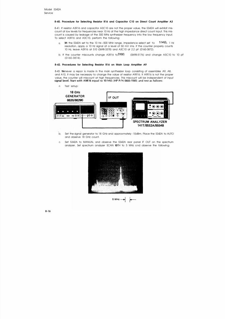
8/21/2019 HP5432 Microwave Frequency Counter
http://slidepdf.com/reader/full/hp5432-microwave-frequency-counter 176/364
Model 5342AService
8-40. Procedure for Selecting Resistor R16 and Capacitor C10 on Direct Count Amplifier A3
8-41. If resistor A3R16 and capacitor A3C10 are not the proper value, the 5342A will exhibit mis-count at low levels for frequencies near 10 Hz at the high impedance direct count input. This mis-count is caused by leakage of the 300 MHz synthesizer frequency into the low frequency input.To select A3R16 and A3C10, perform the following:
With the 5342A set to the 10 Hz—500 MHz range, impedance select set to 1 Hza.resolution, apply a 10 Hz signal at a level of 50 mV rms. if the counter properly counts10 Hz, leave A3R16 at 510 (0698-3378) and A3C10 at 2.2 pF (0160-3872).
b. If the counter miscounts change A3R16 to (0698-5176) and change A3C10 to 10 pF(0160-3874).
8-42. Procedures for Selecting Resistor R16 on Main Loop Amplifier A9
8-43. Whenever a repair is made in the main synthesizer loop consisting of assemblies A9, A8,and A10, it may be necessary to change the value of resistor A9R16. If A9R16 is not the propervalue, the counter will miscount at high frequencies. This miscount will be independent of input
a. Test setup:
b. Set the signal generator to 18 GHz and approximately -10dBm. Place the 5342A to AUTOand observe 18 GHz count.
c. Set 5342A to MANUAL and observe the 5342A rear panel IF OUT on the spectrumanalyzer. Set spectrum analyzer SCAN WIDTH to 5 MHz and observe the following:
8-16

8/21/2019 HP5432 Microwave Frequency Counter
http://slidepdf.com/reader/full/hp5432-microwave-frequency-counter 177/364
d. Reduce input signal level until counter no longer counts
The IF OUT on the spectrum analyzer should appear as:
Model 5342A
Service
18 GHz but displays all zeros.
e. If the spectrum analyzer display remains as in the first photo, or if the IF is centered as
shown below, then change A9R16 to 15 MO (0683-1565).
IF THIS IS CENTERED, THEN
CHANGE A9R16 to 15 ML
8-44. Procedure for Selecting Resistor A16R2 on A16 Assembly (Option 002 or 003)
8-45. When replacing resistor A16R2 (average value 10K ohms) select the original factoryselected value that is labeled on U2 assembly (part of Option 002 or 003).
8-17
8/21/2019 HP5432 Microwave Frequency Counter
http://slidepdf.com/reader/full/hp5432-microwave-frequency-counter 178/364
Model 5342A
Service
8 - 4 6 . S E R V I C E A C C E S S O R Y K I T 1 0 8 4 2 A
8-47. The 10842A Service Accessory Kit contains 10 special extender boards (Figure 8-3)designed to aid in troubleshooting the 5342A, The following paragraphs describe equipmentsupplied, replaceable parts and operation.
8-48. Equipment Supplied
8-49. Table 8-3 lists the boards contained in the 10842A Service Accessory Kit with their generaldescription and usage. The kit is shown in Figure 8-3.
Table 8-3. 10842A Kit Conte nts
HP PART NO. I QTY. I DESCRIPTION FOR USE
05342-60030 1 10 pin X2 Extender Boards for A4, A5, A6, and A18 assemblies.
05342-60031 1 12 pin X2 Extender Boards for A3, A7, A8, A9, and All assemblies.
05342-60032 1 15 pin X2 Extender Boards for the A24 assembly.
05342-60033 2 18 pin X2 Extender Boards for the A17 assembly.
05342-60034 2 22 pin X2 Extender Boards for A10, A12, A13, A20, A21 assemblies.
05342-60035 1 24 pin X2 Extender Boards for the A19 assembly,
05342-60036 1 Double 18 pin X2 Extender Boards for the A14 assembly.
05342-60039 1 Keyed double 18 pin X2 Extender Boards for the A15 HP-16 assembly.
NOTE
For the Option 002 and 003 A16 assembly, use one05342-60030 (10 pin X2) Extender Board and one05342-60033 (18 pin X2) Extender Board,
8-50. Replaceable Parts
8-51. The only replaceable parts in the 10842A kit are the two integrated circuits and fiveswitches on the 05342-60036 extender board. Table 8-4 lists the HP part number and descriptionof those parts. Refer to Section VI for ordering information,
Table 8-4. Rep lac ea b le Pa rts for Extender Boa rd 05342-60036
Ref.DESIG.
HP PART NO. QTY. DESCRIPTION MFR PART NO.
U1 1820-1197 1 IC GATE TTL LS NAND QUAD 2-INPUT 01698 SN74LS00N
U2 1820-1281 1 IC DCDR TTL LS 2-TO-4-LINE DUAL 2-INPUT 01698 SN74LS139N
S1 3101-1856 1 SWITCH-SL-8-1A-NS DIP-SLIDE-ASSY .1A 28480 3101-1856
S2 3101-1856 1 SWITCH-SL-8-1A-NS DIP-SLIDE-ASSY .1A 28480 3101-1856
53 3101-1856 1 SWITCH-SL 8-1A-NS DIP-SLIDE-ASSY .1A 28480 3101-1856
54 3101-1213 1 SWITCH-TGL SUBMIN DPST ,5A 120VAC PC 28480 3101-1213
55 3101-1675 1 SWITCH-TGL SUBMIN DPST .5A 120VAC/ 28480 3101-1675DC PC
8-18

8/21/2019 HP5432 Microwave Frequency Counter
http://slidepdf.com/reader/full/hp5432-microwave-frequency-counter 179/364
Model 5342AService
Figure 8-3. 10842A Service Accessory Kit8-19
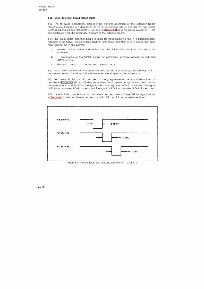
8/21/2019 HP5432 Microwave Frequency Counter
http://slidepdf.com/reader/full/hp5432-microwave-frequency-counter 180/364
Model 5342AService
8-52. Using Extender Board 05342-60036
8-53. The following paragraphs describe the general operation of the extender board(05342-60036), Included is a description of the 3 DIP switches (S1, S2, and S3) the two toggleswitches (S4 and S5) and test points R1, R2, and R3. Figure 8-4 shows the signals present at R1, R2,and R3, Figure 8-5 is the schematic diagram of the extender board.
8-54. The 05342-60036 extender board is used for troubleshooting the A14 MicroprocessorAssembly in the 5342A. This extender board not only allows operation of A14 outside the instru-ment casting but it also permits:
a. Isolation of the 16-line address bus and the 8-line data bus from the rest of theinstrument.
b. Generation of START/STOP signals for performing signature analysis on individualROM’s on A14,
c. Manual control of the microprocessor reset .
8-55. The S1 switch (leftmost switch) opens the data bus. With all switches up, the switches are inthe closed position. The S2 and S3 switches open the 16 lines of the address bus.
8-56. Test points R1, R2, and R3 are used in taking signatures of the A14 ROM outputs asdescribed in Table 8-9. U1 and U2 decode address lines to generate signals which bracket theaddresses of each specific ROM. The signal at R1 is Iow only when ROM U1 is enabled. The signalat R2 is low only when ROM U4 is enabled. The signal at R3 is Iow only when ROM U7 is enabled.
8-57. If the A14 Microprocessor is put into free-run as described in Table 8-9, the signals shownin Figure 8-4 should be observed at test points R1, R2, and R3 on the extender board.
Figure 8-4. Extender Board (05342-60036) Test Points R1, R2, and R3
8 - 2 0

8/21/2019 HP5432 Microwave Frequency Counter
http://slidepdf.com/reader/full/hp5432-microwave-frequency-counter 181/364
Model 5342AService
Figure 8-5. Extend er Board (05342-60036) Schem atic Diagra m
8-21

8/21/2019 HP5432 Microwave Frequency Counter
http://slidepdf.com/reader/full/hp5432-microwave-frequency-counter 182/364
Model 5342AService
8-58. LOGIC SYMBOLS
8-59. Logic symbols used in this manual conform to the American National Standard ANSIY32.14-1973 (IEEE Std. 91-1973). This standard supersedes MIL-STD-806B. In the following para-graphs logic symbols are described. For further descriptions refer to HP Logic Symbologymanual, part number 5951-6116.
8-60. Logic Concepts
8-61. The binary numbers 1 and 0 are used in pure logic where 1 represents true, yes, or activeand 0 represents false, no, inactive. These terms should not be confused with the physicalquantity (e.g., voltage) that may be used to implement the logic, nor should the term “active” beconfused with a level that turns a device on or off, A truth table for a relationship in logic shows(implicitly or explicitly) all the combinations of true and false input conditions and the result(output). There are only two basic logic relationships, AND and OR. The following illustrationsassume two inputs (A and B), but these can be generalized to apply to more than two inputs.
AND Y is true if and only if A is true and B is OR Y is true if and only if A is true or B is truetrue (or more generally, if all inputs are (or more generally, if one or more input(s)
true). is (are) true).Y=1 if and only if A=1 and B=1 Y=1 if and only if A=1 or B=1y=A•B Y=A+B
TRUTH TABLE
8-62. Negation
EQUIVALENTSYMBOLS TRUTH TABLE
EQUIVALENTSYMBOLS
8-63. In logic symbology, the presence of the negation indication symbol o provides for thepresentation of logic function inputs and outputs in terms independent of their physical values,the Ø-state of the input or output being the l-state of the symbol referred to the symboldescription.
8-22
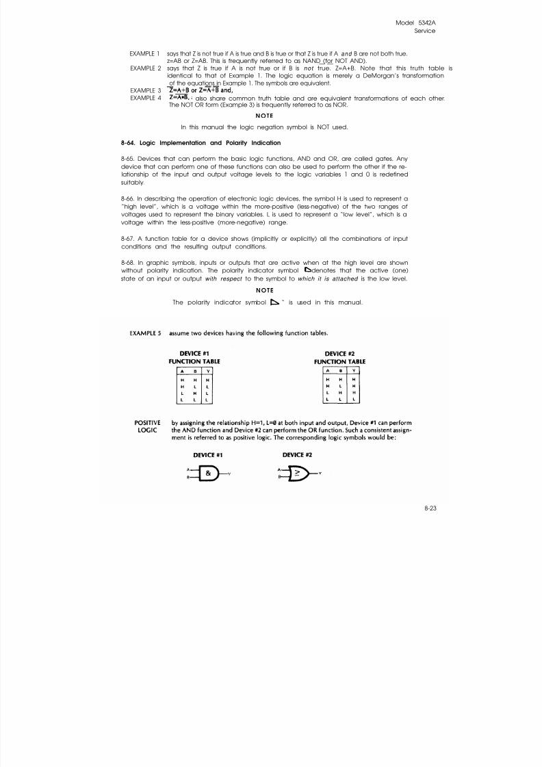
8/21/2019 HP5432 Microwave Frequency Counter
http://slidepdf.com/reader/full/hp5432-microwave-frequency-counter 183/364
Model 5342AService
EXAMPLE 1
EXAMPLE 2
EXAMPLE 3EXAMPLE 4
says that Z is not true if A is true and B is true or that Z is true if A and B are not both true.z=AB or Z=AB. This is frequently referred to as NAND (for NOT AND).says that Z is true if A is not true or if B is not true. Z=A+B. Note that this truth table is
— —
identical to that of Example 1. The logic equation is merely a DeMorgan’s transformationof the equations in Example 1. The symbols are equivalent.— —
also share common truth table and are equivalent transformations of each other.
The NOT OR form (Example 3) is frequently referred to as NOR.NOTE
In this manual the logic negation symbol is NOT used.
8-64. Logic Implementation and Polarity Indication
8-65. Devices that can perform the basic logic functions, AND and OR, are called gates. Anydevice that can perform one of these functions can also be used to perform the other if the re-lationship of the input and output voltage levels to the logic variables 1 and 0 is redefinedsuitably.
8-66. In describing the operation of electronic logic devices, the symbol H is used to represent a
“high level”, which is a voltage within the more-positive (less-negative) of the two ranges ofvoltages used to represent the binary variables. L is used to represent a “low level”, which is avoltage within the less-positive (more-negative) range.
8-67. A function table for a device shows (implicitly or explicitly) all the combinations of inputconditions and the resulting output conditions.
8-68. In graphic symbols, inputs or outputs that are active when at the high level are shownwithout polarity indication. The polarity indicator symbol denotes that the active (one)state of an input or output with respect to the symbol to which it is attached is the low level.
NOTE
The polarity indicator symbol “ “ is used in this manual.
8-23

8/21/2019 HP5432 Microwave Frequency Counter
http://slidepdf.com/reader/full/hp5432-microwave-frequency-counter 184/364
8-24
Model 53424Service
NEGATIVE alternatively, by assigning the relationship H=Ø, L=1 at both input and output, Device LOGIC can perform the OR function and Device #2 can perform the AND function. Such a con
sistent assignment is referred to as negative logic. The corresponding logic symbols woube:
DEVICE #l DEVICE #2
8-69. MIXED LOGIC. The use of the polarity indicator symbol ( ) automatically invokes amixed-logic convention. That is, positive logic is used at the inputs and outputs that do not havepolarity indicators, negative logic is used at the inputs and outputs that have polarity indicators.
This may be shown either of two ways:
Note the equivalence of these symbols toexamples 1 and 2 and the fact that thefunction table is a positive-logic translation(H=1, L=Ø) of the NAND truth table, andalso note that the function table is thenegative-logic translation (H=Ø, L=1) of theNOR truth table, given in Example 3.
This may be shown either of two ways:
Note the equivalence of these symbols toexamples 3 and 4 and the fact that thefunction table is a positive-logic translation(H=1, L=Ø) of the NOR truth table, andalso note that the function table is thenegative-logic translation (H=Ø, L=1 ) of thethe NAND truth table, given in Example 1.
8-70. It should be noted that one can easily convert from the symbology of positive-logic
distinctive shape alone. To convert from the symbology of negative-logic, a polarity indication
shape or vice versa.
8-71. It was shown that any device that can perform OR logic can also perform AND logic andvice versa. DeMorgan’s transformation is illustrated in Example 1 through 7. The rules of the
transformation are:1. At each input or output having a negation (o) or polarity ( ) indicator, delete the
indicator.
2. At each input or output not having an indicator, add a negation (o) or polarity ( )indicator.
3. Substitute the AND symbol for the OR symbol or vice versa.
These steps do not alter the assumed convention; positive-logic stays positive, negative-Iogic stays negative, and mixed-logic stays mixed.

8/21/2019 HP5432 Microwave Frequency Counter
http://slidepdf.com/reader/full/hp5432-microwave-frequency-counter 185/364
Model 5342AService
8-72. The choice of symbol maybe influenced by these considerations: (1) The operation beingperformed may best be understood as AND or OR. (2) In a function more complex than a basicgate, the inputs will usually be considered as inherently active high or active low (e.g., the J and Kinputs of a J-K flip-flop are active high and active low, respectively). (3) In a chain of logic, under-standing and the writing of logic equations are often facilitated if active low or negated outputsfeed into active low or negated inputs.
8-73.
8-74.
Other Symbols
Additional symbols are required to depict complex logic diagrams, as follows:
Dynamic input activated by transition from a low level to a high level. Theopposite transition has no effect at the output.
Dynamic input activated by transition from a high level to a low level. Theopposite transition has no effect at the output.
Exclusive OR function. The output will assume its indicated active level if and
only if one and only one of the two inputs assumes its indicated active level.
Inverting function. The output is low if the input is high and it is high if the inputis low. The two symbols shown are equivalent.
Noninverting function. The output is high if the input is high and it is low if theinput is low. The two symbols shown are equivalent.
OUTPUT DELAY. The output signal is effective when the input signal returnsto its opposite state.
EXTENDER. Indicates when a logic function increases (extends) the numberof inputs to another logic function.
FLIP-FLOP. A binary sequential element with two stable states: a set (1) stateand a reset (0) state. Outputs are shown in the 1 state when the flip-flop is set.In the reset state the outputs will be opposite to the set state.
RESET. A 1 input will reset the flip-flop. A return to 0 will cause no furthereffect.
SET. A 1 input will set the flip-flop. A return to 0 will cause no further action.
TOGGLE. A 1 input will cause the flip-flop to change state. A return to 0 willcause no further action.
8 - 2 5
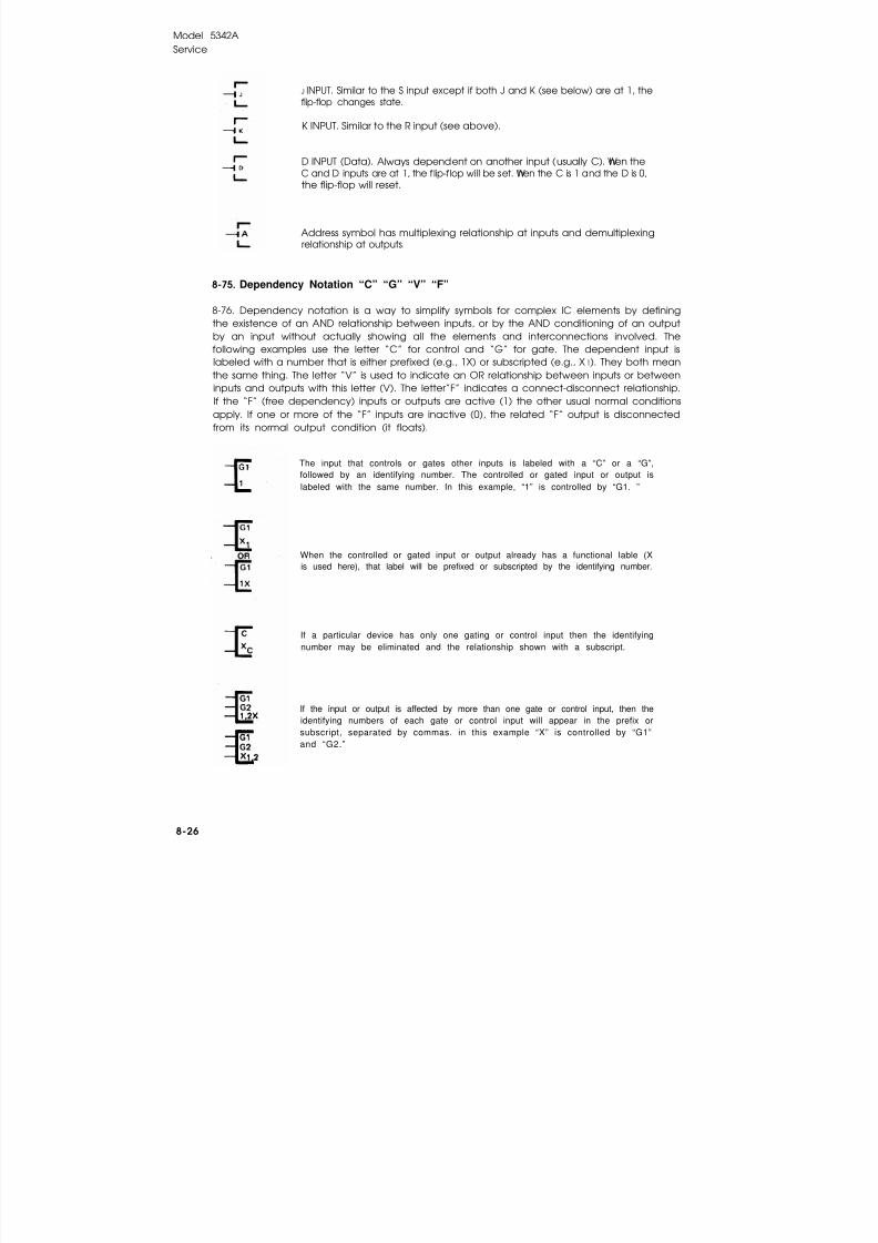
8/21/2019 HP5432 Microwave Frequency Counter
http://slidepdf.com/reader/full/hp5432-microwave-frequency-counter 186/364
Model 5342AService
J INPUT. Similar to the S input except if both J and K (see below) are at 1, theflip-flop changes state.
K INPUT. Similar to the R input (see above).
D INPUT (Data). Always dependent on another input (usually C). When theC and D inputs are at 1, the f lip-flop will be set. When the C is 1 and the D is 0,the flip-flop will reset.
Address symbol has multiplexing relationship at inputs and demultiplexingrelationship at outputs.
8-75. Dependency Notation “C” “G” “V” “F”
8-76. Dependency notation is a way to simplify symbols for complex IC elements by definingthe existence of an AND relationship between inputs, or by the AND conditioning of an output
by an input without actually showing all the elements and interconnections involved. Thefollowing examples use the letter “C” for control and “G” for gate. The dependent input islabeled with a number that is either prefixed (e.g., 1X) or subscripted (e.g., X 1). They both meanthe same thing. The letter “V” is used to indicate an OR relationship between inputs or betweeninputs and outputs with this letter (V). The letter”F” indicates a connect-disconnect relationship.If the “F” (free dependency) inputs or outputs are active (1) the other usual normal conditionsapply. If one or more of the “F” inputs are inactive (0), the related “F” output is disconnectedfrom its normal output condition (it floats).
The input that controls or gates other inputs is labeled with a “C” or a “G”,
followed by an identifying number. The controlled or gated input or output is
labeled with the same number. In this example, “1” is controlled by “G1. ”
When the controlled or gated input or output already has a functional Iable (X
is used here), that label will be prefixed or subscripted by the identifying number.
If a particular device has only one gating or control input then the identifying
number may be eliminated and the relationship shown with a subscript.
If the input or output is affected by more than one gate or control input, then the
identifying numbers of each gate or control input will appear in the prefix or
subscript, separated by commas. in this example “X” is controlled by “G1”
and “G2.”
8-26

8/21/2019 HP5432 Microwave Frequency Counter
http://slidepdf.com/reader/full/hp5432-microwave-frequency-counter 187/364
Model 5342AService
8-77. Control Blocks
8-78. A class of symbols fcr complex logic are called control blocks. Control blocks are used toshow where common control signals are applied to a group of functionally separate units.Examples of types of control blocks follow.
Register control block. This symbol is used with an associated array of flip-flopsymbols to provide a point of placement for common function lines, such as acommon clear.
Shift register control block. These symbols are used with any array of flip-flopsymbols to form a shift register. An active transition at the inputs causes leftor right shifting as indicated.
Counter control block. The symbol is used with an array of flip-flops or othercircuits serving as a binary or decade counter. An active transition at the +1 or-1 input causes the counter to increment one count upward or downward, re-spectively. An active transition at the ±1 input causes the counter to incrementone count upward or downward depending on the input at an up/down control.
Selector control block. These symbols are used with an array of OR symbols toprovide a point of placement for selection (S) or gating (G) lines. The selectionlines enable the input designated 0, 1 , . . . .n of each OR function by means of abinary code where S0 is the least-significant digit. If the 1 level of these lines islow, polarity indicators (h) will be used. The gating lines have an AND relationwith the respective input of each OR function: G1 with the inputs numbered 1,G2 with the input numbered 2, and so forth. If the enabling levels of these linesis low, polarity indicators ( ) will be used.
Output selector control block. This symbol is used with a block symbol having
multiple outputs to form a decoder. The selection lines enable the output de-signated 0, 1, . . . . n of each block by means of a binary code where S0 is the least-
be used.
8 - 2 7

8/21/2019 HP5432 Microwave Frequency Counter
http://slidepdf.com/reader/full/hp5432-microwave-frequency-counter 188/364
Model 5342A
Service
8-79. Complex Logic Devices
8-80. Logic elements can be combined to produce very complex devices that can perform moredifficult functions. A control block symbol can be used to simplify understanding of many com-plex devices. Several examples of complex devices are given here. These examples are typical ofthe symbols used in schematic diagrams in this manual.
Reference DesignationA2U2, A2U7
Part Number1820-0468
SN7445N
DescriptionBCD TO DECIMAL DECODER/DRIVER
The output which is low will correspond to the binary weighted input. The minussigns at the output indicate that the element is capable of supplying LOW’s only,
Reference DesignationA2U3Part Number1820-1443
SN74LS293N
Description4-BIT BINARY COUNTER
This binary counter has four master-slave flip-flops and gating for which the countcycle length is divide-by-eight. The counter has a gated zero reset. To use the maxi-
mum count length, the pin 11 input is connected to the pin 9 output. The inputcount pulses are applied to the pin 10 input.
Reference DesignationA2U8, A2U11
Part Number1820-0428
SN7489
Description64-BIT READ/WRITE MEMORY
This memory has an array of 64 flip-flop memory cells in a matrix to provide 16 wordsof 4 bits each, Information present at the data input (pins 4,6, 10, 12) is written intomemory by holding both the memory enable (pin 2) and write enable (pin 3) LOWwhile addressing the desired word at the BCD weighted inputs (pins 1, 13, 14, 15).The complement of the information written into memory is read out at the four out-puts by holding memory enable (pin 2) LOW, write enable (pin 3) HIGH and selec-ting the desired address,
8-28

8/21/2019 HP5432 Microwave Frequency Counter
http://slidepdf.com/reader/full/hp5432-microwave-frequency-counter 189/364
Model 5342A
Service
Reference DesignationA2U12, A2U16
Part Number1820-1254DM8095N
Reference DesignationA14U16, A14U18
Part Number1820-1368DM8096N
Reference DesignationA2U6
1820-1049DM8097N
Reference DesignationA14U8
Part Number1820-1255DM8098N
DescriptionHEX BUFFERS - HEX INVERTERS
The buffers (8095-8097) and inverters (8096-8098) convert standard TTL or DTL out-puts to THREE-STATE outputs. The 8095 and 8096 control all six devices fromcommon inputs (pins 1 and 15 LOW). The 8097 and 8098 control four devices fromone input (pin 1 LOW) and two devices from another input (pin 15 LOW).
Reference DesignationA2U17
Part Number1820-142874LS158
Description2-LINE TO 1-LINE DATA SELECTOR/MULTIPLEXER
This quad two input multiplexer selects one of two word inputs and outputs the datathe data when enabled. The level at pin 1 selects the input word. The outputs areLOWwhen pin 15 is LOW.
8-29
8/21/2019 HP5432 Microwave Frequency Counter
http://slidepdf.com/reader/full/hp5432-microwave-frequency-counter 190/364
Model 5342AService
Reference DesignationA2U18,A2U18, A9U1,A10U4, A12U13, A13U4,A14U9 A15U3, A15U4,A15U9, A15U10, A15U14,A15U19, A15U34, A15U34,A17U9, A17U15
Part Number1820-1112
SN74LS74N
DescriptionDUAL D-TYPE FLIP-FLOP
The dual D-type flip-flop consists of two independent D-type flip-flops. The infor-mation present at the data (Dc) input is transferred to the active-high and active-lowoutputs on a low-to-high transition of the clock (C) input. The data input is thenlocked out and the outputs do not change again until the next low-to-high tran-sition of the clock input. The set (S) and reset (R) inputs override all other input con-ditions: when (S) is low, the active-high output is forced high; when reset (R) is low,the active-high output is forced low. Although normally the active-low output is thecomplement of the active-high output, simultaneous low inputs at the set and reset
will force both the active-low and active-high outputs to go high at the same time onsome D-type flip-flops. This condition will exist only for the length of time thatboth set and reset inputs are held low. The flip-flop will return to some indeter-minate state when both the set and reset inputs are returned to the high state.
Reference DesignationA1U22
Part Number1820-0574DM8551N
Description4-BIT D-TYPE REGISTERS
When both data-enable inputs (9 and 10) are LOW, data at the D C inputs is loadedinto the flip-flops on the next positive transition of the clock (pin 7), When both out-puts control inputs (pins 1 and 2) are LOW, data is available at the outputs. The out-puts are disabled by a HIGH at either output control input. The outputs thenrepresent a high impedance.
8-30

8/21/2019 HP5432 Microwave Frequency Counter
http://slidepdf.com/reader/full/hp5432-microwave-frequency-counter 191/364
Model 5342A
Service
Reference Designation
A10U1, A13U13, A13U14
A13U17, A13U18
Part Number
1820-1251
SN74LS196N
Description50/30 MHz PRESETTABLE DECADE COUNTER/LATCH
The Decade Counter consists of a divide-by-two and a divide-by-five counterformed by connecting pin 5 to pin 6 and taking the output from pin 12.
The outputs may be preset to any state by making “C” active low and entering thedesired data at the “Dc” inputs. The outputs at pins 5, 9, 2, and 12 will then corre-spond to the data inputs independent of the state of the count-up clocks at pins 6and 8. An active high signal at pin 1 then enables the counter by Iatching the parallel
data into the counter. The count-up clock at pin 8 clocks the 2 counter and pin 6clocks the counter. When the counter is clocked at pins 8 or 6, the outputs willchange on the negative-going edge of the signal. An active low at the “R” (reset)input (pin 13) causes all the outputs to go low independent of the counting state.
Reference Designation
A10U8, A10U9,
A10U13, A10U14
Part Number
1820-1429
74LS160
DescriptionSYNCHRONOUS DECADE COUNTER
This synchronous presettable decade counter has four master slave flip-flops thatare triggered on the positive-going edge of the clock pulse (pin 2). A LOWat theload input (pin 9) disables the counter and causes the outputs to agree with thesetup data after the next clock pulse regardless of the levels at the enable inputs(pins 7 and 10). The clear function (pin 1) is asynchronous and a low level clear inputsets all outputs low regardless of the levels of the clock, load or enable inputs. Bothcount enable inputs (pins 7 and 10) must be HIGH to count and the pin 10 input is fedforward to neable the carry output (pin 15).
8-31

8/21/2019 HP5432 Microwave Frequency Counter
http://slidepdf.com/reader/full/hp5432-microwave-frequency-counter 192/364
Model 5342A
Service
Reference DesignationA10U10, A10U15, A10U17
Part Number1820-1196SN74LS174N
Reference DesignationA1W11, A10U16
Part Number1820-1195SN74LS175N
DescriptionHEX/QUAD D-TYPE FLIP-FLOPS
Information at the D inputs is transferred to the outputs on the positive-edge of the
clock pulse (pin 9). Clock triggering occurs at a particular voltage level. The hex FFshave single outputs, the quad FFs have complementary outputs.
Reference DesignationA12U10, A12U15
Part Number1820-1193SN74LS197N
Description30 MHz PRESETTABLE BINARY
COUNTERS/LATCHES
This counter consists of four master-slave flip-flops that form a divide-by-two and a
divide-by-eight counter. The outputs may be preset to any state by placing a low on
pin 1 and entering the desired data. The outputs will change to agree with the inputsregardless of the state of the clocks. When used as a high-speed 4-bit ripple-through
counter, the output of pin 5 must be externaly connected to the clock 2 input (pin
6). The input count pulses are applied to the clock 1 input (pin 8). Simultaneousdivisions by 2, 4, 8, and 16 are performed at output pins 12, 2, 9, and 5, respectively.
When used as a 3-bit ripple-through counter, the input count pulses are applied to
the clock 2 input (pin 6). Simultaneous frequency divisions by 2, 4, and 8 are avail-
able at the QB. Qc, and QD outputs. Independent use of flip-flop A is available if theload and clear functions coincide with those of the 3-bit ripple-through counter.
8-32

8/21/2019 HP5432 Microwave Frequency Counter
http://slidepdf.com/reader/full/hp5432-microwave-frequency-counter 193/364
Model 5342A
Service
Reference Designation
A13U1, A13U2Part Number
1820-0634
Description
SIX DECADE COUNTER
The six decade counter is an MOS, 6 digit, 10 MHz ripple-through counter with
buffer storage for each of the 6 decades. The circuit has one set of BCD (positive
logic (8421) outputs that may be switched from digit-to-digit by means of a 3-to-6
line decoder. An overflow output (pin 7) and a fifth decade carry output (pin 6) is
also available. When the transfer input (pin 4) is held LOW, the decimal count of a
selected decade can be transmitted through its own decade storage buffer to theBCD outputs by means of the 3-to-6 line decoder which is controlled by the BCD
inputs.
Reference Designation
A13U5, A13U6
A13U9, A13U10
Part Number
1820-1238
SN74LS253N
DescriptionDUAL 4-INPUT MULTIPLEXER
Input states on pins 2 and 14 are decoded according to their weighting modifiers to
form AND gates (GO through G3) in the common control block. The data inputs have
numeric modifiers to indicate the specific gate which must be active for that input to
be selected. The output on pin 7 will be HIGH IFF the selected input is HIGH and
the inhibit input on pin 1 is LOW. Similarly, the ouptut on pin 9 will be HIGH IFF
the selected input is HIGH and the inhibit input on pin 15 is LOW. If an inhibit input
(pin 1 or 15) is HIGH the corresponding output (pin 7 or 9) will be LOW regardless of
the state of the selected input.
8-33

8/21/2019 HP5432 Microwave Frequency Counter
http://slidepdf.com/reader/full/hp5432-microwave-frequency-counter 194/364
Model 5342AService
Reference Designation
A14U2, A14U3
Part Number
1820-1081
8T26
DescriptionQUAD BUS DRIVER/RECEIVER
The bus driver/receiver consists of four pairs of inverting logic gates and twobuffered common enable inputs (pins 1 and 15). A LOWon the input enable (pin 1)
enables the receiver gates. A HIGH on the bus enable (pin 15) input allows inputdata to be transferred to the output of the driver, and a LOWforces the output to ahigh impedance state.
Reference DesignationA15U23
Part Number
1816-1154
Reference Designation
A15U26Part Number
1816-1155
DescriptionREAD ONLY MEMORY (ROM) WITH 32 ADDRESSES
Address selection is determined by the five upper inputs which are decoded into32 possible addresses (AWthrough A31) corresponding to the weighing modifiers atthe inputs. Input modifier F (pin 15) gates the outputs. Stored data will be read fromthe selected memory address if F is active (LOW). The output data (pins 1-7 and 9)are active HIGH.
8-34

8/21/2019 HP5432 Microwave Frequency Counter
http://slidepdf.com/reader/full/hp5432-microwave-frequency-counter 195/364
Model 5342A
Service
Reference DesignationA16U6, A16U7
Part Number1820-1439SN74LS258N
This quad two input multiplexer selects one of two word inputs and outputs thedata when enabled. When pin 15 is LOW, the level at pin 1 selects the input word.The outputs are LOW. When pin 15 is HIGH, the outputs are off (high impedance).
Reference DesignationA17U4, A17U5, A17U7
Part Number1820-1433SN74LS164N
Description8-BIT PARALLEL OUT SERIAL SHIFT REGISTER
This 8-bit shift register has gated serial inputs and an asynchronous clear. A LOWatone or both gated serial inputs (pins 1, 2) inhibits entry of data and resets the first FFto the low level at the next clock pulse (pin 8). A high-level input (pin 1 or 2) enablesthe other input which will then determine the state of the first FF. Data is seriallyshifted in and out of the 8-bit register during the positive-going transition of theclock pulse. Clear is independent of the clock and occurs when pin 9 is LOW.
8-35

8/21/2019 HP5432 Microwave Frequency Counter
http://slidepdf.com/reader/full/hp5432-microwave-frequency-counter 196/364
Model 5342A
Service
Reference DesignationA17U11
Part Number
1820-1442SN74LS290N
8 - 8 1 . T H E O R Y O F O P E R A T I O N
8-82, The fol lowing theory of operation is introduced with a description of the unique
harmonic heterodyne technique used in the 5342A, Then the overall operation is described with
a simplified block diagram, followed by discussions of FM tolerance, automatic amplitude dis-
crimination, and sensitivity. The function and relationships of the major assemblies are described
next (to a complete block diagram), followed by a detailed description of the circuits on each
assembly with reference to the schematic diagrams.
8 - 8 3 . H A R M O N I C H E T E R O D Y N E T E C H N I Q U E
8-84. The HP 5342A Frequency Counter uses a harmonic heterodyne down-conversion tech-
nique to down convert the microwave input frequency into the range of its internal, low-
frequency counter. This technique combines the best performance characteristics of heterodyne
converters and transfer oscillators to achieve high sensitivity, high FM tolerance, and automatic
amplitude discrimination.
8-85, All microwave counters must down convert the unknown microwave frequency to a low
frequency signal which is within the counting range of an internal low frequency counter
(typically 200 to 500 MHz). Heterodyne converters down convert the unknown signal, f x, by
mixing it with an accurately known local oscillator frequency, fL O, such that the difference fre-
quency, flF ( = fx - fLO if fx > fLO and= fLO - fx if fx < fL O) is within the counting range of the lowfrequency counter. The counted frequency, flF, is then added (or subtracted if fx < fL O) to/from
the local oscillator frequency to determine the unknown frequency.
8-86. Like heterodyne converters, transfer oscillators also mix the unknown signal with har-
monics of an internally generated signal, fvco. When one of the harmonics of the VCO signal,
NŽ fV C O, mixes with the unknown to produce zero beat, then the VCO frequency is measured by
the low frequency counter. After determining which harmonic produced zero beat, the mea-
sured VCO frequency is multiplied by N (fx = N•fV C O). One of the major differences between
the heterodyne technique and the transfer oscillator technique is the fact that the heterodyne
8-36

8/21/2019 HP5432 Microwave Frequency Counter
http://slidepdf.com/reader/full/hp5432-microwave-frequency-counter 197/364
Model 5342AService
converter employs a filter to select only one harmonic of the internal oscillator to mix with theunknown whereas the transfer oscillator mixes the unknown simultaneously with all harmonicsof the internal frequency.
Figure 8-6. Harmonic Heterodyne Technique
8-87. Figure 8-6 is a simplified block diagram of the harmonic heterodyne technique. In thistechnique, all of the harmonics of an internal oscillator (a programmable frequency synthesizerlocked to the counter’s time base) are simultaneously mixed with the unknown signal by the
sampler and sampler driver (samplers are like harmonic mixers except that the conduction angleis much narrower — the sampling diodes in the HP5342A sampler, for example, conduct for onlya few picosecond during each period of the sampling signal) .The output of the sampler consistsof sum and difference frequencies produced by each harmonic of the internal oscillator mixingwith the unknown. The programmable frequency synthesizer is incremented in frequency untilone of the outputs of the sampler is in the counting range of the low frequency counter. The IFdetector detects when the IF is in the range of the low frequency counter and sends a signalwhich causes the synthesizer control to stop incrementing the frequency of the frequencysynthesizer. The IF is then counted by the low frequency counter. The unknown frequency canbe determined from the relation: fx = N•f1 ± flF1
where fx =
N =
f1 =
f I F 1=
unknown frequency
harmonic of frequency synthesizer which mixed with unknown to
produce countable IFprogrammed frequency of synthesizer
IF produced by N•f1 mixing with fx
8-88. The frequency, f1, of the programmable synthesizer is known since it is known whereindexing of the synthesizer was stopped. The IF, flF1, is known since it is counted by the low fre-quency counter. Still to be determined are the N number and the sign (±) of the IF (the sign of flF 1
will be (+) if N•f1 is less than fx; the sign of fIF1 is (-) if N•fx is greater than fx) .
8-37

8/21/2019 HP5432 Microwave Frequency Counter
http://slidepdf.com/reader/full/hp5432-microwave-frequency-counter 198/364
Model 5342A
Service
8-89. To determine N and the sign of f lF1 , one more measurement must be taken with the
flF2, which is counted by the low frequency counter. N is determined by the following:
8-90. Referring to Figure 8-7, it is seen that if fx is greater than Nf1, then flf1 , produced bymixing Nf1 with fx, will be less than fIF2 , produced by mixing N•f2 with fx, since f2 is less
Figure 8-7. Frequency Relationships
8-91. If flF2 is less than flF2 , then N is computed from
If flF2 is greater than fIFl , then N is computed from
8-92, The unknown frequency is then computed from the following:
8-38

8/21/2019 HP5432 Microwave Frequency Counter
http://slidepdf.com/reader/full/hp5432-microwave-frequency-counter 199/364
Model 5342A
Service
8-93. Since the frequency of the synthesizer is known to the accuracy of the counter’s time base
and the IF is measured to the accuracy of the counter’s time base, the accuracy of the microwave
measurement is Iimited only by the time base error and ±1 count error.
8 - 9 4 . H P 5 3 4 2 A O V E R A L L O P E R A T I O N
8-95. If all signals into the counter could be guaranteed to have little or no FM, then the counter
could operate quite simply as described previously. However, many signals in the microwaveregion, such as those originating from microwave radios, have significant amounts of frequency
modulation. To prevent FM on the signal from causing an incorrect computation of N, the
harmonic heterodyne technique is implemented as shown in Figure 8-8 which is a simplified
block diagram of the HP 5342A. The differences between Figure 8-8 and the block diagram of
Figure 8-6 are:
a.
b.
c.
d.
8 - % .
Two synthesizers which are offset by precisely 500 kHz.
Two counters.
A multiplexer which multiplexes between the two synthesizer frequencies - when f 1 i s
driving the sampler driver, the IF1 produced is measured by counter A and when f1 drives
the sampler driver, the IF2 produced is measured by counter B.
A pseudorandom sequence generator which contro l s the mult ip lexer dur ing Ndetermination.
The overall operating algorithm for the block diagram of Figure 8-8 is as follows: With the
multiplexer having selected the main oscillator output, the main oscillator frequency, f 1, is swept
from 350 MHz to 300 MHz in 100 kHz steps (the offset oscillator frequency, f 2, is maintained at f1 -
500 kHz by a phase-locked loop) until the IF detector indicates the presence of an IF signal in therange of 50 MHz to 100 MHz. At this point, the synthesizer stops its sweep and the counter starts
the harmonic number (N) determination. A pseudorandom sequence (prs) output by the prs
Figure 8-8. HP 5342A Simp lified Bloc k Diag ram
8-39

8/21/2019 HP5432 Microwave Frequency Counter
http://slidepdf.com/reader/full/hp5432-microwave-frequency-counter 200/364
Model 5342A
Service
generator switches between the main oscillator and offset oscillator as well as counter A and B sothat counter A accumulates flF1 (produced by N•f1 mixing with fx) and counter B accumulates fIF2
(produced by N•f2 mixing with fx). The pseudorandom switching prevents coherence betweenthe switching rate of the multiplexer and the modulation rate of the FM from producing anincorrect computation of N. Of course, during the sequence, each counter is enabled for exactlythe same total amount of time. The N number and sign of the IF are computed as previouslydescribed since counter A accumulates f lF1, and counter B accumulates f lF2. The prs (pseudo-
random sequence) is then disabled, the main oscillator is selected, and the frequency of fIF1 ismeasured in counter A to the selected resolution.
8-97. The total measurement time, then, consists of these three components: sweep time, Ndetermination time, and gate time. The period of the sweep is 150 ms which is the worst case timeto detect a countable IF. The normalprsfor N determination lasts for 360.4 ms (a rear panel switchselects a longer prs for higher FM tolerance). The gate time required depends on the resolution.For 1 Hz resolution, the gate is 1 second. For gate times from 10 Hz to 100 kHz, the gate time is4 s/Hz so that 1 kHz resolution is achieved in 4 ms. 1 MHz resolution takes a 10-microsecond gatetime.
8-99. FM TOLERANCE
8-99. The worst case normal mode FM tolerance is 20 MHz p-p and occurs when the period ofthe modulation is near the period of the pseudorandom sequence which is 360.4 milliseconds.When the FM exceeds 20 MHz p-p, the computation of N may be in error by ±1 (round off error).For FM is excess of 20 MHz p-p, a wide range FM mode with a long prs is selectable (via a rearpanel switch) which provides a worst case FM tolerance of 50 MHz p-p. In this case, however, thelimiting factor is not round off in the computation of N but the allowable range of frequencies inthe IF.
8-100. During the sweep, the frequency of the main oscillator is adjusted until fIF1 and fIF2 bothfall within the range of 50 MHz to 100 MHz. In the worst case, when the IF occurs at 100 MHz or50 MHz, the signal may deviate by a maximum of 25 MHz before crossing the band-edge of allow-able IF frequencies. This gives a worst case FM tolerance of 50 MHz peak-to-peak. For the widerange FM, the period of the long pseudorandom sequence is 2.096 seconds which means thatacquisition time is significantly longer for the wide range FM mode.
8-101. AUTOMATIC AMPLITUDE DISCRIMINATION
8-102. The HP 5342A has the ability to automatically discriminate against lower amplitude sig-nals in its range of 0.5-18 GHz in favor of the highest amplitude signal in the range. Thus, if thereis 20 dB separation (typically better than 10 dB) between the highest amplitude signal and anyother signal in the 0.5-18 GHz range, the counter automatically measures the highest amplitudes i g n a l .
8-103. Amplitude discrimination is a feature of the HP 5342A because of two design features:the bandwidth of the preamplifier, which is 175 MHz, means that there are no gaps between thepower spectrums produced by mixing harmonics of the oscillator with the input; and limiting of
8-40

8/21/2019 HP5432 Microwave Frequency Counter
http://slidepdf.com/reader/full/hp5432-microwave-frequency-counter 201/364
Model 5342AService
all IF signals produced by inputs greater than the counter’s sensitivity means that the IF is at thefrequency of the largest amplitude signal in the input spectrum and is frequency modulated bythe lower amplitude signals. (This is the well known AM to PM conversion characteristic oflimiters. The bandwidth and roll off of the preamp are chosen so that the PM does not introduceerrors into the count. )
8-104. If there were gaps, then there could be a signal in the 0.5-18 GHz range which wouldnot appear in the down converted IF. Thus, this signal, even if it were the largest, could notbe measured.
8-105. SENSITIVITY
8-106. The limiting factor in determining the sensitivity of the HP 5342A is the effective noisebandwidth of the IF. Since the IF signal to noise ratio must be kept at a value which insures thatthere are no noise induced errors in counting the IF signal, the noise bandwidth of the IF deter-mines the noise power; and, therefore, sets the minimum input signal level.
8-107. The IF Detector detects two parameters: one output is true if the IF signal is in the rangeof 50 MHz to 100 MHz and the input power level is greater than approximately -30 dBm; theother output is true if the IF signal is in the range of 25 MHz to 125 MHz and the input powerlevel is greater than approximately -30 dBm. The detector thus insures that the input signal issufficiently large to produce an IF with an acceptable signal to noise ratio. The 50 to 100 MHz IFoutput is used when sweeping since, to achieve the specified FM tolerance, the counter mustcenter the IF somewhere in the range of 50 to 100 MHz. The 25 to 125 MHz output is used toensure that the IF signal does not exceed those limits and that the input does not drop below
-30 dBm. Either of these events occurring could cause a wrong computation for N.
8-108. The reason the IF is restricted to a 25 to 125 MHz bandwidth is examined in the following:the actual bandwidth of the IF is 175 MHz (set by the A25 Preamplifier) which is required for auto-matic amplitude discrimination. However, the counter restricts the countable IF to frequenciesless than 125 MHz so as to prevent generating two IF signals - one generated by “N” times themain oscillator frequency and the other generated by “N±1” times the main oscillator frequency.If two IF signals are generated, then incorrect counting may result. By restricting the IF signal tobe less than 125 MHz, the upper torie is of a high enough frequency as to be sufficiently attenu-ated by the 175 MHz bandwidth of the preamplifier so that no errors are introduced. Considerwhat would happen if IF frequencies to 175 MHz were allowed. Take the example of a 760 MHzinput signal. By mixing with the second harmonic of 300 MHz, an IF of 160 MHz is produced. Theinput also mixes with the third harmonic of 300 MHz to produce another IF signal at 140 MHz.
Neither signal is greatly attenuated by the 175 MHz bandwidth of the preamp as shown belowand miscounting results because of interference between the two tones.
8-41

8/21/2019 HP5432 Microwave Frequency Counter
http://slidepdf.com/reader/full/hp5432-microwave-frequency-counter 202/364
Model 5342AService
8-109. By limiting the IF to frequencies less than 125 MHz, the problem described in paragraph8-108 does not occur. For the case of a 725 MHz input, the second harmonic of 300 MHz producesan IF of 125 MHz (the maximum allowable IF) and the third harmonic produces an IF of 175 MHz.But the IF signal at 175 MHz is attenuated by the175 MHz bandwidth of the preamplifier as shownbelow so as to prevent errors in counting.
8-110. HP 5342A BLOCK DIAGRAM DESCRIPTION
8-111. Figure 8-9 is a block diagram of the HP5342Ashowingthe major assemblies of the instru-ment. There are five major sections: The direct count section, the synthesizer section, the IFsection, the time base section, and the control section. Each of these are discussed in thefollowing paragraphs.
8-112. Direct Count Section
8-113. The direct count section consists of the A3 Direct Count Amplifier assembly and the A13Counter assembly. Frequencies less than 500 MHz may be measured directly by the direct countinput. The input signal, which is applied to the front panel BNC connector, is amplified and con-ditioned by the input amplfier on A3. The direct count main gate, also on A3, is enabled for aspecific period of time (determined by the resolution selected) by the LDIR GATE signal fromA17. During the time that the A3 main gate is enabled, counts pass through the main gate toCounter A on the A13 Counter assembly where they are totalized. At the conclusion of the gatetime, the A14 Microprocessor assembly reads the contents of Counter A and sends the result toAl Display along with the correct annunciators and decimal point. The microprocessor con-tinually reads the status of a hardware flag on A17 which indicates the end of the sample rate
delay. At the end of the delay, the measurement process begins again.
8-114. Synthesizer Section
8-115, The synthesizer section consists of a main oscillator and an offset oscillator to providetwo output frequencies to A5 RF Multiplexer in the range of 300 MHz to 350 MHz which arelocked to the counter’s 10 MHz time base. The frequency is selected with 100 kHz resolution bythe A14 Microprocessor. The main oscillator is formed by the A8 Main VCO assembly, the A9Main Loop Amplifier assembly, and the AlO Divide-by-N assembly. The microprocessor controlsthe division factor N in A10 which determines the main oscillator frequency. The offset oscillatorconsists of the A4 Offset VCO assembly, the A7 Mixer/Search Control assembly, and the A6 Off-set Loop Amplifier assembly. The offset loop is phase locked at a frequency 500 kHz below themain VCO frequency. Figure 8-10 is a block diagram of the synthesizer section which is described
in the following paragraphs.
8-116. Main Loop Operation
8-117. A buffered signal from the A8 Main VCO is fed back to the A10 Divide-by-N assembly.The division factor, N, is programmed by the A14 Control assembly and is chosen by the relationN= programmed frequency/50 kHz, For example, if the program requests a frequency of 346.7MHz, then N would be equal to 6934 (=346,7/0.05), When the main loop is locked, the output ofthe divide-by-N circuitry on A10 is 50 kHz, This is compared to a 50 kHz signal which is derived
8 - 4 2

8/21/2019 HP5432 Microwave Frequency Counter
http://slidepdf.com/reader/full/hp5432-microwave-frequency-counter 203/364
Model 5342AService
from the time base and the phase error is sent to the A9 Main Loop Amplifier. The phase errorsignals, available at XA10(1) and (1) are used by the main loop to drive the VCO frequency to theprogrammed frequency.
8-118. The A9 Main Loop Amplifier sums and integrates the two phase detector outputs of A10.The error signal is then passed through one of two low pass filters. When the HP 5342A is search-ing for an input signal in the range of 500 MHz to 18 GHz, the main loop VCO is programmed to
step from 350 MHz to 300 MHz in 100 kHz steps in approximately 90 milliseconds. To achieve thisfast search rate, a wideband low pass f ilter of approximately 2 kHz bandwidth is selected. Whenthe counter is actually making a measurement by opening the main gate and counting the IF fre-quency, a narrow band low pass filter of approximately 100 Hz bandwidth is selected to achievehigh spectral purity in the VCO output.
8-119. The error signal at the output of A9 drives the A8 Main VCO to a frequency which mini-mizes the error signal. Three buffered outputs are provided: one output is fed back to the A10Divide-by N; another goes to the A5 RF Multiplexer; the third goes to the A7 Mixer/SearchControl assembly and is used by the OFFSET LOOP to set the offset VCO to a frequency which isexactly 500 kHz below the Main VCO frequency.
8-120. Offset Loop Operation
8-121. The frequency of the main V,CO and the frequency of the offset VCO are fed to a mixeron the A7 Mixer/Search Control asembly. The difference frequency at the output of the mixer isfed to a phase detector and a 500 kHz detector. The 500 kHz detector sends a search enable(HRSC EN) signal to the search generator on the A6 Offset Loop Amplifier if the offset VCO fre-quency is not 500 kHz less than the main VCO frequency .The search signal on A6 is a ramp wave-form which drives the offset VCO to a frequency which is 500 kHz less than the main VCO fre-quency. When the 500 kHz detector on A7 detects the presence of 500 kHz, the search is stopped.The phase detector on A7 compares the difference frequency out of the mixer with a 500 kHzreference derived from the time base. The phase error signal is sent to A6.
8-122. The A6 Offset Loop Amplifier sums and integrates the two outputs of the phase detectoron A7. This error signal keeps the offset VCO on a frequency which is 500 kHz below the mainVCO frequency. To get the difference frequency out of the mixer on A7 into the capture range of
the phase-locked loop formed by A7, A6, and A4, a search generator on A6 is turned on in theabsence of a 500 kHz difference frequency. The generator sweeps the offset VCO over its rangeuntil the VCO is 500 kHz less than the main VCO (the LPOS Slope signal generated on A6, pre-vents the loop from locking on the upper sideband where the offset VCO is 500 kHz greater thanthe main VCO). At this point the search generator is disabled and the output of the phasedetector on A7 keeps the loop locked.
8-123. The offset VCO has two buffered outputs: one goes to the A5 RF Multiplexer and theother is fed back to the A7 Mixer/Search Control assembly.
8-124. IF Section
8-125. The IF section amplifies the output of the U1 sampler and routes this IF to A13 for coun-ting. It also provides digital outputs which indicate that the IF signal is of sufficient amplitude to
be counted and that it is in the proper frequency range. The A25 Preamplifier assembly provideshigh gain amplification (approximately 42 dB) for the output of the sampler (the sampler has a-48 dB conversion efficiency which means that an input signal at a level of Ø dBm will yield an IF atapproximately -48 dBm). The All IF Limiter assembly limits the amplitude of the IF signal. TheA12 IF Detector assembly detects both the amplitude of the IF as well as the frequency of the IF.During the sweep, the microprocessor monitors the state of the 50 MHz-100 MHz detector out-put of A12 and stops sweeping when that detector is true. At the conclusion of the N determi-nation the latched 25 MHz-125 MHz detector output is checked. If this detector is true, then theIF signal never varied beyond the 25-125 MHz range nor did it drop too low in amplitude. It thedetector is false, then the computation of N maybe incorrect and the algorithm specifies that thesweep start at a frequency 100 kHz lower than where it previously stopped sweeping.
8-43

8/21/2019 HP5432 Microwave Frequency Counter
http://slidepdf.com/reader/full/hp5432-microwave-frequency-counter 204/364
F
i
g
e
8
9
8 - 4 4

8/21/2019 HP5432 Microwave Frequency Counter
http://slidepdf.com/reader/full/hp5432-microwave-frequency-counter 205/364
F
ig
e
8
1
8 - 4 5
8/21/2019 HP5432 Microwave Frequency Counter
http://slidepdf.com/reader/full/hp5432-microwave-frequency-counter 206/364
Model 5342AService
8-126. Time Base/PSR Section
8-127. The time base section consists of the A24 Oscillator assembly which provides a 10 MHzsine wave to the A18 Time Base Buffer assembly. A18 provides TTL compatible 10 MHz, 1 MHz,and 500 kHz outputs to the rest of the counter. The A17 Timing Generator assembly uses the1 MHz signal to provide gate times from 1 microsecond to 1 second in decade steps as well asgenerate a pseudorandom sequence during the N determination portion of the algorithm. Based
on the position of the rear panel FM switch, the microprocessor selects a short prs (360.4 ms long)for 20 MHz p-p FM tolerance (CW) or a long prs (2.096 seconds long) for 50 MHz p-p FMtolerance (FM).
8-128. Control Section
8-129. The control section is made up of the A14 Microprocessor assembly, the A2 DisplayDriver assembly, and the A1 Keyboard/Display assembly. The program stored in ROM on the A14assembly controls the operating algorithm of the instrument. The A1 assembly is used by theoperator to interface with the stored program. Via the A1 keyboard, the operator selects oper-ating modes (AUTO, MANUAL, CHECK), resolution and offsets. The A1 assembly also displaysmeasurement results. The A2 Display Driver assembly controls A1 and provides the interface withthe A14 Microprocessor.
8-130. DETAILED THEORY OF OPERATION
8-131, The detailed theory of operation is provided in the following paragraphs in numericalorder of the assemblies,
8-132. A1 DISPLAY ASSEMBLY AND A2 DISPLAY DRIVER ASSEMBLY
8-133, The A1 ,Display assembly and A2 Display Driver assembly shown in Figure 8-24 operatetogether to provide the user interface with the microprocessor. For a description of micro-processor operation, refer to paragraph 8-228. The keyboard on the Al Display permits the oper-ator to input commands to the microprocessor. The display on the Al Display is used by the
microprocessor to display measurement results, error codes, and other information to the oper-ator, As an example, consider what occurs when the SET key is pressed by the operator. Pressingthe key generates an interrupt to the microprocessor. The program stops executing the currentprogram and jumps to a subroutine to find out which device caused the interrupt and why. Thesubroutine determines that the keyboard generated the interrupt. Circuitry on A2 tells themicroprocessor that the SET key was pressed. The program then sends commands to A2 to causethe light in the SET key to blink as well as the code to be displayed, both of which act asprompters to the user, All of this occurs very quickly and is virtually transparent to the user.
8-134. The A2 Display Driver assembly is driven by a 6 kHz clock (scan clock) formed by Schmitttrigger U5E, feedback resistor R7, and capacitor C5. This clock is continuously running and out-puts a TTL signal with a positive pulse width of approximately 40 ps, The output of the scan clockgoes through a jumper (which maybe removed to allow testing with a Iogic pulser to simulate theclock) and drives decade counter U3. The outputs of U3 are decoded by U13C and U6 to reset theU3 outputs to all TTL low after 13 clocks have been counted. These 13 states correspond to the11 digits and 2 annunciator lines which need to be driven in the display.
8-135. The output of the U3 counter passes through 3-state driver U6. The purpose of U6 is toforce invalid states into column scanner U2 and U7 so that on power-up, (when LDVRST goeslow) the display is blank. On reset, the input to U10 goes Iow and the control to U6(1) goes high,which forces U6 to the high Z state. Pull up resistors R2(C,D,G,F) put state 16 into U7 and state 7into U2. Since these states are out of the normally operating range of the scanners, all displaydigits and annunciators are blanked.
8-46

8/21/2019 HP5432 Microwave Frequency Counter
http://slidepdf.com/reader/full/hp5432-microwave-frequency-counter 207/364
Model 5342AService
8-136. In normal operation, U6(1) is low and the output of the 13 state counter drives BCD-to-decimal decoders U2 and U7. These two devices forma column scanner whose low output turnson, one at a time, Al driver transistors Q13, Q10, Q9, Q8, Q7, Q6, Q5, Q4, Q1, Q2, Q11, Q12 for aperiod of approximately 166 µS ( kHz). For example, when the 13 state counter reaches 0111(7), then U7(9) goes low, turning on transistor AIQ4 and applying +5.OV to the LED digit AI DS14.Whatever segment inputs are low will thus be momentarily lighted. The correct code to be inputto the LED digit is stored in TTL RAM A2U11 and U8. U8 and U11 each can store sixteen 4-bit
words. When the 13 state counter is in state 0111,then the inputs to RAM U11 and U8 are at 0111and the desired digits code for DS14 is output, through A2U1 and U4, to the selected digit. Limiterresistors R8, R13, R15, R16, R6, R4, R11, and R14 limit the current through the LED segments whenthe NAND gate output (U4 and U1) goes low. When the 13 state counter reaches 1000, then theinput to U2 looks like 0000 and U2(1) goes low which applies +5.0 volts to Q1 and lights DS13.When the 13 state counter reaches 1100 (12, 13th state since started at 0), then the input to U2 is0010 and U2(5) goes low and one or more annunciator lights are turned on according to thecode stored in RAM U11, U8.
8-137. HDSPWRT comes in at A2J1(3). When this signal is high, data is written into RAM U8, U11from the microprocessor for display. When HDSPWRT goes low, the output of U13D is low andquad multiplexer U17 selects its “l” inputs. Thus, the output of the 13 state counter incrementsthrough 13 locations in RAM and causes the contents of RAM to be displayed. When HDSPWRT
is high, U17 selects its “0” inputs. The write enable inputs to U11 and U8 pin 3 are enabled anddata appearing on the D0 through D7 data lines is stored at the addresses appearing on the AØthrough A3 address lines. Segments are labeled as shown below. DO lines sends (a) segment infor-mation; D1 sends (b), D2 sends (c), D3 sends (d). Segments (a), (b), (c), and (d) are stored in U11.The D4 data lines sends (e) segment information, D5 sends (f), D6 sends (g), D7 sends decimalpoint. Segments (e), (f), (g), (alp) are stored in U8. For example, if it were desired to display 2 inthe DS21 or least significant digit, then segments (a), (b), (g), (e), and (d) must be lighted.
To light these segments the following action occurs. In address location 1111 (the output of U17is inverted in U11, 1 (=D1) 1 (=D2) 0 (=D3) 1 (=D4) are stored. In address location 1111 in U8,1 (=D1) 0 (=D2) 1 (=D3) 0 (=D4) are stored. When the 13 state counters puts out ØØØØ, then theoutput of U11 will be 1101 (5,7,9, 11) and the output of U8 will be 1Ø1Ø (5,7,9,11 ). The columnscanner has output U7(1) low and all other outputs high (U2(10) is also low but it is not connectedto any digit). Thus +5.0 volts is applied to DS21 and the correct segment inputs to DS21 aregrounded to turn on segments (a), (b), (g), (e), and (d) which forms a digit 2. The DO—D3 data linesand A0, A1 address lines are also connected from driver U17 to the Option 004 (DAC) circuit onA2 assembly, Figure 8-25. Refer to paragraph 8-340 for Option 004 circuit description.
8-138. Keyboard Operation
8-139. When a key (pushbutton switch) is depressed, it is not immediately recognized but mustwait until the column scanner reaches that particular key. However, since the scan rate is 6 kHz,this is much faster than the operator can depress and withdraw his finger. When the columnscanner places a low on the line connected to the key which has been depressed, a low pulse isgenerated on the output of A2U5(6), This pulse is called KEY and when low, indicates that a keyhas been depressed.
8-47

8/21/2019 HP5432 Microwave Frequency Counter
http://slidepdf.com/reader/full/hp5432-microwave-frequency-counter 208/364
Model 5342AService
8-140. With KEY low and SCAN low, U9(1) goes high which clocks latch U22 and causes it tostore the address (0000 to 1100) of the column of the key which was pushed. Since there are twokeys per column, another line is used to indicate top or bottom row, The output of U9(1 ), which
clocks U22, also clocks U19A. U19A(5) will be low if a top row key is pushed and will be high if abottom row key is pushed. In this manner, the microprocessor determines exactly which key hasbeen depressed.
8-141. Flip-flop U18A is also clocked by the output of U9(1). Its output at U18A(5) will be highanytime that a key is pushed. It is reset to low when the 13 state counter reaches the end of thescan at state 1100. The low signal at U2(5) causes the output of U9(10) to go momentarily low andreset U18A. The End of Scan signal at the output of U9(13) clocks U19B and, if U18A(5) is high, willclock a high into U19B(9). This output is the Key Down signal. Key Down high goes to U22(9, 10)and inhibits other addresses from being latched. U19B(9) is also used as part of the Recall sub-routine. To recall a value, the recalled value will be displayed as long as its associated key isdepressed. The program examines the output of U19B(9) and if it remains high, continues todisplay the recalled value. When the key is released, U19B(9) will be reset by End of Scan and the
program, upon detecting this, stops displaying the recalled value and displays the original display(e.g., frequency).
8-142. Flip-flop U18B stores the interrupt. U19B(9) going high at the end of the scan clocks ahigh into U18B(9). This is inverted by U10 and becomes LIRQ which interrupts the micro-processor. The program jumps to a service routine which, upon determining that the keyboardhas requested service, issues a low keyboard read command LKBRD. This signal enables three-state latch U22 which puts out its contents onto the bus. LKBRD also enables the three-statebuffer U12 which puts out the contents of U19A, U18B, and the position of the front panelRANGE switch. The program determines which key was pressed and acts accordingly. The LKBRDalso resets the interrupt flip-flop U18B.
8-143. Processor looks at J1(15) to check if operation is in direct mode (10 Hz-500 MHz) or 500
MHz-18 GHz mode.
8-144. Capacitor C7 is used to differentiate the positive transition of HDSPWRT to produce thewrite pulse to U8(3) and U11(3).
8-145. A3 DIRECT COUNT AMPLIFIER ASSEMBLY
8-146. The input signal is applied to the BNC connector and switch S23 on the Al Displayassembly as shown in Figure 8-24 (upper left of Al schematic). Switch S23 routes the signal
8-48

8/21/2019 HP5432 Microwave Frequency Counter
http://slidepdf.com/reader/full/hp5432-microwave-frequency-counter 209/364
8-147.
8-148.
8-156.
Model 5342AService
amplifier U7 either on or off, depending upon which signal path has been selected by switch S23.
maximum input), clampingdiodes CR8, CR5, and the limiting diode bridge formed by CR3, CR4, CR6, CR7 which limit the
output to 1 volt peak-to-peak.
C8, R13, clamping diodes CR1, CR2, source follower Q3, and emitter follower Q1. Field effecttransistor Q2 is biased as a current source for Q3.
8-149. Balanced amplifier U7 provides complementary outputs of the input signal increased inamplitude by times 2. These complementary outputs drive differential amplifier U6 which pro-vides amplification of times 10 so that the overall gain from U7 input to U6 output is approxi-mately times 20. A portion of the output of U6 is integrated by U3, C17 to provide a dc voltageproportional to amplitude. This voltage provides AGC to U7 so that the input to Schmitt triggerUS remains relatively constant. The output of U5 is a 0V to -650 mV signal which is divided -by-2 inU4 and divided-by-2 in U1. The main gate on U4 passes the output of U5 on to the dividers onlywhen it is enabled by the LDIR GATE signal from A17 going low.
8-150. The DIRECT A output passes through EECL to TTL converter formed by Q8, Q9 to A13where it is ready by the microprocessor. The DIRECT B output passes through EECL to ECL con-verter U2 to A13 where it is counted by the A counter.
8-151. HECL RSET high clears U4, U1 before LDIR GATE opens the main gate for counting.
8-152. A4 OFFSET VCO
8-153. The A4 OFFSET VCO (Figure 8-27) is essentially identical to the A8 MAIN VCO assemblydescribed in paragraph 8-172, with the exception that A4 has one less buffer amplifier. The OFS
approximately 300 mV rms, Measure with a high impedance RF millivoltmeter, such as the
HP 411A.
8-154. A5 RF MULTIPLEXER ASSEMBLY
8-155. The AS RF Multiplexer assembly shown in Figure 8-28, receives two input signals: MAIN
assembly, MAIN OSC (if LO SWITCH is TTL high) or OFFSET OSC (if LO SWITCH is TTL low) isgated to the output of A5 and becomes the LO FREQ signal which drives the A26 Sampler Driver.
R7, R6, and R22, R21, R20, both signals are amplified by differential amplifiers; U1 amplifies OFF-
SET OSC and U4 amplifies MAIN OSC. The amplified outputs pass through ac coupling capacitorsC6 and C20, respectively, and then are either blocked or passed by diode switches. The offsetchannel switch is composed of CR3, CR1, CR2, and the main channel switch is composed of CR5,CR6, CR4. With the LO SWITCH signal TTL high, the base of Q3 increases to approximately 3.8volts which decreases the current through the Q3 emitter. Since the differential amplifier formedby Q2, Q3 is driven by constant current source Q1, the current through the Q2 emitter increasessince the total current must remain constant. This causes the voltage dropped across R27 todecrease (because the current decreased) so that the collector of Q3 is at -0.8 volts. Since thevoltage dropped across R18 increases, the collector of Q2 goes to +0.8 volts. The -0.8 volts at theQ3 collector is passed through the decoupling network L1, L2, C2 which prevents the 300–350
8-49

8/21/2019 HP5432 Microwave Frequency Counter
http://slidepdf.com/reader/full/hp5432-microwave-frequency-counter 210/364
8-50
Model 5342AService
MHz signal in one channel from passing through the switching network over to the otherchannel. A -0.8 volt at the cathode of CR1 causes CR1 to be foreward biased and CR2, CR3 tobe reversed biased, thereby blocking the OFFSET OSC signal. The +0.8 volt at the cathode ofCR6 reverse-biases CR6 and forward-biases CR5 and CR4, thus permitting the MAIN OSCsignal to pass in to the differential ampli fier U2. With LO SWITCH TTL Iow, the currentthrough Q3 increases and the operation is reversed.
8-157. The output of the U2 differential pair drives common emitter amplifier U3 which usesone-half of a differential transistor pair. The output, at a level of approximately +15 dBm, is accoupled through C25 and sent to the A26 Sampler Driver.
8-158. A6 OFFSET LOOP AMP/SEARCH GENERATOR ASSEMBLY
8-159. The A6 Offset Loop Amplifier/Search Generator assembly (Figure 8-29) consists of:
a. A filter and amplifier which condition the phase error signal from A7 for locking theoffset loop.
b. A search signal generator which drives the offset VCO such that the difference frequencybetween the offset VCO and the main VCO is within the capture range of the offsetphase-locked loop, A signal, called LPOS Slope, is generated on A6 which prevents the
loop from locking up when the offset VCO is 500 kHz above the main VCO; this insuresthat the offset VCO is always 500 kHz below the main VCO.
8-160. The search generator consists of transistor Q4, Schmitt trigger NAND gates U1A, U1B,U1D, diodes CR3, CR4, and the integrator formed by operational amplifier U2 and integratingcapacitor C10. This integrator is also used by the error signals from A7 and is part of the compen-sation for the phase-locked loop.
8-161. Variable resistors R1 (SWEEP CENTER FREQ) and R2 (SWEEP RANGE) are adjusted toprovide a triangular waveform at test point TP1 of -4 to +4 volts which corresponds to a VCOsearch frequency range of approximately 380 MHz to 270 MHz.
8-162. With HSRCH EN low, both diodes CR3 and CR4 are reversed-biased and the search
generator is effectively isolated from the integrator U2. With HSRCH EN low, the loop is main-tained in a locked condition by the phase error signals at XA6(10) and XA6(10). These signals aresummed and integrated by U2 and then filtered by the low pass filter formed by R21, C12, andR20. The error signal drives the offset VCO to maintain a constant 500 kHz offset.
8-163. Two voltage regulators convert the +15 and -15 volt inputs to +12 and -12 volts, respec-tively. The +12 volt regulator consists of transistor Q2, diode CRI, resistors R4, R6, and capacitorsC1 and C3. The -12 volt regulator consists of transistor Q3, diode CR2, resistors R8 and R11, andcapacitors C8 and C6.
8-164. When the 500 kHz detector on A7 detects that there is not a 500 kHz difference frequencypresent, the HSRCHEN at XA6(8) goes TTL high and enables U1A and U1B. Since U1D(13) is tied to+5v, it is already enabled. The threshold voltages for U1D(12) are 0.8 volts and 1.6 volts which
means that a logic 1 condition is not recognized until the input to U1D(12) moves from below 0.8volts up through 1.6 volts. A logic Ø condition does not occur until the signal moves from above1,6 volts down through 0.8 volts. Assuming a 0.8 volt level at U1D(12) to start with, the operation isas follows: U1D(11) is high, which drives U1B(6) low and U1A(3) high. With U1A(3) high, Q4 isturned off and CR4 is reversed-biased since the voltage at U2 inputs is at +1.5 volts. Since U1B(6) islow, CR3 is forward-biased and sinks current from the integrating capacitor C10. This causes thevoltage at the output of operational amplifier U2(6) to increase linearly until the voltage at U1A(2)crosses above 1.6 volts. With the output of U1A(3) high, the LPOS Slope signal is high and pre-vents the loop from locking up on an offset VCO signal which is 500 kHz higher than the mainVCO. This is so because with LPOS Slope high, the offset VCO is changing from its high fre-

8/21/2019 HP5432 Microwave Frequency Counter
http://slidepdf.com/reader/full/hp5432-microwave-frequency-counter 211/364
Model 5342AService
quencies to lower frequencies. A 500 kHz difference frequency resulting from this sweep wouldbe on the upper sideband. With LPOS Slope low, the offset VCO is changing from low fre-quencies to higher frequencies. A 500 kHz difference resulting from this sweep only occurs if theoffset VCO frequency is 500 kHz less than the main VCO frequency.
8-165. When the sweep ramp present at U1D(12) crosses above the upper threshold of 1.6 volts,the output of U1D(11) goes low, U1B(6) goes high and U1A(3) goes low. This causes Q4 to conduct
which forward-biases CR4. Since U1B(6) is high, CR3 is reversed-biased. Current is now suppliedthrough CR4 to the intergrating capacitor C10. This causes the output of U2(6) to decreaselinearly. Since U1A(3) is low, LPOS Slope is TTL Iow and the loop is allowed to lock once a 500 kHzdifference frequency is detected on A7. When lock is achieved, HSRCH EN goes TTL low whichcauses U1B(6) and U1A(3) to both go TTL high, thereby reverse-biasing both CR4 and CR3. Thevoltage at the output of U2(6) is therefore maintained at that level which achieved lock. Thetiming diagram for this operation is shown in Figure 8-11.
Figure 8-11. Timing Diagram or A6 Search Generator Operation
8-166. A7 MIXER/SEARCH CONTROL ASSEMBLY
8-167. The output of the main loop VCO, which comes in at XA7(12), Figure 8-30, is amplified byd i f f e r e n t i a l p a i r U 4 t o a l e v e l o f a p p r o x i m a t e l y + 5 d B m a n d i s h a l f - w a v e r e c t i f i e d b y t r a n s i s t o r Q 6
whose base-emitter junction is used as the rectifying diode. The output of the offset VCO, whichcomes in at XA7(9), is amplified by U3 to a level of approximately Ø dBm and is applied to the baseof Q1. Since Q1 is being alternately turned on and off by the Main VCO signal appearing at theQ1 emitter, the output appearing across R15 contains the sum and difference frequencies fMAIN ±fOFFSET (if fMAIN > fOFFSET) or fOFFSET ± fMAIN (if fOFFSET > fMAlN). Since Q2 is a low frequency
8-51

8/21/2019 HP5432 Microwave Frequency Counter
http://slidepdf.com/reader/full/hp5432-microwave-frequency-counter 212/364
8-52
Model 5342A
Service
transistor, the sum frequency is attenuated and only the difference frequency is amplified. Attestpoint TP1, the difference frequency at an amplitude of Ø to 5V is available.
8-168. To insure that the offset phase-locked loop locks up only when a 500 kHz difference fre-quency is produced by the Main VCO being 500 kHz greater (not less) than the offset VCO fre-quency, three control signals are produced which control the search enable flip-flop U2. Whenthe HSRCH EN output at XA7(2) is TTL high, the triangle search waveform on A6 is enabled.
HSRCH EN goes low when the U2(3,4,5) inputs are all low. This occurs when the followingconditions are met:
a. The output of the 500 kHz detector is low.b. The U1(2) equal frequency output is low.c. The LPOS Slope signal from A6 is low.
8-169. The 500 kHz detector consists of the low-pass filter formed by resistors R5, R6, andcapacitor C16, a full-wave rectifier formed by diodes CR1, CR2, and capacitor C22, and emitterfollower Q3. For signal less than approximately 1 MHz, the full-wave rectifier produces a level at
the base of transistor Q4 sufficient to turn Q4 on. This developes a voltage across resistor R3which turns transistor Q5 on. The collector of Q5 then drops from a TTL high to a TTL low.
8-170. U1 is a phase detector which produces fixed amplitude variable duty cycle pulse trains at
its two outputs. The duty cycle of the pulse train is proportional to the phase difference between
amplified by A6 to provide a dc control voltage to the A4 OFFSET VCO. When the frequency atU1(1) is less than or equal to the 500 kHz reference frequency at U1(3), U1(2) goes TTL low. A TTLlow at U2(4) is necessary but not sufficient to disable the search waveform on A6.
8-171. The third input to the NOR gate on U2 is the LPOS Slope signal from A6. This signal is TTLlow when the search signal from A6 is sweeping the A4 VCO from low frequencies to high fre-quencies. Consequently, if a 500 kHz difference frequency is obtained and LPOS Slope is low,then the offset VCO must be 500 kHz less than the main VCO.
8-172. A8 MAIN VCO ASSEMBLY
8-173. The synthesizer uses two voltage controlled oscillators which are essentially identical inoperation (A8 and A4). The oscillator circuit shown in Figure 8-31 consists of transistor Q1, feed-back capacitor C7, and varactor diodes CR1 and CR2. Resistors R14 and R13 provide dc bias forQ1. Capacitor C11 resonates with the inductance of ferrite bead E1 to provide a low impedancepath to ground for frequencies in the range of the VCO, thus eliminating parasitic oscillations.Transistor Q1, which is operating a common base mode for the VCO frequency range, has aportion of the output signal at its emitter fed back to its collector via capacitor C7. This positivefeedback sets up oscillations at a frequency equal to the parallel resonant frequency of the tankcircuit formed by varactor diodes CR1 and CR2 and the inductance of a metal trace on the A8board. By changing the MAIN VCO CONTROL voltage at A8(1), the capacitance of the varactorschange which changes the resonant frequency of the tank circuit and hence the frequency ofoscillation. The modulation sensitivity of the VCO is approximately -12.5 MHz/volt, For a MAINVCO CONTROL voltage at A8(1) of +2 volts, the VCO frequency should be approximately 300
MHz while a control voltage of -2 volts results in an output frequency of approximately 350 MHz.
8-174. A voltage regulator, consisting of 11-volt Zener diode CR3, transistor Q2, resistors R21,R22, R23, and capacitor C1, is used to provide low noise dc power to the oscillator circuit sinceany noise on the power supply of the oscillator will degrade the oscillator’s spectral purity.Potentiometer R22 is used to adjust the output-voltage of the voltage regulator circuit so that thefree -run frequency of the VCO (i.e., the frequency with Ø volts at the MAIN VCO CONTROLA8(1) input) is 325 MHz ±2 MHz. The nominal voltage which achieves this free-run frequency is8.5 volts and is measured at the junction of C20 and CR2. Inductor L8, capacitors C23 and C16, andresistor R19 provide further filtering for the dc power to the VCO.

8/21/2019 HP5432 Microwave Frequency Counter
http://slidepdf.com/reader/full/hp5432-microwave-frequency-counter 213/364
Model 5342AService
8-175. The output of the VCO is sent to three buffer amplifier U1, U2, and U3. Capacitor C4 is adc blocking capacitor. The differential transistor pairs contained in U1, U2, and U3 provide +6 dB,+8 dB, and +6 dB gain, respectively. The gain is determined by the dc current flowing through theemitters of the transistors. This current is set by the networks connected to pin 3 of the IC.Decoupling networks L7 and C15, L1 and C3, L4 and C8, L11, C22, C24, C25, C26 isolate the -5.2volt power from the RF signal. Decoupling networks L5 and C10, L2 and C5, L9 and C14, and L12,C18, C27, C28, C29 isolate the +5 volt power from the RF signal. The output of each buffer
amplifier, after removal of the dc component by dc blocking capacitor C17, C6, or C12, is trans-mitted to other parts of the instrument over a 500 microstrip transmission line. The ground planeof the microstrip board is connected to the ground plane of the motherboard. The output atXA8(5) and XA8(3) should be approximately 250 mV rms while the output of XA8(7) should beapproximately 500 mV rms.
8-176. A9 MAIN LOOP AMPLIFIER ASSEMBLY
8-177. The two variable duty cycle pulse outputs from the phase detector on A10, Mainand Main , are summed and integrated by U2 on the A9 Main Loop Amplifier assembly,shown in Figure 8-32. Bidirectional switch U3(B, C, and D) controlled by D flip-flop U1B,selects the compensation for the phase-locked loop by selecting one of two feedback pathsaround operational amplifier U2 and by selecting one of two low pass filters in the output.
When the HP 5342A is searching for an input signal, the wideband filter is selected. Whenthe HP 5342A is making an actual measurement, the narrowband filter is selected.
8-178. When the least s ignificant bit of the data bus from A14(DØ), is a logic 1 and the LPDWrite address is decoded on A14 so that LPD Write goes high, then U1(8) goes low which selectsthe wideband filter consisting of inductors L1, L2, capacitors C2, C12, C16, C11, and C1. WithU1(8) low and U1(9) high, transistor Q3 is turned on and provides +5.6 volts to control pins U3(6)to turn on the switch; transistor Q2 is turned off, thus providing a -5.6 volt level to control pinsU3(5) and U3(12) to turn off the switch.
8-179. When DØ is a logic Ø and LPD Write goes high, U1(9) goes low and U1(8) goes high. Thisselects the narrowband filter consisting of L3, C8, C9, and C10 and also selects the R15 feedbackresistor connected to U2. With U1(9) low, Q2 is turned on so that +5.6 volts is applied to control
pins U3(5) and U3(12) to turn on the switch. With U1(8) high, Q3 is off and -5,6 volts is applied tocontrol U3(6) to turn off the switch.
8-180. The voltage regulator consisting of transistor Q4, diode CR4, resistors R10, R11, andcapacitor C17 converts +15 volts to +5.6 volts and the voltage regulator consisting of transistorQ1, diode CR1, resistors R1, R3, and capacitor C3 converts -15 volts to -5.6 volts.
8-181. A10 DIVIDE-BY-N ASSEMBLY
8-182. The A10 Divide-by-N assembly is essentially a programmable frequency divider andphase detector. As shown in Figure 8-33 the output of the A8 Main VCO enters at DIV N XA10(8),and is initially divided by two by the ECLD flip-flop U6. The divider chain formed by U12, U9, U13,
U14, and U8 divides the output of U6(4) by N. The division factor N is programmed from the A14Microprocessor assembly via the data bus lines. The output of the divider chain goes fromU8 through U3B to the U2 phase comparator where it is compared to a 50 kHz reference fre-quency. The phase error outputs of the U2 phase comparator, MAIN and MAINare conditioned by the A9 Main Loop Amplifier and cause the A8 MAIN VCO to go to that fre-quency which, when divided by N in the divider chain on A10, produces a 50 kHz output.
8-183, Registers U10, U15, and U7A provide storage for the BCD encoded N data sent from A14and registers U16, U11, and U17 provided buffer storage for the N data. Decade divider U1 out-puts a 50 kHz reference frequency to U2 against which the N divided VCO frequency is compared.
8-53

8/21/2019 HP5432 Microwave Frequency Counter
http://slidepdf.com/reader/full/hp5432-microwave-frequency-counter 214/364
Figure 8-12.
8-187.
Model 5342AService
8-184. The N divider chain formed by U12, U9, U13, U14, and U8 is programmed by the A14Microprocessor assembly with a 4-digit positive-true BCD encoded number which is the 9’scomplement of the desired main VCO frequency, The main VCO frequency may be pro-grammed with 100 kHz resolution. To program the main VCO to a frequency of 342.6 MHz, forexample, the program would want N to be 6573 (9’s complement of 3426). The actual overalldivision factor is342.6— = 6 8 5 20.050
8-185. Since the data bus is only 8-bits wide, the 4-bit BCD encoded N number is divided intotwo 2-bit bytes. The two more significant bits form the upper byte and the two Iower significantbits form the lower byte. The upper byte is first loaded into U17 when LSYH, decoded on A14,goes high. Since the range of VCO is 270 to 380 MHz, the most significant digit of the N numberwill be either a 6 or 7 (9’s complement of 3 and 2, respectively). In BCD, this means that only theleast significant bit of the BCD encoded most significant digit of the N number need be sent. Ifthe most significant digit of N is 6, then the D4 input will be a low. If MSD of N is 7, then D4 will behigh, U7A stores the D4 bit and presents it to U8 which represents the most significant digit ofthe N number.
8-186 The lower byte is loaded into U16 and U11 when LSYL, decoded on A14, goes high. Thedata, which has been temporarily stored in U16, U11, and U17, is next transferred to U10, U15,
and U7A by the operation of U4A and U4B. When LSYL goes high, a high is clocked into U4A(5)and is presented to U4B(12). The next positive transition at U4B(11) causes’ U4B(8) to go low,which clears U4A(5). The following positive transition at U4B(11) then clocks U4B(8) high. Thelow to high transition of U4B(8) loads the data into U10, U15, and U7A. Figure 8-12 shows thetiming of this operation.
8-54

8/21/2019 HP5432 Microwave Frequency Counter
http://slidepdf.com/reader/full/hp5432-microwave-frequency-counter 215/364
Model 5342AService
8-188. The most significant bit in the upper byte is used to indicate the CHECK condition. IfU17(12) is low, the D flip-flop U5 is enabled and the output of U6 is again divided by two. InCHECK mode, the main VCO is programmed to 300 MHz. The CHECK signal at XA10(11) is 300MHz divided by four so that the 5342A displays 75 MHz in CHECK. In CHECK, the following out-puts should be present:
U16(15) 1 LSBU16(10) Ø Least significant BCD digitU16(2) Ø (9’s complement of Ø)U16(7) 1 MSB
U11(7) 1 L S B
8-190.
8-191.
U11(2) Ø
U11(15) ØDigit 2 (9’s complement of Ø)
U11(10) 1 MSB
U17(2) 1 LSBU17(5) Ø
U17(7) ØDigit 3 (9’s complement of Ø)
U17(10) 1 MSB
U17(15) Ø — Most significant digit
U17(12) Ø — CHECK
8-189. Before the divider chain formed by U12, U9, U13, U14, and U8 can be explained, the twofollowing divide-by-N techniques must be discussed:
Two modulus prescaler technique.A counter (divider) chain utilizing 9’s complement.
Two Modulus Prescaler Technique
The two modulus prescaler technique is illustrated below.
8-192. At first, the scaler control line is set to a low level so that the two modulus prescaler canoperate as a ÷ (P+1) prescaler. Therefore, it generates a pulse every P+1 input pulses. After(P+1) X D input pulses occur, the second counter (÷D) reaches zero since it was preprogrammedto D at first. When the content of the second counter (÷D) gets to zero, it generates a pulse whichchanges the level of the scaler control line high and disables the ÷D counter (itself) at the sametime. So, actually, the output of ÷D is not a pulse but a level change, Therefore, after this changeoccurs, the ÷D counter stops counting and keeps the new state which lets the two modulus pre-scaler operate as a ÷P prescaler.
8-55

8/21/2019 HP5432 Microwave Frequency Counter
http://slidepdf.com/reader/full/hp5432-microwave-frequency-counter 216/364
8-56
Model 5342A
Service
8-193. When the level change occurs, the content of the ÷Np counter (which was prepro-grammed to Np) is Np-D since D pulses have passed by so far. So, the ÷Np counter will reach zeroafter receiving (Np-D)ŽP input pulses (fin). As soon as the ÷Np counter gets to zero, it generatesa pulse at fout terminal.
8-194. Therefore, the total input pulses (fin) necessary to get one output pulse is:
(P+1)ŽD+pŽ(Np-D)(1)
8-195. For example, if we choose 10 as P and 100A + 10B + C as Np, equation (1) becomes asfollows:
11D+10(100A+10B+C)-D=1000A+100B+10C+D (2)
NOTE
The output is also used as a loading pulse to initiatethe next dividing cycle.
8-196. Now, we have a complete programmable divider chain which can be programmed to anydividing ratio expressed by equation (2). The only limitation on this technique is as follows:
Np>D(3)
8-197. This limitation doesn’t matter for our application because
8-198. Counter (Divider) Chain Utilizing 9's Complement
8-199. A counter chain utilizing 9’s complement numbers is illustrated below. In the explana-tion above, we used down counters to achieve ÷D and ÷Np. In the actual circuit, however, upcounters (74LS160) are used for that purpose. The up counter generates a positive pulse whenused for that purpose. The up counter generates a positive pulse when it reaches a state 9. There-fore, a divide-by-D can be realized if it is preprogrammed to 9-D at first. Then, it generates a pulseafter getting D input pulses. One comment to note is that after generating an output pulse (aftergetting D pulses), it will operate as a divide-by-10 divider unless it is present (loaded to D again).
R e m a r k s : 1 . TA, TB, and TC are outputs of ÷A, ÷B, and ÷C.2. TC. for ÷A is look forward connection.3. ÷B and ÷C operate as divide-by-10 after their first dividing cycle.4. A, B, C, and D are numbers to be loaded.5 . U9 is preset to 9 in check. Output is high so it is always disabled and
always ÷10.

8/21/2019 HP5432 Microwave Frequency Counter
http://slidepdf.com/reader/full/hp5432-microwave-frequency-counter 217/364
Model 5342AService
8-200. A two-pulse period of f1 is used to load the divider chain since one pulse period is notlong enough to load the divider chain. The load pulse is provided by U7B. As soon as the foutpulse (negative pulse) appears, LOAD goes low because of CLR input and stays low when thenext f1 pulse comes in because of the low input to D input. LOAD goes high when the second f1comes in because of a high input to D input. As long as LOAD is low, the counter chain is in-hibited and the state of each divider agrees with the number to be loaded. Since we use a two-pulse period for loading, we have to decode 997 (999-2) for the ÷Np chain to get a correct dividing
ratio as a whole. The BCD output of U13 is decoded to detect 7 for this purpose. The output ofU8 which corresponds to 99X (X = don’t care) is AND’ed with the decoded 7 to get the fout pulse.Since a NAND gate is used, the output pulse is a negative pulse.
8-201. When CHECK mode is selected, the MPU writes to the A10 Divide-by-N assembly toenable D flip-flop U5 and to select a 300 MHz main oscillator frequency. With LSYNHI going low,bit D7 low at U17(13) is clocked in to cause U17(12) to go low, thus enabling U5(÷2). When CHECKis not selected, U17(12) is high so that U5 is disabled and the CHECK output at XA10(11) isinhibited.
8-202. A11 IF LIMITER ASSEMBLY
8-203. The All IF Limiter assembly, shown in Figure 8-34, provides an additional 14 dB gain to
the IF signal over a bandwidth of 0.1 to 175 MHz. For high amplitude signals, the output of A11is amplitude limited. The 14 dB amplification is provided by differential pair U2. PotentiometerR1, “AMP”, is used to maximize the gain through U2 by balancing the currents through thedifferential pair. The 75 MHz CHECK signal from A10 enters the IF circuitry at XA11(7,7). CHECKshould not be selected when a signal at the type N input connector is present.
8-204. The All assembly also generates a LPWR RST signal which is sent to the A25 Preamplifierassembly to control attenuation for Options 002 and 003. This signal, when low, resets an RS latchon A25 which causes input attenuation, (provided by pin diode attenuators in the AmplitudeOption 002 and Extended Dynamic Range Option 003) to be reduced by approximately 15 dB.The attenuation is increased by 15 dB by a detector on A25 which detects when the signal levelinto the counter exceeds +5 dBm.
8-205. As shown in Figure 8-34, detecting diode CR1 and capacitor C2 detect the negative half-cycle of the IF signal. This dc level is sent to voltage comparator U1 which compares the detectedlevel with a reference level set by the “DET” potentiometer, R14. For input signals greater thanapproximately -15 dBm, the detected IF appearing at U1(3) will be more negative than the refer-ence voltage at U1(2) and the output at U1(7) will be TTL high. When the input level to thecounter drops below about -15 dBm, U1(7) will go TTL low which means that LPWR RST is low.The LPWR RST signal causes the RS latch on A25 to be reset, thus reducing the attenuation of thepin diode attenuator if it was set initially by a high level signal (greater than +15 dBm). The pindiode attenuators are present only when the Amplitude Option 002 or Extended Dynamic RangeOption 003 is present. Of course, when neither option is present, the LPWR RST has no effect.Resistor R4 on U1 provides hysteresis of about 1 dB in IF signal amplitude so that the output of U1does not go high again until the IF amplitude increases by 1 dB over the level where it causedLPWR RST to go low.
8-206. A12 IF DETECTOR ASSEMBLY
8-207. The A12 IF Detector assembly shown in Figure 8-35, further amplitude limits the IF signalby amplifying it an additional 28 dB before sending it to the A13 Counter assembly to be counted.A level-detecting diode detects if the input signal level is of sufficient amplitude to be counted.A digital filter provides two outputs which indicate: 1) the IF is in the range of 48 MHz to 102 MHz,and 2) the IF is in the range of 22 MHz to 128 MHz. The program reads these filter outputs andstops the sweep when the IF is in the range of 48 MHz to 102 MHz. The 22 MHz to 128 MHz outputis latched and is reset if the input power to counter drops below a preset level or if the IF leavesthe range of 22 MHz to 128 MHz. This output is examined at the conclusion of the N determi-
8-57

8/21/2019 HP5432 Microwave Frequency Counter
http://slidepdf.com/reader/full/hp5432-microwave-frequency-counter 218/364
Model 5342AService
nation routine to insure that the count during the prs was not invalidated by a power drop-outor excessive FM deviation.
8-208. The IF signal enters differential pair U2 and is amplified by approximately 14 dB. Theoutput at U2(5) passes through a 125 MHz low pass filter formed by C5, L1, C10, L2, C7, and isdetected by CR1 and C1. The voltage across C1 is presented to the inverting input of voltagecomparator U1, which, due to the positive feedback provided by resistor R9, exhibits approxi-
mately 5 mV hysteresis. The OFFSET potentiometer R7 is adjusted so that the output of U1(7) goeslow when the input signal to the counter drops below -32 dBm (for a 1 GHz input).
8-209. The other IF output of U2, U2(8), is ac coupled through C11 to differential pair U4 whereit is amplified by another 14 dB. Potentiometer R12, (B2) is used to equalize (balance) the currentsthrough the two emitters of the transistor pair. This is done by adjusting R5 for maximum gainthrough the stage. Potentiometer R2, (B1) is adjusted in a similar manner. U4 has two outputs:U4(5) and U4(8). The output at U4(5), IF COUNT, appears at XA12(8) and is sent to the A13 counterto be counted. The output at U4(8) is ac coupled by capacitor C16 to a digital filter.
8-210. The digital filter consists of U6, U5, U10, U8, U9, U11, U14, and U15, The filter counts theIF signal for a period of 4 microseconds and, based on the number of counts totalized during the4 microseconds, sets two qualifiers which indicate if the IF is within the necessary frequencyrange. The counters are reset every 8 microseconds and the counting of the IF begins again. This
process of counting the IF for 4 microseconds, setting the qualifiers, and resetting the countersafter 8 microseconds occurs continuously.
8-211. The IF signal output is prescaled by 4 in U3A (÷2) and U3B (÷2). The ECL output of U3(15)is translated to TTL levels by transistor Q1. This signal is then counted for 4 microseconds. TheNOR gate U6 is enabled for a period of 4 microseconds by U6(2) going low for 4 microseconds.This 4-microsecond gate is generated by divider U15 which divides a 1 MHz input by 8. The inputis from the A18 Time Base Buffer. During the 4-microseconds gate time, the count is totalized bybinary counters U5 and U10. The contents of the counters are decoded by U8, U9 such that if theIF frequency is in the range of 48 MHz to 102 MHz (the U5 and U10 counters count 48 to 102counts during the 4-microsecond gate), U6(13) [TP5] will be high. If the IF is in the range of 22MHz to 128 MHz, U6(10) [TP6] will be high. Dual flip-flop U13 is loaded with this qualifier infor-mation every 8 microseconds by a clock signal from U11(12) [TP4]. After a 1-microsecond delay,
the U5, U10 counters are reset by a low level from U14(6). Figure 8-13 shows the timing for thefilter.
Figure 8-13. Filter Timing on A12 IF Detec to r
8-58

8/21/2019 HP5432 Microwave Frequency Counter
http://slidepdf.com/reader/full/hp5432-microwave-frequency-counter 219/364
Model 5342AService
8-212. When the instrument is sweeping, the A14 Microprocessor issues LPDREAD whichenables the three-state buffer/driver U12, and data from A12 is placed onto the data bus. The48-102 MHz detector output (D6) is examined and when D6 is low (TP8 high), the micro-processor stops sweeping the main oscillator. After the sweep has stopped, the microprocessorissues LPDWRT which sets the U7(11) output of the latch formed by U7C and U7D to the low state.U7(11) [TP10] goes low when LPDWRT goes low since U13(5) is high (since U6(13) is high, thenU6(10) must also be high).
8-213. The program then begins the N determination. At the conclusion of the N determi-nation, the microprocessor sends LPDREAD and examines the latched 22—128 MHz detector D7.If the input power has dropped below -32 dBm or if the IF has exceed the range of 22 MHz to128 MHz, then U13(5) will have been low at some time and the U7(11) output of latch U7C, U7Dwill have been reset to a high. If the D7 bit read by the microprocessor is Iow, then the N determi-nation is considered invalid and the sweep routine is recentered at a point 100 kHz lower in fre-quency than when it previously stopped searching.
8-214. At different points in the algorithm, the microprocessor issues LPDREAD and examinesbit D4, LOVL. If this bit is high, then the input signal level to the counter exceeds +5 dBm and themicroprocessor sends dashes (— — — —) to the 5342A display.
8-215. A13 COUNTER ASSEMBLY
8-216. The IF Count signal enters the A13 Counter Assembly shown in Figure 8-36 at XA13(17)and is capacitively coupled via C10 into the main gate of the counter, U11C. U11 is a high-speedECL AND gate. When U11(9) and U11(10) are both low (-0.8V = high; -1.5V = low), the gate isenabled and the IF Count signal is passed through the gate to be counted. Flip-flop U4B selectseither the IF Count signal at XA13(17) or the Direct B signal from the direct count amplifier atXA13(14) to be counted. If in direct count mode, the microprocessor sets the D1 bit to logic Ø andwrites to the counter so that LCTRWRT (low counter write) will clock a logic Ø into U4(9). Whenoperating in the 500 MHz—18 GHz range, D1 will be Iogic 1 and the U4(9) output will be a logic 1.This enables U11B and disables U11C.
8-217. There are two operating modes, one during and one after acquisition. During acquisitionthe A5 multiplexer is switched between the two LO’s. In synchronism with the A5 multiplexerswitching, the IF signal on the A13 Counter assembly is switched between counter A (U17, U13,and U1) and counter B (U18, U14, and U2). Thus, counter A accumulates counts only during thetime that the main VCO is producing the IF and counter B accumulates counts only during thetime that the offset VCO is producing the IF. After acquisition, the pseudorandom switchingbetween VCO’S stops and the multiplexer selects the main VCO. The IF is then measured bycounter A with a gate time determined by the desired resolution.
8-218. The LO Switch signal comes in at XA13(8) and, after passing through TTL to ECL con-verters, drives U12A and U12B to switch the IF between counter A and counter B. When LOSwitch is high, counter A is selected and LO Switch is low, counter B is selected.
8-219. The 8-decade channel A counter consists of decade counter U17 (the least significantdecade), decade counter U13, and 6-decade counter U1. The 8-decade channel B counter con-sists of decade counter U18 (least significant decade), decade counter U14, and 6-decadecounter U2.
8-220. To output the contents of the 8 decades to the microprocessor, each counter has outputswhich pass through multiplexer. The counter A multiplexer consists of 4-Iine-to-1-line dataselectors U5A, U5B, U9A, U9B. The counter B multiplexer consists of U6A, U6B, U10A, and U10B.If the LCTRRD (low counter read) signal goes low and if A5 = logic 1, then the A counter multi-plexer is enabled (otherwise the three-state outputs are in the high Z state) and the contents of
8-59

8/21/2019 HP5432 Microwave Frequency Counter
http://slidepdf.com/reader/full/hp5432-microwave-frequency-counter 220/364
Model 5342A
Service
the A counters are output on the data lines to the microprocessor. With LCTRRD low and theA5 = logic Ø, then B counter multiplexer is enabled and its contents are output on the data lines.
8-221. After passing through main gate U11, the signal is switched to either the A counter or theB counter by gates associated with ÷2 flip-flop U12A and U12B. If the A counter is selected, the IFsignal is divided by 2 by U12B and divided by 2 again by U16B. The output of U16B(14) passes
through ECL to TTL level converter U15. The outputs of these first two binaries are connectedto the “0” data inputs of the multiplexer and are read first by the microprocessor.
8-222. For example, the output of the first binary in the A counter chain U12B(14) is connected,via an ECL to TTL converter, to U9A(6). Consequently, the state of the A counter’s two least signifi-cant binaries is read by the microprocessor by sending LCTRRD low, A5 = logic 1, and A3 = A4 =logic 1 (the inverter U7 causes the “0” data inputs of the multiplexer to be connected to themultiplexer outputs). The outputs of the first decade counter following the binaries are read in asimilar fashion, These outputs are connected to the “l” data input of the multiplexer. Forexample, to read the first decade of the A counter, LCTRRD goes low with A5 = logic l,A3 is set tologic 0 and A4 is set to logic 1 (because of the inversion, the “l” data iputs to the multiplexer areselected). To read the last six decades, the “3” data inputs of the multiplexer are selected bysetting A3 = A4 = logic 0. The AØ, Al, and A2 address lines used to address the decades in U2 (ifA5 = logic 0) or U1 (A5 = logic 1). To address the least significant decade in U1, for example, thelogic state of the address lines would be:
8-223. The Direct A input at XA13(7) is the output of the first high-speed binary located on theA3 Direct Count Amplifier. The Direct B input is the output of the second high-speed binary onA3 and it drives the A counter when making direct count measurements. The state of the first andsecond binaries on A3 are connected to the “0” data inputs of U5A and U5B on A13 and are readfirst for direct count measurement. The state of the ÷4 output from A3, which causes the outputof A13U11C(4), passes through an ECL to TTL converter formed by Q2 and Q3 before going toU5B(10). Therefore, in direct count, the signal is divided by 4 on A3 and then divided by 4 inU12A, U16A on A17, before passing to the decade counters U17, U13, and U1.
8-224. After counting, the decades are reset by writing to A13 counter board with DØ= logic Ø.This causes U4(5) to go low to reset U18, U17, and U13. U4(6) goes high to reset U2and U1 as wellas U12 and U16.
8-225. A14 MICROPROCESSOR ASSEMBLY
8-226. The A14 Microprocessor (MPU) assembly shown in Figure 8-37 contains in ROM theoperating algorithm of the instrument. This assembly controls the measurement cycle, performsnumerical computations for frequency measurements, and interfaces with many of the otherassemblies.
8-227. The A14 MPU assembly uses the Motorola 6800 MPU (U21). The application in the HP
5342A is described in the following paragraphs.
8-228. Microprocessor Operation
8-229, The HP 5342A uses U21 for control and computation purposes. An expanded block dia-gram of U21 is shown in Figure 8-14, The 16-bit address bus allows the MPU to address up to 64Kmemory locations, The data bus is 8 bits wide and is bidirectional. Data on the bus is read into theinternal MPU registers when the Read/Write control line is low. All operations are synchronizedto a two-phase nonoverlapping 1 MHz clock, ø1 and 4J2. Each instruction requires at least two-clock cyles for execution. The HP 5342A utilizes the following additional 6800 control lines:
8-60
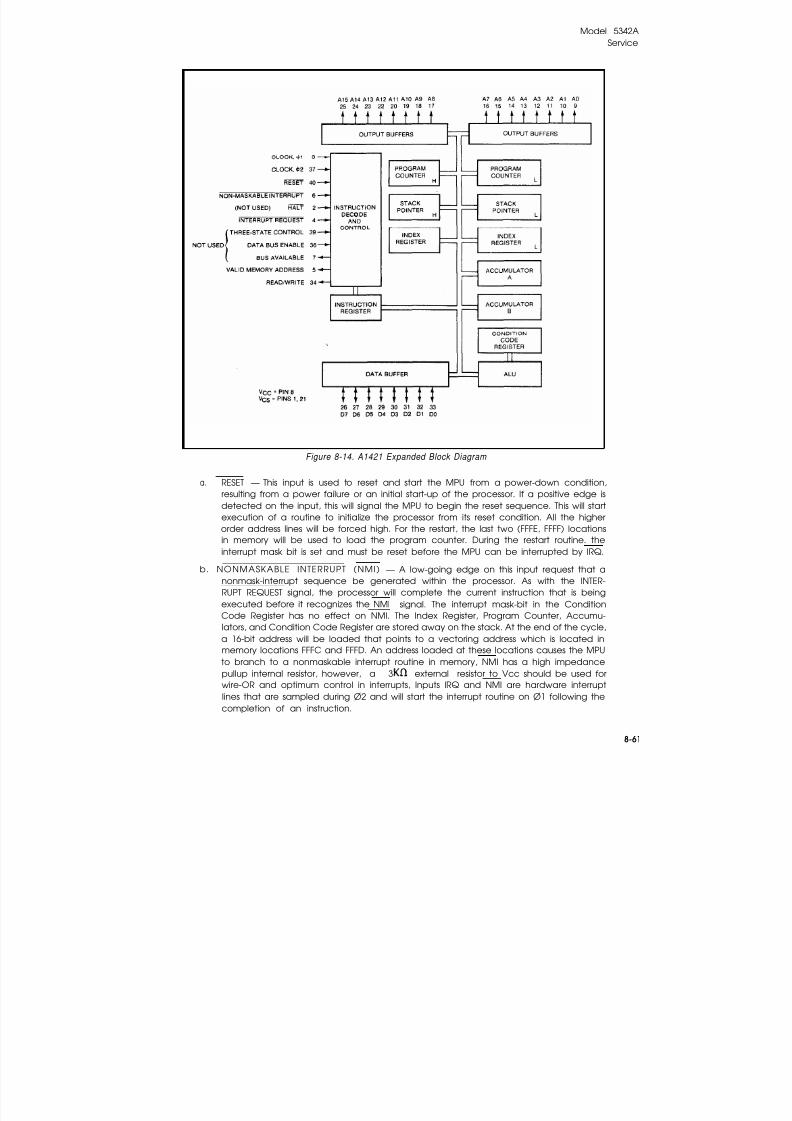
8/21/2019 HP5432 Microwave Frequency Counter
http://slidepdf.com/reader/full/hp5432-microwave-frequency-counter 221/364
Model 5342AService
Figure 8-14. A1421 Expanded Block Diagram
a. RESET — This input is used to reset and start the MPU from a power-down condition,resulting from a power failure or an initial start-up of the processor. If a positive edge isdetected on the input, this will signal the MPU to begin the reset sequence. This will startexecution of a routine to initialize the processor from its reset condition. All the higherorder address lines will be forced high. For the restart, the last two (FFFE, FFFF) locationsin memory will be used to load the program counter. During the restart routine. theinterrupt mask bit is set and must be reset before the MPU can be interrupted by IRQ.
b. NONMASKABLE INTERRUPT (NMI) — A low-going edge on this input request that anonmask-interrupt sequence be generated within the processor. As with the lNTER-RUPT REQUEST signal, the processor will complete the current instruction that is being
executed before it recognizes the NMI signal. The interrupt mask-bit in the ConditionCode Register has no effect on NMI. The Index Register, Program Counter, Accumu-lators, and Condition Code Register are stored away on the stack. At the end of the cycle,a 16-bit address will be loaded that points to a vectoring address which is located inmemory locations FFFC and FFFD. An address loaded at these locations causes the MPUto branch to a nonmaskable interrupt routine in memory, NMI has a high impedancepullup internal resistor, however, a 3 external resistor to Vcc should be used forwire-OR and optimum control in interrupts, Inputs lRQ and NMI are hardware interruptlines that are sampled during Ø2 and will start the interrupt routine on Ø1 following thecompletion of an instruction.
8-61
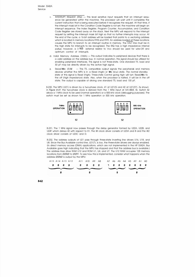
8/21/2019 HP5432 Microwave Frequency Counter
http://slidepdf.com/reader/full/hp5432-microwave-frequency-counter 222/364
8-62
Model 5342AService
c. INTERRUPT REQUEST (IRQ) — This level sensitive input requests that an interrupt sequ-ence be generated within the machine. The processor will wait until it completes thecurrent instruction that is being executed before it recognizes the request. At that time, ifthe interrupt mask bit in the Condition Code Register is not set, the machine will begin aninterrupt sequence. The Index Register, Program Counter, Accumulators, and ConditionCode Register are stored away on the stack. Next the MPU will respond to the interruptrequest by setting the interrupt mask bit high so that no further interrupts may occur. At
the end of the cycle, a 16-bit address will be loaded that points to a vectoring addresswhich is located in memory locations FFF8 and FFF9. An address loaded at these locationscauses the MPU to branch to an interrupt routine in memory. The HALT line must be inthe high state for interrupts to be recognized. The IRQ has a high impedance internalpullup; however, a 3 external resistor to Vcc should be used for wire-OR andoptimum control of interrupts.
d. Valid Memory Address (VMA) — This output indicates to peripheral devices that there isa valid address on the address bus. In normal operation, this signal should be utilized forenabling peripheral interfaces. This signal is not three-state. One standard TTL load and30 pF may be directly driven by this active high signal.
e. Read/Write (R/W) — This TTL compatible output signals the peripherals and memorydevices whether the MPU is in a Read (high) or Write (low) state. The normal standby
state of this signal is Read (high). Three-state Control going high will turn Read/Write tothe off (high impedance) state. Also, when the processor is halted, it will be in the offstate. The output is capable of driving one standard TTL load and 130 pF.
8-230. The MPU (U21) is driven by a two-phase clock, 41 at U21(3) and 42 at U21(37). As shownin Figure 8-37, the two-phase clock is derived from the 1 MHz input at XA14B(8, 8). Switch S2allows a 1 MHz clock to be used (normal operation) or a 500 kHz clock (debugging purposes). Theswitch must be set as shown for 1 MHz operation or 500 kHz operation.
8-231. The 1 MHz signal now passes through the delay generator formed by U22A, U22B, andU24F which delays 42 with respect to 01, The @l clock driver consists of U23A and B and the @2clock driver consists of U23C and D.
8-232, The address outputs of U21 pass through three-state inverting line drivers U16, U18, andU8. Since the Bus Available control line, U21(7), is Iow, the three-state drivers are always enabled.(In direct memory access (DMA) applications, which are not implemented in the HP 5342A, BusAvailable goes high indicating that the MPU has stopped and that the address bus is available.)
The address lines drive RAM U12 and ROM U1, U4, and U7. The U12 RAM occupies 128 memorylocations from ØØ8Ø to ØØFF. To see how this is implemented, consider what happens when theaddress ØØ8Ø is output by the MPU:
A15 A14 A13 A12 A11 A10 A9 A8 A7 A6 A5 A4 A3 A2 A1 A0

8/21/2019 HP5432 Microwave Frequency Counter
http://slidepdf.com/reader/full/hp5432-microwave-frequency-counter 223/364
Model 5342AService
After going through the inverting line drivers U16, U18, and U8, the address lines become:
A 1 5 A 1 4 A 1 3 A 1 2 A11 A10 A9 A8 A7 A6 A5 A4 A3 A2 A1 AØ
8-233. To address a location in RAM, all the enable inputs must be true. Consequently, U12(11)must be low, U12(12) must be low, U12(14) must be low, U12(10) must be high, U12(13) must behigh, and U12(15) must be low. The seven address inputs then select one of 128 locations in theRAM. For the case of ØØ8Ø sent out by the MPU, it is seen that U12(11) goes low when the inputs toU22D are both high (VMA high indicating that the address data on the address bus has settled andis valid data and Ø2 high); U12(12) is low since the inputs to U9B (inverted A15, A14, A13) are allhigh; U12(14) is low since the inputs to U9C (inverted A12, A11, A10) are all high; U12(10) is highsince the inputs to U5D are both high (inverted A9 and LFRERUN); U12(13) is high since invertedA8 is high; U12(15) is low since inverted A7 is low. Thus, due to the inversion, ØØ8Ø on the addressbus from the MPU accesses location ØØFF in RAM. In a similar fashion, memory assignments aremade to ROM U1 (78ØØ to 7FFF), ROM U4 (7ØØØ to 77FF), and ROM U7 (68ØØ to 6FFF).
8-234. The address lines are decoded by device decoding circuitry on A14. in some instances,
further decoding occurs at a particular device (for example, on the A13 Counter assembly). TheMPU treats an external device just like a memory location. To pass information between theregisters of the MPU and the registers of an external device (such as the count registers on the A13Counter assembly), the program writes or reads data from (or to) the location associated with thedevice. Address decoding circuitry decodes the address output from the MPU and generates astrobe which enables the register on the device. For example, to read data from the A1 keyboard,LKBRD goes low which enables the three-state bus driver A1U12 to drive the data bus and sendkeyboard information back to the MPU. The address location assigned to reading the keyboardis ØØ1Ø. When ØØ1Ø is output by the MPU, address decoding causes U20(7) to go low. Since onlyone device can drive the data bus at a time, all other device code outputs are high (so that thedevice buffers on these devices are in the high Z state). To see how ØØ1Ø causes U20(7) to go low,consider that the inverted address lines at the output of inverter buffers U16, U18, U8 will be:
A15 A14 A13 A12 A11 A10 A9 A8 A7 A6 A5 A4 A3 A2 A1 AØ
1 1 1 1 1 1 1 1 1 1 1 Ø 1 1 1 1
Since AØ, A1, and A2 are all high, these inputs to U20 will cause 7 to be decoded and U20(7) to golow provided that the control inputs U20(4) and U20(5) are both low. U20(5) goes low when theinputs to U22D are both high (VMA high and Ø2 high). U20(4) is low when U17 decodes theaddress output by the MPU and the address in the range of ØØ1Ø to ØØ17. U17(11) is low whenU17(14) is high and U17(13) is low, provided that the control input U17(15) is low. Since invertedA3 is high and inverted A4 is low, the U17(11) output will be low provided that U17(15) is low.U17(15) is Iow provided that U13A(2) and U13A(1) are both low. U13A(1) is Iow since inverted A5 ishigh. Inverted A15, A14, A13, A12, A11, A10 all high is decoded by U9A, U9B, and U13C. A9 is alsohigh. Thus U14 is enabled. Since inverted A8, A7, A6 are all high, the decoded 7 output U14(7)goes low. In summary, U14(7) goes low only when inverted A15, A14, A13, A12, A11, A10, A9,A8, A7, A6 are all high. Inverted A5 high, A4 low, A3 high is decoded by U17B. Inverted A2, A1,
and AØ all high is decoded by U20.
8-235. The eight bidirectional data bus lines coming out of U21 pass through an eight-sectionswitch, S1, which allows each line in the data bus to be opened for troubleshooting purposes.Resistor pack R6, with individual pull-up resistors connected to the data lines, together with twolines connected to ground via CR2 and CR3 (these lines connected to ground only whenLFRERUN is ground by switch S2), cause a CLB (clear accumulator B) instruction to be presentedto the MPU when the switch S1 is opened and LFRERUN is grounded. This causes the MPU tocontinuously increment the addresses on the address bus from the least significant address (ØØØØ)to the most significant address (FFFF) for diagnostic purposes when using the 5004A Signature
8-63

8/21/2019 HP5432 Microwave Frequency Counter
http://slidepdf.com/reader/full/hp5432-microwave-frequency-counter 224/364
Model 5342A
Service
Analyzer. LFRERUN grounded forces the Clear B instruction and also causes U15E(10) to go low
which disables RAM U12. With S1 opened, feedback is broken between the ROM outputs and
the MPU inputs which is a necessary condition for taking signatures with the HP 5004A Signature
Analyzer. If LXROM (Low External ROM) is grounded, the ROM’s U1, U4,and U7 will be disabled
by U6A(1) going low and the address lines can now be used to drive external memory residing in
the upper 32K of the memory map.
8-236. The power up reset circuitry formed by Schmitt trigger U11A, U11B, and inverter U15F
provides a low reset pulse to the MPU reset input U21(40) and a LDVRST output to the A2 DisplayDriver to blank the display during power-up. The length of the low reset is determined by the
time constant of resistors R5, R3, and capacitor C5 (400 milliseconds).
8-237. The LAMP EN input at XA14B(2) is used to indicate the presence or absence of the A16
Amplitude assembly (Option 002) since program execution will be different if this option is in-
stalled. If Option 002 is present in the HP 5342A, LAMP EN will be grounded. The LAMP EN line is
connected to three-state line driver U8 and the output connects to the D1 line of the data bus. To
check if Option 002 is present, the MPU sends out address 0018 which causes the output of
U11C(8) to go low and strobe a high (if LAMP EN is low) onto D1 of the data bus.
8-238. The eight data lines, after passing through switch S1, pass through bidirectional inverting
line drivers U3, U2. When data is being written out to the external devices (or to RAM), U21(34)
goes low which causes U12(16) to go low and U3(15), U2(15) to go high (and U3(1), U2(1) low)
thereby enabling the drivers which write to external devices. When data is being read from
external devices (or RAM), U21(34) goes high which causes U12(6) to go high and U3(1), U2(1)to
go low (and U3(15), U2(15) high). This enables the drivers in U2, U3, which read data from
external devices.
8-239. The memory assignments are summarized in Figure 8-15. Ordinarily, when power on, the
MPU executes the instructions in FFFF and FFFE. Since the A14 MPU assembly has the A15 address
line configured as “don’t care”, the MPU in the HP 5342A executes 7FFF and 7FFE after the power
on reset.
Figure 8-15. Memory Arrange me nt
8 - 6 4

8/21/2019 HP5432 Microwave Frequency Counter
http://slidepdf.com/reader/full/hp5432-microwave-frequency-counter 225/364
Model 5342AService
8-240. A15 OPTION 011 HP-IB ASSEMBLY
8-241. The A15 Option 011 HP-IB assembly is described under OPTIONS in paragraph 8-346.
8-242. A16 OPTION 002 AMPLITUDE MEASUREMENTS ASSEMBLY ANDA16 OPTION 003 EXTENDED DYNAMIC RANGE ASSEMBLY
8-243. The A16 Option 002 Amplitude Measurements assembly is described under OPTIONS inparagraph 8-296. The A16 Option 003 Extended Dynamic Range assembly is described in para-graph 8-331.
NOTE
The A16 slot is used for either the Option 002 or 003pc assembly. Only one of these options can be in-stalled in an instrument.
8-244. A17 TIMING GENERATOR ASSEMBLY
8-245. The A17 Timing Generator shown in Figure 8-41 has the following functions: duringacquisition, it generates the pseudorandom sequence used to switch the A5 Multiplexer and the
A13 counters for N determination; after acquisition, it generates gate times for the measurementof the IF on A13; between measurements, its sample rate circuitry determines when to begin anew measurement.
8-246. The DØ through D5 data lines from the microprocessor data bus transmit data from themicroprocessor to the hex D-type register U19 when the LTIMWRT signal (decoded on A14) goeslow. LTIMWRT returning high clocks the data into the register. The data lines also transmit databack to the microprocessor from hex three-state driver U18 which drives the data bus whenLTIMRD (decoded on A14) goes low.
8-247. Pseudorandom Sequence Generation
8-248. During acquisition, after a countable signal has been detected and the sweep stopped,
the N number must be computed. By measuring the IF1 frequency which occurs when the Nthharmonic of the main VCO mixes with the unknown frequency and then measuring the IF 2 thatoccurs when the Nth harmonic of the offset VCO mixes with the unknown, the harmonicnumber N can be determined. N equals (IF1-IF2)/500 kHz where 500 kHz is the precise fre-quency difference between the main VCO and the offset VCO. To speed the process of deter-mining N, two counters (on A13) are used, counter A and counter B. To prevent coherence be-tween FM on the unknown signal and the switching rate between counters from causing an in-correct computation of N, the switching between counter A and B (which is synchronous with theswitching in A5 between the main VCO and the offset VCO) is done in a pseudorandom fashion.Two different sequence lengths are possible: 1) the normal or short pseudorandom sequence(prs) which lasts for a total time of 360.4 milliseconds (counter A and counter B are open for 163.83ms each — there’s ~32.8 ms of “dead” time). This short prs gives a worst case FM tolerance of20 MHz peak-to-peak; or 2) the long prs, which is selected by a rear panel switch, lasts for a total
time of 2.096 seconds (counter A and counter B are open for 524 ms each in addition to 1.048seconds of “dead” time). This long prs gives FM tolerance of 50 MHz peak-to-peak.
8-249. To begin the pseudorandom sequence, the microprocessor writes to A17 and setsU19(15) high (prs enable), U19(12) low (gate time disable), U19(7) high (for 1 MHz prs clock), andU19(5) high for the long prs or sets U19(2) high for the normal prs. For the short prs, a 100 kHz prsclock is used and U19(7) is low. Decade divider U11 divides down the 1 MHz input to 100 kHzwhich appears at U10(8). For the long prs, a 1 MHz prs clock is used and U19(7) is high. SinceU11(1, 3) are both high, the counter is preset to 9 so that U11(9, 8) are both high whichenables U10. Thus the 1 MHz input appears at U10(8) and becomes the prs clock.
8-65

8/21/2019 HP5432 Microwave Frequency Counter
http://slidepdf.com/reader/full/hp5432-microwave-frequency-counter 226/364
Model 5342A
Service
8-250. The prs generator consists of shift registers U7, U4, U5, 4-bit counters U2, U1, and logicgates U6, U3. When U19(15) (prs enable) goes high, the output of U14(11) goes high whichreleases the reset signal from all the components of the prs generator and starts the sequence.To generate the sequence, data is shifted through the shift register formed by U5, U4, and U7.Feedback taps exclusively “OR” two of the shift register outputs to generate the next input. This
feedback generates the prs. For the short prs, U3B(4) is high and U6A is used to perform theexclusive “OR” function (the output of U7(6) is not used for the short prs), For the long prs,
U3A(1) is high and U6B performs the exclusive “OR”. The data is then fed back to the input of theshift register at US(1, 2) via inverter U3C.
8-251. The short prs is 15 bits long and stops after 14 consecutive highs in the sequence aredetected. The long prs is 20 bits long and stops after 19 consecutive highs in the sequence are de-tected. The detection of the number of consecutive highs in the sequence is performed by pre-settable counters U2 and U1. For the short prs, “1” is preset into U2 (least significant counter) and“15” is preset into U1 (most significant counter) by a low level on U2(9) and U1(9). When a highappears in the sequence, the U2 counter is incremented by the prs clock at U2(2). When a lowappears in the sequence, U2 and U1 are reset to the initial preset conditions and counting upbegins again. After 14 consecutive highs in the prs, U2 has counted to “15" and the carry outputU2(15) has enabled U1 so that the 14th clock causes the carry output U1(15) to go high. This causesU8A(3) to go low which resets the latch formed by U14A and U14B so that U14D(11) goes low to
reset U7, U4, U5, U2, and U1.
8-252. For the long prs, operation is similar: this time “12” is preset in U2 and “14” is preset intoU1 so that after 19 consecutive 1’s in the prs, the carry out of U1 sets U14A(3) Iow so that U14D(11)is low and clears the prs generator.
8-253. To allow sufficient settling time for the multiplexer on A5 after switching, 2 microsecondsof dead time are added to each transition in the sequence which means that the transitions ofthe LIF GATE signal (which enables counter A or counter B on A13) are delayed with respect tothe LO Switch signal which switches the A5 multiplexer and switches between counter A andcounter B on A13 as shown below:
8-254. The dead time in the LIF GATE signal is generated by D flip-flops U9A, U9B, exclusive“OR” U6D, and D flip-flop U15A. The dead time is generated when U6D(11) goes high for twoperiods of the 1 MHz clock. With U6D(11), high, U10B is disabled and the prs clock at U10C(8)remains high. The reset input to U15A(1) is low during the prs generation so that U15A(5) is low.When the preset input U15A(4) goes low also, the output goes high for the time that the preset
8-66
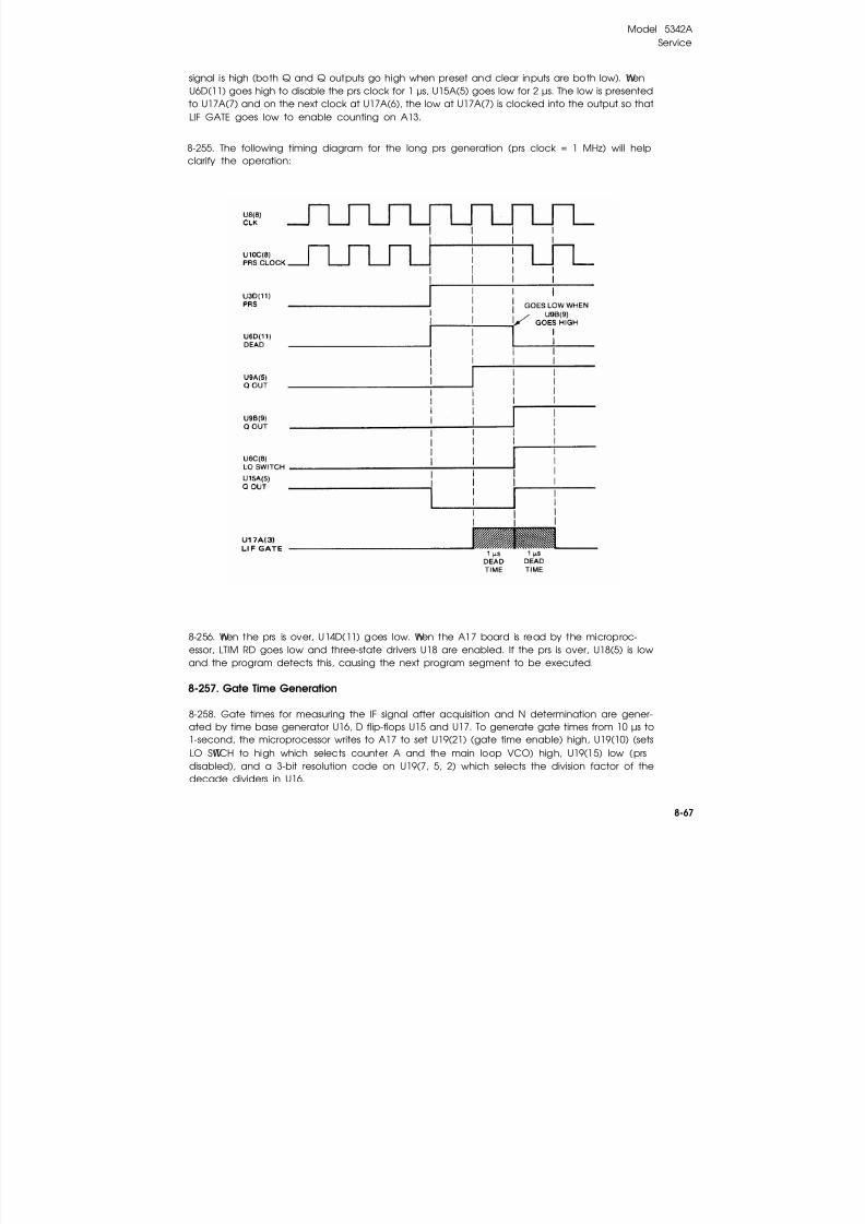
8/21/2019 HP5432 Microwave Frequency Counter
http://slidepdf.com/reader/full/hp5432-microwave-frequency-counter 227/364
Model 5342AService
signal is high (both Q and Q outputs go high when preset and clear inputs are both low). WhenU6D(11) goes high to disable the prs clock for 1 µs, U15A(5) goes low for 2 µs. The low is presentedto U17A(7) and on the next clock at U17A(6), the low at U17A(7) is clocked into the output so thatLIF GATE goes low to enable counting on A13.
8-255. The following timing diagram for the long prs generation (prs clock = 1 MHz) will help
clarify the operation:
8-256. When the prs is over, U14D(11) goes low. When the A17 board is read by the microproc-essor, LTIM RD goes low and three-state drivers U18 are enabled. If the prs is over, U18(5) is low
and the program detects this, causing the next program segment to be executed.
8-257. Gate Time Generation
8-258. Gate times for measuring the IF signal after acquisition and N determination are gener-ated by time base generator U16, D flip-flops U15 and U17. To generate gate times from 10 µs to1-second, the microprocessor writes to A17 to set U19(21) (gate time enable) high, U19(10) (setsLO SWITCH to high which selects counter A and the main loop VCO) high, U19(15) low (prsdisabled), and a 3-bit resolution code on U19(7, 5, 2) which selects the division factor of thedecade dividers in U16.
8-67
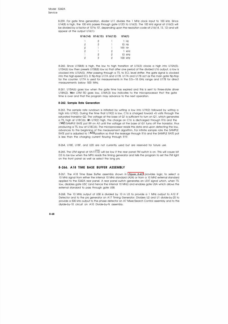
8/21/2019 HP5432 Microwave Frequency Counter
http://slidepdf.com/reader/full/hp5432-microwave-frequency-counter 228/364
Model 5342AService
8-259. For gate time generation, divider U11 divides the 1 MHz clock input to 100 kHz. SinceU14(8) is high, the 100 kHz passes through gate U12D to U16(3). The 100 kHz signal at U16(3) willbe divided by a factor of 100 to 105, depending upon the resolution code at U16(14, 13, 12) and willappear at the output U16(1):
U 16(14) U16( 13) U 16(12) U16(1)
1 Ø 1 1 Hz
Ø Ø 1 10 HzØ 1 1 100 HzØ 1 Ø 1 kHz1 Ø Ø 10 kHzØ Ø Ø 100 kHz
8-260. Since U15B(8) is high, the low to high transition at U15(3) clocks a high into U15A(5).U15A(6) low then presets U15B(8) low so that after one period of the divided U16 output, a low isclocked into U15A(5). After passing through a TTL to ECL level shifter, the gate signal is clockedinto the high-speed ECL D flip-flop U17A and U17B. U17A and U17B act as the main gate flip-flopfor the counter. U17A is used for measurements in the 0.5—18 GHz range and U17B for directmeasurements below 500 MHz.
8-261. U15A(6) goes low when the gate time has expired and this is sent to three-state driverU18A(2). When LTIM RD goes low, U18A(3) low indicates to the microprocessor that the gatetime is over and that the program may advance to the next operation.
8-262. Sample Rate Generation
8-263, The sample rate rundown is initiated by writing a low into U19(2) followed by writing ahigh into U19(2). During the time that U19(2) is low, C16 is charged toward +5 volts through thesaturated transistor Q2. The voltage at the base of Q1 is sufficient to turn on Q1, which generatesa TTL high at U18C(6), With U19(2) high, the charge on C16 is discharged through R16 and the1 SAMPLE RATE pot R9 on A2 until the voltage at the base of Q1 turns off the transistor, thusproducing a TTL low at U18C(6). The microprocessor reads this data and upon detecting the low,advances to the beginning of the measurement algorithm, For infinite sample rate the SAMPLERATE pot is adjusted to 1 position so that the leakage through R16 and the SAMPLE RATE potis less than the charging current flowing through R19.
8-264, U18E, U18F, and U20 are not currently used but are reserved for future use.
8-265, The LFM signal at XA17(12) will be low if the rear panel FM switch is on. This will cause bitD3 to be low when the MPU reads the timing generator and tells the program to set the FM lighton the front panel as well as select the long prs.
8-266. A18 TIME BASE BUFFER ASSEMBLY
8-267. The A18 Time Base Buffer assembly shown in Figure 8-42, provides logic to select a10 MHz signal from either the internal 10 MHz standard (A24) or from a 10 MHZ external standardapplied to the 5342A rear panel. A rear panel switch generates an LEXT signal which, when TTLlow, disables gate U5C (and hence the internal 10 MHz) and enables gate U5A which allows theexternal standard to pass through gate U5B.
8-268. The 10 MHz output of U5B is divided by 10 in U3 to provide a 1 MHz output to A12 IFDetector and to the prs generator on A17 Timing Generator. Dividers U2 and U1 divide-by-20 toprovide a 500 kHz output to the phase detector on A7 Mixer/Search Control assembly and to thediyide-by-10 circuit on A10 Divide-by-N assembly.
8-68

8/21/2019 HP5432 Microwave Frequency Counter
http://slidepdf.com/reader/full/hp5432-microwave-frequency-counter 229/364
8-69
Model 5342AService
8-269. A19, A20, A21 POWER SUPPLY
8-270. The power supply used in the 5342A is a high efficiency switching regulator whichis made up of the A19 Primary Power Assembly, the A20 Secondary Power Assembly, and theA21 Switch Drive Assembly. The ac line voltage is directly rectified on A19. Consequently,A19 is isolated from the rest of the instrument and care must be exercised when voltage mea-surements are made on A19. A19 measurements should be made by supplying power to the
5342A via an isolation transformer.
8-271. SIMPLIFIED BLOCK DIAGRAM. Figure 8-16 is a simplified block diagram of the 5342Apower supply. As shown in the diagram, the supply consists of six major elements: an inputrectifier-filter, a pair of push-pull switching transistors (A19Q1, Q2), an RF transformer(A20T1), output rectifiers and associated linear voltage regulators, a pulse width control feed-back network, and current limiting circuitry.
8-272. VOLTAGE REGULATION LOOP. Regulation is accomplished primarily by switchingtransistors Q1 and Q2 under control of a feedback network consisting of the A21U4 20 kHzoscillator/pulse width modulator, and the switch drive transformers on A19. The schematic
diagram is shown in Figure 8-43. If the 5V (D) output (digital supply) voltage attempts to de-crease, the +5V sense signal drops which causes an error signal (difference between +5V senseand +5V reference set by A21R17) to drive a pulse width modulator (part of U4) and increasethe pulse width of the 20 kHz outputs of A21U4. Conversely, for an increase in the voltage of+5V (D), the pulse width of the A21U4 outputs decrease. The net result of controlling the pulsewidth of the 20 kHz output is to control the duty cycle of the output waveforms of Q1, Q2, andhence the duty cycle of the rectangular waveform delivered to the LC filter in the +5V (D)output. The LC filter averages this rectangular waveform to produce a dc output level whichis proportional to the duty cycle of the input waveform.
8-273. The feedback provided by the +5V (D) sense signal establishes a controlled input tothe primary of A20T1. Other taps on the secondary of A20T1 are rectified, filtered, and de-
livered to individual linear voltage regulators to provide +5V (A) output (analog supply), -5.2V,+15V, -15V, and +12V.
8-274. The oven transformer output is rectified and filtered to provide power to the controlcircuits U3, U4 on A21 and oven power when the Option 001 oven oscillator is installed. Theseoven transformer voltages are available whenever the 5342A is plugged into the line voltage,regardless of the position of front panel power switch.
8-275. CURRENT LIMITING. Total current load is sensed by resistor A19R5 and a signal issent, via, optical isolator CR2, to the A21U3 Timer which acts as an overcurrent shutdown cir-cuit. When excessive current is drawn, the output of U3 turns off the 20 kHz oscillator on U4for approximately 2 seconds.
8-276. For output voltages other than the +5V (D) output, excessive current may or may notcause A21U4 to turn off since the current limiting circuitry built into the individual linear regu-Iaor may shutdown the output before the U3 Timer has time to shutdown the 20 kHz oscil-lator in U4.
8-277. When the hold-off output of U3 is TTL high, the 20 kHz oscillator on U4 i s disabled.This high level causes a red LED to light which indicates overcurrent shutdown. When thisoccurs, the green LED on A20 turns off, indicating the absence of +5V (D).

8/21/2019 HP5432 Microwave Frequency Counter
http://slidepdf.com/reader/full/hp5432-microwave-frequency-counter 230/364
8
7
F i g ur e 8 -1 6 .A 1 9 ,A 2 0 , an d A 2 7
P ow er S u p pl y B l o c k D i a gr am

8/21/2019 HP5432 Microwave Frequency Counter
http://slidepdf.com/reader/full/hp5432-microwave-frequency-counter 231/364
Model 5342AService
8-278. A22 MOTHERBOARD
8-279. The A22 Motherboard contains the XA (Assembly No.) connectors for the plug-inprinted circuit assemblies (cards) and provides interconnections between the cards. Themotherboard also contains terminals and connectors for interconnection of assemblies tothe front and rear panels.
8-280. A23 POWER MODULE
8-281. The A23 Power Module is mounted on the rear panel of the 5342A and contains aconnector for a power cable, a fuse and a pc card. The pc card can be inserted in any one offour positions to select 100-, 120-, 200-, or 240-volt ac operation. The schematic diagram of thepower module is shown in Figure 8-43 and a detailed description is contained in paragraph 2-6.
8-282. A24 OSCILLATOR ASSEMBLY
8-283. The A24 oscillator board contains a 10 MHz crystal oscillator that supplies the internalsignal to the A18 Time Base Buffer Assembly. An Option 001 A24 board contains an oven-controlled crystal oscillator (10544A) that results in higher accuracy and longer time periodsbetween calibration. Refer to the specification listed in Table 1-1. The schematic diagrams for
both oscillators is shown in Figure 8-44.
8-284. A25 PREAMPLIFIER
8-285. The A25 Preamplifier Assembly shown in Figure 8-45, combines the two outputs fromthe sampling diodes in the U1 Sampler and provides approximately 42 dB gain for the sampleroutput. This gain remains approximately flat out to 125 MHz and rolls off by 8 to 10 dB at 175MHz. This roll-off for frequencies above 125 MHz prevents interference between the differ-ence frequency produced by the desired Nth harmonic of the VCO mixing with the unknownand the difference frequency produced by the (N±1) harmonic of the VCO mixing with theunknown. Refer to paragraph 8-105 for a detailed description of sensitivity.
8-286. A level detecting diode (CR1) detects RF level and is used to indicate overload to the
microprocessor. The detected RF output is also used for controlling current sources on A25which are used to control pin diode attenuators in the Amplitude Option (002) and ExtendedDynamic Range Option (003).
8-287. The two sampler outputs are combined in C5 and C9 at the input and are passed tothe first stage of amplification. High frequency transistor Q22 and its associated circuitry pro-vide approximately 10 dB gain. Resistors R6 and R7 provide negative feedback to stabilizeQ2’s operating point. Emitter resistors R14 and R13 are low inductance strip resistors and alsoprovide negative feedback for gain stabilization. The amplified output of Q2 is coupledthrough dc blocking capacitor C7 to a similar stage of amplification built around Q1. Theoutput of this second stage is approximately 24 dB greater than the input from the samplerand is coupled through C8 to a 3 dB pad, consisting of R9, R17, and R16, which provides a welldefined driving impedance for all subsequent filter and amplifier stages. The signal then
passes through an elliptic function filter consisting of L3, L4, L6, C10, L5, L7, and C11. This filterreduces the 500 MHz bandwidth of the first two stages to something less than 175 MHz.Variable capacitor C11 is adjusted to provide the required roll-off at 175 MHz. Differentialpair U1 provides approximately 14 dB gain.
8-288. The output of U1 passes through a 200 MHz low-pass filter whose major purpose is tofilter out the fundamental sampling frequencies of the main oscillator and offset oscillatorwhich appear in the output of the sampler. Differential pair U2 provides another 14 dB gainand the output is coupled through capacitor C26 to the A11 IF Limiter Assembly.
8-71

8/21/2019 HP5432 Microwave Frequency Counter
http://slidepdf.com/reader/full/hp5432-microwave-frequency-counter 232/364
Model 5342AService
8-289.which
Diode CR1 rectifies the output of the 175 MHz elliptic filter and provides an outputis proportional to the amplitude of the RF input signal. This level is fed to voltage com-
parator U3, which, due to the positive feedback provided by R33, has hysteresis and operateslike a Schmitt trigger. When the dc level from the detecting diode CR1 rises above the levelat U3(2), set by “OFST” potentiometer R31, the output of U3 goes TTL high which causesU4(3) to go low. This output, called LOVL, is sent to the A12 IF Detector where it is bufferedand read by the microprocessor. If LOVL is low, then the microprocessor sends dashes to the
counter display. Potentiometer R31 is adjusted so that LOVL goes low when the RF into thecounter exceeds about +5 dBm. When U4A(3) goes low due to the RF input level exceeding+5 dBm, the RS latch formed by U4B and U4D is set so that U4B(6) is TTL high. This causesU4C(8) to go low which turns off transistor Q4. With Q4 turned off, the voltage at the base ofQ5 goes to +15 volts and Q5 is turned off. The current source formed by Q6, R41, R39, CR5,and R40 is always on. By turning off the current source formed by Q5 and R36, the currentflowing through the pin diode attenuator (Options 002, 003 only) is decreased and the dioderesistance increases by approximately 15 dB. This allows signals up to approximately +20 dBmto be measured if Option 002 or 003 is present. For signals less than +5 dBm U4C(8) is high, Q4is on and the Q5 current source is on. Since more current flows through the pin diode, its re-sistance is less (by 15 dB). A LPWR ST signal from A11 resets the RS latch U4B, D when the inputpower level drops below about -15 dBm.
8-290. A26 SAMPLER DRIVER ASSEMBLY
8-291. The A26 Sampler Driver shown in Figure 8-46 converts the LO FREQ sine wave signalinto a negative spike waveform at the same frequency as the LO FREQ signal input. The spikegoes from +0.7V dc to about -8V dc with a slew rate of approximately 8 picoseconds/volt. Thisfast transition is used to turn on the sampling diodes in the sampler for a few picoseconds andis necessary in order to produce useable harmonics of the VCO frequency up beyond 18 GHz.
8-292. The input frequency, in the range of 300 to 350 MHz, is applied to a common collec-tor amplifier formed by one-half of transistor pair U1 (ac coupling for the LO FREQ signal isprovided on the A5 RF Multiplexer). The otuput is taken off the emitter of the 1st transistor,
through R5, and is applied to the common emitter formed by the other half of U1. Matchingnetwork R1, L1, C3, L3, L2, C1 is used to match the output impedance of U1 to the step re-covery diode CR1.
8-293. AGC is provided by coupling part of the U1 output through CR5 to detecting diodeCR2. The detected dc voltage which appears across C10 is used to cause transistor Q1 to con-duct more or less current, thereby changing the gain through the first transistor in U1. Thegain is changed in such a fashion as to cause the A26 output at the SMA connector A26J1 tohave little change in amplitude for variations in input signal amplitude. The output is sent toU1 Sampler.
8-294. OPTIONS THEORY (OPTIONS 002, 003, 004, AND 011)8-295. The following paragraphs contain thefollows:
a. Option 002 Amplitude Measurements
b. Option 003 Extended Dynamic Range
theory of operation for the 5342A options as
c. Option 004 Digital-to-Analog Conversion (DAC)
d. Option 011 Hewlett-Packard Interface Bus (HP-IB)
8-72
8/21/2019 HP5432 Microwave Frequency Counter
http://slidepdf.com/reader/full/hp5432-microwave-frequency-counter 233/364
Model 5342AService
8-296. OPTION 002 AMPLITUDE
8-297. Introduction
MEASUREMENTS OVERALL THEORY
8-298. The 5342A measures amplitude by multiplexing the counter input signal (either at the0.5 to 18 GHz high-frequency input or 10 Hz to 500 MHz low-frequency input) between thenormal counting circuits and the amplitude measuring circuits. An amplitude measurement
takes approximately 100 milliseconds.
8-299. The multiplexing is performed by the U2 High Frequency Amplitude Assembly forthe 0.5 to 18 GHz input or by the A27 Low Frequency Amplitude Assembly for the direct countinput (when the 50fl - lMf2 switch is in the 500 position). The A16 Amplitude Assembly com-pletes the assemblies required for amplitude measurements.
8-300. Block Diagram
8-301. Figure 8-17 is a simplified block diagram of the amplitude measurement option. Theincoming 0.5 to 18 GHz rf signal is applied to the rf detector diode inside the U2 assembly.Since the transfer function of the detector diode changes with input level and temperature,
a feedback circuit using two diodes in thermal proximity is used. The feedback circuit linear-izes the transfer characteristic between the rf input voltage and the dc voltage output to theanalog to digital converter and compensates for the temperature drift of the detector diode.
8-302. The rf detector is driven by the input signal and the 100 kHz detector is driven by avariable amplitude 100 kHz signal generated on the A16 Amplitude Assembly. The feedbackloop adjusts the amplitude of the 100 kHz signal so that the output of the 100 kHz detector isequal to the output of the RF detector. The amplitude of the 100 kHz signal is determined, logconverted, corrected by calibration data stored in PROM, and is output to the display as theamplitude of the rf input signal in dBm.
8-303. The amplitude of the 100 kHz signal is determined by measuring (with an analog todigital converter) the dc control voltage which determines the amplitude of the 100 kHz signal.
The dc control voltage, which is developed by the error amplifier, drives a linear modulatorwhich varies the amplitude of the 100 kHz signal. The proportionality constant between controlvoltage input and the amplitude of the 100 kHz output is known and is used by the programresiding in ROM to compute the level of the 100 kHz signal.
8-304. Further linearization of the diode characterization is provided by a programmableROM which is specifically programmed to compensate for a particular U2 assembly. Thus, thePROM and U2 assembly form a matched pair unique to each instrument with option 002.
8-305. OPTION 002 DETAILED THEORY
8-306. U2 High Frequency Amplitude Assembly (5088-7035)
8-307. The U2 assembly is a thin film hybrid circuit built on a sapphire substrate and placed ina hermetically sealed package. It is not field repairable. This assembly is the microwave frontend which switches the microwave input signal between the U1 Sampler for frequency mea-surements and the U2 detectors for amplitude measurements. It also can provide approximately15 dB attenuation to the signal which is routed to the U1 Sampler,
8-308. The microwave signal enters at U2J1, as shown in Figure 8-39, and passes through dcblocking capacitor Cl. PIN diodes CR1 and CR2 switch the signal either to the U1 sampler orthe U2CR3 Shottky diode detector. A positive signal at the FREQ on input (approximately 2.5volts and 30 mA when “on” and approximately +0.7 volts when “off”) turns on CR1 and routes
8-73

8/21/2019 HP5432 Microwave Frequency Counter
http://slidepdf.com/reader/full/hp5432-microwave-frequency-counter 234/364
F i g ur e 8 -1 7 . O p t i on 0 0 2 A m pl i t u d eM e a s ur em en t s B l o c k D i a gr am
8 -7 4

8/21/2019 HP5432 Microwave Frequency Counter
http://slidepdf.com/reader/full/hp5432-microwave-frequency-counter 235/364
Model 5342AService
the microwave signal to U212 RF OUT (CR2 is off since the AMPL ON signal is at +0.7 volts). Apositive signal at the AMPL ON input (approximately +2.5 volts) turns on CR2 and routes thesignal to detector CR3 CR1 is off in this model. The detected microwave signal, DETECTEDRF (HF), exists through feedthrough capacitor C10. This dc level can vary from -500 µV (for inputsaround -30 dBm) up to -2 volts (for +20 dBm inputs).
8-309. The 100 kHz (HF) input from A16 is detected by Shottky diode CR4 which is in thermal
proximity to CR3. The DETECTED 100 kHz (HF) output is sent to A16 for comparison with thedetected microwave signal.
8-310. A27 Low Frequency Amplitude Assembly
8-311. This assembly, shown in Figure 8-39, performs the same function as the U2 assemblyby switching the input signal (in the range of 10-520 MHz) between the A3 Direct Count Ampli-fier for frequency measurements and A27CR3 Shottky diode detector for amplitude measure-ments. The frequency range for amplitude does not go below 10 MHz due to the storage timeof the PIN diodes.
8-312. When the AMPL. SEL. input is +15 volts, CR1 is turned on via R4 to ground and CR2 isturned off. This routes the input signal to A3 for frequency measurements. When AMPL SEL is-15 volts, CR2. is turned on via R3 to ground and CR1 is turned off.This routes the input to Shottkydiode detector CR3.
8-313. Detector CR4 detects the 100 kHz input and the detected output is sent to A16 for com-parison with the detected low frequency signal. Variable resistors R9 and R10 are used to com-pensate for differences between matched. detector diodes CR3 and CR4 j and the insertion lossof the PIN diode switch
8-314. A16 Amplitude-Assembly
8-315. The A16 Amplitude Assembly, shown in Figure 8-39, consists of the analog feedbackloop, the analog to digital converter (which digitizes the dc output voltage from the feedback
loop), the- switching circuitry required for the U2 and A27 assemblies, and the digital circuitryincluding the: U4- ROM containing the amplitude measuring algorithm.
8-316. ANALOG LOOP, The analog feedback loop consists of U18 differential error amplifier,U14; transistors Q10, Q11, Q12 and associated circuitry for generating the 100 kHz feedback.signal, range amplifier U12 switch U17 and relay K1.
8-317. The LDIRECT signal sent to transistor Q13 from Counter Assembly A13 is set low by themicroprocessor if the front panel RANGE switch (read by the microprocessor from A2U12, pin 9)is in the 10 Hz-500 MHz position. LDIRECT low causes relay K1 and bilateral switch U17 to con-nect the A27 low frequency module. 100 kHz input and the two detector outputs to the A16cicuits. LDIRECT high causes the U2. multiplexer inputs and outputs to be-connected to theA 16 circuits. Since the front end is being switched between frequency measurements and ampli-
tude measurements, the output of either detector appears as a negative pulse train. To pre-vent switching the front end during troubleshooting, use diagnostic mode 5 or 6. Diagnosticmodes are described in Table 8-8.
8-318. Consider circuit operation for the case where the front panel RANGE switch is in the0.5 to 18 GHz position. In this case, the DETECTED RF (HF) signal from U2 is connected to theinverting input of U18 and the DETECTED 100 kHz (HF) signal from U2 is connected to the non-inverting input of U18. The 100 kHz (HF) input is connected through U18 and associated circuitsto buffer U15. The dc voltage difference between-the detected 100 kHz signal and the detectedmicrowave signal is amplified by U18. However, the negative feedback of the loop causes the
8-75

8/21/2019 HP5432 Microwave Frequency Counter
http://slidepdf.com/reader/full/hp5432-microwave-frequency-counter 236/364
Model 5342A
Service
difference between the detected RF and detected 100 kHz to be very small. Although the volt-age difference is amplified by the very high gain of U18, the U18 output voltage stays within thedynamic range of U18 because the difference is extremely small. When a frequency measure-ment is being made, the output of U18 is shorted to its input by switch U1312,3) to prevent U18from saturating.) The output of U18 drives U14 which converts the input voltage to a current bydriving Q11. The current flowing through Q11 sets the gain of differential pair Q10, Q12 andthis gain is directly proportional to the Q11 current. The 1 MHz input to A16 is applied to decadedivider U10 and the 100 kHz output is amplified by differential pair Q10, Q12. The output ofQ10, Q12 is filtered by the 100 kHz active filter U16 to produce a 100 kHz sinewave. Since thissignal must drive 50 ohms on the U2 assembly (or A27assembly), it first passes through bufferdriver U15. The gain of the loop is adjusted by resistor R29.
8-319. The voltage at the input to U14(3) is directly proportional to the amplitude of the micro-wave signal since the voltage at U14(3) determines the amplitude of the 100 kHz signal. The volt-age at U12(3) is equal to the voltage at U14(3) due to the feedback around U14. Amplifier U12amplifies this voltage by X1 (for input levels above about -2 dBm) or by X16 (low range for levelsbelow about -2 dBm). The gain of U12 is controlled by Low Range bilateral switch U13 which iscontrolled by the LLRNG bit output of U5(14). If U5(14) is low, then U12 amplifies by X16 [U13(7, 6)open and U13(I0, 11) closed]. If U5(14) is high, then U12 amplifies by X1 [13(7, 6) closed, andU13(10, 11) open]. Any dc offset in the loop and in U12 is corrected by adjusting resistor R26.
8-320. U8 ANALOG TO DIGITAL CONVERTER. The output of U12 feeds the U8 analog todigital converter which converts the dc voltage at U8(5) to a 13-bit, 2’s complement, digital word.
The microprocessor, after detecting the end of the A to D conversion, reads the digital word intwo 8-bit bytes. The input power is computed and displayed. ROM U4- contains the firmwaresubroutine which controls the amplitude measurement process and PROM U3 contains thecorrections for frequency (as. measured by the counter) and level (as measured by the U8 Analogto Digital Converter).
8-323. Register U5 is used by the microprocessor to write to the A16 Amplitude Assembly.U1(10) clocks the data on the data lines into U5 when the LAMP MTR signal is low and the LR/HWsignal goes low to high.
8-322. U5(3) contains the START CONVERSION input to U8. When START, CONVERSIONgo-high, U8’S digital logic is initialized and BUSY is latched high. When START Conversionreturns low, the conversion begins.
8-323. U5(6) controls the HIGH BYTE ENABLE. (HBEN) input of U8 and the-STATUS ENABLE(STEN) input of U8. When HBEN is high, the high order data bits (five most significant bits) appearat U8(29, 30, 31,32, 33). HBEN low causes these outputs to float (high Z state). STEN high enablesthe status bits BUSY, and OVERRANGE (OVRG). BUSY indicates conversion complete.The microprocessor waits 40 ms after the START pulse and then continually reads the BUSY bitU8(36) until the bit is low (conversion complete). if conversion complete does not occur within140 ms, error message E16.1 is displayed. When U8(36) is high, the conversion is in progress(approximately 40 ins), The overrange bit, OVRG, at U8(34) goes high if the input voltage hasexceeded the plus or minus full scale voltage by at least 1/2 LSB.
8-324. Register US(7) controls the Low Byte Enable (LBEN) input of U8. When LBEN is high, thelow order data bits (eight least significant bits) appear at U8(21, 22,23,24, 25, 26,27, 28). LBEN lowcauses these outputs to float. After the microprocessor determines that the conversion is over,the high order bits are read and then the low order bits are read.
8-325. Muitiplexers U6 and U7 are used to switch between the output of U8 and the output ofPROM U4. When U2(4) goes low, the three-state outputs of U6 and U7 are enabled. U2(4) goeslow when LAMP MTR and LR/HWare both low or when U1(2) goes high, U1(2) goes high whenthe correction data in PROM U4 is being read. The signal at U6(1) and U7(1) determines which
8-76

8/21/2019 HP5432 Microwave Frequency Counter
http://slidepdf.com/reader/full/hp5432-microwave-frequency-counter 237/364
Model 5342AService
output will be read by the microprocessor. If U2(5) is high, then the U8 ADC outputs are selectedU6(3, 6, 13, 10) and U7(3, 6, 13, 10). If U2(5) is low, then the U4 PROM outputs are selected. Theoutput of U8 is first read by the microprocessor by having U6, 7(1) high. Then U6, 7(1) goes lowand the correction is read from U4 for that particular frequency and level.
8-326. MULTIPLEX CONTROL. Transistors Q1 through Q9 and associated circuitry are respon-sible for controlling the rf signal multiplexing in U2 and A27. In addition, this circuitry controls
the attenuation of the pin diode U2 CR1 to allow 0.5 to 18 GHz frequency measurements atlevels to +20 dBm.
8-327. When a frequency measurement is made, the microprocessor sets U5(10) high whichnot ony closes switch U13(2, 3) but also turns on transistor Q8 and Q7. With the collector of Q7near +15V, Q5 is turned on and Q3 is turned off. The emitter of Q3, which is the Amplitude Select(AMPL SEL) signal sent to A27, will be near +15 volts, thereby routing the low frequency inputsignal to the A3 Direct Count Assembly for a frequency measurement. With U5(10) low, Q8 andQ7 are off. The base of Q5 and Q3 is pulled toward -15 volts, which turns off Q5 and turns on Q3.The emitter of Q3 drops to near -15V which causes A27 to route the low frequency input signalto the A27CR3 detector for an amplitude measurement.
8-328. Consider what happens at the same time for the U2 Assembly. For amplitude measure-
ments, U5(10) is low and U5(11) is high. U5(11) high turns on Q6. Since there is no signal into thesampler, the current source on A25 is sourcing high current (approximately 30 mA), via the AT1signal input, to the collector of Q6. Since Q6 is on, this current does not greatly raise the voltageat the base of Q9 so that Q9 is on, applying approximately +2.5 volts to the AMPL ON input of U2.Since U5(10) is low, U1(6) is high and Q1 is turned off. Since Q6 is on, Q4 is off and Q2 is off.The FREQ ON output therefore floats near ground.
8-329. For frequency measurements and no attenuation, U5(10) high and U5(11) low cause Q6to be off and Q1 to be on. Since attenuation is not wanted, the high current from AT1 developsa voltage across R10 which is sufficient to raise the base of Q9 toward +5 volts, thereby turningQ9 off so that AMPL ON floats near ground. Since Q6 is off, Q4 is on and Q2 is on. Both Q2 onand Q1 on cause a high level of current to be supplied to the PIN diode U2CR1 at a level near+2.5 volts. The high current through the diode provides little attenuation to the microwave
signal.
8-330. For frequency measurements with attenuation, the current supplied by AT1 drops toa very low level which causes the voltage at the collector of Q6 to be near ground. This meansthat Q9 is on, Q4 is off and Q2 is off. Q1 is still on so that FREQ ON is still at +2.5 volts but with Q2off, a lower level of current is being driven through PIN diode U2CR1. This low level of currentincreases the diode’s attenuation by approximately 15 dB.
8 - 3 3 1 . O P T I O N 0 0 3 E X T E N D E D D Y N A M I C R A N G E
8-332. Extended Dynamic Range Option 003 provides automatic attenuation of input signalsin the 500 MHz to 18 GHz range. This option extends the dynamic range of operation to 42 dB forsignals in the 500 MHz to 12.4 GHz range and to 35 dB for signals in the 12.4 GHz to 18 GHz range.
8-333. When the input signal level to the high frequency range input of the 5342A exceedsapproximately +5 dBm, the high level is detected by a circuit in A25 Preamplifier Assembly asshown in the block diagram, Figure 8-18. The detector turns off the current source to the A16circuit which causes diode CR2 in the U2 assembly to conduct heavily and attenuate the inputsignal. When the input signal level drops to approximately -15 dBm, the Low Power Reset (LPWRRST) signal is generated by the detector circuit on All IF Limiter Assembly. The LPWR RST signalresets the detector circuit in A25 Preamplifier and allows the current source to turn on the cur-rent to the A16 circuit. This causes diode CR1 in the U2 assembly to conduct heavily and passthe input signal to U1 Sampler,
8-77

8/21/2019 HP5432 Microwave Frequency Counter
http://slidepdf.com/reader/full/hp5432-microwave-frequency-counter 238/364
8 - 7 8
F i g
u r e
8 - 1
8 .
O p t i o n
0 0 3
E x t e n
d e d D
y n
a mi c R
a n
g e B l o
c k D i a
g r a m
8/21/2019 HP5432 Microwave Frequency Counter
http://slidepdf.com/reader/full/hp5432-microwave-frequency-counter 239/364
Model 5342AService
8-334. The schematic diagram for the Option 003 is shown in Figure 8-40. The A16 assemblyshown in the diagram plugs into the same connector used for Option 002 A16 Amplitude Assem-bly and the U2 assembly is installed inside the high frequency input connector as is a similarmodule used by Option 002. Therefore, only one of these options can be installed in the sameinstrument.
8-335. A detailed description of the operation of Option 003 circuit shown in the schematic
diagram is provided in the following paragraphs.
8-336. For low attenuation of the input signal, a high level current is supplied from the currentsource in A25 Preamplifier Assembly to pin B3 on A16 Extended Dynamic Range Assembly. SeeFigure 8-40. This current turns on transistor A16Q3 which turns on Q1 and provides current fromthe +5V supply thru transistor Q1 and resistor R3 to feedthru capacitor C5 on U2 AttenuatorAssembly via A22 Motherboard. This current passes thru coil U2L2, diode CR1 and coil L1 toground. Diode CR1 is turned on heavily with approximately 30 mA of current. This allows theinput signals (RF IN) at J1 to flow freely thru diode CR1, capacitor C2 to RF OUT (to U1 Sampler).This is the low attenuation mode.
8-337. For the high attenuation mode, there is little or no current from the current source sup-plied to A16B3. In this case, transistor Q3 will not be turned on and transistor Q2 will be turned
on by a base current being drawn thru resistor R6, diode CR1 and resistor R4 to the -5V supply.For this high attenuation mode transistor Q2 is turned on, Q1 is turned off. With transistor Q2 on,current is drawn from the +5v supply thru Q2, and resistor R7 to feedthru capacitor C7 on U2 viaA22 motherboard. This current passes thru coil U2L3, diode CR2 and coil L1 to ground. DiodeCR2 is turned on heavily with approximately 30 mA of current. This causes the input signals(RF IN) to flow freely thru diode CR2, capacitor C4 and dissipate in resistors R9 and R7 to ground.
8-338. In addition to turning on diode CR2 heavily for the high attenuation mode, diode CR1is turned on lightly (with less than 1 mA of current) to act like a resistor of 100 to 200 ohms toallow a small amount of signal to pass through diode CR1 and capacitor C2 to RF OUT and to U1Sampler, providing 15 to 18 dB of attenuation. The current that turns diode CR1 on very lightlyis provided from the +5V supply thru resistor R2 and R3 to U2C5, L2, CR1 and L1.
8-339. The current thru diode CR1 is determined by the value of resistor A16R2 which isselected at the factory during manufacture to produce the correct amount of attenuation inthe high attenuation mode, This value is labeled on the outside of the U2 assembly.
8-340. OPTION 004 DIGITAL-TO-ANALOG CONVERSION (DAC)
8-341. The digital-to-analog (DAC) conversion option (004) provides an analog output at therear panel DAC OUT connector. Any group of three consecutive digits on the front panel displaymay be selected to produce an analog output of from 0 to 10 volts, dc as described in Figure 3-5.
This conversion is performed by the circuit shown in Figure 8-25, The components of this circuitare added to the A2 Display Driver Assembly to provide Option 004,
NOTE
The following description assumes a knowledge ofthe theory of operation of Al Display, A2 DisplayDriver (paragraph 8-132) and A14 Microprocessor(paragraph 8-225).
8-342. The four data lines, D0-D3, and two address lines A0, A1 are connected to the input ofthe DAC circuit as shown in Figure 8-25. These lines from A14 Microprocessor are connectedvia U16 on A2 assembly as shown in Figure 8-24. The only other signal input to the DAC circuit isthe Load Digital Analog (LDA) signal from Decoder U17 on A14 Microprocessor.
8-79

8/21/2019 HP5432 Microwave Frequency Counter
http://slidepdf.com/reader/full/hp5432-microwave-frequency-counter 240/364
Model 5342A
Service
8-343. Data lines D0-D3 are connected to counters U14, U20 and U21 which act as buffer regis-ters (control lines connected to +5V). When LDA is low, the Ao and A1 lines are decoded by U15to provide a clock signal to the buffer registers. Each of the buffer registers provides a 4-bit out-
put to the 12-bit digital-to-analog converter U23. Register U14, U20 and U21 provide the least-,next- and most-significant digit, respectively, to U23 for conversion to analog voltage which isoutput at pin 15 to the DAC OUT connector.
8-344. The GAIN ADJ variable resistor R25 and OFFSET variable resistor R27 are internal serviceadjustments to set the high and low limits of the DAC output voltage. Refer to paragraph 5-41for adjustment procedures.
8-345. To keep incremental changes in the DAC output as small as possible, the 5342A shouldbe operated in the manual mode with minimum required resolution and as fast a sample rateas possible. If operating with a low sample rate or high resolution (1 Hz is highest) and a rapidlychanging counted input, the DAC output will change in large increments. The AUTO operatingmode may also have a similar effect with a resultant loss of smoothness in the DAC output.
8-346. OPTION 011 HEWLETT-PACKARD INTERFACE BUS (HP-IB)
8-347. Introduction
8-348. The A15 HP-IB Assembly serves as an interface between the microprocessor on A14and the device controlling the lines of the HP interface bus as shown in Figure 8-38. The A15HP-IB consists of seven interface registers (which are used by the microprocessor for interpretingcommands and data, sending status, sending data, interpreting interrupts, etc.), two commanddecoding ROM’s, source handshake circuitry, and acceptor handshake circuitry.
8-349. Interface Registers
8-350. There are seven interface registers on A15 which are used by the A14 microprocessorto communicate with the device controlling the HP interface bus. A register is selected by themicroprocessor when the microprocessor sends that particuIar register’s address. This addressis decoded by 1-of-8 decoder U11, Decoder U11 is enabled by the LHPIB signal (decoded fromaddress lines on A14) and the phase 2 clock, Ø2, also from A14. A particular register is selectedby decoding the two-least-significant address lines of the microprocessor, LAO and LA1, in addi-tion to the read/write line, LR/HWalso from A14. The following table shows which register isselected for each combination of the three inputs to U11, provided U11 is enabled by LHPIB and42.
U11(3) U11(2) Ul l ( l ) U11 OUTPUT ENABLES(LR/HW) (LA1) (LAØ) GOES LOW REGISTER
o 0 0 U11(15) U30 STATE INo 0 1 U11(14) U15 COMMAND INo 1 0 U11(13) U18 INTERRUPT INo 1 1 U11(12) U27 DATA IN1 0 0 U11(11) — —
1 0 1 U11(10) U16 CONTROL OUT
1 1 0 U11(9) U24 STATUS OUT1 1 1 U11(8) U21 DATA OUT
8-351. State in buffer U30 is read by the microprocessor when the microprocessor wants todetermine the state of the interface. Listen flip-flop U20B, talk flip-flop U20A, serial poll modeflip-flop U29B, remote flip-flop U29A, and service request flip-flop U9A are all buffered by U30.Buffer U30 is enabled by U11(15) going low.
8-352, Command In register U15 is read by the microprocessor whenever an addressed com-mand is sent by the controller.
8-80

8/21/2019 HP5432 Microwave Frequency Counter
http://slidepdf.com/reader/full/hp5432-microwave-frequency-counter 241/364
Model 5342AService
8-353. Interrupt In buffer U18 is read by the microprocessor in response to an interrupt. Theoutput of the interrupt buffer indicates why the A15 assembly generated the interrupt (LIRQlow).
8-354. Data In register U27 stores programming codes which have been sent over the HP-IBby the controller. Data In register U27 is clocked by decoding ROM U23(5) which sets Dataflip-flop U19A. After one byte of ASCII program data has been clocked into U27, an interrupt
is generated by A15 and the microprocessor reads the U18 Interrupt In buffer to find out whythe interrupt was generated. Since U18(2) is high, the microprocessor knows that program datais ready to be read from U27. The microprocessor then reads U27. If the byte completes a code(for example, the “5” of the code “SR5”), the microprocessor executes the code and then con-tinues executing the operating program. If the byte does not complete a code, the micro-processor waits until the completed code has been sent.
8-355. Control Out register U16 is used by the microprocessor to control the HP-IB board.For example, in response to a front panel reset, the microprocessor returns A15 to local controlby setting U16(10) low then high, which resets the remote flip-flop U29B. On power up, U16(2)is set low then high which resets Serial Poll FF U29B, Talk FF U20A, and Listen FF U20B. Whenmeasurement data is sent to the HP-IB, the microprocessor sets U16(12) low which sets the EOIcontrol line of the HP-IB low after the final byte of the data message is sent (i.e., after CR, LF).
8-356. Status Out register U24 is used by the microprocessor to send a status byte when theserial poll mode is ordered by the system controller. The microprocessor sends octal 120(01010000) to indicate that it has pulled on SRQ (bit 7) and that a measurement has been com-pleted (bit 5).
8-357. Data Out register U21 is used by the microprocessor to output measurement data, onebyte at a time, to the HP-IB. U21 is clocked by the Address Decoder U11 and is enabled by SerialPoll FF U29B being set low (not serial poll mode).
8-358 Command Decoding ROM’s
8-359. Decoding ROM’s U23 and U26 decode bytes sent over the data lines of the HP-IB. The
acceptor handshake operates when LATN is low (address information is being sent) or whenthe Listen flip-flop has been set. Decoding ROM U23 is enabled only during the acceptor hand-shake cycle. The outputs of the ROM’s generate interrupts, set or reset various control flags,and are read by the microprocessor via Command in register U15.
8-360. During the acceptor handshake, U1C(8) goes low for one period of the Ø2 clock justprior to the HDAC signal going high, thus enabling U23 (U26 is always enabled). The byte onthe data lines of the HP-IB appears at the inputs to U23 and U26. The ROM outputs changeaccordingly.
8-361. If the Unlisten command is given, U26(1) goes low and U23(2) goes high to clockUnlisten FF U20B, causing it to be reset. If a talk address other than the 5342A’s talk address issent, U23(1) goes high to clock into the U20A Talk FF the output of Address Comparator U33,
Since the 5342A’s talk address was not sent, U33(14) is low and the U20A Talk FF is set low. If the5342A’s listen address is sent, U23(2) goes high to clock a high from U33(14) into Listen flip-flopU20B.
8-362. Now that the 5342A is addressed to listen, consider what occurs when program data issent. When program data appears at the inputs to ROM’s U23 and U26, output U23(5) goes lowto set the Data flip-flop, U19A. When U23(5) returns high, Data In register U27 is clocked and thedata byte is stored in U27. At the same time that U23(5) goes low, U23(6) goes low which resetsInterrupt flip-flop U14A and causes LIRQ (the output of U17B) to go low and interrupt themicroprocessor. The microprocessor reads Interrupt In buffer U18 (which clears interrupt FF
8-81

8/21/2019 HP5432 Microwave Frequency Counter
http://slidepdf.com/reader/full/hp5432-microwave-frequency-counter 242/364
Model 5342A
Service
U14A), determines that program data is in U27, and reads U27. When U27 is read (U27(1) goeslow), the U19A Data flip-flop is reset in preparation for the next byte,
8-363. Consider what occurs when an addressed command or universal command is sent bythe controller. If a command is sent, U23(4) goes low which sets Command flip-flop U14B. When
U23(4) returns high, it clocks into Command In register U15 the decoded outputs from U26as follows:
Command U26(4) U26(5) U26(6) U20(9)
8-364. At the same time that U23(4) goes low, U23(6) goes low. This sets Interrupt flip-flopU14A and causes LIRQ to go low, whch interrupts the microprocessor. The microprocessorreads Interrupt In buffer U18, determines that a command code is in U15, and reads U15. Themicroprocessor determines which command was sent according to the table and acts
accordingly.
8-365. When the serial poll enable signal is sent, U26(2) goes high and U23(3) goes high toclock Serial poll flip-flop U29B to the high state. When the serial poll disable signal is sent, U26(3)goes low and U23(3) goes high to clock U29B to the low state.
8-366. Acceptor Handshake
8-367. The acceptor handshake is enabled by U1B(4) low (LATN control line of bus is low,indicating address information is being sent) or U1 B(5) low (the 5342A has been addressed tolisten). When the talking device puts data on the HP-IB data bus and pulls LDAV low indicatingdata valid, the acceptor handshake causes HDAC to go high (indicating that the data has been
read into U27). After the data in U27 has been read by the microprocessor, the acceptor hand-shake causes HRFD to go high, indicating that U27 has been read by the MPU and that theMPU is ready to receive the next data byte.
8-368, A timing diagram of a typical acceptor handshake is shown below, The talker placesa data byte on the eight data lines and, after allowing for settling, pulls LDAV low to indicateto the listener (5342A in this case) that there is valid data on the data bus. The first positive tran-sition of the 2 clock after LDAV goes low, clocks a high into flip-flop U3B(9). This causes theinput to U3A(2) to go high. On the next clock, U3A(5) goes high and U3A(6) goes low, U3A(5)high and U3B(9) high cause U1C(8) to go low which enables ROM U23. When ROM U23 isenabled, Data flip-flop U19A(5) is set high which causes U32(12) to go high (HRFD goes low)and also clocks the data into U27. Simultaneously, LIRQ goes low to interrupt the microproces-sor. The next 2 clock causes U3B(9) to return low, thus disabling U23, Since U3B(9) is low andU3A(6) is low, HDAC goes high, indicating to the talking device that the data has been accepted(read into U27) and maybe removed from the data lines, The talker then removes the data from
the bus and takes LDAV high to indicate that there is not valid data on the bus. U3A(2) goeslow when LDAV goes high. On the next positive transition of 2, the low at the input to U3Ais clocked into the output, causing U3A(5) to go low and U3A(6) to go high. This causes HDACto return low. After the microprocessor reads the Interrupt In register U18 and determinesthat data is stored in U27, the U27 Data In register is read by the MPU, This causes the U19Adata flag to be reset and also causes HRFD to go high, indicating that the Data In register hasbeen read and is ready for another data byte, The handshake process then repeats as described.
8-82
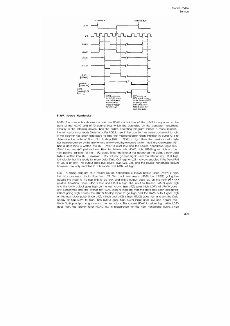
8/21/2019 HP5432 Microwave Frequency Counter
http://slidepdf.com/reader/full/hp5432-microwave-frequency-counter 243/364
Model 5342AService
8-369. Source Handshake
8-370. The source handshake controls the LDAV control line of the HP-IB in response to thestate of the HDAC and HRFD control lines which are controlled by the acceptor handshakecircuitry in the listening device. When the 5342A operating program finishes a measurement,
the microprocessor reads State In buffer U30 to see if the counter has been addressed to talk.If the counter has been addressed to talk, the microprocessor reads Interrupt In buffer U18 todetermine the state of Data Out flip-flop U9B. If U9B(9) is high, then the previous data bytehas been accepted by the listener and a new data byte maybe written into Data Out register U21.When a data byte is written into U21, U9B(9) is reset low and the source handshake logic setsLDAV low, two 2 periods later. When the listener sets HDAC high, U9B(9) goes high on thenext positive transition of the 2 clock. Since the listener has accepted the data, a new databyte is written into U21. However, LDAV will not go low again until the listener sets HRFD highto indicate that it is ready for more data. Data Out register U21 is always enabled if the Serial PollFF U29 is set low. The output data bus drivers, U22, U25, U31, and the source handshake circuitshowever, are only enabled in talk mode and LATN set high.
8-371. A timing diagram of a typical source handshake is shown below. Since U9B(9) is high,
the microprocessor clocks data into U21. This clock also resets U9B(9) low. U9B(9) going lowcauses the input to flip-flop U4B to go low, and U4B’S output goes low on the nextpositive transition. Since U4(9) is low and HRFD is high, the input to flip-flop U4A(2) goes highand the U4(5) output goes high on the next clock. When U4(5) goes high, LDAV at U36(3) goeslow. Sometimes later the listener set HDAC high to indicate that the data has been accepted.HDAC going high causes the U4(12) flip-flop input to go high and the U4(9) output goes highon the next clock pulse. Since U4(9) is high and U4(5) is high, U12(6) goes high and sets the DataReady fl ip-flop U9(9) to high. When U9B(9) goes high, U4(2) input goes low and causes theU4(5) flip-flop output to go low on the next clock. This causes LDAV to return high. After LDAVgoes high, the listener reset HDAC low in preparation for the next handshake cycle. Since
8-83

8/21/2019 HP5432 Microwave Frequency Counter
http://slidepdf.com/reader/full/hp5432-microwave-frequency-counter 244/364
Model 5342A
Service
U9B(9) is high, the microprocessor writes the second data byte into U21. U21(11) going highresets U9B(9) to a low which sets the U4B(9) flip-flop output low. However, the source hand-
shake logic can not indicate the presence of the second data byte (by pulling LDAV low) until
the listener sets HRFD high. When HRFD finally does go high, the output of flip-flop U4(5) goeshigh on the first clock after HRFD goes high. U4(5) going high sets LDAV low. When the listener
senses LDAV low, it sets HRFD low and the process continues as previously described.
8-372. ASSEMBLY LOCATIONS
8-373. Figures 8-19, 8-20, 8-21 and 8-22 shows the front (A1 Display Assembly) rear, top andbottom views, respectively, of the 5342A. The front and rear views show reference designators
of the front and rear panel controls, connectors, and indicators. The top view shows assemblylocations and adjustments.
8-374. TROUBLESHOOTING TO THE ASSEMBLY LEVEL(STANDARD INSTRUMENT)
8-375. Troubleshooting Technique
8-376. In the troubleshooting procedure outlined in Table 8-5, the 5342A is exercised through
a series of operating modes which are arranged in an increasing order of complexity. As can beseen in Table 8-6, an increasing number of assemblies is exercised as the operating modesprogress from, the first mode (power-up diagnostic) to the last mode (AUTO/1 GHz), By noting
the first mode in the sequence that fails, it is possible to isolate the defective assembly to aspecific group of assemblies by noting those assemblies common to the current (failed) test
and all previous tests (which passed). These common assemblies can be eliminated as beingthe source of the failure and only those assemblies which are not common to previous oper-
ating modes are examined. Table 8-7 is a list of the noncommon assemblies for each of the oper-ating modes and it is the basis for the troubleshooting procedure presented in Table 8-5.
8-84

8/21/2019 HP5432 Microwave Frequency Counter
http://slidepdf.com/reader/full/hp5432-microwave-frequency-counter 245/364
Model 5342A
Service
8-377. Tables 8-9 through 8-27 are individual troubleshooting procedures for various assem-
blies and assembly groups and are referenced in the overall troubleshooting of Ta ble 8-5.
By using the diagnostic modes of the 5342A, explained in Table 8-8, and the test equipment
listed in Tab le 1- 4, the troubleshooting procedure outlined in Tab le 8-5 and Tables 8-9 through
8-27 allows isolation of a failed assembly. By reading the detailed theory of operation of the
assembly and referencing the dc voltages and 5004A signatures provided on the individual
schematics, it should be possible to find the failed components.
8-378. Figure 8-23 is a detailed description block diagram of the 5342A and is valuable in
troubleshooting. Figure 8-9 shows the relationship of the assemblies listed in Table 8-6.
8-379. RECOMMENDED TEST EQUIPMENT
8-380. Test equipment recommended for troubleshooting, adjustments, operational verifica-
tion, and full performance testing is listed in Tab le 7-4. Equipment other than that listed may
be used if it meets the required characteristics.
Table 8-5. Overall Troubleshooting
1. POWER UP DIAGNOS TIC — Apply power to the 5342A and press front panel powerswitch to ON. The power-up diagnostic routine progressively lights all LED segments
in the 5342A display, from left to right. Finally, the following should be displayedbriefly:
If the 5342A powered up properly, go to step 2. If not:
a. If E’s fill the display, then RAM A14U12 failed the check sum routine exercised onpower up. A14U12 may be faulty if none of the address lines AØ-A15 or data linesDØ-D7 are stuck low or high. Check address lines and data lines on A14 for stucknodes (use current tracer such as 547A to find faulty device). Stuck data lines may
be caused by stuck ROM outputs (U1, U4, U7) or stuck buffer inputs (U2, U3). If1 is displayed, then ROM A14U7 failed the check sum routine exercised on power up.Since the RAM proved good (E’s were not displayed), the data lines and address linesbe OK. Replace A14U7.
1) If 2 is displayed, then ROM A14U4 failed the check sum routine exercisedon power up. Replace A14U4.
2) If 3 is displayed, then ROM A14U1 failed the checksum routine exercised on powerup. Replace A14U1.
3) If E16.0 is displayed (amplitude Option 002 only) then the check sum performed onPROM A16U3 failed. In this case, a new muItiplexer/PROM (matched pair) P/N05342-80005, must be ordered and installed (blue stripe exchange P/N 05342-80505)!
4) If E16.1 is displayed (amplitude Option 002 only) then the analog-to-digital con-version did not take place in A16U8 (U8 pin 36, BUSY, remains high).
b. Check for the clock on A14. If the clock is not present, check A24, A18, A17U8,
c. Go to Table 8-9 for A14 testing.
d. Go to Table 8-10 for power supply troubleshooting.
e. Go to Table 8-11 for A1, A2 testing.
8 -8 5
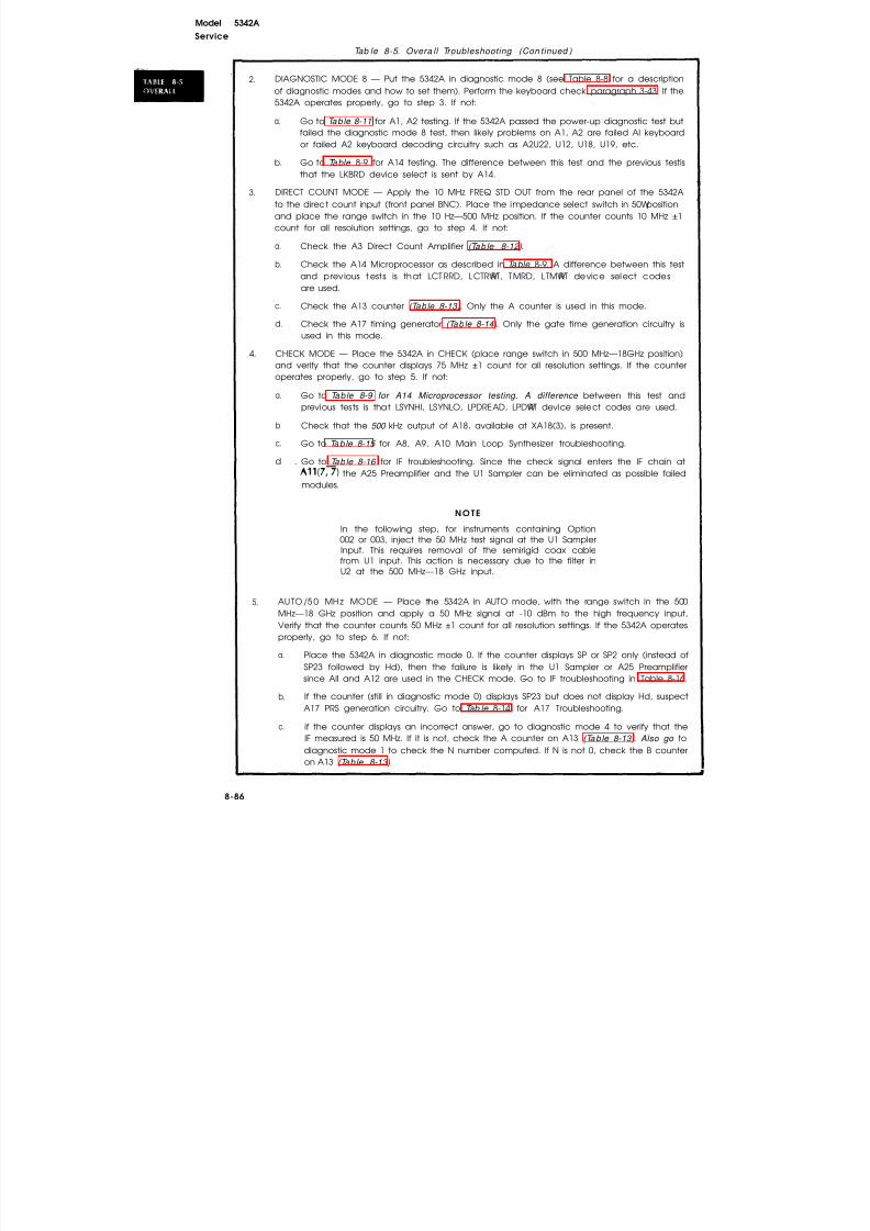
8/21/2019 HP5432 Microwave Frequency Counter
http://slidepdf.com/reader/full/hp5432-microwave-frequency-counter 246/364
TABLE 8-5
Model 5342A
Service
Tab le 8-5. Overa ll Troubleshooting (Con tinued )
2. DIAGNOSTIC MODE 8 — Put the 5342A in diagnostic mode 8 (see Table 8-8 for a descriptionof diagnostic modes and how to set them). Perform the keyboard check, paragraph 3-43. If the5342A operates properly, go to step 3. If not:
a. Go to Table 8-11 for A1, A2 testing. If the 5342A passed the power-up diagnostic test butfailed the diagnostic mode 8 test, then likely problems on A1, A2 are failed Al keyboardor failed A2 keyboard decoding circuitry such as A2U22, U12, U18, U19, etc.
b. Go to Table 8-9 for A14 testing. The difference between this test and the previous testisthat the LKBRD device select is sent by A14.
3. DIRECT COUNT MODE — Apply the 10 MHz FREQ STD OUT from the rear panel of the 5342Ato the direct count input (front panel BNC). Place the impedance select switch in 50Wpositionand place the range switch in the 10 Hz—500 MHz position. If the counter counts 10 MHz ±1count for all resolution settings, go to step 4. If not:
a. Check the A3 Direct Count Amplifier (Tab le 8-12).
b. Check the A14 Microprocessor as described in Table 8-9. A difference between this testand previous tests is that LCT RRD, LCTRWRT, TMRD, LTMWRT device select codesare used.
c. Check the A13 counter (Tab le 8-13). Only the A counter is used in this mode.
d. Check the A17 timing generator (Tab le 8-14). Only the gate time generation circuitry is
used in this mode.
4. CHECK MODE — Place the 5342A in CHECK (place range switch in 500 MHz—18GHz position)and verify that the counter displays 75 MHz ±1 count for all resolution settings. If the counteroperates properly, go to step 5. If not:
a. Go to Table 8-9 for A14 Microprocessor testing. A difference between this test andprevious tests is that LSYNHI, LSYNLO, LPDREAD, LPDWRT device select codes are used.
b. Check that the 500 kHz output of A18, available at XA18(3), is present.
c. Go to Table 8-15 for A8, A9, A10 Main Loop Synthesizer troubleshooting.
d . Go to Table 8-16 for IF troubleshooting. Since the check signal enters the IF chain atthe A25 Preamplifier and the U1 Sampler can be eliminated as possible failed
modules.
NOTE
In the following step, for instruments containing Option002 or 003, inject the 50 MHz test signal at the U1 SamplerInput. This requires removal of the semirigid coax cablefrom U1 input. This action is necessary due to the filter inU2 at the 500 MHz—18 GHz input.
5. AUTO /5 0 MH z MO DE — Place the 5342A in AUTO mode, with the range switch in the 500MHz—18 GHz position and apply a 50 MHz signal at -10 dBm to the high frequency input,Verify that the counter counts 50 MHz ±1 count for all resolution settings. If the 5342A operatesproperly, go to step 6. If not:
a. Place the 5342A in diagnostic mode 0. If the counter displays SP or SP2 only (instead of
SP23 followed by Hd), then the failure is likely in the U1 Sampler or A25 Preamplifiersince All and A12 are used in the CHECK mode. Go to IF troubleshooting in Table 8-16.
b. If the counter (still in diagnostic mode 0) displays SP23 but does not display Hd, suspectA17 PRS generation circuitry. Go to Tab le 8-14 for A17 Troubleshooting.
c. if the counter displays an incorrect answer, go to diagnostic mode 4 to verify that theIF measured is 50 MHz. If it is not, check the A counter on A13 (Tab le 8-13). Also go todiagnostic mode 1 to check the N number computed. If N is not 0, check the B counteron A13 (Tab le 8-13).
8-86
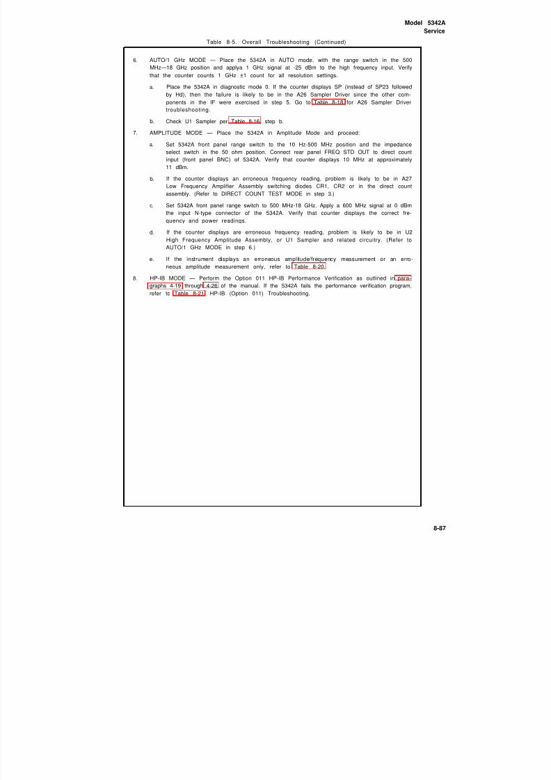
8/21/2019 HP5432 Microwave Frequency Counter
http://slidepdf.com/reader/full/hp5432-microwave-frequency-counter 247/364
Model 5342A
Service
Table 8-5. Overall Troubleshooting (Continued)
6. AUTO/1 GHz MODE — Place the 5342A in AUTO mode, with the range switch in the 500
MHz—18 GHz position and applya 1 GHz signal at -25 dBm to the high frequency input. Verify
that the counter counts 1 GHz ±1 count for all resolution settings.
a. Place the 5342A in diagnostic mode 0. If the counter displays SP (instead of SP23 followed
by Hd), then the failure is likely to be in the A26 Sampler Driver since the other com-
ponents in the IF were exercised in step 5. Go to Table 8-18 for A26 Sampler Driver
troubleshooting.
b. Check U1 Sampler per Table 8-16, step b.
7. AMPLITUDE MODE — Place the 5342A in Amplitude Mode and proceed:
a. Set 5342A front panel range switch to the 10 Hz-500 MHz position and the impedance
select switch in the 50 ohm position. Connect rear panel FREQ STD OUT to direct count
input (front panel BNC) of 5342A. Verify that counter displays 10 MHz at approximately
11 dBm.
b. If the counter displays an erroneous frequency reading, problem is likely to be in A27
Low Frequency Amplifier Assembly switching diodes CR1, CR2 or in the direct count
assembly. (Refer to DIRECT COUNT TEST MODE in step 3.)
c. Set 5342A front panel range switch to 500 MHz-18 GHz. Apply a 600 MHz signal at 0 dBm
the input N-type connector of the 5342A. Verify that counter displays the correct fre-
quency and power readings.
d. If the counter displays are erroneous frequency reading, problem is likely to be in U2
High Frequency Amplitude Assembly, or U1 Sampler and related circuitry. (Refer to
AUTO/1 GHz MODE in step 6.)
e. If the instrument displays an erroneous amplitude/frequency measurement or an erro-
neous amplitude measurement only, refer to Table 8-20.
8. HP-IB MODE — Perform the Option 011 HP-IB Performance Verification as outlined in para-
graphs 4-19 through 4-26 of the manual. If the 5342A fails the performance verification program,
refer to Table 8-21, HP-IB (Option 011) Troubleshooting.
8-87

8/21/2019 HP5432 Microwave Frequency Counter
http://slidepdf.com/reader/full/hp5432-microwave-frequency-counter 248/364
Model 5342A
Service
Table 8-6. Assemblies
Table 8-11
Table 8-11
Table 8-12
Table 8-17
Table 8-19
Table 8-17
Table 8-17
Table 8-15
Table 8-15
Table 8-15
Table 8-16
Table 8-16
Table 8-13
Table 8-9
Table 8-21
Table 8-20
Table 8-14
Table 8-5
Table 8-10
Table 8-10
Table 8-10
Table 8-10
Table 8-5
Table 8-16Table 8-18
Table 8-20
Tested by Test Mode
Table 8-20
NOTES: (1)
(2)
(3)
(4)
(5)
(6)(7)
(8)(9)
(10)
8-88

8/21/2019 HP5432 Microwave Frequency Counter
http://slidepdf.com/reader/full/hp5432-microwave-frequency-counter 249/364

8/21/2019 HP5432 Microwave Frequency Counter
http://slidepdf.com/reader/full/hp5432-microwave-frequency-counter 250/364
Model 5342A
Service
Table 8-8. Diagnostic Modes of the 5342A
1
“
To go to a diagnostic mode, press front panel set key twice (SET, SET) and then the number
corresponding to the desired mode. For example, pressing SET SET 8 goes into diagnostic
mode 8, the keyboard check. To leave a diagnostic mode, press RESET. The following de-
scribes the available diagnostic modes:
DIAGNOSTIC MODE FUNCTION
0 Displays mnemonics SP 23 followed by Hd. SP indicates that the
VCO’s are sweeping. 2 indicates that the unlatched power detector
is set, indicating an IF of sufficient amplitude and an IF in the range
of 50—100 MHz. 3 indicates that there is a proper IF for both the
Main VCO and OFFSET VCO. 3 is displayed after the VCO’s have
stopped sweeping. Hd indicates harmonic determination has been
complete. it is displayed at the end of the prs.
Counter displays Main OSC in MHz to 100 kHz, sign of IF (+ for
subtract and - for add) and the harmonic number N. For example:
IF is added
VCO = 344.2 MHz N = 10.99 (rounded to 11)
MHz kHz Hz
This is displayed at the end of the harmonic determination. (The
(-) sign of the IF indicates that the Nth harmonic of the VCO is less
than the unknown so that the IF must be added; the (+) sign of the
IF indicates that the Nth harmonic of the VCO is greater than the
unknown so that the IF must be subtracted.)
2 Counter continuously displays the contents of the A counter during
harmonic determination.
3 Counter continuously displays the contents of the B counter during
the harmonic determination.
4 Counter continuously displays the measured IF frequency. Reso-
lution determined by resolution selected before going to diagnostic
mode 4.
5 Put 5342A in AMPL mode (Option 002), then select diagnostic mode
(Option 002 only) 5. Counter display scontinously the corrected amplitude. Multiplexer
on front end is not switching between frequency and amplitude.
6 Put 5342A in AMPL mode (Option 002), then select diagnostic
(Option 002 only) mode 6. Counter display continuously uncorrected amplitude (not
corrected for level and frequency on A16). Multiplexer on front end
is not switching.
7 Sweeps Main VCO from 350 MHz to 300 MHz in 100 kHz steps.
Time between updates in VCO frequency determined by SAMPLE
RATE setting. To stay at a particular frequency, put SAMPLE RATE
to HOLD. (Remove input signal to counter, place counter in 500
MHz—18 GHz range and AUTO mode.)
8 Keyboard check. Refer to paragraph 3-43 for complete list of what
should be displayed when each key is pressed.
To return to normal operation, press RESET.
8-90

8/21/2019 HP5432 Microwave Frequency Counter
http://slidepdf.com/reader/full/hp5432-microwave-frequency-counter 251/364
TABLE 8-9
Model 5342A
Service
Table 8-9. A14 Microrprocessor Troubleshooting
1. Place the A14 Microprocessor Assembly on the extender board, P/N 05342-60036 which isshown below. Place the 5004A START and STOP probes on the B(4) test pin of the A14 ex-tender board. (Or, place on AP clip on U8 of A14 and place the START probe and the STOPprobe of a 5004A Signature Analyzer on A14U8(2), which is the most significant address lineout of the U21 microprocessor (A15).) Place the CLOCK probe of the 5004A on the VMA* 2
test point located in the upper righthand corner of A14. Place the GROUND probe of the5004A on the ground test point of A14.
2. Set the 5004A for positive slope on START, STOP, and CLOCK (all pushbuttons of the 5004Ashould be out). Apply power to the 5342A.
3. Place the 5342A in free-run mode by moving A14 switch S2A to the up position and all S1switches down (opens up data bus lines back into MPU U21). Ensure that the LX ROMswitch on the A14 extender board is in the up position. Press the RESET switch on the A14extender board.
8-91

8/21/2019 HP5432 Microwave Frequency Counter
http://slidepdf.com/reader/full/hp5432-microwave-frequency-counter 252/364
Model 5342AService
Table 8-9. A14 Microprocessor Troubleshooting (Continued)
4. Place the 5004A data probe on +5V and verify that the characteristic "1's" signature dis-played on the 5004A is 0003. If 0003 is not displayed, then the U21 microprocessor is notfree-running. If 0003 is displayed when the 5004A data probe is placed on +5V, go to step 5.
a. Check the clock inputs to the microprocessor by looking at the@II
(phase 1) clocktest point on A14 and the VMA@ test point. These signals should be as in thefollowing oscilloscope photos.
If these signals are not present, troubleshoot the clock generation circuitry U19,U22, U24, etc., on A14.
b. If these signals are present, check diodes CR2, CR3, and switches A14S1 and S2. Ifthese parts are good, then the U21 MPU is suspect.
c. With switches S1 and S2 set for freerun, check for correct inputs, as listed below:
8-92
*Time base of scope out of CAL in order to get onecomplete period in photo.

8/21/2019 HP5432 Microwave Frequency Counter
http://slidepdf.com/reader/full/hp5432-microwave-frequency-counter 253/364
Model 5342AService
Table 8-9. A14 Microprocessor Troubleshooting (Continued)
5. Place the 5004A data probe on the following address signal points (available on the A14 ex-tender board) and check that the proper free-run signatures are obtained:
If these signatures are obtained, go to step 6.
a. Check the signatures on the MPU side of buffer/drivers U16, U18, U8. Thesesignatures are adjacent to the A14 schematic. Correct or incorrect signaturesshould isolate the problem to either U21 or one or more of the buffer/drivers U16,U18, U8.
b. A signature may be incorrect because that particular address line is being heldlow or high by another assembly which is connected to the address bus. To checkthis possibility, isolate the A14 address bus from the other assemblies by setting
the address bus switches on the A14 extender board all open (low).
6. Place the 5004A data probe on the following device select codes and check that theproper free-run signatures are obtained:
DEVICE SELECT CODE LOCATION SIGNATURE
HDSPWRT U22(8) U05HLKBRD U20(7) FF48
LTIMRD U20(9) 7311LTIMWRT U20(10) 9FF7LCTRWRT U20(11) A732
LPDRD U20(12) A9FULPDWRT U20(13) 6A70LSYNHI U20(14) 1A9ULSYNLO
U20(15) 46A4LCTRRD U14(13) 94F1LHPIB U17(7) CC1A
LAMPMTR U17(6) 1P2A
If these signatures are correct, go to step 7.
a. If the signatures are not correct, check the inputs to the IC's with the incorrectsignatures. If the inputs are not correct, troubleshoot backwards along the signalflow, from output to input, until a device is found where the input exhibits acorrect signature but the output is incorrect. Change that IC.
b. If the inputs to U20, U22, U17 have good signatures, then either the IC is bad orthe output line is being held high or low by some other assembly connected tothat signal. To check this possibility, A14 must be isolated from the rest of theinstrument. Perform as follows:
(1) Remove A14 assembly and place it near lefthand side of instrument.
(2) Connect a clip lead from the +5V test pin on A17 to the +5V test pin on A14.
(3) Connect a clip lead from the gound test pin on A17 to the ground test pinon A14.
(4) Connect an AP clip to A14U22. Connect a clip lead from test pin TP1 on A17(1 MHz clock signal) to A14U22(4). The A14 assembly can now be exercised.
(5) Connect an AP clip to A14U8. Place the 5004A START and STOP inputs onA14U8(2).
8-93

8/21/2019 HP5432 Microwave Frequency Counter
http://slidepdf.com/reader/full/hp5432-microwave-frequency-counter 254/364
Model 5342AService
Table 8-9. A14 Microprocessor Troubleshooting (Continued)
(6) Connect the 5004A CLOCK to VMA.@J, test pin on A14 and GROUND toA14 ground test pin.
(7) Place the A14 board in free-run as in step 3.
(8) Measure the signatures again. If the A14 signatures are now good, thenthere is an assembly common to that signal which has a faulty input/output
buffer. To detect which assembly this is, put A14 back in the instrument andpull assemblies which are connected to the failed A14 signal output, oneat a time, until a good signature is obtained.
7. a. With the 5004A set up as in steps 1, 2, 3, place switch S2B in the down position:
b . Open the data bus switches on the A14 extender board as shown below:
c. Connect the 5004A data probe GND connector to chassis ground and the groundlead of the test pod to ground.
d. Connect the START of the 5004A to the R3 test point of the extender board andthe STOP to the R1 test point.
e. Set the 5004A for (-) slope START >
(+) slope on STOP f
(+) slope on CLOCK ~
f. Observe the following signatures: +5V - C690
Signal Name Location Signatures (for ROM Combinations listed)
A14U1 (P/N 1818-0329) A14U1 (1818-0698) A14U1 (1818-0698)A14U4 (1818-0330) A14U4 (1818-0697) A14U4 (1818-0697)A14U7 (1818-0331) A14U7 (1818-0331) A14U7 (1818-0706)
LDO A14A(3) AA7C 27H1 HP37LD1 A14A(4) 9UH5 H950 C256LD2 A14A(5) A4PF 0AP2 61P4LD3 A14A(6] F1P9 65PF 65PFLD4 A14A(7) P1P9 84U9 B4U9LD5 A14A(8) AOAC PC7U PC7ULD6 A14A(9) 312H COF3 4925
LD7 A14A(10) 54C7 5P8H 358C
g. If these signatures are good, go to step 8.
h. Check the inputs to A14U2, U3 by changing switch A14S2 as follows:
A14S2
8 - 9 4

8/21/2019 HP5432 Microwave Frequency Counter
http://slidepdf.com/reader/full/hp5432-microwave-frequency-counter 255/364
Model 5342A
Service
Tab/e 8-9. A14 Microprocessor Troubleshooting (Continued)
With the 5004A set up and connected as in steps 7d and 7e, take the followingsignatures:
Signal Name Location Signatures (for ROM Combinations listed)
A14U1 (P/N 1818-0329) A14U1 (1818-0698) A14U1 (1818-0698)A14U1 (P/N 1818-0330) A14U4 (1818-0697) A14U4 (1818-0697)
A14U7 (P/N 1818-0331) A14U7 (1818-0331) A14U7 (1818-0706)DO U3(9) 1FPC 9141 68A7D1 U3(12) 2945 6UF0 04F6D2 U3(4) 127F CF72 H774D3 U3(7) 7779 H37F H37FD4 U2(12) 5779 3269 3269D5 U2(9) 163C 5HPU 5HPUD6 U2(7) 87CH 0653 UUC5D7 U2(4) P227 P81H 831C
i. If these signatures are good, suspect buffers U2 and U3. If any of these signaturesare bad, then perform the following to isolate the problem to a particular ROM.
U7 ROM Test:
START and STOP of 5004A to R3 test point on A14 extender board
CLOCK of 5004A to VMAOOZ test point on A14START to (-) slope
>
STOP to (+) slopeJ
CLOCK to (+) slope<
GND of data probe to ground
A14S1 and A14S2 switches remain unchanged:
+5V — 826P
A14S1 A14S2
Signal Name Location Signatures (for ROM Combinations listed)
A14U1 (P/N 1818-0329) A14U1 (1818-0698) A14U1 (1818-0698)A14U1 (P/N 1818-0330) A14U4 (1818-0697) A14U4 (1818-0697)A14U7 (p/N 1818-0331) A14U7 (1818-0331) A14U7 (1818-0706)
DO U7(23) F3PC F3PC HP87D1 U7(22) CA11 CA11 CA12D2 U7(21) 52H7 52H7 52H4D3 U7(20) 3UP5 3UP5 3UP5D4 U7(19) U9H1 U9H1 U9H1D5 U7(18) 359F 359F 359F
D6 U7(17) OFUC OFUC 1197D7 U7(16) 3PCF 3PCF 3PCU
U4 ROM test — change the START and STOP of the 5004A to the R2 test point on theA14 extender board. All other settings remain unchanged.
+5V — 826P
8-95
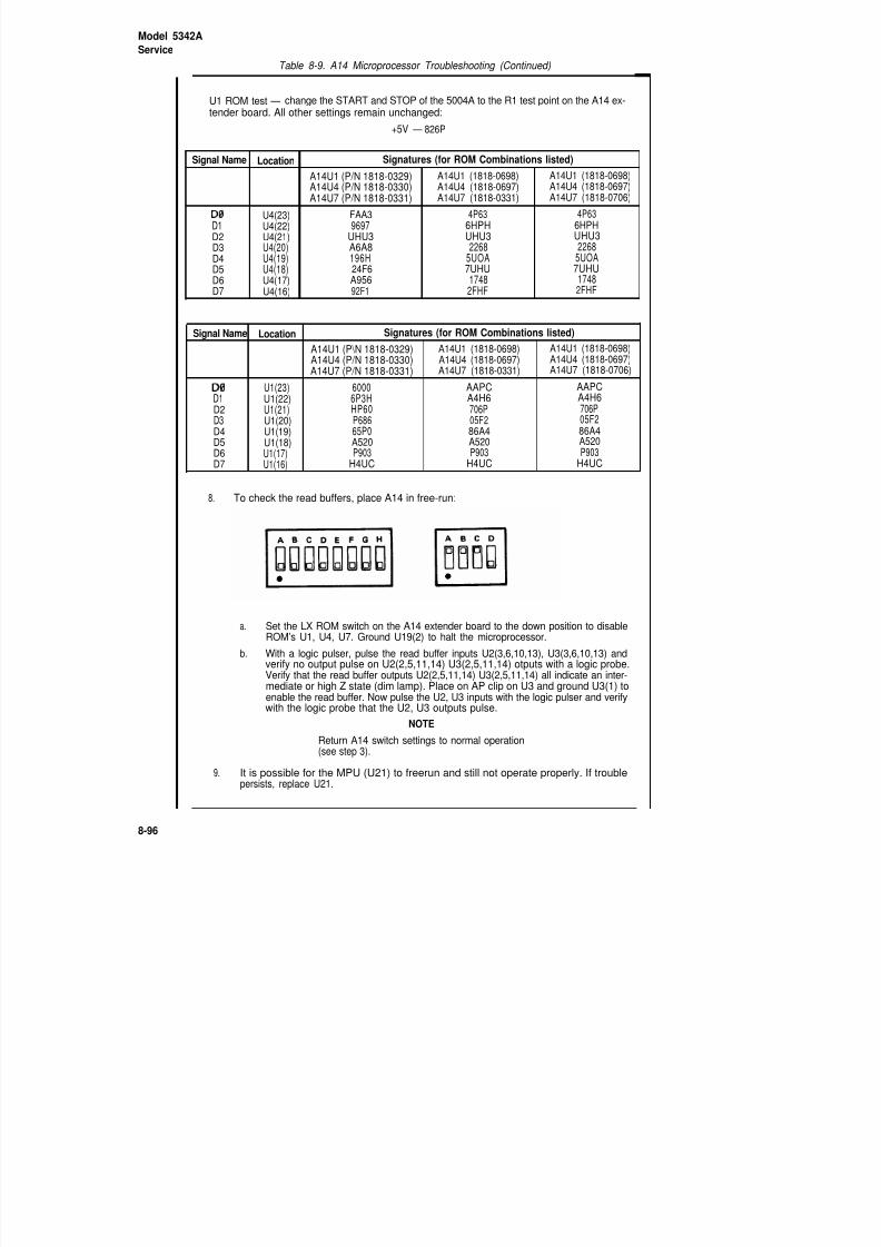
8/21/2019 HP5432 Microwave Frequency Counter
http://slidepdf.com/reader/full/hp5432-microwave-frequency-counter 256/364
Model 5342A
Service
Table 8-9. A14 Microprocessor Troubleshooting (Continued)
U1 ROM test — change the START and STOP of the 5004A to the R1 test point on the A14 ex-tender board. All other settings remain unchanged:
+5V — 826P
Signal Name Location Signatures (for ROM Combinations listed)
A14U1 (P/N 1818-0329) A14U1 (1818-0698) A14U1 (1818-0698)A14U4 (P/N 1818-0330) A14U4 (1818-0697) A14U4 (1818-0697)A14U7 (P/N 1818-0331) A14U7 (1818-0331) A14U7 (1818-0706)
DO U4(23) FAA3 4P63 4P63D1 U4(22) 9697 6HPH 6HPHD2 U4(21) UHU3 UHU3 UHU3D3 U4(20) A6A8 2268 2268D4 U4(19) 196H 5UOA 5UOAD5 U4(18) 24F6 7UHU 7UHUD6 U4(17) A956 1748 1748D7 U4(16) 92F1 2FHF 2FHF
Signal Name Location Signatures (for ROM Combinations listed)A14U1 (P\N 1818-0329) A14U1 (1818-0698) A14U1 (1818-0698)A14U4 (P/N 1818-0330) A14U4 (1818-0697) A14U4 (1818-0697)A14U7 (P/N 1818-0331) A14U7 (1818-0331) A14U7 (1818-0706)
DO U1(23) 6000 AAPC AAPCD1 U1(22) 6P3H A4H6 A4H6D2 U1(21) HP60 706P 706PD3 U1(20) P686 05F2 05F2D4 U1(19) 65P0 86A4 86A4D5 U1(18) A520 A520 A520D6 U1(17) P903 P903 P903D7 U1(16) H4UC H4UC H4UC
8. To check the read buffers, place A14 in free-run:
a. Set the LX ROM switch on the A14 extender board to the down position to disableROM’s U1, U4, U7. Ground U19(2) to halt the microprocessor.
b. With a logic pulser, pulse the read buffer inputs U2(3,6,10,13), U3(3,6,10,13) andverify no output pulse on U2(2,5,11,14) U3(2,5,11,14) otputs with a logic probe.
Verify that the read buffer outputs U2(2,5,11,14) U3(2,5,11,14) all indicate an inter-mediate or high Z state (dim lamp). Place on AP clip on U3 and ground U3(1) toenable the read buffer. Now pulse the U2, U3 inputs with the logic pulser and verifywith the logic probe that the U2, U3 outputs pulse.
NOTE
Return A14 switch settings to normal operation(see step 3).
9. It is possible for the MPU (U21) to freerun and still not operate properly. If troublepersists, replace U21.
8-96

8/21/2019 HP5432 Microwave Frequency Counter
http://slidepdf.com/reader/full/hp5432-microwave-frequency-counter 257/364
TABLE 8-10
Model 5342A
Service
Table 8-10, A19, A20, A21 Power Supply Troubleshooting
It is extremely dangerous to troubleshoot the A19 assembly ofthe power supply if an isolation transformer is not used. A19 isconnected directly to the power main. Use an isolation trans-former such as Allied Electronics P/N 705-0048 (for 120V ac) to
isolate the instrument from the power main. The measurementsin this troubleshooting procedure may be made only if an iso-lation transformer is used.
1. Connect 5342A power cord to isolation transformer.
2. The first step in power supply troubleshooting is to check the state of the green LED onA20 and the red LED on A21. If the green LED is on and the red LED is off, then the+5V(D) supply is working properly. If the red LED is on and the green LED is off, thenone or more of the voltage outputs of A20, A21 may be drawing excessive current. Evenif the green LED is on, one of the regulated outputs of A21 may be shut down due toexcessive current. Check the following voltage levels:
SUPPLY LOCATION VALUE
*lf this voltage is not correct, adjust A21R17 before making other voltage measurements.
NOTE
If one or more of the voltage outputs is at ground, then a probablecause is that one of the assemblies in the instrument connected
to that voltage output has a short to ground. Remove assembliesconnected to that voltage output, one at a time, until the shortis removed. After removing an assembly, replace it in the instru-ment if that assembly is not the problem. This must be done be-cause the power supply looses regulation if not run at approxi-mately 75% of full load. The following table shows which as-semblies are connected to the various supply voltages:
SUPPLY FROM TO
The waveforms in the following paragraph require using anisolation transformer as described in the CAUTION precedingstep 1.
8-97

8/21/2019 HP5432 Microwave Frequency Counter
http://slidepdf.com/reader/full/hp5432-microwave-frequency-counter 258/364
TABLE 8-10
Model 5342AService
Table 8-10. A19, A20, A21 Power Supply Troubleshooting (Continued)
3. A21 Troubleshooting
a. Pull A19 and A20 from the instrument and put A21 on an extender board. Plugthe 5342A to the line but leave the ON/STBY switch in STBY. Measure the voltageat test lead TLS (labeled TLS 13.5V), which is the positive side of A21C20, andverify that this voltage is approximately 13.5 volts. If not, suspect rectifier A21CR2
or oven transformer T4.
b. With the 5342A still in STBY, monitor test points TP2 and TP3 on A21 with anoscilloscope. Short TPJ and TPG (lower right corner TP on A21) together. Observethe following waveforms:
Now remove the short from TPJ to TPG and observe:
c. Connect a clip lead to A21TP4 and momentarily ground the other end to the chassis.Observe red LED turn on for approximately 1-2 seconds and waveforms at TP2,TP3 go to a constant +13 volts for same duration. If not, suspect A21U3.
8-98

8/21/2019 HP5432 Microwave Frequency Counter
http://slidepdf.com/reader/full/hp5432-microwave-frequency-counter 259/364
Model 5342AService
Table 8-10. A19, A20, A27 Power Supply Troubleshooting (Continued)
4. With A21 still on extender board (remove short from TPJ to TPG), insert A19 on anextender board into the instrument (A20 is still out of the instrument). Leave the 5342Aline switch in STBY. The waveform at A19TP4 indicates that A19 transformers T1 andT2 are operating properly.
Now switch front panel line switch to ON and observe:
If the above waveform is not present, check the collector of A19Q1 for 300V (with re-spect to the test point TPG). If 300V dc is not present, suspect input rectifier A19CR1and associated circuitry. If 300V dc is present, suspect open transistors Q1 and Q2.
8-99

8/21/2019 HP5432 Microwave Frequency Counter
http://slidepdf.com/reader/full/hp5432-microwave-frequency-counter 260/364
Model 5342AService
Table 8-10. A19, A20, A21 Power Supply Troubleshooting (Continued)
5. Fabricate the following special test extender board shown below. This board is usefulbecause, by placing a 1 Kfl load in series with the A20T1 transformer, the current drawnfrom transistors A19Q1) Q2 is limited. If A19Q1, Q2 have failed because of excessivecurrent (due to a failure in the A21 overcurrent protection circuitry), then replacingA19Q1, Q2 and using the 1 Kfl load allows the power supply to be checked out withoutdanger of blowing A19Q1, Q2 again.
a. Take a 22-pin extender board (such as HP P/N 05342-60034) and cut the traces onpin 8 and
~
as shown below.
b, Solder a 1 Kfl, 20W resistor (HP P/N 0819-0006) above and below the cut as shown:
c. Insert A20 in the above extender board into the instrument. Insert A21 (on stand-ard HP P/N 05342-60034 extender board) into the instrument. Short A21TPJ toTPG (low right test point). Insert A19 on extender into instrument. MonitorA19TP4 with the scope probe ground on A19 TPG test point (emitter of Q2). If anisolation transformer is not used, do NOT make this measurement.
8-100

8/21/2019 HP5432 Microwave Frequency Counter
http://slidepdf.com/reader/full/hp5432-microwave-frequency-counter 261/364
Model 5342AService
Table 8-10, A19, A20, A21 Power Supply Troubleshooting (Continued)
d. Remove special extender board and remove the short between A21TPJ and TPG.Insert A20 into XA20.
Green LED on A20 should be lit.
e. Now monitor A19TP5 and observe (adjust A19R1 for -1V on trailing edge):
8-101

8/21/2019 HP5432 Microwave Frequency Counter
http://slidepdf.com/reader/full/hp5432-microwave-frequency-counter 262/364
TABLE 8-11
Model 5342AService
Table 8-11. A1. A2 Keyboard/Display Troubleshooting
8-102
1. First verify that HDSPWRT at XA14B(10) pulses high when power is applied to the5342A by using a logic probe such as the 545A. If not, troubleshoot A14 to obtain anHDSPWRT signal.
2. If HDSPWRT is present on the power up and pulses consistently thereafter but the dis-play/keyboard still does not operate properly, remove the A1, A2 and front panelassembly as follows:
a. Remove front panel, sample rate knob with allen wrench.
b. Remove BNC connector nut and type N connector nut.
c. Pull off the two coax cables connected to A1J3 and A1J1.
d. Remove the two chassis screws from each side strut holding the front panel tothe strut.
e. Pull off front panel assembly carefully.
f. Remove 5 screws holding A1, A2 to front panel.
g. Pull out A1, A2 which are sandwiched together by a center press-on connector.
h. Make sure ribbon cable remains connected to A2.
3. Remove A14 from the 5342A chassis. With a clip lead, ground the following pins andobserve the display for the following lighted LED segments:
a. A2U1(3) all (b) segments and dBm light should lightA2U1(6) all decimal points and blue key should lightA2U1(8) all (d) segments, REM light, and MAN key should lightA2U1(11) all (c) segments, GATE light, and OFS MHz key should light
b. A2U4(3) all (g) segments and RECALL key should lightA2U4(6) all (a) segments and FM light and AMPL key should lightA2U4(8) all (e) segments and AUTO key should lightA2U4(11) all (f) segments, SET key and OFS dB key should light
c. If all segments light as specified, then the LED’s A1DS11 through DS21 and theassociated transistor drivers on A1 are operating properly. In addition, the scanclock comprised of A2U5, U3, U13, U6, and the column scanners A2U2, U7 areoperating properly.
d. If only one segment in the display lights, troubleshoot the scan clock and columnscanners on A2.

8/21/2019 HP5432 Microwave Frequency Counter
http://slidepdf.com/reader/full/hp5432-microwave-frequency-counter 263/364
TABLE 8-11
Model 5342A
Service
Table 8-11. A1, A2 Keyboard/Display Troubleshooting (Continued)
4. If the 5342A does not perform the power up diagnostic but A1, A2 properly perform thetest described in step 3, the probable cause of the failure is A2U11, U8 (TTL RAM memory),A2U16 (data bus buffer), A2U5, U13 (write enable generation), or U17 (multiplexer).
5. If the 5342A performs the power-up diagnostic but does not perform the diagnosticmode 8 keyboard check, the probable cause of the problem is the key decoding circuitry
on A2 consisting of U13A, USC, U18, U19, and U12. To test this circuitry, perform thefollowing tests with A14 still removed from instrument:
a. Monitor U10(8) with a logic probe and verify that each time a key is depressed,U10(8) goes low. To cause U10(8) to return to high, ground U22(1) momentarily.This verifies that pushing a key generates an interrupt request (LIRQ) and thatreading the keyboard (LKBRD) clears the interrupt request.
b. Place AP clip on U22 and monitor the outputs of latch U22 by grounding U22(1)and verify that when a key is pressed, the latch stores the following data:
KEY U22(3) (4) (5) (6)
0 0 0 0 01 1 0 0 02 0 1 0 0
3 1 1 0 04 0 0 1 05 1 0 1 06 0 1 1 07 1 1 1 08 0 0 0 19 1 0 0 1l o 1 0 1
ENTER 1 1 0 1
c. Monitor U12(2) and verify that when any of the leftmost grouping of keys (AUTO,MAN, RESET, etc.) is pressed, U12(2) is high and that when any of the rightmostgrouping of keys (0, 1, 2, etc.) is pressed, U12(2) is low. This verifies that the top/ bottom row decoder U19A is operating properly.
d. If the A2 assembly passes all the above, then the most probable cause of the problemis the A2U12 bus driver. Another possible cause is that the A14U2 MPU does notrespond to the LIRQ signal.
8-103

8/21/2019 HP5432 Microwave Frequency Counter
http://slidepdf.com/reader/full/hp5432-microwave-frequency-counter 264/364
TABLE 8-12
Model 5342A
Service
Table 8-12. A3 Direct Count Amplifier Troubleshooting
To check that the direct count amplifier is working, connect the 10 MHz FREQ STD rearpanel output to thedirect count input (front panel BNC). Place the range switch in the 10 Hz—500 MHz range and the impedance select to 500. Monitor TP1 of A3 for the following wave-form (TP1 is the output of Schmitt Trigger U5).
NOTE
Check that the output of A3, DIRECT B available at XA3(1), isdivided by four and that DIRECT A available at XA3(2) is dividedby two.
8-104

8/21/2019 HP5432 Microwave Frequency Counter
http://slidepdf.com/reader/full/hp5432-microwave-frequency-counter 265/364
TABLE 8-13
Model 5342AService
Table 8-13. A13 Counter Troubleshooting
1. Apply approximately 50 MHz signal at -10 dBm to the high frequency input of the5342A. Put the counter in diagnostic mode 2 (press SET, SET, 2) to read the contentsof the A counter. The A counter should read approximately 8,200,000. Put the 5342Ain diagnostic mode 3 to read the B counter. it should be the same reading as A, ±1 count(provided the stability of the 50 MHz source is that good). If this is true, then A13 isgood. If it is not true, A13 may be at fault (as well as A17 for the prs generation andgate time generation).
2. Check the inputs to the A counter as follows: Apply 10 MHz FREQ STD OUT on rearpanel to the direct count input (fron panel BNC) with 50J_I position selected. Check thefollowing A counter test points (since 10 MHz is divided by four on A3, TP6 which dividesA3 output by 2, should have a period of 8x1OO ns = 800 ns and TP7, which divides A3output by four should have a period of 16x100 ns = 1.6 PS):
3. Check the inputs to the B counter as follows: Apply a 50 MHz, -10 dBm signal to thehigh frequency input and select the 500 MHz—18 GHz range. Put the 5342A in AUTO andpush RESET to cause the counter to go to the prs generation, thus enabling the Bcounter. Place the rear panel FM switch to the FM position so that the B counter is
enabled for 2.1 seconds.
8-105

8/21/2019 HP5432 Microwave Frequency Counter
http://slidepdf.com/reader/full/hp5432-microwave-frequency-counter 266/364
TABLE 8-13
Model 5342AService
Table 8-13. A13 Counter Troubleshooting (Continued)
4. Test the outputs of U1 and U2 for activity by applying a 50 MHz, -10 dBm signal to thehigh frequency input. Place the counter in AUTO, 500 MHz—18GHz range, and diagnosticmode 2 so that the prs is continually generated, Monitor TP2 and TP3 with an oscillo-scope. If the signals appears much different than the waveform shown below, one ormore of the U3 buffers have probably failed. Use a logic pulser and logic probe to checkout the U3, U7 buffers. An HP 1607A Logic State Analyzer may be used to check out theactual data going back to the microprocessor as shown in step 5.
When the counter is not in diagnostic mode 2 but is just measuring the 50 MHz signal,the waveform below shows activity at the A counter (counting the IF) but none at the
B counter.
5. 1607A check out of A13
a. Put A13 on extender board and put AP clips on A13U3, U5, U8, and U10. Connectthe following 1607 data bit lines as follows:
1607 Data Inputs A13 Connections Description
b. Set 1607A to repetitive, Table A, word trigger, delay off and start display. Put bits15-7 in the OFF (don’t care) position. Place the 5342A in CHECK mode and 1 MHzresolution. Select each of the following trigger words (EXAMPLES 1, 2, and 3) andverify the proper 1607A display in the don’t card bits of the trigger word.
8-106

8/21/2019 HP5432 Microwave Frequency Counter
http://slidepdf.com/reader/full/hp5432-microwave-frequency-counter 267/364
Model 5342A
Service
Example 1: CHECK Mode - 1 MHz Resolution
OFF DATA BITS TRIGGER WORDCOMMENTS SHOULD BE: (DATA BITS)
10 9 8 7 6 5 4 3 2 1 0
*These two bits ignored in 1 1 * * 0 1 0 0 0 0 0CHECK since they repre-sent state of dividers on A3.
This reads out least signifi-cant counts. In this casewe’re reading state ofdivider U12B (bit 9) anddivider U16B (bit 10). Countequals 3 in this case.
Bit 7 = U17(5) output 1 0 0 0 0 1 0 1 0 0 0Bit 8 = U17(9) outputBit 9 = U17(2)Bit 10= U17(12)
Count = 8 in this case.
Bit 7 = U13(5) output 0 0 0 1 0 1 1 0 0 0 0Bit 8 = U13(9) output
Bit 9 = U13(2) outputBit 10= U13(12)Count = 1 in this case.
Bit 7 = U1(15) 100decade 0 0 0 0 0 1 1 1 0 0 0
Bit 8 = U1(16) 100decade
Bit 9 = U1(1) 100decade
Bit 10 = U1(2) 100decade
Count = 0
Bit 7 = U1(15) 101decade 0 0 0 0 0 1 1 1 0 0 1
Bit 8 = U1(16) 101decade
Bit 9 = U1(1) 101decade
Bit 10= U1(2)Count = 0
Bit 7 = U1(15) 102
decade 0 0 0 0 0 1 1 1 0 1 0Bit 8 = U1(16) 10
2decade
Bit 9 = U1(1) 102decade
Bit 10 = U1(2) 102decade
Count = 0
Bit 7 = U1(15) 103decade 0 0 0 0 0 1 1 1 0 1 1
Bit 8 = U1(16) 103decade
Bit 9 = U1(1) 103decade
Bit 10 = U1(2) 103decade
Count = 0
Bit 7 = U1(15) 104decade 0 0 0 0 0 1 1 1 1 0 0
Bit 8 = U1(16) 104decade
Bit 9 = U1(1) 104decade
Bit 10 = U1(2) 104
decadeCount = 0
Bit 7 = U1(15) 105decade 0 0 0 0 0 1 1 1 1 0 1
Bit 8 = U1(16) 105decade
Bit 9 = U1(1) 105decade
Bit 10 = U1(2) 105decade
Count = 0
Total Count = 3+4(8+10) = 75 counts Multiply all the counts after the 1st by 4 since(Count display 75 MHz) the input to the decade counters has essentially been
prescaled by 4.
8-107
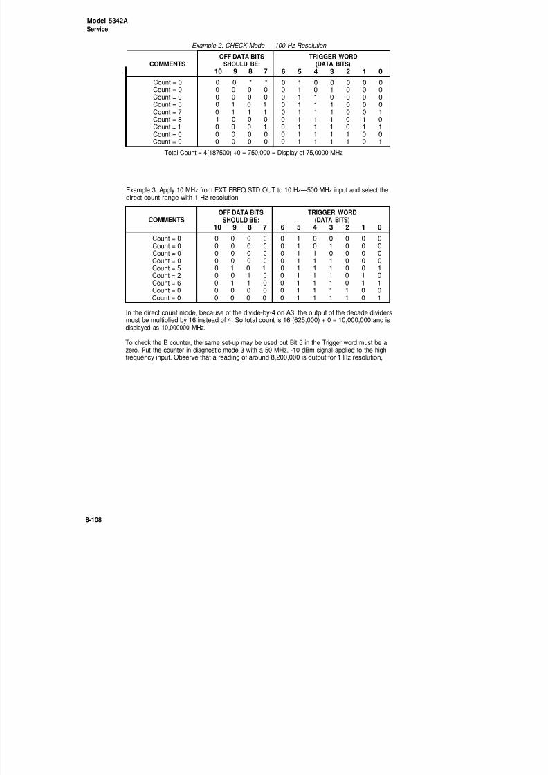
8/21/2019 HP5432 Microwave Frequency Counter
http://slidepdf.com/reader/full/hp5432-microwave-frequency-counter 268/364
Model 5342A
Service
Example 2: CHECK Mode — 100 Hz Resolution
COMMENTS
Count = 0Count = 0Count = 0
Count = 5Count = 7Count = 8Count = 1Count = 0Count = 0
OFF DATA BITSSHOULD BE:
10 9 8 7
0 0 * *0 0 0 00 0 0 0
0 1 0 10 1 1 11 0 0 00 0 0 10 0 0 00 0 0 0
TRIGGER WORD(DATA BITS)
6 5 4 3 2 1 0
0 1 0 0 0 0 00 1 0 1 0 0 00 1 1 0 0 0 0
0 1 1 1 0 0 00 1 1 1 0 0 10 1 1 1 0 1 00 1 1 1 0 1 10 1 1 1 1 0 00 1 1 1 1 0 1
Total Count = 4(187500) +0 = 750,000 = Display of 75,0000 MHz
Example 3: Apply 10 MHz from EXT FREQ STD OUT to 10 Hz—500 MHz input and select thedirect count range with 1 Hz resolution
COMMENTS
Count = 0Count = 0Count = 0Count = 0Count = 5Count = 2Count = 6Count = 0Count = 0
OFF DATA BITSSHOULD BE:
10 9 8 7
0 0 0 00 0 0 00 0 0 00 0 0 00 1 0 10 0 1 00 1 1 00 0 0 00 0 0 0
TRIGGER WORD(DATA BITS)
6 5 4 3 2 1 0
0 1 0 0 0 0 00 1 0 1 0 0 00 1 1 0 0 0 00 1 1 1 0 0 00 1 1 1 0 0 10 1 1 1 0 1 00 1 1 1 0 1 10 1 1 1 1 0 00 1 1 1 1 0 1
In the direct count mode, because of the divide-by-4 on A3, the output of the decade dividersmust be multiplied by 16 instead of 4. So total count is 16 (625,000) + 0 = 10,000,000 and isdisplayed as 10,000000 MHz.
To check the B counter, the same set-up may be used but Bit 5 in the Trigger word must be azero. Put the counter in diagnostic mode 3 with a 50 MHz, -10 dBm signal applied to the highfrequency input. Observe that a reading of around 8,200,000 is output for 1 Hz resolution,
8-108

8/21/2019 HP5432 Microwave Frequency Counter
http://slidepdf.com/reader/full/hp5432-microwave-frequency-counter 269/364
Model 5342AService
Table 8-14. A17 Timing Generator Troubleshooting
1. The A17 Timing Generator has a number of outputs:
a. LO SWITCH at XA17(1) which switches the AS multiplexer and A13 counters in apseudorandom sequence after acquisition.
b. LDIR GATE at XA17(~) which gates the main gate on A3 for direct countmeasurements.
c. LIF GATE at XA17(;) which gates counter A on A13 for measuring the IF.
d. CLOCK at XA17(4) which drives A14.
e. When A17 is read by the microprocessor, the D4 line is examined to see if the gatetime is over. The D1 line indicates the end of the prs. The D2 line indicates theend of the sample rate run down.
2. LO SWITCH verification. To verify that the LO SWITCH signal is operating properly, the5342A must be able to acquire so that the counter can be forced into its harmonic deter-mination routine. This means that A25, U1, A11, A12 must be working properly. To checkLO SWITCH, apply a 50 MHz signal, -10 dBm, to the high frequency connector and put the5342A in the 500 MHz—18 GHz range. The LO SWITCH signal at XA5~ should appear:
The time during which the signal switches between high and low levels in a pseudo-random fashion should be 360 ms. The time where the signal is high and not switching iscontrolled by the front panel sample rate control and resolution of counter. If the rearpanel switch is placed in the FM position, then the time during which the signal is switch-ing should extend to 2.1 seconds (actually 2.096).
A sample of what the sequence looks like is shown below where the sweep speed of thescope has been increased to 100 ps :
If LO SWITCH is stuck low, then the 5342A will not acquire even if all the IF circuitryis working properly. This is due to the fact that during acquisition, a 1 ps measurementis made on the IF and this requires that LO SWITCH go high to select the A counter onA13. This measurement is made to insure that the IF is in the proper frequency range.The above troubleshooting procedure will not work in this case since diagnostic mode 3can not be entered. This condition would be evidenced by the counter displaying SP2in diagnostic mode 0.
8-109

8/21/2019 HP5432 Microwave Frequency Counter
http://slidepdf.com/reader/full/hp5432-microwave-frequency-counter 270/364
TABLE 8-14
Model 5342AService
Table 8-14. A17 Timing Generator Troubleshooting (Continued)
IF LO SWITCH is not present, check the TP5 test point on A17 to see if the prs gener-ator is working. Put the counter in diagnostic mode 2 for continual prs generation.TP5 is high during the prs and should remain high for 360 ms (normal or CW modeon rear panel) or for 2.096 seconds (FM mode).
3. Troubleshooting the A17 prs generator.
To troubleshoot the prs generator on A17 (consisting of A17U7, U4, U5, U2, U1, andvarious gates), pull the A18 time base buffer board from the instrument to disable the
1 MHz clock into A17. Put A17 on an extender board, connect logic probe and logicpulser power leads to A17 +5V and ground, and perform as follows:
a. U7, U4, U5 SHIFT REGISTER CHECK
1) Put AP clip on U3 and connect clip lead from U3(9) to ground. Verify thatU5(1) is high. Clear U7, U4, U5 by applying 1 pulse with logic pulser toTP5 test point. Monitor U5(9) with logic probe to see that the clear inputpulses low (if clear input powers up low, then apply a pulse to U19(9) thento U14(2) to cause the clear input to go high).
2) Apply logic pulser to TP4 test point and monitor the shift register outputs.
After 1 pulse at TP4, U5(3) should go from low to high.
Apply 2 more pulses at TP4, U5(5) should go from low to high.
Apply 12 more pulses at TP4, U4(12) should go from low to high.
Apply 5 more pulses at TP4, U7(6) should go from low to high.b. U2, U1 Counters Check
1) Connect AP clip to U3. Connect clip lead from U3(1) to ground.
2) Verify that U1(1) is high. If not, pulse U19(9), then U14(2) with logic pulser.Verify that U2(3) is high and U2(5) is low. If not, pulse U19(9).
3) Connect another clip lead from U3(5) to ground. Verify that U1(9) is low.Move clip lead from U3(5) to U3(6) so that U3(6) is grounded. Verify thatU1(9) is high. This loads data into U1 and U2 counters.
4) Monitor U1(15) with logic probe and pulse TP4 test point with pulser 14times. ON 14th clock, U1(15) should pulse high.
8-110

8/21/2019 HP5432 Microwave Frequency Counter
http://slidepdf.com/reader/full/hp5432-microwave-frequency-counter 271/364
Model 5342AService
Table 8-14. A17 Timing Generator Troubleshooting (Continued)
4. A17 LDIR GATE and LIF GATE troubleshooting.
a. Set the 5342A to 10 Hz—500 MHz range, sample rate full CCW , no input signal, and100 Hz resolution. With an oscilloscope, monitor LDIR GATE at XA3(5) and TP6 onA17 as shown below:
b. As the resolution is changed, the width of the gate signal (TP6 high) should vary as
follows: Resolution Width
1 MHz 1/.ls
100 kHz 10ps
10 kHz 100 ps
1 kHz 1 ms100 Hz 10 ms10 Hz 100 ms1 Hz 1 sec
c. Change the range of the 5342A to the 500 MHz—18 GHz range and place thecounter in MAN mode and observe:
d. As the resolution is change, the width of the gate signal should vary as follows:
Resolution Width
1 MHz 10 /ls
100 kHz Four 10PS
width pulses, 100ys
between each10 kHz Four 100
MS
width pulses, 100AS
between each1 kHz Four 1 ms width pulses, 100
ps
between each100 Hz Four 10 ms width pulses, 100
ps
between each10 Hz Four 100 ms width pulses, 100 ps between each1 Hz 1 sec
For resolutions from 100 kHz to 10 Hz, each gate time consists of four gate signalsseparated by 100
ps
dead time.
8-111

8/21/2019 HP5432 Microwave Frequency Counter
http://slidepdf.com/reader/full/hp5432-microwave-frequency-counter 272/364
Model 5342A
Service
Table 8-14. A17 Timing Generator Troubleshooting (Continued)
5. IF LDIR GATE or LIF GATE signals are not present, place A17 on an extender board andmonitor A17U16(1), the output of the A16 time base generator. Place the 5342A in 10 Hz—500 MHz range, sample rate full CCW, and 1 kHz resolution and observe:
Only the first period of the U16(11) output is used to generate the LDIR GATE is used togenerate the LDIR GATE signal as shown below:
8-112

8/21/2019 HP5432 Microwave Frequency Counter
http://slidepdf.com/reader/full/hp5432-microwave-frequency-counter 273/364
TABLE 8-15
Model 5342AService
Table 8-15. A8, A9, A10 Main Loop Synthesizer Troubleshooting
1. To test if the A9 Main Loop Amplifier and A10 Divide-by-N are operating properly,put the 5342A in AUTO and select the 500 MHz—18 GHz range. Disconnect any inputsignal. In diagnostic mode zero (press SET, SET, 0), the counter should display SP,indicating that it is sweeping the synthesizers. The MAIN CNTRL signal, measured atXA8(1), should look like:
The sweep up time is approximately 90 ms while the sweep down time is 60 ms. If thissignal is present, then A9, A10, and part of A8 as well as the ROM program on A14, areoperating properly.
2. To test if the A8 Main VCO is operating properly, put the 5342A in MANUAL mode,500 MHz—18 GHz range and set the MANUAL center frequency to the values in thefollowing table. Connect a coax cable, with BNC connector on one end and alligatorclips on the other, from XA5(10) to the 5342A direct count input (front panel BNC). XA5(10)is the Main OSC signal and will be measured by the 5342A if the range switch ischanged to the 10 Hz—500 MHz range (impedance select should be in 500). To changeMANUAL center frequency, place the range switch back in the 500 MHz—18 GHzposition and SET MAN. Verify that the counter measures the proper MAIN OSC fre-quency for each of the MANUAL center frequencies selected.
MAN CENTER MAIN OSCFREQ FREQ
500 MHz 300.0 MHz550 MHz 312.5 MHz
600 MHz 337.5 MHz650 MHz 350.0 MHz
Also test the output level of the A8 outputs. Using an RF Millivoltmeter with a high Zprobe, the following A8 output levels should be measured (±100 mV):
XA8(7) MAIN OSC 500 mV rmsXA8Q)
MAIN VCO 250 mV rmsXA8(5) DIV N 250 mV rms
These levels are essentially independent of frequency.
If steps 1 and 2 pass the test, then the Main Loop Synthesizer is working properly. Ifnot, proceed to step 3.
3. A8 FREE RUN FREQUENCY CHECK. ConnectXA5(~O),
the MAIN OSC signal, to thedirect count input (front panel BNC), of the 5342A. Use a coax cable, BNC on one endand alligator clips on the other. With a jumper, short MAIN CNTRL, A9TP1, to ground.
The 5342A should read approximately 325 MHz f2 MHz). If not, adjust A8R22. If nosignal is present, repair A8. (Test all of the A8 outputs for a signal.)
8-113

8/21/2019 HP5432 Microwave Frequency Counter
http://slidepdf.com/reader/full/hp5432-microwave-frequency-counter 274/364
Model 5342AService
Table 8-15. A8, A9, A10 Main Loop Synthesizer Troubleshooting (Continued)
4. Troubleshooting A9 and A10.
Put A10 on an extender board and put an AP clip on A10U2. Connect scopes probes toU2(5) which is MAIN AO1 and U2(10) which is MAIN A@2. Ground TP1 on A9 with aclip lead. This causes the A8 VCO to go to its free run frequency of 325 MHz. Put the5342A in AUTO, 500 MHz—18 GHz range, and no input. This causes the 5342A to sweepthe synthesizers. Verify that the U2 phase detector outputs appear as follows:
If these signals are not present, then either the divide-by-N or the phase detector onA10 is faulty. If this signal is present but there is no MAIN CNTRL sweep signal at XA8(7
as in step 1, then A9 is faulty.
5. The following test determines if the divide-by-N is faulty:
With the Main Synthesizer loop working properly, the signal at A10TP1 is a 50 kHzsignal as shown:
MIXED SCOPE DISPLAY
8-114

8/21/2019 HP5432 Microwave Frequency Counter
http://slidepdf.com/reader/full/hp5432-microwave-frequency-counter 275/364
Model 5342AService
Table 8-15. A8, A9, A10 Main Loop Synthesizer Troubleshooting (Continued)
Ground A9TP1 so that A8 will go to its free run frequency of 325 MHz. Put the 5342A inMANUAL mode and set the following center frequencies. Monitor A10TP1 and checkthe period of this signal. It should vary per the table below since the 325 MHz free runfrequency is divided by the programmed N.
(frequency A8 would goto if A9TP1 not grounded)
MAN CNTRL DESIRED VCO DIVISION A1OTP1 PERIODFREQ FREQ FACTOR N (if free run = 325.OMHZ)
500 MHz 300.0 MHz 6000 18.46 MS
550 MHz 312.5 MHz 6250 19.23 @
600 MHz 337.5 MHz 6750 20.77 /.4s
650 MHz 350.0 MHz 7000 21.54 @
For example:
If the MAN CNTRL FREQ is changed to 600 MHz, then the period of A10TP1 changes:
If this doesn’t occur, then the divide-by-N circuitry on A10 is faulty.
8-115

8/21/2019 HP5432 Microwave Frequency Counter
http://slidepdf.com/reader/full/hp5432-microwave-frequency-counter 276/364
Model 5342A
Service
Table 8-16. A11, A12, A25, U1 IF Troubleshooting
1. Set up signal generator at 50 MHz to deliver 0.6V p-p into 500 as measured on an oscillo-scope with 100 MHz bandwidth.
NOTE
In the following step, for instruments containing Option002 or 003, inject the 50 MHz test signal at the U1 SamplerInput. This requires removal of the semirigid coax cablefrom U1 input. This action is necessary ,due to the filter inU2 at the 500 MHZ—18 GHz input.
2. Apply the 50 MHz signal generator output to the 500 MHz—18 GHz input of the 5342A,Place the 5342A in AUTO and the range switch in the 500 MHz—18 GHz position.
The IF OUT on the rear panel of the 5342A should appear as follows:
IF OUT (REAR PANEL)
If this output is as shown above, go to step 3.
a. If this output is not present, then either the U1 Sampler or the A25 Preamplifierhas failed. Check the A25 Preamplifier by checking the dc voltages on the activecomponents as given on the apron of the A25 schematic,
8-116

8/21/2019 HP5432 Microwave Frequency Counter
http://slidepdf.com/reader/full/hp5432-microwave-frequency-counter 277/364
TABLE 8-16
Model 5342A
Service
Table 8-16. A11, A12, A25, U1 IF Troubleshooting (Continued)
b. The U1 Sampler may be checked for continuity (does not guarantee proper oper-ation across the frequency range, however) in the following manner:
1) Remove U1 sampler. (Refer to Table 8-18).
2) Measure the following resistance values on an ohmmeter set to the 1 Kf2
resistance range (1 mA constant current). Different values are obtained if
the current is different than 1 mA.
. Measure from the RF Input to + IF OUT, both forward and reverse bias.Ohmmeter should read =5700 forward bias, 00 for reverse bias.
l Measure from the RF Input to - IF OUT, both forward and reversebias. Ohmmeter should read ~570fl forward bias,
00
for reverse bias.
. Measure from the RF input to ground. Ohmmeter should read 50i5fl.
. Measure from sampler driver input to ground. Ohmmeter shouldread 50 t5fL
8-117

8/21/2019 HP5432 Microwave Frequency Counter
http://slidepdf.com/reader/full/hp5432-microwave-frequency-counter 278/364
TABLE 8-16
Model 5342A
Service
Table 8-16. A11, A12, A25, U1 IF Troubleshooting (Continued)
3. Check the IF signal at XAll(~) using a 10 MWIO pF oscilloscope probe. Signal shouldappear as follows:
If this signal is not present, suspect A25.
4. Check the IF LIM signal at XAll(~2) with 10 MW1O pF oscilloscope probe. Signal shouldappear as shown:
If this signal is not present, suspect A11.
5. Check the IF COUNT signal at XA12(@ with 10 MW1O pF scope probe. Signal shouldappear as shown:
If this signal is not present, suspect amplifiers U2 and/or U4 on A12.
8-118

8/21/2019 HP5432 Microwave Frequency Counter
http://slidepdf.com/reader/full/hp5432-microwave-frequency-counter 279/364
Model 5342A
Table 8-16. A11, A12, A25, U1 IF Troubleshooting (Continued)
6. Testing A12 IF Detectors
Put the A121F detector on an extender board. Monitor TP8 (48-102 MHz detector) andTP9 (22—128 MHz detector) with a logic probe. Put the 5342A in AUTO and the 500 MHz—18 GHz range. Apply a 20 MHz 0 dBm signal to the high frequency input. Note that bothTP8 and TP9 are low. Increase the input frequency to 22 MHz and notice that the logicprobe indicates a high at TP9 (near the limits of the detectors, the logic probe will
blink high). Increase the input frequency to 48 MHz and check that TP8 goes high. Asthe frequency is increased to 102 MHz, both TP8 and TP9 should be high. As the fre-quency is increased beyond 102 MHz, TP8 should go low and TP9 should remain highuntil 128 MHz is reached, at which TP9 also goes low. If these test points are correctthe detectors operate properly. If the detectors do not operate, go to step 7.
If the detectors operate as above but if the counter is in AUTO with a 50 MHz signal appliedto its high frequency input and if, after placing the counter in diagnostic mode 0, thecounter displays SP or SP2 only, the most probable cause is that the U12 output gateswhich drive the data bus are bad or else LPDRD is not being sent by the MPU. Use alogic pulser to pulse LPDRD and check the bus driver outputs with a logic probe. Alsouse a pulser to pulse LPDWRT to see if that sets the U7 latch to the low state (monitorTP1O).
7. Troubleshooting 48-102 MHz Detector on A12. With a dual trace oscilloscope, monitorTP5 (48—102 MHz detector) and TP4 (transfer signal) on A12 under the following con-ditions. Check that the correct display is obtained. (Put A12 on extender board05342-60034).
a. Apply a 45 MHz signal at 0.6V p-p to the 500 MHz—18 GHz input of the 5342A.
b. Increase the frequency to 48 MHz. The following display should be observed:
Service
8-119

8/21/2019 HP5432 Microwave Frequency Counter
http://slidepdf.com/reader/full/hp5432-microwave-frequency-counter 280/364
Model 5342A
Service
Table 8-16. A11, A12, A25, U1 IF Troubleshooting (Continued)
c. Increase the frequency from 48 to 102 MHz. Over the entire frequency range, thetransfer pulse (TP4) should occur inside the detector pulse (TP5). The transferpulse clocks the state of the detectors into U13 on A12.
d. Increase the frequency beyond 102 MHz to obtain the following display:
Transfer pulse occurs outside the detector pulse so that a low is transferred intoU13.
e. Similar waveforms occur for the 22—128 MHz detector with different frequencylimits.
f. Using the 5004A Signature Analyzer, troubleshoot the frequency detectors on A12.
Put A12 on an extender board and an AP clip on A12U15. Place the START probe andSTOP probe of the 5004A Signature Analyzer on U15(12) which is the QD output. Placethe CLOCK probe of the 5004A on U15(8) which is the 1 MHz input to A12. Place theGROUND probe on U15(7).
Place the CLOCK, START, and STOP switches on the 5004A to positive slope (buttonsout).
Connect the 10 MHz FREQ STD output on the rear panel of the 5342A to the high fre-quency input of the 5342A.
8-120

8/21/2019 HP5432 Microwave Frequency Counter
http://slidepdf.com/reader/full/hp5432-microwave-frequency-counter 281/364
Model 5342A
Service
Table 8-16. A17, A12, A25, U1 IF Troubleshooting (Continued)
Place the data probe on +5V to see if characteristic 1’s signature of UP73 is obtained.If not, replace U15. CHECK the signature at U6(3) to see if the 10 MHz signal is enteringthe digital filter properly. This signature should be 55H1. Check U6 signatures and workback along the incorrect signature signal path.
U6(1) A1C9 U5(1) UP73 U8(1) 0000 U9(1) 0000U6(2) OU16 U5(2) 6097 U8(2) 0000 U9(2) 1F2CU6(3) 55H1 U5(3) NA U8(3) HPO1 U9(3) 0000U6(4) P258 US(4) NA U8(4) P258 U9(4) 6097U6(5) 1F2C U5(5) 9HP0 U8(5) 0000 U9(5) 2F60U6(6) 0000 U5(6) 9HP0 U8(6) UP73 U9(6) UP73U6(7) 0000 U5(7) 0000 U8(7) 0000 U9(7) 0000U6(8) 0000 U5(8) A1C9 U8(8) UP73* U9(8) 0000*U6(9) UP73 U5(9) 2F60 U8(9) UP73 U9(9) UP73U6(10) 0000 U5(10) NA U8(10) 0000 U9(10) UP73U6(11) 0000 U5(11) NA U8(11) 0000 U9(11) 0000U6(12) UP73 U5(12) 1F2C U8(12) UP73 U9(12) 0000U6(13) 0000 U5(13) UP73* U8(13) 0000 U9(13) UP73U6(14) UP73 U5(14) UP73 U8(14) UP73 U9(14) UP73
U10(1) UP73 U11(1) UP73 U7(1) 6097 U14(1) 0U16U1O(2) 0000 U11(2) 0000 U7(2) 2F60 U14(2) 55H1U10(3) NA U11(3) 0000 U7(3) HPO1 U14(3) 0000*U1O(4) NA U11(4) UP73 U14(4) FH3FU10(5) 0000 U11(5) 0000 U14(5) 0000*U10(6) 0000 U11(6) UP73 U14(6) UP73*U10(7) 0000 U11(7) 0000 U14(7) 0000U10(8) 1F2C U11(8) ACA2 U14(8) UP73*U10(9) 0000 U11(9) 55H1 U14(9) 0000*U10(10) NA U11(10) FH3F U14(10) FH3FU1O(11) NA U11(11) 334U U14(11) NAU1O(12) 0000 U11(12) 0000* U14(12) ACA2U1O(13) UP73* U11(13) UP73* U14(13) 0U16
U1O(14) UP73 U11(14) UP73 U14(14) UP73
*Probe blinks
8-121

8/21/2019 HP5432 Microwave Frequency Counter
http://slidepdf.com/reader/full/hp5432-microwave-frequency-counter 282/364
TABLE 8-17
Model 5342AService
Table 8-17. A4, A6, A7 Offset Loop Synthesizer Troubleshooting
1. To test if the Offset Loop Synthesizer is working, put the 5342A in AUTO, 500 MHz—18GHz range, and no input signal. Monitor the OFFSET CNTRL signal at A6TP1 and theMAIN CNTRL signal at A9TP1:
Also measure the ~4 output signal levels with an RF millvoltmeter with a high imped-ante probe.
XA4(IO)
should be around 600 mV rms andXA4(7)
around 300 mV rms.Both levels are ±100 mV and essentially independent of frequency.
2. To determine if A4 has failed, use a clip lead to ground A6TP1. This forces the A4 VCOto its free run frequency of 325 MHz (±2 MHz). Connect XA4(l~), the OFFSET OSCsignal, to the direct count input of the 5342A using a coax cable with BNC connector onone end and alligator clips on the other. Adjust A4R1 for the proper frequency if neces-sary. Check that the level is approximately 600 mV rms.
3. If A4 is good, then either A6 or A7 has failed. Pull the A6 OFFSET LOOP AMP from theinstrument, put A7 on an extender board and monitor A7U1(5) and A7U1(10), the phasedetector outputs, with an oscillosqpe. Put the 53424 in AUTO, 500 MHz—18GHz range,and no signal input. Ground XA4[51, the OFFSET CNTRL signal, with a clip lead to cause A4to go to 325 MHz. It may be necessry to push MAN, then AUTO, in order to get the charac-teristic display of all zeros and start the instrument sweeping. The display should beas follows.
If these signals are present, then A7 is OK.
8-122
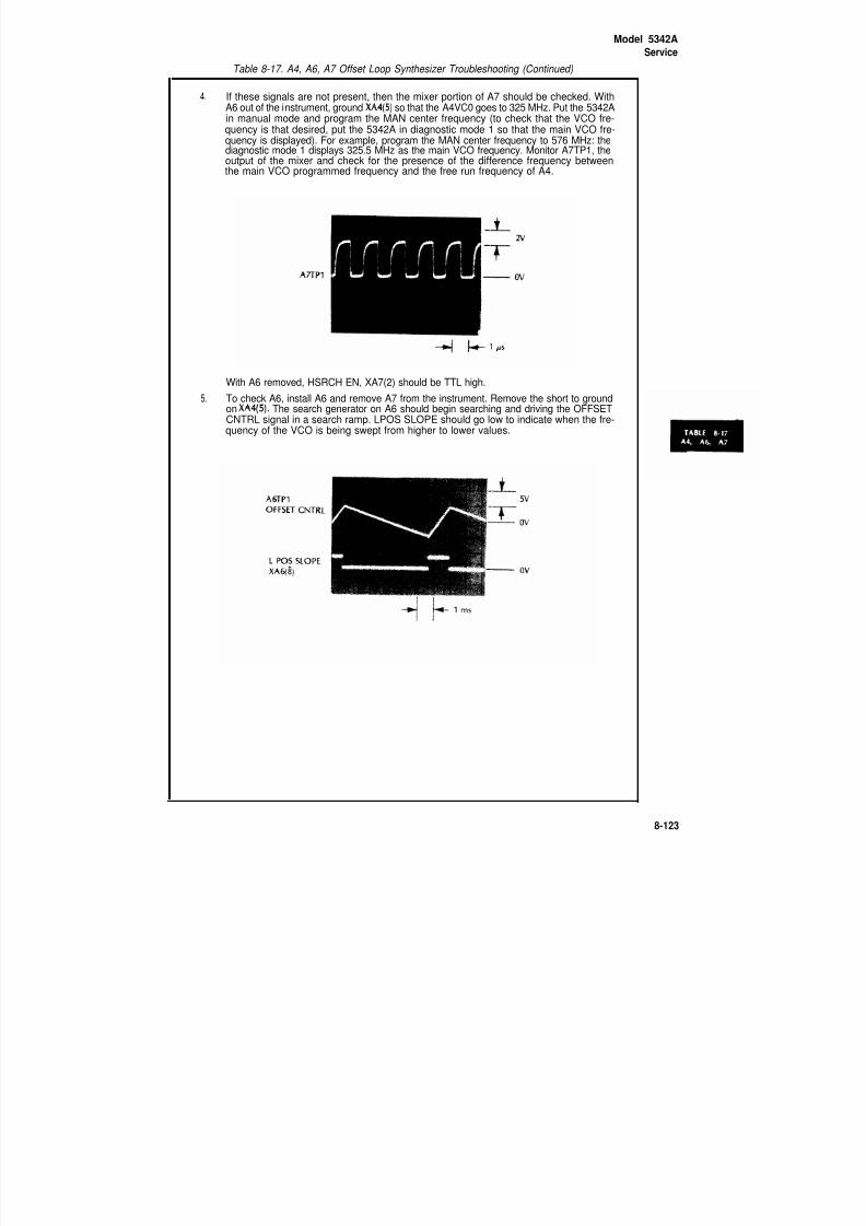
8/21/2019 HP5432 Microwave Frequency Counter
http://slidepdf.com/reader/full/hp5432-microwave-frequency-counter 283/364
TABLE 8-17
Model 5342AService
Table 8-17. A4, A6, A7 Offset Loop Synthesizer Troubleshooting (Continued)
4. If these signals are not present, then the mixer portion of A7 should be checked. WithA6 out of the instrument, ground XA4(5) so that the A4VC0 goes to 325 MHz. Put the 5342Ain manual mode and program the MAN center frequency (to check that the VCO fre-quency is that desired, put the 5342A in diagnostic mode 1 so that the main VCO fre-quency is displayed). For example, program the MAN center frequency to 576 MHz: thediagnostic mode 1 displays 325.5 MHz as the main VCO frequency. Monitor A7TP1, the
output of the mixer and check for the presence of the difference frequency betweenthe main VCO programmed frequency and the free run frequency of A4.
With A6 removed, HSRCH EN, XA7(2) should be TTL high.
5. To check A6, install A6 and remove A7 from the instrument. Remove the short to groundon XA4(5). The search generator on A6 should begin searching and driving the OFFSETCNTRL signal in a search ramp. LPOS SLOPE should go low to indicate when the fre-quency of the VCO is being swept from higher to lower values.
8-123

8/21/2019 HP5432 Microwave Frequency Counter
http://slidepdf.com/reader/full/hp5432-microwave-frequency-counter 284/364
TABLE 8-18
Model 5342A
Service
Table 8-18. A26 Sampler Driver Troubleshooting
1. Remove the U1 Sampler and A26 Sampler Driver as follows:
a. Remove bottom panel by loosening screw at rear, remove two front feet and slide panelrearward.
b. Locate assemblies at bottom front of instrument.
c. Pull off coax cables from A1J1, A1J3, A25J1 (IF OUT INT) and A25J2 (IF OUT EXT).
d. Disconnect rigid coax from U1 Sampler by loosening attaching nut.
e. Remove nut on front panel type N connector and remove rigid cable to allow access.
f. Remove cable strap connector at A22 motherboard and move cable strap to one sideto allow access.
g. Remove 5 screws (four corner and one middle screw) attaching A25 Preamplifier mount-ing bracket and withdraw bracket (and attached assemblies) from instrument.
h. Remove A26 from bracket by removing the two small attaching bolts and nuts. SeparateA26 from U1 by loosening the interconnecting hex connector from U1.
2. Set 5342A to CHECK mode and measure the sampler driver output with a power meter. Theoutput should be greater than +16 dBm (if the output of A5, which is driving A26, is at a levelof approximately +15 dBm).
3. If the A26 output level is good, then A26U1 and associated circuitry are probably functioningproperly. However, a good level does not indicate that the step recovery diode CR1 is working.CRI could be open. To check the diode with an ohmmeter, connect the positive lead of theohmmeter (such as the HP 3465A in OHMS function) to the center conductor of the A26Sampler Driver output and the common leads to the A26 case. Place the ohmmeter in the 2Krange (1 mA current source) and measure a forward resistance of approximately 800 ohms.Measure a reverse resistance of infinity.
4. To replace CR1, simply unscrew the plastic holder and remove CR1 with tweezers. Reversethe process for assembly.
8-124

8/21/2019 HP5432 Microwave Frequency Counter
http://slidepdf.com/reader/full/hp5432-microwave-frequency-counter 285/364
TABLE 8-19
Model 5342AService
Table 8-19. A5 RF Multiplexer Troubleshooting
Set up the test equipment as shown:
Set the 8620C to 1.2 GHz at approximately -20 dBm. Place the 5342A in AUTO, 500 MHz—18 GHzrange, and in diagnostic mode 2 (press SET, SET, 2) so that the counter continuously displays the Acounter contents as it remains in the harmonic determination routine. The trace on the spectrumanalyzer should show two IF’s, indicating that the A5 Multiplexer is switching between the mainsynthesizer and the offset synthesizer.
The wideband filter on A9 is switched in as can be determined by the wider noise skirts about thesignal.
1.2 GHz @ -20 dBm input to CNTR
If the scale is expanded to 1 MHz/div., it is seen that the separation between the IF’s is 2 MHz
(=4 x 500 kHz) where 4 is the N number. Go to diagnostic mode 1 to verify N=4.
8-125
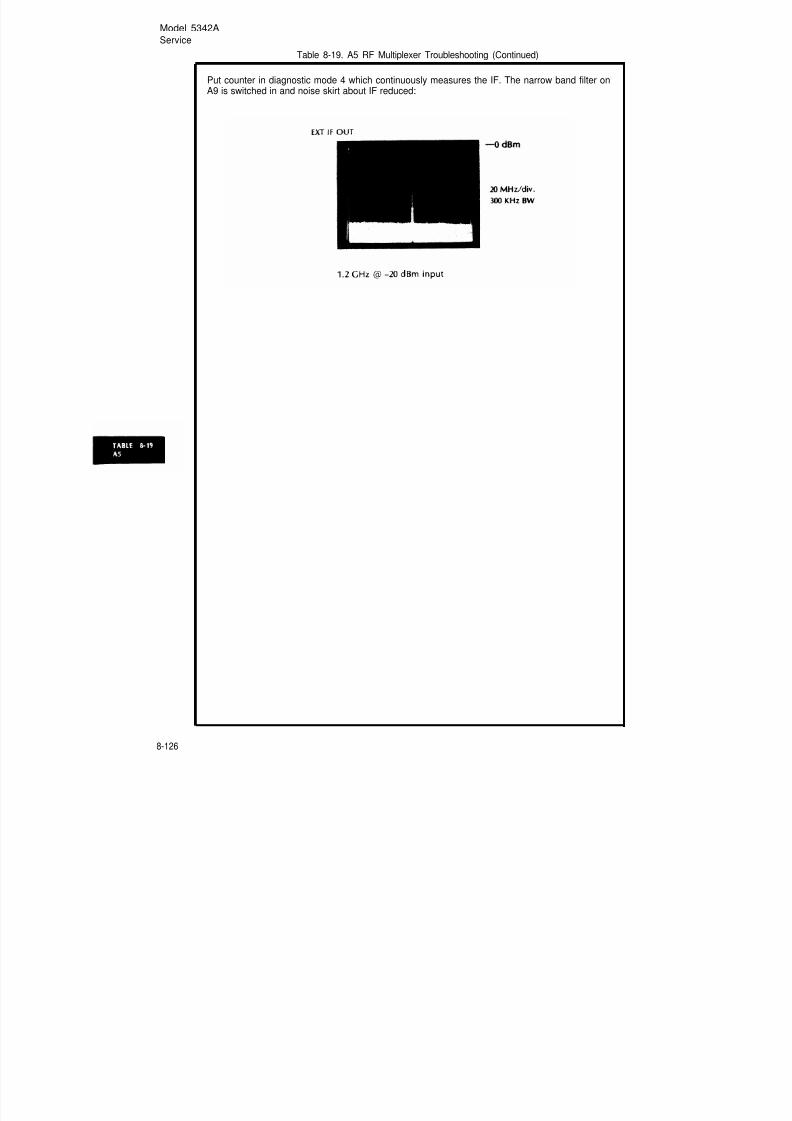
8/21/2019 HP5432 Microwave Frequency Counter
http://slidepdf.com/reader/full/hp5432-microwave-frequency-counter 286/364
TABLE 8-19
Model 5342A
Service
Table 8-19. A5 RF Multiplexer Troubleshooting (Continued)
Put counter in diagnostic mode 4 which continuously measures the IF. The narrow band filter onA9 is switched in and noise skirt about IF reduced:
8-126
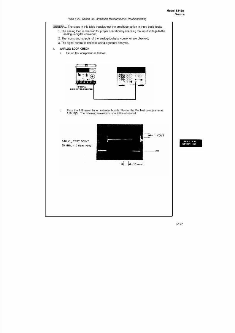
8/21/2019 HP5432 Microwave Frequency Counter
http://slidepdf.com/reader/full/hp5432-microwave-frequency-counter 287/364
TABLEL 8-20
Model 5342AService
Table 8-20. Option 002 Amplitude Measurements Troubleshooting
GENERAL. The steps in this table troubleshoot the amplitude option in three basic tests:
1. The analog loop is checked for proper operation by checking the input voltage to theanalog-to-digital converter;
2. The inputs and outputs of the analog-to-digital converter are checked;
3. The digital control is checked using signature analysis.
1. ANALOG LOOP CHECK
a. Set up test equipment as follows:
b. Place the A16 assembly on extender boards. Monitor the Vin Test point (same asA16U8(5). The following waveforms should be observed:
8-127

8/21/2019 HP5432 Microwave Frequency Counter
http://slidepdf.com/reader/full/hp5432-microwave-frequency-counter 288/364
Model 5342AService
Table 8-20. Option 002 Amplitude Measurements Troubleshooting (Continued)
c. If the input level is increased to 0 dBm, the gain of A16U12 is decreased whichdecreases the level of Vin as follows:
d. If the above waveforms are present, it indicates that the analog loop, consisting ofA27 Low Frequency Amplitude module and the analog portion of A16 circuits arefunctioning properly. To test U2 High Frequency Amplitude module portion ofthe high frequency loop, apply a 500 MHz signal at -10 dBm to the high frequencyinput of the counter (5342A set up for 500 MHz-18 GHz range) and monitor theVin test point. Similar waveforms should be observed.
e. If these waveforms are present, go to step 2, Analog-to-Digital Converter Check.
f. The following steps troubleshoot the analog loop:
(1) Apply a 50 MHz, -10 dBm signal to the low frequency input. Select AMPLand place the 5342A in diagnostic mode 6 (SET, SET 6). With a DVM, measurethe DETECTED RF (LF) input to A16 at A16U18(2).
This voltage should be approximately -0.04 Volts. Increase the input level+10 dBm and measure A16U18(2). This voltage should be approximately-0.70 Volts. If not, check U17(15) for these voltages. If still not present, suspectbad cable or failed A27 Low Frequency Amplitude module.
(2) Apply a 2 GHz, -10 dBm signal to the high frequency input. With the counterin AMPL mode and diagnostic mode 6, measure the DETECTED RF (HF)input to A16 at A16U18(2). This voltage will be approximately -0.03 to-0.04 volts. Increase the input level to +10 dBm and observe a level in therange of approximately -0.6 to -0.7 volts.
8-128

8/21/2019 HP5432 Microwave Frequency Counter
http://slidepdf.com/reader/full/hp5432-microwave-frequency-counter 289/364
Model 5342A
Service
Table 8-20. Option 002 Amplitude Measurements Troubleshooting (Continued)
(3) If the U2 High Frequency Module or the A27 Low Frequency module issuspected, perform the following dc checks using a DVM such as the 3465A.Place the DVM in OHMS function and 2Kfl range (if using a different DVM,select that range which provides a 1 mA constant current). Connect thepositive lead of the DVM to the point indicated by a (+) and the commonlead to the point indicated by a (-).
U2 High Frequency Module Checks
SIGNAL NAME + — OHMMETER
XA16B3 GROUND 950f-1
GROUND XA16m
m
XA16BT
GROUND 950
f-1
GROUND xA16m
m
DETECTED 100 kHz (HF) A16J4* GROUND 2oofl
GROUND A16J4 1.4Kfl
DETECTED-RF (HF) A16J5* GROUND
2oofl
GROUND A1615 1.4Kfl
A27 Low Frequency Module Checks
SIGNAL NAME + — OHMMETER
XA16B4 GROUND 1.2Kfl
GROUND XA16B4 7oofl
DETECTED 100 kHz (LF) A16J3* GROUND 2oofl
GROUND A16J3 1.4Kfl
DETECTED RF (LF) A16J6* GROUND 2oofl
GROUND A16J6 1.4Kfl
Note: *touch center conductor of connector to DVM.
If the U2 High Frequency Module on the A27 Low Frequency Module is sus-pected, perform the following dc checks using a DVM such as the 3465A. Placethe DVM in OHMS function and 2Kfl range (if using a different DVM, selectthat range which provides a 1 mA constant current). Connect the positive leadof the DVM to the point indicated by a (+) and the common lead to the pointindicated by a (—).
(4) Return the counter to normal operating mode by pressing RESET. Apply a50 MHz, -10 dBm signal to the low frequency input. With the counter in AMPLmode, 1 MHz resolution, sample rate full CCW, 50fl and 10 Hz-500 MHz range,observe the following waveforms at the 100 kHz test point (second TP fromright edge of A16 board):
8-129

8/21/2019 HP5432 Microwave Frequency Counter
http://slidepdf.com/reader/full/hp5432-microwave-frequency-counter 290/364
Model 5342AService
Table 8-20. Option 002 Amplitude Measurements Troubleshooting (Continued)
Increase the input level to 0 dBm:
(5) With the 5342A set-up as in step (3), place the 5342A in diagnostic mode 6 andfor a 0 dBm input observe a CW 100 kHz signal at the 100 kHz TP:
(6) To check the switching signals which are sent to the input multiplexer U2and A27, apply a 50 MHz, -10 dBm signal to the low frequency input of the5342A. Place the 5342A in 50fl, 10 Hz-500 MHz range, 1 MHz resolution, samplerate full CCW and AMPL mode. Monitor the AMPL SEL signal at XA16B(4)with an oscilloscope:
8-130
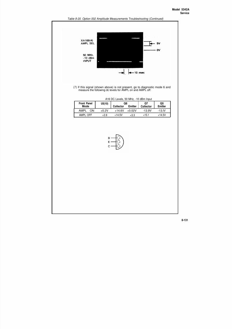
8/21/2019 HP5432 Microwave Frequency Counter
http://slidepdf.com/reader/full/hp5432-microwave-frequency-counter 291/364
Model 5342A
Service
Table 8-20. Option 002 Amplitude Measurements Troubleshooting (Continued)
(7) If this signal (shown above) is not present, go to diagnostic mode 6 andmeasure the following dc levels for AMPL on and AMPL off:
A16 DC Levels, 50 MHz, -10 dBm Input
Front Panel U5(10) Q8 Q7 Q5Mode Collector Emitter Collector Emitter
AMPL ON +0.2V +14.6V +0.02V -13.9V -13.lV
AMPL OFF +3.9 +14.5V +3.3 +15.1 +14.5V
8-131

8/21/2019 HP5432 Microwave Frequency Counter
http://slidepdf.com/reader/full/hp5432-microwave-frequency-counter 292/364
Model 5342A
Service
Table 8-20. Option 002 Amplitude Measurements Troubleshooting (Continued)
(8) Apply a -10 dBm, 500 MHz signal to the 500 MHZ-18 GHz input and press RESET.Set the 5342A to 1 MHz resolution, AMPL on, and the 500 MHz-18 GHz_range.Check the AMPL ON signal at XA16B(4) and the FREQ ON signal at XA16B(3) withan oscilIoscope:
(9) If the waveforms (shown above) are not present, go to diagnostic mode 6 andcheck the voltages in the following table:
A16 DC LEVELS, 500 MHz, -10 dBm INPUT
Mode U5(10) U5(11) Q 5 Q 9 Q 6 Q 4 Q 1 Q 2Emitter
AMPL +0.2 +3.4 -13.1 +4.97C +0.07C +4.99C +0.05C +0.05CON +4.2B +0.7B +0.07B +5.0B +5.0B
AMPL +3.9 +0.2 +14.5 +0.01C +4.8C +0.07C +5.OC +5.0BOFF +4.98B +0.16B +0.7B +4.4B +4.3B
Note: C = Collector, B = BaseNOTE
For amplitudes greater than approximately +5 dBm at the high fre-quency input, the ATT signal at XA16B(3) changes from +7(tl) volts(low levels) to O(tl) volts (high levels). To verify proper operation,apply a 500 MHz, -10 dBm signal to the 5342A high frequency inPut.Select AUTO and AMPL off. Increase the input level while monitoringXA16B(3) on the ATT test point with a DVM. Decrease input level untilATT goes to
+7(f)
volts again. The input signal level where this occursshould be around 1-2 dB less than the level which originally causedATT to go low.
8-132

8/21/2019 HP5432 Microwave Frequency Counter
http://slidepdf.com/reader/full/hp5432-microwave-frequency-counter 293/364
Model 5342A
Service
Table 8-20. Option 002 Amplitude Measurements Troubleshooting (Continued)
2. ANALOG-TO-DIGITAL CONVERTER CHECK
a. Using DVM, measure the following voltage points:
(1) Check the 10 volt reference at the +10V TP (or A16U8(3) for 10.00 volts.
(2) Check the 6.6V TP (or A16U8(7) ) for 6.64V DC.
(3) Check the 3.2V TP (or A16U8(8)) for 3.20V DC.
b. Apply a 50 MHz, -10 dBm signal to the 5342A low frequency input. Set the 5342Ato
500,
10 Hz-500 MHz range, 1 MHz resolution, sample rate full CCW, and AMPLmode. Monitor U5(6) and the start conversion signal at U5(3) with an oscilloscope:
CAUTION
U8 is a large-scale MOS integrated circuit. Its inputs are susceptible todamage by high voltage and static charges. Particular care shouldbe exercised when servicing this circuit or handling it under condi-tions where static charges can build up.
c. With the counter set up as in step b, monitor the conversion complete signal atU6(10) and U8(6). Since U6(10) also receives data, the signal at U6(10) may vary asshown in the following two scope photos. In the first photo, the data is high afterthe conversion complete goes low (true). In the second photo, the data is lowafter the conversion complete goes low.
8-133

8/21/2019 HP5432 Microwave Frequency Counter
http://slidepdf.com/reader/full/hp5432-microwave-frequency-counter 294/364
Model 5342AService
Table 8-20. Option 002 Amplitude Measurements Troubleshooting (Continued)
8-134
3. DIGITAL CHECK
a. Place the A16 assembly on a 10- and an 18-pin extender board (05342-60030 and
05324-60033). Set switches S1 and S2 on the A14 Microprocessor assembly to theCount Mode as shown below.
Normal Mode
Count Mode (for use with 5004A Signature Analyzer)
b. Connect 5004A Signature Analyzer START and STOP probes to A16U1(4), theCLOCK probe to VMA02 test pin on the A14 assembly and the GND probe to testpin on the A14 assembly. Set the 5004A front panel switches as follows:

8/21/2019 HP5432 Microwave Frequency Counter
http://slidepdf.com/reader/full/hp5432-microwave-frequency-counter 295/364
Model 5342AService
Table 8-20. Option 002 Amplitude Measurements Troubleshooting (Continued)
Signatures on PROM U4 should be as follows:
Signal Name Location Signature
LAO
U4(8) A872LA1 U4(7) 2068LA2 U4(6) 335HLA3 U4(5) 0F51LA4 U4(4) C177LA5 U4(3) U929LA6 U4(2) 3032LA7 U4(1) HU4ULA8 U4(23) 9CC8LA9 U4(22) 5F08LA10 U4(19) U81PLA11 U4(20) 0000
U4(9) 1U2FU4(10) 7471U4(11) H412U4(13) 59U1U4(14) 512PU4(15) 60HAU4(16) 7463U4(17) 85C8
c. Connect the 5004A Signature Analyzer START and STOP probes to A16U9(8) (testpin labeled $3) on A16 assembly, the CLOCK probe to VMA 02 test pin on the A14assembly and the GND probe to test pin on the A14 assembly. Set the 5004A frontpanel switches as follows:
d. Remove PROM A16U3 from its socket. Signatures on A16U6 and U7 should beas follows:
Signal Name Location Signature
H READ ADC U6(1) 0000L READ U6(15) 0000U6(2) 733U
DB4/DB12 U6(3) 0000U6(5) U110
DB5 U6(6) 0000U6(11) HHH8
DB7/BUSY U6(10) 0000U6(14) 8UUH
DB6/OVERRANGE U6(13) 0000H READ ADC U7(1) 0000L READ U7(15) 0000
U7(2) UFU5DBwDB8
U7(3) 0000U7(5) P9A7
DB1/DB9 U7(6) 0000
U7(11) 2045DB3/DB11 U7(10) 0000
U7(14) 6C72DB2/DB10 U7(13) 0000LDO
U7(4) 9FFULD1 U7(7) 899HLD2 U7(12) 0C48LD3 U7(9) 407ULD4 U6(4) 1305LD5 U6(7) 912ALD6 U6(12) PUF7LD7 U6(9) CHP2
8-135

8/21/2019 HP5432 Microwave Frequency Counter
http://slidepdf.com/reader/full/hp5432-microwave-frequency-counter 296/364
Model 5342A
Service
Table 8-20. Option 002 Amplitude Measurements Troubleshooting (Continued)
8-136
e. Connect the 5004A Signature Analyzer START and STOP probes to A16U9(1), theCLOCK probe to VMA02 test pin on the A14 assembly and the GND probe totest pin on the A14 assembly. Set the 5004A front panel switches as follows:
f. Observe the following signatures:
+5V 0003 (Characteristic High Signature)
Pin Signature Pin Signature
Ul(l) 854F U9(1) 0002(2) 854U (2) 9UP2(3) 6U2C (3) 0003(4) 6U28 (4) 0003
(5) 0003
(6) 0003U2(1) 6114 (8) 854F
(2) 486C (9) —
(3) 4FC9 (10) —
(4) C91U (11) 6114(5) 3F53 (12) 0003(6) 854U(8) 3F50(9) 0003
(10) 0000(11) 3F50(12) 0000(13) 3F53

8/21/2019 HP5432 Microwave Frequency Counter
http://slidepdf.com/reader/full/hp5432-microwave-frequency-counter 297/364
Model 5342A
Service
Table 8-21. Option 011 HP-IB Troubleshooting
Table 8-21A. Acceptor Handshake (HP-IB)
8-137

8/21/2019 HP5432 Microwave Frequency Counter
http://slidepdf.com/reader/full/hp5432-microwave-frequency-counter 298/364
Model 5342A
Service
Table 8-21. Option 077 HP-IB Troubleshooting (Continued)
2.
a.
b.
Source Handshake Troubleshooting
Setup:
HP-IB CABLE
5342A
Set rear panel addressswitch to Talk only:
59401ABUS SYSTEMANALYZER
59401A settings:
REN true (REN light ON)
HALT
LISTEN mode
Remove the A14 Microprocessor assembly. Perform the actions listed in Table 8-21B to verify thesource handshake. Use a 546A Logic Pulser to clock circuit nodes and a 545A Logic Probe tocheck the state of circuit nodes.
Table 8-21B. Source Handshake (HP-IB)
59401 A
STEP ACTION DAV NRFD NDACLight Light Light U5(4) U9(9) U2(4) U2(13) U4(9) U5(13) U4(5) U36(3)
0 Apply power to 5342A OFF OFF ON H igh High Low Low High Low Low High
1 Clock U9(11) once OFF OFF ON High Low High Low High Low Low High
2 Clock U4(11) once OFF OFF ON High Low High High Low Low Low High
3 Clock U4(11) once ON OFF ON High Low Low High Low Low High Low
4 Press EXECUTE on 59401A ON ON OFF High Low Low Low Low Low High Low
5 Clock U4(11) once OFF OFF ON Low High Low Low High Low High High
6 Clock U4(11) once OFF OFF ON High High Low Low High Low Low High
7 Go to Step 1 and the Hand-shake Sequence Repeats
8-138

8/21/2019 HP5432 Microwave Frequency Counter
http://slidepdf.com/reader/full/hp5432-microwave-frequency-counter 299/364
Model 5342A
Service
Table 8-21, Option 011 HP-1B Troubleshooting (Continued)
3. U23, U26 ROM Troubleshooting
a. Setup:
HP-IB CABLE
5342A 59401ABUS SYSTEM
Set rear panel address ANALYZERswitch to:
59401A settings:
MEMORY . . . . OFF
COMP . . . .. OFFTALK Mode
HALT
SRQ = O, EOI = O
REN True
b. Remove the A14 Microprocessor assembly from the 5342A. Place A15 HP-IB assembly on anextender. Place an AP clip on U1 and ground U1(8). Set ATN and the DIO switches on the 59401Aas listed in Table 8-21C and check with a 545A Logic Probe for the correct outputs.
Table 8-21C. U23, U26 ROM Table (HP-1B)
COMMENTS**59401A SETTINGS
DIO LINES *U23 PINS *U26 PINS
ATN 8 7 6 5 4 3 2 1 1 2 3 4 5 6 7 1 2 3 4 5 6 7 8 9
Listen Address 1 0 0 1 0 0 0 0 0
Talk Address 1 0 1 0 0 0 0 0 0
Data (M) 0 0 1 0 0 1 1 0 1
1 0 1 1 1 1 1
0 1 1 1 1 1 1
1 1 1 1 0 0 1
1 0 1 0 0 0 0 0 0
1 0 1 0 0 0 0 0
1 0 1 0 0 0 0 0
Go to Local 1 0 0 0 0 1 1 1 0 0 1 0 1 1 0 1 1 1 0 1 0
Serial Poll Enable 1 0 0 0 1 1 0 0 0 1 1 0 1 1 1 1 1 1 1 0 0 0 0 0 1
Serial Poll Disable 1 0 0 0 1 1 0 0 1
Group Execute Trigger 1 0 0 0 0 1 0 0 0
1 1 0 1 1 1 1
1 1 0 0 1 0 1
1 1 0 0 1 0 1
1 0 0 0 0 0 0 0
1 0 1 1 0 0 1 0
1 0 1 1 1 1 1 1 0 Local Lock-Out 1 0 0 0 1 0 0 0 1
Device Clear 1 0 0 0 1 0 1 0 0
Selected Device Clear 1 0 0 0 0 0 1 0 0
1 1 0 0 1 0 1 1 0 1 0 1 1 1 0
1 1 0 0 1 0 1
Unlisten 1 0 0 1 1 1 1 1 1
Untalk 1 0 1 0 1 1 1 1 1
NOTES:*Ground U1(8) to enable ROM U23*1 = TTL High for U23, U26
**(1 = TTL LOW for 59401 A outputs, e.g., if DIO7 set to 1,
1 0 1 1 1 1 1
1 0 1 0 1 0 1 0
0 0 1 0 0 0 0 0
0 0 1 0 0 0 0 00 1 1 1 1 1 1
then LDIo7 at A15U31(10) is TTL Low)
8-139

8/21/2019 HP5432 Microwave Frequency Counter
http://slidepdf.com/reader/full/hp5432-microwave-frequency-counter 300/364
Model 5342AService
Table 8-21. Option 011 HP-IB Troubleshooting (continued)
4. Troubleshooting Registers U27, U24, U21, U16, U18, U30, U15
a. Setup:
HP-IB CABLE
5342A 59401 ABUS SYSTEMANALYZER
b. Remove A14 Microprocessor assembly from the 5342A and place the A15 HP-IB assembly onextender boards.
c. Place an AP clip on U11 and connect a clip lead from U11(12) to ground. This enables the U27Data In register.
d. U27 CHECK:
Set the 59401A to TALK, HALT, and the 8 DIO switches to 0 (all switches down). Check the inputsto U27(3, 4, 7, 8, 13, 14, 17, 18) for all TTL high. If these inputs are not all TTL high, troubleshoot theinput data buffers U22, U25, U31. With the 546A Logic Pulser, pulse U27(11). Check the outputsof U27(2, 5, 6, 9, 12, 15, 16, 19) for all TTL high. Change the DIO switches of the 59401A to all 1 (allswitches up). Pulse U27(11) once. Check the U27 outputs for all TTL low.
e. U21 CHECK:
If U27 is working, it is possible to control the state of the microprocessor data bus and therebycheck out U21, U24, and U16. To checkout U21, ground U12(5) with another clip lead (U12(12) isstill grounded). This enables U21. With the 59401A DIO switches all set to 1 (all switches up),clock U27(11) with the Logic Pulser. Now clock U21(11). Check the outputs of U21(2, 5, 6, 9, 12,15, 16, 19) for all TTL low. Now change all the 59401A DIO switches to 0 (all switches down). ClockU27(11) with the Logic Pulser. Verify that the U21 outputs are still TTL low. Now clock U21(11).Verify that the U21 outputs are all high.
f. U24 CHECK:
Change the clip lead on U12 from pin 5 to pin 13 so that U12(13) is grounded. Check that U21(1) isTTL high. If U21(1) remains low after the clip lead is removed, the serial poll FF U29 must be sethigh. To do this, ground U29(14) and clock U29(12). Verify that U29(10) is TTL high. U12(13)grounded enables U24. U27 should still be enabled by the ground on U11(12). With the 59401A
DIO switches all set to 0 (switches down), clock U27(11) and clock U24(11). Verify that the out-puts of U24(2, 5, 6, 9, 12, 15, 16, 19) are all TTL high. Change the 59401A DIO switches to 1 (all
switches up). Clock U27(11) with the Logic Pulser. Verify that all the U24 outputs are still TTLhigh. Now clock U24(11) and verify that the U24 outputs are all TTL low.
g. U16 CHECK:
Remove the clip lead from U12(13). U27 should still be enabled by the ground on U11(12). Withthe DIO switches of the 59401A all set to 1 (all switches up), clock U27(11) with the 546A LogicPulser. Next clock U16(9) and verify that the outputs of U16(2, 5, 7, 10, 12, 15) are all TTL low.Change the DIO switches on the 59401A to 0 (all switches down) and clock U27(11). Verify thatU16 outputs remain TTL low. Now clock U16(9) and verify that the U16 outputs are all TTL high.
8-140

8/21/2019 HP5432 Microwave Frequency Counter
http://slidepdf.com/reader/full/hp5432-microwave-frequency-counter 301/364
Model 5342AService
Table 8-21. Option 011 HP-iB Troubleshooting (Continued)
h. U18 CHECK:
Change the clip lead on U11 from pin 12 to pin 13 so that U11(13) is now grounded. This actionwill disable the U27 Data In register and will enable the U18 Interrupt Out register. Clock eachof the inputs to U18(2, 4, 6, 10, 12) with a 546A Logic Pulser, and simultaneously check the corre-sponding output, U18(3, 5, 7, 9, 11) with the 545A Logic Probe. Remove the ground from U11(13)
and verify that clocking an input has no effect upon an output (all the outputs should be in thehigh Z state).
i. U30 CHECK:
Change the ground to U11(15) with the clip lead. This enables the State In register U30. Clockeach of the inputs to U30(2, 6, 10, 12, 14) and simultaneously check the corresponding outputs ofU30(3, 7, 9, 11, 13). Remove the ground from U11(15) and verify that clocking an input has noeffect upon an output.
j. U15 CHECK:
Change the ground to U11(14) which enables the Command In register U15. Set the DIOswitches and ATN to the following:A T N 8 7 6 5 4 3 2 1
1 0 0 1 0 0 0 0 0(5342A rear panel HP-IB address switches set to 00001)
This should cause the U26 ROM outputs to present a TTL low to U15(12, 13, 14). Verify this with a
logic probe. U15(11) will be TTL high since the A15 assembly powers up with the U20 Listen FFreset.
Clock U15(7) with the Logic Pulser and verify that U15(3, 4, 5) are TTL low and U15(6) is TTL high.
Set the DIO switches to the following:
A T N 8 7 6 5 4 3 2 10 0 1 0 0 0 0 1
Clock U20(12) to set the U20 Listen FF. This causes U15(11) to go TTL low.
Now set the DIO switches to the following:
A T N 8 7 6 5 4 3 2 11 0 0 0 1 0 0 0 1
This causes the U26 ROM outputs to present a TTL high to U15(12, 13, 14). Verify this with thelogic probe. U15(11) should beTTL low. Clock U15(7) and verify that U15(3,4, 5) are TTL high and
U15(6) is TTL low.
1
8-141

8/21/2019 HP5432 Microwave Frequency Counter
http://slidepdf.com/reader/full/hp5432-microwave-frequency-counter 302/364
Model 5342A
Service
Part of Figure 8-19. 5342A Front (A1 Display) View
8-142

8/21/2019 HP5432 Microwave Frequency Counter
http://slidepdf.com/reader/full/hp5432-microwave-frequency-counter 303/364
Model 5342A
Service
Figure 8-20. 5342A Rear View
8-143

8/21/2019 HP5432 Microwave Frequency Counter
http://slidepdf.com/reader/full/hp5432-microwave-frequency-counter 304/364
Model 5342A
Service
Figure 8-21. 5342A Top View (Assembly Locations and Adjustments)8-144

8/21/2019 HP5432 Microwave Frequency Counter
http://slidepdf.com/reader/full/hp5432-microwave-frequency-counter 305/364
Model 5342A
Service
Figure 8-22. 5342A Bottom View, Options Installed
8-145/ (8-146 blank)

8/21/2019 HP5432 Microwave Frequency Counter
http://slidepdf.com/reader/full/hp5432-microwave-frequency-counter 306/364
Fg u

8/21/2019 HP5432 Microwave Frequency Counter
http://slidepdf.com/reader/full/hp5432-microwave-frequency-counter 307/364
Model 5342A
Service
A2
Par t of F i gur e 8- 24. A l D i spl ay Assembl y and A2 D i spl ay Dr i ve Assembl y
8-148

8/21/2019 HP5432 Microwave Frequency Counter
http://slidepdf.com/reader/full/hp5432-microwave-frequency-counter 308/364

8/21/2019 HP5432 Microwave Frequency Counter
http://slidepdf.com/reader/full/hp5432-microwave-frequency-counter 309/364
Fg u e 8 2 5

8/21/2019 HP5432 Microwave Frequency Counter
http://slidepdf.com/reader/full/hp5432-microwave-frequency-counter 310/364
Model 5342A
Service
Part of Figure 8-26. A3 Direct Count Amplifier Assembly
8-152

8/21/2019 HP5432 Microwave Frequency Counter
http://slidepdf.com/reader/full/hp5432-microwave-frequency-counter 311/364
Fg u e 8 2 6

8/21/2019 HP5432 Microwave Frequency Counter
http://slidepdf.com/reader/full/hp5432-microwave-frequency-counter 312/364
8154
Fg u e 8 2 7

8/21/2019 HP5432 Microwave Frequency Counter
http://slidepdf.com/reader/full/hp5432-microwave-frequency-counter 313/364
F

8/21/2019 HP5432 Microwave Frequency Counter
http://slidepdf.com/reader/full/hp5432-microwave-frequency-counter 314/364
Model 5342A
Service
.
COMPONENT SIDE
SOLDER SIDE
Part of Figure 8-28. A5 RF Mult iplexer Assembly
8-156

8/21/2019 HP5432 Microwave Frequency Counter
http://slidepdf.com/reader/full/hp5432-microwave-frequency-counter 315/364
Fg

8/21/2019 HP5432 Microwave Frequency Counter
http://slidepdf.com/reader/full/hp5432-microwave-frequency-counter 316/364
Model 5342A
Service
.
Part of Figure 8-29. A6 Offset Loop Amp/Search Generator Assembly

8/21/2019 HP5432 Microwave Frequency Counter
http://slidepdf.com/reader/full/hp5432-microwave-frequency-counter 317/364
Fg u e 8 2 9

8/21/2019 HP5432 Microwave Frequency Counter
http://slidepdf.com/reader/full/hp5432-microwave-frequency-counter 318/364
Fg u e 8 3 0
8160

8/21/2019 HP5432 Microwave Frequency Counter
http://slidepdf.com/reader/full/hp5432-microwave-frequency-counter 319/364
Fg u e 8 3 0

8/21/2019 HP5432 Microwave Frequency Counter
http://slidepdf.com/reader/full/hp5432-microwave-frequency-counter 320/364
Model 5342AService
Part ot f igure 8-37. A8 Mai n VCO Assembl y
8-162

8/21/2019 HP5432 Microwave Frequency Counter
http://slidepdf.com/reader/full/hp5432-microwave-frequency-counter 321/364
Fg u

8/21/2019 HP5432 Microwave Frequency Counter
http://slidepdf.com/reader/full/hp5432-microwave-frequency-counter 322/364
8164
Fg u e 8 3 2

8/21/2019 HP5432 Microwave Frequency Counter
http://slidepdf.com/reader/full/hp5432-microwave-frequency-counter 323/364
Fg u e 8 3 2 A

8/21/2019 HP5432 Microwave Frequency Counter
http://slidepdf.com/reader/full/hp5432-microwave-frequency-counter 324/364
Model 5342A
Service
.
8-166
Part of Figure 8-33. A10 Divide-by-N Assembly

8/21/2019 HP5432 Microwave Frequency Counter
http://slidepdf.com/reader/full/hp5432-microwave-frequency-counter 325/364
Fg u e 8 3 3

8/21/2019 HP5432 Microwave Frequency Counter
http://slidepdf.com/reader/full/hp5432-microwave-frequency-counter 326/364
Model 5342A
Service
..
.
Part of Figure 8-34. A11 IF Limiter Assembly
8-168

8/21/2019 HP5432 Microwave Frequency Counter
http://slidepdf.com/reader/full/hp5432-microwave-frequency-counter 327/364
F

8/21/2019 HP5432 Microwave Frequency Counter
http://slidepdf.com/reader/full/hp5432-microwave-frequency-counter 328/364
8170
Model 5342A
Service
Part of Figure 8-35. A12 IFDetector Assembly

8/21/2019 HP5432 Microwave Frequency Counter
http://slidepdf.com/reader/full/hp5432-microwave-frequency-counter 329/364
Fg u e

8/21/2019 HP5432 Microwave Frequency Counter
http://slidepdf.com/reader/full/hp5432-microwave-frequency-counter 330/364
Model 5342A
Service
I
Part of Figure 8-36. A13 Counter Assembly
8-172

8/21/2019 HP5432 Microwave Frequency Counter
http://slidepdf.com/reader/full/hp5432-microwave-frequency-counter 331/364

8/21/2019 HP5432 Microwave Frequency Counter
http://slidepdf.com/reader/full/hp5432-microwave-frequency-counter 332/364

8/21/2019 HP5432 Microwave Frequency Counter
http://slidepdf.com/reader/full/hp5432-microwave-frequency-counter 333/364

8/21/2019 HP5432 Microwave Frequency Counter
http://slidepdf.com/reader/full/hp5432-microwave-frequency-counter 334/364

8/21/2019 HP5432 Microwave Frequency Counter
http://slidepdf.com/reader/full/hp5432-microwave-frequency-counter 335/364

8/21/2019 HP5432 Microwave Frequency Counter
http://slidepdf.com/reader/full/hp5432-microwave-frequency-counter 336/364

8/21/2019 HP5432 Microwave Frequency Counter
http://slidepdf.com/reader/full/hp5432-microwave-frequency-counter 337/364

8/21/2019 HP5432 Microwave Frequency Counter
http://slidepdf.com/reader/full/hp5432-microwave-frequency-counter 338/364

8/21/2019 HP5432 Microwave Frequency Counter
http://slidepdf.com/reader/full/hp5432-microwave-frequency-counter 339/364
Figure 8-40. Option 003 A16 Extended Dynamic Range Assembly
8-181
8/21/2019 HP5432 Microwave Frequency Counter
http://slidepdf.com/reader/full/hp5432-microwave-frequency-counter 340/364
Model 5342A
Service
Part of Figure 8-41, A17 Timing Generator Assembly
8-182

8/21/2019 HP5432 Microwave Frequency Counter
http://slidepdf.com/reader/full/hp5432-microwave-frequency-counter 341/364
Fg u e 8

8/21/2019 HP5432 Microwave Frequency Counter
http://slidepdf.com/reader/full/hp5432-microwave-frequency-counter 342/364
Fg u e 8 4 2
8184

8/21/2019 HP5432 Microwave Frequency Counter
http://slidepdf.com/reader/full/hp5432-microwave-frequency-counter 343/364
Fg u e 8 4 2

8/21/2019 HP5432 Microwave Frequency Counter
http://slidepdf.com/reader/full/hp5432-microwave-frequency-counter 344/364
Fg u e 8 4 3
8-186

8/21/2019 HP5432 Microwave Frequency Counter
http://slidepdf.com/reader/full/hp5432-microwave-frequency-counter 345/364

8/21/2019 HP5432 Microwave Frequency Counter
http://slidepdf.com/reader/full/hp5432-microwave-frequency-counter 346/364

8/21/2019 HP5432 Microwave Frequency Counter
http://slidepdf.com/reader/full/hp5432-microwave-frequency-counter 347/364
F

8/21/2019 HP5432 Microwave Frequency Counter
http://slidepdf.com/reader/full/hp5432-microwave-frequency-counter 348/364
Fg u e 8 4 5
8-190

8/21/2019 HP5432 Microwave Frequency Counter
http://slidepdf.com/reader/full/hp5432-microwave-frequency-counter 349/364
Fg

8/21/2019 HP5432 Microwave Frequency Counter
http://slidepdf.com/reader/full/hp5432-microwave-frequency-counter 350/364
Model 5342A
Service
.
\
Part of Figure 8-46. A26 Sampler Driver Assembly
8-192
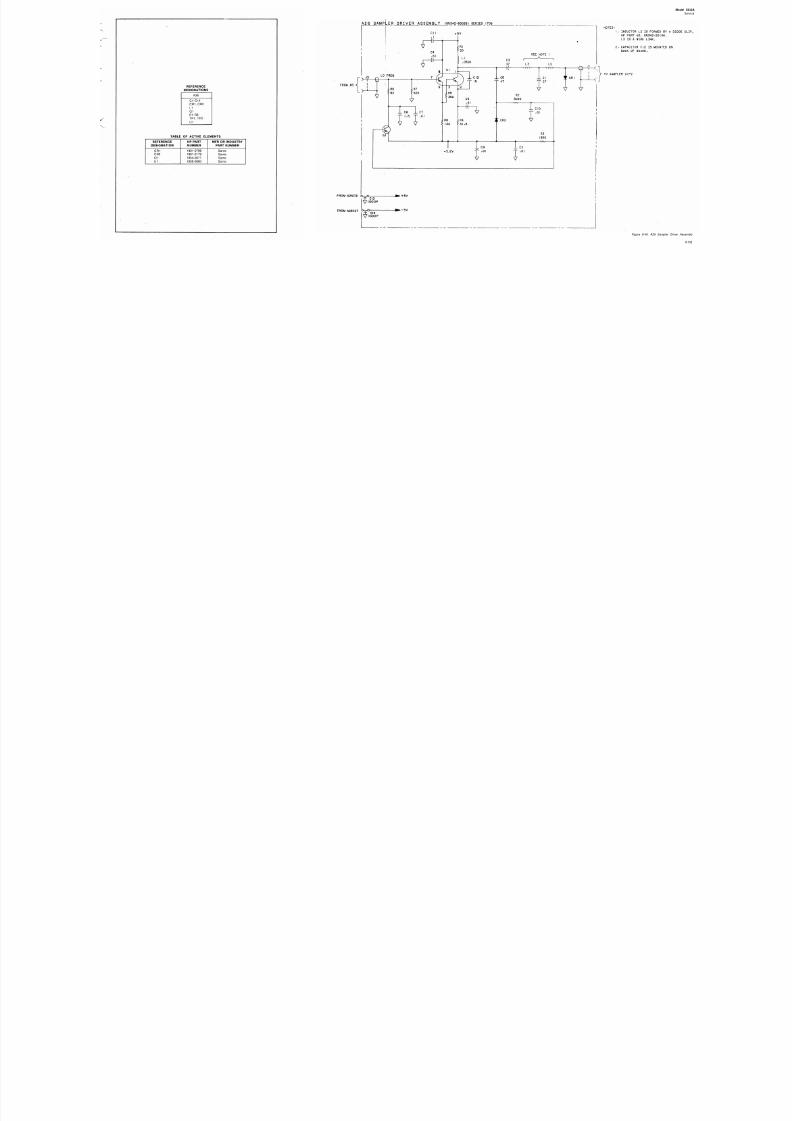
8/21/2019 HP5432 Microwave Frequency Counter
http://slidepdf.com/reader/full/hp5432-microwave-frequency-counter 351/364
Figure 8-46. A26 Sam

8/21/2019 HP5432 Microwave Frequency Counter
http://slidepdf.com/reader/full/hp5432-microwave-frequency-counter 352/364
8-194
8/21/2019 HP5432 Microwave Frequency Counter
http://slidepdf.com/reader/full/hp5432-microwave-frequency-counter 353/364
EUROPE, NORTH AFRICA AND MIDDLE EAST
8-195/(8-196 blank)

8/21/2019 HP5432 Microwave Frequency Counter
http://slidepdf.com/reader/full/hp5432-microwave-frequency-counter 354/364
TM 11-6625-3014-14
APPENDIX A
REFERENCES
DA Pam 310.4
SB 38-100
TB 43-180
TB 43-0118
TM 11-6625-539-14-3
TM 11-6625-2780-14&P
TM 11-6625-2964-14&P
TM 38-750
TM 740-90-1
TM 750-244-2
Index of Technical publications.
Preservation, Packaging, Packing and MarkingMaterials, Supplies, and Equipment Used bythe Army.
Calibration Requirements for the Maintenance ofArmy Materiel.
Field instructions for painting and preservingElectronics Command equipment, includingcamouflage pattern painting of electrical
equipment shelters.
Operator’s, Organizational, Direct Support andGeneral Support Maintenance Manual: Test Set,Transistor TS-1836C/U (NSN 6625-00-159-2263)Changes 1, 2.
Operator’s, Organizational, Direct Support, andGeneral Support Maintenance Manual, IncludingRepair Parts and Special Tools Lists for SignalGenerators SG-ll12(V)l/U and SG-1l12(V)2/U,(Hewlett-Packard Model 8640B, Options 001 and
OO4)(NSN 6625-00-566-3067), SG-ll12(V)l/U,(NSN 6625-00-500-6525) SG-1112(V)2/U.
Operator’s, Organizational, Direct Support andGeneral Support Maintenance Manual (IncludingRepair Parts and Special Tools Lists) for DCPower Supply PP-7547/U (Hewlett-Packard Model6113A) (NSN 6130-00-225-1 682)
The Army Maintenance Management System (TAMMS).
Administrative Storage of Equipment.
Procedures for Destruction of electronicsMateriel to Prevent Enemy Use.
A-1/(A-2 blank)

8/21/2019 HP5432 Microwave Frequency Counter
http://slidepdf.com/reader/full/hp5432-microwave-frequency-counter 355/364
APPENDIX B
TM 11-6625-3014-14Model 5342A
MAINTENANCE ALLOCATION
Section I. INTRODUCTION
B-1. General
This appendix provides a summary of the main-tenance operations for the TD-1225A(V)/U. Itauthorizes categories of maintenance for specificmaintenance functions on repairable items andcomponents and the tools and equipment requiredto perform each function. This appendix maybe used as an aid in planning maintenance opera-
tions.
B-2. Maintenance Function
Maintenance functions will be limited to and de-fined as follows:
a. Inspect. To determine the serviceability of anm by comparing its physical, mechanical, and/
or electrical characteristics with established stand-ards through examination.
b. Test. To verify serviceability and to detectincipient failure by measuring the mechanical or
electrical characteristics of an item and compar-ing those characteristics with prescribed stand-ards.
c. Service. Operations required periodically to keep an item in proper operating conditions, i.e.,
to clean (decontaminate), to preserve, to drain,to paint, or to replenish fuel, lubricants, hydraulicfluids, or compressed air supplies.
d. Adjust To maintain, within prescribed limits,by bringing into proper or exact position, or bysetting the operating characteristics to the speci-fied parameters.
e. Align. To adjust specified variable elementsan item to bring about optimum or desired
performance.
f. Calibrate. To determine and cause correctionsto be made or to be adjusted on instruments or
t measuring and diagnostic equipments used
in precision measurement. Consists of compari.sons of two instruments, one of which is a certifiedstandard of known accuracy, to detect and adjustany discrepancy in the accuracy of the instrumentbeing compared.
g. Install. The act of emplacing, seating, or fix-ing into position an item, part, module (compo-nent or assembly) in a manner to allow the proper
functioning of the equipment or system. h. Replace. The act of substituting a serviceable
like type part, subassembly, or module (componentor assembly) for an unserviceable counterpart,.
i. Repair. The application of maintenance serv-ices (inspect, test, service, adjust, align, calibrate,replace) or other maintenance actions (welding,grinding, riveting, straightening, facing, rema-chining, or resurfacing) to restore serviceabilityto an item by correcting specific damage, fault,malfunction, or failure in a part, subassembly,module (component or assembly), end item orsystem.
j. Overhaul. That maintenance effort (service/ action) necessary to restore an item to a complete-ly serviceable/operational condition as prescribedby maintenance standards (i.e., DMWR) in appro-priate technical publications. Overhaul is normallythe highest degree of maintenance performed bythe Army. Overhaul does not normally return anitem to like new condition.
k. Rebuild. Consists of those services actionsnecessary for the restoration of unserviceable
equipment to a like new condition in accordancewith original manufacturing standards. Rebuildis the highest degree of materiel maintenanceapplied to Army equipment. The rebuild operationincludes the act of returning to zero those agemeasurements (hours, miles, etc.) considered inclassifying Army equipments/components.
B-1

8/21/2019 HP5432 Microwave Frequency Counter
http://slidepdf.com/reader/full/hp5432-microwave-frequency-counter 356/364
TM 11 6625-3014-14
Model 5342A
B-3. Column Entriesa. Column 1, Group N umber. Column 1 lists
group numbers, the purpose of which is to identifycomponents, assemblies, subassemblies, and mod-ules with the next higher assembly.
b. Column 2, Component / Assembl y.Column 2conta ins th e noun na mes of component a ssem-
blies, subassemblies, and modules for which main-tenance is authorized.
c. Column 8, Mai nt enan ce Functi ons. Column 3lists the functions to be performed on the itemlisted in column 2. When items are listed withoutma int ena nce functions, it is solely for purposeof having th e group numbers in the MAC a ndRP STL coincide.
d. Colum n 4, Maint enance Category. Column 4specifies, by the listing of a “worktime” figure inthe appropriate subcolumn (s), the lowest level ofmaintenance authorized to perform the functionlisted in column 3. This figure represents the ac-t ive t ime required to perform t ha t ma intena ncefunction at the indicated category of maintenance.I f t he number or complexity of the ta sks w ithinthe listed maintenance function vary at differentmaintenance categories, appropriate “worktime”figures will be shown for each category. The num-ber of task-hours specified by the “worktime”f igure represents the average time required torestore an item (assembly, subassembly y, compo-nent, module, end item or system) to a serviceable
condition under typical field operating conditions.This time includes preparation time, troubleshoot-ing t ime, a nd q ua li ty a ssura nce/qua li ty contr oltim e in a ddition to the time required t o performth e specific ta sks identified for th e main tena ncefunctions a uthorized in the ma intena nce allocat ionchart. Subcolumns of column 4 are as follows:
C - Opera t or/Cr ew O - Organ izat iona lF - Direct SupportH - General SupportD - Depot
e. Column 5, Tool s and Equ i pment . Columnspecifies by code, those common tool sets (individual tools) and special tools, test, and support equipment required to perform the designatedfunction.
f . Column 6, Remar ks. Column 6 cont a insa lphabetic code w hich leads t o the remarksection IV, Remarks, w hich is pertinent to th eitem opposite the particular code.
B-4. Tool and Test Equipment Requireme(sect Ill)
a. Tool or Test Equ ipment Refer ence Code. Thnumbers in this column coincide with the numbersused in the tools and equipment column of theMAC. The nu mbers ind ica te t he a pplica ble tooor test equipment for the ma intena nce functions
b. Mai nt enan ce Cat egor y. The codes in t hiscolumn indica te th e ma intena nce category al locat ed the t ool or test equipment.
c. Nomenclature. This column lists the nounname and nomenclature of the tools and testequipment required to perform the maintenfunctions.
d. National/ NATO Stock Number. This columnlist s th e Na t iona l/NATO st ock num ber of thespecified tool or test equipment.
e. Tool N um ber . This column lists t he ma nu-
factur er’s pa rt number of the t ool followed by theFederal Supply Code for manufacturers (5-digit)in parentheses.
B-5. Remarks (sect IV)
a. Reference Code. This code refers t o the a p-propriate item in section II, column 6.
b. Remar ks. This column provides the requiredexplana tory informat ion necessar y t o clar ify itemsappearing in section 11.
B-2

8/21/2019 HP5432 Microwave Frequency Counter
http://slidepdf.com/reader/full/hp5432-microwave-frequency-counter 357/364

8/21/2019 HP5432 Microwave Frequency Counter
http://slidepdf.com/reader/full/hp5432-microwave-frequency-counter 358/364

8/21/2019 HP5432 Microwave Frequency Counter
http://slidepdf.com/reader/full/hp5432-microwave-frequency-counter 359/364
8/21/2019 HP5432 Microwave Frequency Counter
http://slidepdf.com/reader/full/hp5432-microwave-frequency-counter 360/364
REFERENCE
CODE
A
B
C
SECTION IV. REMARKS
Counter, Electronic TD-1225A(V)1/U
REMARKS
Test by use of keyboard and display.
Replace fuses, knobs, power cord as required.
Repair normally performed along with next higher assembly.
B-6

8/21/2019 HP5432 Microwave Frequency Counter
http://slidepdf.com/reader/full/hp5432-microwave-frequency-counter 361/364
TM 11-6625-3014-14
APPENDIX C
ADDITIONAL AUTHORIZATION LIST
SECTION I. INTRODUCTION
C-1. SCOPE
This appendix lists additional items you are authorized for the support of the FrequencyCounter.
C-2. GENERAL
This list identifies items that do not have to accompany the Frequency Counter and thatdo not have to be turned in with it. These items are all authorized to you by CTA, MTOE,
TDA, or JTA.
C-1

8/21/2019 HP5432 Microwave Frequency Counter
http://slidepdf.com/reader/full/hp5432-microwave-frequency-counter 362/364
1 )
NATIONAL
STOCK
NUMBER
SECTION I I AD D I T I ON AL AU T H OR I Z AT I ON L I ST
COUNTER, ELECTRONIC TD-1225A(V)1/U
(2)
DESCRIPTION
U S A B L E O N
P A R T N U M B E R A N D F S C M CODE
Rack Mounting Adapter Kit
5061-0057 28480
Power Cable (220/240 volt operat ion)
8120-1689 28480
Fuse (for 220/240 volt operat ion)
2110-0421 28480
Fuse (for “10 Hz-500MHz” BNC) A1F1
2110-0301 28480
(3)
UNIT
OF
MEAS
(4)
Q T Y
AUTH
1
1
1
1
C -2
U . S . G O V E R N M E N T P R I N T I N G O F F I C E : 1 9 8 1 - 7 0 3 - 0 2 9 / 1 2 3 8

8/21/2019 HP5432 Microwave Frequency Counter
http://slidepdf.com/reader/full/hp5432-microwave-frequency-counter 363/364
By Order of the Secretary of the Army:
Official:
E. C. MEYER
General, United States ArmyChief of Staff
ROBE RT M. J OYCE
Brigadier General, United States Army
The Adjutant General
DISTRIBUTION:
To be d is t r ib u t ed in a ccor da n ce with DA Form 12-34B requirements for TMDE/(Cali-bration Maintenance Manuals.

8/21/2019 HP5432 Microwave Frequency Counter
http://slidepdf.com/reader/full/hp5432-microwave-frequency-counter 364/364