How to Implement I2C Serial Communication Using Intel MCS...
30
APPLICATION NOTE AP-476 April 1993 How to Implement I 2 C Serial Communication Using Intel MCS-51 Microcontrollers SABRINA D QUARLES APPLICATIONS ENGINEER Order Number 272319-001
Transcript of How to Implement I2C Serial Communication Using Intel MCS...
APPLICATIONNOTE
AP-476
April 1993
How to ImplementI2C Serial CommunicationUsing Intel MCS-51Microcontrollers
SABRINA D� QUARLES
APPLICATIONS ENGINEER
Order Number� 272319-001

Information in this document is provided in connection with Intel products� Intel assumes no liability whatsoev-er� including infringement of any patent or copyright� for sale and use of Intel products except as provided inIntel’s Terms and Conditions of Sale for such products�
Intel retains the right to make changes to these specifications at any time� without notice� MicrocomputerProducts may have minor variations to this specification known as errata�
�Other brands and names are the property of their respective owners�
�Since publication of documents referenced in this document� registration of the Pentium� OverDrive andiCOMP trademarks has been issued to Intel Corporation�
Contact your local Intel sales office or your distributor to obtain the latest specifications before placing yourproduct order�
Copies of documents which have an ordering number and are referenced in this document� or other Intelliterature� may be obtained from�
Intel CorporationP�O� Box 7641Mt� Prospect� IL 60056-7641
or call 1-800-879-4683
COPYRIGHT � INTEL CORPORATION� 1996

How to Implement I2C Serial CommunicationUsing Intel MCS-51 Microcontrollers
CONTENTS PAGE
INTRODUCTION ��������������������������� 1
I2C-Bus System ���������������������������� 1
I2C Hardware Characteristics ��������������� 1
I2C Protocol Characteristics ���������������� 2
MCS-51 Hardware Requirements ����������� 4
MCS-51 I2C Software EmulationModules ��������������������������������� 5
CONTENTS PAGE
MCS-51 and I2C-Bus Compatible IC’sSystem Implementation ������������������ 6
I2C Software Emulation Performance ������� 7
CONCLUSION ����������������������������� 7
REFERENCES ����������������������������� 7


AP-476
INTRODUCTION
Did you know that you could implement I2C function-ality using the Intel MCS-51 family of microcontrol-lers� The I2C-bus allows the designer to implement in-telligent application-oriented control circuits withoutencountering numerous interfacing problems� This bussimplicity is maintained by being structured for eco-nomical� efficient and versatile serial communication�Proven I2C applications are currently being implement-ed in digital control�signal processing circuits for audioand video systems� DTMF generators for telephoneswith tone dialing and ACCESS�bus� a lower-cost alter-native for the RS-232C interface used for connectingperipherals to a host computer�
This application note describes a software emulationimplementation of the I2C-bus Master-Slave configura-tion using Intel MCS-51 microcontrollers� It is recom-mended that the reader become familiar with the Phil-lips Semiconductors I2C-bus Specification and the IntelMCS-51 Architecture� However� it is possible to gain abasic understanding of the I2C-bus and the I2C emula-tion software from this application note�
I2C-Bus System
The Inter-Integrated Circuit Bus commonly known asthe I2C-bus is a bi-directional two-wire serial communi-cation standard� It is designed primarily for simple butefficient integrated circuit (IC) control� The system iscomprised of two bus lines� SCL (Serial Clock) andSDA (Serial Data) that carry information between theICs connected to them� Various communication config-urations may be designed using this bus� however� thisapplication note discusses only the Master-Slave systemimplementation�
Devices connected to the I2C-bus system can operate asMasters and Slaves� The Master device controls buscommunications by initiating�terminating transfers�sending information and generating the I2C systemclock� On the other hand� the Slave device waits to beaddressed by the controlling Master� Upon being ad-dressed� the Slave performs the specific function re-quested� An example of this configuration is a MasterController sending display data to a LED Slave Receiv-er that would then output the requested display�
The configuration described above is the most com-mon� however� at times the Slave can become a Trans-mitter and the Master a Receiver� For example� theMaster may request information from an addressedSlave� This requires the Master to receive data from theSlave� It is important to understand that even duringMaster Receive�Slave Transmission� the generation ofclock signals on the I2C bus is always the responsibilityof the Master� As a result� all events on the bus must besynchronized with the Master’s SCL clock line�
I2C Hardware Characteristics
Both SCL (Serial Clock) and SDA (Serial Data) are bi-directional lines that are connected to a positive supplyvoltage via pull-up resistors� Figure 1 displays a typicalI2C-bus configuration� Devices connected to the bus re-quire open-drain or open-collector output stage inter-faces� As a result of these interfaces� the resistors pullboth lines HIGH when the bus is free� The free state isdefined as SDA and SCL HIGH when the bus is not inuse�
SCL e Serial Clock 272319–18SDA e Serial Data
Figure 1� I2C Master�Slave Bus System
1

AP-476
One important bus characteristic enabled as a result ofthis hardware configuration is the wired-AND func-tion� Similar to the logic AND truth table� when drivenby connected ICs� I2C-bus lines will not indicate theHIGH state until all devices verify that they too haveachieved the same HIGH state� An I2C-bus system re-lies on wired-AND functionality to maintain appropri-ate clock synchronization and to communicate effec-tively with extremely high and low speed devices� As aresult� a relatively slow I2C device can extend the sys-tem clock until it is ready to accept more data�
I2C Protocol Characteristics
This section will explain a complete I2C data transferemphasizing data validity� information types� byte for-mats� and acknowledgment� Figure 2-1 displays thetypical I2C protocol data transfer frame� The importantframe components are the START�STOP conditions�Slave Address� and Data with Acknowledgment� Thisframe structure remains constant except for the numberof data bytes transferred and the transmission direc-tion� It can be seen that all functionality except Ac-knowledgment is generated by the Master and current
transmitter� Figure 2-2 displays a more detailed repre-sentation focusing on specific timing sequences of con-trol signals and data transfers�
272319–19
Figure 2-1� I2C Protocol Data Transfer Frame
DATA VALIDITY
Figure 3 shows the bit transfer protocol that must bemaintained on the I2C-bus� The data on the SDA linemust be stable during the HIGH period of the SCLclock� The HIGH or LOW state of SDA can onlychange when the clock signal on the SCL is LOW� Inaddition� these bus lines must meet required setup� holdand rise�fall times prescribed in the timing section ofthe I2C protocol specifications�
272319–20
Figure 2-2� A Complete I2C Data Transfer
272319–21
Figure 3� Bit Transfer on the I2C-Bus
2

AP-476
Control Signals
START and STOP conditions are used to signal thebeginning and end of data communications� A Mastergenerates a START condition (S) to obtain control of afree I2C-bus by forcing a HIGH to LOW transition onthe SDA line while maintaining SCL in its HIGH state�This condition is generated during software emulationin the MASTER�CONTROLLER subroutine de-scribed in another section� Again� START conditionsmay be generated by a Master only when the I2C-bus isfree� This free bus state exists only when no other Mas-ter devices have control of the bus (i�e� both SCL andSDA lines are pulled to their normal HIGH state)�
Upon gaining control of the bus� the Master musttransfer data across the system� After a complete datatransfer� the Master must release the bus by generatinga STOP (P) condition� The SEND�STOP subroutinedescribed in a later section ends data communicationsby sending an I2C STOP�
Data Transfers
The Slave address and data being transferred across thebus must conform to specific byte formats� The onlybyte transmission requirement is that data must betransferred with its Most Significant Bit (MSB) first�However� the number of bytes that can be transmittedper transfer is unrestricted� For both Master Transmit�Receive� the MASTER�CONTROLLER subroutinedescribed in a later section performs these functions�
From Figure 4� it can be seen that the Slave address isone byte made up of a unique 7-bit address followed bya Read or Write data direction indicator bit� The LeastSignificant Bit (LSB) data direction indicator� alwaysdetermines the direction of the message and type oftransfer being requested by the Master�either Slave
Receive or Slave Transmit� If the Master requests theSlave Receive functionality� the LSB of the addressedSlave would be set to ‘‘0’’ for Write� Therefore� theMaster would Transmit or Write information to theselected Slave� On the other hand� if the Master wasrequesting the Slave Transmit functionality� the LSBwould be set to ‘‘1’’ for Read� As a result� the Masterwould Receive or Read information from the Slave�SEND�DATA and RECV�DATA subroutines de-scribed later send and receive data bytes across the bus�
MSB LSB
R�W
Slave Address DDB
(7 bits Long)Data
Direction Bit
Slave Transmitter� LSB e 1 for Read FunctionSlave Receiver� LSB e 0 for Write Function
Figure 4� Slave Address Byte Format
Address Recognition
When an address is sent from the controlling Master�each device in a system compares the first 7 bits afterthe START condition with its predefined unique Slaveaddress� If they match� the device considers itself ad-dressed by the Master as either a Slave-Receiver orSlave-Transmitter� depending upon the data directionindicator� Due to the bus’s serial configuration� onlyone device at a time may be addressed and communi-cated with at any given moment�
ACKNOWLEDGMENT
To ensure valid and reliable I2C-bus communication�an obligatory data transfer acknowledgment procedurewas devised� Figure 5 displays how acknowledgment
3
AP-476
272319–22
Figure 5� Acknowledgement of the I2C-Bus
always affects the Master� Transmitter and Receiver�Mter every byte transfer� the Master must generate anacknowledge related clock pulse� In Figure 1� this clockpulse is indicated as the 9th bit and labeled ‘‘ACK’’�Following the 8th data bit transmission� the activeTransmitter must immediately release the SDA line en-abling it to float HIGH� To receive another data byte�the Receiver must verify successful receipt of the previ-ous byte by generating an acknowledgment� An ac-knowledge condition is delivered when the Receiverdrives SDA LOW so that it remains stable LOW dur-ing the HIGH period of the SCL ACK pulse� Con-versely� a not acknowledge condition is delivered whenthe Receiver leaves SDA HIGH� Set-up and hold timesmust always be taken into account and maintainedfor valid communications� SEND�BYTE andRECV�BYTE subroutines described later evaluateand�or generate acknowledgment conditions�
MCS-51 Hardware Requirements
The I2C protocol requires open-drain device outputs todrive the bus� To satisfy this specification� Port 0 on theIntel MCS-51 device was chosen� By using open-drainPort 0� no additional hardware is required to success-fully interface to the I2C-bus� However� since Port 0 isdesignated as the I2C interface� it can no longer be usedto interface with External Program Memory� In orderfor a MCS-51 device to communication in this environ-ment� ASM51 software emulation modules were devel-oped� This software can only execute out of InternalMemory� Port 0 is now configured for Input�Outputfunctionality�
Figure 6 diagrams the necessary hardware connectionsof the development circuit� Internal Memory executionis accomplished by connecting the External Access(EA) DIP pin �31 to VCC� The capacitor attached toRESET DIP pin �9 implements POWER ON RESET�While the capacitors and crystal attached to XTAL1�2enable the on-chip oscillator� additional decoupling ca-pacitors can be added to clean up any system noise�Additional MCS-51 information can be found in the1992 Intel Embedded Microcontrollers and ProcessorsHandbook Volume 1�
272319–23
C1 e C2 e 30 pFC3 e 10 pF
Figure 6� MCS-51 Hardware Requirements
4

AP-476
The ASM51 software emulation modules described inthis application note will occupy approximately540 bytes of internal memory� The device’s remainingmemory may be programmed with user software� Thefollowing MCS-51 devices were tested for use in con-junction with the I2C emulation modules�
MCS-51Crystal ROM�
Register
DevicesSpeeds EPROM
RAM(MHz) Size
8751BH 12 4K 128 bytes
87C51 12� 16� 20 4K 128 bytes
87C51-FX Core 12� 16� 20� 24 4K 128 bytes
87C51FA 12� 16� 20� 24 8K 256 bytes
87C51FB 12� 16� 20� 24 16K 256 bytes
87C51FC 12� 16� 20� 24 32K 256 bytes
NOTE�The Internal memory setup described above eliminates theoption of using Port 0 to interface to External Memory�However� this requirement should pose no problem for thesystem designer due to the diverse MCS-51 product linewith various memory sizes offered by Intel�
MCS-51 I2C Software EmulationModules
When devices like the MCS-51 do not incorporate anon-chip I2C port� I2C functionality can be achievedthrough software emulation� The following softwaremodules are based upon three distinct tasks� bus moni-toring� time delays and bus control� Each task conformsto the I2C protocol as specified by Philips Semiconduc-tors�
The software modules designed to implement I2C func-tionality are comprised of macros and subroutines� eachindependently developed� yet both networked toachieve a desired system function� For example� the useof macros was favored to implement certain timing de-lay loops� Macros are extremely flexible and can bechanged to construct delays of varying lengths through-out the software� On the other hand� subroutines areverified routines that require no additional changes� Tooperate the bus at different frequencies� only the specif-ic macros must be changed� not the predefined subrou-tines� The following ASM51 macros and subroutinesare for Master-Slave system control�
Macro Names Functions
DELAY�3�CYCLES Delay loop for X sec-onds where X e timeper cycle � 3
DELAY�4�CYCLES Delay loop for X sec-onds where X e timeper cycle � 4
� �� �
DELAY�8�CYCLES Delay loop for X sec-onds where X e timeper cycle � 8
RELEASE�SCL�HIGH Releases the SCL lineHIGH and waits forany clock stretching re-quests from peripheraldevices
Subroutine Names Functions
MASTER�CONTROLLER Sends an I2C STARTcondition and Slave Ad-dress during both aMaster Transmit andReceive
SEND�DATA Sends multiple databytes during a MasterTransmit
SEND�BYTE Sends one data byte lineduring a Master Trans-mit
SEND�MSG Sends a message acrossthe I2C bus using a pre-defined format
RECV�DATA Receives multiple databytes from an addressedSlave during a MasterReceive
RECV�BYTE Receives one data byteduring a Master Receive
RECV�MSG Receives a messagefrom the I2C bus usinga predefined format
TRANSFER Copies EPROM pro-grammed data into Reg-ister RAM
SEND�STOP Send an I2C STOP con-dition during both aMaster Transmit�Re-ceive
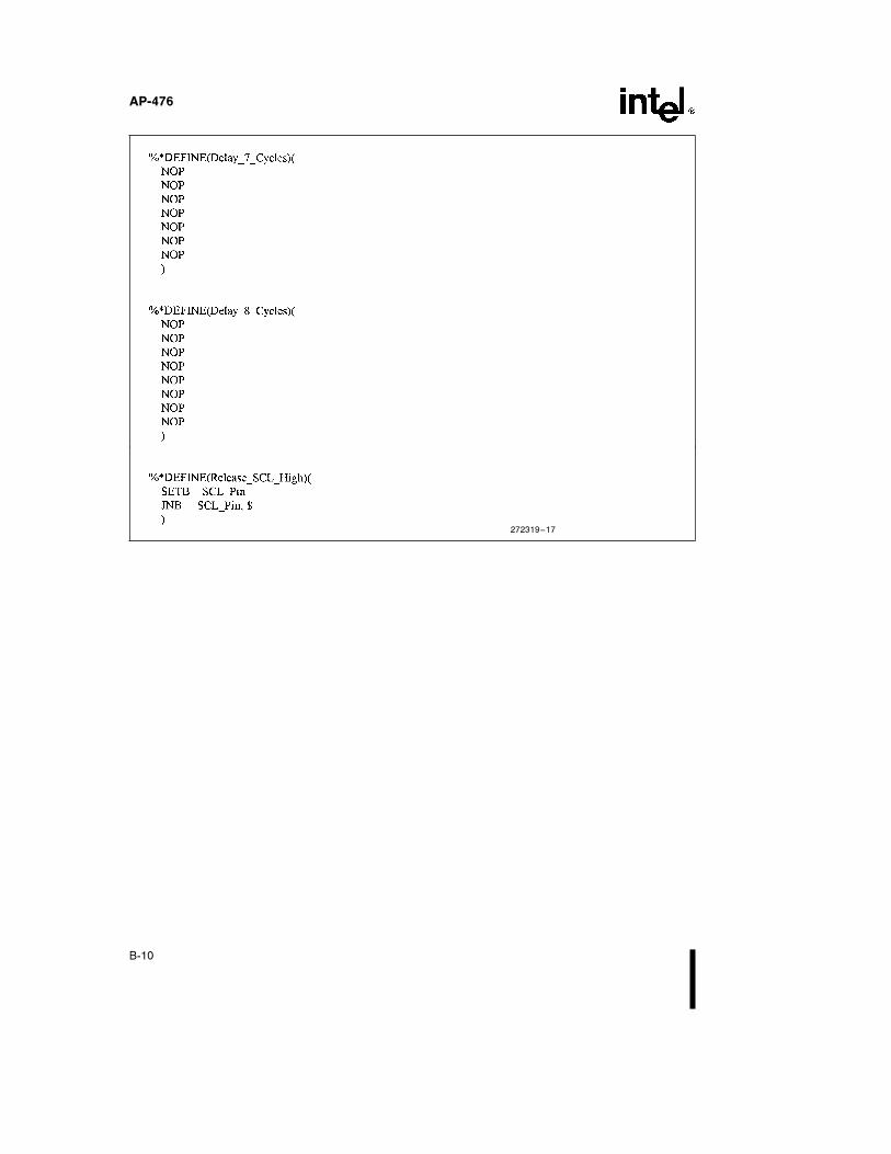
These ASM51 modules are listed at the end of the ap-plication note in Appendix A�
5
AP-476
MCS-51 and I2C-Bus Compatible IC’sSystem Implementation
This section of the application note explains the Mas-ter�Slave system diagrammed in Figure 1� The IntelMCS-51 is the Master Controller communicating withtwo I2C Slave peripherals� the PCF8570 RAM chipand SAAI064 LED driver� Information related to com-municating with these specific Slave devices can befound in the 1992 Philips I2C Peripherals for Micro-controllers Handbook�
The MCS-51 I2C Software Emulation Modules locatedin Appendix A are designed to demonstrate MasterController functionality�
As described above� the Intel 51 Master Controllertransmits data to the RAM device� receives it back andre-transmits it to the LED Slave driver� By using theSEND�MSG and RECV�MSG subroutines� bothMaster Transmit and Master Receive functionalitiesare demonstrated� Slave addresses used in these trans-fers are predefined values assigned by their manufactur-er� These values can be found in their respective data-books�
An I2C Master Transmission consists of the followingsteps�
1� Master polls the bus to see if free state exists
2� Master generates a START condition on the bus
3� Master broadcasts the Slave Address expecting anAcknowledge from the addressed Slave
4� Master transmits data bytes expecting acknowl-edgment status following each byte
5� Master generates a STOP condition and releasesthe bus
An I2C Master�Receive transaction consists of the ex-act same steps stated above EXCEPT�
4� Master receives data bytes sending an ACK to theSlave Transmitter after receipt of each byte� TheMaster signals receipt of the last data byte by re-sponding with the NOT Acknowledge condition�
MASTER TRANSMIT�RECEIVE
Bus transmission and evaluation is achieved by a nestedloop structure� SEND�DATA represents the outerloop which directs data transfers� TheMASTER�CONTROLLER subroutine polls the busto determine if any transactions are in progress� Errorchecking is performed at this level by evaluating thefollowing status flags� BUS�FAULT andI2C�BUSY� Based upon this information� the Masterwill either abort the transmit procedure or attempt tosend information� If bus control is granted as indicated
by cleared flags� the Master sends a START conditionand the Slave address� On the other hand� if either flagis set� the transmit procedure is aborted�
SEND�BYTE� the inner control loop� is responsiblefor transmitting 8 bits of each byte as well as monitor-ing Slave acknowledgment status� Each bit transferfrom I2C-bus lines checks for possible serial wait states�Wait states occur when slower devices need to commu-nicate on the bus with faster devices� Due to the wired-AND bus function� a Receiver can hold the clock lineSCL LOW forcing the Transmitter into this state� Datatransfer may continue when the Receiver is ready foranother byte of data as indicated by releasing the clockline SCL HIGH�
As stated in its section above� acknowledgment is re-quired to continue sending data bytes across the bus�However� situations may arise when a Receiver can notreceive another byte of data until it has performed someother function like servicing internal interrupts� If theSlave Receiver does not respond to a Master Transmit-ter data byte� not acknowledge could indicate that it isperforming some real-time function that prevents itfrom responding to I2C-bus communications� This situ-ation shows the flexibility and versatility of the bus�
The Master Receive process also utilizes the MAS-TER�CONTROLLER subroutine to gain control ofthe bus� When accepting data from the addressed Slave�in this case� RECV�DATA is the outer control loop�RECV�BYTE� the inner control loop� is responsiblefor receiving 8 bits of each byte as well as generatingthe Master’s acknowledgment condition� Similar totransmission� successful receipt of each byte is con-firmed by driving SDA LOW so that it remains stableLOW during the HIGH period of the SCL ACK pulse�Therefore� the Master still drives both SCL and SDAlines since control of the system clock is its responsibili-ty�
In both types of communication� Transmit�Receive�temporary RAM registers� BIT�CNT� BYTE�CNT�SLV�ADDR� and storage buffers� XMT�DAT�RCV�DAT� ALT�XMT� are integral parts of mostsubroutines because they are used for implementing theI2C protocol� Proper delays are implemented using theDELAY�X�CYCLES (X e any integer) macros�They give the designer flexibility to devise time delaysof any required length to satisfy system requirements�For example� to achieve the maximum bus speeds de-scribed in the next section� Delay�X�Cycle macroswere adjusted�
Lastly� the TRANSFER subroutine is provided to al-low predefined communication data programmed inthe microcontrollers EPROM to be transferred intoRegister RAM internal to the 51 device� It achieves this
6

AP-476
when used in conjunction with the SEND�MSG andRECV�MSG subroutines� However� when utilizingTRANSFER� the designer must conform their designto existing device Register RAM availability and to thefollowing message format�
Slave Address� � of Bytes to be Transmitted�Received� DataBytes (For Transmit Only)
The ASM-51 program demonstrating a complete Mas-ter Controller system is listed at the end of the applica-tion note in Appendix B� It writes the numeric datathat represents the following display ‘‘�I2C’’ to an I2Ccompatible IC (PCF8570 RAM)� reads the values backinto a buffer and transmits this buffer out to the PhilipsI2C SAA1064 LED driver to display the sequence�
I2C Software Emulation Performance
As demonstrated above� the Intel MCS-51 product linecan successfully implement the I2C Master Controllerfunctionality while maintaining data integrity and reli-able performance� The system outlined in Figure 1 wasevaluated for maximum bus performance and adher-ence to all I2C-bus specifications� Performance charac-terization was conducted at various crystal speeds onall devices listed in the MCS-51 Hardware Require-ments section of this application note�
When designing I2C software emulation systems� keepin mind that the designer has the flexibility to imple-ment large frequency ranges up to the I2C-bus maxi-mum� However� by making software changes to adjustbus frequencies� the newly modified program may nolonger meet required specifications and desired reliabil-ity standards� Therefore� designers should first alwaystake into consideration the bus performance level theywant to reach� After deciding this� an appropriate crys-tal can be chosen to achieve that implementation speed�The table below gives a few examples of system per-formance for two of the MCS-51 devices�
MCS-51 CrystalI2C Bus
Devices SpeedMaximum
Performance
8751BH 12 MHz 66�7 kHz
87C51 (FX-Core) 24 MHz 80�0 kHz
CONCLUSION
As a result of this evaluation� Intel MCS-51 microcon-trollers can be successfully interfaced to an I2C-bus sys-tem as a Master controller� The interface communicatesby ASM51 software emulation modules that have beentested on a wide array of I2C devices ranging from seri-al RAMS� Displays and a DTMF generators� No com-patibility problems have been seen to date� Therefore�when considering the implementation of your next I2C-bus Master Controller serial communication system�you have the option of using the Intel MCS-51 ProductLine�
REFERENCES
I2CBITS�ASM� G� Goodhue� Philips Semiconductors�August 1992�
The I2C-Bus and How to Use It (Including Specifica-tion)� Philips Semiconductors� January 1992�
I2C Peripherals for Microcontrollers� Philips Semicon-ductors� 1992 Data Handbook�
OM1016 I2C Evaluation Board� E� Rodgers and G�Moss� Philips Components Applications Lab Auck-land� New Zealand�
Programming the I2C Interface� Mitchell Kahn� SeniorEngineer� Intel Corporation�
7


AP-476
APPENDIX A
272319–1
A-1

AP-476
272319–2
A-2

AP-476
272319–3
A-3

AP-476
272319–4
A-4

AP-476
272319–5
A-5

AP-476
272319–6
A-6

AP-476
272319–7
A-7

AP-476
272319–24
A-8
AP-476
APPENDIX B
272319–8
B-1
AP-476
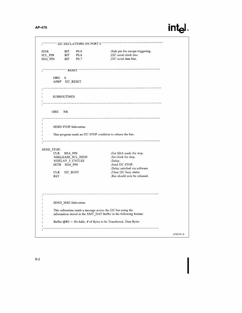
272319–9
B-2

AP-476
272319–10
B-3

AP-476
272319–11
B-4
AP-476
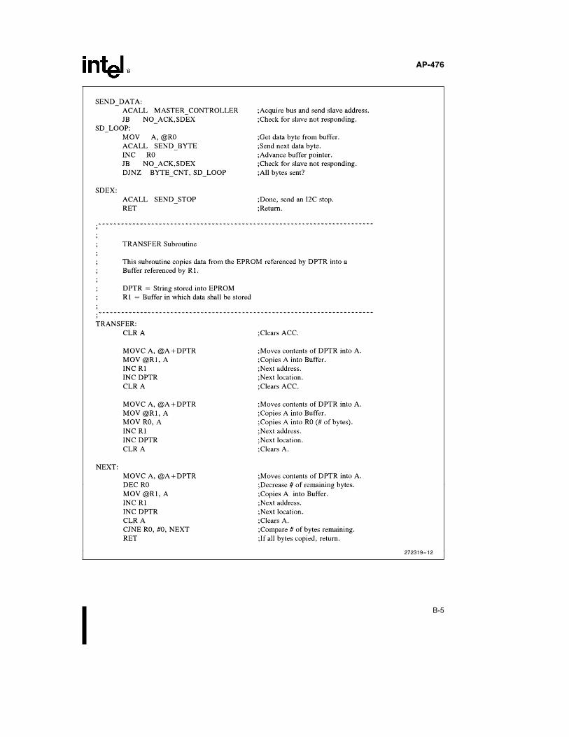
272319–12
B-5

AP-476
272319–13
B-6
AP-476
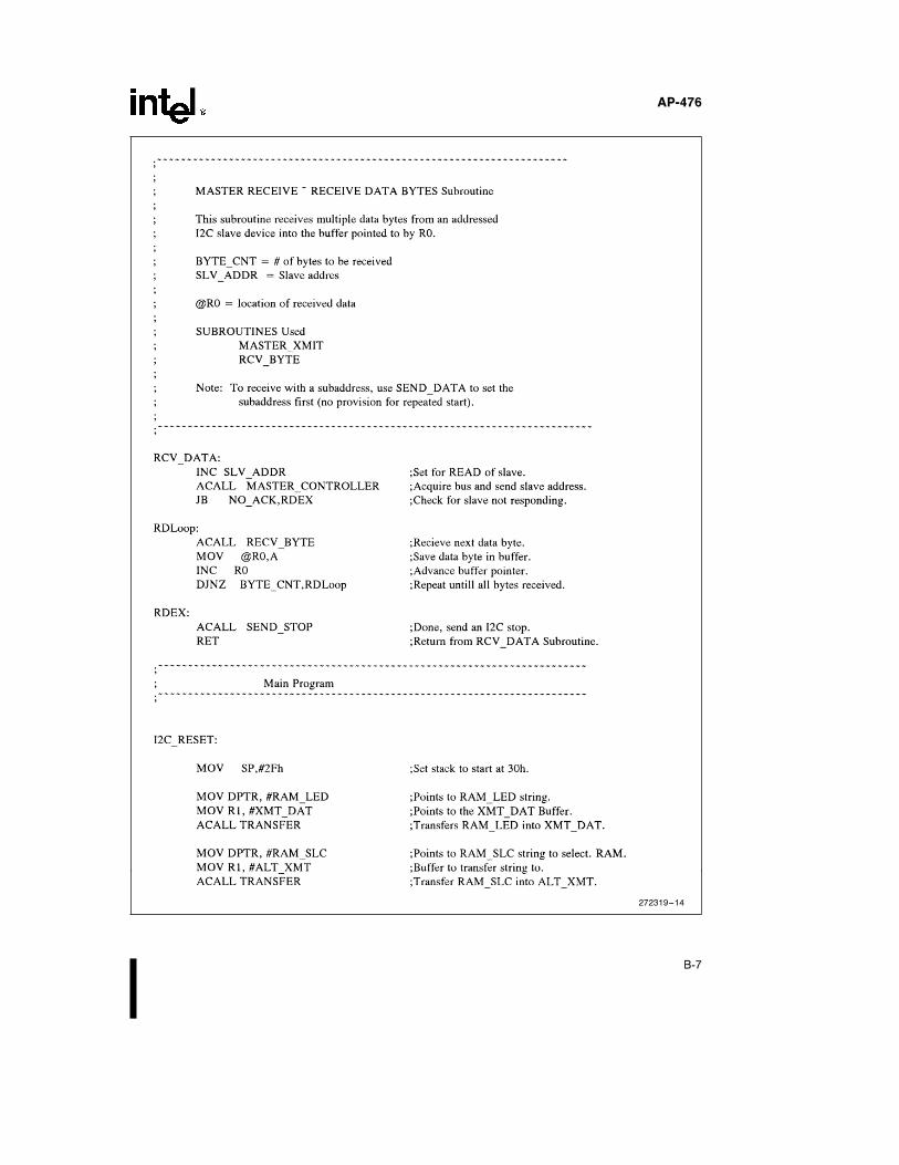
272319–14
B-7

AP-476
272319–15
B-8
AP-476
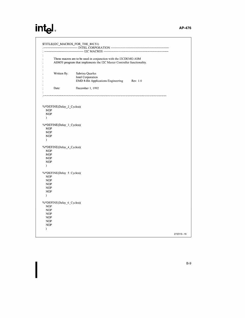
272319–16
B-9
AP-476
272319–17
B-10