HMC454ST89 454ST89E - Analog Devices · ideal driver amplifi er for Cellular/PCS/3G, WLL, ISM and...
12
For price, delivery and to place orders: Hittite Microwave Corporation, 20 Alpha Road, Chelmsford, MA 01824 Phone: 978-250-3343 Fax: 978-250-3373 Order On-line at www.hittite.com Application Support: Phone: 978-250-3343 or [email protected] 9 9 - 190 AMPLIFIERS - LINEAR & POWER - SMT HMC454ST89 / 454ST89E InGaP HBT ½ WATT HIGH IP3 AMPLIFIER, 0.4 - 2.5 GHz v05.0710 General Description Features Functional Diagram The HMC454ST89 & HMC454ST89E are high dynamic range GaAs InGaP Heterojunction Bipolar Transistor (HBT) ½ watt MMIC amplifiers operating between 0.4 and 2.5 GHz. Packaged in a low cost industry standard SOT89, the amplifier gain is typically 17.8 dB from 0.8 to 1.0 GHz and 12.5 dB from 1.8 to 2.2 GHz. Utilizing a minimum number of external components and a single +5V supply, the amplifier output IP3 can be optimized to +40 dBm at 0.9 GHz or +42 dBm at 2.0 GHz. The high output IP3 and PAE makes the HMC454ST89 an ideal driver amplifier for Cellular/PCS/3G, WLL, ISM and Fixed Wireless applications. Output IP3: +40 to +42 dBm Gain: 12.5 dB @ 2150 MHz 50% PAE @ +28 dBm Pout +17.5 dBm W-CDMA Channel Power@ -45 dBc ACP Single +5V Supply Industry Standard SOT89 Package Included in the HMC-DK002 Designer’s Kit Electrical Specifications, T A = +25°C, Vs= +5V [1] Typical Applications The HMC454ST89 / HMC454ST89E is ideal for applications requiring a high dynamic range amplifier: • GSM, GPRS & EDGE • CDMA & W-CDMA • CATV/Cable Modem • Fixed Wireless & WLL Parameter Min. Typ. Max. Min. Typ. Max. Min. Typ. Max. Units Frequency Range 824 - 960 1800 - 2000 2000 - 2200 MHz Gain 16 17.8 11 12.5 11 12.5 dB Gain Variation Over Temperature 0.008 0.016 0.008 0.016 0.008 0.016 dB / °C Input Return Loss 9 7 12 dB Output Return Loss 13 21 19 dB Output Power for 1dB Compression (P1dB) 22 24.5 24 27 24 27.5 dBm Saturated Output Power (Psat) 25.5 28.5 28.5 dBm Output Third Order Intercept (IP3) [2] 37 40 38 41 38 42 dBm Noise Figure 8 6.5 5.2 dB Supply Current (Icq) 150 175 150 175 150 175 mA [1] Specifications and data reflect HMC454ST89 measured using the respective application circuits for each designated frequency band found herein. Contact the HMC Applications Group for assistance in optimizing performance for your application. [2] Two-tone input power of 0 dBm per tone, 1 MHz spacing. Information furnished by Analog Devices is believed to be accurate and reliable. However, no responsibility is assumed by Analog Devices for its use, nor for any infringements of patents or other rights of third parties that may result from its use. Specifications subject to change without notice. No license is granted by implication or otherwise under any patent or patent rights of Analog Devices. Trademarks and registered trademarks are the property of their respective owners. For price, delivery, and to place orders: Analog Devices, Inc., One Technology Way, P.O. Box 9106, Norwood, MA 02062-9106 Phone: 781-329-4700 • Order online at www.analog.com Application Support: Phone: 1-800-ANALOG-D
Transcript of HMC454ST89 454ST89E - Analog Devices · ideal driver amplifi er for Cellular/PCS/3G, WLL, ISM and...

For price, delivery and to place orders: Hittite Microwave Corporation, 20 Alpha Road, Chelmsford, MA 01824Phone: 978-250-3343 Fax: 978-250-3373 Order On-line at www.hittite.com
Application Support: Phone: 978-250-3343 or [email protected]
9
9 - 190
AM
PLI
FIE
RS
- L
INE
AR
& P
OW
ER
- S
MT
HMC454ST89 / 454ST89E
InGaP HBT ½ WATT HIGH IP3
AMPLIFIER, 0.4 - 2.5 GHz
v05.0710
General Description
Features
Functional Diagram
The HMC454ST89 & HMC454ST89E are high dynamic range GaAs InGaP Heterojunction Bipolar Transistor (HBT) ½ watt MMIC amplifi ers operating between 0.4 and 2.5 GHz. Packaged in a low cost industry standard SOT89, the amplifi er gain is typically 17.8 dB from 0.8 to 1.0 GHz and 12.5 dB from 1.8 to 2.2 GHz. Utilizing a minimum number of external components and a single +5V supply, the amplifi er output IP3 can be optimized to +40 dBm at 0.9 GHz or +42 dBm at 2.0 GHz. The high output IP3 and PAE makes the HMC454ST89 an ideal driver amplifi er for Cellular/PCS/3G, WLL, ISM and Fixed Wireless applications.
Output IP3: +40 to +42 dBm
Gain: 12.5 dB @ 2150 MHz
50% PAE @ +28 dBm Pout
+17.5 dBm W-CDMA Channel Power@ -45 dBc ACP
Single +5V Supply
Industry Standard SOT89 Package
Included in the HMC-DK002 Designer’s Kit
Electrical Specifi cations, TA = +25°C, Vs= +5V [1]
Typical Applications
The HMC454ST89 / HMC454ST89E is ideal for applications requiring a high dynamic range amplifi er:
• GSM, GPRS & EDGE
• CDMA & W-CDMA
• CATV/Cable Modem
• Fixed Wireless & WLL
Parameter Min. Typ. Max. Min. Typ. Max. Min. Typ. Max. Units
Frequency Range 824 - 960 1800 - 2000 2000 - 2200 MHz
Gain 16 17.8 11 12.5 11 12.5 dB
Gain Variation Over Temperature 0.008 0.016 0.008 0.016 0.008 0.016 dB / °C
Input Return Loss 9 7 12 dB
Output Return Loss 13 21 19 dB
Output Power for 1dB Compression (P1dB) 22 24.5 24 27 24 27.5 dBm
Saturated Output Power (Psat) 25.5 28.5 28.5 dBm
Output Third Order Intercept (IP3) [2] 37 40 38 41 38 42 dBm
Noise Figure 8 6.5 5.2 dB
Supply Current (Icq) 150 175 150 175 150 175 mA
[1] Specifi cations and data refl ect HMC454ST89 measured using the respective application circuits for each designated frequency band found herein. Contact the HMC Applications Group for assistance in optimizing performance for your application.[2] Two-tone input power of 0 dBm per tone, 1 MHz spacing.
Information furnished by Analog Devices is believed to be accurate and reliable. However, no responsibility is assumed by Analog Devices for its use, nor for any infringements of patents or other rights of third parties that may result from its use. Specifications subject to change without notice. No license is granted by implication or otherwise under any patent or patent rights of Analog Devices. Trademarks and registered trademarks are the property of their respective owners.
For price, delivery, and to place orders: Analog Devices, Inc., One Technology Way, P.O. Box 9106, Norwood, MA 02062-9106 Phone: 781-329-4700 • Order online at www.analog.com Application Support: Phone: 1-800-ANALOG-D

For price, delivery and to place orders: Hittite Microwave Corporation, 20 Alpha Road, Chelmsford, MA 01824Phone: 978-250-3343 Fax: 978-250-3373 Order On-line at www.hittite.com
Application Support: Phone: 978-250-3343 or [email protected]
AM
PLI
FIE
RS
- L
INE
AR
& P
OW
ER
- S
MT
9
9 - 191
Input Return Loss
vs. Temperature @ 900 MHz
Output Return Loss
vs. Temperature @ 900 MHz
Broadband Gain
& Return Loss @ 900 MHz Gain vs. Temperature @ 900 MHz
P1dB vs. Temperature @ 900 MHz Psat vs. Temperature @ 900 MHz
-20
-15
-10
-5
0
5
10
15
20
25
0.4 0.5 0.6 0.7 0.8 0.9 1 1.1 1.2 1.3 1.4
S21S11S22
RE
SP
ON
SE
(dB
)
FREQUENCY (GHz)
10
11
12
13
14
15
16
17
18
19
20
0.7 0.8 0.9 1 1.1 1.2
+25 C+85 C -40 C
GA
IN (
dB)
FREQUENCY (GHz)
-25
-20
-15
-10
-5
0
0.7 0.8 0.9 1 1.1 1.2
+25 C+85 C -40 C
RE
TU
RN
LO
SS
(dB
)
FREQUENCY (GHz)
-20
-15
-10
-5
0
0.7 0.8 0.9 1 1.1 1.2
+25 C+85 C -40 C
RE
TU
RN
LO
SS
(dB
)
FREQUENCY (GHz)
20
21
22
23
24
25
26
27
28
29
30
0.7 0.8 0.9 1 1.1 1.2
+25 C+85 C -40 C
P1d
B (
dBm
)
FREQUENCY (GHz)
20
21
22
23
24
25
26
27
28
29
30
0.7 0.8 0.9 1 1.1 1.2
+25 C+85 C -40 C
PS
AT
(dB
m)
FREQUENCY (GHz)
HMC454ST89 / 454ST89Ev05.0710
InGaP HBT ½ WATT HIGH IP3
AMPLIFIER, 0.4 - 2.5 GHz
Information furnished by Analog Devices is believed to be accurate and reliable. However, no responsibility is assumed by Analog Devices for its use, nor for any infringements of patents or other rights of third parties that may result from its use. Specifications subject to change without notice. No license is granted by implication or otherwise under any patent or patent rights of Analog Devices. Trademarks and registered trademarks are the property of their respective owners.
For price, delivery, and to place orders: Analog Devices, Inc., One Technology Way, P.O. Box 9106, Norwood, MA 02062-9106 Phone: 781-329-4700 • Order online at www.analog.com Application Support: Phone: 1-800-ANALOG-D

For price, delivery and to place orders: Hittite Microwave Corporation, 20 Alpha Road, Chelmsford, MA 01824Phone: 978-250-3343 Fax: 978-250-3373 Order On-line at www.hittite.com
Application Support: Phone: 978-250-3343 or [email protected]
9
9 - 192
AM
PLI
FIE
RS
- L
INE
AR
& P
OW
ER
- S
MT
Output IP3 vs. Temperature @ 900 MHz Noise Figure vs. Temperature @ 900 MHz
Gain, Power & Output IP3
vs. Supply Voltage @ 900 MHz
Reverse Isolation
vs. Temperature @ 900 MHz
34
35
36
37
38
39
40
41
42
43
44
0.7 0.8 0.9 1 1.1 1.2
+25 C+85 C -40 C
IP3
(dB
m)
FREQUENCY (GHz)
5
6
7
8
9
10
11
12
13
14
15
0.7 0.8 0.9 1 1.1 1.2
+25 C+85 C -40 C
NO
ISE
FIG
UR
E (
dB)
FREQUENCY (GHz)
-40
-35
-30
-25
-20
-15
-10
-5
0
0.7 0.8 0.9 1 1.1 1.2
+25 C+85 C -40 C
ISO
LAT
ION
(dB
)
FREQUENCY (GHz)
5
10
15
20
25
30
35
40
45
4.5 4.75 5 5.25 5.5
GAINP1dB
PSATIP3
GA
IN (
dB),
P1d
B (
dBm
), P
SA
T (
dBm
), IP
3 (d
Bm
)
Vs (V)
5.5V
5.0V
4.5V
-80
-75
-70
-65
-60
-55
-50
-45
-40
-35
-30
7 8 9 10 11 12 13 14 15 16 17 18 19
AC
PR
(dB
c)
Channel Output Power (dBm)
CDMA IS95Frequency : 880 MHzIntegration BW: 1.228 MHz Forward Link, 9 Channels
Source ACPR
ACPR vs. Supply Voltage @ 880 MHz
CDMA IS95, 9 Channels Forward
HMC454ST89 / 454ST89Ev05.0710
InGaP HBT ½ WATT HIGH IP3
AMPLIFIER, 0.4 - 2.5 GHz
Information furnished by Analog Devices is believed to be accurate and reliable. However, no responsibility is assumed by Analog Devices for its use, nor for any infringements of patents or other rights of third parties that may result from its use. Specifications subject to change without notice. No license is granted by implication or otherwise under any patent or patent rights of Analog Devices. Trademarks and registered trademarks are the property of their respective owners.
For price, delivery, and to place orders: Analog Devices, Inc., One Technology Way, P.O. Box 9106, Norwood, MA 02062-9106 Phone: 781-329-4700 • Order online at www.analog.com Application Support: Phone: 1-800-ANALOG-D

For price, delivery and to place orders: Hittite Microwave Corporation, 20 Alpha Road, Chelmsford, MA 01824Phone: 978-250-3343 Fax: 978-250-3373 Order On-line at www.hittite.com
Application Support: Phone: 978-250-3343 or [email protected]
AM
PLI
FIE
RS
- L
INE
AR
& P
OW
ER
- S
MT
9
9 - 193
Input Return Loss
vs. Temperature @ 1960 MHz
Output Return Loss
vs. Temperature @ 1960 MHz
Broadband Gain
& Return Loss @ 1960 MHz Gain vs. Temperature @ 1960 MHz
P1dB vs. Temperature @ 1960 MHz Psat vs. Temperature @ 1960 MHz
-25
-20
-15
-10
-5
0
5
10
15
20
25
1 1.2 1.4 1.6 1.8 2 2.2 2.4 2.6 2.8 3
S21S11S22
RE
SP
ON
SE
(dB
)
FREQUENCY (GHz)
5
6
7
8
9
10
11
12
13
14
15
1.7 1.8 1.9 2 2.1 2.2
+25 C+85 C -40 C
GA
IN (
dB)
FREQUENCY (GHz)
-20
-15
-10
-5
0
1.7 1.8 1.9 2 2.1 2.2
+25 C+85 C -40 C
RE
TU
RN
LO
SS
(dB
)
FREQUENCY (GHz)
-25
-20
-15
-10
-5
0
1.7 1.8 1.9 2 2.1 2.2
+25 C+85 C -40 C
RE
TU
RN
LO
SS
(dB
)
FREQUENCY (GHz)
22
23
24
25
26
27
28
29
30
31
32
1.7 1.8 1.9 2 2.1 2.2
+25 C+85 C -40 C
P1d
B (
dBm
)
FREQUENCY (GHz)
22
23
24
25
26
27
28
29
30
31
32
1.7 1.8 1.9 2 2.1 2.2
+25 C+85 C -40 C
PS
AT
(dB
m)
FREQUENCY (GHz)
HMC454ST89 / 454ST89Ev05.0710
InGaP HBT ½ WATT HIGH IP3
AMPLIFIER, 0.4 - 2.5 GHz
Information furnished by Analog Devices is believed to be accurate and reliable. However, no responsibility is assumed by Analog Devices for its use, nor for any infringements of patents or other rights of third parties that may result from its use. Specifications subject to change without notice. No license is granted by implication or otherwise under any patent or patent rights of Analog Devices. Trademarks and registered trademarks are the property of their respective owners.
For price, delivery, and to place orders: Analog Devices, Inc., One Technology Way, P.O. Box 9106, Norwood, MA 02062-9106 Phone: 781-329-4700 • Order online at www.analog.com Application Support: Phone: 1-800-ANALOG-D

For price, delivery and to place orders: Hittite Microwave Corporation, 20 Alpha Road, Chelmsford, MA 01824Phone: 978-250-3343 Fax: 978-250-3373 Order On-line at www.hittite.com
Application Support: Phone: 978-250-3343 or [email protected]
9
9 - 194
AM
PLI
FIE
RS
- L
INE
AR
& P
OW
ER
- S
MT
Output IP3 vs. Temperature @ 1960 MHzNoise Figure
vs. Temperature @ 1960 MHz
Gain, Power & Output IP3
vs. Supply Voltage @ 1960 MHz
Reverse Isolation
vs. Temperature @ 1960 MHz
34
35
36
37
38
39
40
41
42
43
44
1.7 1.8 1.9 2 2.1 2.2
+25 C+85 C -40 C
IP3
(dB
m)
FREQUENCY (GHz)
0
1
2
3
4
5
6
7
8
9
10
1.7 1.8 1.9 2 2.1 2.2
+25 C+85 C -40 CN
OIS
E F
IGU
RE
(dB
)
FREQUENCY (GHz)
-25
-20
-15
-10
-5
0
1.7 1.8 1.9 2 2.1 2.2
+25 C+85 C -40 C
ISO
LAT
ION
(dB
)
FREQUENCY (GHz)
5
10
15
20
25
30
35
40
45
4.5 4.75 5 5.25 5.5
GAINP1dB
PSATIP3
GA
IN (
dB),
P1d
B (
dBm
), P
SA
T (
dBm
), IP
3 (d
Bm
)
Vs (V)
ACPR vs. Supply Voltage @ 1.96 GHz
CDMA 2000, 9 Channels Forward
ACPR vs. Supply Voltage @ 2.14 GHz
W-CDMA, 64 DPCH
4.5V
-70
-65
-60
-55
-50
-45
-40
-35
-30
0 2 4 6 8 10 12 14 16 18 20
AC
PR
(dB
c)
Channel Output Power (dBm)
WCDMAFrequency : 2.14 GHzIntegration BW: 3.84 MHz64 DPCH
5.5V
Source ACPR
5.0V
5.5V
5.0V
4.5V
-85
-80
-75
-70
-65
-60
-55
-50
-45
-40
2 4 6 8 10 12 14 16 18 20 22
AC
PR
(dB
c)
Channel Output Power (dBm)
CDMA2000 Rev. 8Frequency : 1.96 GHzIntegration BW: 1.228 MHzForward Link, SRI, 9 CHANNELS
Source ACPR
HMC454ST89 / 454ST89Ev05.0710
InGaP HBT ½ WATT HIGH IP3
AMPLIFIER, 0.4 - 2.5 GHz
Information furnished by Analog Devices is believed to be accurate and reliable. However, no responsibility is assumed by Analog Devices for its use, nor for any infringements of patents or other rights of third parties that may result from its use. Specifications subject to change without notice. No license is granted by implication or otherwise under any patent or patent rights of Analog Devices. Trademarks and registered trademarks are the property of their respective owners.
For price, delivery, and to place orders: Analog Devices, Inc., One Technology Way, P.O. Box 9106, Norwood, MA 02062-9106 Phone: 781-329-4700 • Order online at www.analog.com Application Support: Phone: 1-800-ANALOG-D
For price, delivery and to place orders: Hittite Microwave Corporation, 20 Alpha Road, Chelmsford, MA 01824Phone: 978-250-3343 Fax: 978-250-3373 Order On-line at www.hittite.com
Application Support: Phone: 978-250-3343 or [email protected]
AM
PLI
FIE
RS
- L
INE
AR
& P
OW
ER
- S
MT
9
9 - 195
Outline Drawing
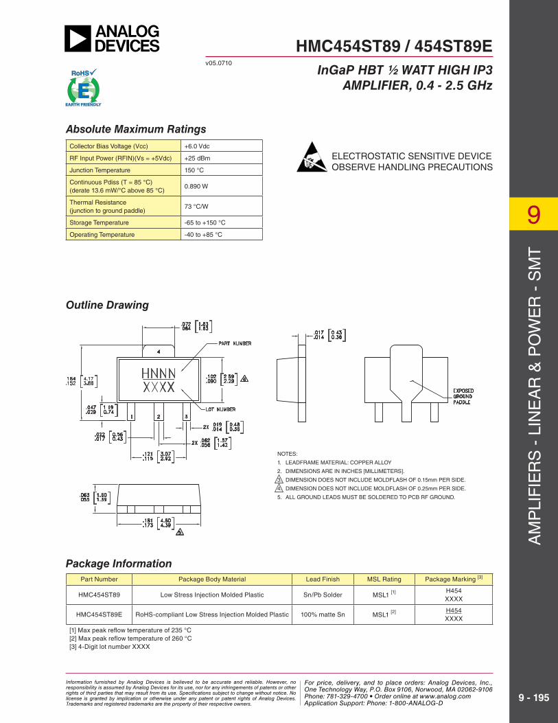
Absolute Maximum Ratings
Collector Bias Voltage (Vcc) +6.0 Vdc
RF Input Power (RFIN)(Vs = +5Vdc) +25 dBm
Junction Temperature 150 °C
Continuous Pdiss (T = 85 °C)(derate 13.6 mW/°C above 85 °C)
0.890 W
Thermal Resistance(junction to ground paddle)
73 °C/W
Storage Temperature -65 to +150 °C
Operating Temperature -40 to +85 °C
Part Number Package Body Material Lead Finish MSL Rating Package Marking [3]
HMC454ST89 Low Stress Injection Molded Plastic Sn/Pb Solder MSL1 [1] H454XXXX
HMC454ST89E RoHS-compliant Low Stress Injection Molded Plastic 100% matte Sn MSL1 [2] H454XXXX
[1] Max peak refl ow temperature of 235 °C[2] Max peak refl ow temperature of 260 °C[3] 4-Digit lot number XXXX
Package Information
NOTES:
1. LEADFRAME MATERIAL: COPPER ALLOY
2. DIMENSIONS ARE IN INCHES [MILLIMETERS].
3. DIMENSION DOES NOT INCLUDE MOLDFLASH OF 0.15mm PER SIDE.
4. DIMENSION DOES NOT INCLUDE MOLDFLASH OF 0.25mm PER SIDE.
5. ALL GROUND LEADS MUST BE SOLDERED TO PCB RF GROUND.
ELECTROSTATIC SENSITIVE DEVICEOBSERVE HANDLING PRECAUTIONS
HMC454ST89 / 454ST89Ev05.0710
InGaP HBT ½ WATT HIGH IP3
AMPLIFIER, 0.4 - 2.5 GHz
Information furnished by Analog Devices is believed to be accurate and reliable. However, no responsibility is assumed by Analog Devices for its use, nor for any infringements of patents or other rights of third parties that may result from its use. Specifications subject to change without notice. No license is granted by implication or otherwise under any patent or patent rights of Analog Devices. Trademarks and registered trademarks are the property of their respective owners.
For price, delivery, and to place orders: Analog Devices, Inc., One Technology Way, P.O. Box 9106, Norwood, MA 02062-9106 Phone: 781-329-4700 • Order online at www.analog.com Application Support: Phone: 1-800-ANALOG-D

For price, delivery and to place orders: Hittite Microwave Corporation, 20 Alpha Road, Chelmsford, MA 01824Phone: 978-250-3343 Fax: 978-250-3373 Order On-line at www.hittite.com
Application Support: Phone: 978-250-3343 or [email protected]
9
9 - 196
AM
PLI
FIE
RS
- L
INE
AR
& P
OW
ER
- S
MT
900 MHz Application Circuit, Compact Layout
Recommended Component Values
L1, L2 1 nH
L3 36 nH
R1 5.1 Ohms
C1 8 pF
C2 22 pF
C3 2.7 pF
C4, C6 100 pF
C5 2.2 μF
TL1
Impedance 50 Ohm
Physical Length 0.050”
Electrical Length 2.5°
PCB Material: 10 mil Rogers 4350, Er = 3.48
This circuit was used to specify the performance for 894-960 MHz operation. This circuit will satisfy many applications from 700 to 1200 MHz. Contact the HMC Applications Group for assistance in optimizing performance for your application.
Pin Descriptions
Pin Number Function Description Interface Schematic
1 RFINThis pin is AC coupled.
Off chip matching components are required. See Application Circuit herein.
3 RFOUTRF output and DC Bias input for the output amplifi er stage.
Off chip matching components are required. See Application Circuit herein.
2,4 GNDThese pins & package bottom must be connected to
RF/DC ground.
HMC454ST89 / 454ST89Ev05.0710
InGaP HBT ½ WATT HIGH IP3
AMPLIFIER, 0.4 - 2.5 GHz
Information furnished by Analog Devices is believed to be accurate and reliable. However, no responsibility is assumed by Analog Devices for its use, nor for any infringements of patents or other rights of third parties that may result from its use. Specifications subject to change without notice. No license is granted by implication or otherwise under any patent or patent rights of Analog Devices. Trademarks and registered trademarks are the property of their respective owners.
For price, delivery, and to place orders: Analog Devices, Inc., One Technology Way, P.O. Box 9106, Norwood, MA 02062-9106 Phone: 781-329-4700 • Order online at www.analog.com Application Support: Phone: 1-800-ANALOG-D

For price, delivery and to place orders: Hittite Microwave Corporation, 20 Alpha Road, Chelmsford, MA 01824Phone: 978-250-3343 Fax: 978-250-3373 Order On-line at www.hittite.com
Application Support: Phone: 978-250-3343 or [email protected]
AM
PLI
FIE
RS
- L
INE
AR
& P
OW
ER
- S
MT
9
9 - 197
900 MHz Evaluation PCB
The circuit board used in this application should use RF circuit design techniques. Signal lines should have 50 Ohm impedance while the package ground leads and exposed paddle should be connected directly to the ground plane similar to that shown. A sufficient number of via holes should be used to connect the top and bottom ground planes. The evaluation board should be mounted to an appro-priate heat sink. The evaluation circuit board shown is available from Hittite upon request.
List of Materials for Evaluation PCB 107755 [1]
Item Description
J1 - J2 PCB Mount SMA Connector
J3 -J4 DC Pins
C1 8 pF Capacitor, 0402 Pkg.
C2 22 pF Capacitor, 0402 Pkg.
C3 2.7 pF Capacitor, 0402 Pkg.
C4, C6 100 pF Capacitor, 0402 Pkg.
C5 2.2 μF Capacitor, Tantalum
L1, L2 1 nH Inductor, 0402 Pkg.
L3 36 nH Inductor, 0402 Pkg.
R1 5.1 Ohms
U1HMC454ST89 / HMC454ST89ELinear Amp
PCB [2] 107753 Evaluation PCB, 10 mils
[1] Reference this number when ordering complete evaluation PCB
[2] Circuit Board Material: Rogers 4350, Er = 3.48
HMC454ST89 / 454ST89Ev05.0710
InGaP HBT ½ WATT HIGH IP3
AMPLIFIER, 0.4 - 2.5 GHz
Information furnished by Analog Devices is believed to be accurate and reliable. However, no responsibility is assumed by Analog Devices for its use, nor for any infringements of patents or other rights of third parties that may result from its use. Specifications subject to change without notice. No license is granted by implication or otherwise under any patent or patent rights of Analog Devices. Trademarks and registered trademarks are the property of their respective owners.
For price, delivery, and to place orders: Analog Devices, Inc., One Technology Way, P.O. Box 9106, Norwood, MA 02062-9106 Phone: 781-329-4700 • Order online at www.analog.com Application Support: Phone: 1-800-ANALOG-D

For price, delivery and to place orders: Hittite Microwave Corporation, 20 Alpha Road, Chelmsford, MA 01824Phone: 978-250-3343 Fax: 978-250-3373 Order On-line at www.hittite.com
Application Support: Phone: 978-250-3343 or [email protected]
9
9 - 198
AM
PLI
FIE
RS
- L
INE
AR
& P
OW
ER
- S
MT
1960 & 2140 MHz Application Circuit
Recommended Component Values
L1 8.2 nH
C1 1 pF
C2 1.2 pF
C3 3 pF
C4 100 pF
C5 2.2 μF
TL1 TL2 T3 TL4
Impedance 50 Ohm 50 Ohm 50 Ohm 50 Ohm
Physical Length 0.32” 0.10” 0.07” 0.17”
Electrical Length 34° 11° 8° 18.5°
PCB Material: 10 mil Rogers 4350, Er = 3.48
This circuit was used to specify the performance for 1800-2000 and 2000-2200 MHz operation. This circuit will satisfy many applications from 1700 to 2500 MHz. Contact the HMC Applications Group for assistance in optimizing performance for your application.
HMC454ST89 / 454ST89Ev05.0710
InGaP HBT ½ WATT HIGH IP3
AMPLIFIER, 0.4 - 2.5 GHz
Information furnished by Analog Devices is believed to be accurate and reliable. However, no responsibility is assumed by Analog Devices for its use, nor for any infringements of patents or other rights of third parties that may result from its use. Specifications subject to change without notice. No license is granted by implication or otherwise under any patent or patent rights of Analog Devices. Trademarks and registered trademarks are the property of their respective owners.
For price, delivery, and to place orders: Analog Devices, Inc., One Technology Way, P.O. Box 9106, Norwood, MA 02062-9106 Phone: 781-329-4700 • Order online at www.analog.com Application Support: Phone: 1-800-ANALOG-D

For price, delivery and to place orders: Hittite Microwave Corporation, 20 Alpha Road, Chelmsford, MA 01824Phone: 978-250-3343 Fax: 978-250-3373 Order On-line at www.hittite.com
Application Support: Phone: 978-250-3343 or [email protected]
AM
PLI
FIE
RS
- L
INE
AR
& P
OW
ER
- S
MT
9
9 - 199
1960 & 2140 MHz Evaluation PCB
The circuit board used in this application should use RF circuit design techniques. Signal lines should have 50 Ohm impedance while the package ground leads and exposed paddle should be connected directly to the ground plane similar to that shown. A sufficient number of via holes should be used to connect the top and bottom ground planes. The evaluation board should be mounted to an appro-priate heat sink. The evaluation circuit board shown is available from Hittite upon request.
List of Materials for Evaluation PCB 107749 [1]
Item Description
J1 - J2 PCB Mount SMA Connector
J3 - J4 DC Pins
C1 1.0 pF Capacitor, 0402 Pkg.
C2 1.2 pF Capacitor, 0402 Pkg.
C3 3.0 pF Capacitor, 0402 Pkg.
C4 100 pF Capacitor, 0402 Pkg.
C5 2.2 μF Capacitor, Tantalum
L1 8.2 nH Inductor, 0402 Pkg.
U1 HMC454ST89 / HMC454ST89E
PCB [2] 107747 Evaluation PCB, 10 mils
[1] Reference this number when ordering complete evaluation PCB
[2] Circuit Board Material: Rogers 4350, Er = 3.48
HMC454ST89 / 454ST89Ev05.0710
InGaP HBT ½ WATT HIGH IP3
AMPLIFIER, 0.4 - 2.5 GHz
Information furnished by Analog Devices is believed to be accurate and reliable. However, no responsibility is assumed by Analog Devices for its use, nor for any infringements of patents or other rights of third parties that may result from its use. Specifications subject to change without notice. No license is granted by implication or otherwise under any patent or patent rights of Analog Devices. Trademarks and registered trademarks are the property of their respective owners.
For price, delivery, and to place orders: Analog Devices, Inc., One Technology Way, P.O. Box 9106, Norwood, MA 02062-9106 Phone: 781-329-4700 • Order online at www.analog.com Application Support: Phone: 1-800-ANALOG-D

For price, delivery and to place orders: Hittite Microwave Corporation, 20 Alpha Road, Chelmsford, MA 01824Phone: 978-250-3343 Fax: 978-250-3373 Order On-line at www.hittite.com
Application Support: Phone: 978-250-3343 or [email protected]
9
9 - 200
AM
PLI
FIE
RS
- L
INE
AR
& P
OW
ER
- S
MT
Recommended Component Values
L1 18 nH
C1 4 pF
C2, C6 10 pF
C3 3 pF
C4 100 pF
C5 2.2 μF
TL1 TL2 TL3
Impedance 50 Ohm 50 Ohm 50 Ohm
Physical Length 0.35” 0.05” 0.53”
Electrical Length 18° 2.5° 27°
PCB Material: 10 mil Rogers 4350, Er = 3.48
Broadband Gain & Return Loss
-15
-10
-5
0
5
10
15
20
25
0.4 0.5 0.6 0.7 0.8 0.9 1 1.1 1.2 1.3 1.4
S21S11S22
RE
SP
ON
SE
(dB
)
FREQUENCY (GHz)
20
25
30
35
40
45
50
0.7 0.8 0.9 1 1.1 1.2
IP3P1dB
IP3
(dB
m),
P1d
B (
dBm
)
FREQUENCY (GHz)
Output IP3 & P1dB
Alternative 900 MHz Application Circuit, Optimal OIP3 Layout
This alternate application circuit for 900 MHz applications features a resonating I/O structure on the PCB that, while using more PCB area, will improve output IP3 from +40 dBm to +42 dBm. This circuit will satisfy many applications from 700 to 1200 MHz as the typical performance below demonstrates. Contact the HMC Applications Group for assistance in optimizing performance for your application.
HMC454ST89 / 454ST89Ev05.0710
InGaP HBT ½ WATT HIGH IP3
AMPLIFIER, 0.4 - 2.5 GHz
Information furnished by Analog Devices is believed to be accurate and reliable. However, no responsibility is assumed by Analog Devices for its use, nor for any infringements of patents or other rights of third parties that may result from its use. Specifications subject to change without notice. No license is granted by implication or otherwise under any patent or patent rights of Analog Devices. Trademarks and registered trademarks are the property of their respective owners.
For price, delivery, and to place orders: Analog Devices, Inc., One Technology Way, P.O. Box 9106, Norwood, MA 02062-9106 Phone: 781-329-4700 • Order online at www.analog.com Application Support: Phone: 1-800-ANALOG-D
For price, delivery and to place orders: Hittite Microwave Corporation, 20 Alpha Road, Chelmsford, MA 01824Phone: 978-250-3343 Fax: 978-250-3373 Order On-line at www.hittite.com
Application Support: Phone: 978-250-3343 or [email protected]
AM
PLI
FIE
RS
- L
INE
AR
& P
OW
ER
- S
MT
9
9 - 201
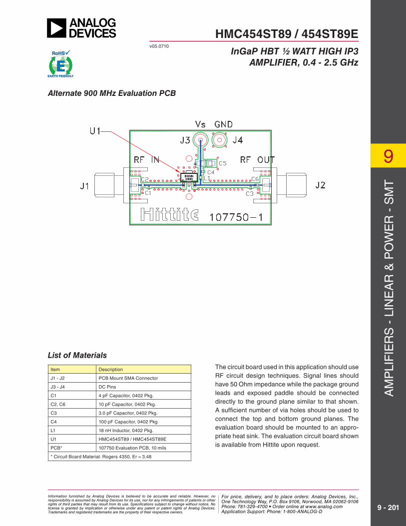
Alternate 900 MHz Evaluation PCB
The circuit board used in this application should use RF circuit design techniques. Signal lines should have 50 Ohm impedance while the package ground leads and exposed paddle should be connected directly to the ground plane similar to that shown. A sufficient number of via holes should be used to connect the top and bottom ground planes. The evaluation board should be mounted to an appro-priate heat sink. The evaluation circuit board shown is available from Hittite upon request.
List of Materials
Item Description
J1 - J2 PCB Mount SMA Connector
J3 - J4 DC Pins
C1 4 pF Capacitor, 0402 Pkg.
C2, C6 10 pF Capacitor, 0402 Pkg.
C3 3.0 pF Capacitor, 0402 Pkg.
C4 100 pF Capacitor, 0402 Pkg
L1 18 nH Inductor, 0402 Pkg.
U1 HMC454ST89 / HMC454ST89E
PCB* 107750 Evaluation PCB, 10 mils
* Circuit Board Material: Rogers 4350, Er = 3.48
HMC454ST89 / 454ST89Ev05.0710
InGaP HBT ½ WATT HIGH IP3
AMPLIFIER, 0.4 - 2.5 GHz
Information furnished by Analog Devices is believed to be accurate and reliable. However, no responsibility is assumed by Analog Devices for its use, nor for any infringements of patents or other rights of third parties that may result from its use. Specifications subject to change without notice. No license is granted by implication or otherwise under any patent or patent rights of Analog Devices. Trademarks and registered trademarks are the property of their respective owners.
For price, delivery, and to place orders: Analog Devices, Inc., One Technology Way, P.O. Box 9106, Norwood, MA 02062-9106 Phone: 781-329-4700 • Order online at www.analog.com Application Support: Phone: 1-800-ANALOG-D