Highly preferred crystalline carbon thin films obtained by DC magnetron sputtering with a hot...
4
ap~ieO surface science ELSEVIER Applied Surface Science 121/122 (1997) 156-159 Highly preferred crystalline carbon thin films obtained by DC magnetron sputtering with a hot filament Yoshifumi Kawai ~'*, Myo Than Oo a Masato Nakao a Kiichi Kamimura " Hisao Matsushima b, Yoshiharu Onuma ,.1 a Department of Electrical and Electronic Engineering, Faculty of Engineering, Shinshu Uni~ersitv, 500 Wakasato, Nagano 380, Japan h Nagano National College of Technology, Tokuma, Nagano 380. Japan Received 15 October 1996; accepted 21 February 1997 Abstract Highly preferred crystalline carbon thin films were obtained easily at relatively low substrate temperatures using a newly developed DC magnetron sputtering system with a hot filament. The crystal structure of the carbon films was investigated by X-ray diffraction, FE-SEM and TED analysis. X-ray diffraction analysis of the films prepared at substrate temperatures from 600 to 700°C and with the filament temperature up to 2000°C revealed very strong diffraction peaks at 20= 40.22 ° corresponding to chaoite (220) which are identical to that of carbyne, one of the carbon aIlotropes. FE-SEM images showed that a great number of microcrystallites of about 60 nm diameter exist on the surface of the film. TED patterns showed a (220) preferred orientation which coincided with the X-ray results. © 1997 Elsevier Science B.V. Keywords: Thin film; Polycrystalline film; Sputtering; Carbon; Chaoite 1. Introduction There have been a number of studies about carbon allotropes such as amorphous carbon [1,2], graphite [3], diamond [4], fullerenes [5,6] and carbon nan- otubes [7]. Recently, carbyne, one of the carbon allotropes, has been the focus of attention as a one-dimensional carbon form due to its attractive properties. Usually, carbon thin films are obtained by chemi- cal vapor deposition (CVD) [8,9], low-pressure CVD * Corresponding author. Tel.: +81-26-2264101; fax: +81-26- 2232174; e-mail: [email protected]. ' E-mail: [email protected]. [10], plasma CVD Ill-13], photo-CVD [14,15], ion beam deposition [ 16,17] and sputtering [ 18,19]. In this study, a new sputtering process was devel- oped for depositing carbon thin films. Generally, carbon thin films produced by sputtering are amor- phous. We have found for the first time that highly oriented crystalline carbon thin films can be pro- duced easily by the sputtering process with a hot filament. The carbon thin films prepared by this method have a structure like that of chaoite, called carbyne, that has been found in the shock-fused graphite gneisses in the Ries Crater in 1968 [20]. There have been a few studies on carbyne produced by means of ion sputtering of graphite and deposition of carbon vapor produced by an electric arc [21,22]. According 0169-4332/97/$17.00 © 1997 Elsevier Science B.V. All rights reserved. PII S0169-4332(97)00277-8
-
Upload
yoshifumi-kawai -
Category
Documents
-
view
214 -
download
0
Transcript of Highly preferred crystalline carbon thin films obtained by DC magnetron sputtering with a hot...
ap~ieO s u r f a c e s c i e n c e
ELSEVIER Applied Surface Science 121/122 (1997) 156-159
Highly preferred crystalline carbon thin films obtained by DC magnetron sputtering with a hot filament
Y o s h i f u m i Kawai ~'*, M y o Than Oo a Masato N a k a o a Ki ichi K a m i m u r a " Hisao M a t s u s h i m a b, Yosh iharu O n u m a ,.1
a Department of Electrical and Electronic Engineering, Faculty of Engineering, Shinshu Uni~ersitv, 500 Wakasato, Nagano 380, Japan h Nagano National College of Technology, Tokuma, Nagano 380. Japan
Received 15 October 1996; accepted 21 February 1997
A b s t r a c t
Highly preferred crystalline carbon thin films were obtained easily at relatively low substrate temperatures using a newly developed DC magnetron sputtering system with a hot filament. The crystal structure of the carbon films was investigated by X-ray diffraction, FE-SEM and TED analysis. X-ray diffraction analysis of the films prepared at substrate temperatures from 600 to 700°C and with the filament temperature up to 2000°C revealed very strong diffraction peaks at 2 0 = 40.22 ° corresponding to chaoite (220) which are identical to that of carbyne, one of the carbon aIlotropes. FE-SEM images showed that a great number of microcrystallites of about 60 nm diameter exist on the surface of the film. TED patterns showed a (220) preferred orientation which coincided with the X-ray results. © 1997 Elsevier Science B.V.
Keywords: Thin film; Polycrystalline film; Sputtering; Carbon; Chaoite
1. I n t r o d u c t i o n
There have been a number of studies about carbon allotropes such as amorphous carbon [1,2], graphite [3], diamond [4], fullerenes [5,6] and carbon nan- otubes [7]. Recently, carbyne, one of the carbon allotropes, has been the focus of attention as a one-dimensional carbon form due to its attractive properties.
Usually, carbon thin films are obtained by chemi- cal vapor deposition (CVD) [8,9], low-pressure CVD
* Corresponding author. Tel.: +81-26-2264101; fax: +81-26- 2232174; e-mail: [email protected].
' E-mail: [email protected].
[10], plasma CVD I l l - 1 3 ] , photo-CVD [14,15], ion beam deposition [ 16,17] and sputtering [ 18,19].
In this study, a new sputtering process was devel- oped for depositing carbon thin films. Generally, carbon thin films produced by sputtering are amor- phous. We have found for the first time that highly oriented crystalline carbon thin films can be pro- duced easily by the sputtering process with a hot filament.
The carbon thin films prepared by this method have a structure like that of chaoite, called carbyne, that has been found in the shock-fused graphite gneisses in the Ries Crater in 1968 [20]. There have been a few studies on carbyne produced by means of ion sputtering of graphite and deposition of carbon vapor produced by an electric arc [21,22]. According
0169-4332/97/$17.00 © 1997 Elsevier Science B.V. All rights reserved. PII S0169-4332(97)00277-8
Y. Kawai et al. / Applied Surface Science 121 / 122 (1997) 156-159 157
to those reports, the amount produced was very small.
With our method, it is easy to produce highly oriented crystalline carbon thin films in a simple setup at relatively low substrate temperatures.
Preparation and characterization of the newly fab- ricated crystalline carbon thin films were investi- gated.
2. Experimental procedure
Carbon thin films were prepared using a DC magnetron sputtering system with a graphite disk as the target and a tungsten hot filament as the thermal radiation source. The diameter and thickness of the disk were 5.7 and 0.5 cm, respectively. A tungsten filament of 0.02 cm diameter was placed below the graphite target and heated to 2000°C. Vycore glass, used as the substrate, was placed on the anode disk, the temperature of which was varied from 300 to 700°C. The distance between the graphite target and the substrate and the distance between the tungsten filament and the substrate were 5 and 1 cm, respec- tively. Sputtering was carried out under pure argon gas pressure of 130 mTorr. The background pressure before sputtering was below 1 X 10 .5 Torr. The power supplied to the graphite target was about 25 W and the deposition period was 60 min. Under these sputtering° conditions, the deposition rate was from 33 to 58 A/min.
3. Results and discussion
Fig. 1 shows the X-ray diffraction patterns of the films prepared at the filament temperatures of 1000, 1800 and 2000°C and without filament heating. The filament temperature was measured with an optical pyrometer. The substrate temperature during deposi- tion was kept at 600°C.
A very sharp peak at 20 = 40.22 ° corresponding to chaoite (220) was observed for the films prepared at the filament temperature of 2000°C. And also a weak peak was observed at 20=73 .39 ° corre- sponded to chaoite (600). At the filament tempera- tures below 1600°C including the case in which the filament was not heated, no diffraction peak was
c(22o)
I / 0(600)
II ",, FILAMENT TEMP. ~ I "----__JL ~ . ~ loci -~ ~ / 2000
~ oo
/ / / / / / / f ].meothe tio, 10 20 40 60 80
2 O [de9]
Fig. 1. XRD patterns of carbon thin films prepared at various filament temperatures and without filament heating (substrate temperature: 600°C).
observed indicating amorphous carbon films. Ther- mal electron emission from the tungsten filament may play a crucial role in the formation of preferred polycrystalline carbon films. It was confirmed by X-ray photoelectron spectroscopy (XPS) that the samples had no tungsten nor tungsten carbide be- cause the filament was covered with carbon vapor, though the first sample prepared contained tungsten carbide due to evaporation from the filament.
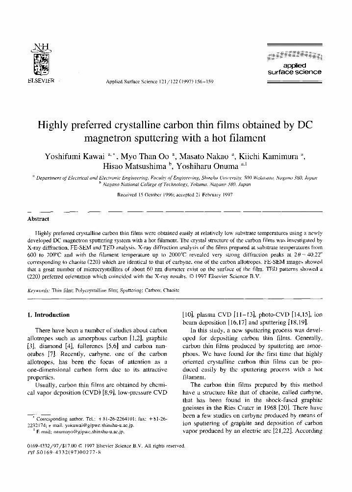
Field emission scanning electron microscopy (FE- SEM) have been employed to characterize the mi- crostructure of carbon thin films. Fig. 2 shows FE- SEM images of polycrystalline carbon produced at a substrate temperature of 600°C. Fig. 2(a) shows the images of a sample prepared without filament heat- ing. The grains of carbon were not observed under this condition and it was found that the film is of amorphous-carbon form. Fig. 2(b, c) show the im- ages of samples prepared at the filament temperature up to 2000°C. It can be seen that there are many clusters containing a number of microcrystallites on the surface of the carbon films. It can be estimated from the FE-SEM images that the grain sizes of the clusters and the microcrystallites are about 750 and 60 nm, respectively.
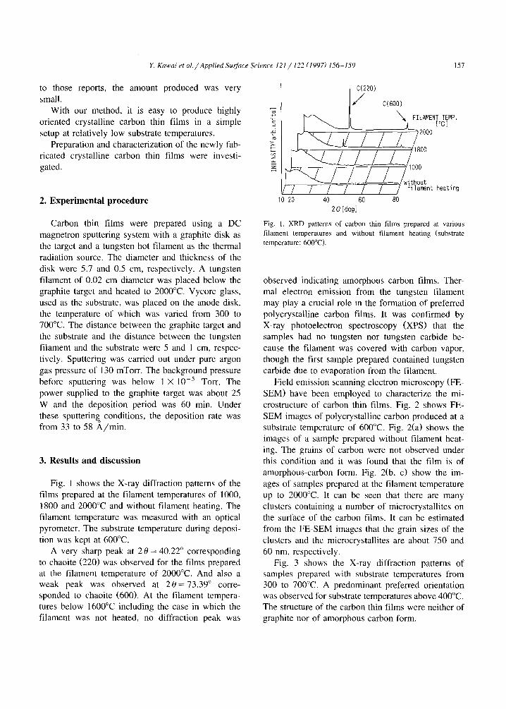
Fig. 3 shows the X-ray diffi-action patterns of samples prepared with substrate temperatures from 300 to 700°C. A predominant preferred orientation was observed for substrate temperatures above 400°C. The structure of the carbon thin films were neither of graphite nor of amorphous carbon form.
158 E Kawai et el./Applied Su~kwe Science 121 / 122 (1997) 156-159
(a)
I I
1.80 ZZ m
(b) I I
1.80/.z m
(c) I t
400 nm
Fig. 2. FE-SEM images of carbon thin films (substrate tempera- ture: 600°C). Filament temperature: (a) without heating, (b, c) 2000°C. Magnification: (a, b) X 10k, (c) x45k.
,j~220)
7 c
,4
z H
UBSTRATE EMP. [°C ] 70O
00
b
10 20 40 60 80 20Edeg]
Fig. 3. Dependence of XRD patterns of carbon thin films on substrate temperature (filament temperature: 2000°C).
{el
¢:)
Fig. 4. Typical TED patterns for carbon thin films (filament temperature: 2000°C). Substrate temperature: (a) 500°C, (b) 600°C.
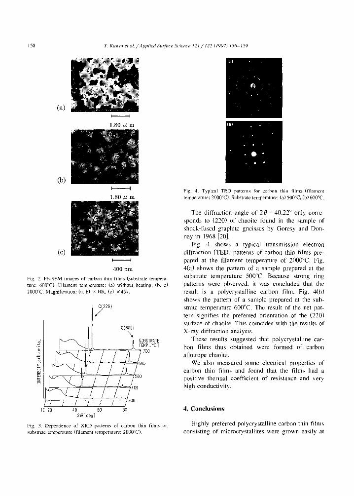
The diffraction angle of 2 0 = 40.22 ° only corre- sponds to (220) of chaoite found in the sample of shock-fused graphite gneisses by Goresy and Don- nay in 1968 [20].
Fig. 4 shows a typical transmission electron diffraction (TED) patterns of carbon thin films pre- pared at the filament temperature of 2000°C. Fig. 4(a) shows the pattern of a sample prepared at the substrate temperature 500°C. Because strong ring patterns were observed, it was concluded that the result is a polycrystalline carbon film. Fig. 4(b) shows the pattern of a sample prepared at the sub- strate temperature 600°C. The result of the net pat- tern signifies the preferred orientation of the (220) surface of chaoite. This coincides with the results of X-ray diffraction analysis.
These results suggested that polycrystalline car- bon films thus obtained were formed of carbon allotrope chaoite.
We also measured some electrical properties of carbon thin films and found that the films had a positive thermal coefficient of resistance and very high conductivity.
4. Conclusions
Highly preferred polycrystalline carbon thin films consisting of microcrystallites were grown easily at

E Kawai et al./Applied SurJiwe Science 121 / 122 (1997) 156-159 159
relatively low substrate temperature by the DC mag- netron sputtering technique with thermal electron emission using a tungsten hot filament for the first time in this study.
Carbon films thus obtained are considered to be a chaoite called carbyne, one of the carbon allotropes.
The mechanism of growth and the electrical prop- erties of the carbon films are now under investiga- tion. There are still many unknown factors, but these films are expected to be applicable to electronic devices as a new electronic material.
Acknowledgements
The authors would like to thank the referee for useful suggestions and comments.
References
[1] M. Morgan, Thin Solid Films 7 (1971) 313. [2] N.H. Cho, D.K. Veirs, J.W. Ager lII, M.D. Rubin, C.B.
Hopper, D.B. Boggy, J. Appl. Phys. 71 (1992) 2243. [3] S. Mrozowski, Phys. Rev. 77 (1950) 838.
[4] R. Ramesham, T. Roppel, J, Mater. Rev. 7 (1992) 1144. [5] H.W. Kroto, J.R. Heath, S.C. O'Brien, R.F. Curl, R.E.
Smalley, Nature 318 (1985) 162. [6] S. Saito, Kotai Butsuri 27 (1992) 51, in Japanese. [7] S. Iizima~ Nature 354 (1961) 56. [8] A.H. White, L.H. Germer, J. Chem, Phys. 9 (1941) 491. [9] Y. Onuma, T. Koyama, Oyo Buturi 11 (1963) 857, in
Japanese. [10] M.L. Kaplan, P.H. Schmidt, C.H. Chem W.M. Waish Jr.,
Appl. Phys. Lett. 36 (1980) 867. [11] Y. Onuma, Y. Kato, M. Nakao, H. Matsushima, Jpn. J. Appl.
Phys. 22 (1983) 888. [12] Y. Onuma, Y. Kato, M. Nakao, H. Matsushima, Shinku 26
(1983) 13, in Japanese. [13] K. Enke, Thin Solid Films 80 (1981) 227. [14] M. Danno, M. Hanabusa, Mater. gett. 4 (1986) 261. [15] H. Hanabusa, T. Kaneoka, J. Vac. Sci. Technol. B 5 (1987)
1432. [16] E.G, Spenser, P.H. Schmids, D.C. Joy, F.J. Sanalone. Phys.
gett. 29 (1976) I 18. [17] S. Aisengerg, R. Charot, J. Appl. Phys. 42 (1971) 2953. [18] N. Hosokawa, A. Konishi, H. Hiratsuka, A. Annoh, Thin
Solid Films 73 (1980) 115. [19] B.S. Chao, S.R. Ovshinsky, J. Appl. Phys. 78 (1995) 3015. [20] A. El Goresy, G. Donnay, Science 161 (1968) 363. [21] Y.P, Kudryavtsev, S.E. Evsyukov, V.G. Babaev, M.B. Gu-
seva, V.V. Khvostov, L.M. Krechko, Carbon 30 (1992) 213. [22] S. Tanuma, Kotai Butsuri 10 (1992) 59, in Japanese.