High Voltage, Isolated IGBT Gate Driver with Isolated ... · User Register Map ..... 15 User...
24
High Voltage, Isolated IGBT Gate Driver with Isolated Flyback Controller Data Sheet ADuM4138 Rev. 0 Document Feedback Information furnished by Analog Devices is believed to be accurate and reliable. However, no responsibility is assumed by Analog Devices for its use, nor for any infringements of patents or other rights of third parties that may result from its use. Specifications subject to change without notice. No license is granted by implication or otherwise under any patent or patent rights of Analog Devices. Trademarks and registered trademarks are the property of their respective owners. One Technology Way, P.O. Box 9106, Norwood, MA 02062-9106, U.S.A. Tel: 781.329.4700 ©2018 Analog Devices, Inc. All rights reserved. Technical Support www.analog.com FEATURES 6 A (typical) peak drive output capability Internal turn off NFET, on resistance: <1 Ω Internal turn on PFET, on resistance: <1.2 Ω 2 overcurrent protection methods Desaturation detection Split emitter overcurrent detection Miller clamp output with gate sense input Isolated fault output Isolated temperature sensor readback Propagation delay Rising: 95 ns typical Falling: 100 ns typical Minimum pulse width: 74 ns Operating junction temperature range: −40°C to +150°C VDD1 and VDD2 UVLO Minimum external tracking (creepage): 8.3 mm (pending) Safety and regulatory approvals 5000 V rms for 1 minute per UL 1577 CSA Component Acceptance Notice 5A DIN V VDE V 0884-10 (VDE V 0884-10):2006-12 VIORM = 849 VPEAK (reinforced/basic) Qualified for automotive applications APPLICATIONS MOSFET and IGBT gate drivers Photovoltaic (PV) inverters Motor drives Power supplies GENERAL DESCRIPTION The ADuM4138 is a single-channel gate driver optimized for driving insulated gate bipolar transistors (IGBTs). Analog Devices, Inc., iCoupler® technology provides isolation between the input signal and the output gate drive. The Analog Devices chip scale transformers also provide isolated communication of control information between the high voltage and low voltage domains of the chip. Information on the status of the chip can be read back from the dedicated outputs. The ADuM4138 includes an isolated flyback controller, allowing simple secondary voltage generation. Overcurrent detection is integrated in the ADuM4138 to protect the IGBT in case of desaturation and/or overcurrent events. The overcurrent detection is coupled with a high speed, two-level turn off function in case of faults. The ADuM4138 provides a Miller clamp control signal for a metal-oxide semiconductor field effect transistor (MOSFET) to provide IGBT turn off, with a single rail supply when the Miller clamp voltage threshold drops below 2 V (typical) above GND2. Operation with unipolar secondary supplies is possible with or without the Miller clamp operation. A low gate voltage detection circuit can trigger a fault if the gate voltage does not rise above the internal threshold within the time allowed after turn on (12.8 μs typical). The low voltage detection circuit detects IGBT device failures that exhibit gate shorts or other causes of weak drive. Two temperature sensor pins, TS1 and TS2, allow isolated monitoring of system temperatures at the IGBTs. The secondary undervoltage lockout (UVLO) is set to 11.2 V (typical) in accordance with common IGBT threshold levels. A serial peripheral interface (SPI) bus on the primary side of the device provides in field programming of temperature sensing diode gains and offsets to the ADuM4138. Values are stored on an electrically erasable programmable read-only memory (EEPROM) located on the secondary side of the device. In addition, programming is available for specific VDD2 voltages, temperature sensing reporting frequencies, and overcurrent blanking times. The ADuM4138 provides isolated fault reporting for overcurrent events, remote temperature overheating events, UVLO, thermal shutdown (TSD), and desaturation detection. Protected by U.S. Patents 5,952,849; 6,873,065; and 7,075,329. Other patents pending.
Transcript of High Voltage, Isolated IGBT Gate Driver with Isolated ... · User Register Map ..... 15 User...

High Voltage, Isolated IGBT Gate Driver with Isolated Flyback Controller
Data Sheet ADuM4138
Rev. 0 Document Feedback Information furnished by Analog Devices is believed to be accurate and reliable. However, no responsibility is assumed by Analog Devices for its use, nor for any infringements of patents or other rights of third parties that may result from its use. Specifications subject to change without notice. No license is granted by implication or otherwise under any patent or patent rights of Analog Devices. Trademarks and registered trademarks are the property of their respective owners.
One Technology Way, P.O. Box 9106, Norwood, MA 02062-9106, U.S.A.Tel: 781.329.4700 ©2018 Analog Devices, Inc. All rights reserved. Technical Support www.analog.com
FEATURES 6 A (typical) peak drive output capability Internal turn off NFET, on resistance: <1 Ω Internal turn on PFET, on resistance: <1.2 Ω 2 overcurrent protection methods
Desaturation detection Split emitter overcurrent detection
Miller clamp output with gate sense input Isolated fault output Isolated temperature sensor readback Propagation delay
Rising: 95 ns typical Falling: 100 ns typical
Minimum pulse width: 74 ns Operating junction temperature range: −40°C to +150°C VDD1 and VDD2 UVLO Minimum external tracking (creepage): 8.3 mm (pending) Safety and regulatory approvals
5000 V rms for 1 minute per UL 1577 CSA Component Acceptance Notice 5A DIN V VDE V 0884-10 (VDE V 0884-10):2006-12
VIORM = 849 VPEAK (reinforced/basic) Qualified for automotive applications
APPLICATIONS MOSFET and IGBT gate drivers Photovoltaic (PV) inverters Motor drives Power supplies
GENERAL DESCRIPTION The ADuM4138 is a single-channel gate driver optimized for driving insulated gate bipolar transistors (IGBTs). Analog Devices, Inc., iCoupler® technology provides isolation between the input signal and the output gate drive.
The Analog Devices chip scale transformers also provide isolated communication of control information between the high voltage
and low voltage domains of the chip. Information on the status of the chip can be read back from the dedicated outputs.
The ADuM4138 includes an isolated flyback controller, allowing simple secondary voltage generation.
Overcurrent detection is integrated in the ADuM4138 to protect the IGBT in case of desaturation and/or overcurrent events. The overcurrent detection is coupled with a high speed, two-level turn off function in case of faults.
The ADuM4138 provides a Miller clamp control signal for a metal-oxide semiconductor field effect transistor (MOSFET) to provide IGBT turn off, with a single rail supply when the Miller clamp voltage threshold drops below 2 V (typical) above GND2. Operation with unipolar secondary supplies is possible with or without the Miller clamp operation.
A low gate voltage detection circuit can trigger a fault if the gate voltage does not rise above the internal threshold within the time allowed after turn on (12.8 μs typical). The low voltage detection circuit detects IGBT device failures that exhibit gate shorts or other causes of weak drive.
Two temperature sensor pins, TS1 and TS2, allow isolated monitoring of system temperatures at the IGBTs. The secondary undervoltage lockout (UVLO) is set to 11.2 V (typical) in accordance with common IGBT threshold levels.
A serial peripheral interface (SPI) bus on the primary side of the device provides in field programming of temperature sensing diode gains and offsets to the ADuM4138. Values are stored on an electrically erasable programmable read-only memory (EEPROM) located on the secondary side of the device. In addition, programming is available for specific VDD2 voltages, temperature sensing reporting frequencies, and overcurrent blanking times.
The ADuM4138 provides isolated fault reporting for overcurrent events, remote temperature overheating events, UVLO, thermal shutdown (TSD), and desaturation detection.
Protected by U.S. Patents 5,952,849; 6,873,065; and 7,075,329. Other patents pending.

ADuM4138 Data Sheet
Rev. 0 | Page 2 of 24
TABLE OF CONTENTS Features .............................................................................................. 1 Applications ....................................................................................... 1 General Description ......................................................................... 1 Revision History ............................................................................... 2 Functional Block Diagram .............................................................. 3 Specifications ..................................................................................... 4
Electrical Characteristics ............................................................. 4 SPI Timing Specifications ........................................................... 7 Package Characteristics ............................................................... 7 Regulatory Information (Pending) ............................................ 8 Insulation and Safety-Related Specifications ............................ 8 DIN V VDE V 0884-10 (VDE V 0884-10) Insulation Characteristics (Pending) ............................................................ 9 Recommended Operating Conditions ...................................... 9
Absolute Maximum Ratings .......................................................... 10 Thermal Resistance .................................................................... 10 ESD Caution ................................................................................ 10
Pin Configuration and Function Descriptions ........................... 11 Typical Performance Characteristics ........................................... 12
Theory of Operation ...................................................................... 13 Applications Information .............................................................. 14
PCB Layout ................................................................................. 14 Isolated Flyback Controller ....................................................... 14 SPI and EEPROM Operation.................................................... 14 User Register Map ...................................................................... 15 User Register Bits ....................................................................... 15 Configuration Register Bits....................................................... 15 Control Register Bits .................................................................. 17 Propagation Delay Related Parameters ................................... 18 Protection Features .................................................................... 18 Power Dissipation....................................................................... 22 Insulation Lifetime ..................................................................... 22 DC Correctness and Magnetic Field Immunity ..................... 23 Typical Application Circuit ....................................................... 23
Outline Dimensions ....................................................................... 24 Ordering Guide .......................................................................... 24 Automotive Products ................................................................. 24
REVISION HISTORY 12/2018—Revision 0: Initial Version

Data Sheet ADuM4138
Rev. 0 | Page 3 of 24
FUNCTIONAL BLOCK DIAGRAM
2
3
1
17
20
22
27
26
ADuM4138 DECODE
DECODE
DECODE
15
21
16
19
18
28
FLYBACKCONTROLLER
LOGIC
23
24
VDD2
OC_DETDRIVE
MILLER_THRESH
FAULTVDD2
V2LEV
OC_DET FAULTDRIVE
LOW_T_OP
LOW_T_OP
VMILLER
MILLER_THRESH
VOC = 2V
Δt = tdOC
VOC_OFF
VOT
Δt = tdOT
OT_ERROR
EEPROM
SAWTOOTH
IT2
VLOW_TEMP
HYSTERESIS
LOW_T_OP
VDD1
9
25
VDD2
9V
Δt = tdDst
DESAT_ERROR
IDESAT
ENCODE
ENCODE
ENCODE
ENCODE
ENCODE
6
5UVLO1
FLYBACKCONTROLLER
LOGICVDD2_REF
7 FAIL LATCH= tDALM
UVLO2TSDDESAT_ERROROC_ERROROT_ERRORVL_ERROR
8
SPI
4
INTERNALLDO
REGULATOR
5V
VDD1
GAIN1VT_OFFSET1GAIN2VT_OFFSET2
VT_OFFSET1
GAIN1
VT_OFFSET2
GAIN2
IT1
TEMP_OUT_PWM
TEMP_OUT_PWM
VPGOODHYSTERESIS
DECODE
DECODE VVL
VL_ERROR
UVLO1
VUVLO1 HYSTERESIS
VDD1
UVLO1
SCALINGBLOCK
V5
INF
IPG
V5
V5
Δt = tVDD1
HYSTERESIS
TSD INTERNALTEMPERATURESENSOR
INTERNALLDO
REGULATOR5V
VDD2
SW
VI_SENSE
II_SENSE
ISENSE
GND1
VDD1
V5_1
VI+
FAULT
TEMP_OUT
PGOOD
MOSI
MISO
CS
SCLK
GND1
GND2
DESAT
VOUT_ON
VOUT_OFF
V5_2
VOFF_SOFT
GATE_SENSE
MILLER_OUT
OC1
OC2
TS1
TS2
GND2
FAULT
DRIVEFAULT
UVLO2
FAULT
DRIVE
DRIVEFAULT
OC_DET
OC_ERROR
VUVLO2HYSTERESIS
DRIVE
Δt = t DVL
14
11
10
12
13
1603
6-00
1NOTES1. VL_ERROR IS THE VOLTAGE LOW ERROR INTERNAL CONNECTION.2. TEMP_OUT_PWM IS THE TEMPERATURE SENSE INTERNAL CONNECTION.3. OC_ERROR IS THE OVERCURRENT ERROR INTERNAL CONNECTION.4. OC_DET IS THE OVERCURRENT DETECTION INTERNAL CONNECTION.5. VDD2_REF IS THE REFERENCE VOLTAGE FOR VDD2.6. DESAT_ERROR IS THE DESAT DETECTION ERROR INTERNAL CONNECTION.7. MILLER_THRESH IS THE REFERENCE FOR THE MILLER THRESHOLD ACTIVATION.8. OT_ERROR IS THE OVERTEMPERATURE ERROR INTERNAL CONNECTION.9. VT_OFFSET1 IS THE TEMPERATURE SENSE OFFSET VOLTAGE FOR THE TS1 PIN.10. VT_OFFSET2 IS THE TEMPERATURE SENSE OFFSET VOLTAGE FOR TS2 PIN.11. IT1 IS THE INTERNAL CURRENT REFERENCE FOR TS1 PIN.12. IT2 IS THE INTERNAL CURRENT REFERENCE FOR TS2 PIN.13. VOC_OFF IS THE OVERCURRENT VOLTAGE OFFSET DUE TO TEMPERATURE RAMP.14. VOC IS THE OVERCURRENT REFERENCE VOLTAGE.15. MILLER_THRESH IS THE ACTIVE MILLER CLAMP INTERNAL CONTROL CONNECTION.16. IOC1 IS THE OC1 INTERNAL PULL-UP CURRENT SOURCE.17. IOC2 IS THE OC2 INTERNAL PULL-UP CURRENT SOURCE.18. VPGOOD IS THE PGOOD VOLTAGE REFERENCE.19. VUVLO1 IS THE VDD1 UVLO REFERENCE.20. VLOW_TEMP IS THE LOW TEMPERATURE OPERATION REFERENCE.21. V2LEV IS THE TARGET VOLTAGE REFERENCE FOR TWO LEVEL OPERATION.22. LOW_T_OP IS THE LOW TEMPERATURE OPERATION TRIGGER.
IOC1
IOC2
UVLO2
Figure 1.

ADuM4138 Data Sheet
Rev. 0 | Page 4 of 24
SPECIFICATIONS ELECTRICAL CHARACTERISTICS Low-side voltages referenced to GND1 and high-side voltages referenced to GND2. VDD1 = 12 V, VDD2 = 16 V, TA = −40°C to +125°C, unless otherwise noted. All minimum and maximum specifications apply over the entire recommended operating junction temperature range, unless otherwise noted. All typical specifications are at TA = 25°C, VDD1 = 12 V, and VDD2 = 16 V, unless otherwise noted.
Table 1. Parameter Symbol Min Typ Max Unit Test Conditions/Comments DIGITAL CONVERTER SPECIFICATIONS
High-Side Power Supply Input Voltage VDD2 12 25 V Operating without flyback Input Current, Quiescent for VDD2 IDD2(Q) 14 18 mA TS1 = TS2 = open, VI+ = 0 V,
VDD2 = 25 V V5_2 Regulated Output Voltage V5_2 4.9 5 5.1 V
Isolated Flyback Soft Start tSS 44 50 ms Output Voltage VFB VDD2 −
2.6% VDD2 VDD2 +
2.5% V All FLYBACK_V codes
15.6 16 16.4 V For FLYBACK_V code of 0111 Flyback Operating Frequency fSW 180 200 220 kHz Maximum
Duty Cycle DMAX 83.5 86 90 % On Time tMAX_ON 4.2 4.8 5.4 µs
Flyback Switch RDSON Negative Channel Field Effect
Transistor (NFET) RDSON_SW_N 1.6 3.0 Ω SW current (ISW) = 20 mA
Positive Channel Field Effect Transistor (PFET)
RDSON_SW_P 1.7 2.8 Ω ISW = 20 mA
Logic Supply VDD1 Input Voltage VDD1 6.0 25 V V5_1 Regulated Output Voltage VV5_1 4.9 5.0 5.1 V No load VDD1 Input Current IDD1 4.0 5.0 mA TS1 = TS2 = open, VI+ = 0 V,
TEMP_OUT and SW floating, VDD1 = 25 V, VDD2 = 25 V
Logic Inputs (VI+, MOSI, SCLK, CS)
Input Current II 0.1 1.0 µA Input Voltage
Logic High VIH 2.5 V Logic Low VIL 0.9 V
Logic Input Hysteresis VHYST 1.10 V Logic Output
MISO NFET RDSON RDSON_MISO_N 9 16 Ω MISO current (IMISO) = 5 mA MISO PFET RDSON RDSON_MISO_P 12.5 22 Ω IMISO = 5 mA MISO PFET High-Z Leakage IMISO_LK_P 20.0 µA MISO = 5 V
UVLO Positive Going Threshold
VDD1 VVDD1UV+ 4.25 4.5 V VDD2 VVDD2UV+ 11.6 11.8 V
Negative Going Threshold VDD1 VVDD1UV− 4.0 4.13 V VDD2 VVDD2UV− 11.0 11.2 V
Hysteresis VDD1 VVDD1UVH 0.1 V VDD2 VVDD2UVH 0.3 V
Data Sheet ADuM4138
Rev. 0 | Page 5 of 24
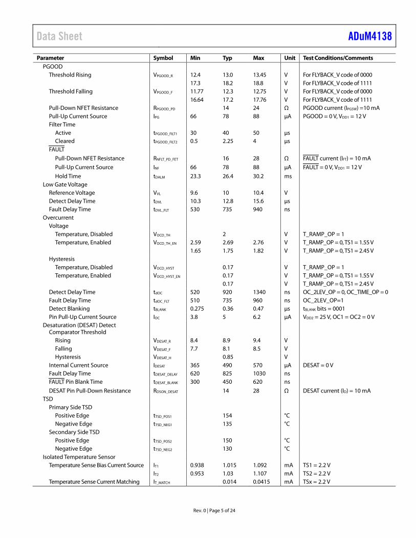
Parameter Symbol Min Typ Max Unit Test Conditions/Comments PGOOD
Threshold Rising VPGOOD_R 12.4 13.0 13.45 V For FLYBACK_V code of 0000 17.3 18.2 18.8 V For FLYBACK_V code of 1111 Threshold Falling VPGOOD_F 11.77 12.3 12.75 V For FLYBACK_V code of 0000 16.64 17.2 17.76 V For FLYBACK_V code of 1111 Pull-Down NFET Resistance RPGOOD_PD 14 24 Ω PGOOD current (IPGSW) =10 mA Pull-Up Current Source IPG 66 78 88 µA PGOOD = 0 V, VDD1 = 12 V Filter Time
Active tPGOOD_FILT1 30 40 50 µs Cleared tPGOOD_FILT2 0.5 2.25 4 µs
FAULT
Pull-Down NFET Resistance RNFLT_PD_FET 16 28 Ω FAULT current (IFT) = 10 mA
Pull-Up Current Source INF 66 78 88 µA FAULT = 0 V, VDD1 = 12 V
Hold Time tDALM 23.3 26.4 30.2 ms Low Gate Voltage
Reference Voltage VVL 9.6 10 10.4 V Detect Delay Time tDVL 10.3 12.8 15.6 µs Fault Delay Time tDVL_FLT 530 735 940 ns
Overcurrent Voltage
Temperature, Disabled VOCD_TH 2 V T_RAMP_OP = 1 Temperature, Enabled VOCD_TH_EN 2.59 2.69 2.76 V T_RAMP_OP = 0, TS1 = 1.55 V
1.65 1.75 1.82 V T_RAMP_OP = 0, TS1 = 2.45 V Hysteresis
Temperature, Disabled VOCD_HYST 0.17 V T_RAMP_OP = 1 Temperature, Enabled VOCD_HYST_EN 0.17 V T_RAMP_OP = 0, TS1 = 1.55 V
0.17 V T_RAMP_OP = 0, TS1 = 2.45 V Detect Delay Time tdOC 520 920 1340 ns OC_2LEV_OP = 0, OC_TIME_OP = 0 Fault Delay Time tdOC_FLT 510 735 960 ns OC_2LEV_OP=1 Detect Blanking tBLANK 0.275 0.36 0.47 µs tBLANK bits = 0001 Pin Pull-Up Current Source IOC 3.8 5 6.2 µA VDD2 = 25 V, OC1 = OC2 = 0 V
Desaturation (DESAT) Detect Comparator Threshold
Rising VDESAT_R 8.4 8.9 9.4 V
Falling VDESAT_F 7.7 8.1 8.5 V Hysteresis VDESAT_H 0.85 V
Internal Current Source IDESAT 365 490 570 µA DESAT = 0 V Fault Delay Time tDESAT_DELAY 620 825 1030 ns FAULT Pin Blank Time tDESAT_BLANK 300 450 620 ns
DESAT Pin Pull-Down Resistance RDSON_DESAT 14 28 Ω DESAT current (ID) = 10 mA TSD
Primary Side TSD Positive Edge tTSD_POS1 154 °C Negative Edge tTSD_NEG1 135 °C
Secondary Side TSD Positive Edge tTSD_POS2 150 °C Negative Edge tTSD_NEG2 130 °C
Isolated Temperature Sensor Temperature Sense Bias Current Source IT1 0.938 1.015 1.092 mA TS1 = 2.2 V IT2 0.953 1.03 1.107 mA TS2 = 2.2 V Temperature Sense Current Matching IT_MATCH 0.014 0.0415 mA TSx = 2.2 V

ADuM4138 Data Sheet
Rev. 0 | Page 6 of 24
Parameter Symbol Min Typ Max Unit Test Conditions/Comments Pulse-Width Modulation (PWM) Output
Frequency fPWM 9.20 10 10.80 kHz PWM_OSC = 0, TSx = 2.2 V 46 50 54 kHz PWM_OSC = 1, TSx = 2.2 V
PWM Duty Cycle TSx = 2.45 V 7.50 10 11.3 % PWM_OSC = 0 TSx = 2.25 V 26 28 29.5 % PWM_OSC = 0 TSx = 1.55 V 90.2 92 93.3 % PWM_OSC = 0 TSx = 2.45 V 7.5 10 11.5 % PWM_OSC = 1 TSx = 2.25 V 26 28 29.6 % PWM_OSC = 1 TSx = 1.55 V 90.1 92 93.3 % PWM_OSC = 1
Overtemperature Detect Delay Time tDOT 0.80 1 1.2 ms Fault Delay Time tDOT_FLT 530 735 940 ns Detection Voltage
Rising VOT_0_R 1.62 1.69 1.73 V OT_FAULT_SEL = 0 VOT_1_R 1.63 1.73 1.81 V OT_FAULT_SEL = 1 Falling VOT_0_F 1.57 1.65 1.70 V OT_FAULT_SEL = 0
VOT_1_F 1.59 1.69 1.78 V OT_FAULT_SEL = 1 Low Temperature Threshold
Rising VLOW_T_R 2.35 2.4 2.45 V TS1 pin voltage Falling VLOW_T_F 2.31 2.36 2.41 V TS1 pin voltage
TEMP_OUT Resistance Pull-Down RTEMP_N 11.3 20 Ω TEMP_OUT current (ITEMP_OUT) = 5 mA Pull-Up RTEMP_P 13.7 23 Ω ITEMP_OUT = 5 mA
Miller Clamp Voltage Threshold VMILLER 1.9 2 2.1 V Referenced to GND2 Internal Turn Off NFET
On Resistance RDSON_N 0.5 1 Ω VOUT_OFF current (IVOUT_OFF) = 0.5 A, VDD1 = 6 V, VDD2 = 12 V
On Resistance 2 Level RDSON_N_2LEV 1.8 4 Ω IVOUT_OFF = 0.1 A, VDD1 = 6 V, VDD2 = 12 V Internal Turn On PFET
On Resistance RDSON_P 0.6 1.2 Ω VOUT_ON current (IVOUT_ON) = 0.5 A, VDD1 = 6 V, VDD2 = 12 V
On Resistance 2 Level RDSON_P_2LEV 2.0 4 Ω IVOUT_ON = 0.1 A, VDD1 = 6 V, VDD2 = 12 V
Miller Pull-Down NFET RDSON_MILLER 4.2 10 Ω Miller current (IMILLER) = 10 mA VOFF_SOFT RDSON RDSON_SOFT_OFF 15 36 Ω VOFF_SOFT current (IOFF_SOFT) = 10 mA Peak Current IPEAKIP 6 A VDD2 = 15 V, 2 Ω external resistance Two-Level Plateau Voltage V2LEV 11.30 11.90 12.50 V
CURRENT LIMIT Set Current II_SENSE 18 20 22 µA ISENSE = 0.5 V Internal Current-Limit Reference VI_SENSE 480 500 520 mV Rising edge Current-Limit Blanking Time tCL_BLANK 120 145 180 ns
SWITCHING SPECIFICATIONS Pulse Width1 PW 74 ns No load, Miller clamp open Propagation Delay
Rising2 tDLH 71 95 130 ns No load, Miller clamp open Falling2 tDHL 79 100 121 ns No load, Miller clamp open
1 The minimum pulse width is the shortest pulse width at which the specified timing parameter is guaranteed. 2 tDLH propagation delay is measured from the time of the input rising logic high threshold, VIH, to the output rising 0% level of the VOUT_ON or VOUT_OFF signal. tDHL
propagation delay is measured from the input falling logic low threshold, VIL, to the output falling 90% threshold of the VOUT_ON or VOUT_OFF signal. See Figure 13 for waveforms of propagation delay parameters.

Data Sheet ADuM4138
Rev. 0 | Page 7 of 24
SPI TIMING SPECIFICATIONS SPI timing specifications are guaranteed by design. All devices are production tested with 200 kHz SPI communication.
Table 2. Parameter Description Min Typ Max Unit tS Time to first clock edge 8 μs tDS Set period 1 μs tDH Hold period 1 μs tCLK Clock period 5 μs tH Release time 8 μs tHIGH Clock time high 100 ns tLOW Clock time low 100 ns tOV Output valid time 240 ns
SPI Timing Diagram
CS
SCLK
MOSI
MISO HIGH-Z
DON’T CARE MBZ RW0 A1 A0 MBZ
DON’T CARE
DON’T CARE
DON’T CARE
DON’T CARE
MBZ MBZ MBZ D23
0 RW0′ A1′ A0′ 0 0 0 0 D5′ D4′ D3′ D1′ D0′
D1 D0
D23′
D5 D4 D3
tCLK
tLOW
tOV
tDH
tHIGHtDS
tS tH
1603
6-00
4
Figure 2. SPI Timing Diagram
PACKAGE CHARACTERISTICS
Table 3. Parameter Symbol Min Typ Max Unit Resistance (Input Side to High-Side Output)1 RI-O 1012 Ω Capacitance (Input Side to High-Side Output)1 CI-O 2 pF Input Capacitance CI 4 pF 1 The device is considered a two terminal device: Pin 1 through Pin 14 are shorted together, and Pin 15 through Pin 28 are shorted together.

ADuM4138 Data Sheet
Rev. 0 | Page 8 of 24
REGULATORY INFORMATION (PENDING)
Table 4. UL (Pending) CSA (Pending) VDE (Pending) CQC (Pending)
UL1577 Component Recognition Program
Approved under CSA Component Acceptance Notice 5A
DIN V VDE V 0884-10 (VDE V 0884-10):2006-12
Certified under CQC11-471543-2012
Single Protection, 5000 V rms Isolation Voltage
CSA 60950-1-07+A1+A2 and IEC 60950-1, second edition, +A1+A2:
Reinforced insulation, 849 VPEAK, VIOTM = 8 kVPEAK
GB4943.1-2011
Basic insulation at 830 V rms (1174 VPEAK)
Basic insulation, 830 V rms (1174 VPEAK)
Reinforced insulation at 415 V rms (587 VPEAK)
Reinforced insulation, 415 V rms (587 VPEAK)
IEC 60601-1 Edition 3.1:
Basic insulation (1 MOPP), 519 V rms (734 VPEAK)
Reinforced insulation (2 MOPP), 261 V rms (369 VPEAK)
CSA 61010-1-12 and IEC 61010-1 third edition
Basic insulation, 300 V rms mains, 830 V secondary (1174 VPEAK)
Reinforced insulation, 300 V rms mains, 415 V secondary (587 VPEAK)
File E214100 File 205078 File 2471900-4880-0001 File (pending)
INSULATION AND SAFETY-RELATED SPECIFICATIONS
Table 5. Parameter Symbol Value Unit Test Conditions/Comments Rated Dielectric Insulation Voltage 5000 V rms 1 minute duration Minimum External Air Gap (Clearance) L (I01) 8.3 mm min Measured from input terminals to output
terminals, shortest distance through air Minimum External Tracking (Creepage) L (I02) 8.3 mm min Measured from input terminals to output
terminals, shortest distance path along body Minimum Clearance in the Plane of the Printed
Circuit Board (PCB Clearance) L (PCB) 8.7 mm min Measured from input terminals to output
terminals, shortest distance through air, line of sight, in the PCB mounting plane
Minimum Internal Gap (Internal Clearance) 0.017 mm min Insulation distance through insulation Tracking Resistance (Comparative Tracking Index) CTI >400 V DIN IEC 112/VDE 0303 Part 1 Material Group II Material group (DIN VDE 0110, 1/89, Table 1)

Data Sheet ADuM4138
Rev. 0 | Page 9 of 24
DIN V VDE V 0884-10 (VDE V 0884-10):2016-12 INSULATION CHARACTERISTICS (PENDING) These isolators are suitable for reinforced isolation only within the safety limit data. Protective circuits ensure the maintenance of the safety data. The asterisk (*) marking on the package denotes DIN V VDE V 0884-10 approval for a 560 VPEAK working voltage.
Table 6. VDE Characteristics Description Test Conditions/Comments Symbol Characteristic Unit Installation Classification per IEC 60664-1 For Rated Mains Voltage ≤ 150 V rms I to IV For Rated Mains Voltage ≤ 300 V rms I to IV For Rated Mains Voltage ≤ 600 V rms I to IV Climatic Classification 40/125/21 Pollution Degree per DIN VDE 0110, Table 1 2 Maximum Working Insulation Voltage VIORM 849 VPEAK Input to Output Test Voltage, Method B1 VIORM × 1.875 = Vpd(m), 100% production test,
tini = tm = 1 sec, partial discharge < 5 pC Vpd(m) 1592 VPEAK
Input to Output Test Voltage, Method A VIORM × 1.5 = Vpd(m), tini = 60 sec, tm = 10 sec, partial discharge < 5 pC
Vpd(m)
After Environmental Tests Subgroup 1 1274 VPEAK After Input and/or Safety Test
Subgroup 2 and Subgroup 3 VIORM × 1.2 = Vpd(m), tini = 60 sec, tm = 10 sec, partial discharge < 5 pC
1019 VPEAK
Highest Allowable Overvoltage VIOTM 8000 VPEAK Impulse 1.2 µs rise time, 50 µs, 50% fall time in air to the
preferred sequence VIMPULSE 8000 VPEAK
Surge Isolation Voltage Basic VPEAK = 12.8 kV, 1.2 µs rise time, 50 µs, 50% fall time VIOSM 9800 VPEAK Surge Isolation Voltage Reinforced VPEAK = 12.8 kV, 1.2 µs rise time, 50 µs, 50% fall time VIOSM 8000 VPEAK Safety Limiting Values Maximum value allowed in the event of a
failure (see Figure 3)
Maximum Junction Temperature TS 150 °C Total Power Dissipation at TA = 25°C PS 2.0 W
Insulation Resistance at TS Voltage between the input and output (VIO) = 500 V RS >109 Ω
AMBIENT TEMPERATURE (°C)
0 50 100 150 200
SAFE
OPE
RATI
NG
PVD
D1,
PO
WER
(W)
2.5
2.0
1.5
1.0
0.5
0
1603
6-00
2
Figure 3. Thermal Derating Curve, Dependence of Safety Limiting Values on
Case Temperature, per DIN V VDE V 0884-10
RECOMMENDED OPERATING CONDITIONS
Table 7. Parameter Value Operating Junction Temperature Range −40°C to +150°C Supply Voltages
VDD1 Referenced to GND1 6.0 V to 25 V VDD2 Referenced to GND2 12 V to 25 V

ADuM4138 Data Sheet
Rev. 0 | Page 10 of 24
ABSOLUTE MAXIMUM RATINGS Table 8. Parameter Rating Supply Voltages
VDD1 −0.2 V to +30 V VDD2 −0.2 V to +30 V
Primary Side Pins VI+, MOSI, CS, SCLK −0.2 V to +5.5 V
SW, ISENSE, FAULT, TEMP_OUT, PGOOD, MISO
−0.2 V to V5_1 + 0.2 V
Secondary Side Pins TS1, TS2 −0.2 V to V5_2 + 0.2 V MILLER_OUT, VOFF_SOFT, VOUT_OFF −0.2 V to + 30 V VOUT_ON, DESAT, GATE_SENSE,
OC1, OC2 −0.2 V to VDD2 + 0.2 V
Common-Mode Transients (|CM|) −150 kV/µs to +150 kV/µs Storage Temperature Range (TST) −55°C to +150°C Operating Junction Temperature
Range −40°C to +150°C
Electrostatic Discharge (ESD) Human Body Model (HBM) ±1 kV Charge Device Model (CDM) ±1.25 kV
Stresses at or above those listed under Absolute Maximum Ratings may cause permanent damage to the product. This is a stress rating only; functional operation of the product at these or any other conditions above those indicated in the operational section of this specification is not implied. Operation beyond the maximum operating conditions for extended periods may affect product reliability.
THERMAL RESISTANCE Thermal performance is directly linked to PCB design and operating environment. Careful attention to PCB thermal design is required.
θJA is the junction to ambient thermal resistance, and ΨJT is the junction to top characterization parameter.
Table 9. Thermal Resistance Package Type1 θJA ΨJT Unit RN-28-1 62.4 2.97 °C/W
1 4-layer PCB.
ESD CAUTION
Table 10. Maximum Continuous Working Voltage1, 2, 3
Parameter Rating Constraint AC Voltage
Bipolar Waveform Basic Insulation 849 VPEAK Lifetime limited by insulation lifetime per VDE-0884-11 Reinforced Insulation 707 VPEAK Lifetime limited by insulation lifetime per VDE-0884-11
Unipolar Waveform Basic Insulation 1697 VPEAK Lifetime limited by insulation lifetime per VDE-0884-11 Reinforced Insulation 892 VPEAK Lifetime limited by package creepage per IEC 60664-1
DC Voltage Basic Insulation 1092 VPEAK Lifetime limited by package creepage per IEC 60664-1 Reinforced Insulation 546 VPEAK Lifetime limited by package creepage per IEC 60664-1
1 See the Insulation Lifetime section for details. 2 Other pollution degree and material group requirements yield a different limit. 3 Some system level standards allow components to use the printed wiring board (PWB) creepage values. The supported dc voltage may be higher for those standards.
Table 11. Truth Table (Positive Logic) VI+ Input FAULT Pin VDD1 State VDD2 State GATE_SENSE Voltage (VGATE_SENSE) Low High Powered Powered Low High High Powered Powered High Don’t Care or Unknown Low Powered Powered Low Don’t Care or Unknown Don’t care or unknown Unpowered Powered Low Don’t Care or Unknown Low Powered Unpowered High-Z

Data Sheet ADuM4138
Rev. 0 | Page 11 of 24
PIN CONFIGURATION AND FUNCTION DESCRIPTIONS VDD2
GND2
VOUT_ON
VOUT_OFF
V5_2
VOFF_SOFT
MILLER_OUT
DESAT
GATE_SENSE
OC1
OC2
GND2
TS1
TS2
SW
GND1
V5_1
VI+
CS
MOSI
ISENSE
SCLK
VDD1
PGOOD
FAULT
TEMP_OUT
GND1
MISO
1
2
3
4
5
6
7
8
9
10
11
12
13
14
28
27
26
25
24
23
22
21
20
19
18
17
16
15
ADuM4138
(Not to Scale)TOP VIEW
1603
6-00
3
Figure 4. Pin Configuration
Table 12. Pin Function Descriptions Pin No. Mnemonic Description 1 SW Switching Signal Pin for Isolated Flyback Converter. Connect this pin to the flyback transformer MOSFET. 2 ISENSE Flyback Current Sense. Current sense node for flyback transistor. 3 GND1 Ground Reference for Primary Side. Decouple this pin to VDD1. 4 VDD1 Input Supply Voltage Pin on Primary Side, 6 V to 25 V Referenced to GND1. 5 V5_1 5 V Regulated Output. Connect this pin to a 1 μF external capacitor referenced to GND1. This pin controls the
logic levels for the input pins. 6 VI+ Noninverting Input for Gate Drive. Connect this pin to the incoming PWM control signal. 7 FAULT Fault Reporting Pin. The FAULT pin goes low when an overcurrent event is detected by the overcurrent pin,
desaturation is detected, secondary UVLO occurs during thermal shutdown, during remote sensing overtemperature, or during gate voltage low errors.
8 TEMP_OUT Remote Temperature Sense Reporting Pin. This pin is 10 kHz or 50 kHz and is the 5% to 95% PWM output for the diode temperature sensor.
9 PGOOD Power Good Pin. The signal is high when the output voltage is within regulation. When not in use, leave this pin open.
10 MOSI Master Out, Slave In Pin. This pin provides the MOSI connection for the SPI bus. 11 MISO Master In, Slave Out Pin. This pin provides the MISO connection for the SPI bus. 12 CS Chip Select for SPI Bus. Logic is active low.
13 SCLK Clock for SPI Bus. Connect this pin to the clock pin from the SPI master. 14 GND1 Ground Reference for Primary Side. 15 GND2 Secondary Ground Reference. Use this ground pin for the high current path. 16 TS2 Remote Temperature Sensor 2. Float or pull this pin high to V5_2 when not in use. 17 TS1 Remote Temperature Sensor 1. See the Applications Information section for more information if this pin is unused. 18 OC2 Split Emitter Overcurrent Detection 2. Connect this pin to GND2 when this pin is not in use. 19 OC1 Split Emitter Overcurrent Detection 1. Connect this pin to GND2 when this pin is not in use. 20 MILLER_OUT Output Signal to Control External MOSFET for Miller Clamping. 21 GATE_SENSE Miller Clamping Sense Pin. Connect this pin directly to the gate of the IGBT. 22 VOFF_SOFT Soft Shutdown Gate Connection. Connect this pin to the gate through the external series resistor. This pin
pulls the gate down during fault conditions. 23 VOUT_OFF Turns Off Current Path Connection. Connect this pin to the gate through the external series resistor. This pin
pulls the gate down during the low output command. 24 VOUT_ON Turns On Current Path Connection. Connect this pin to the gate through the external series resistor. This pin
pulls the gate up during the high output command. 25 DESAT Desaturation Detection Pin. Connect this pin to GND2 when not in use. 26 V5_2 5 V Regulated Output on Secondary Side. Connect this pin to the 1 μF external capacitor referenced to GND2. 27 GND2 Ground Reference for Secondary Side. 28 VDD2 Input Supply Voltage on Secondary Side, 15 V (Typical) Referenced to GND2.

ADuM4138 Data Sheet
Rev. 0 | Page 12 of 24
TYPICAL PERFORMANCE CHARACTERISTICS
1603
6-03
0CH1 5.00V CH2 5V 500ns/DIV 5.0GSPS
200ps PER POINTA CH1 3.3V
1
2
T VI+
GATE_SENSE
Figure 5. Example Turn On Edge, VDD1 = 12 V, VDD2 = 16 V, 3 Ω Turn On, 100 nF Load
1603
6-03
1
CH1 5.00V CH2 5V 500ns/DIV 5.0GSPS200ps PER POINT
A CH1 3.3V
1
2
T
VI+
GATE_SENSE
Figure 6. Example Turn Off Edge, VDD1 = 12 V, VDD2 = 16 V, 2 Ω Turn Off, 100 nF Load
1603
6-03
2
CH1 3.0VCH3 5.0V
CH2 5.0V 5µs/DIV 5.0GSPS200ps PER POINT
A CH3 1.8V
1
2
3
T OC1
GATE_SENSE
FAULT
Figure 7. Example Overcurrent Fault, VDD1 = 12 V, VDD2 = 16 V, VI+ = 5 V, 2 Ω Turn Off, 100 nF Load
1603
6-03
3
CH1 5.0VCH3 5.0V
CH2 5.0V 10µs/DIV 5.0GSPS200ps PER POINT
A CH3 1.8V
1
2
3
T
GATE_SENSE
FAULT
DESAT
Figure 8. Example DESAT Fault, VDD1 = 12 V, VDD2 = 16 V, VI+ = 5 V, 2 Ω Turn Off, 100 nF Load
1603
6-03
4
CH1 10.0VCH3 5.0V
CH2 10.0V 5ms/DIV 5.0MSPS500ns PER POINT
A CH1 5.4V
1
2
3
T
VDD2
FAULT
VDD1
Figure 9. Typical Flyback Startup, VDD1 = 12 V
1603
6-03
5
CH1 10.0VCH3 5.0V
CH2 10.0VCH4 5.0V
50µs/DIV 200MSPS5.0ns PER POINT
A CH4 2.2V
1
2
3
4
T
VDD2
FAULT
TEMP_OUT
VDD1
Figure 10. Example TEMP_OUT Reading, VDD1 = 12 V, VDD2 = 16 V

Data Sheet ADuM4138
Rev. 0 | Page 13 of 24
THEORY OF OPERATION Gate drivers are required in situations where fast rise times of switching device gates are required. The gate signals for enhancement power devices are referenced to a source or emitter node. The gate driver must follow this source or emitter node. As such, isolation is necessary between the controlling signal and the output of the gate driver in topologies where the source or emitter nodes swing, such as a half bridge. Gate switching times are a function of the drive strength of the gate driver. Buffer stages before a complementary metal-oxide semiconductor (CMOS) output reduce the total delay time and increase the final drive strength of the driver.
The ADuM4138 achieves isolation between the control side and the output side of the gate driver using a high frequency carrier that transmits data across the isolation barrier with iCoupler
chip scale transformer coils separated by layers of polyimide isolation. The ADuM4138 uses positive logic on/off keying (OOK) encoding, in which a high signal is transmitted by the presence of the carrier frequency across the iCoupler chip scale transformer coils. Positive logic encoding ensures that a low signal is seen on the output when the input side of the gate driver is unpowered. A low state is the most common safe state in enhancement mode power devices and can drive in situations where shoot through conditions are present. The architecture of the ADuM4138 is designed for high common-mode transient immunity and high immunity to electrical noise and magnetic interference. Radiated emissions are minimized with a spread spectrum OOK carrier and differential coil layout. Figure 11 shows the OOK encoding used by the ADuM4138.
TRANSMITTER
GND1 GND2
VI+
RECEIVER
REGULATOR REGULATOR
VOUT_ON
VOUT_OFF
1603
6-02
4
Figure 11. Operational Block Diagram of OOK Encoding
ADuM4138 Data Sheet
Rev. 0 | Page 14 of 24
APPLICATIONS INFORMATION PCB LAYOUT The ADuM4138 IGBT gate driver requires no external interface circuitry for the logic interfaces. Power supply bypassing is required at the VDD1 and VDD2 supply pins. Use a small ceramic capacitor (>10 µF) from VDD1 to GND1. Add at least 30 µF to 60 µF capacitance on the output power supply pin (VDD2) to provide the charge required to drive the gate capacitance at the outputs. This capacitance can be provided by multiple parallel capacitors. Avoid using vias on VDD2 on the bypass capacitor or employing multiple vias to reduce the inductance in bypassing because board vias can introduce parasitic inductance. The total lead length between both ends of the smaller capacitor and the input or output power supply pin must not exceed approximately 5 mm. For the 5 V regulators, place 1 µF capacitors as close as possible to the ADuM4138.
ISOLATED FLYBACK CONTROLLER The ADuM4138 has an integrated isolated flyback controller that delivers isolated power to the gate being driven. The flyback controller provides a control signal to the flyback MOSFET on the low side of the device. This MOSFET switches the primary side of the flyback transformer. An external diode rectifies the secondary voltage and regulates the internal compensation on the secondary side. An inductive isolation link transfers duty cycle information to the primary side.
Startup includes a soft start, where the duty cycle is controlled to a maximum value that increases with time. The primary side has an oscillator that controls this timing. The secondary side also has an oscillator, creating the 200 kHz (typical) ramp signal used to create the PWM control. The handoff between the soft start and secondary oscillator is controlled internally without user intervention. An internal resistor network performs feedback sensing on the VDD2 pin.
The power good pin, PGOOD, is available for output on the primary side, allowing the user to observe when the secondary voltage is within regulation.
If VDD2 loses power during operation, a fault posts to the primary side, and the flyback does not automatically attempt recovery. The VDD1 power cycle initiates the flyback operation again.
Peak current mode control is employed on the primary side of the ADuM4138 through the ISENSE pin. Use the following equation to set the current limit:
IPEAK (mA) = 100 mV/RS (1)
where: IPEAK is the desired peak current limit in mA. RS is the sense resistor used to set the peak current limit in Ω.
A typical application is shown in Figure 30. The recommended current-limit resistance (RCL) value is 20 kΩ. In operation, the equation for setting the peak current follows:
VI_SENSE = (II_SENSE) × (RCL) + (IPEAK) × (RS) (2)
where: VI_SENSE = 500 mV (typical) II_SENSE = 20 µA (typical) RCL = 20 kΩ (recommended)
SPI AND EEPROM OPERATION SPI Programming
The ADuM4138 contains an SPI bus for setting remote temperature gains and offsets, PWM reporting frequency, high temperature faults, and low temperature operation mode. The SPI bus allows programming of the secondary side EEPROM, allowing a permanent operation setting. The SPI interface can operate in a daisy-chain mode to allow efficient use of the microcontroller input and output pins. When the chip select (CS) pin is brought low, programming of the EEPROM is available. However, the gate drive output is disabled. The gate drive output is not available again until CS is brought back to high.
Programming is performed using the standard SPI convention of clock polarity (CPOL) = 0 and clock phase (CPHA) = 1. The SPI timing diagram shown in Figure 2 demonstrates a typical read or write operation. Bit A1 and Bit A0 are the address bits. The must be zero (MBZ) bits must be set to 0. Bits[D23:D0] are the data bits, with MSB first. Bit RW0 sets whether the action is a read (0) or a write (1).

Data Sheet ADuM4138
Rev. 0 | Page 15 of 24
USER REGISTER MAP Figure 12 shows the user register map and binary addresses.
ADDRESS NAME
00 USER OFFSET_2[5:0] GAIN_2[5:0] OFFSET_1[5:0] GAIN_1[5:0]
01 CONFIG RESERVED
RESERVED
OT
_FA
UL
T_O
P
OT
_FA
UL
T_S
EL
OC
_TIM
E_O
P
OC
_2L
EV
_OP
LO
W_T
_OP
OC
_BL
AN
K_O
P
t BL
AN
K[0
:3]
FL
YB
AC
K_V
[3:0
]
EC
C2_
SN
G_E
RR
EC
C2_
DB
L_E
RR
EC
C1_
SN
G_E
RR
EC
C1_
DB
L_E
RR
SIM
_TR
IM
PR
OG
_BU
SY
EC
C_O
FF
_OP
T_R
AM
P_O
P
PW
M_O
SC
10 CONTROL
BIT
23 22 21 20 19 18 17 16 15 14 13 12 11 10 9 8 7 6 5 4 3 2 1 0
1603
6-00
5
Figure 12. User Register Map
USER REGISTER BITS Table 13 lists the user register (Address 00) bits and bit descriptions.
Table 13. User Register (Address 00) Bit Descriptions Bits Bit Name Description [23:18] OFFSET_2[5:0] TS2 offset [17:12] GAIN_2[5:0] TS2 gain [11:6] OFFSET_1[5:0] TS1 offset [5:0] GAIN_1[5:0] TS1 gain
OFFSET_2[5:0] Bits
Use the OFFSET_2 bits of the EEPROM to adjust the internal offset for the TS2 pin.
GAIN_2[5:0] Bits
Use the GAIN_2 bits of the EEPROM to adjust the internal gain for the TS2 pin.
OFFSET_1[5:0] Bits
Use the OFFSET_1 bits of the EEPROM to adjust the internal offset for the TS1 pin.
GAIN_1[5:0] Bits
Use the GAIN_1 bits of the EEPROM to adjust the internal gain for the TS1 pin.
CONFIGURATION REGISTER BITS Table 14 lists the configuration (CONFIG) register (Address 01) bits and bit descriptions.
Table 14. CONFIG Register (Address 01) Bit Descriptions Bit Name Bits Description Reserved [23:17] Reserved OT_FAULT_OP 16 Overtemperature fault disable OT_FAULT_SEL 15 Overtemperature fault select OC_TIME_OP 14 Disable two-level drive and timer
during overcurrent event OC_2LEV_OP 13 Overcurrent two-level operation select LOW_T_OP 12 Low temperature operation select
Bit Name Bits Description OC_BLANK_OP 11 Overcurrent blanking operation select tBLANK[3:0] [10:7] Overcurrent blanking time ECC_OFF_OP 6 Enable soft shutdown with error
correcting code (ECC) fault FLYBACK_V[3:0] [5:2] Flyback output voltage setting T_RAMP_OP 1 Overcurrent temperature ramp enable PWM_OSC 0 Temperature reading output
oscillator select
OT_FAULT_OP Bit
Set the OT_FAULT_OP bit to 1 to disable a fault for over-temperature. If this bit is set to 0, the ADuM4138 issues a fault when the TS1 or TS2 pin detects an overtemperature event.
OT_FAULT_SEL Bit
The OT_FAULT_SEL bit selects between two overtemperature fault voltage thresholds. Set this bit to 0 to set the falling threshold to 1.65 V (typical) and the rising threshold is 1.69 V (typical). Set the OT_FAULT_SEL bit to 1 to set the falling threshold to 1.69 V (typical) and the rising threshold is 1.73 V (typical).
OC_TIME_OP Bit
Set the OC_TIME_OP bit to 1 to disable the two-level drive and timer during an overcurrent event. During an overcurrent event, the output immediately enters soft shutdown. If enabled, overcurrent blanking is still available.
OC_2LEV_OP Bits
Set the OC_2LEV_O bit to 1 to disable the two-level drive during an overcurrent event before a fault registers. After the overcurrent detection time completes, a fault registers and the output shuts down using the soft shutdown. If this bit is set to 0 during an overcurrent event, but before tdOC, the two-level drive level is output to the gate.

ADuM4138 Data Sheet
Rev. 0 | Page 16 of 24
LOW_T_OP Bit
Bit 12 of the CONFIG register can disable a special low temperature operation. If the LOW_T_OP bit is set to 0 when the TS1 pin rises above 2.4 V (typical), the gate voltage goes to the two-level plateau voltage during an on command. Hysteresis allows operation down to 2.36 V (typical) on TS1 before the low temperature operation mode is left. If the LOW_T_OP bit is set to 1, all nonfault gate signals are at the VDD2 output voltage on an on signal.
OC_BLANK_OP Bit
Set the OC_BLANK_OP bit to 1 to enable the two-level drive during the current blanking time. When the OC_BLANK_OP bit is set to 1, it enters the two-level drive in case of an overcurrent event during the blanking time, tBLANK.
tBLANK[3:0] Bits
During the initial turn on of a gate, a large amount of noise caused by switching actions can exist. To account for this noise, the overcurrent detection can be masked by setting different tBLANK values. During the masking time, overcurrent events are ignored.
Table 15. tBLANK Blanking Times tBLANK[3:0], Bits[10:7] Blanking Time (µs) Typical 0000 0 0001 0.36 0010 0.56 0011 0.77 0100 0.97 0101 1.17 0110 1.57 0111 1.97 1000 2.37 1001 2.78 1010 3.18 1011 3.58 1100 3.98 1101 4.39 1110 4.79 1111 5.19
ECC_OFF_OP Bit
If the ECC_OFF_OP bit is set to 1 when an ECC error is detected, the ADuM4138 enters a soft shutdown and a fault registers. This fault registers whether a single or double ECC fault is detected. If this bit is set to 0, ECC faults are set in the control register (Address 10), but the ADuM4138 continues to operate without shutting down.
FLYBACK_V[3:0] Bits
The FLYBACK_V bits in the EEPROM can set the isolated flyback output voltage. The default code is 0111 (16.00 V target). Table 16 describes the output voltages available.
Table 16. EEPROM Register Map FLYBACK_V[3:0] VDD2 Voltage Setting (V) 0000 14.25 0001 14.50 0010 14.75 0011 15.00 0100 15.25 0101 15.50 0110 15.75 0111 (Default) 16.00 1000 16.25 1001 16.50 1010 16.75 1011 17.00 1100 17.25 1101 17.50 1110 17.75 1111 20.00 T_RAMP_OP Bit
Set the T_RAMP_OP bit to 0 to allow the overcurrent reference voltage to vary with temperature. The current reference varies by 10% across the TS1 voltages of 1.55 V to 2.45 V, as shown in Figure 14. Set the T_RAMP_OP bit to 1 to have the overcurrent reference voltage, VOCD_TH, set to 2 V (typical) regardless of the sensed temperature.
PWM_OSC Bit
The PWM_OSC bit controls whether the reported TEMP_OUT pin PWM frequency is 10 kHz or 50 kHz. When the PWM_OSC bit is set to 0, the output frequency is 10 kHz (typical). When the PWM_OSC bit is set to 1, the PWM output frequency is 50 kHz (typical).

Data Sheet ADuM4138
Rev. 0 | Page 17 of 24
CONTROL REGISTER BITS Table 17 lists the control register (Address 10) bits and bit descriptions.
Table 17. Control Register (Address 10) Bit Descriptions Field Bit(s) Description Reserved [23:6] Reserved. ECC2_DBL_ERR 5 Error Correcting Code Bank 2 double
error detected ECC2_SNG_ERR 4 Error Correcting Code Bank 2 single
error detected ECC1_DBL_ERR 3 Error Correcting Code Bank 1 double
error detected ECC1_SNG_ERR 2 Error Correcting Code Bank 1 single
error detected PROG_BUSY 1 Program/busy bit SIM_TRIM 0 Simulate trim
ECC2_DBL_ERR Bit
When two errors are detected in the EEPROM stored data, the ECC2_DBL_ERR bit sets to 1 when read. Two errors are detectable. Hwever, these errors cannot be fixed using the error correcting code employed by the ADuM4138. The ECC2_DBL_ERR bit set to 1 indicates when a double error is detected in the memory banks, representing trim performed on the ADuM4138 outside of the registers affected by user and configuration (CONFIG) addresses. When this bit is set to 0, it indicates no error was detected for bits greater than 1.
ECC2_SNG_ERR Bit
When a single error is detected in the EEPROM stored data, the ECC2_SNG_ERR bit sets to 1 when read. The error correcting code employed by the ADuM4138 can detect and correct a single error. The ECC2_SNG_ERR bit set to 1 indicates when a single error is detected in the memory banks, representing trim performed on the ADuM4138 outside of the registers affected by user and configuration (CONFIG) addresses. When this bit is set to 0, it indicates no single bit error was detected.
ECC1_DBL_ERR Bit
When two errors are detected in the EEPROM stored data, the ECC1_DBL_ERR bit sets to 1 when read. Two errors are detectable. However, these errors cannot be corrected using the error correcting code employed by the ADuM4138. The ECC2_DBL_ERR bit set to 1 indicates that a double error is detected in the memory banks, representing trim performed on the ADuM4138 by the user and configuration (CONFIG) addresses. A value of 0 indicates no error was detected for bits greater than 1.
ECC1_SNG_ERR Bit
When a single error is detected in the EEPROM stored data, the ECC1_SNG_ERR bit is set to 1 when read. The error correcting code employed by the ADuM4138 can detect and correct a single error. The ECC2_SNG_ERR bit set to 1 indicates that a single error is detected in the memory banks, representing trim performed on the ADuM4138 by the user and configuration (CONFIG) addresses. A value of 0 indicates no single bit error was detected.
PROG_BUSY Bit
Set the PROG_BUSY bit high to program the EEPROM memory. When this bit is set to 1, the EEPROM begins to write to the memory. The hardware sets this bit back to 0 to indicate that programming has occurred. The write sequence takes 40 ms (maximum) to perform but can write faster than 40 ms (maximum). If a shorter wait time is required, the PROG_BUSY bit can be read back multiple times during the write time. If 0 is read back after the user sets this bit to 1, the write completed.
SIM_TRIM Bit
If the SIM_TRIM bit is set to 0, the user and configuration (CONFIG) registers have no effect on the operation of the ADuM4138. Use this bit to simulate trim settings but not to write to the registers.
If SIM_TRIM is set high, address values can change the operation of the gate driver to simulate what programming the values to the EEPROM does across power ups. When SIM_TRIM is set to 0, previous address values from the EEPROM are loaded, and operation returns to what the power on state is.

ADuM4138 Data Sheet
Rev. 0 | Page 18 of 24
PROPAGATION DELAY RELATED PARAMETERS Propagation delay describes the time it takes a logic signal to propagate through a component. The propagation delay to a low output can differ from the propagation delay to a high output. The ADuM4138 specifies tDLH (see Figure 13) as the time between the rising input high logic threshold, VIH, to the output rising 10% threshold. Likewise, the falling propagation delay, tDHL, is defined as the time between the input falling logic low threshold, VIL, and the output falling 90% threshold. The rise and fall times are dependent on the loading conditions and are not included in the propagation delay, which is the industry standard for gate drivers.
OUTPUT
INPUT
tDLH
tR
90%
10%
VIH
VIL
tF
tDHL
1603
6-00
6
Figure 13. Propagation Delay Parameters
Propagation delay skew refers to the maximum amount that the propagation delay differs between multiple ADuM4138 components operating under the same temperature, input voltage, and load conditions.
PROTECTION FEATURES Primary Side UVLO
The ADuM4138 has UVLO on both the primary and secondary sides. If the primary side voltage drops below 4.13 V (typical), the transmission to the secondary side is stopped, effectively bringing the output low. There can be current flowing from the decoupling capacitor on the V5_1 pin due to the body diode of the 5 V internal regulator. It is recommended that the VDD1 pin to GND1 pin be supplied with a voltage 6 V or greater.
Fault Reporting
The ADuM4138 provides protections for faults that may occur during the operation of an IGBT. The primary fault condition is overcurrent as detected by the overcurrent detection pins, OC1 or OC2. If detected, the ADuM4138 shuts down the gate drive and asserts the FAULT pin low. Faults initiate a soft shutdown through the VOFF_SOFT pin. Faults can be initiated by the secondary UVLO, TSD, desaturation detection, overcurrent, gate low voltage detect, and remote overtemperature.
Overcurrent Detection
The ADuM4138 operates with split emitter IGBTs or split source MOSFETs. Using the lower current leg of the split leg switches, an accurate measurement of current through the IGBT or MOSFET can be made through a precision sense resistor. In this way, fast reaction to overcurrent events results. When an overcurrent event is detected, a high speed, two-level, turn off initiates. If the overcurrent condition remains beyond the two-level, detect delay time (tdOC), a fault reports to the primary side of the ADuM4138. If the overcurrent condition is removed before the turn off time, the VOUT_ON pin returns to a high output state, and the fault timer is reset.
Sense temperature on the TS1 pin can modify the overcurrent threshold. If the T_RAMP_OP bit is set to 1, the overcurrent threshold is set to 2 V (typical) across all operating conditions. If the T_RAMP_OP bit is set to 0, the overcurrent voltage temperature threshold, VOCD_TH, is set to 2.69 V (typical) at TS1 = 1.55 V and goes to 1.75 V (typical) at TS1 = 2.45 V in a linear fashion (see Figure 14).
2.9
2.7
2.5
2.3
2.1
1.9
1.7
1.51.55 1.75 1.95
TS1 VOLTAGE (V)
VO
CD
_TH
2.15 2.35
1603
6-00
7
Figure 14. Overcurrent Threshold Variation due to Sensed Temperature
ADuM4138
OC2
OC1
VOC = 2V
∆t = tdOC
OC_ERROR
OC_DET
VOC_OFF
1603
6-00
8
Figure 15. Split Emitter Overcurrent Detection Functional Block Diagram

Data Sheet ADuM4138
Rev. 0 | Page 19 of 24
High Speed, Two-Level, Turn Off
If the OC1 or OC2 pin detects an overcurrent, the two-level turn off circuitry drives the gate low. The internal MOSFET drives the device gate low until the input voltage (GATE_SENSE) reaches the 11.9 V (typical) voltage plateau. tdOCR is time the output takes from detecting an overcurrent to driving the overcurrent to the plateau voltage. After the detect time (tdOC), a fault is registered and reported to the primary side (see Figure 16). If during tdOC the overcurrent threshold (VOCD_TH), is no longer violated, the internal positive metal-oxide conductor (PMOS) returns the gate back to the VDD2 voltage and the two-level timer is reset (see Figure 17).
V2LEV
VOCD_TH
GATE_SENSE
VOCx
FAULT
tREPORT
tdOC
tdOCR
1603
6-00
9
Figure 16. Two-Level Turn Off Fault Example (Not to Scale)
V2LEV
VOCD_TH
tdOC
tdOCR
GATE_SENSE
VOCx
FAULT
VDD2
1603
6-01
0
Figure 17. Two-Level Timer Recovery Example (Not to Scale)
ADuM4138
VOUT_ON
VDD2
VOUT_OFF
VOFF_SOFT
OC_DET
DRIVEFAULT
DRIVEFAULT
DRIVEFAULT
MILLER_THRESH
FAULTVDD2
V2LEV
OC_DET
LOW_T_OP
LOW_T_OP
GATE_SENSE
1603
6-01
1
Figure 18. Gate Voltage Output Functional Block Diagram
Miller Clamp
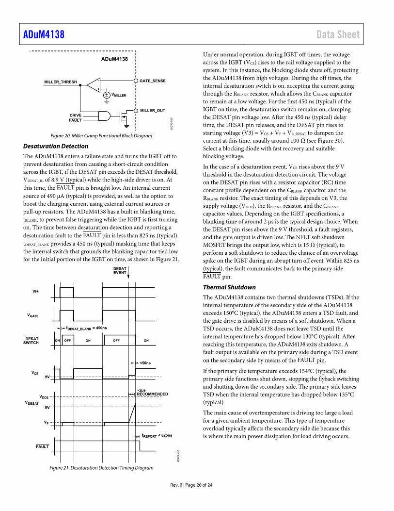
The ADuM4138 has an integrated Miller clamp control signal to reduce voltage spikes on the IGBT gate due to the Miller capacitance during shutoff of the IGBT. When the input gate signal calls for the IGBT to turn off (drive low), the external Miller clamp MOSFET signal is initially off. When the voltage on the GATE_SENSE pin crosses the 2 V (typical) internal voltage reference, as referenced to GND2, the Miller clamp latches on for the remainder of the off time of the IGBT, creating a second low impedance current path for the gate current to follow. The Miller clamp switch remains on until the input drive signal changes from low to high. Figure 19 shows an example waveform of this timing, and Figure 20 shows the functional block diagram of the Miller clamp.
VGATE_SENSE
VDD2
GND2
MILLERCLAMP
SWITCH
2V
VI+
ONOFF OFF
LATCH OFFLATCH ON 1603
6-01
2
Figure 19. Miller Clamp Example Waveform of Timing
ADuM4138 Data Sheet
Rev. 0 | Page 20 of 24
ADuM4138
GATE_SENSE
VMILLER
MILLER_OUT
MILLER_THRESH
DRIVEFAULT
1603
6-01
3
Figure 20. Miller Clamp Functional Block Diagram
Desaturation Detection
The ADuM4138 enters a failure state and turns the IGBT off to prevent desaturation from causing a short-circuit condition across the IGBT, if the DESAT pin exceeds the DESAT threshold, VDESAT_R, of 8.9 V (typical) while the high-side driver is on. At this time, the FAULT pin is brought low. An internal current source of 490 μA (typical) is provided, as well as the option to boost the charging current using external current sources or pull-up resistors. The ADuM4138 has a built in blanking time, tBLANK, to prevent false triggering while the IGBT is first turning on. The time between desaturation detection and reporting a desaturation fault to the FAULT pin is less than 825 ns (typical). tDESAT_BLANK provides a 450 ns (typical) masking time that keeps the internal switch that grounds the blanking capacitor tied low for the initial portion of the IGBT on time, as shown in Figure 21.
VDESAT
VDD2
VF
9V
FAULT
VCE
tREPORT < 825ns
9V
~2µsRECOMMENDED
<50ns
VGATE
DESATSWITCH
ONOFFON OFF
VI+
DESATEVENT
ON
tDESAT_BLANK = 450ns
1603
6-01
4
Figure 21. Desaturation Detection Timing Diagram
Under normal operation, during IGBT off times, the voltage across the IGBT (VCE) rises to the rail voltage supplied to the system. In this instance, the blocking diode shuts off, protecting the ADuM4138 from high voltages. During the off times, the internal desaturation switch is on, accepting the current going through the RBLANK resistor, which allows the CBLANK capacitor to remain at a low voltage. For the first 450 ns (typical) of the IGBT on time, the desaturation switch remains on, clamping the DESAT pin voltage low. After the 450 ns (typical) delay time, the DESAT pin releases, and the DESAT pin rises to starting voltage (V3) = VCE + VF + VR_DESAT to dampen the current at this time, usually around 100 Ω (see Figure 30). Select a blocking diode with fast recovery and suitable blocking voltage.
In the case of a desaturation event, VCE rises above the 9 V threshold in the desaturation detection circuit. The voltage on the DESAT pin rises with a resistor capacitor (RC) time constant profile dependent on the CBLANK capacitor and the RBLANK resistor. The exact timing of this depends on V3, the supply voltage (VDD2), the RBLANK resistor, and the CBLANK capacitor values. Depending on the IGBT specifications, a blanking time of around 2 μs is the typical design choice. When the DESAT pin rises above the 9 V threshold, a fault registers, and the gate output is driven low. The NFET soft shutdown MOSFET brings the output low, which is 15 Ω (typical), to perform a soft shutdown to reduce the chance of an overvoltage spike on the IGBT during an abrupt turn off event. Within 825 ns (typical), the fault communicates back to the primary side FAULT pin.
Thermal Shutdown
The ADuM4138 contains two thermal shutdowns (TSDs). If the internal temperature of the secondary side of the ADuM4138 exceeds 150°C (typical), the ADuM4138 enters a TSD fault, and the gate drive is disabled by means of a soft shutdown. When a TSD occurs, the ADuM4138 does not leave TSD until the internal temperature has dropped below 130°C (typical). After reaching this temperature, the ADuM4138 exits shutdown. A fault output is available on the primary side during a TSD event on the secondary side by means of the FAULT pin.
If the primary die temperature exceeds 154°C (typical), the primary side functions shut down, stopping the flyback switching and shutting down the secondary side. The primary side leaves TSD when the internal temperature has dropped below 135°C (typical).
The main cause of overtemperature is driving too large a load for a given ambient temperature. This type of temperature overload typically affects the secondary side die because this is where the main power dissipation for load driving occurs.

Data Sheet ADuM4138
Rev. 0 | Page 21 of 24
Isolated Temperature Sensor
The ADuM4138 allows simple isolated temperature detection. Using an internal current source to bias an external temperature sensing diode, the ADuM4138 encodes the forward-biased voltage of the diode into a PWM signal, which is passed across the isolation barrier from the secondary side to the primary side. The PWM signal operates at 10 kHz or 50 kHz (programmed in the EEPROM). A 10% (typical) PWM signal corresponds to a voltage of 2.45 V, and a 92% (typical) PWM signal corresponds to 1.55 V. Voltages between the minimum and maximum are approximately linear and monotonically interpolated. The ADuM4138 contains support for two remote temperature sensing diode assemblies, which can both cause overheating faults on the secondary side. Additionally, one temperature sensor readback is available for reading on the primary side through the isolated temperature reporting channel. The lower voltage (higher temperature) of the two temperature sensor pins, TS1 and TS2, reports on the TEMP_OUT pin. The gain and offset of the PWM temperature sensor can be set in the TEMP_OUT pin voltage mapping (see Figure 22).
1.0
0.9
0.8
0.7
0.6
DU
TY
CY
CL
E (
No
rmal
ized
)
0.5
0.4
0.3
0.2
0.1
00 0.5 1.0 1.5 2.0
TSx PIN VOLTAGE (V)
2.5 3.0 3.5
TS1TS2
1603
6-01
5
Figure 22. TEMP_OUT Duty Cycle vs. Lower TSx Pin Voltage
A low temperature operation mode is available if the voltage sensed on the TS1 pin is greater than 2.4 V (typical), the maximum gate voltage is set to the two-level plateau voltage of 11.90 V (typical), see Figure 23. Hysteresis allows continued low temperature operation until the TS1 pin voltage goes below 2.36 V (typical). Low temperature operation can be enabled or disabled in the EEPROM settings in the LOW_T_OP bit, Address 01, Bit 12. Basic operation is shown in Figure 23. During the two-level drive, the RDSON resistances of the turn on and turn off drivers increase to approximately 4 times the normal turn on and turn off resistances.
2.36V
GATE DRIVE LEVEL
2.4V
11.90V
VDD2
TS1 VOLTAGE 1603
6-01
6
Figure 23. Low Temperature Operation
ADuM4138
TS2
TS1
VOT
∆t = tdOT
OT_ERROR
VOC_OFF
SAWTOOTH
IT2
VLOW_TEMP
HYSTERESIS
LOW_T_OP
VT_OFFSET1
GAIN1
VT_OFFSET2
GAIN2TEMP_OUT_PWM
EPROM
GAIN1VT_OFFSET1GAIN2VT_OFFSET2
TEMP_OUT
V5
IT1
1603
6-01
7NOTES1. VLOW_TEMP IS THE LOW TEMPERATURE OPERATION COMPARATOR REFERENCE.2. VOT IS THE OVERTEMPERATURE ERROR COMPARATOR REFERENCE.
Figure 24. Remote Temperature Sensing Block Diagram

ADuM4138 Data Sheet
Rev. 0 | Page 22 of 24
POWER DISSIPATION When driving an IGBT gate, the driver must dissipate power. This power can lead to TSD if the following considerations are not made. The gate of an IGBT can be simulated roughly as a capacitive load. Due to Miller capacitance and other nonlinearities, it is common practice to take the stated input capacitance (CISS) of a given IGBT and multiply it by a factor of 5 to arrive at a conservative estimate to approximate the load being driven. With this value, the estimated total power dissipation (PDISS) in the system due to switching action is given by the following equation:
PDISS = CEST × (VDD2)2 × fS
where: CEST = CISS × 5. VDD2 is the voltage on the VDD2 pin.fS is the switching frequency of IGBT.
This power dissipation is shared between the internal on resistances of the internal gate driver switches and the external gate resistances, RGON and RGOFF. The ratio of the internal gate resistances to the total series resistance allows the calculation of losses seen within the ADuM4138 chip.
Take the power dissipation found inside the chip due to switching, adding the quiescent power losses, and multiplying it by the θJA gives the rise above ambient temperature that the ADuM4138 experiences.
PDISS_ADUM4138 = PDISS × 0.5(RDSON_P ÷ (RGON + RDSON_P) + (RDSON_N ÷ (RGOFF + RDSON_N)) + PQUIESCENT
where: PDISS_ADUM4138 is the power dissipation of the ADuM4138. RGON is the external series resistance in the on path. PGOFF is the external series resistance in the off path. PQUIESCENT is the quiescent power.
TADuM4138 = θJA × PDISS_ADuM4138 + TAMB
where: TADuM4138 is the junction temperature of the ADuM4138. TAMB is the ambient temperature.
For the ADuM4138 to remain within specification, TADuM4138 cannot exceed 150°C (typical). When TADuM4138 exceeds 150°C (typical), the ADuM4138 enters TSD.
INSULATION LIFETIME All insulation structures eventually break down when subjected to voltage stress over a sufficiently long period. The rate of insulation degradation is dependent on the characteristics of the voltage waveform applied across the insulation. In addition to the testing performed by the regulatory agencies, Analog Devices carries out an extensive set of evaluations to determine the lifetime of the insulation structure within the ADuM4138.
Analog Devices performs accelerated life testing using voltage levels higher than the rated continuous working voltage. Acceleration factors for several operating conditions are determined. These factors allow calculation of the time to failure at the actual working voltage.
The values shown Table 10 summarize the peak voltage for 20 years of service life for a bipolar ac operating condition, and the maximum CSA/VDE approved working voltages. In many cases, the approved working voltage is higher than the 20 year service life voltage. Operation at these high working voltages can lead to shortened insulation life in some cases.
The insulation lifetime of the ADuM4138 depends on the voltage waveform type imposed across the isolation barrier. The iCoupler insulation structure degrades at different rates depending on whether the waveform is bipolar ac, unipolar ac, or dc. Figure 25, Figure 26, and Figure 27 show these different isolation voltage waveforms.
A bipolar ac voltage environment is the worst case for the iCoupler products and is the 20 year operating lifetime that Analog Devices recommends for maximum working voltage (see Figure 25). In the case of unipolar ac or dc voltage, the stress on the insulation is significantly lower, which allows operation at higher working voltages while still achieving a 20 year service life. Treat any cross insulation voltage waveform that does not conform to Figure 26 or Figure 27 as a bipolar ac waveform, and limit its peak voltage to the 20 year lifetime voltage value listed in Table 10.
The voltage presented in Figure 26 is shown as sinusoidal for illustration purposes only. It is meant to represent any voltage waveform varying between 0 V and some limiting value. The limiting value can be positive or negative, but the voltage cannot cross 0 V.
0V
RATED PEAK VOLTAGE
1603
6-01
8
Figure 25. Bipolar AC Waveform
0V
RATED PEAK VOLTAGE
1603
6-01
9
Figure 26. Unipolar AC Waveform
0V
RATED PEAK VOLTAGE
1603
6-02
0
Figure 27. Unipolar DC Waveform
Data Sheet ADuM4138
Rev. 0 | Page 23 of 24
DC CORRECTNESS AND MAGNETIC FIELD IMMUNITY The ADuM4138 is resistant to external magnetic fields. The limitation on the ADuM4138 magnetic field immunity is set by the condition in which the induced voltage in the transformer receiving coil is sufficiently large to either falsely set or reset the decoder. The following analysis defines the conditions under which this can occur.
100
10
1
0.1
0.01
0.0011k 10k 100k 1M 10M 100M
MA
XIM
UM
AL
LO
WA
BL
E M
AG
NE
TIC
FL
UX
DE
NS
ITY
(kg
auss
)
MAGNETIC FIELD FREQUENCY (Hz) 1603
6-02
1
Figure 28. Maximum Allowable External Magnetic Flux Density
1k
100
10
1
0.1
0.011k 10k 100k 1M 10M 100M
MA
XIM
UM
AL
LO
WA
BL
E C
UR
RE
NT
(kA
)
MAGNETIC FIELD FREQUENCY (Hz)
DISTANCE = 1m
DISTANCE = 100mm
DISTANCE = 5mm
1603
6-02
2
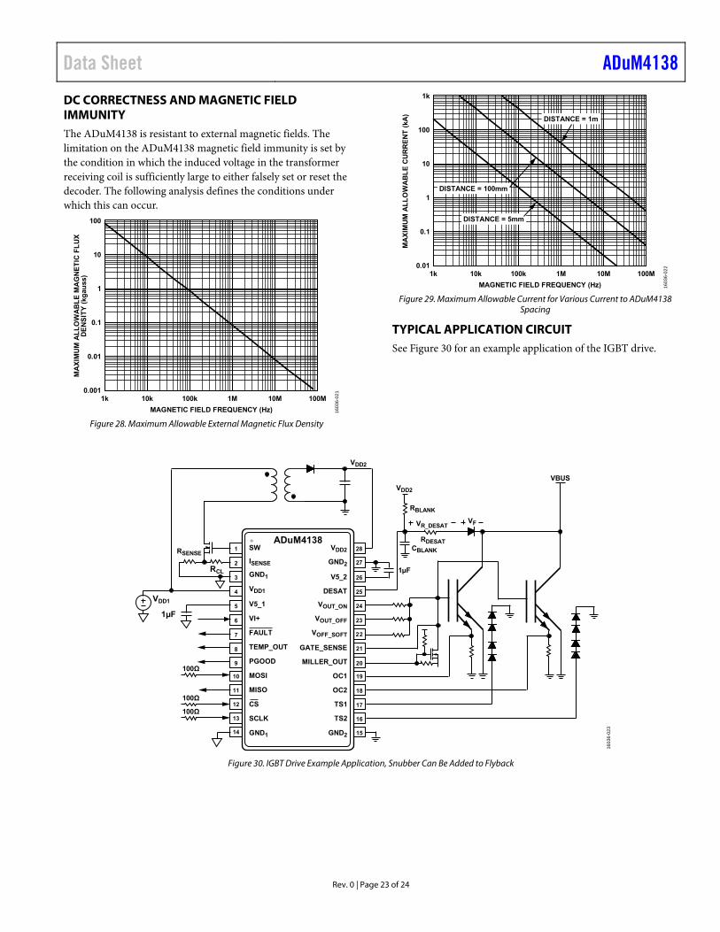
Figure 29. Maximum Allowable Current for Various Current to ADuM4138
Spacing
TYPICAL APPLICATION CIRCUIT See Figure 30 for an example application of the IGBT drive.
1
2
3
4
5
6
7
8
17
ADuM4138
9
16
VDD2
10
11
12
19
18
20
21
22
23
24
15
13
14
25
26
27
28
RDESAT
VFVR_DESAT
RBLANK
CBLANK
VDD1
VDD2
1µF
VBUS
1µFRCL
RSENSEVDD2
GND2
VOUT_ON
VOUT_OFF
V5_2
VOFF_SOFT
MILLER_OUT
DESAT
GATE_SENSE
OC1
OC2
GND2
TS1
TS2
SW
GND1
V5_1
VI+
CS
MOSI
ISENSE
SCLK
VDD1
PGOOD
FAULT
TEMP_OUT
GND1
MISO
1603
6-02
3
100Ω
100Ω
100Ω
Figure 30. IGBT Drive Example Application, Snubber Can Be Added to Flyback

ADuM4138 Data Sheet
Rev. 0 | Page 24 of 24
OUTLINE DIMENSIONS
28 15
141
SEATINGPLANE
0.250.10
0.400.25
0.65 BSC
1.40REF
COPLANARITY0.10
2.402.25
2.652.35
0.750.25
10.4510.15
7.607.40
10.5510.05
PK
G-0
0467
8
06-0
1-2
015
-A
× 45°
TOP VIEW
SIDE VIEW END VIEW
0.320.23
1.270.40
8°0°
0.25 BSC(GAUGE PLANE)
PIN 1INDICATOR
Figure 31. 28-Lead Standard Small Outline, Wide Body with Finer Pitch [SOIC_W_FP]
(RN-28-1) Dimensions shown in millimeters
ORDERING GUIDE
Model1, 2 Temperature Range Package Description Package Option
ADuM4138WBRNZ −40°C to +150°C 28-Lead Standard Small Outline, Wide Body with Finer Pitch [SOIC_W_FP] RN-28-1 ADuM4138WBRNZ-RL −40°C to +150°C 28-Lead Standard Small Outline, Wide Body, with Finer Pitch [SOIC_W_FP] RN-28-1 EVAL-ADuM4138EBZ Evaluation Board 1 Z = RoHS Compliant Part. 2 W = Qualified for Automotive Applications.
AUTOMOTIVE PRODUCTS The ADuM4138W models are available with controlled manufacturing to support the quality and reliability requirements of automotive applications. Note that these automotive models may have specifications that differ from the commercial models; therefore, designers should review the Specifications section of this data sheet carefully. Only the automotive grade products shown are available for use in automotive applications. Contact your local Analog Devices account representative for specific product ordering information and to obtain the specific Automotive Reliability reports for these models.
©2018 Analog Devices, Inc. All rights reserved. Trademarks and registered trademarks are the property of their respective owners. D16036-0-12/18(0)