Application-specific oxide-based and metal-dielectric thin ...
1SNOA946–April 2016Submit Documentation Feedback
Copyright © 2016, Texas Instruments Incorporated
High Voltage Half Bridge Design Guide for LMG3410 Smart GaN FET
Application ReportSNOA946–April 2016
High Voltage Half Bridge Design Guide for LMG3410Smart GaN FET
Eric Faraci and Jie Mao
ABSTRACTAs gallium nitride (GaN) power FETs become readily available for power designers to use, their promiseof performance improvement with higher efficiencies and greater power densities can begin to becomerealized. By having better material properties over silicon, loss elements such as on-state resistanceRds(on) and output capacitance Coss are smaller for an equal die area. These GaN power FET devices,such as the LMG3410, are typically offered in high electron mobility transistor (HEMT) structures, whichalong with maximizing the material property benefits eliminate the reverse recovery Qrr when the deviceoperates in third quadrant mode (conduction from source to drain). These benefits allow GaN power FETsto operate faster and at higher frequencies than previously capable. With typical slew rates around 30V/ns to 100 V/ns at operating voltages around 380 V to 480 V, printed circuit board (PCB) layoutoptimization is even more essential since parasitic inductances and capacitances from poor layouts candrastically reduce performance or even prevent operation. When pushed to their limits to maximize systemgains power GaN FETs provide the device can degrade and potentially overheat without a carefullydesigned thermal system to dissipate the generated heat. To prevent these problems from hamperingdesigns and limiting performance layout recommendations, peripheral component selection and thermalsystem design are discussed.
Contents1 Introduction ................................................................................................................... 22 Component Selection ....................................................................................................... 63 Thermal Design Considerations .......................................................................................... 104 Example PCB Layout ...................................................................................................... 155 Example Results ........................................................................................................... 186 References .................................................................................................................. 19
TrademarksAll trademarks are the property of their respective owners.
0 rtrace
hL l
W
P P|
lkdi
V Ldt
Introduction www.ti.com
2 SNOA946–April 2016Submit Documentation Feedback
Copyright © 2016, Texas Instruments Incorporated
High Voltage Half Bridge Design Guide for LMG3410 Smart GaN FET
1 IntroductionIn order to maximize the performance benefit of the LMG3410, a robust PCB layout is essential. Whilethere are design rules that help improve performance for one parameter, they also can cause anotherparameter to become worse. This requires an understanding of all the main design tradeoffs to create anoptimized layout. While following design recommendations for lower voltage GaN FETs are recommendedfor proper operation, the higher voltages seen by the LMG3410 requires special consideration to insureproper operation (see SNVA729).
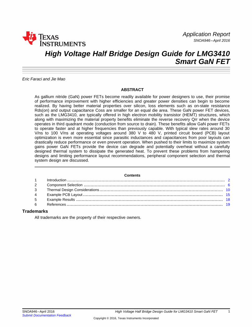
1.1 Parasitic InductanceBy having smaller gate capacitance, output capacitance and on state resistance, GaN FETs are able toswitch much faster with less loss. The LMG3410 has a user-controllable slew rate from 30 V/ns to 100V/ns. While this helps reduce the power loss during each switching transition, it also increases the voltageand current slew rates. As Equation 1 shows, by increasing the current slew rate the voltage inducedacross any parasitic inductor is increased, increasing voltage overshoot on the power device.
where• Llk is the parasitic inductance• di/dt is the change of current with respect to time• V is the induced voltage (1)
Since high slew rates are desired to minimize switching transitions and reduce loss, it is important to keepthe parasitic inductance as small as possible. One key current loop is the switching cell and bypasscapacitor. Figure 1 highlights this loop for a half bridge configuration, which includes the high side FET,low side FET and bypass capacitor.
Figure 1. Critical Power Stage Current Loop
Any closed current loop has an inductance, which can be approximated with Equation 2 (see InductanceFormulas for Circular and Square Coils).
where• μ0 is the permeability of free air (4π×10-7)• μr is the relative permeability (1 for FR-4)• h is the space between conductors• w is the width of the conductor• l is the length of the conductor• Ltrace is the parasitic inductance of the trace (2)

LegendOuter Metal
Inner Metal
Via
PCB Dielectric
LMG3410 LMG3410
BypassCapacitor
www.ti.com Introduction
3SNOA946–April 2016Submit Documentation Feedback
Copyright © 2016, Texas Instruments Incorporated
High Voltage Half Bridge Design Guide for LMG3410 Smart GaN FET
The parasitic inductance Ltrace can be minimized by reducing the space between traces h and length lwhile maximizing the width w. By placing all the components on the top layer of a PCB, and have thereturn path on the next layer of copper, the space between conductors h can be greatly reduced, creatingan optimal layout (see Understanding the Effect of PCB Layout on Circuit Performance in a High-Frequency Gallium-Nitride-Based Point of Load Converter).
Figure 2. Optimal Layout (Cross-Section View)
By reducing this inductance with an optimized layout, the voltage overshoots that increase stress andlosses are reduced, improving performance of the LMG3410.
1.2 Parasitic Capacitance
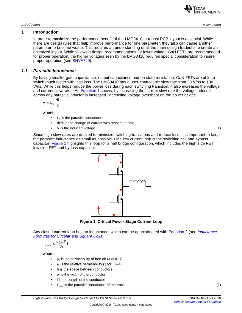
1.2.1 PCB LayoutTo properly layout PCBs that utilize GaN, multiple layer boards are required. Any time when a multilayerboard is designed, copper overlaps between key nets need to be minimized to prevent undesired parasiticcapacitors from being created and hurting performance. One key net that needs to be taken intoconsideration is the switch node, which is highlighted on Figure 3. Any capacitance from this node toground or input voltage leads to additional energy that is dissipated through the GaN FET during turn on,increasing switching loss. Layouts that minimize the parasitic inductance by with large ground returncurrent loop widths can have large parasitic switch node capacitance if not properly accounted for.
r0.0886 AC
h
H
Ground
Switch Node
Input Voltage
Ground
Source Pad
LegendMetal 1
Metal 2
Vias
Bypass Capacitors
Source Pad
Drain PadOverlap
Drain Pad
Introduction www.ti.com
4 SNOA946–April 2016Submit Documentation Feedback
Copyright © 2016, Texas Instruments Incorporated
High Voltage Half Bridge Design Guide for LMG3410 Smart GaN FET
Figure 3. Parasitic Capacitance Example
The parasitic capacitance from a PCB can be approximated with Equation 3 (see SLYP173).
where• h is the distance between copper layers in cm• A is the overlapping area in cm2
• εr is the relative permittivity (4.5 for FR-4)• C is the capacitance in pF (3)

TIM Heatsink
2cap SW OSS IN
1P f C V
2
www.ti.com Introduction
5SNOA946–April 2016Submit Documentation Feedback
Copyright © 2016, Texas Instruments Incorporated
High Voltage Half Bridge Design Guide for LMG3410 Smart GaN FET
For example, if a board that has 5 mils between the switch node and ground return and has an overlaparea of 0.64 cm2 (the area of the LMG3410), then the additional capacitance is 20 pF. The LMG3410output capacitance is only 90 pF under high Vds bias, which makes this capacitance a significant term thatincreases the total effective capacitance by 22%. This capacitance can increase the power loss dissipatedby the LMG3410 during turn on, and can be approximated with Equation 4 (see SLYY071).
where• fsw is the switching frequency• Coss is the output capacitance• VIN is the input switching voltage• Pcap is the power loss (4)
For example, at 140 kHz and 380 V, a capacitance of 20 pF will increase the loss dissipated by the activeswitched LMG3410 by 0.4 W. The capacitance of the ground-return path underneath the die attach pad(DAP) of the LMG3410 and the switch-node copper needs to be minimized, for example, by increasing thegap between the different PCB layers and reducing trace widths.
1.2.2 HeatsinkAnother source of parasitic capacitance is the heatsink. Typically conductive materials such as aluminumare used to sink heat away. If one heatsink is used to cool two LMG3410 devices in a half bridge, aninsulating thermal interface material (TIM) is required. The LMG3410 dissipates heat through the dieattached pad (DAP), which is also electrically connected to the source. In a half bridge configuration, thismeans the heatsink is capacitive coupled to the switch node and ground.
Figure 4. Parasitic Capacitance from Floating Heatsink Connection in Half Bridge Configuration
By sharing a heatsink in this configuration, a parasitic capacitance exists from switch node to ground. Ifthe heatsink is grounded, this parasitic capacitance is increased. This means that a large copper plane toallow for high thermal conductivity to the heatsink may not be optimal for parasitic capacitance. Highthermal conductivity and low parasitic capacitance should be traded off in system level to achieve optimalperformance. Sometimes, it could become necessary to slip top-side and bottom-side heatsinks andground differently. Thermal considerations are further discussed in the thermal section.
Introduction www.ti.com
6 SNOA946–April 2016Submit Documentation Feedback
Copyright © 2016, Texas Instruments Incorporated
High Voltage Half Bridge Design Guide for LMG3410 Smart GaN FET
1.3 InterferenceEven with the best design, the power stage switching still causes interference in the bias power and logicsignals. This coupling can disturb sensitive logic signals, especially around the gate drive. Poor layoutscan result in overshoots large enough to inadvertently turn on devices, creating damaging shoot throughevents, increase loss with unintended turn-off glitches or corrupting fault signals to trigger false events.This interference can be reduced by minimizing copper overlaps between nets that have large voltageswings, such as the switch node. Low pass RC filters on the input and fault signals are recommended tofilter out any undesired ringing.
2 Component SelectionThe performance of the LMG3410 is largely dependent on the components that it interfaces with. Tomaximize the performance and prevent unforeseen problems from interfering with operation, propercomponent such as capacitors, diodes, and integrated circuits need to be selected.
2.1 Decoupling/Bypass CapacitorTypically for high voltage systems, large bulk film or electrolytic capacitors are used to hold up the DCbus. While sufficient for low frequency operation, these capacitors do not perform well at the very highslew rates that the LMG3410 operates at due to their large size and series inductance. To compensate forthis, high quality surface mount capacitors are required to be placed in parallel. High quality ceramics withX7R or NP0/C0G dielectrics are recommended due to their low variation over temperature and voltage. Bybeing in surface mount packages the parasitic inductance is significantly reduced and much tighter currentloops can be achieved with the optimal layout discussed earlier, minimizing voltage overshoot duringswitching transitions.
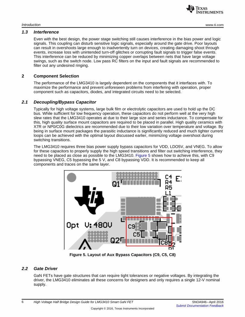
The LMG3410 requires three bias power supply bypass capacitors for VDD, LDO5V, and VNEG. To allowfor these capacitors to properly supply the high speed transitions and filter out switching interference, theyneed to be placed as close as possible to the LMG3410. Figure 5 shows how to achieve this, with C9bypassing VNEG, C5 bypassing the 5 V, and C8 bypassing VDD. It is recommended to keep allcomponents and traces on the same layer.
Figure 5. Layout of Aux Bypass Capacitors (C9, C5, C8)
2.2 Gate DriverGaN FETs have gate structures that can require tight tolerances or negative voltages. By integrating thedriver, the LMG3410 eliminates all these concerns for designers and only requires a single 12-V nominalsupply.

www.ti.com Component Selection
7SNOA946–April 2016Submit Documentation Feedback
Copyright © 2016, Texas Instruments Incorporated
High Voltage Half Bridge Design Guide for LMG3410 Smart GaN FET
2.3 High Side Level and Power ShiftingTo supply logic and power to properly drive a high side device, level shifting needs to be providedexternally to the LMG3410. Design considerations need to be taken into consideration when selectingthem, or else they will introduce adverse behaviors that will limit or prevent operation.
2.3.1 High Side Level ShiftingTo convert logic signals from the controller to a high side device, a logic level shifter must be used. Digitalisolators are recommended due to their low propagation delay. Isolators with high common mode transientimmunity (CMTI) are required, since many standard isolators are only rated to 50 V/ns or less. Edgetriggered isolators are not recommended since the interference generated by the high slew rates of thepower stage can cause false triggers, causing circuit malfunction. On/off keyed isolators, such as theTexas Instruments ISO78xxF series isolators, are recommended since simple RC low pass filters on theinputs can eliminate any false pulses caused by high slew rates.
2.3.2 High Side Isolated PowerThe recommended way to power the LMG3410 when it is configured as a high side device is with anisolated power supply, such as the Texas Instruments DCP010512BP-U. A power supply with lowcapacitance from the input to output should be used since this directly leads to additional capacitance atthe switch node, increasing loss and creating a path for the switching transition to introduce interference inthe logic signals.
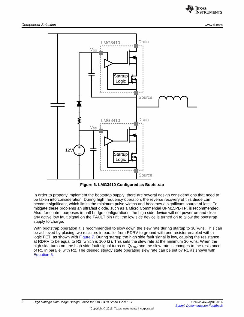
2.3.3 High Side Bootstrap PowerWhile a transformer-isolated power supply is recommended to power the LMG3410, a bootstrap supplycan be used with the following recommendations. The LMG3410 can be configured to operate with abootstrap supply as Figure 6 shows.
12V
LMG3410 Drain
Source
Startup Logic
VDD
LMG3410 Drain
Source
Startup Logic
VDD
Component Selection www.ti.com
8 SNOA946–April 2016Submit Documentation Feedback
Copyright © 2016, Texas Instruments Incorporated
High Voltage Half Bridge Design Guide for LMG3410 Smart GaN FET
Figure 6. LMG3410 Configured as Bootstrap
In order to properly implement the bootstrap supply, there are several design considerations that need tobe taken into consideration. During high frequency operation, the reverse recovery of this diode canbecome significant, which limits the minimum pulse widths and becomes a significant source of loss. Tomitigate these problems an ultrafast diode, such as a Micro Commercial UFM15PL-TP, is recommended.Also, for control purposes in half bridge configurations, the high side device will not power on and clearany active low fault signal on the FAULT pin until the low side device is turned on to allow the bootstrapsupply to charge.
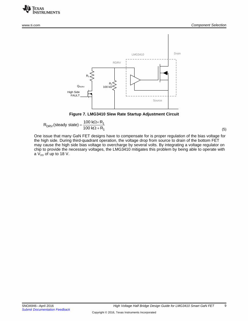
With bootstrap operation it is recommended to slow down the slew rate during startup to 30 V/ns. This canbe achieved by placing two resistors in parallel from RDRV to ground with one resistor enabled with alogic FET, as shown with Figure 7. During startup the high side fault signal is low, causing the resistanceat RDRV to be equal to R2, which is 100 kΩ. This sets the slew rate at the minimum 30 V/ns. When thehigh side turns on, the high side fault signal turns on QRDRV and the slew rate is changes to the resistanceof R1 in parallel with R2. The desired steady state operating slew rate can be set by R1 as shown withEquation 5.
1DRV
1
100 k RR (steady state)
100 k R
:u
: �
LMG3410
RDRV
Drain
Source
QRDRV
R2
100 k �
R1
High SideFAULT
www.ti.com Component Selection
9SNOA946–April 2016Submit Documentation Feedback
Copyright © 2016, Texas Instruments Incorporated
High Voltage Half Bridge Design Guide for LMG3410 Smart GaN FET
Figure 7. LMG3410 Slew Rate Startup Adjustment Circuit
(5)
One issue that many GaN FET designs have to compensate for is proper regulation of the bias voltage forthe high side. During third-quadrant operation, the voltage drop from source to drain of the bottom FETmay cause the high side bias voltage to overcharge by several volts. By integrating a voltage regulator onchip to provide the necessary voltages, the LMG3410 mitigates this problem by being able to operate witha VDD of up to 18 V.
Thermal pad
LMG3410
Top copper layer
Middle copper
Middle copper
Bottom copper
FR4
FR4
FR4
PCB
Thermal interface material (TIM)
Heatsink
Thermal vias
Tj
Tambient
Tcase
Rθ, jc bottom
Rθ, PCB
Rθ, TIM
Rθ, heatsink
Rθ, jc top
Thermal Design Considerations www.ti.com
10 SNOA946–April 2016Submit Documentation Feedback
Copyright © 2016, Texas Instruments Incorporated
High Voltage Half Bridge Design Guide for LMG3410 Smart GaN FET
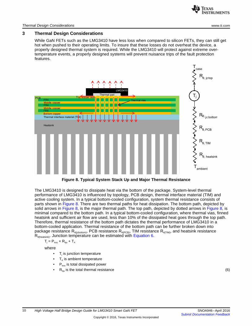
3 Thermal Design ConsiderationsWhile GaN FETs such as the LMG3410 have less loss when compared to silicon FETs, they can still gethot when pushed to their operating limits. To insure that these losses do not overheat the device, aproperly designed thermal system is required. While the LMG3410 will protect against extreme over-temperature events, a properly designed systems will prevent nuisance trips of the fault protectionfeatures.
Figure 8. Typical System Stack Up and Major Thermal Resistance
The LMG3410 is designed to dissipate heat via the bottom of the package. System-level thermalperformance of LMG3410 is influenced by topology, PCB design, thermal interface material (TIM) andactive cooling system. In a typical bottom-cooled configuration, system thermal resistance consists ofparts shown in Figure 8. There are two thermal paths for heat dissipation. The bottom path, depicted bysolid arrows in Figure 8, is the major thermal path. The top path, depicted by dotted arrows in Figure 8, isminimal compared to the bottom path. In a typical bottom-cooled configuration, where thermal vias, finnedheatsink and sufficient air flow are used, less than 10% of the dissipated heat goes through the top path.Therefore, thermal resistance of the bottom path dictates the thermal performance of LMG3410 in abottom-cooled application. Thermal resistance of the bottom path can be further broken down intopackage resistance Rθ(jcbottom), PCB resistance Rθ(PCB), TIM resistance Rθ(TIM), and heatsink resistanceRθ(heatsink). Junction temperature can be estimated with Equation 6.
Tj = Ploss × Rθja + TA
where• Tj is junction temperature• TA is ambient temperature• Ploss is total dissipated power• Rθja is the total thermal resistance (6)

tR
KA
www.ti.com Thermal Design Considerations
11SNOA946–April 2016Submit Documentation Feedback
Copyright © 2016, Texas Instruments Incorporated
High Voltage Half Bridge Design Guide for LMG3410 Smart GaN FET
Rθja can be approximated with Equation 7:Rθja = Rθjc(bottom) + Rθ(PCB) + Rθ(TIM) + Rθ(heatsink)
where• Rθjc(bottom) is thermal resistance between junction of the die and package DAP• Rθ(PCB) is thermal resistance of the PCB• Rθ(TIM) is the thermal resistance of the TIM• Rθ(heatsink) is the thermal resistance of the heatsink (7)
Since Tj is a constant set by GaN material, reducing Rθja increases the power output of LMG3410 and alsoallows LMG3410 to operate at higher ambient temperature. Thermal optimization can be achieved byreducing Rθjc(bottom), Rθ(PCB), Rθ(TIM), and Rθ(heatsink) (see SPRABI3). Rθjc(bottom) is an intrinsic property ofLMG3410, which has been optimized by package design and material selection. The following discussionwill focus on thermal optimization of LMG3410 via PCB design, TIM selection and heatsink selection.
3.1 PCB Thermal Optimization
3.1.1 Top Copper LayerJust like electric resistance, thermal resistance is not an intrinsic material property. It is a function ofmaterial thermal conductivity and material dimensions, in a simple one-dimensional case:
where• t is material thickness• A is material area• K is material thermal conductivity (8)
When the heat source area is smaller than the heat drain area, thermal conduction takes a 3-dimensionalform and spreading resistance will come into play (see Spreading Resistance in Cylindrical SemiconductorDevices). The top surface of the copper layer can be viewed as the heat source, which is defined by thepackage thermal pad, and the bottom surface can be viewed as the heat drain. As the copper layer sizeincreases, due to heat spreading, the effective thermal resistance in the vertical direction decreases andreaches saturation beyond a certain point, which is determined by the copper thickness. In general, it isbeneficial to have a larger and thicker top copper layer. Since FR4 material in the PCB is a much poorerthermal conductor, only very limited heat spreading is expected in it. Heat spreading in top copper layerdetermines the heat conduction area through the FR4. As Equation 8 shows, increasing the area reducesthe thermal resistance. Therefore, the overall thermal resistance of the PCB is reduced when a larger topcopper layer is used. When other design constraints, electrical performance, cost, board dimensions, andso forth are satisfied, a larger top copper layer is preferred for thermal optimization.
Before plating
After plating
Top copper layer
Middle copper layer
Middle copper layer
Bottom copper layer
ViaV
iapla
ting
Via
pla
ting
IsolationFR4
FR4
FR4
Thermal Design Considerations www.ti.com
12 SNOA946–April 2016Submit Documentation Feedback
Copyright © 2016, Texas Instruments Incorporated
High Voltage Half Bridge Design Guide for LMG3410 Smart GaN FET
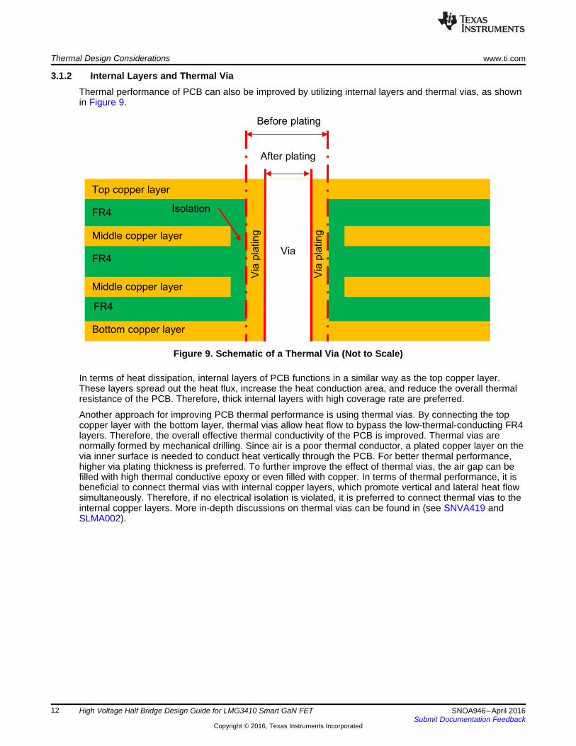
3.1.2 Internal Layers and Thermal ViaThermal performance of PCB can also be improved by utilizing internal layers and thermal vias, as shownin Figure 9.
Figure 9. Schematic of a Thermal Via (Not to Scale)
In terms of heat dissipation, internal layers of PCB functions in a similar way as the top copper layer.These layers spread out the heat flux, increase the heat conduction area, and reduce the overall thermalresistance of the PCB. Therefore, thick internal layers with high coverage rate are preferred.
Another approach for improving PCB thermal performance is using thermal vias. By connecting the topcopper layer with the bottom layer, thermal vias allow heat flow to bypass the low-thermal-conducting FR4layers. Therefore, the overall effective thermal conductivity of the PCB is improved. Thermal vias arenormally formed by mechanical drilling. Since air is a poor thermal conductor, a plated copper layer on thevia inner surface is needed to conduct heat vertically through the PCB. For better thermal performance,higher via plating thickness is preferred. To further improve the effect of thermal vias, the air gap can befilled with high thermal conductive epoxy or even filled with copper. In terms of thermal performance, it isbeneficial to connect thermal vias with internal copper layers, which promote vertical and lateral heat flowsimultaneously. Therefore, if no electrical isolation is violated, it is preferred to connect thermal vias to theinternal copper layers. More in-depth discussions on thermal vias can be found in (see SNVA419 andSLMA002).
www.ti.com Thermal Design Considerations
13SNOA946–April 2016Submit Documentation Feedback
Copyright © 2016, Texas Instruments Incorporated
High Voltage Half Bridge Design Guide for LMG3410 Smart GaN FET
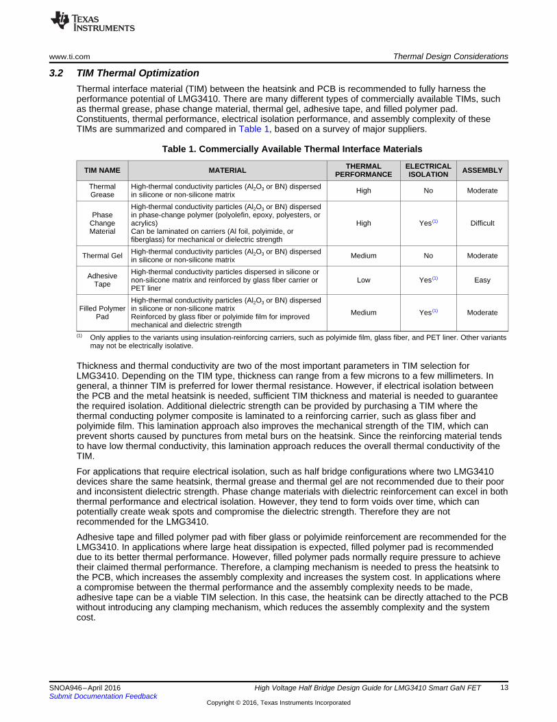
3.2 TIM Thermal OptimizationThermal interface material (TIM) between the heatsink and PCB is recommended to fully harness theperformance potential of LMG3410. There are many different types of commercially available TIMs, suchas thermal grease, phase change material, thermal gel, adhesive tape, and filled polymer pad.Constituents, thermal performance, electrical isolation performance, and assembly complexity of theseTIMs are summarized and compared in Table 1, based on a survey of major suppliers.
(1) Only applies to the variants using insulation-reinforcing carriers, such as polyimide film, glass fiber, and PET liner. Other variantsmay not be electrically isolative.
Table 1. Commercially Available Thermal Interface Materials
TIM NAME MATERIAL THERMALPERFORMANCE
ELECTRICALISOLATION ASSEMBLY
ThermalGrease
High-thermal conductivity particles (Al2O3 or BN) dispersedin silicone or non-silicone matrix High No Moderate
PhaseChangeMaterial
High-thermal conductivity particles (Al2O3 or BN) dispersedin phase-change polymer (polyolefin, epoxy, polyesters, oracrylics)Can be laminated on carriers (Al foil, polyimide, orfiberglass) for mechanical or dielectric strength
High Yes (1) Difficult
Thermal Gel High-thermal conductivity particles (Al2O3 or BN) dispersedin silicone or non-silicone matrix Medium No Moderate
AdhesiveTape
High-thermal conductivity particles dispersed in silicone ornon-silicone matrix and reinforced by glass fiber carrier orPET liner
Low Yes (1) Easy
Filled PolymerPad
High-thermal conductivity particles (Al2O3 or BN) dispersedin silicone or non-silicone matrixReinforced by glass fiber or polyimide film for improvedmechanical and dielectric strength
Medium Yes (1) Moderate
Thickness and thermal conductivity are two of the most important parameters in TIM selection forLMG3410. Depending on the TIM type, thickness can range from a few microns to a few millimeters. Ingeneral, a thinner TIM is preferred for lower thermal resistance. However, if electrical isolation betweenthe PCB and the metal heatsink is needed, sufficient TIM thickness and material is needed to guaranteethe required isolation. Additional dielectric strength can be provided by purchasing a TIM where thethermal conducting polymer composite is laminated to a reinforcing carrier, such as glass fiber andpolyimide film. This lamination approach also improves the mechanical strength of the TIM, which canprevent shorts caused by punctures from metal burs on the heatsink. Since the reinforcing material tendsto have low thermal conductivity, this lamination approach reduces the overall thermal conductivity of theTIM.
For applications that require electrical isolation, such as half bridge configurations where two LMG3410devices share the same heatsink, thermal grease and thermal gel are not recommended due to their poorand inconsistent dielectric strength. Phase change materials with dielectric reinforcement can excel in boththermal performance and electrical isolation. However, they tend to form voids over time, which canpotentially create weak spots and compromise the dielectric strength. Therefore they are notrecommended for the LMG3410.
Adhesive tape and filled polymer pad with fiber glass or polyimide reinforcement are recommended for theLMG3410. In applications where large heat dissipation is expected, filled polymer pad is recommendeddue to its better thermal performance. However, filled polymer pads normally require pressure to achievetheir claimed thermal performance. Therefore, a clamping mechanism is needed to press the heatsink tothe PCB, which increases the assembly complexity and increases the system cost. In applications wherea compromise between the thermal performance and the assembly complexity needs to be made,adhesive tape can be a viable TIM selection. In this case, the heatsink can be directly attached to the PCBwithout introducing any clamping mechanism, which reduces the assembly complexity and the systemcost.

Base plate
Fin
Thermal Design Considerations www.ti.com
14 SNOA946–April 2016Submit Documentation Feedback
Copyright © 2016, Texas Instruments Incorporated
High Voltage Half Bridge Design Guide for LMG3410 Smart GaN FET
3.3 Heatsink SelectionTo improve the thermal dissipation of the LMG3410, a heatsink is recommended. By connecting aheatsink, the thermal resistance can be reduced since the heat dissipation to the surrounding air is greatlyimproved.
Figure 10. Schematic of a Heatsink
Heatsinks are made out of materials with high thermal conductivity, such as aluminum and copper. Asshown in Figure 10, a typical heatsink consists of a base plate and a series of fin plates. To insure theheatsink conducts heat well a large copper pad connected to the DAP of the LMG3410 needs to beattached to the base plate. It is important to insure that the pad does not become too large though, sinceheatsinks are often times made out of electrically conductive materials and can create undesired parasiticcapacitance that can hurt performance. By having fins the surface area is increased, improving the abilityto dissipate heat into the surrounding air. The amount of heat that a heatsink can dissipate is quantified byits thermal impedance Rθ(heatsink), which is typically specified in °C/W and ideally is as low as possible. Toinsure that this resistance is as small as possible active cooling, which involves blowing air across the finswith a fan, is recommended for higher power applications. Typical heatsink data sheets include Rθ(heatsink)and airflow recommendations. It is recommended to select a heatsink by calculating the required Rθ(heatsink)with Equation 6 and Equation 7, then selecting one with an equal or lower resistance. Excessively largeoversized designs are not recommended since they unnecessarily increase cost and increase parasiticcapacitance impact (see How to Select a Heatsink).
1uFC16
0.01µFC2
0.01µFC3
0.01µFC4
0.01µF1206630V
C5
0.1uFC20
5V
VS
W
68pFC21
68pFC18
AGND
L322µH
VCC11
GND12
INA3
INB4
OUTC5
NC6
EN17
GND18
GND29
EN210
NC11
INC12
OUTB13
OUTA14
GND215
VCC216
U4ISO7831DWR
1
23
Q1
100kR10
68.1kR9
0.22µFC17
1uFC22
PGND
100µFC1
0.47µFC15
0.1µF
630V
C130.1µF
630V
C14
PGND
PFC_INPUT
HV_BUS
220µH
L2
PGND
1uFC19
AGND
DRAIN1
DRAIN2
DRAIN3
DRAIN4
DRAIN5
DRAIN6
DRAIN7
DRAIN8
DRAIN9
DRAIN10
DRAIN11
SOURCE12
SOURCE13
SOURCE14
SOURCE15
NC17
SOURCE16
SOURCE18
SOURCE19
SOURCE20
SOURCE21
SOURCE22
SOURCE23
GND24
LDO5V25
VNEG26
VDD27
BBSW28
LPM29
RDRV30
IN31
FAULT32
PAD33
U3
LMG3410RWH
DRAIN1
DRAIN2
DRAIN3
DRAIN4
DRAIN5
DRAIN6
DRAIN7
DRAIN8
DRAIN9
DRAIN10
DRAIN11
SOURCE12
SOURCE13
SOURCE14
SOURCE15
NC17
SOURCE16
SOURCE18
SOURCE19
SOURCE20
SOURCE21
SOURCE22
SOURCE23
GND24
LDO5V25
VNEG26
VDD27
BBSW28
LPM29
RDRV30
IN31
FAULT32
PAD33
U1
LMG3410RWH
10
R8
20R5
10
R7
1uFC6
0.1uFC10
5V
68pFC11
68pFC8
AGND
L122µH
VCC11
GND12
INA3
INB4
OUTC5
NC6
EN17
GND18
GND29
EN210
NC11
INC12
OUTB13
OUTA14
GND215
VCC216
U2ISO7831DWR
0.22µFC7
1uFC12
1uFC9
AGND
10
R3
10
R2
39kR4
D1UFM15PL-TP
PWM_H
PWM_L
FAULT_H
FAULT_L
10kR6
12V
10.0
R11
10kR1
www.ti.com Example PCB Layout
15SNOA946–April 2016Submit Documentation Feedback
Copyright © 2016, Texas Instruments Incorporated
High Voltage Half Bridge Design Guide for LMG3410 Smart GaN FET
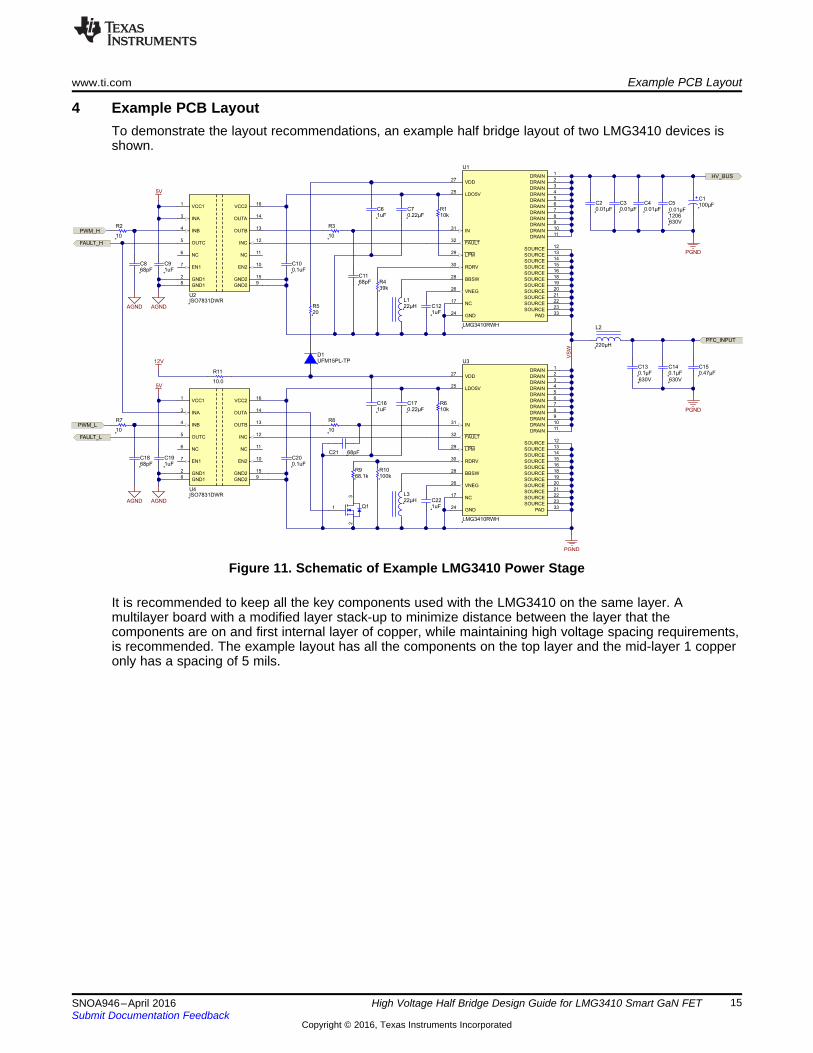
4 Example PCB LayoutTo demonstrate the layout recommendations, an example half bridge layout of two LMG3410 devices isshown.
Figure 11. Schematic of Example LMG3410 Power Stage
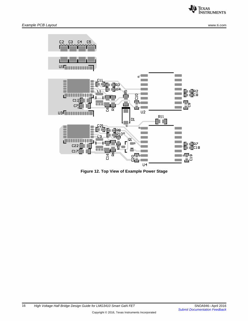
It is recommended to keep all the key components used with the LMG3410 on the same layer. Amultilayer board with a modified layer stack-up to minimize distance between the layer that thecomponents are on and first internal layer of copper, while maintaining high voltage spacing requirements,is recommended. The example layout has all the components on the top layer and the mid-layer 1 copperonly has a spacing of 5 mils.
Example PCB Layout www.ti.com
16 SNOA946–April 2016Submit Documentation Feedback
Copyright © 2016, Texas Instruments Incorporated
High Voltage Half Bridge Design Guide for LMG3410 Smart GaN FET
Figure 12. Top View of Example Power Stage
www.ti.com Example PCB Layout
17SNOA946–April 2016Submit Documentation Feedback
Copyright © 2016, Texas Instruments Incorporated
High Voltage Half Bridge Design Guide for LMG3410 Smart GaN FET
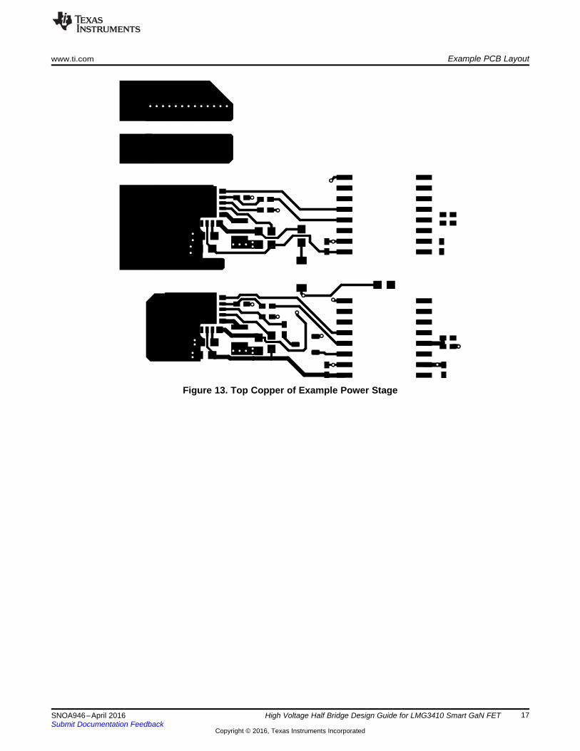
Figure 13. Top Copper of Example Power Stage
Example Results www.ti.com
18 SNOA946–April 2016Submit Documentation Feedback
Copyright © 2016, Texas Instruments Incorporated
High Voltage Half Bridge Design Guide for LMG3410 Smart GaN FET
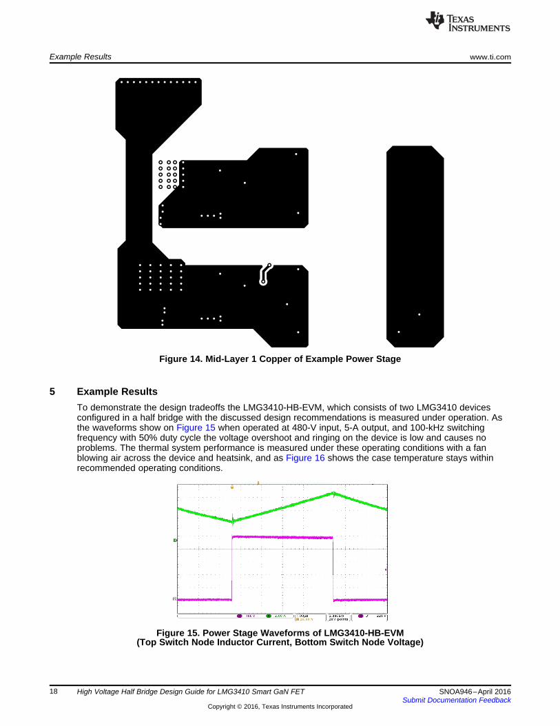
Figure 14. Mid-Layer 1 Copper of Example Power Stage
5 Example ResultsTo demonstrate the design tradeoffs the LMG3410-HB-EVM, which consists of two LMG3410 devicesconfigured in a half bridge with the discussed design recommendations is measured under operation. Asthe waveforms show on Figure 15 when operated at 480-V input, 5-A output, and 100-kHz switchingfrequency with 50% duty cycle the voltage overshoot and ringing on the device is low and causes noproblems. The thermal system performance is measured under these operating conditions with a fanblowing air across the device and heatsink, and as Figure 16 shows the case temperature stays withinrecommended operating conditions.
Figure 15. Power Stage Waveforms of LMG3410-HB-EVM(Top Switch Node Inductor Current, Bottom Switch Node Voltage)

www.ti.com References
19SNOA946–April 2016Submit Documentation Feedback
Copyright © 2016, Texas Instruments Incorporated
High Voltage Half Bridge Design Guide for LMG3410 Smart GaN FET
Figure 16. Thermal Measurement of LMG3410-HB-EVM
6 References1. Layout Guidelines for LMG5200 ~ 80-V, 10-A, GaN Power Stage Module, SNVA7292. Wheeler, H.A., "Inductance formulas for circular and square coils," in Proceedings of the IEEE , vol.70,
no.12, pp.1449-1450, Dec. 1982 doi: 10.1109/PROC.1982.12504URL: http://ieeexplore.ieee.org/stamp/stamp.jsp?tp=&arnumber=1456772&isnumber=31320
3. Reusch, D.; Strydom, J., "Understanding the Effect of PCB Layout on Circuit Performance in a High-Frequency Gallium-Nitride-Based Point of Load Converter," in Power Electronics, IEEE Transactionson , vol.29, no.4, pp.2008-2015, April 2014 doi: 10.1109/TPEL.2013.2266103URL: http://ieeexplore.ieee.org/stamp/stamp.jsp?tp=&arnumber=6531683&isnumber=6632912
4. High Speed Analog Design and Application Seminar, SLYP1735. GaN Power Module Performance Advantage in DC/DC Converters, SLYY0716. Thermal Design Guide for KeyStone Devices, SPRABI37. D.P. Kennedy, "Spreading Resistance in Cylindrical Semiconductor Devices" in J. Appl. Phys. 31, 1490
(1960);URL:http://dx.doi.org/10.1063/1.1735869
8. AN-2020 Thermal Design By Insight, Not Hindsight, SNVA4199. PowerPAD™ Thermally Enhanced Package, SLMA00210. "How to Select a Heatsink"
URL: http://www.aavid.com/sites/default/files/technical/papers/how-to-select-heatsink.pdf

IMPORTANT NOTICE FOR TI DESIGN INFORMATION AND RESOURCES
Texas Instruments Incorporated (‘TI”) technical, application or other design advice, services or information, including, but not limited to,reference designs and materials relating to evaluation modules, (collectively, “TI Resources”) are intended to assist designers who aredeveloping applications that incorporate TI products; by downloading, accessing or using any particular TI Resource in any way, you(individually or, if you are acting on behalf of a company, your company) agree to use it solely for this purpose and subject to the terms ofthis Notice.TI’s provision of TI Resources does not expand or otherwise alter TI’s applicable published warranties or warranty disclaimers for TIproducts, and no additional obligations or liabilities arise from TI providing such TI Resources. TI reserves the right to make corrections,enhancements, improvements and other changes to its TI Resources.You understand and agree that you remain responsible for using your independent analysis, evaluation and judgment in designing yourapplications and that you have full and exclusive responsibility to assure the safety of your applications and compliance of your applications(and of all TI products used in or for your applications) with all applicable regulations, laws and other applicable requirements. Yourepresent that, with respect to your applications, you have all the necessary expertise to create and implement safeguards that (1)anticipate dangerous consequences of failures, (2) monitor failures and their consequences, and (3) lessen the likelihood of failures thatmight cause harm and take appropriate actions. You agree that prior to using or distributing any applications that include TI products, youwill thoroughly test such applications and the functionality of such TI products as used in such applications. TI has not conducted anytesting other than that specifically described in the published documentation for a particular TI Resource.You are authorized to use, copy and modify any individual TI Resource only in connection with the development of applications that includethe TI product(s) identified in such TI Resource. NO OTHER LICENSE, EXPRESS OR IMPLIED, BY ESTOPPEL OR OTHERWISE TOANY OTHER TI INTELLECTUAL PROPERTY RIGHT, AND NO LICENSE TO ANY TECHNOLOGY OR INTELLECTUAL PROPERTYRIGHT OF TI OR ANY THIRD PARTY IS GRANTED HEREIN, including but not limited to any patent right, copyright, mask work right, orother intellectual property right relating to any combination, machine, or process in which TI products or services are used. Informationregarding or referencing third-party products or services does not constitute a license to use such products or services, or a warranty orendorsement thereof. Use of TI Resources may require a license from a third party under the patents or other intellectual property of thethird party, or a license from TI under the patents or other intellectual property of TI.TI RESOURCES ARE PROVIDED “AS IS” AND WITH ALL FAULTS. TI DISCLAIMS ALL OTHER WARRANTIES ORREPRESENTATIONS, EXPRESS OR IMPLIED, REGARDING TI RESOURCES OR USE THEREOF, INCLUDING BUT NOT LIMITED TOACCURACY OR COMPLETENESS, TITLE, ANY EPIDEMIC FAILURE WARRANTY AND ANY IMPLIED WARRANTIES OFMERCHANTABILITY, FITNESS FOR A PARTICULAR PURPOSE, AND NON-INFRINGEMENT OF ANY THIRD PARTY INTELLECTUALPROPERTY RIGHTS.TI SHALL NOT BE LIABLE FOR AND SHALL NOT DEFEND OR INDEMNIFY YOU AGAINST ANY CLAIM, INCLUDING BUT NOTLIMITED TO ANY INFRINGEMENT CLAIM THAT RELATES TO OR IS BASED ON ANY COMBINATION OF PRODUCTS EVEN IFDESCRIBED IN TI RESOURCES OR OTHERWISE. IN NO EVENT SHALL TI BE LIABLE FOR ANY ACTUAL, DIRECT, SPECIAL,COLLATERAL, INDIRECT, PUNITIVE, INCIDENTAL, CONSEQUENTIAL OR EXEMPLARY DAMAGES IN CONNECTION WITH ORARISING OUT OF TI RESOURCES OR USE THEREOF, AND REGARDLESS OF WHETHER TI HAS BEEN ADVISED OF THEPOSSIBILITY OF SUCH DAMAGES.You agree to fully indemnify TI and its representatives against any damages, costs, losses, and/or liabilities arising out of your non-compliance with the terms and provisions of this Notice.This Notice applies to TI Resources. Additional terms apply to the use and purchase of certain types of materials, TI products and services.These include; without limitation, TI’s standard terms for semiconductor products http://www.ti.com/sc/docs/stdterms.htm), evaluationmodules, and samples (http://www.ti.com/sc/docs/sampterms.htm).
Mailing Address: Texas Instruments, Post Office Box 655303, Dallas, Texas 75265Copyright © 2018, Texas Instruments Incorporated