High Stability Switching Mode Power Converters for …€¦ · · 2013-07-28A block diagram of...
3
HIGH STABILITY SWITCHING MODE POWER CONVERTERS FOR MAGNET LOADS Oscar Calvo, Coles Sibley and Tomas Russ Massachusetts Institute of Technology Bates Accelerator Center PO Box 846, Middleton, MA 01949 ABSTRACT The availability of general purpose switching mode power i es in the KW range has prompted the poss i bi l i ty of uS1ng them for powering optical elements in linear accelerators. They are, however, not designed specifi' cally to be operated as high stabi l ity current sources into inductive loads. We have modi f i ed and condi t i oned conmerc i a l off the shelf switching mode power supplies for use in' powering multipole magnets. Temperature stability in the constant current mode has been upgraded to 15 ppm/C. Other stability parameters have been similarly improved. We modeled power supply operation using the program Spice, and verified its results experimentally. An analog controller was designed to compensate for instabilities in the feedback loop. This circuit was incorporated into a Bi tbus power suppl y controller wh i ch is used as interface to the control system. Analysis of shielding techniques and tests results for a 2.5 KW power supply are provided. Introduction The South Hall Ring (SHR) under construction at the MIT Bates linear Acce l erator center wi II provi de high duty factor (CW) electron beams and an internal target capability for nuclear research. This project is the culmination of Bates developments over the last decade aimed at providing coincidence capability throughout the important energy range up to 1 GeV. Proper operation of the proposed pulse strecher ring places stringent criteria on the operation of all magnetic elements such as dipoles, quadrupoles, sextupoles, etc. A large number of power supplies, with power capabilities ranging up to 10 kW and stabilities better than 15 ppm full scale, are needed to power up all the multipole magnets. o • Cuslom ( 2 ppm) 6.3 Pow er (KII) 8.25 UOH Ihe shelf (200 - 500 + Cuslom (50 ppm) ppm) Figure 1. Power supply costs (with controller) 10 These requirements are normally satisfied with custom designed power supplies. However, in the Pulse Strecher, large nlnber of these suppl i es are needed and cost factors rule out this approach (figure 1). The well known advantages of swi tched mode power sup- plies, such as high efficiency, low weight and cost, make them very attractive for medium and high power levels. This popularity resulted in availability of off the shelf products at very reasonable prices. However, they are not to work as current controlled power suppl1es. They are usually built to operate in voltage controlled mode and powering resistive loads. The solution adopted here was to analyze the perform- ance of various conmercial power supplies and modify them to suit our needs. The internal controller was upgraded to enhance performance and stabi l ity with inductive loads. The current shunt was replaced by an external one with low temperature dri ft characteri st i cs. In addi ti on, a di gi ta l interface was provided for remote operation from a personal computer. Operation After a prel iminary selection of different vendors we opted for the EMS 40-60-2 power supply. This particular unit del ivers 2.5 kW but its circuitry is very simi lar for all the models ranging from one to five kilowatts. The suppl y operates in current and vol tage modes and is sui ted for resistive loads. It exhibits a long term stability of 500 ppm with a temperature coefficient of 300 ppm in current mode. It regulates within a 0.1 % with load or input voltage changes and has a ripple of 30 mV at 40 VI 60 Amps. A block diagram of the switched mode power converter is shown in figure 2. Figure 2. SMPS block diagram Proceedings of the Linear Accelerator Conference 1990, Albuquerque, New Mexico, USA 493
Transcript of High Stability Switching Mode Power Converters for …€¦ · · 2013-07-28A block diagram of...
HIGH STABILITY SWITCHING MODE POWER CONVERTERS FOR MAGNET LOADS
Oscar Calvo, Coles Sibley and Tomas Russ
Massachusetts Institute of Technology
Bates Accelerator Center PO Box 846, Middleton, MA 01949
ABSTRACT
The availability of general purpose switching mode power ~uppl i es in the KW range has prompted the poss i bi l i ty of uS1ng them for powering optical elements in linear accelerators. They are, however, not designed specifi' cally to be operated as high stabi l ity current sources into inductive loads.
We have modi f i ed and condi t i oned conmerc i a l off the shelf switching mode power supplies for use in' powering multipole magnets. Temperature stability in the constant current mode has been upgraded to 15 ppm/C. Other stability parameters have been similarly improved. We modeled power supply operation using the program Spice, and verified its results experimentally. An analog controller was designed to compensate for instabilities in the feedback loop. This circuit was incorporated into a Bi tbus power suppl y controller wh i ch is used as interface to the control system. Analysis of shielding techniques and tests results for a 2.5 KW power supply are provided.
Introduction
The South Hall Ring (SHR) under construction at the MIT Bates linear Acce l erator center wi II provi de high duty factor (CW) electron beams and an internal target capability for nuclear research. This project is the culmination of Bates developments over the last decade aimed at providing coincidence capability throughout the important energy range up to 1 GeV. Proper operation of the proposed pulse strecher ring places stringent criteria on the operation of all magnetic elements such as dipoles, quadrupoles, sextupoles, etc. A large number of power supplies, with power capabilities ranging up to 10 kW and stabilities better than 15 ppm full scale, are needed to power up all the multipole magnets.
u~s
o ~---+----+---~----+----4----4---~
• Cuslom ( 2 ppm)
6.3 Power (KII)
8.25
UOH Ihe shelf (200 - 500 + Cuslom (50 ppm) ppm)
Figure 1. Power supply costs (with controller)
10
These requirements are normally satisfied with custom designed power supplies. However, in the Pulse Strecher, large nlnber of these suppl i es are needed and cost factors rule out this approach (figure 1).
The well known advantages of swi tched mode power supplies, such as high efficiency, low weight and cost, make them very attractive for medium and high power levels. This popularity resulted in availability of off the shelf products at very reasonable prices. However, they are not ~ptimized to work as current controlled power suppl1es. They are usually built to operate in voltage controlled mode and powering resistive loads.
The solution adopted here was to analyze the performance of various conmercial power supplies and modify them to suit our needs. The internal controller was upgraded to enhance performance and stabi l ity with inductive loads. The current shunt was replaced by an external one with low temperature dri ft characteri st i cs. In addi ti on, a di gi ta l interface was provided for remote operation from a personal computer.
Operation
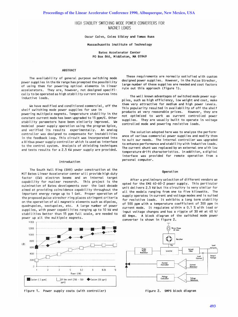
After a prel iminary selection of different vendors we opted for the EMS 40-60-2 power supply. This particular unit del ivers 2.5 kW but its circuitry is very simi lar for all the models ranging from one to five kilowatts. The suppl y operates in current and vol tage modes and is sui ted for resistive loads. It exhibits a long term stability of 500 ppm with a temperature coefficient of 300 ppm in current mode. It regulates within a 0.1 % with load or input voltage changes and has a ripple of 30 mV at 40 VI 60 Amps. A block diagram of the switched mode power converter is shown in figure 2.
Figure 2. SMPS block diagram
Proceedings of the Linear Accelerator Conference 1990, Albuquerque, New Mexico, USA
493

The three phase input AC is rectified and filtered to provide an unregulated voltage (265V - 350V) DC bus, which is converted into a high frequency square wave through a high frequency power transformer. This AC is then rectified and filtered to provide a low level DC output. Control of the output vol tage or current levels is ach i eved by modifying the duty cycle of the high frequency AC voltage.
In the current controlled mode, the output current must be sampled and compared with a reference. The error signal is sent to integrated PWM controllers (UC3524), operating in the master slave mode. They control the duty cycle of the drivers, which are magnetically coupled to the output stage.
I n order to operate the Power Suppl y wi th the des ired long and short term stability of fifteen parts per million, some critical components must be improved. It can be easily proven that in a feedback loop, if enough gain is provided in the direct loop, the elements that determine the accuracy and stability of the system are the transductor, the reference and the error amplifier.
The internal shunt, made of Manganin,with a temperature coefficient of 150 ppm was unsatisfactory. A zero flux transductor would be appropiate to monitor the high output current but its cost becomes prohibitive when large number of them are required. Instead, a more inexpensive unit, a resistive shunt made of Zeranin, was utilized. These shunts exhibit a temperature coefficient better than five parts per million per degree Celsius over the range of 00 C to +60 0 C. The shunt is water cooled and the temperature of the water is kept within one degree Celsius. The unit tested dissipated up to 100 Watts, del ivering one volt at 100 Amps. This signal is amplified by a low noise instrumentation amplifier.
The internal reference was also replaced by an external one, with very low drift (0.6 ppm)! and excellent line regulation (2ppm/V). The reference feeds a sixteen bit Digital to Analog converter that can be set remotely from a computer. The output of the DAC is used to provide the current reference to the power supply.
The error amplifier was upgraded to a low drift instrumentation ampl ifier providing very high gain (140db) at low frequencies, thereby reducing the errors in the stationary state. The original current and vol tage regulators were coupled with diodes to the Pulse Width Modul ator, and by us i ng the same method to incorporate our upgraded controller to the loop we avoided the need to modify the power supply motherboard.
Modelling and compensation
The supply used in our tests operates in a full bridge configuration as a Buck converter. A simplified diagram of th i s type of converter is shown in figure 3. The inductor is energized when the transistors are conducting, with a slope given by Vi-Vall, and discharges across the capacitor and load when the transistors are off, with a slope given by -Vall.
Using two state averaged differential equations, a simplified model for the PWM can be easily derived [ref 3 and 4]. This model replaces the PWM with a Vol tage source that depends on the duty cycle "d" and a filter as shown in figure 4.
d'Vp
--VO!LI
\
----------1) 1
Figure 3. Simplified Buck Converter 1 Ll I
1 3 ) ~-.-~~~
Figure 4. Simplified model for the PWM The internal shunt was originally placed before the
output filter capacitor and, even though the average current across the capacitor should be zero, a temperature dependent leakage current was measured which affected the regulation. Placing the shunt resistor in series with the load solves this problem but increases the order of the transfer function and the internal compensators were no longer appropriate.
Solving the current and voltage expressions for the circuit in figure 4, the transfer function between the output current and the control signal is:
G(s) (1 + S C2 R2) (sZ l1 C2 + s R2 C2 + 1)(s l3/R3 +1)
By inspecting the previous equation, it can be seen that the PWM presents a zero introduced by the capacitor with its ESR, it has a complex poles produced by the fi l ter lC and extra pole introduced by the load. Replacing the components by its numeric values the roots are as follows:
poles:
p1,2 p3
zero: Z1
-362.7 +1- 664.52i -10.114
-800
(fn (f3
121 Hz) 1.6 Hz)
(f1 = 127 Hz)
An external compensator was designed with three lead and one lag circuit. The first lead has a zero to cancel the pole introduced by the load. The second lead has it zero cancelling one of the complex poles. The third lead was placed at high frequencies to improve the phase margin, and the lag circuit introduces a pole at the origin to integrate any possible dc error. The gain was chosen to obtained a closed loop response with a frequency bandwidth of two kilohertz.
The design was verified with a model developed in Spice (Figure 5). Figure 6 is a Bode Plot that compares the models (Spice and Mathematica) with the values measured experimentally with 4 mH Magnet load.
Proceedings of the Linear Accelerator Conference 1990, Albuquerque, New Mexico, USA
494

Figure 5. Spice model of the upgraded power supply Anoplitude (db) Phow (<H-qrHS)
20
10
-10
-20
-30
- 40
-50
-60
100
t---------v------t--'f--;O"r---+--~~~ ··45
t---------f======---~~~~~--------~-oo t------j------f-------=:1y--,-.-::=---+ -'35
L-____ -L _____ L-____ ~_~d-_~ _ 'OO
'0 ' 00 '000 '0000
Figur~ 6. Open Loop Frequency Response of the PWM
sh ttern ~ 1/\ / ~, I. ~ rIM, rv' ~~ 4:C k7.? 'r l\W~
/'w I ~ , 'oc~ tern .
~' I )r ~ fA";" ( .. \'{~ :\\,ft, ;;,
kLf" "'T r: A/ "Pili Ufl "fI'e' i"Pu,
1/\ I t, "'Ill:
17\ r rQI ~ ." f"'-shunt volloq
~ V
fj/'i i''''''\
-----~ . {tAt":; ~J\V
~ l, ,\ / 1/1" 'I, ~ ''Ii'' \1 r,
~l 00'1
.\/,. ;.: :'-. ~~ ,~f./. ;
~/Ji;i) ; . ." '·n
05
-05
della -I
-2
-25
-70 ppmO 10
-3
hours Figure 7. Experimental results
Shielding
The shielding techniques for the controller are critical to the succesful operation of the power supply. This is obvious for any high gain, low signal amplifier. Three basic rules for shielding techniques were followed [see ref.6]. First, all shields and enclosures must be tied to a zero reference to be effective. The enclosures for the power supply, analog controller and power shields are all tied to earth ground. The shields for the signals and the analog ground plane are all tied to the controller zero reference in the power supply. Since the output of the supply must be floating, the analog shield and the earth shields are capacitively coupled. The analog shields must drain current away amplifier inputs, i.e. toward the source. They should also be configured to avoid ground loops from shield to shield so no daisey chaining of the shields is allowed. Each shield is connected at
the same point in the controller, which is also connected to the signal cOlll1lOn in the power supply. Separate shields for each i ndependant signa l into or out of the cont ro II er box and an additional shield for the power entrance was provided.
Several configurations of the ground and shield connections were tried. The setup in figure 8 has had the best results. A Ferrite core was needed in the shunt cable to reduce the high frequency cOlll1lOn mode noise entering the controller from that point.
r----------------- ----------i
r- - --,/-'-1.' ___ __
, Error amplifier i BATES Shunt amplifier I DIGITAL DAC
I ,
: Board DC - DC converter i 1 ,
1 __ ___ _ -' 1 '
, ' L-______ -1~~r_-_-_-_-_-_~_~_~_~_~_~_~_~_~_~_~_~_~_-_~ __ i Figure 8. Shielding techniques
Cone l us i ons
Power uni ts from di fferent manufacturers where tri ed out and the circuit developed was modified only sligthly to regulate properly. Power levels ranged from 1 to 2.5 kWatts . Some noise is still measured in the prototype version and the shielding needs to be improved . Some of the problems observed in the prototype wi II be sol ved when a pc board is developed with proper ground planes for digital and analog signals. Analysis is been developed to build a state vari able feedback type of controller. By using feedback from the internal shunt and also from the output voltage, we believe that the compensator can be reduced to simple coefficients, improving the dynamic response and simplifying the des i gn.
References
1. T. Russ, C. Sibley, "A distributed Power-Supply Controller using the Bitbus interface' " Nuclear Instruments and Methods in Physics Research", A293, 1990.
2. D. Mitchell, " Switching Regulator Analysis", McGraw Hill Book Company, ISBN 0-07-042597-3
3. R. Middlebrook and S. Cuk, " A general Unified Approach to Modell i ng Swi tching Converter Power Stages' , , IEEE Power Electronics Specialists Conference Record, June 1976, pp. 18-34.
4. Switched Mode Power Supply Transfer Determination using Spice", IEEE Power Electronics Special ists Conference Record, june 1984, pp. 297-303.
5. Instruction manual for EMS power supply 40-60-2, Electronic measurements, Neptune, NJ.
6. R. Morrison, "grounding and shielding Techniques in instrumentation",John Wiley & Sons, 1977.
Proceedings of the Linear Accelerator Conference 1990, Albuquerque, New Mexico, USA
495