High Speed SelectIO Wizard v3 · High Speed SelectIO Wizard v3.5 6 PG188 December 05, 2018 Chapter...
89
High Speed SelectIO Wizard v3.5 LogiCORE IP Product Guide Vivado Design Suite PG188 December 05, 2018
Transcript of High Speed SelectIO Wizard v3 · High Speed SelectIO Wizard v3.5 6 PG188 December 05, 2018 Chapter...

High Speed SelectIO Wizard v3.5
LogiCORE IP Product Guide
Vivado Design SuitePG188 December 05, 2018

High Speed SelectIO Wizard v3.5 2PG188 December 05, 2018 www.xilinx.com
Table of ContentsIP Facts
Chapter 1: OverviewFeature Summary. . . . . . . . . . . . . . . . . . . . . . . . . . . . . . . . . . . . . . . . . . . . . . . . . . . . . . . . . . . . . . . . . . 5Applications . . . . . . . . . . . . . . . . . . . . . . . . . . . . . . . . . . . . . . . . . . . . . . . . . . . . . . . . . . . . . . . . . . . . . . 6Unsupported Features. . . . . . . . . . . . . . . . . . . . . . . . . . . . . . . . . . . . . . . . . . . . . . . . . . . . . . . . . . . . . . 6Licensing and Ordering . . . . . . . . . . . . . . . . . . . . . . . . . . . . . . . . . . . . . . . . . . . . . . . . . . . . . . . . . . . . . 6
Chapter 2: Product SpecificationPerformance. . . . . . . . . . . . . . . . . . . . . . . . . . . . . . . . . . . . . . . . . . . . . . . . . . . . . . . . . . . . . . . . . . . . . . 8Resource Utilization. . . . . . . . . . . . . . . . . . . . . . . . . . . . . . . . . . . . . . . . . . . . . . . . . . . . . . . . . . . . . . . . 8Port Descriptions . . . . . . . . . . . . . . . . . . . . . . . . . . . . . . . . . . . . . . . . . . . . . . . . . . . . . . . . . . . . . . . . . . 8
Chapter 3: Designing with the CoreGeneral Design Guidelines . . . . . . . . . . . . . . . . . . . . . . . . . . . . . . . . . . . . . . . . . . . . . . . . . . . . . . . . . 19Clocking. . . . . . . . . . . . . . . . . . . . . . . . . . . . . . . . . . . . . . . . . . . . . . . . . . . . . . . . . . . . . . . . . . . . . . . . . 19Resets . . . . . . . . . . . . . . . . . . . . . . . . . . . . . . . . . . . . . . . . . . . . . . . . . . . . . . . . . . . . . . . . . . . . . . . . . . 25Protocol Description . . . . . . . . . . . . . . . . . . . . . . . . . . . . . . . . . . . . . . . . . . . . . . . . . . . . . . . . . . . . . . 27
Chapter 4: Design Flow StepsCustomizing and Generating the Core . . . . . . . . . . . . . . . . . . . . . . . . . . . . . . . . . . . . . . . . . . . . . . . . 28Output Generation. . . . . . . . . . . . . . . . . . . . . . . . . . . . . . . . . . . . . . . . . . . . . . . . . . . . . . . . . . . . . . . . 73Constraining the Core . . . . . . . . . . . . . . . . . . . . . . . . . . . . . . . . . . . . . . . . . . . . . . . . . . . . . . . . . . . . . 74Simulation . . . . . . . . . . . . . . . . . . . . . . . . . . . . . . . . . . . . . . . . . . . . . . . . . . . . . . . . . . . . . . . . . . . . . . 75Synthesis and Implementation . . . . . . . . . . . . . . . . . . . . . . . . . . . . . . . . . . . . . . . . . . . . . . . . . . . . . . 75
Chapter 5: Example Design
Chapter 6: Test Bench
Appendix A: Verification, Compliance, and InteroperabilitySimulation . . . . . . . . . . . . . . . . . . . . . . . . . . . . . . . . . . . . . . . . . . . . . . . . . . . . . . . . . . . . . . . . . . . . . . 79Hardware Testing. . . . . . . . . . . . . . . . . . . . . . . . . . . . . . . . . . . . . . . . . . . . . . . . . . . . . . . . . . . . . . . . . 79
Send Feedback

High Speed SelectIO Wizard v3.5 3PG188 December 05, 2018 www.xilinx.com
Appendix B: UpgradingUpgrading in the Vivado Design Suite . . . . . . . . . . . . . . . . . . . . . . . . . . . . . . . . . . . . . . . . . . . . . . . . 80
Appendix C: DebuggingFinding Help on Xilinx.com . . . . . . . . . . . . . . . . . . . . . . . . . . . . . . . . . . . . . . . . . . . . . . . . . . . . . . . . . 81Vivado Design Suite Debug Feature . . . . . . . . . . . . . . . . . . . . . . . . . . . . . . . . . . . . . . . . . . . . . . . . . . 82Hardware Debug . . . . . . . . . . . . . . . . . . . . . . . . . . . . . . . . . . . . . . . . . . . . . . . . . . . . . . . . . . . . . . . . . 83
Appendix D: Additional Resources and Legal NoticesXilinx Resources . . . . . . . . . . . . . . . . . . . . . . . . . . . . . . . . . . . . . . . . . . . . . . . . . . . . . . . . . . . . . . . . . . 84Documentation Navigator and Design Hubs . . . . . . . . . . . . . . . . . . . . . . . . . . . . . . . . . . . . . . . . . . . 84References . . . . . . . . . . . . . . . . . . . . . . . . . . . . . . . . . . . . . . . . . . . . . . . . . . . . . . . . . . . . . . . . . . . . . . 85Revision History . . . . . . . . . . . . . . . . . . . . . . . . . . . . . . . . . . . . . . . . . . . . . . . . . . . . . . . . . . . . . . . . . . 86Please Read: Important Legal Notices . . . . . . . . . . . . . . . . . . . . . . . . . . . . . . . . . . . . . . . . . . . . . . . . 89
Send Feedback

High Speed SelectIO Wizard v3.5 4PG188 December 05, 2018 www.xilinx.com Product Specification
IntroductionThe LogiCORE™ IP High Speed SelectIO™ wizard simplifies the integration of SelectIO technology into high-speed system designs for UltraScale™ and UltraScale+™ devices. This wizard creates a Verilog HDL file that instantiates and configures I/O and clocking logic such as RX_BITSLICE, TX_BITSLICE, RXTX_BITSLICE, BITSLICE_CONTROL and PLL blocks present in the physical-side interface (PHY) architecture. Additionally, this core provides pin planning for the configured interface and updates the register transfer level (RTL) based on constraints.
Features• User selectable interface types such as TX
only, RX only and a mix of TX, RX and BiDir (Beta) bus directions
• For RX and BiDir (Beta) interfaces, the clock/strobe to data relationship is selectable according to the protocol setting
• Supports serialization factor of 8 (Div4) and 4 (Div2)
• Phase-locked loop (PLL) clock source can be from either the global clock (GC) pin or from the interconnect driven through BUFG
• Range of the user selectable PLL input clock frequencies for a given data speed
• Configurable I/O delays• Optional register interface unit (RIU)
interface and bitslip logic• Bank selection and pin planning of all the
available pins in the bank with design rule checks to meet SelectIO Logic requirement
IP Facts
LogiCORE IP Facts TableCore Specifics
Supported Device Family(1)
Virtex® UltraScale+, Kintex® UltraScale+,Zynq® UltraScale+, Virtex UltraScale,
Kintex UltraScaleSupported User Interfaces RIU
Resources Performance and Resource Utilization web page
Provided with CoreDesign Files RTLExample Design VerilogTest Bench VerilogConstraints File Xilinx® Design Constraints (XDC)Simulation Model Not Provided
Supported S/W Driver(2) N/A
Tested Design Flows(3)
Design Entry Vivado® Design Suite
Simulation For supported simulators, see theXilinx Design Tools: Release Notes Guide.
Synthesis Vivado SynthesisSupport
Provided by Xilinx at the Xilinx Support web page
Notes: 1. For a complete list of supported devices, see the Vivado IP
catalog.2. Standalone driver details can be found in the software
development kit (SDK) directory (<install_directory>/SDK/<release>/data/embeddedsw/doc/xilinx_drivers.htm). Linux OS and driver support information is available from the Xilinx Wiki page.
3. For the supported versions of the tools, see theXilinx Design Tools: Release Notes Guide.
Send Feedback

High Speed SelectIO Wizard v3.5 5PG188 December 05, 2018 www.xilinx.com
Chapter 1
OverviewThe High Speed SelectIO™ wizard provides the source HDL wrapper for TX, RX and RXTX bitslices in native mode. The wizard also generates LOC constraints for synthesis and implementation runs.
Feature SummaryConfiguration• Configures bus direction, RX External Clock and Data, Interface speed, PLL clock source,
PLL input clock frequency, data width, bank, delay type/delay values on the TX/RX pins, data 3-state and strobe/clock 3-state
• Additionally RIU interface, PLL DRP interface, and Bitslip can be configured
Pin SelectionFor each byte group, configures the pin selection, bus direction, signal type, data/strobe, and signal name. Allows you to choose the TX/RX/Bidir bus direction with the same configuration.
Each I/O bank contains 52 pins that can be configured as TX/RX/BIDIR. The wizard provides pin level configurability for the following;
• TX/RX/BIDIR• Single ended/Differential• Data/strobe/input clock/Clock forward • Customizable signal name• Power-on value of serial lines of TX/RXTX pins• Reset state machine for initialization
Send Feedback

High Speed SelectIO Wizard v3.5 6PG188 December 05, 2018 www.xilinx.com
Chapter 1: Overview
ApplicationsThis solution is useful for high-speed I/O interface requirements like ASIC emulation and chip-to-chip interaction and any serial protocols operating at line rates from 300 Mb/s to 1,600 Mb/s.
Unsupported Features• Count mode (delay format)• Dynamic Phase Alignment (DPA) feature in the example design
Licensing and OrderingThis Xilinx® LogiCORE™ IP module is provided at no additional cost with the Xilinx® Vivado® Design Suite under the terms of the Xilinx End User License. Information about this and other Xilinx LogiCORE IP modules is available at the Xilinx Intellectual Property page. For information about pricing and availability of other Xilinx LogiCORE IP modules and tools, contact your local Xilinx sales representative.
Send Feedback

High Speed SelectIO Wizard v3.5 7PG188 December 05, 2018 www.xilinx.com
Chapter 2
Product SpecificationEach I/O bank in UltraScale™ devices contains 52 pins that can be used for input, output, or bidirectional. The High Speed SelectIO™ wizard provides various options to generate a wrapper using TX_BITSLICE, RX_BITSLICE, RXTX_BITSLICE, and BITSLICE_CONTROL for the user selected configuration in native mode. This wizard also configures clocking circuitry using PLL. A representative design using TX_BITSLICE, RX_BITSLICE, RXTX_BITSLICE and BITSLICE_CONTROL is shown in Figure 2-1.
The HDL wrapper instantiates all the bitslices related to an I/O bank. Depending on the pin selected, corresponding bitslices are connected to the general interconnect and I/Os. The wizard also provides LOC constraints to the top level ports.
X-Ref Target - Figure 2-1
Figure 2-1: Representative Design
Send Feedback

High Speed SelectIO Wizard v3.5 8PG188 December 05, 2018 www.xilinx.com
Chapter 2: Product Specification
PerformanceThe HSSIO wizard performance is measured by the data speed that it can support, which in turn is the capability realized in the selected I/Os of the device. Refer to the UltraScale Architecture SelectIO Resources: Advance Specification User Guide (UG571) [Ref 1] for more details on the performance characteristics.
This core supports a maximum data speed of 1,600 Mb/s for serialization factor 8 and 1,600 Mb/s for serialization factor 4. The general interconnect logic works at 1/8 or 1/4 clock of the interface speed clock.
Resource UtilizationFor more details on performance and resource utilization, visit the Performance and Resource Utilization web page
This core uses a flip-flop to generate clkoutphyen of the PLL for the circuit stabilization before the actual data is sent on the I/O. Other blocks used are FPGA hard blocks.
Port DescriptionsTable 2-1 and Table 2-2 describe the input and output ports of the High Speed SelectIO wizard. Availability of ports is controlled by user selection.
Table 2-1 lists ports that are top-level ports connected to the FPGA I/O. The renaming feature is useful for multiple instances of the core in the design to avoid conflicting pin LOC constraints.
Table 2-1: Ports Connected to FPGA I/O
Port Direction Clock Domain Description
Global Ports
clk_p Input NA Differential clock input P connected to PLL. The port is available only when a PLL is instantiated in the core.
clk_n Input NA Differential clock input N connected to PLL. The port is available only when a PLL is instantiated in the core.
clk Input NA Single ended clock connected to PLL. The port is available only when a PLL is instantiated in the core.
Send Feedback

High Speed SelectIO Wizard v3.5 9PG188 December 05, 2018 www.xilinx.com
Chapter 2: Product Specification
rst Input riu_clk
Global reset pin. When RIU_CLK is a free running clock, Assertion of the reset is asynchronous. De-assertion is synchronous with respect to the RIU clock.Minimum pulse width should be 5 ns. If RIU_CLK is derived from the same PLL as XiPHY, then the rst signal needs to be pulsed asynchronously for a minimum of 5ns. Refer to the PLL Switching Characteristics section in the Kintex UltraScale Architecture Data Sheet (DS892) [Ref 2].
bg<x>_pin<y>_<pin num>Input/Output/Inout
NA
Data/Input Clock/Strobe/Clk forward ports connected to I/O pins. Port name of the wizard IP is user-specified through the Vivado® Integrated Design Environment (IDE) appended with the pin number in the bank when Append Pin No. to IOs is selected. To elaborate, the wizard appends the pin_num (range from 0 - 51, number of pins in a full bank) to the port name during generation. The default port name is bg<x>_pin<y>_<pin num>. (You can overwrite the default port name from its default value.) In this naming convention, x indicates the byte group and its value ranges from 0 to 3 and y indicates the pin position within the bytegroup and its value ranges from 0-12. For example, if you select the 13th pin and the signal name is bg1_pin0, the actual port name is bg1_pin0_13 and the corresponding signal name to the interconnect end would be data_from_fabric_bg1_pin10_13 or data_to_fabric_bg1_pin10_13 depending on the direction of the pin chosen.
bg<x>_pin<y>_nc Input NA
Inferred bitslice ports. The wizard infers bitslice0 of a nibble for strobe propagation within the bytegroup; <x> indicates bytegroup (0,1,2,3); <y> indicates bitslice0 position (0 in case of lower nibble, 6 in case of upper nibble.) There is no need to drive any data on these ports. The ports must be connected when instantiating the design and brought to the top-level hierarchy to ensure proper functionality of the inferred bitslices. Note: This IOB is not available for any other usage.Refer to the UltraScale Architecture SelectIO Resources: Advance Specification User Guide (UG571) [Ref 1] for Clocking guidelines.
Table 2-1: Ports Connected to FPGA I/O (Cont’d)
Port Direction Clock Domain Description
Send Feedback

High Speed SelectIO Wizard v3.5 10PG188 December 05, 2018 www.xilinx.com
Chapter 2: Product Specification
Table 2-2: Ports Connected to FPGA General Interconnect LogicPort Direction Clock Domain Description
Data Ports
data_from_fabric_<sig_name>_<y> [sf -1:0] Input pll0_clkout0 or app_clk
Parallel data input from the interconnect logic to TX/Bidir TX bitslices. <sig_name> is the signal name configured for TX/Bidir bus direction during customization.<y> is the pin number (range from 0 -51) appended by the wizard when Append Pin No. to IOs is selected. sf is the serialization factor.
data_to_fabric_<sig_name>_<y>[sf-1:0] Output pll0_clkout0 or app_clk
Parallel data output to general interconnect logic from RX/Bidir RX bitslices. <sig_name> is the signal name configured for RX/Bidir bus direction during customization.<y> is the pin number (range from 0 to 51) appended by the wizard when Append Pin No. to IOs is selected. sf is the serialization factor. For differential RX pins, the parallel data corresponding to the N pin is also available.
Clock Ports
pll0_clkout0 Output NA
Divided version of clock from PLL CLKOUT0 for the general interconnect logic. The frequency of this is data speed divided by the serialization factor. This clock can be used as a clock for the general interconnect logic.
pll0_clkout1 Output NA
Divided version of the clock from PLL CLKOUT1 for the general interconnect logic from PLL0. The frequency of this can be set in Vivado IDE from a list of supported frequencies for the data speed chosen.
pll1_clkout0 Output NA
Divided version of the clock from PLL CLKOUT0 for the general interconnect logic from PLL1. The frequency of this can be set in Vivado IDE from a list of supported frequencies for the data speed chosen.
clock_from_ibuf Output NA
This port is available only when Rx Clock to Data Alignment is set to Async/None and the PLL Clock Source is through a GC pin. The Clock output from the Input Buffer is given as an external port.
Send Feedback

High Speed SelectIO Wizard v3.5 11PG188 December 05, 2018 www.xilinx.com
Chapter 2: Product Specification
RX/Bidir RX Delay Control Ports
rx_clk Input NA DELAY clock used to sample LOAD, CE and INC for RX.
rx_cntvalue_in_<i> [8:0] Input rx_clk/bidir_rx_clk
Counter value from the FPGA logic for dynamically loadable tap value for RX. <i> is the corresponding pin number on which the RX/Bidir bus direction is selected.
rx_cntvalue_out_<i>[8:0] Output rx_clk/bidir_rx_clk
Counter value going to FPGA logic for monitoring the tap value for RX. <i> is the corresponding pin number on which the RX/Bidir bus direction is selected.
rx_ce_<i> Input rx_clk/bidir_rx_clk
Clock enable for the IDELAY register clock for RX. <i> is the corresponding pin number on which the RX/Bidir bus direction is selected.
rx_en_vtc<i> Input rx_clk/bidir_rx_clk
Active-High to enable DELAYCTRL to keep delay over voltage and temp to load new delay for RX Delay Control. <i> is the pin number on which the RX/Bidir bus direction is selected.
rx_inc<i> Input rx_clk/bidir_rx_clkIncrement the current delay tap setting for RX. <i> is the pin number on which the RX/Bidir bus direction is selected.
rx_load<i> Input rx_clk/bidir_rx_clkLoad the count value from CNTVALUEIN for RX. <i> is the pin number on which the RX/Bidir bus direction is selected.
RX Extended Delay Control Ports
rx_cntvalue_in_ext_<i>[8:0] Input rx_clk
Extended counter value from the FPGA logic for dynamically loadable tap value for RX. <i> is the corresponding pin number on which the RX bus direction is selected.
rx_cntvalue_out_ext_<i>[8:0] Output rx_clk
Extended counter value going to the FPGA logic for monitoring the tap value for RX. <i> is the corresponding pin number on which the RX bus direction is selected.
Table 2-2: Ports Connected to FPGA General Interconnect Logic (Cont’d)
Port Direction Clock Domain Description
Send Feedback

High Speed SelectIO Wizard v3.5 12PG188 December 05, 2018 www.xilinx.com
Chapter 2: Product Specification
rx_ce_ext_<i> Input rx_clk
Extended clock enable for the IDELAY register clock for RX. <i> is the corresponding pin number on which the RX bus direction is selected.
rx_en_vtc_ext_<i> Input rx_clk
Extended active-High to enable DELAYCTRL to keep delay over voltage and temp to load new delay for RX Delay Control. <i> is the pin number on which the RX bus direction is selected.
rx_inc_ext_<i> Input rx_clkExtended increment the current delay tap setting for RX. <i> is the pin number on which the RX bus direction is selected.
rx_load_ext_<i> Input rx_clkExtended load count value from CNTVALUEIN for RX. <i> is the pin number on which the RX bus direction is selected.
TX/Bidir TX Delay Control Ports
tx_clk Input NA DELAY clock used to sample LOAD, CE INC for TX.
tx_cntvalue_in_<i>[8:0] Input tx_clk/bidir_tx_clk
Counter value from the FPGA logic for dynamically loadable tap value for TX. <i> is the corresponding pin number on which the TX/Bidir bus direction is selected.
tx_cntvalue_out_<i>[8:0] Output tx_clk/bidir_tx_clk
Counter value going to the FPGA logic for monitoring the tap value for TX. <i> is the corresponding pin number on which the TX/Bidir bus direction is selected.
tx_ce_<i> Input tx_clk/bidir_tx_clk
Clock enable for the ODELAY register clock for TX. <i> is the corresponding pin number on which the TX/Bidir bus direction is selected.
tx_en_vtc<i> Input tx_clk/bidir_tx_clk
Active-High to enable DELAYCTRL to keep delay over voltage and temp to load new delay for TX Delay Control. <i> is the pin number on which the TX/Bidir bus direction is selected.
tx_inc<i> Input tx_clk/bidir_tx_clkIncrement the current delay tap setting for TX. <i> is the pin number on which the TX/Bidir bus direction is selected.
Table 2-2: Ports Connected to FPGA General Interconnect Logic (Cont’d)
Port Direction Clock Domain Description
Send Feedback

High Speed SelectIO Wizard v3.5 13PG188 December 05, 2018 www.xilinx.com
Chapter 2: Product Specification
tx_load<i> Input tx_clk/bidir_tx_clkLoad the count value from CNTVALUEIN for TX. <i> is the pin number on which the TX/Bidir bus direction is selected.
Bidir Delay Clock Ports
bidir_tx_clk Input NA DELAY clock used to sample LOAD, CE, INC for TX
bidir_rx_clk Input NA DELAY clock used to sample LOAD, CE, INC for RX
TXBITSLICE_TRI Delay Control Ports
bidir_tx_bs_tri_clk Input bidir_tx_clk Delay Clock used to sample LOAD, CE, INC
bidir_tx_bs_tri_cntvaluein<n>[8:0] Input bidir_tx_clk
Counter value from the FPGA logic for dynamically loadable tap value, 1 per nibble, <n> indicates the nibble number that varies from 0 to 7.
bidir_tx_bs_tri_cntvalueout<n>[8:0] Output bidir_tx_clk
Counter value to the FPGA logic for monitoring the tap value of the delay control, 1 per nibble, <n> indicates the nibble number that varies from 0 to 7.
bidir_tx_bs_tri_ce<n> Input bidir_tx_clkClock Enable for the ODELAY register clock, 1 per nibble, <n> indicates the nibble number that varies from 0 to 7.
bidir_tx_bs_tri_en_vtc<n> Input bidir_tx_clk
Active-High to enable DELAYCTRL to keep delay over voltage and temp to load a new delay for TXBITSLICE TRI Delay Control. <n> indicates the nibble number that varies from 0 to 7.
bidir_tx_bs_tri_inc<n> Input bidir_tx_clkIncrement the current delay tap setting, 1 per nibble. <n> indicates the nibble number that varies from 0 to 7.
bidir_tx_bs_tri_load<n> Input bidir_tx_clkLoad the count value from CNTVALUEIN, 1 per nibble. <n> indicates the nibble number that varies from 0 to 7.
Table 2-2: Ports Connected to FPGA General Interconnect Logic (Cont’d)
Port Direction Clock Domain Description
Send Feedback

High Speed SelectIO Wizard v3.5 14PG188 December 05, 2018 www.xilinx.com
Chapter 2: Product Specification
3-State Ports
tri_tbyte<n>[3:0] Input pll0_clkout0 or app_clk
Serialized 3-state input, 1 per nibble, <n> indicates the nibble number that varies from 0 to 7.When data_tri=0 or clk_tri is enabled, these ports are only used for tri_bitslice_tri functionality not for the multi_bank interface feature.Note: For multi bank feature these ports are available.
tri_t<i> Input pll0_clkout0 or app_clkCombinatorial Data 3-State input, 1 per bitslice. <i> is the pin number on which the BiDir or Tx bus is selected.
RIU Ports
riu_addr_bg<m>[5:0] Input riu_clkAddress of the RIU register. <m> indicates bytegroup. Varies from 0 to 3.
riu_clk Input NA
System clock from the general interconnect. <m> indicates bytegroup. Varies from 0 to 3. You can choose to generate the riu_clk from the PLL through a Vivado IDE selection. PLL_CLKOUT1 is used as the source for riu_clk. The presence of riu_clk is mandatory for the design.
riu_nibble_sel_bg<m>[1:0] Input riu_clkNibble select to enable RIU read/write for upper (Logic 1 or lower nibble 0). <m> indicates bytegroup. Varies from 0 to 3.
riu_wr_data_bg<m>[15:0] Input riu_clkInput write data to the register. <m> indicates bytegroup. Varies from 0 to 3.
riu_wr_en_bg<m> Input riu_clkRegister write enable active-High. <m> indicates bytegroup. Varies from 0 to 3.
riu_rd_data_bg<m>[15:0] Output riu_clkOutput read data to the controller. <m> indicates bytegroup. Varies from 0 to 3.
riu_valid_bg<m> Output riu_clkOutput read valid to the controller. <m> indicates bytegroup. Varies from 0 to 3.
Status/Control
Table 2-2: Ports Connected to FPGA General Interconnect Logic (Cont’d)
Port Direction Clock Domain Description
Send Feedback

High Speed SelectIO Wizard v3.5 15PG188 December 05, 2018 www.xilinx.com
Chapter 2: Product Specification
pll0_locked Output NA Logic High indicates PLL is locked to the desired clock frequency.
dly_rdy_bsc<n> Output riu_clk Indicates fixed delay calibration completion.
vtc_rdy_bsc<n> Output riu_clkPHY calibration is complete (VTC is ready – after EN_VTC is enabled).Note: VTC is Voltage and Temperature Control.
en_vtc_bsc<n> Input riu_clkActive-High to enable DELAYCTRL to keep delay over voltage and temp low to load new delay.
fifo_empty_<i> Output pll0_clkout0 or app_clkFIFO empty flag from each bitslice. <i> is the pin number on which the RX/Bidir RX is selected.
fifo_rd_en_<i> Input pll0_clkout0 or app_clk
FIFO read enable for each bit slice. <i> is the pin number on which the RX/Bidir RX is selected. This port is available only when the FIFO RD EN user control option is enabled in Vivado IDE.
fifo_rd_clk_<i> Input pll0_clkout0 or app_clkFIFO read clock for each bitslice. <i> is the pin number on which the RX/Bidir RX is selected.
fifo_rd_data_valid Output fifo_rd_clkValidated the data_to_fabric bus. This port is available only when FIFO Read Enable user control is disabled in Vivado IDE.
start_bitslip Input Not applicable
Reset for the bitslip logic. Active-Low. When the top level rst pin is asserted, start_bitslip should be driven Low. The start_bitslip port should be deasserted only when the Transmit partner of the serial line is transmitting the bitslip training pattern.
bitslip_error_<i> Output fifo_rd_clk_<i>
Error output for bitslip. When eight bitslips are performed for 8-bit serialization or four bitslips are performed for 4-bit serialization, this output is pulsed High.
rxtx_bitslip_sync_done Output fifo_rd_clkIndicates that the bitslip training pattern is received at all bidirectional pins in the design.
rx_bitslip_sync_done Output fifo_rd_clkIndicates that the bitslip training pattern is received at all RX pins in the design.
Table 2-2: Ports Connected to FPGA General Interconnect Logic (Cont’d)
Port Direction Clock Domain Description
Send Feedback

High Speed SelectIO Wizard v3.5 16PG188 December 05, 2018 www.xilinx.com
Chapter 2: Product Specification
fifo_wr_clk_<n> Output NA
FIFO write clock from the bitslice0 of each nibble on which the strobe is available. This pin is available only if PLL0_FIFO_WRITE_CLK_OUT is chosen in Vivado IDE.
rst_seq_done Output riu_clk
Indicates that the reset sequence is completed and the wizard is ready. When this signal is asserted High, transactions can be initiated from the general interconnect logic.
shared_pll0_clkout0_in Input Not applicable
This port is available when you choose to instantiate the PLL in the example design. The pll0_clkout0 signal from the master core is given as an input to slave core.
shared_pll1_clkout0_in Input Not applicable
This port is available when you choose to instantiate the PLL in the example design. The pll1_clkout0 signal from the master core is given as an input to the slave core.
shared_pll0_clkoutphy_in Input Not applicable
This port is available when you choose to instantiate the PLL in the example design. The pll0_clkoutphy signal from the master core is given as an input to the slave core.
shared_pll1_clkoutphy_in Input Not applicable
This port is available when you choose to instantiate the PLL in the example design. The pll1_clkoutphy signal from the master core is given as an input to the slave core.
shared_pll0_locked_in Input Not applicable
This port is available when you choose to instantiate the PLL in the example design. The pll0_locked signal from the master core is given as an input to the slave core.
shared_pll1_locked_in Input Not applicable
This port is available when you choose to instantiate the PLL in the example design. The pll1_locked signal from the master core is given as an input to the slave core.
shared_pll0_clkoutphy_out Output Not applicable
This port is available when you choose to instantiate the PLL in the core. The pll0_clkoutphy signal from the master core is given as an output to the slave core.
Table 2-2: Ports Connected to FPGA General Interconnect Logic (Cont’d)
Port Direction Clock Domain Description
Send Feedback

High Speed SelectIO Wizard v3.5 17PG188 December 05, 2018 www.xilinx.com
Chapter 2: Product Specification
shared_pll1_clkoutphy_out Output Not applicable
This port is available when you choose to instantiate the PLL in the core. The pll1_clkoutphy signal from the master core is given as an output to the slave core.
app_clk Input Not Applicable
This port is available when Enable ports to connect Multiple Interfaces is selected. This is the clock used to drive the fabric side ports.
intf_rdy Output RIU CLK
This port is available when Enable ports to connect Multiple Interfaces is selected. It indicates that the reset sequence of the interface is done.
multi_intf_lock_in Input Not Applicable
This port is available when Enable ports to connect Multiple Interfaces is selected. This is an AND of PLL_LOCKs of all the interfaces which constitute the multi-interface design.
DRP Ports(1)
daddr [6:0] Input dclkDynamic Reconfiguration Address: Address port for use in dynamic reconfiguration; active when den is asserted.
dclk Input Not ApplicableDynamic Reconfiguration Clock: Clock port for use in dynamic reconfiguration.
den Input dclkDynamic Reconfiguration Enable: Starts a dynamic reconfiguration transaction. Refer to DRP protocol details for more information.
di [15:0] Input dclkDynamic Reconfiguration Data in: Input data for a dynamic reconfiguration write transaction; active when den is asserted.
do [15:0] Output dclkDynamic Reconfiguration Data Out: Output data for a dynamic reconfiguration read transaction; active when drdy is asserted.
drdy Output dclkDynamic Reconfiguration Ready: Completes a dynamic reconfiguration transaction
Table 2-2: Ports Connected to FPGA General Interconnect Logic (Cont’d)
Port Direction Clock Domain Description
Send Feedback

High Speed SelectIO Wizard v3.5 18PG188 December 05, 2018 www.xilinx.com
Chapter 2: Product Specification
dwe Input dclk
Dynamic Reconfiguration Write Enable: When asserted, indicates that the dynamic reconfiguration transaction is a write; active when den is asserted.
Notes: 1. For more information on DRP ports, see UltraScale Architecture Clocking Resources User Guide (UG572) [Ref 13].
Table 2-2: Ports Connected to FPGA General Interconnect Logic (Cont’d)
Port Direction Clock Domain Description
Send Feedback
High Speed SelectIO Wizard v3.5 19PG188 December 05, 2018 www.xilinx.com
Chapter 3
Designing with the CoreThis chapter includes guidelines and additional information to facilitate designing with the core.
General Design GuidelinesThis core is for high-speed UltraScale™ and UltraScale+™ architecture designs and can be configured for a data speed range of 300-1,600 Mb/s. The following steps are recommended for all designs using the High Speed SelectIO™ wizard.
You are expected to have the interface requirements of your application prior to generating the High Speed SelectIO (HSSIO) wizard specific to your designs — details such as interface speed, clock to data relationship, and system clocking structure. For example, what should be the source of the PLL input clock; board pin layout constraints are expected to be specified while generating with the wizard.
There can be two approaches that you can follow when it comes to pin planning. If there are no board layout restrictions, you can do the pin planning through the wizard, generate the wizard, and make sure the Vivado® design tools perform synthesis and implementation without any DRCs. You can also try to retrofit the board pin layout into the wizard pin planning. It is important to make sure the Vivado design tools complete the synthesis and implementation without any design rule checks (DRCs). In either approach, you must ensure that Vivado synthesis and implementation goes through without DRCs to avoid issues at the later stage of board design.
ClockingThe PLLs associated with each bank are the primary source for clocking the SelectIO resources in the bank. You can select the source of the input reference clock to PLL. The source can be a clock from the global clock pin (GC) or from the general interconnect through BUFG. You can also select the input clock frequency from Vivado IDE, which lists all the supported clocks for a given device.
Send Feedback

High Speed SelectIO Wizard v3.5 20PG188 December 05, 2018 www.xilinx.com
Chapter 3: Designing with the Core
PLL InstantiationYou are given the option in Vivado IDE to instantiate the PLL in the core or the example design. This provides ease of use to share the PLL across multiple designs in a single bank. The core that has the PLL instantiated inside it is called the master. Other instances of the wizard that do not have the PLL instance inside the core are called slaves. The interface between the master and slave cores is shown in Figure 3-1. Note that when generating the master and slave cores, the interface speed and other PLL parameters should remain the same.
Note: If the input clock source to PLL is from a GC pin, then the PLL sharing option is disabled. Because the "master" core will have the PLL driven by GC. Choose the input clock source as BUFG to PLL for the "slave" core.
Both, PLL0 and PLL1 are instantiated in the clk_scheme.v module. Based on the selection, clk_scheme.v is instantiated in the core or example design.
Note: For RX only designs, the option to instantiate the PLL in the example design is available only for the Edge double data rate (DDR) Strobe and Center DDR Strobe modes.
RIU ClockAn RIU Clock is mandatory for a design. The reset state machine and Bitslice control modules operate on the RIU clock. It can be provided through the riu_clk input port or generated internally from PLL0. You can choose the Generate RIU clock from PLL option in the Vivado IDE. Selecting this, enables the PLL_CLKOUT1 signal to be used as the RIU clock internally.
Clocking of TX_BITSLICEWhen transmitting data, the master input clock to the BITSLICE_CONTROL is used. The frequency of this clock determines the serial bit rate of data. Data is transmitted on the serial lines along with the associated clock or strobe. TX uses PLL0 by default unless RX operates in Serial Mode, when TX uses PLL1.
X-Ref Target - Figure 3-1
Figure 3-1: PLL Sharing
Master Core
PLL
Slave Core
shared_pll0_clkoutphy
shared_pll1_clkoutphy
shared_pll0_locked
shared_pll1_locked
shared_pll0_clkout0
shared_pll1_clkout0
Send Feedback

High Speed SelectIO Wizard v3.5 21PG188 December 05, 2018 www.xilinx.com
Chapter 3: Designing with the Core
The clock forwarding option in the wizard can be enabled on any pin in a given bank. The wizard supports any number of pins as Clock Forward pins. It is mandatory that the number of clock forward pins are less than or equal to the number of TX pins in the design. The phase of the forwarded clock with respect to the data can be set in Vivado IDE.
The Clock Forward pin acts as a Strobe/Clock for RX. The clock/strobe can be edge-aligned or center-aligned with the data. Clock/Strobe is generated similar to the data by applying a 01010101 pattern at the D[7:0] input of TX_BITSLICE / RXTX_BITSLICE. The alignment of the strobe to the data is achieved by setting the TX_OUTPUT_PHASE_90 attribute of the TX_BITSLICE/RXTX_BITSLICE.
Clocking of RX_BITSLICEPLL0 is the primary clock source for RX. There are two modes used to capture data in the RX_BITSLICEs initiated by an attribute of the BITSLICE_CONTROL component (SERIAL_MODE = TRUE/FALSE).
• When the attribute SERIAL_MODE is set to TRUE, the received data is captured using CLKOUTPHY from PLL0. This corresponds to the ASYNC/NONE and FRACTIONAL (Beta) options shown in Vivado IDE for the RX External Clock to Data Alignment. The receive data capture clock and receive data are either asynchronous, synchronous phase unknown, or non single data rate (SDR) or double data rate (DDR) forwarded clock associated with data. These types of applications require specialized extra logic designs to handle data recovery. For more information see Xilinx Answer 64216. The frequency of CLKOUTPHY is half of the interface speed. In accordance with the clocking rules given in the UltraScale Architecture SelectIO Resources: Advance Specification User Guide (UG571) [Ref 1], the wizard infers a RX_BITSLICE in the 0th position of a nibble related to the RX data pin. The wizard does not generate the complete solution to support Async mode. It only generates a wrapper for the SelectIO primitive that needs to be used along with additional logic for Asynchronous data capture.
Refer to Native High-Speed I/O Interfaces (XAPP1274) [Ref 12] for the Async mode reference design.Note: When RX operates in Serial Mode, the TX and RX bitslices cannot be combined in the same nibble.
• When the attribute SERIAL_MODE is set to FALSE, the received data is captured using a clock or strobe that is forwarded with the data. This corresponds to the Edge DDR/Center DDR/Edge DDR Strobe/ Center DDR Strobe options shown in Vivado IDE for the RX External Clock to Data Alignment.
Send Feedback

High Speed SelectIO Wizard v3.5 22PG188 December 05, 2018 www.xilinx.com
Chapter 3: Designing with the Core
Edge DDR
In this mode, the clock and strobe are the same. This means you have a DDR clock in the system, which can be used for data capture. The clock should be given as an input only on the GC/QBC pin (Bytegroup2 pin0). In Edge DDR and Center DDR modes, the clock acts as a Strobe, which means it should be able to propagate to all bitslices; hence it has to be present on the GC+QBC pin which is Pin 26. It is also the input reference clock to PLL; hence it is mandatory for the clock to be free-running and continuous. This clock is forwarded to all the RX data pins using the Inter Byte and Inter Nibble clocking rules as mentioned in the UltraScale Architecture SelectIO Resources: Advance Specification User Guide (UG571) [Ref 1]. In accordance with the rules, the wizard infers a RX_BITSLICE in the GC/QBC pin location (Bytegroup2 pin0). The input clock is connected to the input of RX_BITSLICE. The following figure shows the alignment of clock to data.
Center DDR
This is the same as in Figure 3-2 except the alignment of Clock to Data is shifted by 90 degrees. The following figure shows the alignment of clock to data.
Edge DDR Strobe
In this mode, the RX data is captured using the incoming strobe. The strobe input can be present on any of the quad byte clock (QBC) or dedicated byte clock (DBC) pins present in a bank. The wizard supports up to 8 strobes in a given bank. The propagation of strobes to RX data pins follows the Inter byte and Inter nibble clocking rules given in the UltraScale Architecture SelectIO Resources: Advance Specification User Guide (UG571) [Ref 1]. In accordance with the rules, the wizard infers a RX_BITSLICE in the 0th position of every nibble where the strobe is to be propagated. The I/Os associated with the inferred bitslices are brought to the top-level wrapper with the "_nc" suffix. It is mandatory to constrain these I/Os in the XDC file for correct functioning of the design.
X-Ref Target - Figure 3-2
Figure 3-2: EDGE DDR
X-Ref Target - Figure 3-3
Figure 3-3: Center DDR
Transmitted/Received Clock
Transmitted/Received DataX15065-010517
Transmitted/Received Clock
Transmitted/Received DataX15066-010517
Send Feedback

High Speed SelectIO Wizard v3.5 23PG188 December 05, 2018 www.xilinx.com
Chapter 3: Designing with the Core
The strobe pin nearest to an RX data pin is chosen as the associated strobe for the data pin. Special care needs to be taken while pin planning to ensure that the appropriate strobe and data pin positions are chosen.
Center DDR Strobe
This is the same as in Edge DDR Strobe except that the strobe to data alignment is shown in Figure 3-5.
Advanced Strobe/Clock ModeAdvanced Strobe/Clock Mode is used to sample a single data line using two independent strobes. This option is available only in Edge DDR Strobe/Clock and Center DDR Strobe/Clock mode. The timing relation between the data and the strobe is shown below.
• The P data is sampled on the rising edge of StrobeP.• The N data is sampled on the falling edge of StrobeN.• StrobeP and StrobeN are given to individual nibbles in the same bytegroup.• Attribute EN_OTHER_PCLK is set for the nibble that has StrobeN/InvStrobeN as input.• Attribute EN_OTHER_NCLK is set for the nibble that has StrobeP/InvStrobeP as input.
X-Ref Target - Figure 3-4
Figure 3-4: Edge DDR Strobe
X-Ref Target - Figure 3-5
Figure 3-5: Center DDR Strobe
X-Ref Target - Figure 3-6
Figure 3-6: Advanced Strobe
Transmitted/Received Clock
Transmitted/Received DataX15065-010517
Transmitted/Received Clock
Transmitted/Received DataX15066-010517
Send Feedback
High Speed SelectIO Wizard v3.5 24PG188 December 05, 2018 www.xilinx.com
Chapter 3: Designing with the Core
If a nibble has StrobeP as input, possible strobe/clock selection of the other nibble are: StrobeN or InvStrobeN (invert of StrobeN)
If a nibble has StrobeN as input, possible strobe/clock selection of the other nibble are: StrobeP or InvStrobeP (invert of StrobeP).
Clocking of RXTX_BITSLICEThe TX part of RXTX_BITSLICE follows the same clocking as given in Clocking of TX_BITSLICE.
The RX part of RXTX_BITSLICE supports only EDGE DDR Strobe or Center DDR Strobe mode. This means that the presence of a strobe is mandatory for data capture in RXTX_BITSLICE.
Usage of PLLsIf the design contains a mix of TX, RX and RX_TX bitslices, the usage of PLLs is shown in Table 3-1. When RX operates in Serial Mode, TX and RX bitslices cannot be combined in the same nibble. When RX operates in Serial Mode, Bidirectional (RXTX) operation is not supported.
Table 3-1: Usage of PLLsDesign
ConfigurationExternal Clock to Data
Alignment PLL Usage Description
TX + RX Edge DDR, Center DDR, Edge DDR Strobe, Center DDR Strobe
TX uses PLL0 The master input clock to all BITSLICE_CONTROL modules is from PLL0.
RX uses PLL0
TX + RX ASYNC/NONE and FRACTIONAL (Beta)
TX uses PLL1 The master input clock to BITSLICE_CONTROL associated with TX is from PLL1.
RX uses PLL0 The master input clock to BITSLICE_CONTROL associated with RX is from PLL0.
TX + RX + RXTX Edge DDR Strobe, Center DDR Strobe
TX uses PLL0 The master input clock to all BITSLICE_CONTROL modules is from PLL0.
RX uses PLL0RXTX uses PLL0
Send Feedback
High Speed SelectIO Wizard v3.5 25PG188 December 05, 2018 www.xilinx.com
Chapter 3: Designing with the Core
ResetsThe wizard generates a reset module that is built in the wrapper. This module runs on the RIU clock. The input is an asynchronous reset that triggers resets to all Bitslice and Bitslice Control modules in the design. The following diagram gives the details of the reset state machine with an external RIU clock input.\X-Ref Target - Figure 3-7
Figure 3-7: HSSIO Reset Sequence
Send Feedback

High Speed SelectIO Wizard v3.5 26PG188 December 05, 2018 www.xilinx.com
Chapter 3: Designing with the Core
The reset logic when RIU clock is generated from PLL is given below.X-Ref Target - Figure 3-8
Figure 3-8: RIU From PLL
Tie all RXTX_BITSLICE.EN_VTC to 1
Set all BITSLICE_CONTROL.SELF_CALIBRATE = TRUE
Assert PLL.PLL_RST (Min duration of Reset is 5ns)
De-assert PLL.PLL_RST
De-assert RXTX_BITSLICE.TX_RST, RXTX_BITSLICE.TX_RST_DLY, RXTX_BITSLICE.RX_RST, RXTX_BITSLICE.RX_RST_DLY, BITSLICE_CONTROL.RST synchronous to RIU_CLK (PLL_CLKOUT1)
Wait for 64 fabric clock cycles of PLL_CLKOUT1, after PLL is locked
Set PLL.CLK_OUT_PHYEN=1
Wait for BITSLICE_CONTROL.DLY_RDY from every bitslice control to go HIGH
Wait for BITSLICE_CONTROL.VTC_RDY from every bitslice control to go HIGH
To start TX transmit assert BITSLICE_CONTROL.TBYTE_IN for all TX
bitslice controlsSynchronous to PLLCLKOUT0
Assert FIFO_RD_EN by taking FIFO_EMPTY from the bitslice furthest removed from the QBC or DBC bitslice
that receives the RX clock
FIFO_RD_EN is generated by NOR of FIFO_EMPTY of all bitslices.
TX Single Strobe/Clock Rx
Set BITSLICE_CONTROL.EN_VTC to be HIGH once all DLY_RDY’s are asserted
DLY_RDY=0 for any BITSLICE_CTRL
Multiple Strobe/Clock Rx
Assert RXTX_BITSLICE.TX_RST, RXTX_BITSLICE.TX_RST_DLY, RXTX_BITSLICE.RX_RST, RXTX_BITSLICE.RX_RST_DLY, BITSLICE_CONTROL.RST
DLY_RDY=0
Send Feedback

High Speed SelectIO Wizard v3.5 27PG188 December 05, 2018 www.xilinx.com
Chapter 3: Designing with the Core
When any pin is enabled as Clock Forward, it is mandatory to hold the counterpart design (RX) in reset until the TX is out of reset and rst_seq_done of TX is asserted. This will ensure a reliable clock to the RX.
Note: All wait times shown in Figure 3-7 are hard coded to one million RIU clock cycles.
Protocol DescriptionThe SelectIO resources can be used to interface many different serial protocols operating in the 300 Mb/s to 1,600 Mb/s range based on the device and speed grade selected. For more details, refer to the following documents.
• UltraScale Architecture SelectIO Resources: Advance Specification User Guide (UG571) [Ref 1]
• Kintex UltraScale Architecture Data Sheet (DS892) [Ref 2] • Virtex UltraScale FPGAs Data Sheet (DS893) [Ref 3]• Kintex UltraScale+ FPGAs Data Sheet (DS922) [Ref 4]
Send Feedback

High Speed SelectIO Wizard v3.5 28PG188 December 05, 2018 www.xilinx.com
Chapter 4
Design Flow StepsThis chapter describes customizing and generating the core, constraining the core, and the simulation, synthesis and implementation steps that are specific to this IP core. More detailed information about the standard Vivado® design flows and the IP integrator can be found in the following Vivado Design Suite user guides:
• Vivado Design Suite User Guide: Designing IP Subsystems using IP Integrator (UG994) [Ref 5]
• Vivado Design Suite User Guide: Designing with IP (UG896) [Ref 6]• Vivado Design Suite User Guide: Getting Started (UG910) [Ref 7]• Vivado Design Suite User Guide: Logic Simulation (UG900) [Ref 8]
Customizing and Generating the CoreThis section includes information about using Xilinx tools to customize and generate the core in the Vivado Design Suite. You can customize the IP for use in your design by specifying values for the various parameters associated with the IP core using the following steps:
1. Select the IP from the IP catalog.2. Double-click the selected IP or select the Customize IP command from the toolbar or
right-click menu.
For details about starting a Vivado project, see the Vivado Design Suite User Guide: Designing with IP (UG896) [Ref 6] and the Vivado Design Suite User Guide: Getting Started (UG910) [Ref 7].
For details about output generation, see the Vivado Design Suite User Guide: Designing with IP (UG896) [Ref 6].
Note: Figures in this chapter are illustrations of the Vivado IDE. The layout depicted here might vary from the current version.
Send Feedback

High Speed SelectIO Wizard v3.5 29PG188 December 05, 2018 www.xilinx.com
Chapter 4: Design Flow Steps
General Vivado IDE SettingsComponent Name: Component name is user defined. Component names must not contain any reserved words in Verilog.
Configuration Settings — Basic
Clocking
Bus Direction
Indicates the direction of the pins in the user design.
• TX ONLY: Indicates that the user design contains only TX pins.• RX ONLY: Indicates that the user design contains only RX pins.• TX +RX: Indicates that the user design contains TX and RX pins.• BIDIR or TX+RX or TX+RX+BIDIR: Indicates that the user design contains a mix of TX,
RX and BiDir (Beta) pins.Note: The Bidirectional signaling feature is still in Beta-Mode. For more details, see Xilinx Answer 69471.
X-Ref Target - Figure 4-1
Figure 4-1: Configuration Settings for the Interface
Send Feedback

High Speed SelectIO Wizard v3.5 30PG188 December 05, 2018 www.xilinx.com
Chapter 4: Design Flow Steps
RX External Clock and Data Alignment
Indicates the alignment of external clock to data. This is applicable for RX and BiDir (Beta) pins.
• Edge DDR: Applicable only when Bus Direction is set to RX Only. Refer to Clocking in Chapter 3 for detailed information.
• Center DDR: Applicable only when Bus Direction is set to RX Only. Refer to Clocking in Chapter 3 for detailed information.
• ASYNC/NONE: Refer to Clocking in Chapter 3 for detailed information. It is mandatory to choose BUS_DIRECTION = Rx Only to generate a design compatible for ASYNC/NONE option. See Native High-Speed I/O Interfaces Application Note (XAPP1274)[Ref 15] for more information.
CAUTION! Asynchronous (ASYNC) mode requires AC coupling.
• FRACTIONAL (Beta): Refer to Clocking in Chapter 3 for detailed information.• Edge DDR Strobe/Clock: Applicable to RX and BiDir (Beta) pins. Refer to Clocking in
Chapter 3 for detailed information. • Center DDR Strobe/Clock: Applicable to RX and BiDir (Beta) pins. Refer to Clocking in
Chapter 3 for detailed information. • Enable Advanced Strobe Selection: See Clocking in Chapter 3 for detailed
information.
PLL Clock Source
The clock is sent to the PLL through the buffer set in this option.
• GC Pin: Choose this option if the input clock is available on the GC pin. In this case the input clock goes to PLL via IBUF (for single-ended clock) or IBUFDS (for differential clock) instantiated by the wizard.
• Fabric (Driven by BUFG): Choose this option if the clock is sent from the general interconnect. The wizard connects the input clock port (clk) directly to the PLL. You need to ensure that a BUFG is instantiated in the interconnect.
• Access Clock Output from IBUF: This option is available only when Rx Clock to Data Alignment is set to Async/None and the PLL Clock Source is through a GC pin. Selecting this check box gives the Clock output from the Input Buffer as an external port.
Interface Speed (Mb/s)
Sets the interface speed for the configuration. The interface speed is defined by the device and speed grade selected. Refer to the UltraScale™ and UltraScale+™ data sheets for more info.
Send Feedback
High Speed SelectIO Wizard v3.5 31PG188 December 05, 2018 www.xilinx.com
Chapter 4: Design Flow Steps
PLL Input Clk Frequency (MHz)
Sets the input clock frequency for the PLL. Depending on the data speed selected, a range of supported input clock frequencies are listed. For EDGE DDR/CENTER DDR, the input clock frequency is set to half of the data speed.
CAUTION! The wizard lists out the recommended input frequencies which are applicable for the Tx designs. For more information, see UltraScale Architecture Clocking Resources User Guide (UG572) [Ref 13].
PLL CLKOUT0 (MHz)
Displays the frequency of the CLKOUT0 of PLL0 (Divided clock from PLL0). The frequency of this clock is Data speed/Serialization factor.
Select if PLL is included in Core or Example design
See Clocking in Chapter 3 for detailed information.
PLL Phase Shift Mode
Select whether the phase-shifted clock should be modeled into the clock WAVEFORM or LATENCY. No multicycle constraint is needed when modeled through latency. The PHASE_SHIFT_MODE property is set in the generated XDC. See the Vivado Design Suite: User Guide Design Analysis and Closure Techniques (UG906) [Ref 14] for details.
Other
Bank
Lists all available High Performance (HP) and High Range (HR) banks for the selected device.
BITSLICE Serialization Factor
Defines the serialization factor for parallel data input/output width from/to the general interconnect. Legal values are 4 and 8. The serialization factor is set to 8 by default.
Bitslip Training Pattern
For Bitslip logic to achieve sync, a pre-defined training pattern (in HEX format) should be received. The training pattern should be unique and defined by the higher level protocol. The start_bitslip port (active-Low) holds the bitslip logic in reset. The start_bitslip port should be driven High only when the transmitter has started driving the valid bitslip training pattern. The transmitter is expected to send the training pattern continuously until the rx_bitslip_sync_done (for RX Interfaces) or rxtx_bitslip_sync_done (for BiDir (Beta) interfaces) signals are asserted.
Send Feedback

High Speed SelectIO Wizard v3.5 32PG188 December 05, 2018 www.xilinx.com
Chapter 4: Design Flow Steps
Refer to the following timing diagram for more details.
Data 3-State
Sets the 3-state control for the bidirectional Data and Tx Data and Clock Forward pins.
• Combinatorial: Uses the T pin of the RXTX_BITSLICE or TX_BITSLICE. The T input from the general interconnect logic directly goes to RXTX_BITSLICE or TX_BITSLICE.
• Serialized: The TBYTE_IN input coming from general interconnect logic goes to the BITSLICE_CONTROL and controls the TBYTE_IN of RXTX_BITSLICE or TX_BITSLICE through TX_BITSLICE_TRI. Refer to the UltraScale Architecture SelectIO Resources: Advance Specification User Guide (UG571) [Ref 1] on how to use TBYTE_IN.
Strobe/Clock 3-State
Sets the 3-state control for the Strobe/Clock pins. The DBC/QBC pins can be set as Strobe/Clock pins and are valid only for receive mode. Refer to the UltraScale Architecture SelectIO Resources: Advance Specification User Guide (UG571) [Ref 1] for information on strobes.
• Combinatorial: Uses the T pin of the RXTX_BITSLICE. The T input from the general interconnect logic directly goes to RXTX_BITSLICE. Each data bitslice has one strobe pin. When Strobe/Clock is available, RX data is captured with respect to the strobe.
• Serialized: The TBYTE_IN input coming from the general interconnect logic goes to the BITSLICE_CONTROL and controls the TBYTE_IN of RXTX_BITSLICE through TX_BITSLICE_TRI. Refer to the UltraScale Architecture SelectIO Resources: Advance Specification User Guide (UG571) [Ref 1] for information on TBYTE_IN.
Enable Tx 3-State
When selected, you can choose to 3-state the TX data and clock forward pins. The Data 3-State drop-down menu can be used to select the 3-state control.
Note: Only visible when Bus Direction is chosen to have the Tx option.
Append Pin No. to IOs
When selected, the user-defined signal names are suffixed with the corresponding pin number in the bank.
X-Ref Target - Figure 4-2
Figure 4-2: Bitslip Training Pattern Diagram
FIFO_RD_CLK
rststart_bitslip
rx_bitslip_sync_done
Min rst pulse width is 5ns
X18790-021617
Send Feedback

High Speed SelectIO Wizard v3.5 33PG188 December 05, 2018 www.xilinx.com
Chapter 4: Design Flow Steps
RIU Interface
Enables Register Interface Unit (RIU) for each bytegroup to access internal registers. Every delay element tap setting can be read with the RIU. Various features, such as clock gating and Voltage Temperature (VT) tracking, can be disabled. With this option, you can dynamically change the FIFO usage (for example, from synchronous to asynchronous to full bypass). It enables the RIU access, but does not add additional logic for RIU access.
Enable DRP Ports of PLL
Enables Dynamic Reconfiguration Ports (DRP) of the PLL to access it's internal registers.
Enable Bitslip
For bus direction RX, BiDir (Beta) RX, bitslip logic can be enabled to align the RX data with the expected pattern.
Enable Data Bitslip
Enables the RX Bitslice output to be presented, even before the bitslip is completed.
Enable Ports to connect Multiple Interfaces
Enables the generation of ports that are needed to connect multiple interfaces within a bank or a single interface spanning multiple banks. These ports are mandatory for initialization and proper functionality of the interfaces.
The ports are app_clk, intf_rdy and multi_intf_lock_in. For more information on how to connect these ports, see Port Descriptions in Chapter 2 and Xilinx Answer 68620.
Send Feedback

High Speed SelectIO Wizard v3.5 34PG188 December 05, 2018 www.xilinx.com
Chapter 4: Design Flow Steps
Configuration Settings — Advanced
Clocking Data and Delay
RX Delay Cascade
Enables cascading of IDELAY and extended delay lines to get a total of 2.5 ns delay on the RX datapath. RX delay cascade is not supported for BiDir (Beta) pins.
RX Delay Mode
Selects the RX_DELAY_FORMAT. This can be either TIME or COUNT. Refer to the UltraScale Architecture SelectIO Resources: Advance Specification User Guide (UG571) [Ref 1] for more details.
RX Delay Type
• FIXED: Fixed delay value set through RX Delay Value is applied on RX data.
X-Ref Target - Figure 4-3
Figure 4-3: Advanced
Send Feedback

High Speed SelectIO Wizard v3.5 35PG188 December 05, 2018 www.xilinx.com
Chapter 4: Design Flow Steps
• VARIABLE: Delay on RX data can be incremented or decremented from the default value using delay control inputs CE, CLK, and INC.
• VAR_LOAD: Delay on RX data can be incremented or decremented from the default set value or loaded with a new value on CNTVALUEIN using delay control inputs CE, CLK, and INC.
RX Delay Value (ps)
Value of the desired RX delay in picoseconds. Maximum value is 1,250 ps when RX Delay Cascade is FALSE. If RX Delay Cascade is enabled, this delay can be configured to 1,250 or 2,500 ps.
Note: For bidirectional PINS RX and TX delay values should be the same. For bidirectional pins, the wizard sets the RX Delay Value to 0 the same as TX Delay Value.
TX Delay Type
• FIXED: Fixed delay value set through TX Delay Value is applied on TX data. • VARIABLE: Delay on TX data can be incremented or decremented from the default
value using delay control inputs CE, CLK, and INC.• VAR_LOAD: Delay on TX Data can be incremented or decremented from the default set
value or loaded with a new value on CNTVALUEIN using delay control inputs CE, CLK, and INC.
TX Delay Value (ps)
Value of desired TX delay in picoseconds. The logic to allow conversion of the delay value (in ps) to a certain number of taps is built into the I/O control logic. This logic requires a reference clock. No tap dependent jitter is added by the delay line. The default value is changed from 1 ps to 0 ps.
CAUTION! For edge aligned designs, RX_CLK_PHASE_P and RX_CLK_PHASE_N attributes are set to SHIFT_90. For proper functioning of these attributes, at least one Rx bitslice in the nibble should have the delay value set to zero. For more information see Xilinx Answer 69672.
Clock Forward Phase
Available only for the TX pins. Sets the phase between clock forward and TX data. Supported values are 0 and 90.
TX Data Phase
Available only for TX Data pins. Sets the OUTPUT_PHASE_90 attribute of TX_BITSLICE. Supported values are 0 and 90.
Send Feedback

High Speed SelectIO Wizard v3.5 36PG188 December 05, 2018 www.xilinx.com
Chapter 4: Design Flow Steps
FIFO Read Enable User Control
FIFOs in RX/RXTX Bitslices allow transferring data from the source synchronous interface clock domain to the fabric clock domain. For single clock source synchronous interfaces, the fabric side drives FIFO_RD_EN by taking FIFO_EMPTY from the bitslice farthest from the Quad Byte Clock (QBC) or Dedicated Byte Clock (DBC) bitslice that receives the Strobe/Clock.
For multi-clock source synchronous interfaces, the FIFO_RD_EN is connected to the NOR of FIFO_EMPTY of all bitslices in the interface.
When you enable this check box, the FIFO_RD_EN ports are brought to the top-level wrapper and you are expected to drive the port as per the scenarios mentioned above.
By default, the wizard drives the FIFO_RD_EN ports internally. The output port fifo_rd_data_valid can be used to determine the presence of valid data on the data_to_fabric bus.
Refer to the following timing diagrams. When Bitslip is enabled, the latency through the bitslip logic is four FIFO_RD_CLK cycles.X-Ref Target - Figure 4-4
Figure 4-4: Bitslip Disabled and FIFO Read Enable User ControlledX-Ref Target - Figure 4-5
Figure 4-5: Bitslip Enabled and FIFO Read Enable User Controlled
X-Ref Target - Figure 4-6
Figure 4-6: Bitslip Disabled and FIFO Read Enable Controlled by Wizard
FIFO_RD_CLK
rststart_bitslip
rx_bitslip_sync_done
Min rst pulse width is 5ns
X18790-021617
FIFO_RD_CLK
FIFO_EMPTY
FIFO_RD_EN
FABRIC_DATA D0 D1 D2 D3
X18789-021617
FIFO_RD_CLK
FIFO_RD_DATA_VALID
FABRIC_DATA D0 D1 D2 D3
Inverted FIFO EMPTY of Farthest Bitslice
X18787-021617
Send Feedback

High Speed SelectIO Wizard v3.5 37PG188 December 05, 2018 www.xilinx.com
Chapter 4: Design Flow Steps
ENABLE PLL CLKOUT1 (MHz)
Setting this enables the CLKOUT1 port of PLL0 to be brought as the output port of the wrapper.
Note: If two PLLs are being used by the design, CLKOUT1 of PLL1 is not available as an output port. Only CLKOUT1 of PLL0 is available if Enable PLL CLKOUT1 is enabled.
Generate RIU Clock from PLL
See Clocking in Chapter 3 for detailed information.
Enable FIFO WRITE CLKOUT
Enables the internal FIFO divided write clock output to the interconnect logic. This clock is from bitslice 0 of each nibble on which the Strobe/Clock is available. Refer to the UltraScale Architecture SelectIO Resources: Advance Specification User Guide (UG571) [Ref 1] for more information.
X-Ref Target - Figure 4-7
Figure 4-7: Bitslip Enabled and FIFO Read Enable Controlled by Wizard
FIFO_RD_CLK
FIFO_RD_DATA_VALID
FABRIC_DATA D0 D1 D2 D3
X18788-021617
Send Feedback

High Speed SelectIO Wizard v3.5 38PG188 December 05, 2018 www.xilinx.com
Chapter 4: Design Flow Steps
I/O Standard
Enable N-side RX Bitslice
Applicable to Differential RX pins. When enabled, an RX Bitslice is instantiated for the N pin.
Differential IO Standard
Differential IO standards supported by the selected Bank are shown here. If the your design contains Differential Pins, it is mandatory to set the Differential IO standard.
Differential Termination
Selection of the ODT (On Die Termination) value for the Differential I/O Standard. The user selected value is set in the XDC constraints file. Refer to the UltraScale Architecture SelectIO Resources: Advance Specification User Guide (UG571) [Ref 1] for more details.
Differential TX Pre-Emphasis
Selection of the Transmitter Pre-Emphasis setting for Differential I/O Standard. The Pre-Emphasis value is set in the XDC constraints file. Refer to the UltraScale Architecture SelectIO Resources: Advance Specification User Guide (UG571) [Ref 1] for more details.
Differential RX Equalization
Selection of the RX equalization setting for Differential IO Standard. The Equalization value is set in the XDC constraints file. Refer to the UltraScale Architecture SelectIO Resources: Advance Specification User Guide (UG571) [Ref 1] for more details.
Single IO Standard
Single Ended IO standards supported by the selected Bank and compatible with the Differential IO standard are shown here. If your design contains Single Ended Pins, it is mandatory to set the Single Ended IO standard. For RX only designs, you might not see the complete list of Single Ended IO standards compatible with the selected Differential IO Standard.
Single Ended Termination
Selection of the ODT (On Die Termination) value for the Single Ended IO Standard. The user selected value is set in the XDC constraints file. Refer to the UltraScale Architecture SelectIO Resources: Advance Specification User Guide (UG571) [Ref 1] for more details.
Single Ended TX Pre-Emphasis
Selection of the Transmitter Pre-Emphasis setting for Single Ended IO Standard. The Pre-Emphasis value is set in the XDC constraints file. Refer to the UltraScale Architecture SelectIO Resources: Advance Specification User Guide (UG571) [Ref 1] for more details.
Send Feedback

High Speed SelectIO Wizard v3.5 39PG188 December 05, 2018 www.xilinx.com
Chapter 4: Design Flow Steps
Single Ended RX Equalization
Selection of RX equalization setting for Single Ended IO Standard. The Equalization value is set in the XDC constraints file. Refer to the UltraScale Architecture SelectIO Resources: Advance Specification User Guide (UG571) [Ref 1] for more details.
Pin Selection TabThis tab provides the option to select the pins and for each selected pin allows you to set the pin direction [TX, RX, BiDir (Beta)], signal type (Differential/Single ended), signal name, and also select a pin as Data, Strobe/Clock, Input Clock or Clock Forward.
Byte Groupx (x is from 0 to 3). Byte group ordering is from Pin 0 to Pin 12 starting from Pin 0. The following description is applicable for all the byte groups unless specified.
Pin Selection
Enables the pin for selection. If P pin is differential, the N pin selection gets grayed out (Pin Name indicates whether pin is P or N, IO_L1P_T0L_). For example, Pin 0 is differential, Pin 1 selection gets grayed out. Pin 12 is always a single-ended pin.
X-Ref Target - Figure 4-8
Figure 4-8: Pin Selection Tab (Only Byte group0 and Byte group1 (partially) are shown)
Send Feedback

High Speed SelectIO Wizard v3.5 40PG188 December 05, 2018 www.xilinx.com
Chapter 4: Design Flow Steps
Bus Direction
Sets the bus direction on the selected pin. Available options are:
• TX: Pin direction is set to TX; option is not available when RX only option is selected for Bus Direction under the Configuration tab.
• RX: Pin direction is set to RX; option is not available when TX only option is selected for Bus Direction under the Configuration tab.
• BIDIR (Beta): Pin direction is set to Bidirectional; option is not available in the following cases.
° TX only or RX only is selected for Bus Direction under the Configuration tab.
° ASYNC/NONE and FRACTIONAL (Beta) options are selected for RX External Clock and Data under the Configuration tab.
Note: In case of differential pins,- For the RX bus direction, both the P and N interface ports are available at the
general interconnect and I/O interface. - For the BiDir (Beta) and TX bus directions, both the P and N interface ports are
available at the I/O interface and only P ports are available at the general interconnect interface.
Signal Type
Sets the signal type to differential or single ended, If the P pin is differential. the N pin is grayed out and is set to differential (Pin Name indicates whether pin is P or N, IO_L1P_T0L_.).
Data or Strobe or Clock
Allows the pin to be selected as data/strobe/clock/input clock/Clk Fwd, If the P pin is differential the N pin gets grayed out and is set to the same value as the P pin.
• Data: Sets the pin as a data pin.• Strobe/Clock: Sets the pin as a strobe pin, Only DBC/QBC/GC_QBC pins can be selected
as a strobe. Pin Name indicates whether the pin is DBC/QBC/GC_QBC compatible. For example, IO_L1P_T0L_N0_DBC_44 indicates a DBC compatible pin. Only P pins can be set as a strobe.
• Clk Fwd: Valid only for the TX bus direction. The number of clock fwd pins in a interface should be less than or equal to the number of data pins.
• Input Clock: Sets the pin as a clock pin. The input clock should be on this pin. Only GC/GC_QBC pins can be set as input clock pins. This option is available if GC is selected for PLL Clock Source under the Configuration tab.
Send Feedback
High Speed SelectIO Wizard v3.5 41PG188 December 05, 2018 www.xilinx.com
Chapter 4: Design Flow Steps
StrobeP, StrobeN, InvStrobeP, InvStrobeN
When Advanced Strobe/Clock Selection is enabled, these options are available. Refer to Clocking in Chapter 3 for more details.
Delay Value
Allows you to set individual IO delay values for every pin. To set the individual IO delays, you need to select the Override Delay Values option in the Advanced tab. This will override the delay values set in the Advanced tab with individual IO delay values set in the PinPlanning tab.
Note: The delay type is same as the one selected in the Advanced tab.
Signal Name
Allows you to set the signal name. The signal name is appended with the corresponding pin position of the selected pin in the bank. I/O ports appear with this name and for the general interconnect it is appended to the data ports.
If Append Pin No to signal names is enabled, for example, if the signal name is bg1_pin0, the I/O port appears as bg1_pin0_13; 13 is the pin position (starting from 0 from byte group0). For the TX general interconnect interface the data port is data_from_fabric_bg1_pin0_13. For RX, the interface data port is data_to_fabric_bg1_pin0_13.
Init Val
Defines the initial value of the serialized data output of the TX_BITSLICE/RXTX_BITSLICE.
Pin LOC
LOC constraint for the pin used for setting the constraints in the XDC. This is grayed out.
Pin Name
Indicates the pin name in the bank; this is grayed out. Provides information about the pin. For example,
• P or N pin• DBC/QBC/GC_QBC/GC pin • Pin position in the byte group• Pin is in Upper/Lower nibble in the byte group
Send Feedback

High Speed SelectIO Wizard v3.5 42PG188 December 05, 2018 www.xilinx.com
Chapter 4: Design Flow Steps
Summary TabThis tab display the overall summary of the configuration.
• Number of TX/RX/RXTX pins• General interconnect clock frequency• ClockOut Phy Frequency from PLL• Inferred bitslicesX-Ref Target - Figure 4-9
Figure 4-9: Summary Tab
Send Feedback

High Speed SelectIO Wizard v3.5 43PG188 December 05, 2018 www.xilinx.com
Chapter 4: Design Flow Steps
User ParametersTable 4-1 shows the relationship between the fields in the Vivado IDE and the User Parameters (which can be viewed in the Tcl Console).Table 4-1: Vivado IDE Parameter to User Parameter RelationshipVivado IDE Parameter/Value User Parameter/Value Default ValueBus DirectionRange:
° TX_ONLY: 0° RX_ONLY: 1° BiDir (Beta) or TX+RX or
TX+RX+BiDir (Beta): 2
BUS_DIR 0
Interface Speed (Mb/s)Range: 300-1,600 Mb/s PLL0_DATA_SPEED 1,000
PLL Clk Input Frequency (MHz)Range: 70-1,099 MHz PLL0_INPUT_CLK_FREQ 500.00
RX External Clock and DataRange:
° Edge DDR: 0° Center DDR: 1° ASYNC/NONE: 2° Center DDR Strobe/Clock: 3° Edge DDR Strobe/Clock: 4° Fractional (Beta): 5
PLL0_RX_EXTERNAL_CLK_TO_DATA 0
Enable Advanced Strobe/clock SelectionRange
° FALSE: 0° TRUE: 1
EN_ADV_STRB_SEL 0
ENABLE FIFO WRITE CLKOUTRange:
° FALSE: 0° TRUE: 1
PLL0_FIFO_WRITE_CLK_OUT 0
PLL Clock SourceRange:
° GC_Pin: IBUF_TO_PLL° Fabric (Driven by BUFG):
BUFG_TO_PLL
PLL0_CLK_SOURCE GC_Pin
Access Clock Output from IBUFRange:
° False: 0° TRUE: 1
EN_IBUF_CLKOUT 0
Send Feedback

High Speed SelectIO Wizard v3.5 44PG188 December 05, 2018 www.xilinx.com
Chapter 4: Design Flow Steps
BITSLICE Serialization FactorRange: 4,8 SERIALIZATION_FACTOR 8
Enable DRP ports of PLL.Range:
° False: 0° True: 1
ENABLE_PLL_DRP_PORTS 0
Select if PLL is included in core or Example DesignRange:
° Include PLL in Core: 0° Include PLL in Example Design: 1
PLL_SHARING 0
Generate RIU Clock from PLLRange:
° FALSE: 0° TRUE: 1
RIU_FROM_PLL 0
RX Delay CascadeRange:
° FALSE: 0° TRUE: 1
RX_DELAY_CASCADE 0
RX Delay TypeRange:
° FIXED: 0° VARIABLE: 1° VAR_LOAD: 2
RX_DELAY_TYPE 0
RX Delay ValueRange: 0 to 1,250Note: For UltraScale devices the range is up to 1100 for RX and TX delay value.
RX_DELAY_VALUE 0
TX Delay TypeRange:
° FIXED: 0° VARIABLE: 1° VAR_LOAD: 2
TX_DELAY_TYPE 1
TX Delay ValueRange: 0 to 1.250 TX_DELAY_VALUE 1
Table 4-1: Vivado IDE Parameter to User Parameter Relationship (Cont’d)
Vivado IDE Parameter/Value User Parameter/Value Default Value
Send Feedback

High Speed SelectIO Wizard v3.5 45PG188 December 05, 2018 www.xilinx.com
Chapter 4: Design Flow Steps
Clock Forward PhaseRange:
° FALSE: 0° TRUE: 1
CLK_FWD_PHASE 0
BankRange: Varies with device BANK 45
Single Ended IO StandardRange: Varies with Differential IO Standard selected
SINGLE_IO_STD NONE
Differential IO StandardRange: Varies with bank selection DIFFERENTIAL_IO_STD NONE
Single Ended TerminationRange: Varies with Single Ended IO Standard
SINGLE_IO_TERMINATION NONE
Differential TerminationRange: Varies with Differential IO Standard
DIFFERENTIAL_IO_TERMINATION NONE
Single Ended TX Pre-emphasisRange: Varies with Single Ended IO Standard
TX_PRE_EMPHASIS_S NONE
Differential TX Pre-emphasisRange: Varies with Differential IO Standard
TX_PRE_EMPHASIS_D NONE
Append Pin No to IOsRange:
° False: 0° True: 1
APPEND_PIN_NO 1
Single Ended RX EqualizationRange:Varies with Single Ended IO Standard
RX_EQUALIZATION_S NONE
FIFO Read Enable User ControlRange:
° False: 0° True: 1
FIFO_RD_EN_CONTROL 0
Differential RX EqualizationRange: Varies with Differential IO Standard
RX_EQUALIZATION_D NONE
Table 4-1: Vivado IDE Parameter to User Parameter Relationship (Cont’d)
Vivado IDE Parameter/Value User Parameter/Value Default Value
Send Feedback

High Speed SelectIO Wizard v3.5 46PG188 December 05, 2018 www.xilinx.com
Chapter 4: Design Flow Steps
RIU InterfaceRange:
° FALSE: 0° TRUE: 1
ENABLE_RIU_INTERFACE 0
Enable BitSlipRange:
° FALSE: 0° TRUE: 1
ENABLE_BITSLIP 0
Enable Data BitslipRange:
° False: 0° True: 1
ENABLE_DATA_BITSLIP 0
Data 3-state° Serialized: 0° Combinatorial: 1
DATA_TRISTATE 1
Strobe/Clock 3-state° Serialized: 0° Combinatorial: 1
CLOCK_TRISTATE 1
Enable Tx 3-StateRange:
° False: 0° True: 1
ENABLE_TX_TRI 0
Enable Ports to connect Multiple InterfacesRange:
° False: 0° True: 1
EN_MULTI_INTF_PORTS 0
bus dir1Range:
° TX° RX° BiDir (Beta)
BYTE0_PIN0_BUS_DIR RX
bus dir2Range:
° TX° RX° BiDir (Beta)
BYTE0_PIN1_BUS_DIR RX
Table 4-1: Vivado IDE Parameter to User Parameter Relationship (Cont’d)
Vivado IDE Parameter/Value User Parameter/Value Default Value
Send Feedback

High Speed SelectIO Wizard v3.5 47PG188 December 05, 2018 www.xilinx.com
Chapter 4: Design Flow Steps
bus dir3Range:
° TX° RX° BiDir (Beta)
BYTE0_PIN2_BUS_DIR RX
bus dir4Range:
° TX° RX° BiDir (Beta)
BYTE0_PIN3_BUS_DIR RX
bus dir5Range:
° TX° RX° BiDir (Beta)
BYTE0_PIN4_BUS_DIR RX
bus dir6Range:
° TX° RX° BiDir (Beta)
BYTE0_PIN5_BUS_DIR RX
bus dir7Range:
° TX° RX° BiDir (Beta)
BYTE0_PIN6_BUS_DIR RX
bus dir8Range:
° TX° RX° BiDir (Beta)
BYTE0_PIN7_BUS_DIR RX
bus dir9Range:
° TX° RX° BiDir (Beta)
BYTE0_PIN8_BUS_DIR RX
Table 4-1: Vivado IDE Parameter to User Parameter Relationship (Cont’d)
Vivado IDE Parameter/Value User Parameter/Value Default Value
Send Feedback

High Speed SelectIO Wizard v3.5 48PG188 December 05, 2018 www.xilinx.com
Chapter 4: Design Flow Steps
bus dir10Range:
° TX° RX° BiDir (Beta)
BYTE0_PIN9_BUS_DIR RX
bus dir11Range:
° TX° RX° BiDir (Beta)
BYTE0_PIN10_BUS_DIR RX
bus dir12Range:
° TX° RX° BiDir (Beta)
BYTE0_PIN11_BUS_DIR RX
bus dir13Range:
° TX° RX° BiDir (Beta)
BYTE0_PIN12_BUS_DIR RX
Data Strobe/Clock1Range:
° Data° Strobe/Clock° Clk Fwd: Clk Fwd
BYTE0_PIN0_DATA_STROBE Data
Data Strobe/Clock2Range:
° Data° Strobe/Clock° Clk Fwd: Clk Fwd
BYTE0_PIN1_DATA_STROBE Data
Data Strobe/Clock3Range:
° Data° Clk Fwd: Clk Fwd
BYTE0_PIN2_DATA_STROBE Data
Data Strobe/Clock4Range:
° Data° Clk Fwd: Clk Fwd
BYTE0_PIN3_DATA_STROBE Data
Table 4-1: Vivado IDE Parameter to User Parameter Relationship (Cont’d)
Vivado IDE Parameter/Value User Parameter/Value Default Value
Send Feedback

High Speed SelectIO Wizard v3.5 49PG188 December 05, 2018 www.xilinx.com
Chapter 4: Design Flow Steps
Data Strobe/Clock5Range:
° Data° Clk Fwd: Clk Fwd
BYTE0_PIN4_DATA_STROBE Data
Data Strobe/Clock6Range:
° Data° Clk Fwd: Clk Fwd
BYTE0_PIN5_DATA_STROBE Data
Data Strobe/Clock7Range:
° Data° Strobe/Clock° Clk Fwd: Clk Fwd
BYTE0_PIN6_DATA_STROBE Data
Data Strobe/Clock8Range:
° Data° Strobe/Clock° Clk Fwd: Clk Fwd
BYTE0_PIN7_DATA_STROBE Data
Data Strobe/Clock9Range:
° Data° Clk Fwd: Clk Fwd
BYTE0_PIN8_DATA_STROBE Data
Data Strobe/Clock10Range:
° Data° Clk Fwd: Clk Fwd
BYTE0_PIN9_DATA_STROBE Data
Data Strobe/Clock11Range:
° Data° Clk Fwd: Clk Fwd
BYTE0_PIN10_DATA_STROBE Data
Data Strobe/Clock12Range:
° Data° Clk Fwd: Clk Fwd
BYTE0_PIN11_DATA_STROBE Data
Data Strobe/Clock13Range:
° Data° Clk Fwd: Clk Fwd
BYTE0_PIN12_DATA_STROBE Data
Table 4-1: Vivado IDE Parameter to User Parameter Relationship (Cont’d)
Vivado IDE Parameter/Value User Parameter/Value Default Value
Send Feedback

High Speed SelectIO Wizard v3.5 50PG188 December 05, 2018 www.xilinx.com
Chapter 4: Design Flow Steps
Bus Sig Type1Range:
° Differential: DIFF° Single-ended: SINGLE
BYTE0_PIN0_SIG_TYPE Single-ended
Bus Sig Type2Range:
° Differential: DIFF° Single-ended: SINGLE
BYTE0_PIN1_SIG_TYPE Single-ended
Bus Sig Type3Range:
° Differential: DIFF° Single-ended: SINGLE
BYTE0_PIN2_SIG_TYPE Single-ended
Bus Sig Type4Range:
° Differential: DIFF° Single-ended: SINGLE
BYTE0_PIN3_SIG_TYPE Single-ended
Bus Sig Type5Range:
° Differential: DIFF° Single-ended: SINGLE
BYTE0_PIN4_SIG_TYPE Single-ended
Bus Sig Type6Range:
° Differential: DIFF° Single-ended: SINGLE
BYTE0_PIN5_SIG_TYPE Single-ended
Bus Sig Type7Range:
° Differential: DIFF° Single-ended: SINGLE
BYTE0_PIN6_SIG_TYPE Single-ended
Bus Sig Type8Range:
° Differential: DIFF° Single-ended: SINGLE
BYTE0_PIN7_SIG_TYPE Single-ended
Bus Sig Type9Range:
° Differential: DIFF° Single-ended: SINGLE
BYTE0_PIN8_SIG_TYPE Single-ended
Table 4-1: Vivado IDE Parameter to User Parameter Relationship (Cont’d)
Vivado IDE Parameter/Value User Parameter/Value Default Value
Send Feedback

High Speed SelectIO Wizard v3.5 51PG188 December 05, 2018 www.xilinx.com
Chapter 4: Design Flow Steps
Bus Sig Type10Range:
° Differential: DIFF° Single-ended: SINGLE
BYTE0_PIN9_SIG_TYPE Single-ended
Bus Sig Type11Range:
° Differential: DIFF° Single-ended: SINGLE
BYTE0_PIN10_SIG_TYPE Single-ended
Bus Sig Type12Range:
° Differential: DIFF° Single-ended: SINGLE
BYTE0_PIN11_SIG_TYPE Single-ended
Bus Sig Type13Range: Single-ended: SINGLE BYTE0_PIN12_SIG_TYPE Single-ended
Byte Group0 Pin Selection1Range:
° TRUE° FALSE
ENABLE_BYTE0_PIN0 FALSE
Byte Group0 Pin Selection2Range:
° TRUE° FALSE
ENABLE_BYTE0_PIN1 FALSE
Byte Group0 Pin Selection3Range:
° TRUE° FALSE
ENABLE_BYTE0_PIN2 FALSE
Byte Group0 Pin Selection4Range:
° TRUE° FALSE
ENABLE_BYTE0_PIN3 FALSE
Byte Group0 Pin Selection5Range:
° TRUE° FALSE
ENABLE_BYTE0_PIN4 FALSE
Byte Group0 Pin Selection6Range:
° TRUE° FALSE
ENABLE_BYTE0_PIN5 FALSE
Table 4-1: Vivado IDE Parameter to User Parameter Relationship (Cont’d)
Vivado IDE Parameter/Value User Parameter/Value Default Value
Send Feedback

High Speed SelectIO Wizard v3.5 52PG188 December 05, 2018 www.xilinx.com
Chapter 4: Design Flow Steps
Byte Group0 Pin Selection7Range:
° TRUE° FALSE
ENABLE_BYTE0_PIN6 FALSE
Byte Group0 Pin Selection8Range:
° TRUE° FALSE
ENABLE_BYTE0_PIN7 FALSE
Byte Group0 Pin Selection9Range:
° TRUE° FALSE
ENABLE_BYTE0_PIN8 FALSE
Byte Group0 Pin Selection10Range:
° TRUE° FALSE
ENABLE_BYTE0_PIN9 FALSE
Byte Group0 Pin Selection11Range:
° TRUE° FALSE
ENABLE_BYTE0_PIN10 FALSE
Byte Group0 Pin Selection12Range:
° TRUE° FALSE
ENABLE_BYTE0_PIN11 FALSE
Byte Group0 Pin Selection13Range:
° TRUE° FALSE
ENABLE_BYTE0_PIN12 FALSE
Byte Group0 Signal Name1 BYTE0_PIN0_SIGNAL_NAME bg0_pin0Byte Group0 Signal Name2 BYTE0_PIN1_SIGNAL_NAME bg0_pin1Byte Group0 Signal Name3 BYTE0_PIN2_SIGNAL_NAME bg0_pin2Byte Group0 Signal Name4 BYTE0_PIN3_SIGNAL_NAME bg0_pin3Byte Group0 Signal Name5 BYTE0_PIN4_SIGNAL_NAME bg0_pin4Byte Group0 Signal Name6 BYTE0_PIN5_SIGNAL_NAME bg0_pin5Byte Group0 Signal Name7 BYTE0_PIN6_SIGNAL_NAME bg0_pin6Byte Group0 Signal Name8 BYTE0_PIN7_SIGNAL_NAME bg0_pin7Byte Group0 Signal Name9 BYTE0_PIN8_SIGNAL_NAME bg0_pin8
Table 4-1: Vivado IDE Parameter to User Parameter Relationship (Cont’d)
Vivado IDE Parameter/Value User Parameter/Value Default Value
Send Feedback

High Speed SelectIO Wizard v3.5 53PG188 December 05, 2018 www.xilinx.com
Chapter 4: Design Flow Steps
Byte Group0 Signal Name10 BYTE0_PIN9_SIGNAL_NAME bg0_pin9Byte Group0 Signal Name11 BYTE0_PIN10_SIGNAL_NAME bg0_pin10Byte Group0 Signal Name12 BYTE0_PIN11_SIGNAL_NAME bg0_pin11Byte Group0 Signal Name13 BYTE0_PIN12_SIGNAL_NAME bg0_pin12bus dir1Range:
° TX° RX° BiDir (Beta)
BYTE1_PIN0_BUS_DIR RX
bus dir2Range:
° TX° RX° BiDir (Beta)
BYTE1_PIN1_BUS_DIR RX
bus dir3Range:
° TX° RX° BiDir (Beta)
BYTE1_PIN2_BUS_DIR RX
bus dir4Range:
° TX° RX° BiDir (Beta)
BYTE1_PIN3_BUS_DIR RX
bus dir5Range:
° TX° RX° BiDir (Beta)
BYTE1_PIN4_BUS_DIR RX
bus dir6Range:
° TX° RX° BiDir (Beta)
BYTE1_PIN5_BUS_DIR RX
Table 4-1: Vivado IDE Parameter to User Parameter Relationship (Cont’d)
Vivado IDE Parameter/Value User Parameter/Value Default Value
Send Feedback

High Speed SelectIO Wizard v3.5 54PG188 December 05, 2018 www.xilinx.com
Chapter 4: Design Flow Steps
bus dir7Range:
° TX° RX° BiDir (Beta)
BYTE1_PIN6_BUS_DIR RX
bus dir8Range:
° TX° RX° BiDir (Beta)
BYTE1_PIN7_BUS_DIR RX
bus dir9Range:
° TX° RX° BiDir (Beta)
BYTE1_PIN8_BUS_DIR RX
bus dir10Range:
° TX° RX° BiDir (Beta)
BYTE1_PIN9_BUS_DIR RX
bus dir11Range:
° TX° RX° BiDir (Beta)
BYTE1_PIN10_BUS_DIR RX
bus dir12Range:
° TX° RX° BiDir (Beta)
BYTE1_PIN11_BUS_DIR RX
bus dir13Range:
° TX° RX° BiDir (Beta)
BYTE1_PIN12_BUS_DIR RX
Table 4-1: Vivado IDE Parameter to User Parameter Relationship (Cont’d)
Vivado IDE Parameter/Value User Parameter/Value Default Value
Send Feedback
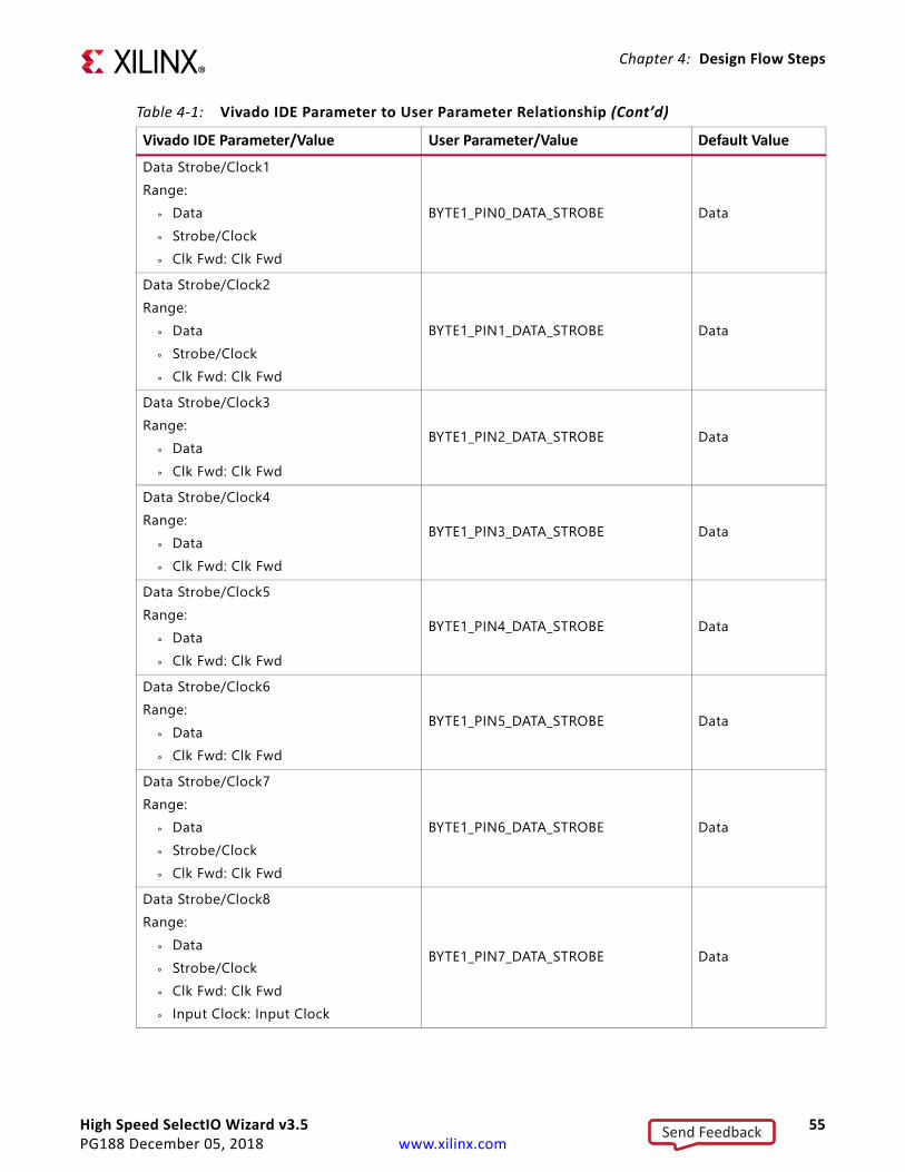
High Speed SelectIO Wizard v3.5 55PG188 December 05, 2018 www.xilinx.com
Chapter 4: Design Flow Steps
Data Strobe/Clock1Range:
° Data° Strobe/Clock° Clk Fwd: Clk Fwd
BYTE1_PIN0_DATA_STROBE Data
Data Strobe/Clock2Range:
° Data° Strobe/Clock° Clk Fwd: Clk Fwd
BYTE1_PIN1_DATA_STROBE Data
Data Strobe/Clock3Range:
° Data° Clk Fwd: Clk Fwd
BYTE1_PIN2_DATA_STROBE Data
Data Strobe/Clock4Range:
° Data° Clk Fwd: Clk Fwd
BYTE1_PIN3_DATA_STROBE Data
Data Strobe/Clock5Range:
° Data° Clk Fwd: Clk Fwd
BYTE1_PIN4_DATA_STROBE Data
Data Strobe/Clock6Range:
° Data° Clk Fwd: Clk Fwd
BYTE1_PIN5_DATA_STROBE Data
Data Strobe/Clock7Range:
° Data° Strobe/Clock° Clk Fwd: Clk Fwd
BYTE1_PIN6_DATA_STROBE Data
Data Strobe/Clock8Range:
° Data° Strobe/Clock° Clk Fwd: Clk Fwd° Input Clock: Input Clock
BYTE1_PIN7_DATA_STROBE Data
Table 4-1: Vivado IDE Parameter to User Parameter Relationship (Cont’d)
Vivado IDE Parameter/Value User Parameter/Value Default Value
Send Feedback

High Speed SelectIO Wizard v3.5 56PG188 December 05, 2018 www.xilinx.com
Chapter 4: Design Flow Steps
Data Strobe/Clock9Range:
° Data° Clk Fwd: Clk Fwd
BYTE1_PIN8_DATA_STROBE Data
Data Strobe/Clock10Range:
° Data° Clk Fwd: Clk Fwd
BYTE1_PIN9_DATA_STROBE Data
Data Strobe/Clock11Range:
° Data° Clk Fwd: Clk Fwd° Input Clock: Input Clock
BYTE1_PIN10_DATA_STROBE Data
Data Strobe/Clock12Range:
° Data° Clk Fwd: Clk Fwd
BYTE1_PIN11_DATA_STROBE Data
Data Strobe/Clock13Range:
° Data° Clk Fwd: Clk Fwd
BYTE1_PIN12_DATA_STROBE Data
Bus Sig Type1Range:
° Differential: DIFF° Single-ended: SINGLE
BYTE1_PIN0_SIG_TYPE Single-ended
Bus Sig Type2Range:
° Differential: DIFF° Single-ended: SINGLE
BYTE1_PIN1_SIG_TYPE Single-ended
Bus Sig Type3Range:
° Differential: DIFF° Single-ended: SINGLE
BYTE1_PIN2_SIG_TYPE Single-ended
Bus Sig Type4Range:
° Differential: DIFF° Single-ended: SINGLE
BYTE1_PIN3_SIG_TYPE Single-ended
Table 4-1: Vivado IDE Parameter to User Parameter Relationship (Cont’d)
Vivado IDE Parameter/Value User Parameter/Value Default Value
Send Feedback

High Speed SelectIO Wizard v3.5 57PG188 December 05, 2018 www.xilinx.com
Chapter 4: Design Flow Steps
Bus Sig Type5Range:
° Differential: DIFF° Single-ended: SINGLE
BYTE1_PIN4_SIG_TYPE Single-ended
Bus Sig Type6Range:
° Differential: DIFF° Single-ended: SINGLE
BYTE1_PIN5_SIG_TYPE Single-ended
Bus Sig Type7Range:
° Differential: DIFF° Single-ended: SINGLE
BYTE1_PIN6_SIG_TYPE Single-ended
Bus Sig Type8Range:
° Differential: DIFF° Single-ended: SINGLE
BYTE1_PIN7_SIG_TYPE Single-ended
Bus Sig Type9Range:
° Differential: DIFF° Single-ended: SINGLE
BYTE1_PIN8_SIG_TYPE Single-ended
Bus Sig Type10Range:
° Differential: DIFF° Single-ended: SINGLE
BYTE1_PIN9_SIG_TYPE Single-ended
Bus Sig Type11Range:
° Differential: DIFF° Single-ended: SINGLE
BYTE1_PIN10_SIG_TYPE Single-ended
Bus Sig Type12Range:
° Differential: DIFF° Single-ended: SINGLE
BYTE1_PIN11_SIG_TYPE Single-ended
Bus Sig Type13Range: Single-ended: SINGLE BYTE1_PIN12_SIG_TYPE Single-ended
Byte group1 Pin Selection1Range:
° TRUE° FALSE
ENABLE_BYTE1_PIN0 FALSE
Table 4-1: Vivado IDE Parameter to User Parameter Relationship (Cont’d)
Vivado IDE Parameter/Value User Parameter/Value Default Value
Send Feedback

High Speed SelectIO Wizard v3.5 58PG188 December 05, 2018 www.xilinx.com
Chapter 4: Design Flow Steps
Byte group1 Pin Selection2Range:
° TRUE° FALSE
ENABLE_BYTE1_PIN1 FALSE
Byte group1 Pin Selection3Range:
° TRUE° FALSE
ENABLE_BYTE1_PIN2 FALSE
Byte group1 Pin Selection4Range:
° TRUE° FALSE
ENABLE_BYTE1_PIN3 FALSE
Byte group1 Pin Selection5Range:
° TRUE° FALSE
ENABLE_BYTE1_PIN4 FALSE
Byte group1 Pin Selection6Range:
° TRUE° FALSE
ENABLE_BYTE1_PIN5 FALSE
Byte group1 Pin Selection7Range:
° TRUE° FALSE
ENABLE_BYTE1_PIN6 FALSE
Byte group1 Pin Selection8Range:
° TRUE° FALSE
ENABLE_BYTE1_PIN7 FALSE
Byte group1 Pin Selection9Range:
° TRUE° FALSE
ENABLE_BYTE1_PIN8 FALSE
Byte group1 Pin Selection10Range:
° TRUE° FALSE
ENABLE_BYTE1_PIN9 FALSE
Table 4-1: Vivado IDE Parameter to User Parameter Relationship (Cont’d)
Vivado IDE Parameter/Value User Parameter/Value Default Value
Send Feedback

High Speed SelectIO Wizard v3.5 59PG188 December 05, 2018 www.xilinx.com
Chapter 4: Design Flow Steps
Byte group1 Pin Selection11Range:
° TRUE° FALSE
ENABLE_BYTE1_PIN10 FALSE
Byte group1 Pin Selection12Range:
° TRUE° FALSE
ENABLE_BYTE1_PIN11 FALSE
Byte group1 Pin Selection13Range:
° TRUE° FALSE
ENABLE_BYTE1_PIN12 FALSE
Byte Group1 Signal Name1 BYTE1_PIN0_SIGNAL_NAME bg1_pin0Byte Group1 Signal Name2 BYTE1_PIN1_SIGNAL_NAME bg1_pin1Byte Group1 Signal Name3 BYTE1_PIN2_SIGNAL_NAME bg1_pin2Byte Group1 Signal Name4 BYTE1_PIN3_SIGNAL_NAME bg1_pin3Byte Group1 Signal Name5 BYTE1_PIN4_SIGNAL_NAME bg1_pin4Byte Group1 Signal Name6 BYTE1_PIN5_SIGNAL_NAME bg1_pin5Byte Group1 Signal Name7 BYTE1_PIN6_SIGNAL_NAME bg1_pin6Byte Group1 Signal Name8 BYTE1_PIN7_SIGNAL_NAME bg1_pin7Byte Group1 Signal Name9 BYTE1_PIN8_SIGNAL_NAME bg1_pin8Byte Group1 Signal Name10 BYTE1_PIN9_SIGNAL_NAME bg1_pin9Byte Group1 Signal Name11 BYTE1_PIN10_SIGNAL_NAME bg1_pin10Byte Group1 Signal Name12 BYTE1_PIN11_SIGNAL_NAME bg1_pin11Byte Group1 Signal Name13 BYTE1_PIN12_SIGNAL_NAME bg1_pin12bus dir1Range:
° TX° RX° BiDir (Beta)
BYTE2_PIN0_BUS_DIR RX
bus dir2Range:
° TX° RX° BiDir (Beta)
BYTE2_PIN1_BUS_DIR RX
Table 4-1: Vivado IDE Parameter to User Parameter Relationship (Cont’d)
Vivado IDE Parameter/Value User Parameter/Value Default Value
Send Feedback

High Speed SelectIO Wizard v3.5 60PG188 December 05, 2018 www.xilinx.com
Chapter 4: Design Flow Steps
bus dir3Range:
° TX° RX° BiDir (Beta)
BYTE2_PIN2_BUS_DIR RX
bus dir4Range:
° TX° RX° BiDir (Beta)
BYTE2_PIN3_BUS_DIR RX
bus dir5Range:
° TX° RX° BiDir (Beta)
BYTE2_PIN4_BUS_DIR RX
bus dir6Range:
° TX° RX° BiDir (Beta)
BYTE2_PIN5_BUS_DIR RX
bus dir7Range:
° TX° RX° BiDir (Beta)
BYTE2_PIN6_BUS_DIR RX
bus dir8Range:
° TX° RX° BiDir (Beta)
BYTE2_PIN7_BUS_DIR RX
bus dir9Range:
° TX° RX° BiDir (Beta)
BYTE2_PIN8_BUS_DIR RX
Table 4-1: Vivado IDE Parameter to User Parameter Relationship (Cont’d)
Vivado IDE Parameter/Value User Parameter/Value Default Value
Send Feedback
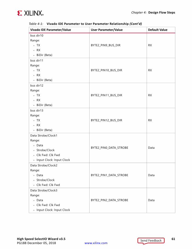
High Speed SelectIO Wizard v3.5 61PG188 December 05, 2018 www.xilinx.com
Chapter 4: Design Flow Steps
bus dir10Range:
° TX° RX° BiDir (Beta)
BYTE2_PIN9_BUS_DIR RX
bus dir11Range:
° TX° RX° BiDir (Beta)
BYTE2_PIN10_BUS_DIR RX
bus dir12Range:
° TX° RX° BiDir (Beta)
BYTE2_PIN11_BUS_DIR RX
bus dir13Range:
° TX° RX° BiDir (Beta)
BYTE2_PIN12_BUS_DIR RX
Data Strobe/Clock1Range:
° Data° Strobe/Clock° Clk Fwd: Clk Fwd° Input Clock: Input Clock
BYTE2_PIN0_DATA_STROBE Data
Data Strobe/Clock2Range:
° Data° Strobe/Clock° Clk Fwd: Clk Fwd
BYTE2_PIN1_DATA_STROBE Data
Data Strobe/Clock3Range:
° Data° Clk Fwd: Clk Fwd° Input Clock: Input Clock
BYTE2_PIN2_DATA_STROBE Data
Table 4-1: Vivado IDE Parameter to User Parameter Relationship (Cont’d)
Vivado IDE Parameter/Value User Parameter/Value Default Value
Send Feedback

High Speed SelectIO Wizard v3.5 62PG188 December 05, 2018 www.xilinx.com
Chapter 4: Design Flow Steps
Data Strobe/Clock4Range:
° Data° Clk Fwd: Clk Fwd
BYTE2_PIN3_DATA_STROBE Data
Data Strobe/Clock5Range:
° Data° Clk Fwd: Clk Fwd
BYTE2_PIN4_DATA_STROBE Data
Data Strobe/Clock6Range:
° Data° Clk Fwd: Clk Fwd
BYTE2_PIN5_DATA_STROBE Data
Data Strobe/Clock7Range:
° Data° Strobe/Clock° Clk Fwd: Clk Fwd
BYTE2_PIN6_DATA_STROBE Data
Data Strobe/Clock8Range:
° Data° Strobe/Clock° Clk Fwd: Clk Fwd
BYTE2_PIN7_DATA_STROBE Data
Data Strobe/Clock9Range:
° Data° Clk Fwd: Clk Fwd
BYTE2_PIN8_DATA_STROBE Data
Data Strobe/Clock10Range:
° Data° Clk Fwd: Clk Fwd
BYTE2_PIN9_DATA_STROBE Data
Data Strobe/Clock11Range:
° Data° Clk Fwd: Clk Fwd
BYTE2_PIN10_DATA_STROBE Data
Data Strobe/Clock12Range:
° Data° Clk Fwd: Clk Fwd
BYTE2_PIN11_DATA_STROBE Data
Table 4-1: Vivado IDE Parameter to User Parameter Relationship (Cont’d)
Vivado IDE Parameter/Value User Parameter/Value Default Value
Send Feedback
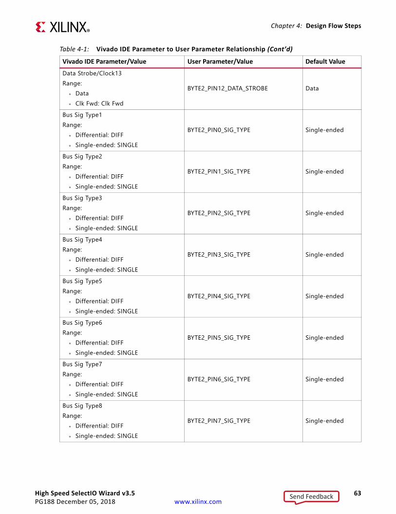
High Speed SelectIO Wizard v3.5 63PG188 December 05, 2018 www.xilinx.com
Chapter 4: Design Flow Steps
Data Strobe/Clock13Range:
° Data° Clk Fwd: Clk Fwd
BYTE2_PIN12_DATA_STROBE Data
Bus Sig Type1Range:
° Differential: DIFF° Single-ended: SINGLE
BYTE2_PIN0_SIG_TYPE Single-ended
Bus Sig Type2Range:
° Differential: DIFF° Single-ended: SINGLE
BYTE2_PIN1_SIG_TYPE Single-ended
Bus Sig Type3Range:
° Differential: DIFF° Single-ended: SINGLE
BYTE2_PIN2_SIG_TYPE Single-ended
Bus Sig Type4Range:
° Differential: DIFF° Single-ended: SINGLE
BYTE2_PIN3_SIG_TYPE Single-ended
Bus Sig Type5Range:
° Differential: DIFF° Single-ended: SINGLE
BYTE2_PIN4_SIG_TYPE Single-ended
Bus Sig Type6Range:
° Differential: DIFF° Single-ended: SINGLE
BYTE2_PIN5_SIG_TYPE Single-ended
Bus Sig Type7Range:
° Differential: DIFF° Single-ended: SINGLE
BYTE2_PIN6_SIG_TYPE Single-ended
Bus Sig Type8Range:
° Differential: DIFF° Single-ended: SINGLE
BYTE2_PIN7_SIG_TYPE Single-ended
Table 4-1: Vivado IDE Parameter to User Parameter Relationship (Cont’d)
Vivado IDE Parameter/Value User Parameter/Value Default Value
Send Feedback

High Speed SelectIO Wizard v3.5 64PG188 December 05, 2018 www.xilinx.com
Chapter 4: Design Flow Steps
Bus Sig Type9Range:
° Differential: DIFF° Single-ended: SINGLE
BYTE2_PIN8_SIG_TYPE Single-ended
Bus Sig Type10Range:
° Differential: DIFF° Single-ended: SINGLE
BYTE2_PIN9_SIG_TYPE Single-ended
Bus Sig Type11Range:
° Differential: DIFF° Single-ended: SINGLE
BYTE2_PIN10_SIG_TYPE Single-ended
Bus Sig Type12Range:
° Differential: DIFF° Single-ended: SINGLE
BYTE2_PIN11_SIG_TYPE Single-ended
Bus Sig Type13Range: Single-ended: SINGLE BYTE2_PIN12_SIG_TYPE Single-ended
Byte group2 Pin Selection1Range:
° TRUE° FALSE
ENABLE_BYTE2_PIN0 FALSE
Byte group2 Pin Selection2Range:
° TRUE° FALSE
ENABLE_BYTE2_PIN1 FALSE
Byte group2 Pin Selection3Range:
° TRUE° FALSE
ENABLE_BYTE2_PIN2 FALSE
Byte group2 Pin Selection4Range:
° TRUE° FALSE
ENABLE_BYTE2_PIN3 FALSE
Byte group2 Pin Selection5Range:
° TRUE° FALSE
ENABLE_BYTE2_PIN4 FALSE
Table 4-1: Vivado IDE Parameter to User Parameter Relationship (Cont’d)
Vivado IDE Parameter/Value User Parameter/Value Default Value
Send Feedback
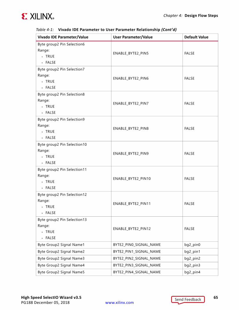
High Speed SelectIO Wizard v3.5 65PG188 December 05, 2018 www.xilinx.com
Chapter 4: Design Flow Steps
Byte group2 Pin Selection6Range:
° TRUE° FALSE
ENABLE_BYTE2_PIN5 FALSE
Byte group2 Pin Selection7Range:
° TRUE° FALSE
ENABLE_BYTE2_PIN6 FALSE
Byte group2 Pin Selection8Range:
° TRUE° FALSE
ENABLE_BYTE2_PIN7 FALSE
Byte group2 Pin Selection9Range:
° TRUE° FALSE
ENABLE_BYTE2_PIN8 FALSE
Byte group2 Pin Selection10Range:
° TRUE° FALSE
ENABLE_BYTE2_PIN9 FALSE
Byte group2 Pin Selection11Range:
° TRUE° FALSE
ENABLE_BYTE2_PIN10 FALSE
Byte group2 Pin Selection12Range:
° TRUE° FALSE
ENABLE_BYTE2_PIN11 FALSE
Byte group2 Pin Selection13Range:
° TRUE° FALSE
ENABLE_BYTE2_PIN12 FALSE
Byte Group2 Signal Name1 BYTE2_PIN0_SIGNAL_NAME bg2_pin0Byte Group2 Signal Name2 BYTE2_PIN1_SIGNAL_NAME bg2_pin1Byte Group2 Signal Name3 BYTE2_PIN2_SIGNAL_NAME bg2_pin2Byte Group2 Signal Name4 BYTE2_PIN3_SIGNAL_NAME bg2_pin3Byte Group2 Signal Name5 BYTE2_PIN4_SIGNAL_NAME bg2_pin4
Table 4-1: Vivado IDE Parameter to User Parameter Relationship (Cont’d)
Vivado IDE Parameter/Value User Parameter/Value Default Value
Send Feedback
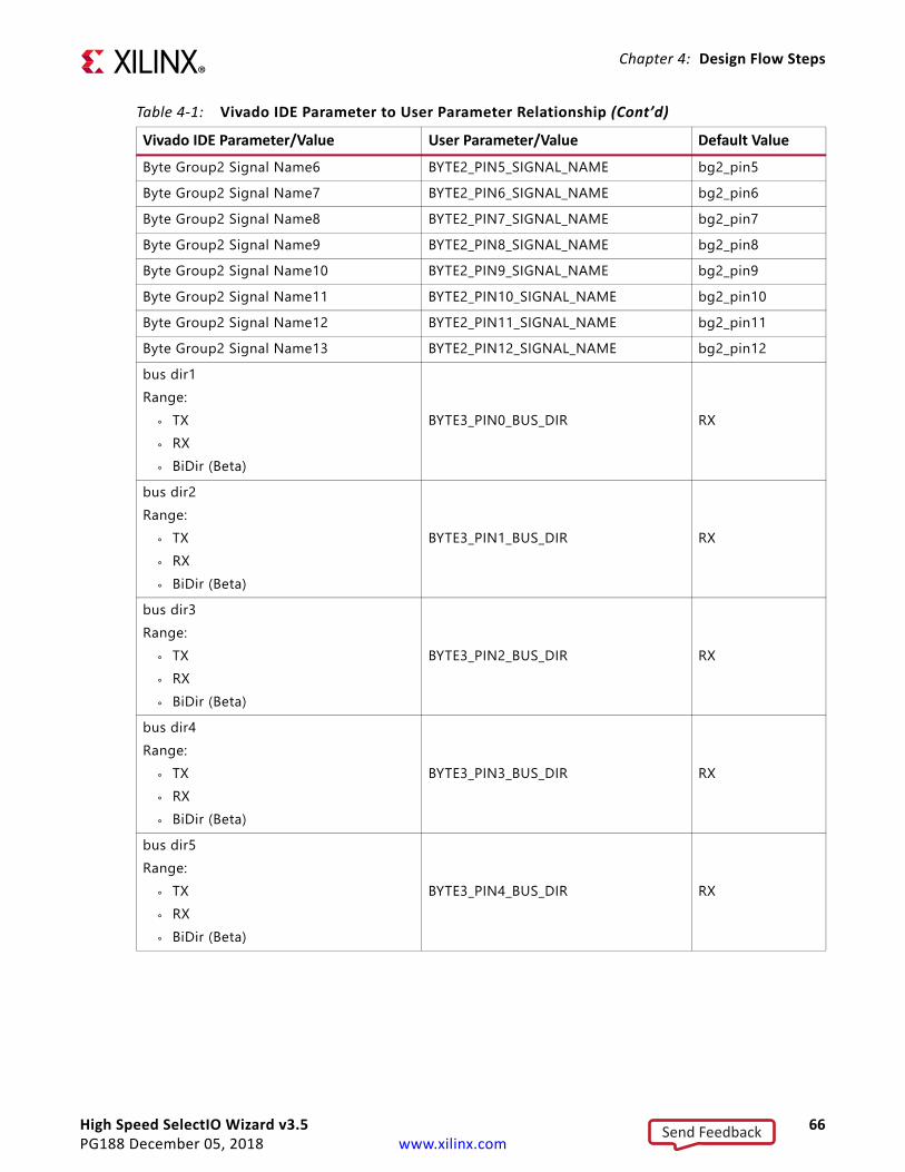
High Speed SelectIO Wizard v3.5 66PG188 December 05, 2018 www.xilinx.com
Chapter 4: Design Flow Steps
Byte Group2 Signal Name6 BYTE2_PIN5_SIGNAL_NAME bg2_pin5Byte Group2 Signal Name7 BYTE2_PIN6_SIGNAL_NAME bg2_pin6Byte Group2 Signal Name8 BYTE2_PIN7_SIGNAL_NAME bg2_pin7Byte Group2 Signal Name9 BYTE2_PIN8_SIGNAL_NAME bg2_pin8Byte Group2 Signal Name10 BYTE2_PIN9_SIGNAL_NAME bg2_pin9Byte Group2 Signal Name11 BYTE2_PIN10_SIGNAL_NAME bg2_pin10Byte Group2 Signal Name12 BYTE2_PIN11_SIGNAL_NAME bg2_pin11Byte Group2 Signal Name13 BYTE2_PIN12_SIGNAL_NAME bg2_pin12bus dir1Range:
° TX° RX° BiDir (Beta)
BYTE3_PIN0_BUS_DIR RX
bus dir2Range:
° TX° RX° BiDir (Beta)
BYTE3_PIN1_BUS_DIR RX
bus dir3Range:
° TX° RX° BiDir (Beta)
BYTE3_PIN2_BUS_DIR RX
bus dir4Range:
° TX° RX° BiDir (Beta)
BYTE3_PIN3_BUS_DIR RX
bus dir5Range:
° TX° RX° BiDir (Beta)
BYTE3_PIN4_BUS_DIR RX
Table 4-1: Vivado IDE Parameter to User Parameter Relationship (Cont’d)
Vivado IDE Parameter/Value User Parameter/Value Default Value
Send Feedback

High Speed SelectIO Wizard v3.5 67PG188 December 05, 2018 www.xilinx.com
Chapter 4: Design Flow Steps
bus dir6Range:
° TX° RX° BiDir (Beta)
BYTE3_PIN5_BUS_DIR RX
bus dir7Range:
° TX° RX° BiDir (Beta)
BYTE3_PIN6_BUS_DIR RX
bus dir8Range:
° TX° RX° BiDir (Beta)
BYTE3_PIN7_BUS_DIR RX
bus dir9Range:
° TX° RX° BiDir (Beta)
BYTE3_PIN8_BUS_DIR RX
bus dir10Range:
° TX° RX° BiDir (Beta)
BYTE3_PIN9_BUS_DIR RX
bus dir11Range:
° TX° RX° BiDir (Beta)
BYTE3_PIN10_BUS_DIR RX
bus dir12Range:
° TX° RX° BiDir (Beta)
BYTE3_PIN11_BUS_DIR RX
Table 4-1: Vivado IDE Parameter to User Parameter Relationship (Cont’d)
Vivado IDE Parameter/Value User Parameter/Value Default Value
Send Feedback

High Speed SelectIO Wizard v3.5 68PG188 December 05, 2018 www.xilinx.com
Chapter 4: Design Flow Steps
bus dir13Range:
° TX° RX° BiDir (Beta)
BYTE3_PIN12_BUS_DIR RX
Data Strobe/Clock1Range:
° Data° Strobe/Clock° Clk Fwd: Clk Fwd
BYTE3_PIN0_DATA_STROBE Data
Data Strobe/Clock2Range:
° Data° Strobe/Clock° Clk Fwd: Clk Fwd
BYTE3_PIN1_DATA_STROBE Data
Data Strobe/Clock3Range:
° Data° Clk Fwd: Clk Fwd
BYTE3_PIN2_DATA_STROBE Data
Data Strobe/Clock4Range:
° Data° Clk Fwd: Clk Fwd
BYTE3_PIN3_DATA_STROBE Data
Data Strobe/Clock5Range:
° Data° Clk Fwd: Clk Fwd
BYTE3_PIN4_DATA_STROBE Data
Data Strobe/Clock6Range:
° Data° Clk Fwd: Clk Fwd
BYTE3_PIN5_DATA_STROBE Data
Data Strobe/Clock7Range:
° Data° Strobe/Clock° Clk Fwd: Clk Fwd
BYTE3_PIN6_DATA_STROBE Data
Table 4-1: Vivado IDE Parameter to User Parameter Relationship (Cont’d)
Vivado IDE Parameter/Value User Parameter/Value Default Value
Send Feedback

High Speed SelectIO Wizard v3.5 69PG188 December 05, 2018 www.xilinx.com
Chapter 4: Design Flow Steps
Data Strobe/Clock8Range:
° Data° Strobe/Clock° Clk Fwd: Clk Fwd
BYTE3_PIN7_DATA_STROBE Data
Data Strobe/Clock9Range:
° Data° Clk Fwd: Clk Fwd
BYTE3_PIN8_DATA_STROBE Data
Data Strobe/Clock10Range:
° Data° Clk Fwd: Clk Fwd
BYTE3_PIN9_DATA_STROBE Data
Data Strobe/Clock11Range:
° Data° Clk Fwd: Clk Fwd
BYTE3_PIN10_DATA_STROBE Data
Data Strobe/Clock12Range:
° Data° Clk Fwd: Clk Fwd
BYTE3_PIN11_DATA_STROBE Data
Data Strobe/Clock13Range:
° Data° Clk Fwd: Clk Fwd
BYTE3_PIN12_DATA_STROBE Data
Bus Sig Type1Range:
° Differential: DIFF° Single-ended: SINGLE
BYTE3_PIN0_SIG_TYPE Single-ended
Bus Sig Type2Range:
° Differential: DIFF° Single-ended: SINGLE
BYTE3_PIN1_SIG_TYPE Single-ended
Bus Sig Type3Range:
° Differential: DIFF° Single-ended: SINGLE
BYTE3_PIN2_SIG_TYPE Single-ended
Table 4-1: Vivado IDE Parameter to User Parameter Relationship (Cont’d)
Vivado IDE Parameter/Value User Parameter/Value Default Value
Send Feedback
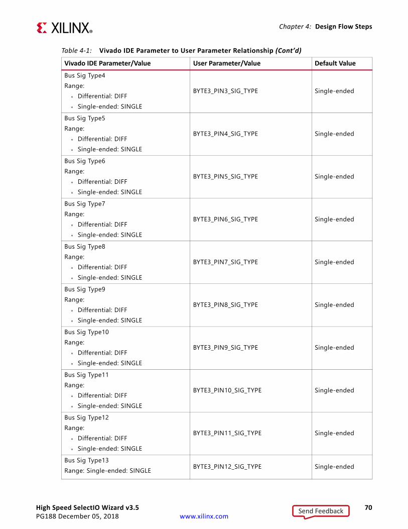
High Speed SelectIO Wizard v3.5 70PG188 December 05, 2018 www.xilinx.com
Chapter 4: Design Flow Steps
Bus Sig Type4Range:
° Differential: DIFF° Single-ended: SINGLE
BYTE3_PIN3_SIG_TYPE Single-ended
Bus Sig Type5Range:
° Differential: DIFF° Single-ended: SINGLE
BYTE3_PIN4_SIG_TYPE Single-ended
Bus Sig Type6Range:
° Differential: DIFF° Single-ended: SINGLE
BYTE3_PIN5_SIG_TYPE Single-ended
Bus Sig Type7Range:
° Differential: DIFF° Single-ended: SINGLE
BYTE3_PIN6_SIG_TYPE Single-ended
Bus Sig Type8Range:
° Differential: DIFF° Single-ended: SINGLE
BYTE3_PIN7_SIG_TYPE Single-ended
Bus Sig Type9Range:
° Differential: DIFF° Single-ended: SINGLE
BYTE3_PIN8_SIG_TYPE Single-ended
Bus Sig Type10Range:
° Differential: DIFF° Single-ended: SINGLE
BYTE3_PIN9_SIG_TYPE Single-ended
Bus Sig Type11Range:
° Differential: DIFF° Single-ended: SINGLE
BYTE3_PIN10_SIG_TYPE Single-ended
Bus Sig Type12Range:
° Differential: DIFF° Single-ended: SINGLE
BYTE3_PIN11_SIG_TYPE Single-ended
Bus Sig Type13Range: Single-ended: SINGLE BYTE3_PIN12_SIG_TYPE Single-ended
Table 4-1: Vivado IDE Parameter to User Parameter Relationship (Cont’d)
Vivado IDE Parameter/Value User Parameter/Value Default Value
Send Feedback

High Speed SelectIO Wizard v3.5 71PG188 December 05, 2018 www.xilinx.com
Chapter 4: Design Flow Steps
Byte group3 Pin Selection1Range:
° TRUE° FALSE
ENABLE_BYTE3_PIN0 FALSE
Byte group3 Pin Selection2Range:
° TRUE° FALSE
ENABLE_BYTE3_PIN1 FALSE
Byte group3 Pin Selection3Range:
° TRUE° FALSE
ENABLE_BYTE3_PIN2 FALSE
Byte group3 Pin Selection4Range:
° TRUE° FALSE
ENABLE_BYTE3_PIN3 FALSE
Byte group3 Pin Selection5Range:
° TRUE° FALSE
ENABLE_BYTE3_PIN4 FALSE
Byte group3 Pin Selection6Range:
° TRUE° FALSE
ENABLE_BYTE3_PIN5 FALSE
Byte group3 Pin Selection7Range:
° TRUE° FALSE
ENABLE_BYTE3_PIN6 FALSE
Byte group3 Pin Selection8Range:
° TRUE° FALSE
ENABLE_BYTE3_PIN7 FALSE
Byte group3 Pin Selection9Range:
° TRUE° FALSE
ENABLE_BYTE3_PIN8 FALSE
Table 4-1: Vivado IDE Parameter to User Parameter Relationship (Cont’d)
Vivado IDE Parameter/Value User Parameter/Value Default Value
Send Feedback

High Speed SelectIO Wizard v3.5 72PG188 December 05, 2018 www.xilinx.com
Chapter 4: Design Flow Steps
Byte group3 Pin Selection10Range:
° TRUE° FALSE
ENABLE_BYTE3_PIN9 FALSE
Byte group3 Pin Selection11Range:
° TRUE° FALSE
ENABLE_BYTE3_PIN10 FALSE
Byte group3 Pin Selection12Range:
° TRUE° FALSE
ENABLE_BYTE3_PIN11 FALSE
Byte group3 Pin Selection13Range:
° TRUE° FALSE
ENABLE_BYTE3_PIN12 FALSE
Byte Group3 Signal Name1 BYTE3_PIN0_SIGNAL_NAME bg3_pin0Byte Group3 Signal Name2 BYTE3_PIN1_SIGNAL_NAME bg3_pin1Byte Group3 Signal Name3 BYTE3_PIN2_SIGNAL_NAME bg3_pin2Byte Group3 Signal Name4 BYTE3_PIN3_SIGNAL_NAME bg3_pin3Byte Group3 Signal Name5 BYTE3_PIN4_SIGNAL_NAME bg3_pin4Byte Group3 Signal Name6 BYTE3_PIN5_SIGNAL_NAME bg3_pin5Byte Group3 Signal Name7 BYTE3_PIN6_SIGNAL_NAME bg3_pin6Byte Group3 Signal Name8 BYTE3_PIN7_SIGNAL_NAME bg3_pin7Byte Group3 Signal Name9 BYTE3_PIN8_SIGNAL_NAME bg3_pin8Byte Group3 Signal Name10 BYTE3_PIN9_SIGNAL_NAME bg3_pin9Byte Group3 Signal Name11 BYTE3_PIN10_SIGNAL_NAME bg3_pin10Byte Group3 Signal Name12 BYTE3_PIN11_SIGNAL_NAME bg3_pin11Byte Group3 Signal Name13 BYTE3_PIN12_SIGNAL_NAME bg3_pin12INIT VAL1 to INIT VAL52Range:
° 0° 1
INIT_VAL 0
Table 4-1: Vivado IDE Parameter to User Parameter Relationship (Cont’d)
Vivado IDE Parameter/Value User Parameter/Value Default Value
Send Feedback

High Speed SelectIO Wizard v3.5 73PG188 December 05, 2018 www.xilinx.com
Chapter 4: Design Flow Steps
Output GenerationThe core delivers Verilog RTL for the core logic, example design, and example test bench.
The following files are created when core is configured and output products are generated:
<ComponentName>.v - Top Level wrapper to be instantiated in User Design
- <ComponentName>_high_speed_selectio_wiz_v3_0.v - Top Level file to set the appropriate HDL parameters for a given configuration
- hssio_wiz_top.v - Top level file
- bs_top.v - Top level file for Bitslice and Bitslice Control Modules
- rxtx_bs.v - Instantiates RXTX_BITSLICE module
- tx_bs_tri.v - Instantiates TX_BITSLICE_TRI module
- tx_bs.v - Instantiates TX_BITSLICE module
- rx_bs.v - Instantiate RX_BITSLICE module
- BitSlipInLogic_Toplevel.v (Optional Module for BitSlip Operation)
- C2BCEtc.v
- C2BCEtc_dwnld.v
- C3BCEtc.v
- C3BCEtc_dwnld.v
- Fdcr.v
- GenPulse.v
- BitSlipInLogic_4b.v
- BitSlipInLogic_8b.v
- BitSlipInLogic_FstCmp_4b.v
- BitSlipInLogic_FstCmp_8b.v
- clk_rst_top.v - Instantiates Clock and Reset Modules
- rst_scheme.v - Reset Logic
Send Feedback

High Speed SelectIO Wizard v3.5 74PG188 December 05, 2018 www.xilinx.com
Chapter 4: Design Flow Steps
- clk_scheme.v - Clocking Logic - Instantiates PLL
- bs_ctrl_top.v - Instantiates BITSLICE_CONTROL module
- iobuf_top.v - Instantiates I/O Buffers for all Clock and Data Pins
If the IP example design project is opened, another core instance with the core name <ip_ex_inst> is instantiated in the <ComponentName>_exdes.v. For example design simulation, the <ComponentName>_tb.v test bench file is generated.
Constraining the CoreThis section contains information about constraining the core in the Vivado Design Suite.
Required ConstraintsRefer to the I/O Standard in Configuration Settings — Basic.
Device, Package, and Speed Grade SelectionsInput clock frequency selection depends on the maximum frequencies supported by the BUFG. Select the device, package and speed grades after referring to the following data sheets for details on supported maximum frequencies.
• Kintex UltraScale Architecture Data Sheet (DS892) [Ref 2] • Virtex UltraScale FPGAs Data Sheet (DS893) [Ref 3]• Kintex UltraScale+ FPGAs Data Sheet (DS922) [Ref 4]
Clock FrequenciesThe I/O logic for this core works in the range 300-800 Mb/s. The general interconnect logic for this core works up to 200 Mb/s.
If timing issues are seen for signals driving inputs to XiPHY, refer to Xilinx Answer 67104 for details on constraining the PLL clock,
Clock ManagementAll clocks are generated using PLL.
IMPORTANT: Core logic should be clocked with the divided version of the PLL output.
Send Feedback

High Speed SelectIO Wizard v3.5 75PG188 December 05, 2018 www.xilinx.com
Chapter 4: Design Flow Steps
Clock PlacementThe input clock can be placed on global clock pins with the name *_GC_*. For EDGE DDR/CENTER DDR, the clock is placed on *_GC_QBC* pin only.
BankingThis core can be used to configure an I/O circuit for High Range (HR) and High Performance (HP) banks. Available banks for the project part are provided in the Vivado IDE for selection. See Customizing and Generating the Core for more details.
Transceiver PlacementThere are no transceiver placement constraints for this core.
I/O Standard and PlacementNote: The wizard can infer some bitslices for strobe propagation in the RX and BiDir (Beta) bus configuration; these are displayed under the comment.
############# I/O constraints for wizard inferred RX bitslice #######################
For these bitslices, only the single-ended I/O standard is applicable. In case only differential pins are selected during configuration, ensure that the appropriate single ended I/O standard is set in the XDC file for inferred RX bit slice.
Refer to UltraScale Architecture SelectIO Resources: Advance Specification User Guide (UG571) [Ref 1] for the supported I/O standards.
SimulationFor comprehensive information about Vivado simulation components, as well as information about using supported third-party tools, see the Vivado Design Suite User Guide: Logic Simulation (UG900) [Ref 8].
Synthesis and ImplementationFor details about synthesis and implementation, see the Vivado Design Suite User Guide: Designing with IP (UG896) [Ref 6].
Send Feedback

High Speed SelectIO Wizard v3.5 76PG188 December 05, 2018 www.xilinx.com
Chapter 5
Example DesignThis chapter contains information about the example design provided in the Vivado® Design Suite.
This core provides an example design with one core instance and one example instance. For each configured pin of the IP instance, a counterpart (example design) is generated. When bitslip is enabled, the pre-defined training pattern is compared to align the data at RX. When data is aligned, PRBS patterns are transmitted from Tx and PRBS checkers at the Rx (in the example instance) check for data integrity. When bitslip is not enabled, data from RX bitslices are unaligned data, and the example design checks for all possible valid data of RX for a known TX data pattern. If a pattern matches, data_check_complete output is asserted from the example design.X-Ref Target - Figure 5-1
Figure 5-1: Example Design Block Diagram
Send Feedback

High Speed SelectIO Wizard v3.5 77PG188 December 05, 2018 www.xilinx.com
Chapter 5: Example Design
Table 5-1: DUT and Partner IP ConfigurationsDUT Configuration Partner IP Configuration
TX with no Clock Forward PinRX in Serial Mode. Simulation is not guaranteed to pass in this configuration because Rx being in serial mode does not have data capture logic in the example design.
TX with Clock Forward Pin and Clock Forward Phase= 0 RX in Edge DDR mode
TX with Clock Forward Pin and Clock Forward Phase= 90 RX in Center DDR mode
RX – Edge DDR/ Center DDR TX with Clock Forward Pin
RX – Edge DDR Strobe TX with Clock Forward Pin and Clock Forward Phase = 0
RX – Center DDR Strobe TX with Clock Forward Pin and Clock Forward Phase = 90
Mix of TX, RX and BiDir (Beta) Supported only for the configurations given below.TX with no clock forward pin and interface speed less than 600 Mb/s Not supported
Table 5-2: Configuration of DUT Supported in Example Design for Mix of TX, RX and BiDir (Beta) PinsMode Max TX/BIDIR Pins Max RX/BIDIR Pins Comments
TX + RXBIDIR + TX orBIDIR + RX
26 26 Split at byte groupboundary in partner
39 13 Split at byte groupboundary in partner
13 39 Split at byte groupboundary in partner
Table 5-3: Configuration of DUT Supported in Example Design for TX, RX and BiDir Pins
Mode Max TX Pins Max RX Pins Max BIDIR Pins Comments
TX + RX +BIDIR
26 13 13 Split at byte groupboundary in partner
13 13 26 Split at byte groupboundary in partner
13 26 13 Split at byte groupboundary in partner
Send Feedback

High Speed SelectIO Wizard v3.5 78PG188 December 05, 2018 www.xilinx.com
Chapter 6
Test BenchThis chapter contains information about the test bench provided in the Vivado® Design Suite. The test bench is a simple Verilog code to exercise the example design and the core. This test bench performs the following tasks:
• Generates the input clock signals.• Applies a reset to the example design.• Example design RX and TX interfaces are looped back; similarly IP BiDir (Beta) bus and
example design BIDIR buses are looped back. The waveform is shown for the TX/RX loopback for 1 pin.
• If an RX and TX pattern matches, the test bench sends a message for the successful test completion, as shown in Figure 6-1. Otherwise, it waits for 16,000 cycles of input clock and sends a test failure message.
• Checks the alignment of data on the TX pin for source synchronous interfaces.X-Ref Target - Figure 6-1
Figure 6-1: Test Bench Waveform X18791-021617
Send Feedback

High Speed SelectIO Wizard v3.5 79PG188 December 05, 2018 www.xilinx.com
Appendix A
Verification, Compliance, and Interoperability
This appendix provides details about how this IP core was tested for compliance with the protocol to which it was designed.
SimulationThis core is verified with incisive enterprise simulator (IES), Verilog compiled simulator (VCS), Mentor Graphics Questa Advanced Simulator, and XSIM simulators.
Hardware TestingHardware testing was performed on the KCU105 platform for the RX and TX configurations using the MicroBlaze™ processor system to generate the data pattern for the TX and check the data at the RX. The TX and RX pins were connected to an FMC 107 loopback card placed on an HPC connector onboard. Tests were performed on the supported data speed range.
Send Feedback

High Speed SelectIO Wizard v3.5 80PG188 December 05, 2018 www.xilinx.com
Appendix B
UpgradingMigrating and upgrading the core is supported from the v3.0 version of the core. Upgrade is not supported from versions earlier to v3.0 Refer to Xilinx Answer 64216 for guidance on upgrading the core from the previous version.
Upgrading in the Vivado Design SuiteThis section provides information about any changes to the user logic or port designations between core versions.
Changes from v3.1 to v3.2
Ports Added
• clock_from_ibuf• app_clk• intf_rdy• multi_intf_lock_in
Other Changes
Updated the clock domains from pll0_clkout0 to pll0_clkout0 or app_clk for the following ports.
• data_from_fabric_<sig_name>_<y> [sf -1:0]• data_ti_fabric_<sig_name>_<y> [sf -1:0]• tri_tbyte<n>[3:0]• tri_t<i>• fifo_empty_<i>• fifo_rd_en_<i>• fifo_rd_clk_<i>
Send Feedback

High Speed SelectIO Wizard v3.5 81PG188 December 05, 2018 www.xilinx.com
Appendix C
DebuggingThis appendix includes details about resources available on the Xilinx Support website and debugging tools.
Finding Help on Xilinx.comTo help in the design and debug process when using the High Speed SelectIO Wizard, the Xilinx Support web page contains key resources such as product documentation, release notes, answer records, information about known issues, and links for obtaining further product support.
DocumentationThis product guide is the main document associated with the High Speed SelectIO Wizard. This guide, along with documentation related to all products that aid in the design process, can be found on the Xilinx Support web page or by using the Xilinx® Documentation Navigator.
Download the Xilinx Documentation Navigator from the Downloads page. For more information about this tool and the features available, open the online help after installation.
Answer Records Answer Records include information about commonly encountered problems, helpful information on how to resolve these problems, and any known issues with a Xilinx product. Answer Records are created and maintained daily ensuring that users have access to the most accurate information available.
Answer Records for this core can be located by using the Search Support box on the main Xilinx support web page. To maximize your search results, use proper keywords such as
• Product name• Tool message(s)• Summary of the issue encountered
Send Feedback

High Speed SelectIO Wizard v3.5 82PG188 December 05, 2018 www.xilinx.com
Appendix C: Debugging
See Xilinx Answer: 64216
Technical SupportXilinx provides technical support in the Xilinx Support web page for this LogiCORE™ IP product when used as described in the product documentation. Xilinx cannot guarantee timing, functionality, or support if you do any of the following:
• Implement the solution in devices that are not defined in the documentation.• Customize the solution beyond that allowed in the product documentation. • Change any section of the design labeled DO NOT MODIFY.
To contact Xilinx Technical Support, navigate to the Xilinx Support web page.
Vivado Design Suite Debug FeatureThe Vivado® Design Suite debug feature inserts logic analyzer and virtual I/O cores directly into your design. The debug feature also allows you to set trigger conditions to capture application and integrated block port signals in hardware. Captured signals can then be analyzed. This feature in the Vivado IDE is used for logic debugging and validation of a design running in Xilinx.
The Vivado logic analyzer is used with the logic debug IP cores, including:
• integrated logic analyzer (ILA) 2.0 (and later versions)• virtual input output (VIO) 2.0 (and later versions)
See the Vivado Design Suite User Guide: Programming and Debugging (UG908) [Ref 10].
Reference BoardsVarious Xilinx development boards support the High Speed SelectIO Wizard. These boards can be used to prototype designs and establish that the core can communicate with the system. The UltraScale™ architecture evaluation board KCU105 is supported.
Send Feedback

High Speed SelectIO Wizard v3.5 83PG188 December 05, 2018 www.xilinx.com
Appendix C: Debugging
Hardware DebugHardware issues can range from link bring-up to problems seen after hours of testing. This section provides debug steps for common issues. The debug feature is a valuable resource to use in hardware debug. The signal names mentioned in the following individual sections can be probed using the Vivado debug feature for debugging the specific problems.
Ensure that all the timing constraints for the core were properly incorporated from the example design and that all constraints were met during implementation.
• Does it work in post-place and route timing simulation? If problems are seen in hardware but not in timing simulation, this might indicate a PCB issue. Ensure that all clock sources are active and clean.
• Ensure that the rst_seq_done is asserted by the wizard.• Does the rst_seq_done signal toggle without the assertion of reset? If yes, this
indicates a loss of PLL lock or deassertion of the DLY_RDY and VTC_RDY signals. • Ensure that the PLL Lock signal is asserted.• Ensure that the VTC_RDY and DLY_RDY signals are asserted for all BITSLICE and
BITSLICE_CONTROL signals.• Ensure that the synthesis and implementation of the design is successful without any
DRC errors.• Check that RIU Clock is always present in the system during the deassertion of reset.• Check the status of FIFO_EMPTY signals.• If Bitslip logic is enabled, ensure that start_bitslip is driven Low whenever the
top-level rst pin is asserted.• If Bitslip logic is enabled, ensure that start_bitslip is asserted after the TX side is
transmitting.• Ensure PLL reset requirements are met.
Send Feedback

High Speed SelectIO Wizard v3.5 84PG188 December 05, 2018 www.xilinx.com
Appendix D
Additional Resources and Legal Notices
Xilinx ResourcesFor support resources such as Answers, Documentation, Downloads, and Forums, see Xilinx Support.
Documentation Navigator and Design HubsXilinx® Documentation Navigator provides access to Xilinx documents, videos, and support resources, which you can filter and search to find information. To open the Xilinx Documentation Navigator (DocNav):
• From the Vivado® IDE, select Help > Documentation and Tutorials.• On Windows, select Start > All Programs > Xilinx Design Tools > DocNav.• At the Linux command prompt, enter docnav.
Xilinx Design Hubs provide links to documentation organized by design tasks and other topics, which you can use to learn key concepts and address frequently asked questions. To access the Design Hubs:
• In the Xilinx Documentation Navigator, click the Design Hubs View tab.• On the Xilinx website, see the Design Hubs page.Note: For more information on Documentation Navigator, see the Documentation Navigator page on the Xilinx website.
Send Feedback

High Speed SelectIO Wizard v3.5 85PG188 December 05, 2018 www.xilinx.com
Appendix D: Additional Resources and Legal Notices
ReferencesThese documents provide supplemental material useful with this product guide:
1. UltraScale Architecture SelectIO Resources: Advance Specification User Guide (UG571)2. Kintex UltraScale Architecture Data Sheet (DS892)3. Virtex UltraScale FPGAs Data Sheet (DS893)4. Kintex UltraScale+ FPGAs Data Sheet (DS922)5. Vivado Design Suite User Guide: Designing IP Subsystems using IP Integrator (UG994)6. Vivado Design Suite User Guide: Designing with IP (UG896)7. Vivado Design Suite User Guide: Getting Started (UG910)8. Vivado Design Suite User Guide: Logic Simulation (UG900)9. Bitslip in Logic Application Note (XAPP1208)10. Vivado Design Suite User Guide: Programming and Debugging (UG908)11. Vivado Design Suite User Guide - Implementation (UG904)12. Native High-Speed I/O Interfaces (XAPP1274)13. UltraScale Architecture Clocking Resources User Guide (UG572)14. Vivado Design Suite: User Guide Design Analysis and Closure Techniques (UG906)15. Native High-Speed I/O Interfaces Application Note (XAPP1274)
Send Feedback
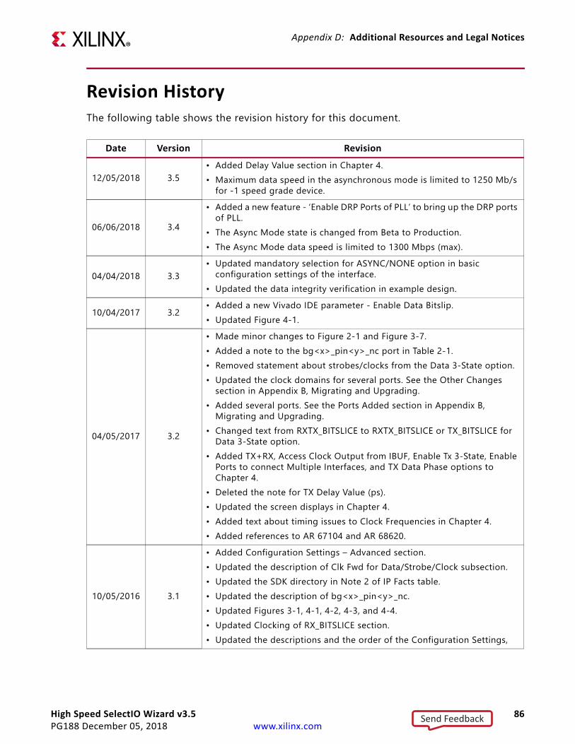
High Speed SelectIO Wizard v3.5 86PG188 December 05, 2018 www.xilinx.com
Appendix D: Additional Resources and Legal Notices
Revision HistoryThe following table shows the revision history for this document.
Date Version Revision
12/05/2018 3.5• Added Delay Value section in Chapter 4.• Maximum data speed in the asynchronous mode is limited to 1250 Mb/s
for -1 speed grade device.
06/06/2018 3.4
• Added a new feature - ‘Enable DRP Ports of PLL’ to bring up the DRP ports of PLL.
• The Async Mode state is changed from Beta to Production.• The Async Mode data speed is limited to 1300 Mbps (max).
04/04/2018 3.3• Updated mandatory selection for ASYNC/NONE option in basic
configuration settings of the interface.• Updated the data integrity verification in example design.
10/04/2017 3.2 • Added a new Vivado IDE parameter - Enable Data Bitslip.• Updated Figure 4-1.
04/05/2017 3.2
• Made minor changes to Figure 2-1 and Figure 3-7.• Added a note to the bg<x>_pin<y>_nc port in Table 2-1.• Removed statement about strobes/clocks from the Data 3-State option.• Updated the clock domains for several ports. See the Other Changes
section in Appendix B, Migrating and Upgrading.• Added several ports. See the Ports Added section in Appendix B,
Migrating and Upgrading.• Changed text from RXTX_BITSLICE to RXTX_BITSLICE or TX_BITSLICE for
Data 3-State option.• Added TX+RX, Access Clock Output from IBUF, Enable Tx 3-State, Enable
Ports to connect Multiple Interfaces, and TX Data Phase options to Chapter 4.
• Deleted the note for TX Delay Value (ps).• Updated the screen displays in Chapter 4.• Added text about timing issues to Clock Frequencies in Chapter 4.• Added references to AR 67104 and AR 68620.
10/05/2016 3.1
• Added Configuration Settings – Advanced section.• Updated the description of Clk Fwd for Data/Strobe/Clock subsection.• Updated the SDK directory in Note 2 of IP Facts table.• Updated the description of bg<x>_pin<y>_nc.• Updated Figures 3-1, 4-1, 4-2, 4-3, and 4-4.• Updated Clocking of RX_BITSLICE section.• Updated the descriptions and the order of the Configuration Settings,
Send Feedback

High Speed SelectIO Wizard v3.5 87PG188 December 05, 2018 www.xilinx.com
Appendix D: Additional Resources and Legal Notices
04/06/2015 3.0
• Added UltraScale+ support.• Changed to 1600 Mb/s in the Application and Performance sections.• Updated clk_p, clk_n, clk, rst, and bg<x>_pin<y>_<pin num> descriptions
in Table 2-1.• Updated data_from_fabric_<sig_name>_<y> [sf -1:0], data_to
_fabric_<sig_name>_<y> [sf -1:0] descriptions in Table 2-2.• Removed pll0_clkfbout and bitslip_<i> from Table 2-2.• Renamed riu_clk_bg<m> to riu_clk.• Added the following signals to Table 2-2: fifo_rd_data_valid, start_bitslip,
rxtx_bitslip_sync_done, rx_bitslip_sync_done, shared_pll0_clkout0_in, shared_pll1_clkout0_in, shared_pll0_clkoutphy_in, shared_pll1_clkoutphy_in, shared_pll0_locked_in, shared_pll0_locked_in, shared_pll0_clkoutphy_out, and shared_pll1_clkoutphy_out
04/06/2015 3.0
• Added PLL Instantiation, RIU Clock, and Advanced Strobe/Clock Mode sections to the Clocking section in Chapter 3.
• Added RIU from PLL diagram to Resets section in Chapter 3.• Updated the note in the Clocking of RX_BITSLICE section• Added text to Edge DDR section.• Replaced all instances to BiDir with BiDir (Beta)• Added Beta suffix to all occurrences of Async/None/Fractional.
• Replaced all occurrences of Strobe with Strobe/Clock.• Updated the Interface Speed option. Removed Table 4-1.• Added a new selection - Select if PLL is included in Core or Example
design in Chapter 4.• Replaced “PLL0” with “PLL” for the option Enable PLL0 CLKOUT1• Removed Enable PLL0 CLKFBOUT1 option.• Add new options for the Configuration tab Chapter 4: Enable Advanced
Strobe Selection, Generate RIU Clock from PLL, FIFO Read Enable User Control, Append Pin No. to IOs, Bitslip training Pattern, Differential Termination, Differential TX Pre-Emphasis, Differential RX Equalization, Single Ended Termination, Single Ended TX Pre-Emphasis, Single Ended RX Equalization
04/06/2015 3.0 • Added new options: StrobeP, StrobeN, InvStrobeP, InvStrobeN, Init Val as Pin Selection tab options.
• Removed Bitslip Mode from Table 4-2.• Added four timing diagrams to the FIFO Read Enable User Control section
in Chapter 4.• Updated Figures 4-1 through 4-3 for Vivado options.• Removed I/O Standard and Placement section.• Added DUT Configuration Tables 5-2 and 5-3.• Updated the description of the RIU Interface Bitslip Training Pattern
options. Added a timing diagram to the Bitslip Training Pattern option.
Date Version Revision
Send Feedback

High Speed SelectIO Wizard v3.5 88PG188 December 05, 2018 www.xilinx.com
Appendix D: Additional Resources and Legal Notices
09/30/2015 2.0
IP Facts table• Added a link to the Performance and Resource Utilization web page.Chapter 1, Overview• Updated Features section on the IP Facts page.• Updated Feature Summary, Applications, and Unsupported Features
sections.Chapter 2, Product Specification• Updated Figure 2-1.• Updated Performance section.• Added a link to the Performance and Resource Utilization web page.• Removed all of the device-specific information in the Resource Utilization
section.• Completely revised the Port Descriptions section. Replaced Table 2-2 and
2-3 with new tables.Chapter 3, Designing with the Core• Completely revised General Design Guidelines and Clocking sections.• Added Resets section.• Updated Figure 3-1.Chapter 4, Design Flow Steps• Completely revised Customizing and Generating the Core section.• Updated all illustrations and their descriptions.• Replaced Table 4-1 with new table.• Added a new figure to the Output Generation section.• Updated most of the subsections in the Constraining the Core section.Chapter 5, Test Bench
Replaced Figure 6-1 with a new waveform.
04/01/2015 1.1 • Added support for bidirectional buses.• Added User Parameters section.
10/01/2014 1.1 • Added support for Bitslip modes.• Removed the if<k>_ext_clk_to_fabric port.
04/02/2014 1.0 Initial Xilinx release.
Date Version Revision
Send Feedback

High Speed SelectIO Wizard v3.5 89PG188 December 05, 2018 www.xilinx.com
Appendix D: Additional Resources and Legal Notices
Please Read: Important Legal NoticesThe information disclosed to you hereunder (the “Materials”) is provided solely for the selection and use of Xilinx products. To the maximum extent permitted by applicable law: (1) Materials are made available "AS IS" and with all faults, Xilinx hereby DISCLAIMS ALL WARRANTIES AND CONDITIONS, EXPRESS, IMPLIED, OR STATUTORY, INCLUDING BUT NOT LIMITED TO WARRANTIES OF MERCHANTABILITY, NON-INFRINGEMENT, OR FITNESS FOR ANY PARTICULAR PURPOSE; and (2) Xilinx shall not be liable (whether in contract or tort, including negligence, or under any other theory of liability) for any loss or damage of any kind or nature related to, arising under, or in connection with, the Materials (including your use of the Materials), including for any direct, indirect, special, incidental, or consequential loss or damage (including loss of data, profits, goodwill, or any type of loss or damage suffered as a result of any action brought by a third party) even if such damage or loss was reasonably foreseeable or Xilinx had been advised of the possibility of the same. Xilinx assumes no obligation to correct any errors contained in the Materials or to notify you of updates to the Materials or to product specifications. You may not reproduce, modify, distribute, or publicly display the Materials without prior written consent. Certain products are subject to the terms and conditions of Xilinx’s limited warranty, please refer to Xilinx’s Terms of Sale which can be viewed at https://www.xilinx.com/legal.htm#tos; IP cores may be subject to warranty and support terms contained in a license issued to you by Xilinx. Xilinx products are not designed or intended to be fail-safe or for use in any application requiring fail-safe performance; you assume sole risk and liability for use of Xilinx products in such critical applications, please refer to Xilinx’s Terms of Sale which can be viewed at https://www.xilinx.com/legal.htm#tos.AUTOMOTIVE APPLICATIONS DISCLAIMERAUTOMOTIVE PRODUCTS (IDENTIFIED AS “XA” IN THE PART NUMBER) ARE NOT WARRANTED FOR USE IN THE DEPLOYMENT OF AIRBAGS OR FOR USE IN APPLICATIONS THAT AFFECT CONTROL OF A VEHICLE (“SAFETY APPLICATION”) UNLESS THERE IS A SAFETY CONCEPT OR REDUNDANCY FEATURE CONSISTENT WITH THE ISO 26262 AUTOMOTIVE SAFETY STANDARD (“SAFETY DESIGN”). CUSTOMER SHALL, PRIOR TO USING OR DISTRIBUTING ANY SYSTEMS THAT INCORPORATE PRODUCTS, THOROUGHLY TEST SUCH SYSTEMS FOR SAFETY PURPOSES. USE OF PRODUCTS IN A SAFETY APPLICATION WITHOUT A SAFETY DESIGN IS FULLY AT THE RISK OF CUSTOMER, SUBJECT ONLY TO APPLICABLE LAWS AND REGULATIONS GOVERNING LIMITATIONS ON PRODUCT LIABILITY.© Copyright 2014-2018 Xilinx, Inc. Xilinx, the Xilinx logo, Artix, ISE, Kintex, Spartan, Virtex, Vivado, Zynq, and other designated brands included herein are trademarks of Xilinx in the United States and other countries. All other trademarks are the property of their respective owners.
Send Feedback