High Speed Digital Systems Lab Spring/Winter 2010 Midterm presentation Instructor: Rolf Hilgendorf...
14
High Speed Digital Systems Lab High Speed Digital Systems Lab Spring/Winter 2010 Spring/Winter 2010 Midterm presentation Midterm presentation Instructor: Instructor: Rolf Hilgendorf Rolf Hilgendorf Students: Students: Elad Mor, Ilya Elad Mor, Ilya Zavolsky Zavolsky Integration of an A/D Integration of an A/D Converter Converter Into The Sub-Nyquist Into The Sub-Nyquist Xampling System Xampling System
-
date post
20-Dec-2015 -
Category
Documents
-
view
217 -
download
4
Transcript of High Speed Digital Systems Lab Spring/Winter 2010 Midterm presentation Instructor: Rolf Hilgendorf...

High Speed Digital Systems LabHigh Speed Digital Systems LabSpring/Winter 2010Spring/Winter 2010
Midterm presentation Midterm presentation
Instructor: Instructor: Rolf HilgendorfRolf Hilgendorf
Students: Students: Elad Mor, Ilya ZavolskyElad Mor, Ilya Zavolsky
Integration of an A/D Integration of an A/D Converter Converter
Into The Sub-Nyquist Xampling Into The Sub-Nyquist Xampling SystemSystem
Integration of an A/D Integration of an A/D Converter Converter
Into The Sub-Nyquist Xampling Into The Sub-Nyquist Xampling SystemSystem
2
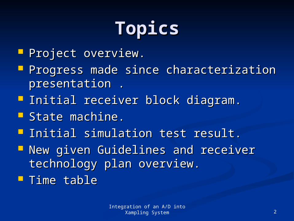
TopicsTopics Project overview.Project overview. Progress made since characterization Progress made since characterization
presentation .presentation . Initial receiver block diagram.Initial receiver block diagram. State machine.State machine. Initial simulation test result.Initial simulation test result. New given Guidelines and receiver New given Guidelines and receiver
technology plan overview.technology plan overview. Time tableTime table
Integration of an A/D into Xampling System

Project OverviewProject Overview
3Integration of an A/D into Xampling
System
Our goal is to integrate a sub-system that would Our goal is to integrate a sub-system that would convert the incoming analog samples to digital convert the incoming analog samples to digital signals. Then they will be processed and signals. Then they will be processed and reconstructed in the sub-Nyquist Sampling reconstructed in the sub-Nyquist Sampling system.system.
For this purpose we shall use the TI ADS6423 For this purpose we shall use the TI ADS6423 Evaluation module. Evaluation module.

Progress made since Progress made since characterization characterization
presentation presentation Understanding the system requirements.Understanding the system requirements. Acquisition of working tools (Quartus, ModelSim, Acquisition of working tools (Quartus, ModelSim,
ProcWizard).ProcWizard). Design of the initial receiver/transmitter.Design of the initial receiver/transmitter. Design of Control Logic for the circuit. Design of Control Logic for the circuit. Running Circuit Simulation on ModelSim for validation Running Circuit Simulation on ModelSim for validation
purposes.purposes. Analysis of Simulation Results. Analysis of Simulation Results. Research of ideal settings for Receiver Implementation. Research of ideal settings for Receiver Implementation.
4Integration of an A/D into Xampling
System

Initial transmitter-receiver block Initial transmitter-receiver block diagramdiagram
5Integration of an A/D into Xampling
System
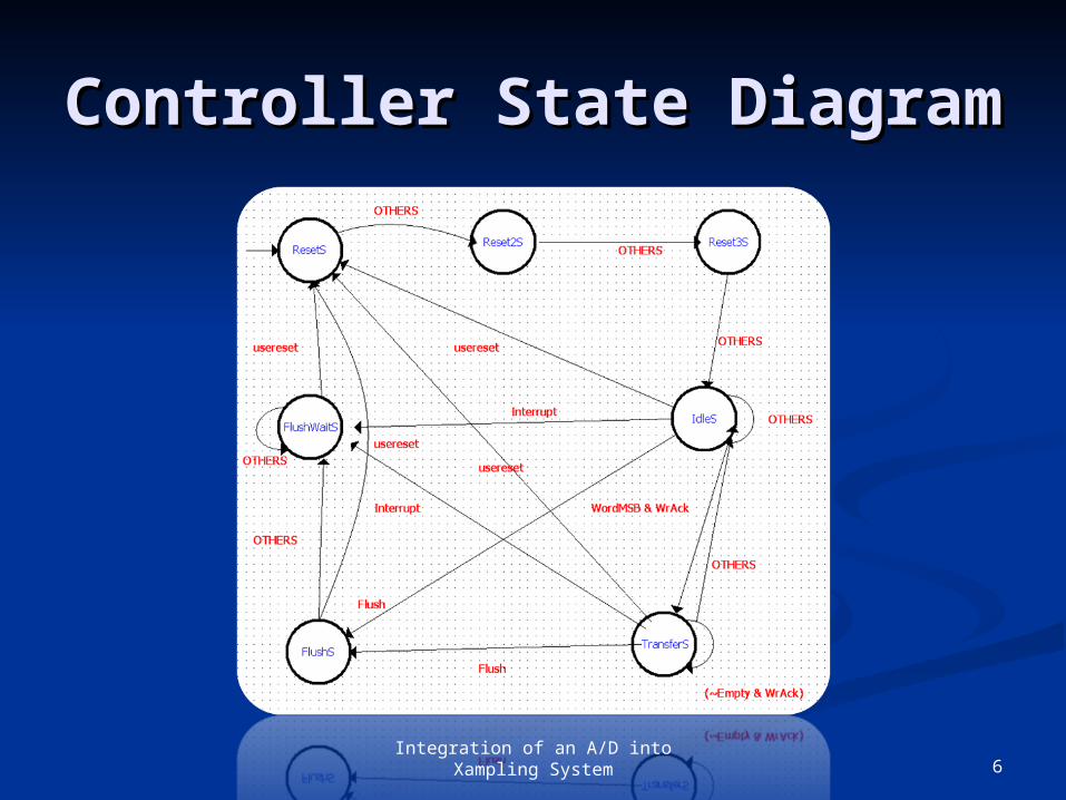
Controller State DiagramController State Diagram
6Integration of an A/D into Xampling
System

Controller State Machine Controller State Machine DiagramDiagram
7Integration of an A/D into Xampling
System

Initial simulation test Initial simulation test resultsresults
8Integration of an A/D into Xampling
System

The Altera Stratix III Differential The Altera Stratix III Differential signals Receiversignals Receiver
9Integration of an A/D into Xampling
System
The Stratix III device has dedicated The Stratix III device has dedicated circuitry to receive high-speed differential circuitry to receive high-speed differential signals. signals.
The receiver has a differential buffer, PLL, The receiver has a differential buffer, PLL, DPA block, synchronization FIFO buffer, DPA block, synchronization FIFO buffer, data realignment block, and a data realignment block, and a deserializer.deserializer.

New given Guidelines and our New given Guidelines and our plan for the receiver plan for the receiver
technology technology According to Gidel we shall not be able to According to Gidel we shall not be able to use Source Synchronous Receiver – almost use Source Synchronous Receiver – almost certain that it won’t work properly.certain that it won’t work properly.
We now aim to use a DPA (Dynamic Phase We now aim to use a DPA (Dynamic Phase Alignment) for the alignment of the data bits.Alignment) for the alignment of the data bits.
The BitSlip Mechanism will be used for word The BitSlip Mechanism will be used for word Synchronization.Synchronization.
The ADS6423 A/D card offers transmission The ADS6423 A/D card offers transmission test patterns that we intend to use. test patterns that we intend to use.
Single PSDB connection can mix LVDS and Single PSDB connection can mix LVDS and Non-LVDS pins.Non-LVDS pins.
10Integration of an A/D into Xampling
System

DPA CircuitryDPA Circuitry
11Integration of an A/D into Xampling
System

Bit Slip MechanismBit Slip Mechanism
12Integration of an A/D into Xampling
System
Skew in the transmitted data along with skew added by the link causeschannel-to-channel skew on the received serial data streams. If DPA is enabled, the received data is captured with different clock phases on each channel. This may cause the received data to be misaligned from channel to channel. To compensate for this channel-to-channel skew and establish the correct received word boundary at each channel, each receiver channel has a dedicated data realignment circuit that realigns the data by inserting bit latencies into the serial stream.

13
Time table (Semester A)Time table (Semester A)Task \ WeekTask \ Week 1111 1212 1313 1414
JulJuly1y1
JulJuly2y2
JulJuly3y3
July4
August1
August 2
August 3
ProcWizard Channel Lift
Design an adapter card
Design of the A/D Controller
Final Design of LVDS Receiver
Integration of the system
Form a debug strategy
30-01
Integration of an A/D into Xampling System

14
Questions / AnswersQuestions / Answers
Thank you!Thank you!
Integration of an A/D into Xampling System