![4 1 3 2 53'-8 2 [16356] 3 1 4 1234 1234 K A 4€¦ · 260'-3" [79336] 175'-8" [53548] 53'-10" [16418] 53'-8" [16356] 53'-8" [16350] 53'-8" [16356] 289'-9" [88314] 115'-8"[35248] 20'](https://static.fdocuments.in/doc/165x107/60d381bb815e453de71a57c7/4-1-3-2-53-8-2-16356-3-1-4-1234-1234-k-a-4-260-3-79336-175-8.jpg)
High-Speed-Board Design Techniques - Gonzaga...
28
Publication# 16356 Rev. B Amendment /0 Issue Date: February 1996 5-107 High-Speed-Board Design Techniques Application Note Advanced Micro Devices INTRODUCTION The most important factor in the design of many sys- tems today is speed. 66-MHz processors are common; 90- and 120-MHz processors are becoming readily available. The demand for high speed results from: a) the requirement that systems perform complex tasks in a time frame considered comfortable by humans; and b) the ability of component manufacturers to produce high- speed devices. An example of a) is the large amount of information that must be processed to perform even the most rudimentary computer animation. Currently, Pro- grammable Array Logic (PAL) devices are available with propagation delays of 4.5 ns, and complex PLDs such as MACH have propagation delays of 5 ns. While this might seem fast, it is not the propagation delay that cre- ates the potential for problems, but rather the fast edge rates needed to obtain the fast propagation delays. In the future, much faster devices will become available, with correspondingly faster edge rates. Designing high-speed systems requires not only fast components, but also intelligent and careful design. The analog aspect of the devices is as important as the digi- tal. In high-speed systems, noise generation is a prime concern. The high frequencies can radiate and cause in- terference. The corresponding fast edge rates can re- sult in ringing, reflections, and crosstalk. If unchecked, this noise can seriously degrade system performance. This application note presents an overview of the design of high-speed systems using a PC-board layout. It covers: ■ the power distribution system and its effect on board- noise generation, ■ transmission lines and their associated design rules, ■ crosstalk and its elimination, and ■ electromagnetic interference. 1. POWER DISTRIBUTION The most important consideration in high-speed board design is the power distribution network. For a noise- free board, it is necessary to have a noise-free power distribution network. Note that it is just as important to develop a clean VCC as it is to get a clean ground. For AC purposes, which is what this application note mainly dis- cusses, VCC is ground. The power distribution network also must provide a re- turn path for all signals generated or received on the board. This is often overlooked because the effect of the return path is less apparent at lower frequencies. Many designs work even when the nature of the return path is ignored. 1.1 Power Distribution Network as a Power Source 1.1.1 The Effect of Impedance Consider a 5” x 5” board with digital ICs and a power supply of +5.0 V. The goal is to deliver exactly +5.0 V to the power pins of every device on the board, regardless of its position relative to the power source. Furthermore, the voltage at the pins should be free of line noise. A power source with these characteristics would be schematically represented as an ideal voltage source (Figure 1a), which has zero impedance. Zero imped- ance would ensure that the load and source voltages would be the same. It also would mean that noise sig- nals would be absorbed because the noise generators have finite source impedance. Unfortunately, this is only an ideal. Figure 1b illustrates a real power source with associated impedances in the form of resistance, inductance, and capacitance. These are distributed over the power dis- tribution network. Because of the network’s impedance, noise signals can add to the voltage. The design goal is to reduce the power distribution net- work impedances as much as possible. There are two approaches: power buses and power planes. Power planes generally have better impedance characteristics than power buses; however, practical considerations might favor buses.
Transcript of High-Speed-Board Design Techniques - Gonzaga...
Publication# 16356 Rev. B Amendment /0
Issue Date: February 19965-107
High-Speed-Board Design Techniques
Application Note
AdvancedMicro
Devices
INTRODUCTIONThe most important factor in the design of many sys-tems today is speed. 66-MHz processors are common;90- and 120-MHz processors are becoming readilyavailable. The demand for high speed results from: a)the requirement that systems perform complex tasks ina time frame considered comfortable by humans; and b)the ability of component manufacturers to produce high-speed devices. An example of a) is the large amount ofinformation that must be processed to perform even themost rudimentary computer animation. Currently, Pro-grammable Array Logic (PAL) devices are available withpropagation delays of 4.5 ns, and complex PLDs suchas MACH have propagation delays of 5 ns. While thismight seem fast, it is not the propagation delay that cre-ates the potential for problems, but rather the fast edgerates needed to obtain the fast propagation delays. Inthe future, much faster devices will become available,with correspondingly faster edge rates.
Designing high-speed systems requires not only fastcomponents, but also intelligent and careful design. Theanalog aspect of the devices is as important as the digi-tal. In high-speed systems, noise generation is a primeconcern. The high frequencies can radiate and cause in-terference. The corresponding fast edge rates can re-sult in ringing, reflections, and crosstalk. If unchecked,this noise can seriously degrade system performance.
This application note presents an overview of the designof high-speed systems using a PC-board layout. Itcovers:
the power distribution system and its effect on board-noise generation,
transmission lines and their associated design rules,
crosstalk and its elimination, and
electromagnetic interference.
1. POWER DISTRIBUTIONThe most important consideration in high-speed boarddesign is the power distribution network. For a noise-
free board, it is necessary to have a noise-free powerdistribution network. Note that it is just as important todevelop a clean VCC as it is to get a clean ground. For ACpurposes, which is what this application note mainly dis-cusses, VCC is ground.
The power distribution network also must provide a re-turn path for all signals generated or received on theboard. This is often overlooked because the effect of thereturn path is less apparent at lower frequencies. Manydesigns work even when the nature of the return path isignored.
1.1 Power Distribution Network as a Power Source
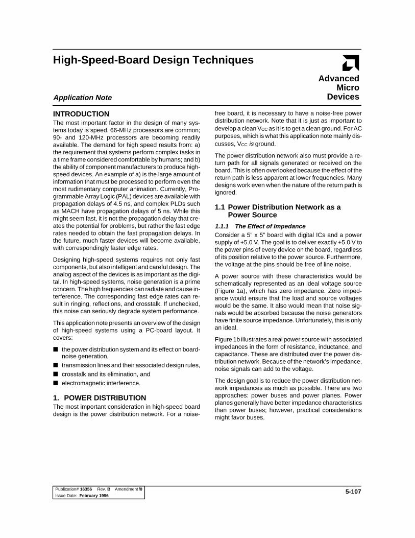
1.1.1 The Effect of ImpedanceConsider a 5” x 5” board with digital ICs and a powersupply of +5.0 V. The goal is to deliver exactly +5.0 V tothe power pins of every device on the board, regardlessof its position relative to the power source. Furthermore,the voltage at the pins should be free of line noise.
A power source with these characteristics would beschematically represented as an ideal voltage source(Figure 1a), which has zero impedance. Zero imped-ance would ensure that the load and source voltageswould be the same. It also would mean that noise sig-nals would be absorbed because the noise generatorshave finite source impedance. Unfortunately, this is onlyan ideal.
Figure 1b illustrates a real power source with associatedimpedances in the form of resistance, inductance, andcapacitance. These are distributed over the power dis-tribution network. Because of the network’s impedance,noise signals can add to the voltage.
The design goal is to reduce the power distribution net-work impedances as much as possible. There are twoapproaches: power buses and power planes. Powerplanes generally have better impedance characteristicsthan power buses; however, practical considerationsmight favor buses.
AMD
5-108 High-Speed-Board Design Techniques
LoadV +
V +VCC
t
VC
C (V
)
LoadV +
V +VCC
VC
C (V
)
t
16356A-001A
a)
b)
16356B-1
Figure 1. The Power Source. a) Ideal Representation; b) More Realistic Representation
U1 U2 U3
U4 U5 U6
U7 U8 U9
U1 U2 U3
U4 U5 U6
U7 U8 U9
16356A-002Aa) b) 16356B-2
Figure 2. Power Distributions System. a) Power Buses; b) Power Planes
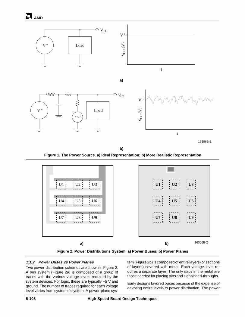
1.1.2 Power Buses vs Power PlanesTwo power-distribution schemes are shown in Figure 2.A bus system (Figure 2a) is composed of a group oftraces with the various voltage levels required by thesystem devices. For logic, these are typically +5 V andground. The number of traces required for each voltagelevel varies from system to system. A power-plane sys-
tem (Figure 2b) is composed of entire layers (or sectionsof layers) covered with metal. Each voltage level re-quires a separate layer. The only gaps in the metal arethose needed for placing pins and signal feed-throughs.
Early designs favored buses because of the expense ofdevoting entire levels to power distribution. The power

AMD
5-110 High-Speed-Board Design Techniques
a) b)
Capacitive In
duct
ive
ZC
(Ω)
FR (Freq.) FR (Freq.)
ZC
(Ω)
16356A-004A16356B-4
Figure 4. a) Capacitor Impedance Versus Frequency; b) the Effect of Lowering Capacitance While Using the Same Type of Construction (Constant ESL)
Metal Foil
Insulation
Metal Foil
16356A-005A16356B-5
Figure 5. Internal Construction of aLarge (> µF) Capacitor
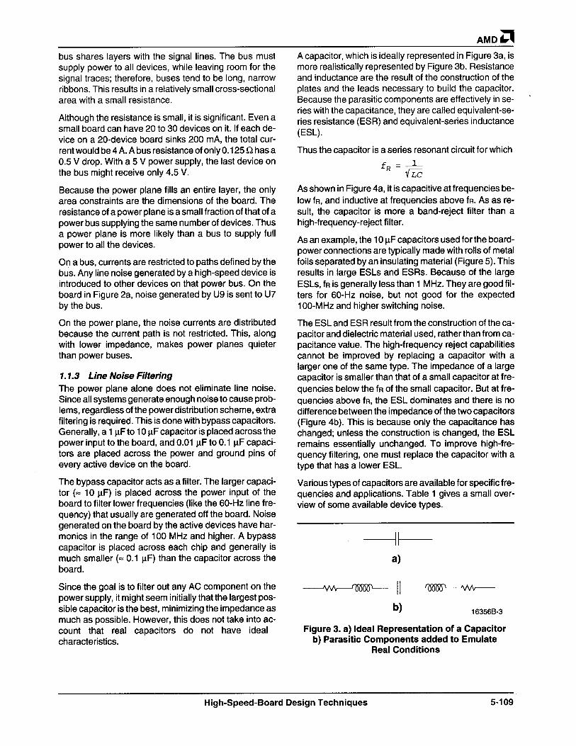
The lowest ESL capacitors often are made with non-fer-romagnetic materials, which have a low voltage-capaci-tance product. Thus it is difficult to make largecapacitors with practical breakdown voltages to preventboard failure. However, because of better filtering char-acteristics, larger values might not be needed. Figure 6compares a 0.01 µF capacitor of type C0G (non-ferro-magnetic) to a 0.1 µF capacitor of another type. Notethat the 0.01 µF capacitor gives better filtering at higherfrequencies.
The capacitor graphs imply that any one capacitor has alimited effective frequency operating range. Becausesystems have both high- and low-frequency noise, it isdesirable to extend this range. This can be done by put-ting a high-capacitance, low-ESL device in parallel witha lower-capacitance, very-low-ESL device. Figure 7shows that this can significantly increase the effectivefiltering frequency range.
1.1.4 Bypass Capacitor PlacementAfter the filter capacitors have been chosen, they mustbe placed on the board. Figure 8a shows the standardplacement for boards with slow device speeds. The ca-pacitor is placed near the top of the device to help en-sure its accessibility. While simple for layout, this doesnot give the best high-speed performance.
Note that the VCC capacitor connection is quite close tothe chip’s VCC connection, but the ground connection isfar away. Because noise is not uniform on a powerplane, the capacitor is not filtering noise at the chipleads; it is only filtering noise near the chip.
Table 1. Bypass Capacitor Groups
Type Range of Interest Application
Electrolytic 1 µF to > 20 µF Commonly used at power-supply connection on board.
Glass-Encapsulated Ceramic 0.01 µF to 0.1 µF Used as bypass capacitor at the chip. Also often placed in parallel with electrolytic to widen the filter bandwidth and increase the rejection band.
Ceramic-Chip 0.01 µF to 0.1 µF Primarily used at the chip. Also useful where low profile is important.
C0G < 0.1 µF Bypass for noise-sensitive devices. Often used in parallel with another ceramic chip to increase rejection band.

AMD
5-111High-Speed-Board Design Techniques
100.000
10.000
1.000
0.100
0.010
0.001
Z (
Ω)
0.1 1.0 10.0 100.0 1K
fR C0GfR X7R
0.01 µF C0G
0.1 µF X7R
Frequency (MHz)
16356A-006A16356B-6
Figure 6. Frequency Response of X7R and C0G Type Construction
XC
Frequency16356A-007A16356B-7
Figure 7. Frequency Response of Two Capacitors in Parallel
a) b) 16356A-008A16356B-8
Figure 8. a) Typical Placement of Bypass Capacitors; b) Preferred Placement of Bypass Capacitors
AMD
5-112 High-Speed-Board Design Techniques
Better performance can be obtained by ensuring thatthe chip and the capacitor contact the VCC and groundplanes at the same point. Because the capacitor size isdifferent from that of the chip, it is necessary to run twotraces from the VCC and ground plane contact points tothe capacitor, as shown in Figure 8b. These “lead exten-sions” are placed on a non-power plane and should bekept as short as possible. It is generally best to place thecapacitor on the opposite side of the board, directly un-der the chip. A surface-mount chip capacitor works wellhere.
Note that the “lead extension” traces from the capacitorto the power pins take up space that could have beenused for signal-line routing. However, putting extra ef-fort into routing the signal lines now could prevent muchnoise-reduction work later on.
For devices with multiple VCC and ground pins, how bestto bypass depends on the device. In particular, it de-pends on whether the power pins are connected inter-nally. On some devices, such as the PAL16R8-4 series,the ground pins are connected by a common groundbus. On these devices, it is only necessary to bypass
one ground pin to one VCC pin. If the power is kept sepa-rated internally, the separate VCC pins must bedecoupled individually. In general, it is best to contactthe device’s manufacturer for specific recommenda-tions.
1.2 Power Distribution Network as a Signal Return Path
One of the more surprising functions of the power net-work is the provision of a return path for all signals in thesystem, whether generated on or off the board. Designsthat accommodate this aspect of the power distributionsystem eliminate many high-speed noise problems.
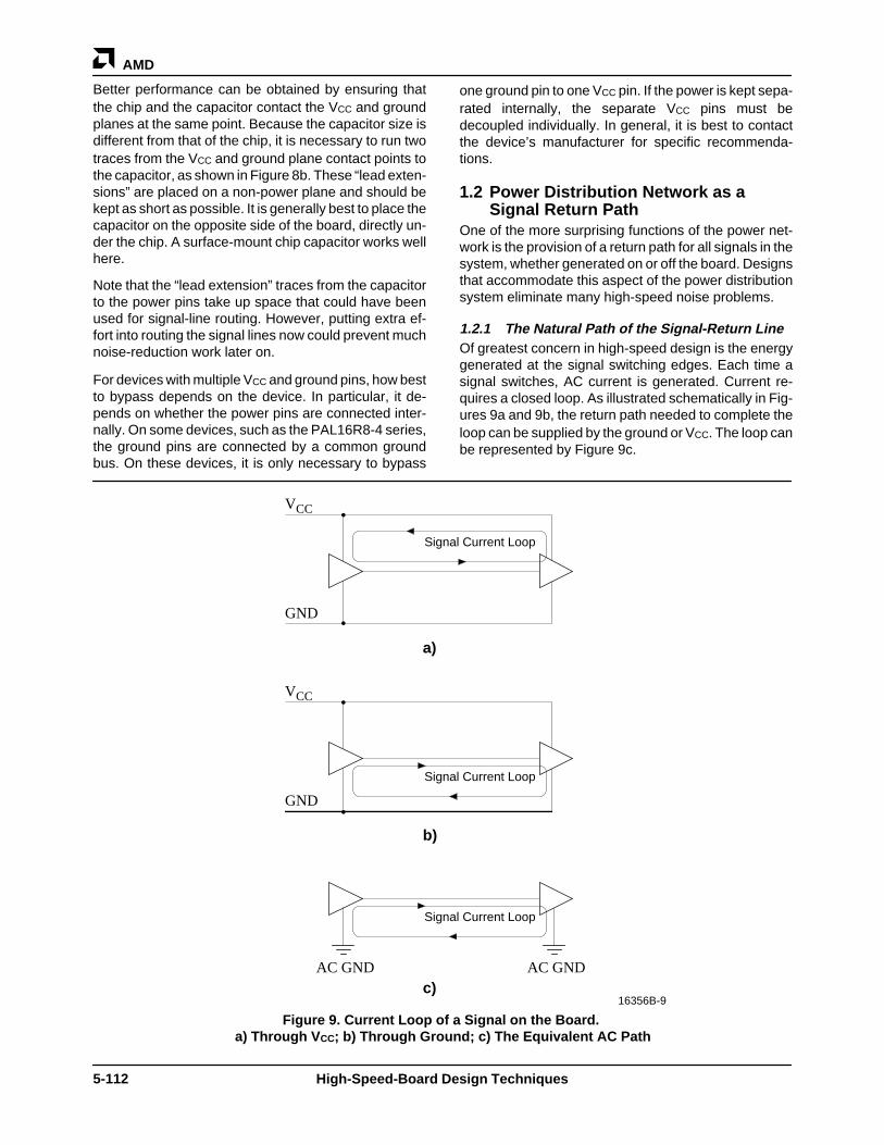
1.2.1 The Natural Path of the Signal-Return LineOf greatest concern in high-speed design is the energygenerated at the signal switching edges. Each time asignal switches, AC current is generated. Current re-quires a closed loop. As illustrated schematically in Fig-ures 9a and 9b, the return path needed to complete theloop can be supplied by the ground or VCC. The loop canbe represented by Figure 9c.
Signal Current Loop
a)
VCC
GND
Signal Current Loop
b)
VCC
GND
Signal Current Loop
c)AC GNDAC GND
16356A-009A16356B-9
Figure 9. Current Loop of a Signal on the Board. a) Through V CC; b) Through Ground; c) The Equivalent AC Path

AMD
5-113High-Speed-Board Design Techniques
d
l
i
i
L = Kl ln d - rr
r
16356A-010A16356B-10
Figure 10. Inductance Increases as the Signal andReturn Path are Separated
Current loops have inductance and can be thought of assingle-turn coils. They can aggravate ringing, crosstalk,and radiation. The current-loop inductance and associ-ated problems increase with loop size. Minimizing thesize of the loop minimizes these problems.
AC return signals have an entire plane in which tochoose a path, but they take the path of least impedance(not necessarily least resistance) to the current. Imped-ance also includes inductance and capacitance. Metalhas very little resistance; therefore, the impedance isprimarily inductive. Because impedance increases withinductance, the path of least impedance is the path withthe smallest inductance.
If the signal line goes from A to B on a random path, thenatural return path is not necessarily a straight line, aswould be dictated for least resistance. As noted in Fig-ure 10, the inductance of a signal line and its return lineincreases with the separation of the two paths. The path
of least impedance is the path bringing the signal-returnline closest to the signal line. If it can, the signal returnfollows the signal line as closely as possible, resulting inthe smallest loop. In multiple layer boards, “as closely aspossible” usually means in a ground or VCC plane aboveor below the signal trace. In a two-layer board, thismeans the closest ground or VCC trace.
1.2.2 Bus vs Planes for a Signal Return PathFigure 2a shows that a power bus has a fixed path. Thereturn signal must follow this path, whether optimal ornot. Unless the signal lines are purposely laid out nearthe power buses and oriented to minimize loop size,there will probably be large loops. If the layout of a boardusing buses for power distribution is not thought outcarefully, it can result in a configuration that generatesmuch noise.
The power plane imposes no natural restrictions on cur-rent flow. Thus the return signal can follow the path ofleast impedance, which is the path closest to the signalline. This results in the smallest possible current loops,which makes it the preferred solution for high-speedsystems.
Although power planes have an advantage over buses,the benefits they provide can be defeated by the de-signer. Any break in the natural path of the return signalforces it to go around the break, increasing the loop size(Figure 11). Be careful about cuts in the ground andpower planes.
1.3 Layout Rules With Power Distribution Considerations
The following layout rules will help you take advantageof power planes and avoid pitfalls.
Return Signal Plane
Break In Return Signal Plane
Current forced around break, increasing L
OutIn
16356A-011A16356B-11
Figure 11. The Increase in Loop Size Due to a Break in the Power Plane

AMD
5-114 High-Speed-Board Design Techniques
a. Be Careful with FeedthroughsCuts in the power plane tend to show up at feed-throughs or vias. These are necessary for traces tocross sides of the board and to connect componentsand connectors to the board. They are surrounded bysmall gaps where the power planes are etched away toavoid shorts in the signal lines. If the vias are close andthe etchings wide, they might touch and form a barrier toany return path. This can occur with backplane connec-tors and device sockets.
For example, this can occur on the connectors on VMEbackplanes. The 104-pin connector has vias that canblock the signal return. All the return signals are forcedto the edge of the board. Not only are the loops longer,but the edge is shared by all the return signals; as we willsee, this can result in crosstalk (Figure 12).
b. Ground Cables Sufficiently Current loop considerations are also applicable for ca-bles going off the board. Every signal should be a two-wire pair: one for the signal, and one for the return. The
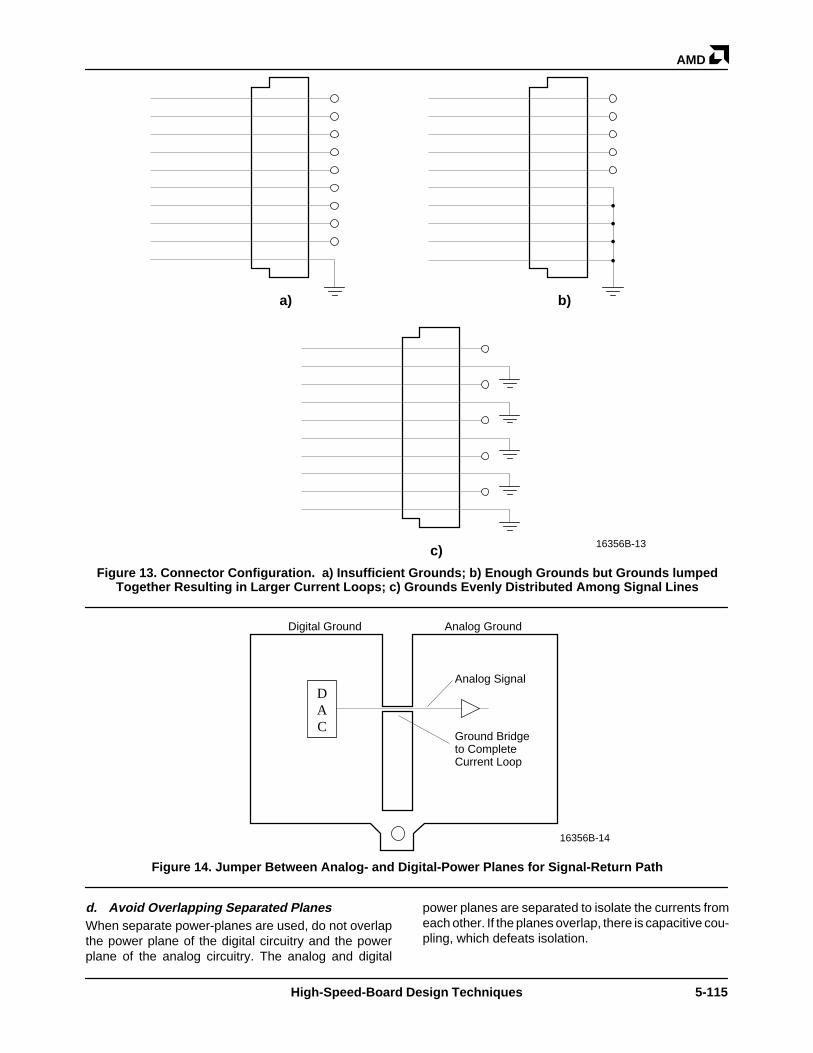
two lines should be kept next to each other to minimizethe loop size. Figures 13a and 13b illustrate poorer con-figurations. Figure 13c illustrates the proper configura-tion.
c. Separate Analog and Digital Power PlanesHigh-speed analog devices tend to be sensitive to digitalnoise. For example, amplifiers can amplify switchingnoise, making it appear as spikes. Thus on boards withanalog and digital functions, the power planes are com-monly separated; the planes are tied together at thepower source. This causes a problem for devices usingboth types of signals (such as DACs or voltage com-parators). The signal lines must cross the plane bounda-ries. These boundaries force the return path to thepower source before returning to the driver.
The solution is to place jumpers across the groundplanes where signals cross (Figure 14). The jumper pro-vides a bridge across the break for the return signal; thishelps minimize the current loop.
Common Return Path for A and B
Signal ‘A’
Return Path ‘A’
Signal ‘B’
Return Path ‘B’
16356A-012A16356B-12
Figure 12. Common Paths of Signal Return Due to Vias
AMD
5-115High-Speed-Board Design Techniques
a) b)
c) 16356A-013A16356B-13
Figure 13. Connector Configuration. a) Insufficient Grounds; b) Enough Grounds but Grounds lumpedTogether Resulting in Larger Current Loops; c) Grounds Evenly Distributed Among Signal Lines
D A C
Analog GroundDigital Ground
Analog Signal
Ground Bridge to Complete Current Loop
16356A-014A16356B-14
Figure 14. Jumper Between Analog- and Digital-Power Planes for Signal-Return Path
d. Avoid Overlapping Separated PlanesWhen separate power-planes are used, do not overlapthe power plane of the digital circuitry and the powerplane of the analog circuitry. The analog and digital
power planes are separated to isolate the currents fromeach other. If the planes overlap, there is capacitive cou-pling, which defeats isolation.

AMD
5-116 High-Speed-Board Design Techniques
To ensure separation, take a board and cut between theseparated planes. Then inspect the newly-exposededges of the board. No metal should be showing, exceptwhere traces or connections are specifically designed tocross the boundary.
e. Isolate Sensitive ComponentsCertain devices, such as phase-locked loops, are par-ticularly sensitive to noise interference. They require ahigher degree of isolation.
Good isolation can be achieved by etching a horseshoein the power planes around the device (Figure 15). Allsignals used by the device enter and leave through thenarrow gap at the end of the horseshoe. Noise currentson the power plane must go around the gap and do notcome close to the sensitive part.
When using this technique, ensure that all other signalsare routed away from the isolated section. The noisesignals generated by these lines can cause the interfer-ence this technique was designed to avoid.
f. Place Power Buses Near Signal LinesSometimes, the designer must use two-layer boardsand is forced to use power buses instead of planes.Even then it is possible to control loop size by placing thebuses as close as possible to the signal lines. Theground bus could follow the most sensitive signals onthe other side of the board (Figure 16). The loop for thatsignal is the same as it would be if the load used powerplanes.
2. Signal Lines as Transmission LinesControlling the relationship between the signal line andAC ground takes advantage of the return signal’s ten-dency to take the path of least impedance. Another ad-vantage is the constant impedance along the signal line.Such signal lines are called controlled-impedance lines,and they provide the best medium for signal transmis-sion on the board.
Noise- Sensitive Device
Gap in Power Planes
Corresponding Signal Lines
Ground Plane
Isolated Ground Plane
16356A-015A
Figure 15. Isolation of Noise Sensitive Components
16356B-15
Ground Line
Signal Line
16356A-016A
Figure 16. Providing the Optimum Signal-Return Path with a Bus-Power Distribution System
16356B-16


AMD
5-122 High-Speed-Board Design Techniques
VS VL0.66V
-0.04V
0.59V
0.26V
3.5V
-2.19V
2.24V
-1.21V
1.5
-2.84
2.21
-1.72
1.35
-2.84
2.21
-1.72
Time
16356A-023A16356B-23
Figure 23. Lattice Diagram Representation of a Reflected Signal
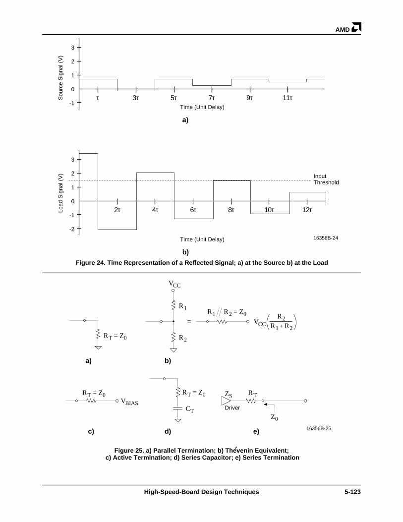
The same information in the time domain is shown inFigure 24. The top part of the Figure shows the source;the bottom shows the load signal. Note that it takes fivecomplete cycles for the signal strength to drop below theinput threshold. Propagation delays are typically from 2 ns/ft to 5 ns/ft. With tPD = 3 ns/ft and a 6-inch line, thedelay across the line is about 1.5 ns. The signal can besafely considered valid at about 13.5 ns after the originaltransition.
TERMINATIONThe amount of reflections shown in the last examplewould be too much for most systems. A technique isneeded to eliminated, or at least reduce, the reflections.Since the reflections are eliminated when ZL = Z0, it isnecessary to change ZL to equal Z0.
To understand this, look at the nature of the input andoutput impedances of the PAL devices. As noted above,input impedances tend to be high. Bipolar is in the 10 kΩrange, while CMOS is in the 100 kΩ range. Output driv-ers tend to have low impedance.
There are two schemes for termination: reduce ZL to Z0
to eliminate load reflections, or increase ZS to Z0 to elimi-nate secondary reflections at the source. ZL can be re-duced by placing a resistor in parallel with the load—parallel termination; ZS can be increased by placing aresistor in series with the source and the line—seriestermination.
Parallel termination is shown in Figure 25a. Because ofthe extremely high input resistance of most devices, RL
can be made equal to Z0.
AMD
5-123High-Speed-Board Design Techniques
Time (Unit Delay)
3
2
1
0
-1
a)
τ 3τ 5τ 7τ 9τ 11τSou
rce
Sig
nal (
V)
Time (Unit Delay)
3
2
1
0
-1
-2
b)
2τ 4τ 6τ 8τ 10τ 12τLoad
Sig
nal (
V) Input
Threshold
16356A-024A16356A-0A16356B-24
Figure 24. Time Representation of a Reflected Signal; a) at the Source b) at the Load
d)
RT = Z0VBIAS
RT = Z0
a)
c)
RT = Z0
CT
b)
R1
R2
=R1 R2 = Z0
VCC R2
R1 + R2
VCC
e)
RT
Driver
Z0
ZS
16356A-025A
Figure 25. a) Parallel Termination; b) Thevenin Equivalent; c) Active Termination; d) Series Capacitor; e) Series Termination
16356B-25


AMD
5-126 High-Speed-Board Design Techniques
1. Avoid DiscontinuitiesDiscontinuities are points where the impedance of thesignal line changes abruptly; they cause reflections. Theformula for KR is as valid here as it as at the end of theline. Because they cause reflections, they should beavoided. Discontinuities can be at sharp bends on thetrace or at vias through the board.
At bends on the trace, the cross-sectional area in-creases, and Z0 decreases. It is possible to compensatefor the bend by cutting the trace as shown in Figure 28.The cut is chosen so that the resulting diagonal is equalto the trace width. This minimizes the delta in cross-sec-
tional area, as well as the discontinuity. Using two 45°bends makes use of the same concept and is a commonway of smoothing out bends. A smooth circular arcwould be ideal but is harder to generate with many tools.
Vias take signals through the board to the other side(Figure 29). The vertical run of metal between layers isan uncontrolled impedance, and the more of these thereare, the greater is the overall amount of uncontrolled im-pedance in the line. This contributes to reflections. Also,the 90° bend from horizontal to vertical is a discontinuitythat generates reflections. If vias cannot be avoided,use as few as possible.
a)
w
b)
w
w
c)
w
w
w
d)
w
w
w
16356A-028A16356B-28
Figure 28. Reducing Discontinuity. a) Corner on PC Board Trace which Causes Discontinuity; Solved:b) by Shaving the Edge; c) by 45 ° Corner; d) by Using Curves

AMD
5-127High-Speed-Board Design Techniques
a)
y
Controlled Impedance
x
Uncontrolled Impedance
b)
y
x
Discontinuity
16356A-029A16356B-29
Figure 29. a) Excessive Number of Vias; b) Preferred Solution
Note that changing from an outer layer to an inside layer(or vice versa) generates an impedance change, sincethe design effectively is changed from stripline to micro-strip (or vice versa). While it is theoretically possible tochange geometries to compensate and keep imped-ances the same, it is very difficult to do so in production.The best results are obtained if outside signals remainoutside, and inside signals remain inside.
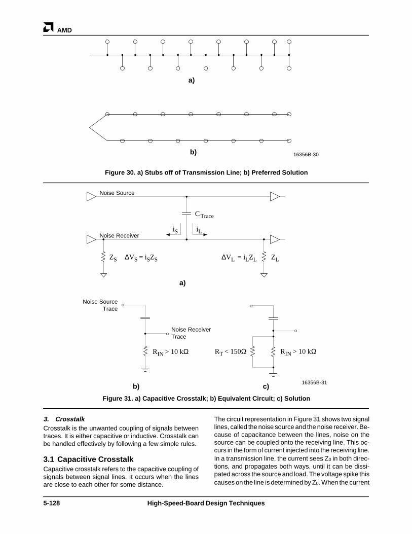
2. Do Not Use Stubs or TsWhen laying out the signal lines, it is often convenient torun stubs or Ts to the devices, similar to Figure 30a.Stubs and Ts can be noise sources. If long enough, they
are transmission lines with the main line as the sourceand are subject to the same type of reflections.
The signal lines should avoid long stubs and Ts. As longas the stubs are very short, a single line can be used witha single termination at the end, although Z0 must then bederated to account for the distributed load. Given the ex-ample in Figure 30a, if the stubs are too long, the signalline could be made into two signal lines, as shown in Fig-ure 30b. Both are transmission lines and require termi-nating; however, this is preferable to terminating eachlong stub individually.
AMD
5-128 High-Speed-Board Design Techniques
a)
b)16356A-030A
16356B-30
Figure 30. a) Stubs off of Transmission Line; b) Preferred Solution
iL
CTrace
ZS ZL
iS
Noise Source
Noise Receiver
∆VS = iSZS ∆VL = iLZL
Noise Source Trace
Noise Receiver Trace
RIN > 10 kΩ RIN > 10 kΩRT < 150Ω
a)
b) c) 16356A-031A16356B-31
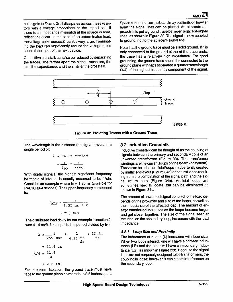
Figure 31. a) Capacitive Crosstalk; b) Equivalent Circuit; c) Solution
3. CrosstalkCrosstalk is the unwanted coupling of signals betweentraces. It is either capacitive or inductive. Crosstalk canbe handled effectively by following a few simple rules.
3.1 Capacitive CrosstalkCapacitive crosstalk refers to the capacitive coupling ofsignals between signal lines. It occurs when the linesare close to each other for some distance.
The circuit representation in Figure 31 shows two signallines, called the noise source and the noise receiver. Be-cause of capacitance between the lines, noise on thesource can be coupled onto the receiving line. This oc-curs in the form of current injected into the receiving line.In a transmission line, the current sees Z0 in both direc-tions, and propagates both ways, until it can be dissi-pated across the source and load. The voltage spike thiscauses on the line is determined by Z0. When the current

AMD
5-130 High-Speed-Board Design Techniques
a) b)
i1 i216356A-033A16356B-33
Figure 33. a) Inductive Crosstalk; b) Transformer Equivalent
a) c)b) 16356A-034A16356B-34
Figure 34. a) Artificial Loops; b) Schematic Equivalent; c) Solution
a) c)b)
i1
i2
i1
i2
16356A-035A16356B-35
Figure 35. a) Common Return Path; b) Loop; c) Autotransformer Equivalent Circuit
If portions of the return paths of two signal lines coincide,the resulting loops might form an auto-transformer (Fig-ure 35 a and c). An example of this is the VME-back-plane example discussed above. Ensuring that eachsignal has its own return path can eliminate this sourceof crosstalk.
3.2.2 Load ImpedanceIf inductive crosstalk comes about due to artificial loops,the solution is to open the loops. Unfortunately, locatingthe loops can often be a challenge. If the crosstalk isgenerated by natural signal / return-signal loops, then
clearly the loop cannot broken. But by keeping the loadimpedance low, the effect of the crosstalk can be mini-mized. Figure 36 shows a simplified schematic repre-sentation of a secondary “natural” loop with a load. HereZS is the intrinsic impedance of the secondary loop. Notethe series current (iS). Because the impedances are inseries, iS is the same everywhere in the loop. With a con-stant iS, the voltage drop is largest across the largest im-pedance. On an unterminated line, this usually is theload at the end of the line; i.e., at the input of the receiv-ing device.
AMD
5-131High-Speed-Board Design Techniques
Signal Line
Ground Return Path
ZS
RIN = 10 kΩ to 100 kΩ or greater
iS
16356A-036A16356B-36
Figure 36. Series Inductive Loop
Large noise signals are most unwanted at the inputs,where noise signals should be minimal. If the maximumsignal is developed across the largest impedance, thesignal developed at the input can be reduced by termi-nating the signal line at the receiver end, which reducesRIN to RT.
RT is usually in the 30 Ω to 150 Ω range. This reductionin RIN is at least two orders of magnitude. The voltagedrop across RIN is reduced accordingly. The exact dropis difficult to predict because it depends on the value ofZS , which is difficult to determine. But reducing RIN byorders of magnitude should have a significant effect.
3.3 Crosstalk Solutions SummaryThe following steps summarize the ways in which the ef-fects of crosstalk can be minimized.
1. The effect of both capacitive and inductive crosstalkincreases with load impedance. Thus all lines sus-ceptible to interference due to crosstalk should beterminated at the line impedance.
2. Keeping the signal lines separated reduces the en-ergy that can be capacitively coupled between signallines.
3. Capacitive coupling can be reduced by separatingthe signal lines by a ground line. To be effective, theground trace should be connected to the groundplane every λ/4 inches.
4. For inductive crosstalk, the loop size should be re-duced as much as possible. Where possible, loopsshould be eliminated.
5. For inductive crosstalk, avoid situations where signalreturn lines share a common path.
4. ELECTRO-MAGNETIC INTERFERENCE(EMI)
EMI is becoming more critical with speed. High-speeddevices are naturally more susceptible to interference.They accept fast glitches, which slower devices ignore.Even if the board or system is not susceptible, the FCCin the United States, along with VDE and CCITT inEurope, places severe limitations on the high-frequencynoise (both radiated and line noise) that the board cangenerate.
The designer can reduce EMI through shielding, filter-ing, eliminating current loops, and reducing devicespeed where possible. Although shielding is outside thescope of this article, all the other issues are discussedas follows.
4.1 LoopsCurrent loops are an unavoidable part of every design.They act as antennae. Minimizing the effects of loops onEMI means minimizing the number of loops and the an-tenna efficiency of the loops. Do not create artificialloops; and keep the natural loops as small as possible.
1. Avoid artificial loops by ensuring that each signal linehas only one path between any two points.
2. Use power planes whenever possible. Groundplanes automatically result in the smallest naturalcurrent loop. When using ground planes, ensure thatthe signal-return line path is not blocked.
If power buses are necessary, have the fast-signallines run either over or next to a power bus.
4.2 FilteringFiltering is standard for power lines. It can also be usedon signal lines, but is recommended only as a last resort,when the source of the signal noise cannot be eliminated.
Three options are available for filtering: bypass capaci-tors, EMI filters, and ferrite beads. Bypass capacitorsare discussed in section 1. EMI filters are commerciallyavailable filters; they are available over a wide fre-quency range. Ferrite beads are ferrite ceramics thatadd inductance to any wire within their proximity. Theyare used as high-frequency suppressors.
4.2.1 EMI FiltersEMI filters are commercially manufactured devices de-signed to attenuate high-frequency noise. They areused primarily to filter out noise in power lines. They actto isolate the power outside the system (referred to asthe line) from the power inside the system (referred to asthe load). Their effect is bi-directional: they filter outnoise going into, and coming out of, the device or board.
EMI filters consist of combinations of inductors and ca-pacitors. In general, the configuration to use depends onthe impedance of the nodes to be connected. A capaci-tor should be connected to a high-impedance node; aninductor should be connected to a low-impedance node.EMI filters are available in variations of the followingconfigurations: feedthrough capacitor, L-Circuit, PI-Cir-cuit, and T-Circuit.
The feedthrough capacitor’s only component is a ca-pacitor (Figure 37a). It is a good choice when the im-pedances connected to the filter are high. Note that itprovides no high-frequency current isolation be-tween nodes.
The L-Circuit has an inductor on one side of a capaci-tance (Figure 37b). It works best when the line andload have a large difference in impedance. The in-ductive element is connected to the lowest impedance.

AMD
5-132 High-Speed-Board Design Techniques
The PI-Circuit has an inductor surrounded by two ca-pacitors (Figure 37c). PI filters are best when the lineand load impedances are high and when high levelsof attenuation are needed.
The T-filter has inductors on either side of the capaci-tor in a T fashion (Figure 37d). It is a good choicewhen both line and load impedances are low.
LC filters are rated according to insertion loss, which isthe amount of signal lost due to the insertion of the filter.Insertion loss is usually stated in decibels. Filter manu-
facturers provide graphs of their filters over prescribedfrequency ranges.
4.2.2 Ferrite Noise SuppressorsFerrite noise suppressors are ferrite ceramics placed inproximity to the conducting material. They are availableas beads for single wires and clamps for cables. Whenusing beads, the wire is placed through a hole in thebead (Figure 38a). When using clamps, the ferrite mate-rial is clamped around the cable (Figure 38b). Clampsare popular with ribbon cable.
d)c)
b)a)
16356A-037A16356B-37
Figure 37. Line-Noise Filters. a) Capacitor; b) LC Filter; c) PI Filter; d) T Filter
Ferrite Bead
Ferrite Clamp
a)
b)16356A-038A16356B-38
Figure 38. a) Ferrite Bead; b) Ferrite Clamp