High Precision Time and Frequency Counter for … · High Precision Time and Frequency Counter for...
11
High Precision Time and Frequency Counter for Mobile Applications R. SZPLET, Z. JACHNA, K. ROZYC, J. KALISZ Department of Electronic Engineering Military University of Technology Gen. S. Kaliskiego 2, 00-908 Warsaw 49 POLAND {rszplet, zjachna, krozyc, jkalisz}@wel.wat.edu.pl http://ztc.wel.wat.edu.pl Abstract: - This paper presents the design, architecture, operation, and test results of a high precision time interval and frequency counter made as a small, portable instrument with USB interface. Thanks to the use of advanced time interpolators integrated in a CMOS chip, the precision (standard deviation) below 35 ps was obtained at measured time interval from 0 to 200 ms. The frequency can be measured up to 3.5 GHz. Due to the very short dead time of the counter the maximum measurement rate of 5 million measurements per second is achieved. The dedicated control software creates a user-friendly and versatile graphic interface in Windows environment. Reprogrammable CMOS technology used in the counter allows easy customizing of the instrument to match many specific applications. Key-Words: - time interval counter, time digitizer, time-to-digital converter, time interpolation, two-stage interpolation 1 Introduction The precision time interval counters (TIC) are usually designed and manufactured in form of desktop instruments [1] or computer boards [2, 3]. In modern measurement and test systems frequently a portable TIC is needed, which may conveniently be used with a notebook or netbook. We present such a solution. The design of precision TICs traditionally has been based on the Nutt interpolation method and time-to-digital conversion using analog charging a capacitor [4]. In the modern designs a prevalent solution is the use of the digital coding lines, integrated in the CMOS ASIC [5 - 7], CPLD [8] or FPGA [9 - 11] chips. Other methods, e.g. based on pulse-shrinking [12, 13] or counting of periods of a high frequency signal [14] are used rarely. A single-stage conversion utilizes the tapped delay line whose propagation time covers a single period of the reference clock and is easy for implementation [15, 16]. The delay of a single cell of the line determines the resolution of the digitizer. Therefore in TICs with a high resolution (< 50 ps) and relatively low clock frequency (< 100 MHz) the delay line would contain hundreds of delay cells. Such a long coding delay line reveals large linearity error of conversion and high sensitivity to the temperature and supply voltage variations. To shorten the line length a two-stage interpolation method is used [9, 17, 18]. In the following sections 2.1 and 2.2 we present the architecture of a portable TIC controlled by a notebook via a USB interface, and the used measurement methods. The TIC containing a programmed FPGA device which integrates time counter with a two-stage interpolation, FIFO memory, and the control circuitry is presented in section 2.3 followed by the control software description (section 2.4). In section 3 we describe the specialized operation modes of the counter, including a high-rate frequency sampling, measurement of Allan deviation (ADEV), and measurement of Time-Interval Error (TIE). The test results of TIC are described in section 4. 2 Design 2.1 Time interval counter Figure 1 shows the block diagram of the TIC. The main timing inputs for Time-Interval (TI) measurement are A (Start) and B (Stop). The fast comparators (FC) allow to select the required threshold level of the input pulses. The voltage levels are set by the corresponding Digital-to-Analog Converters (DAC) and can be adjusted manually on the virtual desktop or automatically by the software procedure. The inputs can also accept both Start and Stop pulses appearing consecutively in a common mode on a single input. The standardized pulses from the comparator outputs are fed to the interpolation WSEAS TRANSACTIONS on CIRCUITS and SYSTEMS R. Szplet, Z. Jachna, K. Rozyc, J. Kalisz ISSN: 1109-2734 399 Issue 6, Volume 9, June 2010
Transcript of High Precision Time and Frequency Counter for … · High Precision Time and Frequency Counter for...
High Precision Time and Frequency Counter for Mobile Applications
R. SZPLET, Z. JACHNA, K. ROZYC, J. KALISZ Department of Electronic Engineering
Military University of Technology Gen. S. Kaliskiego 2, 00-908 Warsaw 49
POLAND {rszplet, zjachna, krozyc, jkalisz}@wel.wat.edu.pl http://ztc.wel.wat.edu.pl
Abstract: - This paper presents the design, architecture, operation, and test results of a high precision time interval and frequency counter made as a small, portable instrument with USB interface. Thanks to the use of advanced time interpolators integrated in a CMOS chip, the precision (standard deviation) below 35 ps was obtained at measured time interval from 0 to 200 ms. The frequency can be measured up to 3.5 GHz. Due to the very short dead time of the counter the maximum measurement rate of 5 million measurements per second is achieved. The dedicated control software creates a user-friendly and versatile graphic interface in Windows environment. Reprogrammable CMOS technology used in the counter allows easy customizing of the instrument to match many specific applications. Key-Words: - time interval counter, time digitizer, time-to-digital converter, time interpolation, two-stage interpolation
1 Introduction The precision time interval counters (TIC) are usually designed and manufactured in form of desktop instruments [1] or computer boards [2, 3]. In modern measurement and test systems frequently a portable TIC is needed, which may conveniently be used with a notebook or netbook. We present such a solution.
The design of precision TICs traditionally has been based on the Nutt interpolation method and time-to-digital conversion using analog charging a capacitor [4]. In the modern designs a prevalent solution is the use of the digital coding lines, integrated in the CMOS ASIC [5 - 7], CPLD [8] or FPGA [9 - 11] chips. Other methods, e.g. based on pulse-shrinking [12, 13] or counting of periods of a high frequency signal [14] are used rarely. A single-stage conversion utilizes the tapped delay line whose propagation time covers a single period of the reference clock and is easy for implementation [15, 16]. The delay of a single cell of the line determines the resolution of the digitizer. Therefore in TICs with a high resolution (< 50 ps) and relatively low clock frequency (< 100 MHz) the delay line would contain hundreds of delay cells. Such a long coding delay line reveals large linearity error of conversion and high sensitivity to the temperature and supply voltage variations. To shorten the line length a two-stage interpolation method is used [9, 17, 18].
In the following sections 2.1 and 2.2 we present the architecture of a portable TIC controlled by a notebook via a USB interface, and the used measurement methods. The TIC containing a programmed FPGA device which integrates time counter with a two-stage interpolation, FIFO memory, and the control circuitry is presented in section 2.3 followed by the control software description (section 2.4). In section 3 we describe the specialized operation modes of the counter, including a high-rate frequency sampling, measurement of Allan deviation (ADEV), and measurement of Time-Interval Error (TIE). The test results of TIC are described in section 4.
2 Design 2.1 Time interval counter Figure 1 shows the block diagram of the TIC. The main timing inputs for Time-Interval (TI) measurement are A (Start) and B (Stop). The fast comparators (FC) allow to select the required threshold level of the input pulses. The voltage levels are set by the corresponding Digital-to-Analog Converters (DAC) and can be adjusted manually on the virtual desktop or automatically by the software procedure. The inputs can also accept both Start and Stop pulses appearing consecutively in a common mode on a single input. The standardized pulses from the comparator outputs are fed to the interpolation
WSEAS TRANSACTIONS on CIRCUITS and SYSTEMS R. Szplet, Z. Jachna, K. Rozyc, J. Kalisz
ISSN: 1109-2734 399 Issue 6, Volume 9, June 2010
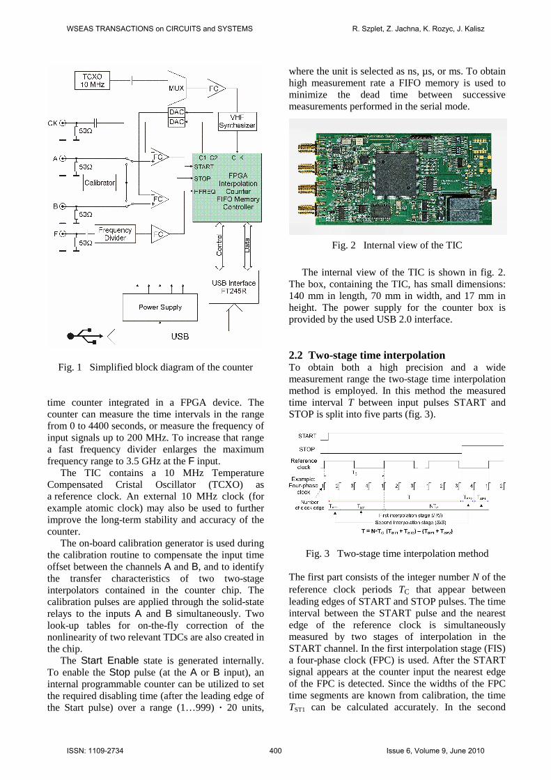
Fig. 1 Simplified block diagram of the counter time counter integrated in a FPGA device. The counter can measure the time intervals in the range from 0 to 4400 seconds, or measure the frequency of input signals up to 200 MHz. To increase that range a fast frequency divider enlarges the maximum frequency range to 3.5 GHz at the F input.
The TIC contains a 10 MHz Temperature Compensated Cristal Oscillator (TCXO) as a reference clock. An external 10 MHz clock (for example atomic clock) may also be used to further improve the long-term stability and accuracy of the counter.
The on-board calibration generator is used during the calibration routine to compensate the input time offset between the channels A and B, and to identify the transfer characteristics of two two-stage interpolators contained in the counter chip. The calibration pulses are applied through the solid-state relays to the inputs A and B simultaneously. Two look-up tables for on-the-fly correction of the nonlinearity of two relevant TDCs are also created in the chip.
The Start Enable state is generated internally. To enable the Stop pulse (at the A or B input), an internal programmable counter can be utilized to set the required disabling time (after the leading edge of the Start pulse) over a range (1…999) · 20 units,
where the unit is selected as ns, µs, or ms. To obtain high measurement rate a FIFO memory is used to minimize the dead time between successive measurements performed in the serial mode.
Fig. 2 Internal view of the TIC
The internal view of the TIC is shown in fig. 2. The box, containing the TIC, has small dimensions: 140 mm in length, 70 mm in width, and 17 mm in height. The power supply for the counter box is provided by the used USB 2.0 interface. 2.2 Two-stage time interpolation To obtain both a high precision and a wide measurement range the two-stage time interpolation method is employed. In this method the measured time interval T between input pulses START and STOP is split into five parts (fig. 3).
Fig. 3 Two-stage time interpolation method
The first part consists of the integer number N of the reference clock periods TC that appear between leading edges of START and STOP pulses. The time interval between the START pulse and the nearest edge of the reference clock is simultaneously measured by two stages of interpolation in the START channel. In the first interpolation stage (FIS) a four-phase clock (FPC) is used. After the START signal appears at the counter input the nearest edge of the FPC is detected. Since the widths of the FPC time segments are known from calibration, the time TST1 can be calculated accurately. In the second
WSEAS TRANSACTIONS on CIRCUITS and SYSTEMS R. Szplet, Z. Jachna, K. Rozyc, J. Kalisz
ISSN: 1109-2734 400 Issue 6, Volume 9, June 2010
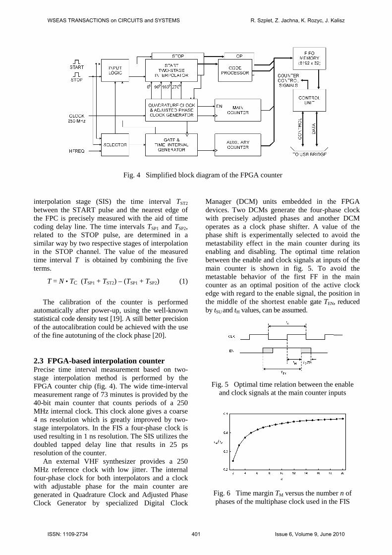
Fig. 4 Simplified block diagram of the FPGA counter
interpolation stage (SIS) the time interval TST2 between the START pulse and the nearest edge of the FPC is precisely measured with the aid of time coding delay line. The time intervals TSP1 and TSP2, related to the STOP pulse, are determined in a similar way by two respective stages of interpolation in the STOP channel. The value of the measured time interval T is obtained by combining the five terms.
T = N • TC (TSP1 + TST2) – (TSP1 + TSP2) (1)
The calibration of the counter is performed
automatically after power-up, using the well-known statistical code density test [19]. A still better precision of the autocalibration could be achieved with the use of the fine autotuning of the clock phase [20]. 2.3 FPGA-based interpolation counter Precise time interval measurement based on two-stage interpolation method is performed by the FPGA counter chip (fig. 4). The wide time-interval measurement range of 73 minutes is provided by the 40-bit main counter that counts periods of a 250 MHz internal clock. This clock alone gives a coarse 4 ns resolution which is greatly improved by two-stage interpolators. In the FIS a four-phase clock is used resulting in 1 ns resolution. The SIS utilizes the doubled tapped delay line that results in 25 ps resolution of the counter.
An external VHF synthesizer provides a 250 MHz reference clock with low jitter. The internal four-phase clock for both interpolators and a clock with adjustable phase for the main counter are generated in Quadrature Clock and Adjusted Phase Clock Generator by specialized Digital Clock
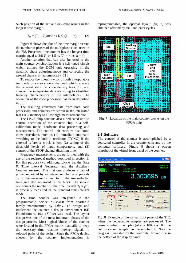
Manager (DCM) units embedded in the FPGA devices. Two DCMs generate the four-phase clock with precisely adjusted phases and another DCM operates as a clock phase shifter. A value of the phase shift is experimentally selected to avoid the metastability effect in the main counter during its enabling and disabling. The optimal time relation between the enable and clock signals at inputs of the main counter is shown in fig. 5. To avoid the metastable behavior of the first FF in the main counter as an optimal position of the active clock edge with regard to the enable signal, the position in the middle of the shortest enable gate TEN, reduced by tSU and tH values, can be assumed.
Fig. 5 Optimal time relation between the enable
and clock signals at the main counter inputs
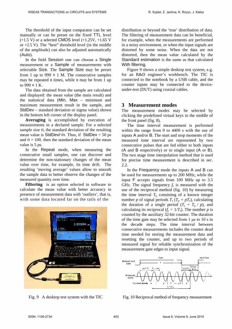
Fig. 6 Time margin TM versus the number n of phases of the multiphase clock used in the FIS
WSEAS TRANSACTIONS on CIRCUITS and SYSTEMS R. Szplet, Z. Jachna, K. Rozyc, J. Kalisz
ISSN: 1109-2734 401 Issue 6, Volume 9, June 2010
Such position of the active clock edge results in the longest time margin.
TM = (TC – TC/n)/2 = (TC/2)(1 – 1/n) (2)
Figure 6 shows the plot of the time margin versus
the number of phases of the multiphase clock used in the FIS. Presented time counter has the longest time margin equal to 3/8 TC or 1.5 ns (TC = 4 ns, n = 4).
Another solution that can also be used to the main counter synchronization is a self-tuned circuit which utilizes the DCM unit operating in the dynamic phase adjusting mode and correcting the needed phase shift automatically [21].
To reduce the linearity error of both interpolators two code processors were designed which execute the relevant statistical code density tests [19] and convert the interpolator data according to identified linearity characteristics of the interpolators. The operation of the code processors has been described in [9].
The resulting converted data from both code processors and counters are stored in the integrated fast FIFO memory to allow high measurement rate.
The FPGA chip contains also a dedicated unit to control operation of the counter chip in a self-calibration mode, hardware data processing and measurement. The control unit executes also some other procedures, such as (1) immediate automatic switching to the built-in oscillator (TCXO) if the external reference clock is lost, (2) setting of the threshold levels of input comparators, and (3) control of the STOP channel disabling time.
Frequency measurements are performed with the use of the reciprocal method described in section 3. For this purpose two additional blocks i.e. the Gate & Time Interval Generator and the Auxiliary Counter are used. The first one produces a pair of pulses separated by an integer number p of periods TS of the measured signal to fit the user-selected time gate also generated in this block. The second one counts the number p. The time interval TP = pTS is precisely measured in the standard time-interval mode.
The time counter was integrated in the programmable device XC3S400 from Spartan-3 family manufactured by Xilinx. To design and implement the counter a design environment ISE Foundation v. 10.1 (Xilinx) was used. The layout design was one of the most important phases of the design process. Most logical blocks of the counter were located in the FPGA matrix manually to keep the necessary time relations between signals in selected paths of the design. Since the FPGA device chosen for the counter implementation is
reprogrammable, the optimal layout (fig. 7) was obtained after many trial-and-error cycles.
Fig. 7 Location of the main counter blocks on the FPGA chip
2.4 Software The control of the counter is accomplished by a dedicated controller in the counter chip and by the computer software. Figure 8 shows a screen snapshot of the virtual front panel of the counter.
Fig. 8 Example of the virtual front panel of the TIC, when the consecutive samples are processed. The preset number of samples (of size 1000) is 100, the last processed sample has the number 38. Note the progress illustrated by the horizontal broken line in the bottom of the display panel.
WSEAS TRANSACTIONS on CIRCUITS and SYSTEMS R. Szplet, Z. Jachna, K. Rozyc, J. Kalisz
ISSN: 1109-2734 402 Issue 6, Volume 9, June 2010
The threshold of the input comparator can be set manually or can be preset on the fixed TTL level (+1.5 V) or a selected CMOS level (+1.25V, +1.65 V or +2.5 V). The “best” threshold level (in the middle of the amplitude) can also be adjusted automatically (Auto).
In the field Session one can choose a Single measurement or a Sample of measurements with selectable Size. The Sample Size may be preset from 1 up to 999 × 1 M. The consecutive samples may be repeated x times, while x may be from 1 up to 999 × 1 K.
The data obtained from the sample are calculated and displayed: the mean value (the main result) and the statistical data (Min, Max – minimum and maximum measurement result in the sample, and StdDev – standard deviation or sigma value) shown in the bottom left corner of the display panel.
Averaging is accomplished by execution of measurements in a declared sample. For a selected sample size n, the standard deviation of the resulting mean value is StdDev/√n. Thus, if StdDev = 50 ps and n = 100, then the standard deviation of the mean value is 5 ps.
In the Repeat mode, when measuring the consecutive small samples, one can discover and determine the non-stationary changes of the mean value over time, for example, its time drift. The resulting ‘moving average’ values allow to smooth the sample data to better observe the changes of the measured quantity over time.
Filtering is an option selected in software to calculate the mean value with better accuracy in presence of measurement data with ‘outliers’, that is, with some data located far on the tails of the
Fig. 9 A desktop test system with the TIC
distribution or beyond the ‘true’ distribution of data. The filtering of measurement data can be beneficial, for example, when the measurements are performed in a noisy environment, or when the input signals are distorted by some noise. When the data are not distorted, then the mean value calculated by the Standard estimation is the same as that calculated With filtering.
Figure 9 shows a simple desktop test system, e.g. for an R&D engineer’s workbench. The TIC is connected to the notebook by a USB cable, and the counter inputs may be connected to the device-under-test (DUT) using coaxial cables.
3 Measurement modes The measurement modes may be selected by clicking the predefined virtual keys in the middle of the front panel (fig. 8).
The time interval measurement is performed within the range from 0 to 4400 s with the use of inputs A and/or B. The start and stop moments of the measured time interval are represented by two consecutive pulses that are fed either to both inputs (A and B respectively) or to single input (A or B). The two stage time interpolation method that is used for precise time measurement is described in sec. 2.2.
In the Frequency mode the inputs A and B can be used for measurements up to 200 MHz, while the input F accepts signals from 100 MHz up to 3.5 GHz. The signal frequency fs is measured with the use of the reciprocal method (fig. 10) by measuring the time interval Tp consisting of a known integer number p of signal periods Ts (Tp = pTs), calculating the duration of a single period (Ts = Tp / p), and calculating its reciprocal (fs = 1/Ts). The number p is counted by the auxiliary 32-bit counter. The duration of the time gate may be selected from 1 µs to 10 s in the decade steps. The time interval between consecutive measurements includes the counter dead time needed for storing the measurement data and resetting the counter, and up to two periods of measured signal for reliable synchronization of the measurement gate edges to input signal.
Fig. 10 Reciprocal method of frequency measurement
WSEAS TRANSACTIONS on CIRCUITS and SYSTEMS R. Szplet, Z. Jachna, K. Rozyc, J. Kalisz
ISSN: 1109-2734 403 Issue 6, Volume 9, June 2010
3.1 Frequency sampling mode This mode allows for observation how the measured frequency varies in time. The principle of the frequency sampling using the reciprocal method is basically the same as presented in fig. 10. However, in this case the frequency of gate repetition is user-selected and strictly maintained. The gate duration is matched to the gate repetition period to obtain the maximum accuracy.
Thanks to the short dead time of the counter, the sampling can be performed with an internally generated rate (from 100 kSa/s to 2 MSa/s). It allows for discovering a frequency modulation (needed or not) of the measured signal, as shows fig. 11.
Fig. 11 Frequency modulation discovered in the SAMPLING mode
3.2 Measurement of Allan deviation (ADEV)
The Allan deviation of a periodic input signal may be calculated using a set of n samples, or
successively measured frequency kf averaged over the interval τ
( )1 2
1
1
1 1( ) ( ) ( )
2( 1)
n
k kyk
f ff n
σ τ τ τ−
+=
= −− ∑ (3)
where f is the nominal frequency of the tested signal [22].
During the sampling interval τ the time duration Tp of a train of the counted number p of periods T of the tested signal is measured. Thus, for a k’th sample
kf = pk / Tpk. For a given k two adjacent frequency
samples are needed to compute the result. Therefore the Allan deviation is also called the ‘two-sample’ deviation.
Fig. 12 Measurement of frequency samples to calculate the Allan deviation
Fig. 13 Virtual front panel of the TIC operating in the ALLAN DEVIATION mode
Figure 12 illustrates the method used for
measuring the Allan deviation. The upper dot line presents an example of a random walk behavior of the instantaneous frequency f of the tested signal. We can assume that the frequency f = 1/T, where the period T is represented by the width of a single dot on the figure. The lower dashed line is a train of consecutive samples of frequency averaged in intervals of duration τ.
Figure 13 shows a screen snapshot in the ALLAN DEVIATION mode. The Observation Interval is approximately equal to nτ. When n = 999999 and τ = 0.1 s, the resulting observation interval would last over 27 hours. To Repeat m (1...100) times the observation interval one may write in the number m (default 1), thus specifying the Measurement Session of approximate length mnτ.
In the Continuous operation mode the successive measurement sessions may be repeated infinitely unless they are stopped by pressing Stop.
σ τ( )y
WSEAS TRANSACTIONS on CIRCUITS and SYSTEMS R. Szplet, Z. Jachna, K. Rozyc, J. Kalisz
ISSN: 1109-2734 404 Issue 6, Volume 9, June 2010
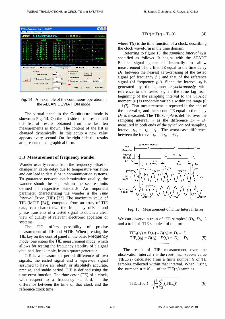
Fig. 14 An example of the continuous operation in the ALLAN DEVIATION mode
The virtual panel in the Continuous mode is
shown in Fig. 14. On the left side of the result field the list of results obtained from the last ten measurements is shown. The content of the list is changed dynamically. In this setup a new value appears every second. On the right side the results are presented in a graphical form. 3.3 Measurement of frequency wander
Wander usually results from the frequency offset or changes in cable delay due to temperature variation and can lead to data slips in communication systems. To guarantee network synchronization quality, the wander should be kept within the secure limits defined in respective standards. An important parameter characterizing the wander is the Time Interval Error (TIE) [23]. The maximum value of TIE (MTIE [24]), computed from an array of TIE data, can characterize the frequency offsets and phase transients of a tested signal to obtain a clear view of quality of relevant electronic apparatus or systems.
The TIC offers possibility of precise measurement of TIE and MTIE. When pressing the TIE key on the control panel in the basic Frequency mode, one enters the TIE measurement mode, which allows for testing the frequency stability of a signal obtained, for example, from a quartz generator.
TIE is a measure of period difference of two signals: the tested signal and a reference signal assumed to have an ‘ideal’, or absolutely accurate, precise, and stable period. TIE is defined using the time error function. The time error (TE) of a clock, with respect to a frequency standard, is the difference between the time of that clock and the reference clock time
TE(t) = T(t) – Tref(t) (4)
where T(t) is the time function of a clock, describing the clock waveform in the time domain.
Referring to figure 15, the sampling interval τ0 is specified as follows. It begins with the START Enable signal generated internally to allow measurement of the first TE equal to the time delay D1 between the nearest zero-crossing of the tested signal (of frequency ft ) and that of the reference signal (of frequency fr ). Since the interval τ0 is generated by the counter asynchronously with reference to the tested signal, the time lag from beginning of the sampling interval to the START moment (t1) is randomly variable within the range (0 – 1)Tt . That measurement is repeated in the end of the interval τ0 and the second TE equal to the delay D2 is measured. The TIE sample is defined over the sampling interval τ0 as the difference D2 – D1 measured in both ends of the synchronized sampling interval τ0s = t2 – t1. The worst-case difference between the interval τ0 and τ0s is ±Tt .
Fig. 15 Measurement of Time Interval Error We can observe a train of ‘TE samples’ (D1, D2,...) and a train of ‘TIE samples’ of the form
TIE1(τ0) = D(t2) – D(t1) = D2 – D1 TIE2(τ0) = D(t3) – D(t2) = D3 – D2 (5)
.............
The result of TIE measurement over the observation interval τ is the root-mean-square value TIErms(τ) calculated from a finite number N of TE samples collected within that interval. When using the number n = N – 1 of the TIE(τ0) samples
TIErms(τ0,τ) =2
1
1(TIE )
n
iin =∑ (6)
WSEAS TRANSACTIONS on CIRCUITS and SYSTEMS R. Szplet, Z. Jachna, K. Rozyc, J. Kalisz
ISSN: 1109-2734 405 Issue 6, Volume 9, June 2010
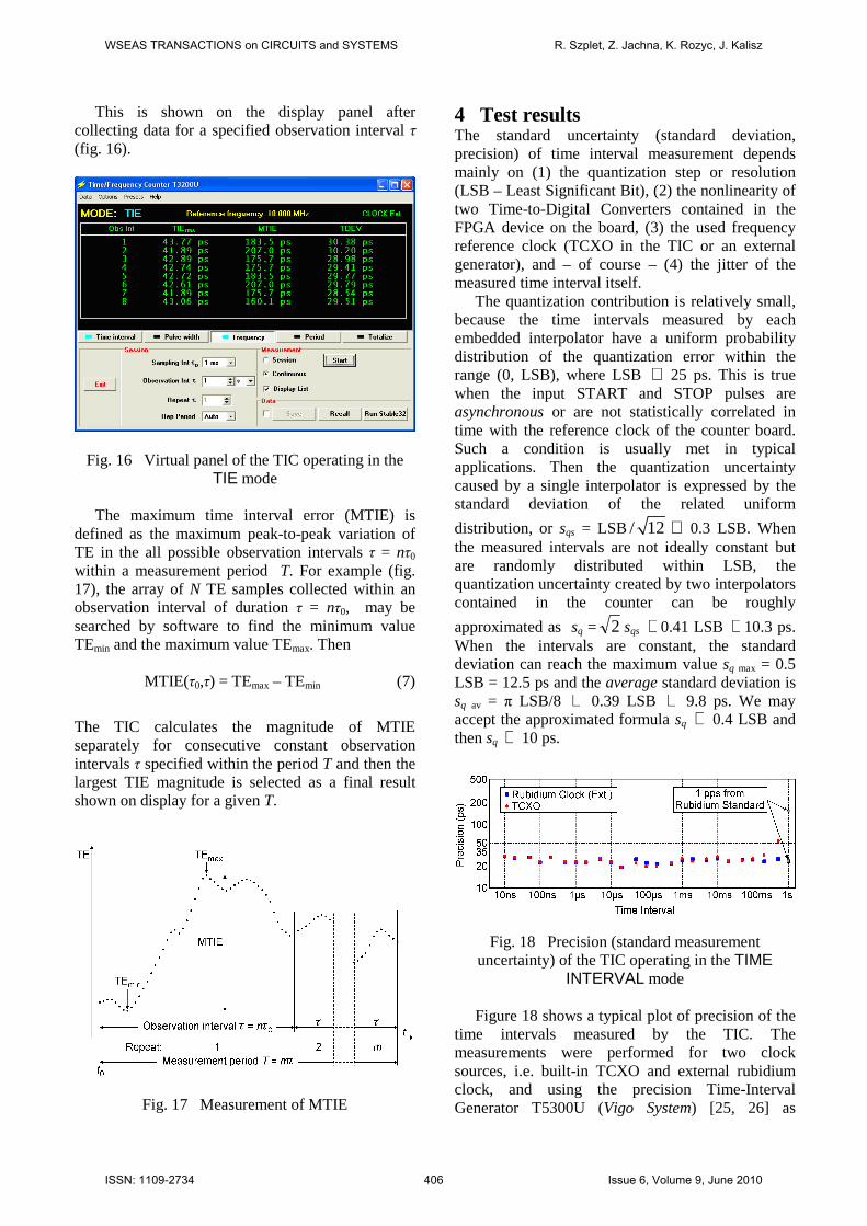
This is shown on the display panel after collecting data for a specified observation interval τ (fig. 16).
Fig. 16 Virtual panel of the TIC operating in the TIE mode
The maximum time interval error (MTIE) is
defined as the maximum peak-to-peak variation of TE in the all possible observation intervals τ = nτ0 within a measurement period T. For example (fig. 17), the array of N TE samples collected within an observation interval of duration τ = nτ0, may be searched by software to find the minimum value TEmin and the maximum value TEmax. Then
MTIE(τ0,τ) = TEmax – TEmin (7)
The TIC calculates the magnitude of MTIE separately for consecutive constant observation intervals τ specified within the period T and then the largest TIE magnitude is selected as a final result shown on display for a given T.
Fig. 17 Measurement of MTIE
4 Test results The standard uncertainty (standard deviation, precision) of time interval measurement depends mainly on (1) the quantization step or resolution (LSB – Least Significant Bit), (2) the nonlinearity of two Time-to-Digital Converters contained in the FPGA device on the board, (3) the used frequency reference clock (TCXO in the TIC or an external generator), and – of course – (4) the jitter of the measured time interval itself.
The quantization contribution is relatively small, because the time intervals measured by each embedded interpolator have a uniform probability distribution of the quantization error within the range (0, LSB), where LSB ≅ 25 ps. This is true when the input START and STOP pulses are asynchronous or are not statistically correlated in time with the reference clock of the counter board. Such a condition is usually met in typical applications. Then the quantization uncertainty caused by a single interpolator is expressed by the standard deviation of the related uniform
distribution, or sqs = LSB/ 12 ≅ 0.3 LSB. When the measured intervals are not ideally constant but are randomly distributed within LSB, the quantization uncertainty created by two interpolators contained in the counter can be roughly
approximated as sq = 2 sqs ≅ 0.41 LSB ≅ 10.3 ps. When the intervals are constant, the standard deviation can reach the maximum value sq max = 0.5 LSB = 12.5 ps and the average standard deviation is sq av = π LSB/8 ≅ 0.39 LSB ≅ 9.8 ps. We may accept the approximated formula sq ≅ 0.4 LSB and then sq ≅ 10 ps.
Fig. 18 Precision (standard measurement
uncertainty) of the TIC operating in the TIME INTERVAL mode
Figure 18 shows a typical plot of precision of the
time intervals measured by the TIC. The measurements were performed for two clock sources, i.e. built-in TCXO and external rubidium clock, and using the precision Time-Interval Generator T5300U (Vigo System) [25, 26] as
WSEAS TRANSACTIONS on CIRCUITS and SYSTEMS R. Szplet, Z. Jachna, K. Rozyc, J. Kalisz
ISSN: 1109-2734 406 Issue 6, Volume 9, June 2010
a source of the reference time intervals. This generator also adds its jitter to the observed result, but that contribution appeared smallest compared to other tested commercial delay generators. The value of that jitter does not exceed 15 ps within the tested time intervals. The two gray points in the figure show the data obtained when the 1-second intervals were produced by the pulses generated at the 1-PPS output of a Rubidium clock generator, and measured by the TIC every second pulse in the ‘Common Mode’ (Input A).
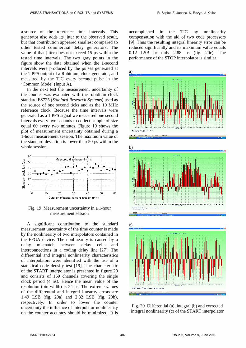
In the next test the measurement uncertainty of the counter was evaluated with the rubidium clock standard FS725 (Stanford Research Systems) used as the source of one second ticks and as the 10 MHz reference clock. Because the time intervals were generated as a 1 PPS signal we measured one second intervals every two seconds to collect sample of size equal 60 every two minutes. Figure 19 shows the plot of measurement uncertainty obtained during a 1-hour measurement session. The maximum value of the standard deviation is lower than 50 ps within the whole session.
Fig. 19 Measurement uncertainty in a 1-hour measurement session
A significant contribution to the standard
measurement uncertainty of the time counter is made by the nonlinearity of two interpolators contained in the FPGA device. The nonlinearity is caused by a delay mismatch between delay cells and interconnections in a coding delay line [27]. The differential and integral nonlinearity characteristics of interpolators were identified with the use of a statistical code density test [19]. The characteristic of the START interpolator is presented in figure 20 and consists of 169 channels covering the single clock period (4 ns). Hence the mean value of the resolution (bin width) is 24 ps. The extreme values of the differential and integral linearity errors are 1.49 LSB (fig. 20a) and 2.32 LSB (fig. 20b), respectively. In order to lower the counter uncertainty the influence of interpolator nonlinearity on the counter accuracy should be minimized. It is
accomplished in the TIC by nonlinearity compensation with the aid of two code processors [9]. Thus the resulting integral linearity error can be reduced significantly and its maximum value equals 0.12 LSB or only 2.88 ps (fig. 20c). The performance of the STOP interpolator is similar.
a)
b)
c)
Fig. 20 Differential (a), integral (b) and corrected integral nonlinearity (c) of the START interpolator
WSEAS TRANSACTIONS on CIRCUITS and SYSTEMS R. Szplet, Z. Jachna, K. Rozyc, J. Kalisz
ISSN: 1109-2734 407 Issue 6, Volume 9, June 2010
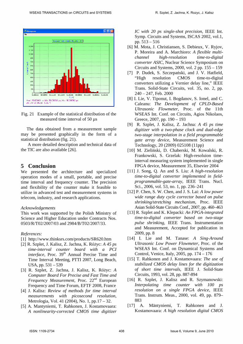
Fig. 21 Example of the statistical distribution of the measured time interval of 50 µs
The data obtained from a measurement sample
may be presented graphically in the form of a statistical distribution (fig. 21).
A more detailed description and technical data of the TIC are also available [26].
5 Conclusion We presented the architecture and specialized operation modes of a small, portable, and precise time interval and frequency counter. The precision and flexibility of the counter make it feasible to utilize in advanced test and measurement systems in telecom, industry, and research applications. Acknowledgements This work was supported by the Polish Ministry of Science and Higher Education under Contracts Nos. 0503/R/T02/2007/03 and 2984/B/T02/2007/33. References: [1] http://www.thinksrs.com/products/SR620.htm [2] R. Szplet, J. Kalisz, Z. Jachna, K. Różyc: A 45 ps
time-interval counter board with a PCI interface, Proc. 39th Annual Precise Time and Time Interval Meeting, PTTI 2007, Long Beach, USA, pp. 531 – 539
[3] R. Szplet, Z. Jachna, J. Kalisz, K. Różyc: A Computer Board For Precise and Fast Time and Frequency Measurement, Proc. 22nd European Frequency and Time Forum, EFTF 2008, France
[4] J. Kalisz: Review of methods for time interval measurements with picosecond resolution, Metrologia, Vol. 41 (2004), No. 1, pp.17 – 32.
[5] A. Mantyniemi, T. Rahkonen, J. Kostamovaara: A nonlinearity-corrected CMOS time digitizer
IC with 20 ps single-shot precision, IEEE Int. Symp. Circuits and Systems, ISCAS 2002, vol.1, pp. 513 – 516
[6] M. Mota, J. Christiansen, S. Debieux, V. Ryjov, P. Moreira and A. Marchioro: A flexible multi-channel high-resolution time-to-digital converter ASIC, Nuclear Science Symposium on Circuits and Systems, 2000, vol. 2 pp. 155 – 159
[7] P. Dudek, S. Szczepański, and J. V. Hatfield, “High resolution CMOS time-to-digital converters utilizing a Vernier delay line,” IEEE Trans. Solid-State Circuits, vol. 35, no. 2, pp. 240 – 247, Feb. 2000
[8] I. Lie, V. Tiponut, I. Bogdanov, S. Ionel, and C. Caleanu: The Development of CPLD-Based Ultrasonic Flowmeter, Proc. of the 11th WSEAS Int. Conf. on Circuits, Agios Nikolaos, Greece, 2007, pp. 190 – 193
[9] R. Szplet, J. Kalisz, Z. Jachna: A 45 ps time digitizer with a two-phase clock and dual-edge two-stage interpolation in a field programmable gate array device, Measurement Science and Technology, 20 (2009) 025108 (11pp)
[10] M. Zieliński, D. Chaberski, M. Kowalski, R. Frankowski, S. Grzelak: High-resoluion time-interval measuring system implemented in single FPGA device, Measurement 35, Elsevier 2004
[11] J. Song, Q. An and S. Liu: A high-resolution time-to-digital converter implemented in field-programmable-gate-array, IEEE Trans. Nucl. Sci., 2006, vol. 53, no. 1, pp. 236–241
[12] P. Chen, S. W. Chen, and J. S. Lai: A low power wide range duty cycle corrector based on pulse shrinking/stretching mechanism, Proc. IEEE Asian Solid-State Circuits Conf., 2007, pp. 460–463
[13] R. Szplet and K. Klepacki: An FPGA-integrated time-to-digital converter based on two-stage pulse shrinking, IEEE Trans. Instrumentation and Measurement, Accepted for publication in 2009, pp. 8
[14] I. Lie and M. Tanase: A Sing-Around Ultrasonic Low Power Flowmeter, Proc. of the WSEAS Int. Conf. on Dynamical Systems and Control, Venice, Italy, 2005, pp. 174 – 176
[15] T. Rahkonen and J. Kostamovaara: The use of stabilized CMOS delay lines for the digitization of short time intervals, IEEE J. Solid-State Circuits, 1993, vol. 28, pp. 887-894
[16] R. Szplet, J. Kalisz and R. Szymanowski: Interpolating time counter with 100 ps resolution on a single FPGA device, IEEE Trans. Instrum. Meas., 2000, vol. 49, pp. 879–883
[17] A. Mäntyniemi, T. Rahkonen and J. Kostamovaara: A high resolution digital CMOS
WSEAS TRANSACTIONS on CIRCUITS and SYSTEMS R. Szplet, Z. Jachna, K. Rozyc, J. Kalisz
ISSN: 1109-2734 408 Issue 6, Volume 9, June 2010
time-to-digital converter based on nested delay locked loops, Proc. IEEE Int. Symp. Circuits and Systems ISCAS’99, vol. 2, 1999
[18] R. Szymanowski and J. Kalisz Field programmable gate array time counter with two-stage interpolation, Rev. Sci. Instrum., 2005, 76 045104-1
[19] J. Kalisz, M. Pawłowski, and R. Pełka: Error analysis and design of the Nutt time-interval digitiser with picosecond resolution, J. Phys. E, Sci. Instrum., 1987, vol. 20, no. 11, pp. 1330–1341
[20] J. Kalisz, M. Pawłowski, and R. Pełka: A method for autocalibration of the interpolation time-interval digitiser with picosecond resolution, J. Phys. E, Sci. Instrum., 1985, vol.18, pp. 444- 452
[21] R. Szplet: Auto-tuned counter synchronization in FPGA-based interpolation time digitizers, Electronics Letters, 2009, vol. 45, no. 13
[22] http://tf.nist.gov/timefreq/general/pdf/868.pdf [23] ITU-T Recommendation G.810, Definitions and terminology for synchronization networks, 1996 [24] S. Bregni: Fast algorithms for TVAR and MTIE
computation in characterization of network synchronization performance, Advances in Signal Processing and Computer Technologies, WSEAS Press, 2001
[25] J. Kalisz, A. Poniecki, K. Różyc: A simple, precise, and low jitter delay/gate generator, Review of Scientific Instruments, Vol. 74 (2003), No. 7, pp. 3507-3509
[26] http://vigo.com.pl [27] B. Zhou, A. Mohammad and A. Khouas:
Investigation of single cell delay and delay mismatch in ring oscillator based test structure, Proc. of the 10th WSEAS Int. Conf. on Circuits, Athens, Greece, 2006, pp. 185-190
WSEAS TRANSACTIONS on CIRCUITS and SYSTEMS R. Szplet, Z. Jachna, K. Rozyc, J. Kalisz
ISSN: 1109-2734 409 Issue 6, Volume 9, June 2010