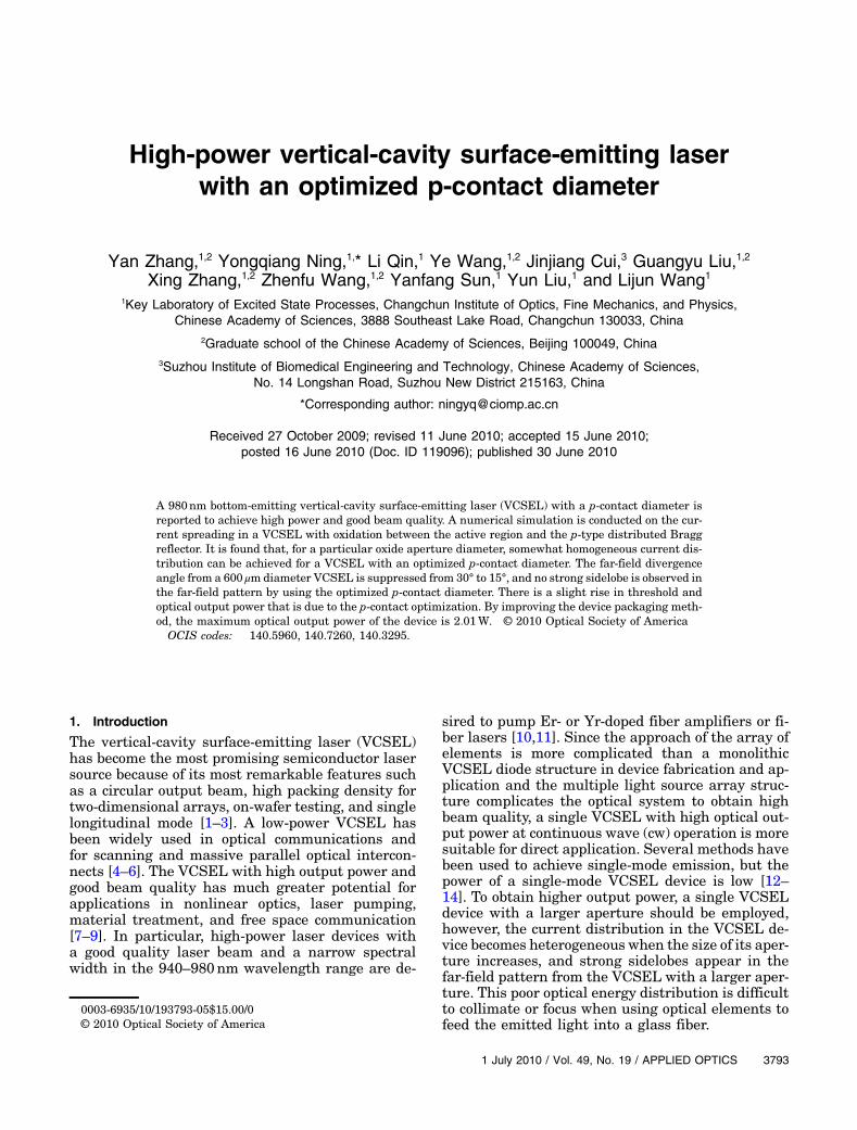
High-power vertical-cavity surface-emitting laser with an optimized p-contact diameter
5
High-power vertical-cavity surface-emitting laser with an optimized p-contact diameter Yan Zhang, 1,2 Yongqiang Ning, 1, * Li Qin, 1 Ye Wang, 1,2 Jinjiang Cui, 3 Guangyu Liu, 1,2 Xing Zhang, 1,2 Zhenfu Wang, 1,2 Yanfang Sun, 1 Yun Liu, 1 and Lijun Wang 1 1 Key Laboratory of Excited State Processes, Changchun Institute of Optics, Fine Mechanics, and Physics, Chinese Academy of Sciences, 3888 Southeast Lake Road, Changchun 130033, China 2 Graduate school of the Chinese Academy of Sciences, Beijing 100049, China 3 Suzhou Institute of Biomedical Engineering and Technology, Chinese Academy of Sciences, No. 14 Longshan Road, Suzhou New District 215163, China *Corresponding author: [email protected] Received 27 October 2009; revised 11 June 2010; accepted 15 June 2010; posted 16 June 2010 (Doc. ID 119096); published 30 June 2010 A 980 nm bottom-emitting vertical-cavity surface-emitting laser (VCSEL) with a p-contact diameter is reported to achieve high power and good beam quality. A numerical simulation is conducted on the cur- rent spreading in a VCSEL with oxidation between the active region and the p-type distributed Bragg reflector. It is found that, for a particular oxide aperture diameter, somewhat homogeneous current dis- tribution can be achieved for a VCSEL with an optimized p-contact diameter. The far-field divergence angle from a 600 μm diameter VCSEL is suppressed from 30° to 15°, and no strong sidelobe is observed in the far-field pattern by using the optimized p-contact diameter. There is a slight rise in threshold and optical output power that is due to the p-contact optimization. By improving the device packaging meth- od, the maximum optical output power of the device is 2:01 W. © 2010 Optical Society of America OCIS codes: 140.5960, 140.7260, 140.3295. 1. Introduction The vertical-cavity surface-emitting laser (VCSEL) has become the most promising semiconductor laser source because of its most remarkable features such as a circular output beam, high packing density for two-dimensional arrays, on-wafer testing, and single longitudinal mode [1–3]. A low-power VCSEL has been widely used in optical communications and for scanning and massive parallel optical intercon- nects [4–6]. The VCSEL with high output power and good beam quality has much greater potential for applications in nonlinear optics, laser pumping, material treatment, and free space communication [7–9]. In particular, high-power laser devices with a good quality laser beam and a narrow spectral width in the 940–980 nm wavelength range are de- sired to pump Er- or Yr-doped fiber amplifiers or fi- ber lasers [10,11]. Since the approach of the array of elements is more complicated than a monolithic VCSEL diode structure in device fabrication and ap- plication and the multiple light source array struc- ture complicates the optical system to obtain high beam quality, a single VCSEL with high optical out- put power at continuous wave (cw) operation is more suitable for direct application. Several methods have been used to achieve single-mode emission, but the power of a single-mode VCSEL device is low [12– 14]. To obtain higher output power, a single VCSEL device with a larger aperture should be employed, however, the current distribution in the VCSEL de- vice becomes heterogeneous when the size of its aper- ture increases, and strong sidelobes appear in the far-field pattern from the VCSEL with a larger aper- ture. This poor optical energy distribution is difficult to collimate or focus when using optical elements to feed the emitted light into a glass fiber. 0003-6935/10/193793-05$15.00/0 © 2010 Optical Society of America 1 July 2010 / Vol. 49, No. 19 / APPLIED OPTICS 3793
Transcript of High-power vertical-cavity surface-emitting laser with an optimized p-contact diameter
High-power vertical-cavity surface-emitting laserwith an optimized p-contact diameter
Yan Zhang,1,2 Yongqiang Ning,1,* Li Qin,1 Ye Wang,1,2 Jinjiang Cui,3 Guangyu Liu,1,2
Xing Zhang,1,2 Zhenfu Wang,1,2 Yanfang Sun,1 Yun Liu,1 and Lijun Wang1
1Key Laboratory of Excited State Processes, Changchun Institute of Optics, Fine Mechanics, and Physics,Chinese Academy of Sciences, 3888 Southeast Lake Road, Changchun 130033, China
2Graduate school of the Chinese Academy of Sciences, Beijing 100049, China3Suzhou Institute of Biomedical Engineering and Technology, Chinese Academy of Sciences,
No. 14 Longshan Road, Suzhou New District 215163, China
*Corresponding author: [email protected]
Received 27 October 2009; revised 11 June 2010; accepted 15 June 2010;posted 16 June 2010 (Doc. ID 119096); published 30 June 2010
A 980nm bottom-emitting vertical-cavity surface-emitting laser (VCSEL) with a p-contact diameter isreported to achieve high power and good beam quality. A numerical simulation is conducted on the cur-rent spreading in a VCSEL with oxidation between the active region and the p-type distributed Braggreflector. It is found that, for a particular oxide aperture diameter, somewhat homogeneous current dis-tribution can be achieved for a VCSEL with an optimized p-contact diameter. The far-field divergenceangle from a 600 μm diameter VCSEL is suppressed from 30° to 15°, and no strong sidelobe is observed inthe far-field pattern by using the optimized p-contact diameter. There is a slight rise in threshold andoptical output power that is due to the p-contact optimization. By improving the device packaging meth-od, the maximum optical output power of the device is 2:01W. © 2010 Optical Society of AmericaOCIS codes: 140.5960, 140.7260, 140.3295.
1. Introduction
The vertical-cavity surface-emitting laser (VCSEL)has become the most promising semiconductor lasersource because of its most remarkable features suchas a circular output beam, high packing density fortwo-dimensional arrays, on-wafer testing, and singlelongitudinal mode [1–3]. A low-power VCSEL hasbeen widely used in optical communications andfor scanning and massive parallel optical intercon-nects [4–6]. The VCSEL with high output power andgood beam quality has much greater potential forapplications in nonlinear optics, laser pumping,material treatment, and free space communication[7–9]. In particular, high-power laser devices witha good quality laser beam and a narrow spectralwidth in the 940–980nm wavelength range are de-
sired to pump Er- or Yr-doped fiber amplifiers or fi-ber lasers [10,11]. Since the approach of the array ofelements is more complicated than a monolithicVCSEL diode structure in device fabrication and ap-plication and the multiple light source array struc-ture complicates the optical system to obtain highbeam quality, a single VCSEL with high optical out-put power at continuous wave (cw) operation is moresuitable for direct application. Several methods havebeen used to achieve single-mode emission, but thepower of a single-mode VCSEL device is low [12–14]. To obtain higher output power, a single VCSELdevice with a larger aperture should be employed,however, the current distribution in the VCSEL de-vice becomes heterogeneous when the size of its aper-ture increases, and strong sidelobes appear in thefar-field pattern from the VCSEL with a larger aper-ture. This poor optical energy distribution is difficultto collimate or focus when using optical elements tofeed the emitted light into a glass fiber.
0003-6935/10/193793-05$15.00/0© 2010 Optical Society of America
1 July 2010 / Vol. 49, No. 19 / APPLIED OPTICS 3793
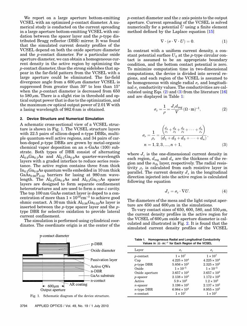
We report on a large aperture bottom-emittingVCSEL with an optimized p-contact diameter. A nu-merical study is conducted on the current spreadingin a large aperture bottom-emitting VCSEL with oxi-dation between the spacer layer and the p-type dis-tributed Bragg reflector (DBR) mirror. It was foundthat the simulated current density profiles of theVCSEL depend on both the oxide aperture diameterand the p-contact diameter. For a particular oxideaperture diameter, we can obtain a homogeneous cur-rent density in the active region by optimizing thep-contact diameter, thus the strong sidelobes that ap-pear in the far-field pattern from the VCSEL with alarge aperture could be eliminated. The far-fielddivergence angle from a 600 μm diameter VCSEL issuppressed from greater than 30° to less than 15°when the p-contact diameter is decreased from 650to 580 μm. There is a slight rise in threshold and op-tical output power that is due to the optimization, andthe maximum cw optical output power of 2:01Wwitha lasing wavelength of 982:6nm is obtained.
2. Device Structure and Numerical Simulation
A schematic cross-sectional view of a VCSEL struc-ture is shown in Fig. 1. The VCSEL structure layerswith 22.5 pairs of silicon-doped n-type DBRs, multi-ple quantum-well active regions, and 34 pairs of car-bon-doped p-type DBRs are grown by metal-organicchemical vapor deposition on an n-GaAs (100) sub-strate. Both types of DBR consist of alternatingAl0:9Ga0:1As and Al0:1Ga0:9As quarter-wavelengthlayers with a graded interface to reduce series resis-tance. The active region contains three 8nm thickIn0:2Ga0:8As quantumwells embedded in 10nm thickGaAs0:98P0:02 barriers for lasing at 980nm wave-length. The Al0:6Ga0:4As and Al0:3Ga0:7As spacerlayers are designed to form separate confinementheterostructures and are used to form a one-λ cavity.The top 100nm GaAs contact layer is doped to a con-centration of more than 1 × 1019cm−3 to achieve goodohmic contact. A 30nm thick Al0:98Ga0:02As layer isinserted between the p-type spacer layer and the p-type DBR for selective oxidation to provide lateralcurrent confinement.
The simulation is performed using cylindrical coor-dinates. The coordinate origin is at the center of the
p-contact diameter and the z axis points to the outputaperture. Current spreading of the VCSEL is solvednumerically for a potential U using a finite elementmethod defined by the Laplace equation [15]
∇ · ðσ ·∇ ·UÞ ¼ 0: ð1Þ
In contrast with a uniform current density, a con-stant potential surface U0 at the p-type circular con-tact is assumed to be an appropriate boundarycondition, and the bottom contact potential is zero.To minimize computation time in two-dimensionalcomputations, the device is divided into several re-gions, and each region of the VCSEL is assumed tobe homogeneous with single radial σr and longitudi-nal σz conductivity values. The conductivities are cal-culated using Eqs. (2) and (3) from the literature [16]and are displayed in Table 1:
σz ¼1ρ ¼ Jcdreg
VðΩ · mÞ−1; ð2Þ
σr ¼1ρr
¼
�d1ρ1 þ
d2ρ2 þ
d3ρ3 þ � � � þ dn
ρn
�
ðd1 þ d2 þ d3 þ � � � þ dnÞ;
n ¼ 1; 2; 3;…;nþ 1; ð3Þ
where Jc is the one-dimensional current density ineach region, dreg and dn are the thickness of the re-gion and the nth layer, respectively. The radial resis-tivity ρr is calculated from each resistive layer inparallel. The current density Jz in the longitudinaldirection injected into the active region is calculatedfollowing the equation
Jz ¼ σz ·∇U: ð4Þ
The diameters of the mesa and the light output aper-ture are 650 and 600 μm in the simulations.
To vary contact sizes of 650, 600, 580, and 550 μm,the current density profiles in the active region forthe VCSEL of 600 μm oxide aperture diameter is cal-culated and illustrated in Fig. 2. It is found that thesimulated current density profiles of the VCSEL
Table 1. Homogeneous Radial and Longitudinal ConductivityValues in ðΩ ·mÞ−1 for Each Region of the VCSEL
Layer σr σzp-contact 1 × 10⁷ 1 × 10⁷
Cap 4:225 × 104 4:225 × 104
p-type DBR 5:856 × 103 2:325 × 102
Oxide 1 × 10⁻⁵ 1 × 10⁻⁵
Oxide aperture 3:657 × 103 3:657 × 103
p-spacer 2:138 × 103 1:172 × 102
Active 5:9 × 10² 1:2 × 10²
n-spacer 3:198 × 103 2:137 × 102
n-type DBR 6:984 × 104 8:955 × 103
n-contact 1 × 10⁷ 1 × 10⁷Fig. 1. Schematic diagram of the device structure.
3794 APPLIED OPTICS / Vol. 49, No. 19 / 1 July 2010

depend on both the oxide aperture diameter and thep-contact diameter. For a particular oxide aperturediameter, the shape of the current density profileis determined by the size of the contact diameter.There is no significant difference in current densityprofiles at the center of the oxide aperture, but thereis an obvious drop in current density at the apertureperimeter as the contact diameter decreases from650 to 550 μm. For large contact diameters of 650and 600 μm, current crowding occurs and leads to anovershoot of carriers at the aperture perimeter, re-sulting in a ring-shaped profile in the far-field pat-tern. But for a contact diameter less than the oxideaperture diameter, the shape of the current densityprofiles is dominated by the size of the contact diam-eter rather than the oxide aperture. As illustrated inFig. 2, for small contact diameters of 550 and 580 μm,the current crowding at the aperture perimeter couldbe eliminated. So a homogeneous current distribu-tion in the active region can be expected due to opti-mization of the contact diameter.
3. Device Processing and Performance
Wet chemical etching is used to define a circularmesa. The exposed Al0:98Ga0:02As layer is oxidizedin a water vapor atmosphere using nitrogen as thecarrier gas at 420 °C to form a 600 μm diameter cur-rent aperture and to determine the active diameterof the device. After oxidation, a Si3N passivationlayer with a circular window having a 650 or 580 μmdiameter opening is deposited upon the surface andused to determine the p-contact diameter of the de-vice. A full size p-type Ti–Pt–Au contact on the top ofthe mesa is evaporated and serves as a metal pad forsoldering. The GaAs substrate is thinned to approxi-mately 120 μm to minimize absorption losses, thenpolished to an optical finish, and an antireflectioncoating of 600 μm diameter is applied to the sub-strate. Self-aligned lithography is used to evaporatethe n-type Ge–Au–Ni–Au electrical contact that sur-rounds the emission windows. The device is simplybonded to a copper heat sink with indium solder,
and the junction down bonding method is used be-cause of its efficient heat diffusion.
The comparison of far-field patterns between de-vices with 650 and 580 μm p-contact diameters is car-ried out and shown in Fig. 3. From the device with a650 μm p-contact diameter, strong sidelobes appear inthe far-field patterns under all injection current (1, 2,and 4A), as shown inFig. 3(a). Just above threshold, aring-shaped intensity profile is observed; for highercurrents, mainlobes occur at the symmetry axis butseveral sidelobes at divergence angles up to approxi-mately 30° are also present. This is the result of cur-rent crowding and leads to an overshoot of carriers atthe aperture perimeter under all injection current,resulting in a ring-shaped profile in the far-fieldpattern. The divergence angle and the amplitude ofthese sidelobes strongly depend on the injection cur-rent that is due to the appearance of different high-order transverse modes. The near-field pattern at4A is shown in the inset of Fig. 3(a). The device oper-ates at high-order transverse modes. This kind of
Fig. 2. Current density profiles for VCSEL of a 600 μm oxideaperture diameter with varying p-contact diameters.
Fig. 3. Comparison of the measured far-field pattern at differentinjection currents (I ¼ 1; 2, and 4A) between devices with 650 and580 μm p-contact diameters: dotted curve, 1 A; dashed curve, 2 A;solid curve, 4 A. (a) Devices with a 650 μm p-contact diameter;inset, near-field pattern at I ¼ 4A. (b) Devices with a 580 μm p-contact diameter; inset, near-field pattern at I ¼ 4A.
1 July 2010 / Vol. 49, No. 19 / APPLIED OPTICS 3795
optical energy distribution pattern is a disadvantagefor optical coupling output applications. Figure 3(b)shows the far-field patterns of the device witha 580 μm p-contact diameter for different lasercurrents. Themore homogeneous current density dis-tribution across the active area results in a high-quality output beam. There is no obvious strongsidelobe energy distribution observed, and the maxi-mum intensity is on the symmetry axis. The full-angleat half-maximum (FWHM) divergence angle is sup-pressed to below 15° for all the driving currents. Thenear-field pattern at 4A is shown in the inset ofFig. 3(b); the laser operates in lower-order transversemodes. Because of the circularly symmetric patternswith a low beam divergence angle, the beam of thedevice can be easily focused or collimated into a fiberin a simple butt-coupling arrangement for broadapplications.
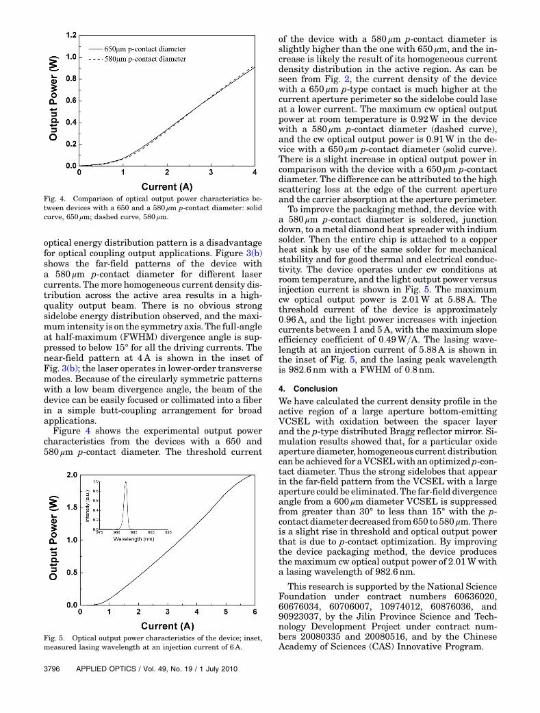
Figure 4 shows the experimental output powercharacteristics from the devices with a 650 and580 μm p-contact diameter. The threshold current
of the device with a 580 μm p-contact diameter isslightly higher than the one with 650 μm, and the in-crease is likely the result of its homogeneous currentdensity distribution in the active region. As can beseen from Fig. 2, the current density of the devicewith a 650 μm p-type contact is much higher at thecurrent aperture perimeter so the sidelobe could laseat a lower current. The maximum cw optical outputpower at room temperature is 0:92W in the devicewith a 580 μm p-contact diameter (dashed curve),and the cw optical output power is 0:91W in the de-vice with a 650 μm p-contact diameter (solid curve).There is a slight increase in optical output power incomparison with the device with a 650 μm p-contactdiameter. The difference can be attributed to the highscattering loss at the edge of the current apertureand the carrier absorption at the aperture perimeter.
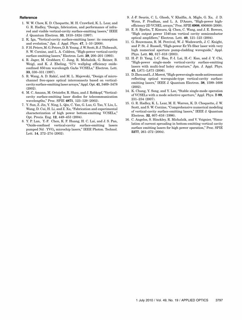
To improve the packaging method, the device witha 580 μm p-contact diameter is soldered, junctiondown, to a metal diamond heat spreader with indiumsolder. Then the entire chip is attached to a copperheat sink by use of the same solder for mechanicalstability and for good thermal and electrical conduc-tivity. The device operates under cw conditions atroom temperature, and the light output power versusinjection current is shown in Fig. 5. The maximumcw optical output power is 2:01W at 5:88A. Thethreshold current of the device is approximately0:96A, and the light power increases with injectioncurrents between 1 and 5A, with the maximum slopeefficiency coefficient of 0:49W=A. The lasing wave-length at an injection current of 5:88A is shown inthe inset of Fig. 5, and the lasing peak wavelengthis 982:6nm with a FWHM of 0:8nm.
4. Conclusion
We have calculated the current density profile in theactive region of a large aperture bottom-emittingVCSEL with oxidation between the spacer layerand the p-type distributed Bragg reflector mirror. Si-mulation results showed that, for a particular oxideaperture diameter, homogeneous current distributioncan be achieved for aVCSELwith an optimized p-con-tact diameter. Thus the strong sidelobes that appearin the far-field pattern from the VCSEL with a largeaperture could be eliminated. The far-field divergenceangle from a 600 μm diameter VCSEL is suppressedfrom greater than 30° to less than 15° with the p-contact diameter decreased from650 to580 μm.Thereis a slight rise in threshold and optical output powerthat is due to p-contact optimization. By improvingthe device packaging method, the device producesthe maximum cw optical output power of 2:01Wwitha lasing wavelength of 982:6nm.
This research is supported by the National ScienceFoundation under contract numbers 60636020,60676034, 60706007, 10974012, 60876036, and90923037, by the Jilin Province Science and Tech-nology Development Project under contract num-bers 20080335 and 20080516, and by the ChineseAcademy of Sciences (CAS) Innovative Program.
Fig. 4. Comparison of optical output power characteristics be-tween devices with a 650 and a 580 μm p-contact diameter: solidcurve, 650 μm; dashed curve, 580 μm.
Fig. 5. Optical output power characteristics of the device; inset,measured lasing wavelength at an injection current of 6A.
3796 APPLIED OPTICS / Vol. 49, No. 19 / 1 July 2010
Reference1. W. W. Chow, K. D. Choquette, M. H. Crawford, K. L. Lear, and
G. R. Hadley, “Design, fabrication, and performance of infra-red and visible vertical-cavity surface-emitting lasers,” IEEEJ. Quantum Electron. 33, 1810–1824 (1997).
2. K. Iga, “Vertical-cavity surface-emitting laser: its conceptionand evolution,” Jpn. J. Appl. Phys. 47, 1–10 (2008).
3. F.H.Peters,M.G.Peters,D.B.Young, J.W.Scott,B.J.Thibeault,S. W. Corzine, and L. A. Coldren, “High-power vertical-cavitysurface emitting lasers,” Electron. Lett. 29, 200–201 (1993).
4. R. Jager, M. Grabherr, C. Jung, R. Michalzik, G. Reiner, B.Weigl, and K. J. Ebeling, “57% wallplug efficiency oxide-confined 850nm wavelength GaAs VCSELs,” Electron. Lett.33, 330–331 (1997).
5. R. Wang, A. D. Rakić, and M. L. Majewski, “Design of micro-channel free-space optical interconnects based on vertical-cavity surface-emitting laserarrays,”Appl.Opt.41, 3469–3478(2002).
6. M. C. Amann, M. Ortsiefer, R. Shau, and J. Robkopf, “Vertical-cavity surface-emitting laser diodes for telecommunicationwavelengths,” Proc. SPIE 4871, 123–129 (2002).
7. Y. Sun, Z. Jin, Y. Ning, L. Qin, C. Yan, G. Luo, G. Tao, Y. Liu, L.Wang, D. Cui, H. Li, and Z. Xu, “Fabrication and experimentalcharacterization of high power bottom-emitting VCSELs,”Opt. Precis. Eng. 12, 449–453 (2004).
8. Y. P. Lan, Y.-F. Chen, K. F. Huang, H. C. Lai, and J. S. Pan,“Oxide-confined vertical-cavity surface-emitting laserspumped Nd : YVO4 microchip lasers,” IEEE Photon. Technol.Lett. 14, 272–274 (2002).
9. J.-F. Seurin, C. L. Ghosh, V. Khalfin, A. Miglo, G. Xu, J. D.Wynn, P. Pradhan, and L. A. D’Asaro, “High-power high-efficiency 2D VCSEL arrays,” Proc. SPIE 6908, 690808 (2008).
10. E. S. Bjorlin, T. Kimura, Q. Chen, C. Wang, and J. E. Bowers,“High output power 1540nm vertical cavity semiconductoroptical amplifiers,” Electron. Lett. 40, 121–123 (2004).
11. G. Bouwmans, R. M. Percival, W. J. Wadsworth, J. C. Knight,and P. St. J. Russell, “High-power Er:Yb fiber laser with veryhigh numerical aperture pump-cladding waveguide,” Appl.Phys. Lett. 83, 817–818 (2003).
12. H.-P. D. Yang, I.-C. Hsu, F.-I. Lai, H.-C. Kuo, and J. Y. Chi,“High-power single-mode vertical-cavity surface-emittinglasers with multi-leaf holey structure,” Jpn. J. Appl. Phys.45, L871–L873 (2006).
13. D.ZhouandL.J.Mawst,“High-powersingle-modeantiresonantreflecting optical waveguide-type vertical-cavity surface-emitting lasers,” IEEE J. Quantum Electron. 38, 1599–1606(2002).
14. K. Chang, Y. Song, and Y. Lee, “Stable single-mode operationof VCSELs with a mode selective aperture,” Appl. Phys. B 89,231–234 (2007).
15. G. R. Hadley, K. L. Lear, M. E. Warren, K. D. Choquette, J. W.Scott, and S. W. Corzine, “Comprehensive numerical modelingof vertical-cavity surface-emitting lasers,” IEEE J. QuantumElectron. 32, 607–616 (1996).
16. C. Angelos, S. Hinckley, R. Michalzik, and V. Voignier, “Simu-lation of current spreading in bottom-emitting vertical cavitysurface emitting lasers for high power operation,” Proc. SPIE5277, 261–272 (2004).
1 July 2010 / Vol. 49, No. 19 / APPLIED OPTICS 3797


![APPLICATION Plasma Processes BRIEF for VCSELs · Geography - Global Forecast to 2022” MarketsandMarkets [3] “Vertical Cavity Surface Emitting Laser (VCSELs) Market - Global Industry](https://static.fdocuments.in/doc/165x107/5f9d30cf2e8f9d72ea258e2c/application-plasma-processes-brief-for-vcsels-geography-global-forecast-to-2022a.jpg)