High Power, High Brightness Laser Diode Technology Berthold Schmidt ISLC 2008, Sorrento September...
100
High Power, High Brightness Laser Diode Technology Berthold Schmidt ISLC 2008, Sorrento September 2008
-
Upload
carlee-isom -
Category
Documents
-
view
239 -
download
7
Transcript of High Power, High Brightness Laser Diode Technology Berthold Schmidt ISLC 2008, Sorrento September...

High Power, High Brightness Laser Diode Technology
Berthold Schmidt
ISLC 2008, Sorrento
September 2008

222
My special thanks to
Boris Sverdlov, Nobert Lichtenstein,Susanne Pawlik & Gunnar Stolze (Bookham)
John Marsh, Iulian Petrescu-Prahova,Chris Baker, Stewart McDougal,
Steve Gorton (Intense)
Reinhart Poprawe (ILT Aachen)Toby Strite, Victor Rossin, Erik Zucker (JDS Uniphase)
Friedhelm Dorsch (Trumpf)
Bernd Witzigmann (ETH Zürich)Christoph Harder (Harder & Partner)
Stefan Heinemann (Fraunhofer Institut USA - Visotek)David Roh (Coherent)
Volker Krause (Laserline)
Ed Wolak, Jim Harrison, Michael Atchely(Newport Spectra)
the IEEE publishing organization .... and many more.

33
Introduction·Global photonic market view·Fields of application·Underlying technologies
·Materials for High Power Laser (HPL) Diodes
Component design for high power fiber laserand direct diode systems
·Epitaxial desin g·Waveguide design·Chip reliability and quality assessment (life testing)·S ysem t d esgn i aspecs t
Summary and outlook

44
World wide photonics market
Market segments and estimated revenuesCircled: Major application areas of High Power Laser Diodes

55
Projected Market Growth till 2015

66
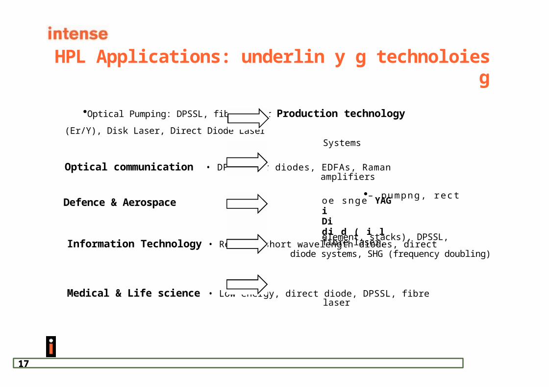
HPL Applications at a glance
·material processing, analysis, measurement Production technology
Optical communication • Data transmission, Optical amplification
Defence & Aerospace
Information Technology • Optical storage, printing, marking, display
·Aesthetics (Skin treatment,..), surgery, Medicaltherapy (PDD -Photodynamic disinfection-, PDT -therapy-,..), ophthalmology, Cancer treatment
·Communication (inter satellite,..), distance measurement, countermeasure,
target designation, Illumination, LIDAR,...

77
Production Technologies:Geometric scalin of material rocessing p g
1970 1980 1990 2000 2010Year
Which Laser for which Application?
Source: Prof. Dr. Reinhart Poprawe, ILT (AKL 2008)
102
100
10-2
10-4
10-6
-810
Drilling
Hard Materials
Engraving Tuning Marking
Micro joiningElectronics
Sheet Metal
Cutti ngMicro welding
FormingWeld ing
Electron ics Microelectronics
Semi finished Prod ucts
Optoelectronics Micro Lithography
Communication Data Processing Optical Memories
Surface TechnologyFunctional Surfaces
Micro processing
Light weight structures Automotive
Ship Building
Selective Laser
Computer chips
Remote
Hybrid
Melting
Pol ish ing
Bio-photonics
LIBS
EUV/13nm

88
Application example: welding of thin foils
Foils-Polypropylen (PP) transparent and blackthickness 100 µm
Microfluidic device- PMMA or PP sealingfoil (75 µm)
P= 1,4 –5,9 Wv= 50 to 250 mm/sd0= 70 µmdweld seam = 150 to 500 µm
Source: Prof. Dr. Reinhart Poprawe, ILT (AKL 2008)

Application example: laser polishing
Materials: 1.2343, 1.2344, 1.2316
Initial state:mille, d eroe, d dgrinded Sharp edge
maintained
1 mm
2002 2008Ra = 0,35 µm Ra = 0,09 µm
24 µ m)
Source: Prof. Dr. Reinhart Poprawe, ILT (AKL 2008)
9

101010
Application Examle p SLM of ZrO2-based Ceramics
10 mm
·Zirconium oxide (ZrO2): max. bending strength, resistance to wear and tensile strength
·Principle of Selective Laser Melting (SLM): Ceramic powder is fully molten (no sintering)
·Potential Application: Production of full-ceramic dental prostheses
SLM demo parts
Source: Prof. Dr. Reinhart Poprawe, ILT (AKL 2008)
1111
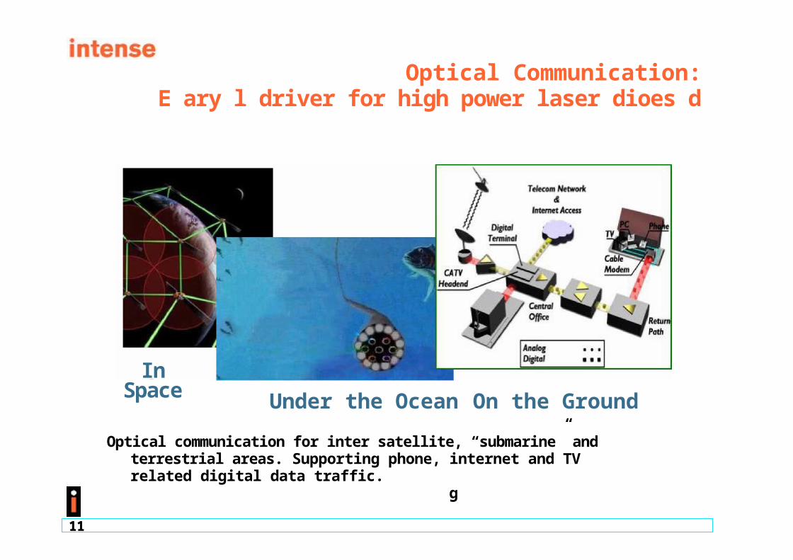
Optical Communication:E ary l driver for high power laser dioes d
Under the Ocean On the Ground
Optical communication for inter satellite, “submarine” and terrestrial areas. Supporting phone, internet and TV related digital data traffic.
g
In Space

1212
Defence and homeland security applications:slowly evolving
Laser countermeasure system against heat-seeking missilesExample: Directional Infrared Countermeasure D istance measu rement(DIRCM)
from Northrop Grumman (public Information)
,Target designation
Laser area defence system (LADS from Raytheon)(public Information)
- Laser fuses- Illumination- Detection of chemicals

1313
Information technology:optical storage, printing, display
CTP Printing - Computer to plate (CTP)Prinng ti
- Digital printing
- Display (RGB) technology - Rear projection TV

14
Medical applications:
Surgery Before After
Skin Treatment: Tattoo / Hair Removal
- Acne treatment
- Photodynamic Therapy (PDT)- Photodynamic Disinfection
(PDD)- Dental
Before After
Hair removal
Ophtalmology

15
Why choosing high power laser systemsamong other production technologies
·Processing Speed·Process Accuracy·Process Consistency·... cost (reduced cost of consumables)·Uptime (Reliability)·System flexibility·Compactness·Greener Processing (low environmentalimpact)·Enabling new fields of application
161616
Introduction·Global photonic market view·Fields of application·Underlying technologies
·Materials for High Power Laser (HPL) Diodes
Component design for high power fiber laserand direct diode systems
·Epitaxial desin g·Waveguide design·Chip reliability and quality assessment (life testing)·S ysem t d esgn i aspecs t
Summary and outlook
1717
HPL Applications: underlin y g technoloies g
·Optical Pumping: DPSSL, fibre Laser Production technology
(Er/Y), Disk Laser, Direct Diode LaserSystems
Optical communication • DFB laser diodes, EDFAs, Ramanamplifiers
Defence & Aerospace
Information Technology • Red and short wavelength diodes, directdiode systems, SHG (frequency doubling)
Medical & Life science • Low energy, direct diode, DPSSL, fibrelaser
·– pumpng, rec t oe snge YAGiDidi d ( i lelement, stacks), DPSSL, fibre laser,

1818
Laser Market Development by Laser Type
1.400
1.200
1.000
800
600
400
200
0
Laser Type
Source: Prof. Dr. Reinhart Poprawe, ILT (AKL 2008)
World Market 2007
Extrapolation of current trends to 2010
Including new applications / markets 2010

19
Underlying technologies:Erbium doped fibre amplifier (EDFA)
3 level energy sysem t when pumped with 980nm light 2
level system when pumped with 1480nm light

20www.bookham.com Page 20
Why High Power 980nm Pumps?
Typical 3-stage EDFA
E rbiu mDoped Fiber
DispersionCompensating
Fiber
GainFlattening ErbiumErbiFilter Doped Fiber Doped Fiber
um
Isolator & filter Coupler Isolator
Input Coupler
980 Pumps:·A vn : d a tage
1480 Pumps (now 980nm !):·Advantage:
Output
·Low noise figure (3 level)·Low heat load·High laser efficiency·Low cost coupler
·Un-cooled operation
·Disadvantage·Lower optical
power conversion efficiency
·higher optical conversion efficiency
·Disadvantage·Increased noise figure·More expensive coupler·High heat load, expensive cooling
High power 980 pumps enable low cost EDFAs

www.bookham.com
14xy Pump laser for Raman amplifier
Features—* Coupling to optical phonons in the glass
—* max. gain at frequency shift of 13 THz in silica (60-1 00nm)
—* broad (but not particularly flat) gain spectrumAdvantaes
g
—* Effect present in all fibers (using installed fibers)
—* Gain at any wavelength only limited by pump
source —* Low noise figure because of low ASE
—* Distributed amplification
0.0E+00
4.0E-04
8.0E-04
6.0E-04
2.0E-04
Raman Gain @ pump wavelength 1455 nm
1450 1500 15501600 1650
Wavelength (nm)
Disadvantages
—* Fast response time (no upper state lifetime
buffer) —* Pump fluctuations -> gain fluctuations ->
noise
—* Polarization dependent gain
—* High pump powers required (>200 mW)

22
Laser system desin g principles
transversally p um p ed rodlaser
INNOSLAB laser
fibre laser end-pumped
thin fibre ldisk laser
aser “Y” -pumped
All based on the same design principle requiring
·Mirrors (Cavity)·Gainmedium·Pump source
Extension...amplifier technology
Source: Prof. Dr. Reinhart Poprawe, ILT (AKL 2008)

www.bookham.com Page 23
Fibre laser pumping scheme
CP-active fiberMulti-mode pumpsFiber
com b i ne r
FBG FBG
Multi-mode pumps
Cladding pumped fiber: Yb / Er in SiO2Emission wavelength: 1.08 / 1 .53umPump wavelength at 915, 960, 975 nmPump source: Broad area single emitters / Bars Output power: ~100W -> xxkW
Fiber laseroutput optic
CP-active fiber
Single Mode Pump“Seed laser” ~1 064nm
Fiber laseroutput optic
Multi-mode pumps
Filter

Presentation title TRUMPF abbreviation - 2007/03/25 24Presentation title TRUMPF abbreviation - 2007/03/25 24Presentation title TRUMPF abbreviation - 2007/03/25 24
Rod- and Disklaser �Lamp pumped Rodlaser
Beam quality
Efficiency '
Arc lampsRod
�Diode pumped Disklaser
Laser-diodes
Disk
Beam quality
Efficiency

Presentation title TRUMPF abbreviation - 2007/03/25 25Presentation title TRUMPF abbreviation - 2007/03/25 25
Disklaser: TruDisk
TruDisk 1000 TruDisk 8002

Presentation title TRUMPF abbreviation - 2007/03/25 26Presentation title TRUMPF abbreviation - 2007/03/25 26
Design of a disklaser (8 kW)
Resonator

Parabolic Mirror
Outcoupler
Bending prisma
Laser beam
Actually: 20 passes of the pump light through the disk!
Pumping of a Disk
1 Disk
1Pump- Beam
C avy it
End-mi rror
4
5
1
8
7
2
6
3
Presentation title TRUMPF abbreviation - 2007/03/25 27

Presentation title TRUMPF abbreviation - 2007/03/25 28Presentation title TRUMPF abbreviation - 2007/03/25 28Presentation title TRUMPF abbreviation - 2007/03/25 28
> 5 kW Output Power per Disk
6000 70
0 2000 4000 6000 80000
5000
4000
3000
2000
1000
60
50
40
30
20
10
0
Pump Power Pp (W)

Presentation title TRUMPF abbreviation - 2007/03/25 29Presentation title TRUMPF abbreviation - 2007/03/25 29
TruDisk 10003 –4 disk resonator
14000
12000
10000
8000
6000
4000
2000
0
70%
60%
50%
40%
30%
20%
10%
0%
0 5000 10000 15000 20000
Pump Power Pp [W]

303030
Fiber, Disk or Direct Diode Laser?
1000Ha rd en ing
Polymer weldingB razi ng
Sold eri ng
‘SM’
fiber
Welding, sintering, surface treatment
Cladding
D ee-en etration p p
we l ding Metal cutting
Non-Metal cutting
Marking
Drilling
100
10
1
Pri nti ng
1 10 100 1000 10000
Sources:
•P. Loosen, Fraunhofer Inst. Aachen
Laser output power (W)

3131
Fiber, Disk or Direct Diode Laser? .... many applications don’t needhighest beam quality (diffraction limited beam).
Sources:
·P. Loosen, Fraunhofer Inst. Aachen·C. Harder LEOS 2006
Laser output power (W)1 10 100 1000 10000
1000HardeningPolymer welding
CladdingB r a z i n g
D ee-en etration p p
we l ding Metal cutting
200um0.22,
60um,0.22 100
Sold eri ng
Welding, sintering, surface treatment
10
P50um .0.22
ri nti ng
Non-Metal cutting
Marking
Drilling1
‘SM’
fiber
1 500um,0.22

3232
2w0
f
BPP = θ · w0
Developing trends for Lasersand their applications
2003 20081.000
100
0.1
10
1
1 10 100 1.000 10.000
Printingtherm. marking
Diode lasers(2003)
F#4 focusingoptics (NA 0,12)
soldering
lamp pumpedNd :YAG-laser
plastics welding
selective laser powder remelting
CO2-laser
brazing
metal s e e h t cutting
DPSSL
transformationhardening
melting,cleaning
deep penetration welding metals
Laser Power P [W]
Source: Prof. Dr. Reinhart Poprawe, ILT (AKL 2008)

3333
Introduction·Global photonic market view·Fields of application·Underlying technologies·Materials for High Power Laser (HPL) Diodes
Component design for high power fiber laserand direct diode systems
·Epitaxial desin g·Waveguide design·Chip reliability and quality assessment (life testing)·S ysem t d esgn i aspecs t
Summary and outlook

3434
Materials for Semiconductor Laser Processing

3535
Wavelength Range for major industrial applications /technologies requiring (red / MIR) HPL
DPSS
Med ical
Med ical
Med ical
Printing
Opticalstorage
TelcoPumps
TelcoPumps
Display,...
Laser TV Pumps & SHG
LIDAR
Fiber Laser Pumps
FiberLaserSeeds
Direct Diode Applications
Nd YAG Replacement
600nm 700nm 800nm 900nm 1000nm 1100nm 1400nm 1600nm
GaP Capability GaAs Capability InP Capability

3636
Pearls of Laser History
MOPA, SEDFB, α-DFB Tunable l
Quantum Dots,Quantum Cascade Lasers, new materials,new process technologiesnew integration technologies intercavity Lasers (SHG) monolithic Integration
asersFBG-StabilizationFlared / Taper Design Efficiency I mprovements New Waveguide Designs Materials
Laser bars / Stacks
1917 1950s 1960s 1970s 1980s 1990s 2000s 2010s
Herbert Nelson, RCA Liquid Phase Epitaxy 1962
3737
Introduction·Global photonic market view·Fields of application·Underlying technologies
·Materials for High Power Laser (HPL) Diodes
Component design for high power fiber laserand direct diode systems
·Epitaxial desin g·Waveguide design·Chip reliability and quality assessment (life testing)·S ysem t d esgn i aspecs t
Summary and outlook
3838
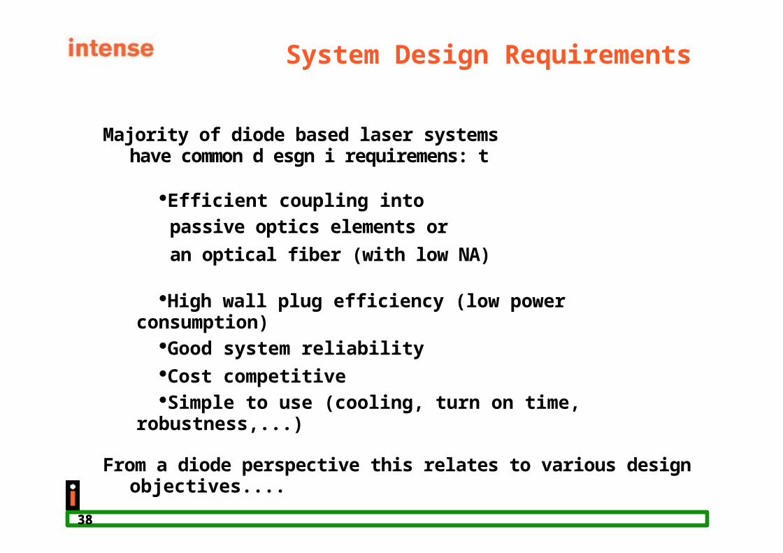
System Design Requirements
Majority of diode based laser systemshave common d esgn i requiremens: t
·Efficient coupling into
passive optics elements or
an optical fiber (with low NA)
·High wall plug efficiency (low power consumption)·Good system reliability·Cost competitive·Simple to use (cooling, turn on time, robustness,...)
From a diode perspective this relates to various designobjectives....

3939
Laser diode design targets
Common design requirements for high power laser(HPL) diodes:
·High output power·High brightness·High wall-plug and coupling efficiency(low power consumption)·High reliability + robust·Design capable for high volume manufacturing

4040
Challenges for the design of HPL
Output Power , Capacity
Robustness for Volume Manufacturing
Subsystem Design (Cost, Brightness, Reliability)
Chip Reliability (Bulk / Facet) – Quality assessment
Epitaxial Structure
Waveguide Design

4141
Challenges for the design of HPL:Wall-plug efficiency – Broad area single emitter laser
Output Power, Capacity
Key measure for high power laser diodes:
η =
WPh I I
ν η ν η ν η ν η
( )
d th dth
− ⎞
= − −⎛ ⎛
h I
⎜ ⎝ 1 ⎠ ⎟qIV qV I(wall-plug efficiency)
Others: defect density, material properties (i.e. expansion match)
Epitaxy
Design parameters:·bandgap profile, carrier
confinement·d/gamma, confinement factors·doping
profi le,·growth
processKey characteristics:·internal losses,·internal quantum
efficiency,·series resistance, laser
voltage·thermal resistance
Waveguide characteristics:·Optical
Confinement,·Vertical far f ield,·Coupling efficiency,
...

www.bookham.com Page 42
Similar laser structures with varying η ηWP
0 2 4 6 8 10
12
14
0.7
0.
6
0.5
0.40.3
0.2
0.1
0.0
WPE 1WPE 2P 1P 2
4
2
6
0
14
12
10
8
current (A)
• Device characteristics show importance of a balanced desin aroach:g pp
– Similar differential quantum efficiency
– different terminal (operating) voltages=> different doping profiles impacting wall-plug efficiency (5-6%)

434343
Differential quantum efficiency
·
η i − − injection efficiency, defined as fraction of injected carriers which are converted into optical radiation by the stimulated emission;
− physical effects controlling it are not very well established;− difficulty: carrier loss rate increases with increase of carrier
concentration (quasi-Fermi level separation), but both stabilize at threshold
=
η η ηd i ln 1 1 2
()
R R
⎛
⎜
⎝
1+
2 α i L ⎞ ⎟
1⎠
·
α − d i s t r i b u t e d l o s s α = α + α + α
i , i FC scatt. coupl.
Free carrier absorption
αp = 7 - 14⋅10-1 8p; α n = 3 - 6 ⋅ 10-18n

4444
Bandgap engineering example:Graded Index carrier confinement (GRICC)
0 . 5 1 . 0
InGaAs/AlGaAs GRICC design
·provides efficient0.8carrier confinement
·stable control of vertical waveguide·low internal losses
-1
(below 1cmreported)-1.0
Hole Quasi-Fermi Level
-1.5
Valence Band
-2.0
Vertical Position (a. u.)B. Schmidt et al. Proceedins g of SPIE Vol. 5248, SPIE, Bellinham g , WA, 2003, 42-54.
0.0
-0.5
Electron Quasi-Fermi Level
Conduction Band
0.6
0.4
0.2
0.0

4545
Low loss laser waveguides:strong guided structures
The main idea - to minimize overlap between optical mode and regions of high doping to reduce internal absorption losses
Very strong confinement undoped waveguide
M. Gokhale et al., JQE, v.33, p.2236 (1997)

4646
Low loss waveguides:Shifting mode into n material2. A symmerc t i wavegues
id
Mode maximum shifted from the QW position: lower FC absorption in QW-1
Values of aFC as low as 0.4 cmwere reported
Free carrier absorption in p material is higher than in n material: - higher absorption cross section;- higher doping for comparable conductivity required;=> The design idea is to shift optical mode from p- to n-type material
In addition higher order modes can be suppressed
M. Buda et al., JSTQE, v.3, p.173 (1997) C.M. Stikley et al., SPIE Proc., v.6104, (2006)

4747
Minimizing laser diode voltageLaser voltage V = Vj +IRs+ Vhb:
*
*·Vj - voltage on pn junction; stabilizes at threshold:
V j = F n − F p
·V hb - voltage drop on (isotype) heterojunctions throughout laser
structure:usually minimized by graded hetero-interfaces
·R s - series resistance: compromise has to be found to reconcile requiremens t of l ow d opng i f or high ηd and high d opng i f or l ow R s
M. Kanskar et al., Electron Lett, v.41, (2006)

4848
Example: Multi-mode single emitter diodefor fiber laser pumping
·793nm pump wavelength for Thulium based fiber lasers·Waveguide with ~90 um aperture·3.5 mm chip length·Achieving around 10-11 W roll over at 25 C (CW)·High wall plug efficiency

4949
Challenges for the design of HPL
Output Power , Capacity
Robustness for Volume Manufacturing
Subsystem Design (Cost, Brightness, Reliability)
Chip Reliability (Bulk / Facet) – Quality assessment
Epitaxial Structure
Waveguide Design
5050
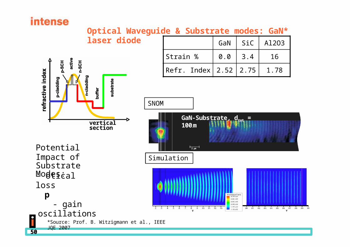
Optical Waveguide & Substrate modes: GaN* laser diodeGaN SiC Al2O3
Strain % 0.0 3.4 16
Refr. Index 2.52 2.75 1.78
SNOM
Simulation
GaN-Substrate, dtot = 100μm
2 µmPotential Impact ofSubstrate Modes:
vertical section
. . .
- otical lossp
- gain oscillations
*Source: Prof. B. Witzigmann et al., IEEE JQE 2007

www.bookham.com Page 51
Challenges for the design of HPL:Waveguide Design – single mode ridge laser
Output Power, Volume
SQW - GRICC Structure InGaAs/AlGaAs intensity profile
gain profile
Waveguide Design impacted by
·length scaling,·spatial hole burning,·local heating,·carrier injection·refractive index step (etch
depth),=> slow axis diverence linear ower near field attern
g , p ,p

52
2D simulation (*) of GaAs-based high-powerSM-Laser Diodes
- Most often 1 – 2D simulation- Solving wave equation with
changing parameters, i.e. at increased drive currents (time consuming)
- Input Parameters often not fully explored
Pictures: Boundaries and simulation domains for modeling high power laser diodes.
*Source: Prof. B. Witzigmann, ETH-Zurich

Wave guiding impacted by free carriers, etch depthand temperature...
Ridge
High waveguide stability is essential for every laser diode used for telecom-
Active region and non-telecom applications
Influenced by> Refractive index step > free carrier density> temperature variations
(thermal blooming,..)
B.Schmidt et al., Proceedings ISLC 2002
Temperatureinduced index change
53

545454
(significant higher relative increase of optical losses of 1st, 2nd and.. order modes as compared to the zero order mode)
=> suppression of coherent coupling with higher order modes (higher linear power)
Lateral Waveguide stabilizationfor high power spatial SM laser diodes
High power SM operation
> Linear Powers up to 1.9W achieved (*) > Low divergence leaky waveguide> Stabilization of fundamental mode
by increasing losses of higher order modes
* Wenzel et al., “Fundamental-Lateral Mode Stabilized RWG Lasers”, IEEE Phot. Tech. Let., Vol.20, No.3, 2008

5555
Length scaling
Both electrical and thermal resistance of the chip are inversely proportionalto the its waveguide active area;
broad area laser
V. Gaontsev et al. Proc. o SPIE v. 6104 2006 p, f (injected current (mA)

56
5670.1
2
3 4 5 6 7 12
3 4 5 6 7 10
( )zg
Asymmetric power/current distribution along the wavguidePower distribution inside laser cavityOptical intensity distri
0.8
0.6
0.4
0.2
0.0
1.0
Rfront= 0.1%Rback = 100%
0.1 0.2 0.3 0.4 0.5 0.6 0.7 0.8 0.9 1.0
cavity length (a.u.)
0.0
2520
15105
0
front facet reflectivity (percent)
=>> refractive index and gain profile changes along laser cavity
Δ F * z ⇒ N z ⇒( ) ( )
( )z*
)VΔ F
+ j z z
( ) (
ρ
( )z= +R R
spstim
j
(zRstimΓ( )
z g
=
hcS) [ ( )
( ) ]
P z P z+ + −
facetRate equations refl
ed
Voltage on laser
e
I = ∫ L j z d z
0 ( )

www.bookham.com
Challenges for the design of HPL:Waveguide Design – single mode ridge laser
0 500 1000 1500 2000 2500inected current mA j
()
Output Power, Volume
1600
1400
1200
1000
-200
400
200
800
600
0
junction side up CW-operation= °T 2 5 C
G03
G05
G07
G06
G08 >100MW/cm2
Waveguide DesignLength Scaling, Spatial hole burning, local heating, Carrier injection Refractive index, slow axis divergence

585858
Challenges for the design of HPL
Chip Reliability (Bulk / Facet) – Quality assessment
Output Power , Capacity
Robustness for Volume Manufacturing
Subsystem Design (Cost, Brightness, Reliability)
Epitaxial Structure
Waveguide Design

5959
Long term reliability & COMD protection
Catastrophic Optical Mirror Damage (COMD)
Free carrier absorption
Stimulated
E m i s s i o n A b s o r p t i o n :e-h
Non-rad iativerecombinationvia surface states
Facet Degradation leads to formation surface states Surface states cause non-radiative recombination
Non-radiative recombination leads to a local increase of current injection This leads to an increase of the local temperatureWhich causes a further shrinkage of the bandgap and thus an
increase of free carriers
Additional generation of e-h pairs leads to further absorptionof stimulated laser light causing an acceleration of the thermal run away .... COMD

6060
Avoiding COMD
Avoid or reduce formation of non-radiative recombination states ·E2
-> Cleaving in high vacuum and in-situ passivation of the cleaved surface
·Use of InGaAsP based barrier materials -> reduced oxidation (“Al-free”) -> re-growth covering cleaved facets possible
Remove formation of non-radiative recombination states ·“Cleaving on air” -> Dry etching in vacuum -> in-situ nitridation or sulphation
·“Cleaving on air” -> low energy hydrogen plasma or ion beam cleaning -> in situ passivation (ZnSe, Si,...)
M. Gasser, E.E. Latta, "Method for mirror passivation of semiconductor laser diodes," U.S. Patent No. 5063173 M. Hu, L.D. Kinney, M.
Pessa, et al.,"Aluminium-free 980-nm laser diodes for Er-doped optical fiber amplifiers," SPIE 1995, vol. 2397, 333-341
K. Hausler, N. Kirstaedter, "Method and device for passivation of the resonator end faces of semiconductor lasers based on III-V semiconductor material," U.S. Patent No. 7033852
L .. K Lindsrom, t et al."Meo th d to obtan i contamnaon i ti free laser mirrors and passivaon tiof these," U .. S Patent No. 6812152
H. Kawanishi, et al."Semiconductor laser device with a sulfur-containing film provided between the facet and the protective film," U.S. Patent No. 5208468 E.C.
Onyiriuka, M.X. Ouyang, C. E. Zah, "Passivation of semiconductor laser facets," U.S. Patent No. 6618409P. Ressel et al. "Novel Passivation Process for the Mirror Facets of Al-Free Active-Region High-Power Semiconductor Diode Lasers," PTL 2005, vol. 17, no. 5,
962-964

www.bookham.com Page 61
Long term reliability & COMD protection
E2 by Bookham: Stress test of first generation 980nm SM laser diodes
330
310
290
270
250
230
210
1901990 1991 1992 1993 1994 1995 1996 1997 1998 1999 2000 2001 2002 2003 2004 2005 2006 2007
Time (years)

626262
Avoiding COMD
Reduce number of free carriers at the laser facet
·Reduce direct carrer i injecon ti without changng i the bandgap (at wafer level process)
Front section isolation
·NAM (non absorbing mirrors) to reduce absorption, diffusion and thermalized carriers (at wafer level process)
Zn diffusion
Etching and subsequent re-growth of a III-V window Si-
doped and disordered windows
Vacancy induced windows (QWI)
B. Schmidt et al., US Patent 6782024 - High power semiconductor laser diode
H.0. Yonezu, M. Ueno, T. Kamejima and I. Hayashi, "An AIGaAs Window Structure Laser," JQE 1979, vol. 15, no. 8, 775-781J. Ungar, N. Bar-Chaim and I. Ury, "High-Power GaAlAs Window Lasers," EL 1986, vol. 22, no. 5, 279-280R .. L Thornon, t D .. F W ec, l h R .. D B urnam, h T L. Paoli and P .. S Cross, "High power (2.1 W) 10-srpe t i AlGas Alaser arrays with Si disorere d d facet windows,"
Appl Phys Lett 1986, vol. 49, no. 23, 1572-1574S. Yamamura, K. Kawasaki, K. Shigihara, Y. Ota, T. Yagi and Y. Mitsui, "Highly Reliable Ridge Waveguide 980nm Pump Lasers Suitable for Submarine and Metro
Application," OFC 2003, vol. 1, 398-399J.H. Marsh, C.J. Hamilton, "Semiconductor laser," U.S. Patent No. 6760355

6363
Effect of front section isolation *( )Standard Contact
Truncated Contact
Reduction of current injection into front section (reduced local heating)
Reduction of free carriers (impact on the gain profile)
*Source: Prof. B. Witzigmann, ETH-Zurich
6464
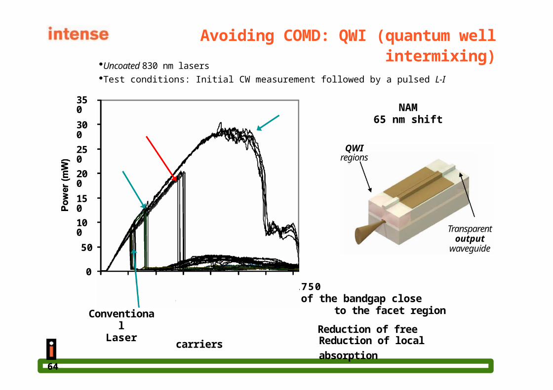
Avoiding COMD: QWI (quantum well intermixing)
·Uncoated 830 nm lasers·Test conditions: Initial CW measurement followed by a pulsed L-I
NAM45 nm shift
NAM0 nm shift
0 250 500 750 1000 1250 1500 1750Current (mA) Increase of the bandgap close
to the facet region
Reduction of free carriers Reduction of local absorption
350
300
250
200
150
100
50
0
NAM65 nm shift
QWIregions
Transparentoutput
waveguide
ConventionalLaser

6565
QWI process concept
As-grown bandgap Intermixed bandgap
Al
Ga
AlGaAs GaAs AlGaAs AlGaAs
QWI allows bandgap tuning in selected areas of the chip

6666
QWI Process StepsIntense QWI technology enables high power/brightness lasers to be produced
in a manufacturing environment·Dielectric caps are deposited on surface of wafer·W aer f i s anneae l d·Quantum wells intermix with adjacent material altering the bandgap wavelength·Wavelength change depends on properties of dielectric cap
QWI works in a variety of materials and wavelength s·808 nm SQW material used in this work
Photoluminescence spectra160
140
120
Intermixing cap Suppressing cap100
80
60
QW
20
0
700 720 740 760 780800 820 840 860
Wavelength, nm
40
Suppressed Intermixed
High TemperatureAnneal

6767
Life testing array with 64 single emitters(QWI – technology)
64 emitter life testEach device operates at 808nm with >200mW output power, room temp.

68
Challenges for the design of HPL
–
Epitaxial Structure
Waveguide Design
Subsystem Design (Cost, Brightness, Reliability)
Chip Reliability (Bulk / Facet)
Quality assessment
Robustness for Volume Manufacturing
Output Power,
Capacity

696969
Quality assessment andlife test strategies
Challenge for quality control of high power laser diodesfor industrial laser systems
·No clear industrial standards defined, yet.(in comparison to Telcordia standards for fibre networks -GR-468-)
·Different system requirements in different industries(from commodity to space application)
·Comparison of varying technologies for similar applications
Single emitter high power laser diodes (spatial multi-mode or single
mode) 1 cm High Power Laser bars with varying fill factors“Mini-Bars” and related devices
Differn e t worin d g to describe reliability (FIT, MTBF, MTTF, end of life,...)
·Additional influence factors
Mounting (Indium or hard solder (AuSn, SnAg, SnAgCu,...))
Cooling (passive cooling, active cooling (TEC, micro-channel, macro-
channel) Environment (hermetic, non-hermetic, ....)Operating regime (CW, quasi CW, pulsed)
Cost of life test equipment and test

7070
Classical life test strategy:single emitter devices
Assumptions·Known failure modes
·Laser diode lifetime follows “bath tube” curve·Infant mortality rate is vanishing or can be screened out by burn-in
·Constant failure rate (intrinsic period) is determined by sudden death (or a short wear out period followed by sudden death)·Wear out is expece t d to kick in after guaranee t d d evce i life time
a kbT)∝ x y −
·Constant failure rate can be described by: FR
I P e x p ( E
tonset

Example: Reliability testing of 980nm telecom chip
·Stress cells with different conditions (acceleration of failure rate)·high number of stress cells and devices·similar failure mode as at “field condition”·failure rate for each condition (must be constant)
·Determination of the acceleration factors in the reliability model with maximum likelihood approach (Ea , x , y)
·Prediction of reliability at use conditions: 30 - 500 FIT
0 500 1000 1500 2000Current (mA)
www.bookham.com Page 71
1200
1400 25 °C
Testi ng
1000
85 °C800
600 Use400
200
0
45 °C
°65 C

727272
Challenge of qualifying industrial devices
·High Power (single emitter) Laser Diodes are expected to operatecloser to 1 – 5kFIT at standard operating condition (in comparison tobelow 100FIT for telecom “submarine” applications)
·Acceleration of failure rates is more challenging since devicesoperate closer to the thermal roll over point at standard operatingcondition
·Cost of life testing can be significant if devices have to be tracked insitu and separately operated / cooled for conditions ranging from(10-20A, 25°-75°C heat sink temperatures)
·Operating conditions might vary severely (CW, quasi CW, pulsed)

7373
Central life test philosophy

er
– 0.15 or 0.22NA
– Rth= 2.2oC/W– rae pow10W t d
74 © 2008 JDSU. All rights reserved. SSDLTR June 2008
Example: JDSU L4 module performance & testing
·Fiber-coupled package– 105 μm diameter
– 50% wall plug 00 5 10
15 2025
Current (A)
·Laser chip InAlGaA
s–– 880-1000nm
– 100μm aperture 20
– 4.1mm cavity– AuSn solder 15
25 75%ex-ace
f
tex-fiber
15C
45%
30%
60%
15%
0%
10
5
10%
5%
0%
-5%
·Packae Testg
– 10W, 12A – T case = 35oC– 14 lasers– 0 failures -10%
0 1000 2000 3000 4000, , , ,
Time (hours)
75 © 2008 JDSU. All rights reserved. SSDLTR June 2008
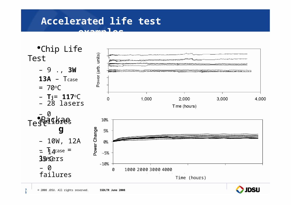
Accelerated life test examples
·Chip Life Test– 9 ., 3W 13A – Tcase = 70oC– Tj= 117oC– 28 lasers
– 0 failures

TimeZero
MechShock
85°C / 85% RH Damp Heat
Vibration
76 © 2008 JDSU. All rights reserved. SSDLTR June 2008
L4 Package qualification and robustness tests
• Reference Telcordia GR-468– ero pacage aures n u suteZ k f il if ll i
– Proves robustness of design
500G Mechanical Shock+ 20G Vibration
-10%
10%
-5%
5%
0%
18 units
0 1000 2000 30004000 5000
Time (hours)
-40°C to +85°CTemperature Cycling
-10%
10%
-5%
5%
0%
27 units
0 100 200 300 400 500
No of Cycles
10%
5%
0%
-5%
-10%12 units

Pump power trends – commercially available
10
1
L 4 6 3 9 8
L3-6 397
L3-63 96
L3-6 390
L2-6380
•
•
•
9XXnm105μm diameter fiber “Reliable” rated power
1992 1994 1996 1998 2000 20022004 2006 2008
Year
·15% annualincrease in reliable
power
·imilar trend orS f– 8XXnm–
Singlemode lasers– Multi mode lasers
– Bars
77 © 2008 JDSU. All rights reserved. SSDLTR June 2008

787878
Life t esng ti of laser dioe d bars
Important to understand
·cooling type·fill factor (FF) of bars
·operational mode (CW, pulsed, QCW)·expected degradation scheme(gradual degradation, sudden failure or a combination)·and expected failure mode(stress induced failure, contamination induced failure,COMD, bulk fail or combinaon,... ti )

7979
Types of coolers for hard solder bar mounting
(*)
- Passive Cooling (copper heat sink with heat exchanger -> Water or Air cooled)- A cve ti C oong li of high power bars (micro, meso or macro channel cooer l )
- Active cooling of single emitter devices (TEC and heat exchanger)
* Christoph Harder; “Chapter: Pump Diode Lasers”, Optical Fiber Telecommunications V A (Fifth Edition), Components and Subsystems, Editor: Ivan P. Kaminow, Tingye Li andAlan E. Willner, pp. 107-144.
Current (A)
Presentation title TRUMPF abbreviation - 2007/03/25 80
Current (A)
Presentation title TRUMPF abbreviation - 2007/03/25 80
Current (A)
Presentation title TRUMPF abbreviation - 2007/03/25 80
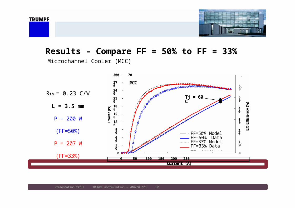
Results – Compare FF = 50% to FF = 33% �Microchannel Cooler (MCC)
Rth = 0.23 C/W
L = 3.5 mm
P = 200 W (FF=50%)
P = 207 W (FF=33%)
0 50 100 150 200250
270
300 70
MCC60
240
210 Tj = 60 C 50
40180
150
30120
FF=50% Model FF=50% Data FF=33% Model FF=33% Data
90
60
30
0
20
10
0

Current (A)
Presentation title TRUMPF abbreviation - 2007/03/25 81
Current (A)
Presentation title TRUMPF abbreviation - 2007/03/25 81
Results – Compare FF = 50% to FF = 33% �Mesochannel Compact Heat Exchanger (MesCHE)
Rth = 0.38 C/W
L = 3.5 mm
P = 127 W (FF=50%)
P = 151 W (FF=33%)
0 2 0 4 0 6 0 8 0 1 0 0 1 2 0 1 4 0 1 6 0 1 8 0 2 0 0 2 2 0
50
240 60
MesCHE
160 Tj = 60 C 40
140
120
100
80
30
20FF=50% Model FF=50% Data FF=33% Model FF=33% Data
220
200
180
60
40
20
0
10
0

828282
Life testing of laser diode bars:modes of operation
Short pulse operation I ntermittent-CW operation
Optical pulse
Current (us)
Semiconductor / Mount Temp
Mechanical stress
Current (s) GaAsα = 6 ppm/ °K
Semiconductor / Mount Temp
Mechanical stress
CuWα = 6.5ppm/ °K
Optical pulse
Cu
α = 16.5ppm/ °K
- Short pulse operation with strong variations in duty cycle and pulse length(ns - ms.... ) Application oriented (highest optical stress per pulse)
- Intermittent-CW (normally ~1 .3Hz) creates highest mechanical stress

8383
Example: QCW-Stack
HERMES QCW Stack
·10 Bar QCW Stacked Diode Arrays
·200W bars @ 808nm
·250u sec x 20Hz
·Hard solder
·MIL-SPEC
3000
2500
2000
1500
1000
500
12 %9 %
Onoin life test g g
9 %
0 -5.0E+07 0.0E+00 5.0E+07 1.0E+08 1.5E+08
2.0E+08 2.5E+08 3.0E+08 3.5E+08
Number of Shots

www.bookham.com Page 84www.bookham.com Page 84www.bookham.com Page 84
0 20 40 60 80 100 120 140 010 20 30 40 50 60 70 80 90
Drive Current [A] Current [A]
• Improved optical and electrical design– Low drive current: 60W @ 63A (50%FF) / 40W @ 42A (30%FF)– High wallplug efficiency: 53% @ 60W, 57% max WP
– Improved far field pattern: 7° x 55° (90% power)
808 BAR: High Performance in CW
160 2.5 100 2.5
140 90
802.0120 2.0
70
10060
80 1.5
50 1.5
60 40
301.040 1.0
20
2010
0.5 00 0.5

www.bookham.com Page 85www.bookham.com Page 85
Burn in Time (h] Time (h]
·Multi-cell accelerated long-term aging test – Hard-pulse (1.3 Hz, 50% duty-cycle, full ON-
OFF)·Average power wear-out <1% / 1000h (gradual
degradation) – Stability of design and proven benefits of hard
solder technology
808 BAR: Reliability assessment (Intermittent operation)
1.1 1.1
0.5
0 500 1000 1500500 1000 1500 20002500 3000 35004000
1 1
0.9 0.9
0.8 0.8
0.7 0.7
0.675W / 75A 105W / 100A0.6
0.5

868686
Challenges for the design of HPL
Output Power , Capacity
Robustness for Volume Manufacturing
Subsystem Design (Cost, Brightness, Reliability)
Chip Reliability (Bulk / Facet) – Quality assessment
Epitaxial Structure
Waveguide Design

8787
Various pumping/coupling schemes
end pumping with fiber combiner
laser bar lens
step mirror
End pumping with collimated bar,
Direct applications

8888
Cladding pumped active fiber (CP-fiber)
Special fibers for hih g power fiber laser
Low index coating (polymer with low index)
•Multi-mode waveguide (normally with high NA~0.46 to provide strong guiding of the pump light)
The high NA of the double clad fiber allows multiple low NA fiber ports to be coupe l d into one fiber and to maintan ithe brightness
Rare earth doped waveguide (normally 10-30um with 0.07 NA)

Coupling pump radiation into fiber laser
Pump radiation is usually supplied through multimode fibers with core diameter D = 50 - 105 mm and numerical aperture NA = 0.15 -0.22
P
end pumping with fiber combiner side pumping
In other words: it is impossible to increase radiance by combining radiation ofTh t d h p w p n i r e a p u i s l i d a g l i n s dseveral uncorrelated but otherwise identical sources
Fiber radiance
R ≅ α P( )2
D N Acore ×
Max. No. of pumps per node2
⎛ laser laserD N Aclad clad
× ⎞
⎜ ⎟pump pump ⎝ D N A
×
core c o re ⎠
Key objective: Optimize brightness per pump source!
89

90
Example: Second-Generation Fiber Pump Modules
·Characteristics
– Multiple emitters (e.., g a single mini-bar)
– Micro-optics for beam conditioning
– More power in (e.., g higher current at std voltage)
·Features
– Enhanced brightness per fiber channel
– Reduced thermal and electrical resistance (higher power at rollover)
– CoS with single-emitter economies, no smile
– Independent dropouts, reduced facet loading, enhance reliability
– Highly scalable at module level
H2 short presentation
90

91
Mini-Bar Fiber Pump Module• -
Brightness of industrial modules now exceeds 1 MW/cm2 sr
OrionTM series
- 20W, 105um core, 0.20NA 3.8cm
- 915nm, 940nm, 976nm 30 0.6
- mini-bar architecture25 0.5
20 0.4
- very high reliability15
03Specified Operating Pt
10
0.2
Power PCE
5 0.1
0 0
0 5 10 15 2025 30 35
Current (A)
H2 short presentation

92
Mini-Bar Reliability: verification of emitter independence
Multi-Stripe Modules as Ensembles of Semi-Independent Emitters:·failures are dominated by random, sudden failures of individual emitters
·the failure of an individual emitter only impacts other emitters by an increase in ensemble drivecurrent (for constant power) and warming of the other stripes on the same mini-bar
·all assumptions are consistent with test data giving over 300,000 hrs MTBEF (mean time between emitter failure) at the specified operating point
single-emitter failures
CoS: 5-element mini-bar on CT
(AuSn solder on CuW heatsink)
H2 short presentation
92

939393
Bar Based Direct Diode Laser Systems
Material Processing requires very high powers and powerdensities!
To achieve the required power levels the followingtechnologies are applied on system level:
·Bar multiplexing with passive optical elements
·Polarization combining
·Wavelength multiplexing

9494
Bar multiplexing to achieve highest opticalpower densities for direct application
Picture with courtesy of
9595
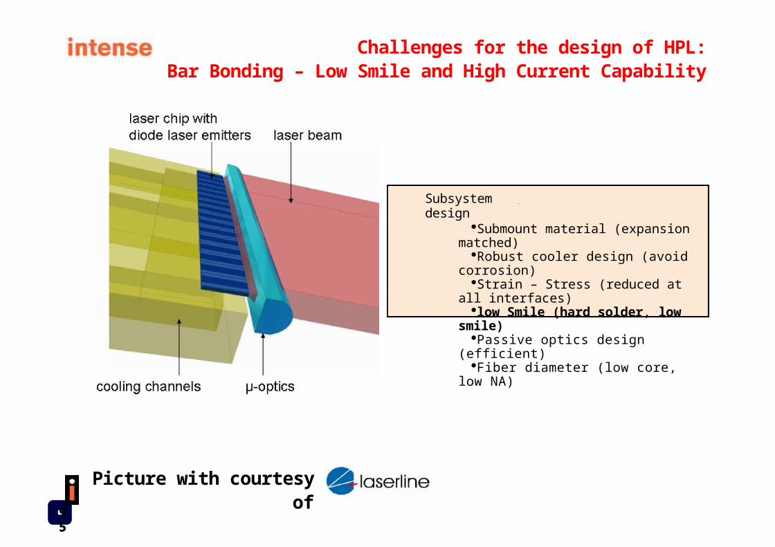
Challenges for the design of HPL:Bar Bonding – Low Smile and High Current Capability
Subsystem design
·Submount material (expansion matched)
·Robust cooler design (avoid corrosion)·Strain – Stress (reduced at all
interfaces)·low Smile (hard solder, low smile)·Passive optics design (efficient)·Fiber diameter (low core, low NA)
Picture with courtesy of

9696
Wavelength and Polarization multiplexStack 1 (interleaved 2 x 10 bars)
Output Power System: 2 X Pstack X 3 = 10kW- 12kWBPP ~ BPP (Stack) ~ 90-200 mm*mrad
λ 1 optics opticsStack 2
Polarizationcombining
λ 2 λ 3

9797
Challenes g for the desin g of HPL
Robustness for Volume Manufacturing
Subsystem Design (Cost, Brightness, Reliability)
Output Power , Capacity
Chip Reliability (Bulk / Facet) – Quality assessment
Epitaxial Structure
Waveguide Design

9898
Efficient design for robust volume manufacturing:one design platform for multiple packaging formats
TO Can forsmaller arrays
Laser Array on Ceramic Carrier
Low cost Butterfly Packageforlarger arrays
MarkingModule
Laser Array

9999
Summary and outlook
45+ years of semiconductor laser development hasbrought the technology to high level in terms of
·efficiency,·achievae bl power l eves, l·waveguide design·and reliability
Current challenges are more in the interaction with thesystem design level to optimize efficiency, brightnessand robustness of those systems
Future developments will lead to a broadening of thewavelength range, strengthening of the direct diode
laser system desins g and exploration of new fields ofapplication