High Power and High Frequency Class-DE Invertersscopeboy.com/tesla/classde.pdf · High Power and...
110
High Power and High Frequency Class-DE Inverters By Ian Douglas de Vries Thesis Presented for the Degree of DOCTOR OF PHILOSOPHY In the Department of Electrical Engineering UNIVERSITY OF CAPE TOWN August 1999
Transcript of High Power and High Frequency Class-DE Invertersscopeboy.com/tesla/classde.pdf · High Power and...

High Power and High Frequency
Class-DE Inverters
By
Ian Douglas de Vries
Thesis Presented for the Degree of
DOCTOR OF PHILOSOPHY
In the Department of Electrical Engineering
UNIVERSITY OF CAPE TOWN
August 1999

i
DECLARATION
This thesis is being submitted for the degree of Doctor of Philosophy in the department of Electrical
Engineering at the University of Cape Town. It has not been submitted before for any degree or examination at
this or any other university. The author wishes to declare that the work done in this dissertation is his own and
includes nothing that is the outcome of work done in collaboration. The author confirms that in accordance with
university rule GP7 (3) that he was the primary researcher where work described in this thesis was published
under joint authorship.
Ian Douglas de Vries16 August 1999
Email: [email protected]
Copyright © 1999, I.D. de Vries.

ii
ABSTRACT
Title: High Power and High Frequency Class-DE Inverters
This thesis investigates the various aspects of the theory, design and construction of a Class-DE type inverter
and how these affect the power and frequency limits over which a Class-DE inverter can feasibly be used to
produce AC (or RF) power. To this extent, an analysis of Class-DE operation in a half-bridge inverter is
performed. A similar approach to Hamill [6] is adopted but a different time reference was used. This allows the
concept of a conduction angle to be introduced and hence enables a more intuitive understanding of the
equations thereafter. Equations to calculate circuit element values LCR network are developed. The amount
above the resonant frequency of the LCR network that the switching frequency must be in order to obtain the
correct phase lag of the load current is shown. The effect of a non-linear output capacitance is studied and
equations are modified to take this effect into account. It was found that a Class-DE topology offers a theoretical
power advantage over a Class-E topology. However this power advantage decreases with increasing frequency
and is dependent on the output capacitance of the active switching devices. Using currently available
MOSFETs, a Class-DE topology has a theoretical power advantage over a Class-E topology up to
approximately 10MHz.
However, the practical problems of implementing a Class-DE inverter to work into the HF band are formidable.
These practical problems and the extent to which they limit the operating frequency and power of a Class-DE
type inverter are investigated. Guidelines to solving these practical problems are discussed and some novel
solutions are developed that considerably extend the feasible operating frequency and power of a Class-DE
inverter. These solutions enabled a broadband design of the control circuitry, communication-link and gate-drive
to be developed. Using these designs, a prototype broadband half-bridge inverter was developed which was
capable of switching from 50kHz through to 6MHz. When operated in the Class-DE mode, the inverter was
found to be capable of delivering a power output of over 1kW from 50kHz to 5MHz with an efficiency of over
91%. The waveforms obtained from the inverter clearly show Class-DE operation. The results of this thesis
prove that a Class-DE series resonant inverter can produce RF power up to a frequency of 5MHz with a higher
combination of power and efficiency than any other present topology. The practical problems of even higher
operating frequencies are discussed and some possible solutions suggested. The mismatched load tolerance of a
Class-DE type inverter is briefly investigated.
A Class-DE type inverter could be used for any applications requiring RF power in the HF band, such as AM or
SW transmitters, induction heating and plasma generators. The information presented in this thesis will be
useful to designers wishing to implement such an inverter. In addition a Class-DE inverter could form the first
stage of a highly efficient and high frequency DC-DC converter and the information presented here is directly
applicable to such an application.

iii
ACKNOWLEDGEMENTS
The author would like to thank the following:
• My supervisors, Mr. J.H. van Nierop for his conscientious help and for help with obtaining financial
assistance, and to Prof. J.R. Greene for his advice.
• Mr. Stephen Schrire for his advice and discussions on technical matters.
• Dr. N. Morrison for his help with confirming the Fourier analysis results.
• The University of Cape Town Research Council and ESKOM for providing part of the financial support
towards this project.
• Mr. N.O. Sokal for making the HB-Plus simulation program freely available.
• Dr. Clare Knapp, Dr. Jon Tapson, Mr. Jevon Davies and Mr. Irshad Khan for their encouragement and
everyday company and cheer.
• Professor M.K. Kazimierczuk, Dr. F.H. Raab and Dr. D.C. Hamill for their critique of this thesis.

iv
CONTENTS
TERMS AND SYMBOLS.....................................................................................................vii
1. INTRODUCTION...............................................................................................................1
1.1 BACKGROUND ................................................................................................................................... 1
1.2 THESIS OBJECTIVES.......................................................................................................................... 2
1.3 THESIS CONTENTS ............................................................................................................................ 3
2. ANALYSIS AND DESIGN EQUATIONS........................................................................4
2.1 THE CLASS-D VOLTAGE-FED SERIES RESONANT INVERTER................................................. 4
2.2 THE CLASS-DE VOLTAGE-FED SERIES RESONANT INVERTER .............................................. 9
2.2.1 Operation ................................................................................................................................... 9
2.2.2 Fundamental Component of the Midpoint Voltage ................................................................. 12
2.2.3 LCR Series Resonant Network................................................................................................ 14
2.2.4 The Effect of a Non-Linear Output Capacitance ..................................................................... 18
2.2.5 Design Example....................................................................................................................... 21
2.2.6 Other Class-DE Topologies..................................................................................................... 23
3. TOPOLOGY, SWITCHING DEVICES AND SIMULATION ....................................24
3.1 CHOICE OF THE TOPOLOGY ......................................................................................................... 24
3.2 CHOICE OF THE SWITCHING DEVICE ......................................................................................... 25
3.2.1 N-Channel Enhancement-Type MOSFET............................................................................... 25
3.2.2 Selection of the MOSFETs...................................................................................................... 27
3.3 SIMULATION OF THE INVERTER ................................................................................................. 29
3.3.1 Simulation of a Class-D Voltage-Fed Series Resonant Inverter.............................................. 29
3.3.2 Simulation of a Class-DE Voltage-Fed Series Resonant Inverter .......................................... 31
4. DRIVING THE INVERTER............................................................................................34
4.1 DRIVING THE MOSFET GATE........................................................................................................ 35
4.1.1 Requirements of the Gate-driver ............................................................................................. 35
4.1.2 Choice of the Method Used to Drive the MOSFET Gates ...................................................... 36
4.1.3 The Gate-Driver....................................................................................................................... 37
4.1.4 High and Low-side Gate-Driver Power Supplies .................................................................... 37
4.1.5 Final Gate-Drive System ......................................................................................................... 38
4.1.6 Current into MOSFET Gate when Operating in Class-DE Mode............................................ 40

v
4.2 CONTROL SIGNAL GENERATION................................................................................................. 42
4.2.1 Requirements of the Control-Signal-Generator ....................................................................... 42
4.2.2 Conceptual Circuit used for the Control-Signal-Generator ..................................................... 42
4.2.3 Final Control-Signal-Generator Circuit ................................................................................... 43
4.2.4 Possible Future Circuit ............................................................................................................ 44
5. COMMUNICATION-LINK TO THE HIGH-SIDE SWITCH ....................................45
5.1 REQUIREMENTS OF THE COMMUNICATION-LINK.................................................................. 46
5.2 METHODS OF CONTROLLING THE HIGH-SIDE SWITCH......................................................... 47
5.2.1 Pulse Transformer.................................................................................................................... 47
5.2.2 Electronic Level-Shifters ......................................................................................................... 48
5.2.3 Opto-Couplers ......................................................................................................................... 49
5.2.4 Fiber Optic Link ...................................................................................................................... 49
5.2.5 RF Modulated Carrier Signal................................................................................................... 50
5.2.6 Summary.................................................................................................................................. 50
5.3 IMPLEMENTATION OF A FIBER OPTIC COMMUNICATION-LINK......................................... 51
5.3.1 LED Transmitter Drive Circuit................................................................................................ 51
5.3.2 Comparator .............................................................................................................................. 54
5.4 CONCLUSIONS.................................................................................................................................. 56
5.5 DISCUSSION ...................................................................................................................................... 56
6. PHYSICAL CONSTRUCTION OF THE INVERTER ................................................57
6.1 DESIGN CONSIDERATIONS OF THE INVERTER CONSTRUCTION ........................................ 57
6.2 ACTUAL CONSTRUCTION OF THE INVERTER .......................................................................... 59
6.3 RESONANT LOAD NETWORK ....................................................................................................... 62
6.4 MEASUREMENTS............................................................................................................................. 63
6.5 OVERVIEW OF THE WHOLE INVERTER...................................................................................... 64
7. EXPERIMENTAL RESULTS.........................................................................................65
7.1 TUNING PROCEDURE FOR CLASS-DE OPERATION ................................................................. 66
7.2 OPERATING WAVEFORMS, POWER OUTPUT AND EFFICIENCY OF THE INVERTER ....... 72

vi
8. MISMATCHED LOAD TOLERANCE..........................................................................81
8.1 IDEAL CLASS-D INVERTER ........................................................................................................... 82
8.2 PRACTICAL CLASS-D INVERTER ................................................................................................. 83
8.3 THE CLASS-DE INVERTER ............................................................................................................. 84
9. CONCLUSIONS................................................................................................................87
9.1 CLASS-DE VERSUS CLASS-E ......................................................................................................... 89
9.2 ORIGINAL WORK ............................................................................................................................. 90
APPENDIX A. Fundamental Component of the Midpoint Voltage..............................91
APPENDIX B. HB-Plus Simulation Results of the Design Example.............................93
APPENDIX C. Circuit Diagrams......................................................................................95
C.1 DRIVE-SIGNAL-GENERATOR CIRCUIT ....................................................................................... 95
C.2 GATE-DRIVER CIRCUIT.................................................................................................................. 96
APPENDIX D. Design Equations of a Half-Bridge Class-DE Inverter ........................97
REFERENCES.......................................................................................................................99

vii
TERMS AND SYMBOLS
Various means of producing RF power are often referred to as RF Amplifiers in the literature. The use of
Inverter rather than Amplifier has been adopted here when applied to Class-D, Class-DE and Class-E topologies
as these actually convert electrical power from DC to RF and do not amplify a signal as such.
TERMS
Midpoint - The common point connecting the high and low-side switches of a half-bridge inverter.
Midpoint voltage - The voltage of the midpoint referenced to ground.
Load Current - Current out of the midpoint and into the load (i.e. into the LCR network).
Switching Frequency - The frequency the inverter is being driven at (also referred to as the driving frequency
or operating frequency).
Switching Period - The inverse of the switching frequency.
Conduction Angle - The angular portion of a full switching period over which the switch is fully on.
On-time - The time the switch is on for in one switching period (related to the conduction angle)
Dead-time - The time difference between one half of a switching period and the on-time.
Drive-signal - The signal that controls the switch state (i.e On or Off)
SYMBOLS
fs Switching frequency
Ts Switching period
sω Angular switching frequency
vm(t) Time varying midpoint voltage
iL(t) Time varying load current
Ip Peak value of the load current
Vs The supply voltage (rail to rail potential difference)
φ Conduction Angle of Switches
ton On-time
td Dead-time
Co The output capacitance of the switching device
Qo The total charge removed from the midpoint during the dead-time by the load current
S1 High-side switch of the half-bridge inverter
S2 Low-side switch of the half-bridge inverter
vS1(t) The time varying voltage across the high-side switch, S1
iS1(t) The time varying current through the high-side switch, S1
iC1(t) The time varying current through the high-side switch's output capacitance

viii
vo(t) The time varying voltage across the load resistance
1V The Fourier series coefficient of the fundamental component of the midpoint voltage
vm1(t) The fundamental component of the midpoint voltage
α The phase angle between the fundamental component of the midpoint voltage and the load current
Pout RF Power output of the inverter
IS-avg The average current through each switch
IS-rms The RMS current through each switch
Q The loaded quality factor of a series LCR network
U Switch Utilization factor
n Number of switches used in the topology
rω Natural resonant frequency of a resonant circuit
Z The Effective Load Impedance
X The reactance of the effective load impedance
R Resistance
L Inductance
C Capacitance
QT Total charge needed to charge the output capacitance of a MOSFET to a specified voltage VDS
Co-eff The effective output capacitance of a MOSFET at a particular supply voltage
Vdri Supply voltage to the gate-driver output stage
η Efficiency

1
CHAPTER 1. INTRODUCTION
1.1 BACKGROUND
Radio frequency (RF) power is widely used in industry for a variety of applications such as induction heating,
dielectric heating and plasma generation. The majority of these applications generally require RF power at a
single frequency, ranging from the tens of kHz through to 27 MHz. The power levels needed range from watts
to MW, with the majority of applications requiring a few kW. The RF power sources providing the RF power
needed for these applications use a variety of different types of topologies and active devices. The basic function
required of a RF power source for these applications is to produce AC power at a single frequency from a DC
input source, as shown in Figure 1.1. Various methods of producing this RF power are briefly described below.
Pre-1980, triode valve oscillators were traditionally used to produce the RF power, and had a typical efficiency
of approximately 60-65% [16]. As valves have a very large power dissipation capability, they are still the only
means of producing power levels of more than 10 kW above a few MHz. However, valve oscillators have a
number of disadvantages, which lead to the development of a number of different types of solid-state power
sources, over the last two decades, for the various frequency ranges. Solid-state power sources offer numerous
advantages over valve sources, such as the stability and control of the output power, repeatability, smaller size
and weight, lower operating voltages, higher efficiency and a longer lifetime. For these reasons, solid-state
power sources are required for many applications and have become widely used.
These solid-state sources employ a variety of different topologies depending on the application, frequency and
power [2,16,17,55]. Traditionally, many of the HF solid-state power sources operated in a linear Class-B or
Class-C mode. The problem with linear topologies is that the active device is used as a linear current source.
This limits the theoretical efficiency of linear topologies, e.g. a Class-B amplifier delivering a full-output
sinusoidal waveform into a pure resistive load will have a theoretical efficiency of 78.5%. In practice they have
typical efficiencies of only 55-65%. This limits for the power output of a solid-state linear topology as
transistors have poor power dissipation capabilities compared to valves. Thus for high power single frequency
applications, efficiency is a priority concern in a solid state source.
To improve efficiency and increase the power output of a solid-state RF power source, one could switch the
active devices on and off in a switch mode topology. An essential requirement of switching the active devices at
INVERTER(RF Power Source)
AC OutputPower
(At required frequency)
DC InputPower
Figure 1.1 Basic function of an RF power Source

Chapter 1. Introduction 2
very high frequency is low switching losses. Various resonant mode type topologies exist that achieve low
switching losses by employing zero current and/or zero voltage switching transitions. Of these, the most suitable
resonant converter topologies for operation at very high frequency are the Class-D voltage-fed series resonant
inverter, Class-E and more recently the Class-DE voltage-fed series resonant inverter [5,6,7,27].
Class-D switching type power sources are available for power levels of up to hundreds of kW and at frequencies
approaching 1 MHz. At frequencies above 1 MHz, a Class-D type inverter suffers from practical
implementation difficulties and its efficiency decreases as it starts to suffer from capacitive switching loss due to
the parasitic output capacitances of the switching devices. These effects worsen with increasing voltage and
frequency. These facts have limited the applications of relatively high power Class-D type topologies at
frequencies higher than 1 MHz [3,5,6,7,47,48].
Class-E is a tuned single ended switching inverter that can operate at these frequencies with good efficiency [4].
It has zero voltage, zero dv/dt (zero load current) switching conditions and hence does not suffer from the
switching loss of Class-D. It is also a single ended topology and hence the gate drive is much simpler to achieve
than a two-switch Class-D. High frequency operation of a Class-E inverter has been shown to be feasible and
commercial solid-state Class-E power sources are available up to power levels of 10 kW in the HF band.
However, a Class-E topology has one main disadvantage over a Class-D circuit, in that its switch utilization
factor is 0.098 and that of a Class-D is 0.159. This theoretically enables a Class-D circuit to produce 62% more
power than a Class-E with the same current and voltage stresses on their switches.
Class-DE offers some of the better features of Class-D and Class-E. It is based on a Class-D voltage-fed series
resonant inverter, but it employs the zero-voltage and zero-load-current turn-on transitions associated with a
Class-E topology, and it has a switch utilization factor approaching that of a Class-D (0.159). Operating a
voltage-fed series resonant circuit in the Class-DE mode effectively eliminates the capacitive switching losses
and hence enables operation at higher frequencies [5,6,7].
1.2 THESIS OBJECTIVES
The aim of this thesis was to investigate the various aspects of the theory, design and construction of a Class-DE
type inverter and how these affect the power and frequency limits over which a Class-DE inverter can feasibly
be used to produce RF power. To this extent an analysis and a description of Class-DE operation was
undertaken with the intent of developing simple and intuitive design equations. The effect of the non-linear
output capacitance was investigated and found to be considerable and hence the equations were adapted to take
this effect into account. It was found that a Class-DE topology, using current power MOSFETs, offers a
theoretical power advantage over a Class-E topology up to approximately 10 MHz, depending on the output
capacitance of the switching MOSFET. However, an investigation into the technical aspects of implementing a
Class-DE inverter to work up to this frequency were found to be formidable and to a large extent these technical
problems have limited the practical applications of half-bridge inverters to less than 1 MHz. Aspects of these
technical problems and guidelines to solving them are discussed. Areas that could be improved were

Chapter 1. Introduction 3
investigated and some novel solutions were developed that considerably extended the feasible operating
frequency of a high power half-bridge inverter. Using these solutions, the development of prototype voltage-fed
half-bridge series resonant inverter that could operate in Class-DE mode was undertaken. An initial target of 1
kW at 5 MHz was thought to be feasible. Some of the practical problems of even higher operating frequencies
are discussed and some possible solutions suggested.
An isolated DC-DC converter basically consists of an inverter producing AC power from a DC power input, the
AC power is then fed into a transformer, followed by a rectifier. A method of regulating the power flow through
the inverter is used to maintain the correct DC output voltage. The desirable characteristics of an inverter used in
a DC-DC converter are; high efficiency, high frequency, low EMI and a good switch utilization factor. A
Class-DE inverter can potentially achieve very high efficiency at high frequencies (>1 MHz) with low switching
losses, a good switch utilization factor, no turn-on current spikes and hence very low radiated EMI. This makes
it a very attractive inverter for use in DC-DC converters. The design and construction of a Class-DE inverter is
essentially the same whether the RF output is rectified into a DC voltage, or fed into a load, as shown in Figure
1.1. The issues investigated in this thesis will therefore be of directly applicable to designers when
implementing a Class-DE type inverter in a DC-DC converter.
1.3 THESIS CONTENTS
Chapter 2 provides a description and an analysis of Class-DE operation. Design equations for calculating circuit
element values are developed. The effect of a non-linear output capacitance is studied and the design equations
are modified to take this effect into account. Chapter 3 deals with some of the aspects of implementing a real
inverter, such as the choice of topology and the choice of the switching devices. Simulations of the inverter with
the selected MOSFETs and topology are then performed. Chapter 4 investigates the various aspects of
controlling the inverter in order to achieve Class-DE operation. These include driving the gate capacitance to
achieve the required switching times and generation of the control signals for the high and low-side MOSFETs.
Chapter 5 provides a summary of the various methods of controlling the high-side switch. A fiber optic
communication-link is demonstrated to be the optimal choice, and a fiber optic link to control the high-side
switch is developed. Chapter 6 investigates the aspects that affect the high frequency performance of a half-
bridge inverter and deals with the design of the physical construction of the inverter. Chapter 7 presents the
operating waveforms and results of the prototype inverter at various frequencies and powers. Chapter 8
investigates the effect of a mismatched load on the operation of the inverter and the factors affecting the
tolerance of the inverter to mismatched loads. Conclusions drawn from the work and results presented in this
thesis are given in chapter 9. Appendix A gives the derivation of the fundamental component of the midpoint
voltage. Appendix B shows the HB-Plus simulation results of the theoretical design example given in chapter 2.
Appendix C provides the circuit schematics of the various circuits used throughout the thesis. Appendix D gives
a summary of the design equations for a Class-DE inverter developed in this thesis.
4
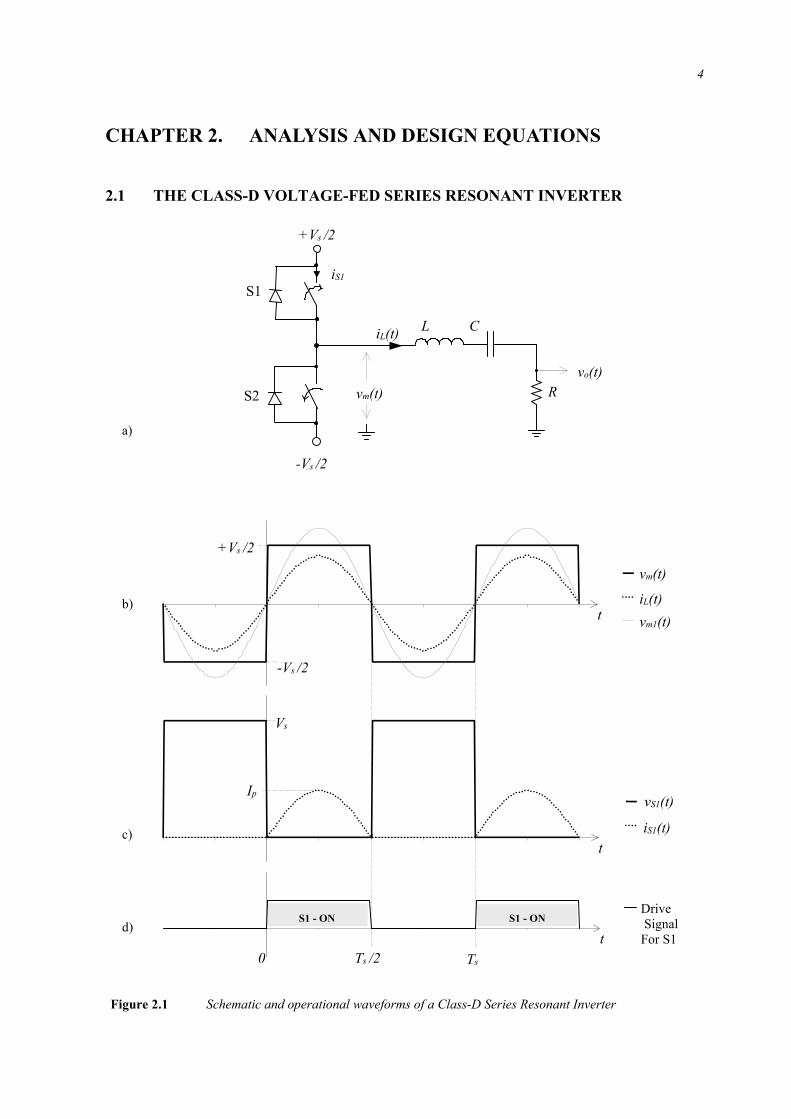
CHAPTER 2. ANALYSIS AND DESIGN EQUATIONS
2.1 THE CLASS-D VOLTAGE-FED SERIES RESONANT INVERTER
a)
b)
c)
d)
+Vs /2
-Vs /2
Vs
Ip
S1 - ONS1 - ON
TsTs /20
vm(t)
Drive SignalFor S1
iS1
L C
R
-Vs /2
+Vs /2
S1
S2
t iL(t) vm1(t)
vS1(t)
iS1(t)t
t
vm(t)
iL(t)
vo(t)
Figure 2.1 Schematic and operational waveforms of a Class-D Series Resonant Inverter

Chapter 2. Analysis and Design Equations 5
The classic Class-D voltage-fed half-bridge series resonant inverter was first introduced by Baxandall [1] and is
given in Figure 2.1. It consists of a voltage-fed half-bridge inverter with a series LCR circuit added to the
midpoint. The transfer function of this LCR network between the input at the inductor and the output across the
resistor is given by
CjLjR
RjH
ωω
ω1
)(++
= (2.1.1)
The natural resonant frequency, rω , and loaded quality factor, Q, of the LCR circuit are given by
a)LCr1=ω b)
RLQ rω
= (2.1.2)
An analysis of the Class-D operation begins by assuming the switches are ideal with zero switching times, no
on-resistance and no parasitic capacitance [1,2,3]. As MOSFETs are the primary switching devices that are used
in high frequency converters, an ideal diode is put in parallel with each switch to model the internal diode of the
MOSFET. It is also assumed that all the components of the tuned LCR resonant network are lossless, time
invariant and linear. For Class-D operation, the high and low-side switches of the half-bridge are alternately
switched on and off with a 50% duty cycle. The mid-point voltage, vm(t), will therefore be a symmetrical square
wave of amplitude Vs /2 as shown in Figure 2.1 (b). The Fourier series representation of vm(t) is then
).....5sin(52)3sin(
32)sin(2)( tVtVtVtv ssssssm ω
πω
πω
π++= (2.1.3)
where sω is the switching frequency (also referred to as the operating frequency or driving frequency) of the
half-bridge inverter.
The switching frequency, sω , of the inverter is set equal to the resonant frequency, rω , of the LCR network, to
obtain tuned series resonant operation. When this is the case, to find the output voltage across the load resistor,
we must examine the Fourier series of the midpoint voltage and transfer function of the LCR network. The
normalized moduli of the midpoint voltage’s frequency spectrum, | )(ωmV |, and the transfer function, | )( ωjH |,
are plotted in Figure 2.2. The frequency spectrum of the output voltage is the product of )(ωmV and )( ωjH .
The Dirac deltas of )(ωmV thus sample the frequency response of )( ωjH at their respective frequencies. At
the resonant frequency of the LCR circuit, the transfer function )( ωjH simply equals one. Thus the
fundamental component of midpoint voltage, referred to as vm1(t), will be transmitted with no amplitude or
phase change. To find the amplitude of the next most significant harmonic, namely the third, we must evaluate
the transfer function at rωω 3= . This can be done by using the following substitution,
CLQR
rr ω
ω 1== . (2.1.4)

Chapter 2. Analysis and Design Equations 6
Thus evaluating the transfer function at rωω 3= and using the substitutions of equation (2.1.4) we have
QjjH r 83
3)3(+
=ω (2.1.5)
and2649
3)3(Q
jH r+
=ω (2.1.6)
From the Fourier series of the midpoint voltage we know that the amplitude of the third harmonic will be one
third that of the fundamental. Hence the ratio of the of the third harmonic to the fundamental in the output
voltage can now be found using equation (2.1.6), giving
21
3
649
1
QVV
m
m
+= (2.1.7)
For a Q of 3, the ratio of the third harmonic to the fundamental is 4%. All higher harmonics will be reduced to
an amplitude considerably less than this. The amount of harmonic content that can be tolerated depends on the
application and is at the discretion of the designer. For the subsequent analysis, the Q will be assumed to be high
enough to reduce all the harmonics to a negligible amount. The output voltage, vo(t), will then simply be the
fundamental component of midpoint voltage, referred to as vm1(t), given by
)sin(2
)()( tV
tvtv ss
m1o ωπ
== . (2.1.8)
The fundamental component of the midpoint voltage, vm1(t), which is also the output voltage, vo(t), can be seen
in Figure 2.1 (b).
1/51/3
1
0
0.2
0.4
0.6
0.8
1
0 1 2 3 4 5
Normalized Frequency
|,)(| ωjH
|)(| ωmV
Q =3
ωs , ωr
Figure 2.2 Frequency Spectrum of the Midpoint Voltage and Transfer Function of LCR tuned Circuit

Chapter 2. Analysis and Design Equations 7
The current out of the midpoint and into the LCR network (referred to as the load current) will be the same as
the current through the load resistor. The current through the load resistor is determined by the output voltage
across it and will therefore be a sinusoid in phase with the driving voltage, as shown in Figure 2.1 (b), given by
)sin()sin(2)(
)( tItR
VR
tvti sps
soL ωω
π=== (2.1.9)
whereRV
I sp π
2= (2.1.10)
The load current is alternately conducted by each switch for half a period. The current through each switch when
it is on is thus a half sinusoid with a peak value of Ip. When the switch is off the voltage across it will be the rail
to rail potential difference, Vs. This can be seen in Figure 2.1 (c), which shows the voltage across the high side
switch S1, vS1(t), and the current through it, iS1(t). The average current, IS-avg, and the RMS current, IS-rms,
through each switch are then
a)π
pavgS
II =− b)
2p
rmsS
II =− (2.1.11)
The power output, Pout, delivered to the load resistance is
RVRI
P spout 2
22 22 π
== (2.1.12)
An alternative way to calculate the power output is to multiply the average current delivered through each
switch from the supply to the midpoint, by the supply voltage. Thus the output power can also be expressed as
πps
out
IVP = (2.1.13)
This method will be used in later power output calculations. The switch utilization factor, U, for switches used
in a Class-D topology is defined by the following equation,
π21==
pp
out
IVnP
U (2.1.14)
where Pout is the power output of the inverter, n is the number of switches used and Vp and Ip are the peak
voltage and current imposed stresses on each switch.. For the classic Class-D inverter 159.021 == πU ,
when the maximum peak current is used in the calculation. A perfect converter topology with the highest
possible switch utilization factor would have a square voltage and current imposed on its switches [3]. It has a
switch utilization factor of U = 0.25, to which Class-D compares favorably.

Chapter 2. Analysis and Design Equations 8
If the switching devices are MOSFETS however, it is more meaningful to use the maximum permissible RMS
current to calculate the switch utilization factor, which then gives the ideal converter a switch utilization factor
of U = 0.354. Using the maximum permissible RMS current to calculate the switch utilization factor for a
Class-D topology, gives it a switch utilization factor of U = 0.318. The Class-D series resonant inverter would
then compare very favorably to the ideal topology.
In Figure 2.1 (c) it can be seen that each switch never simultaneously has voltage across it and current through
it. Ideally this would mean that no power is dissipated in the switches and the efficiency is theoretically 100%.
However, each switch turns on at zero-load-current but must swing the midpoint voltage from one rail to the
other instantaneously. In practice this is impossible, as each switching device has an output capacitance. The
switch turning on will have to discharge its own capacitance and charge the other device’s capacitance from one
supply rail to the other. This will cause a capacitive energy loss during each switching transition and hence the
total power loss, PD, will be proportional to the switching frequency and is given by the expression,
ssoD fVCP 22= (2.1.15)
where Co is the output capacitance of each switch, and fs is the switching frequency of the inverter. To calculate
a more realistic power loss when using MOSFETs with a non-linear output capacitance, it will be more practical
to use the effective output capacitance in equation (2.1.15) defined later in the text in section 2.2.4. However,
from equation (2.1.15) we can see the power dissipation increases with increasing switching frequency and
hence the efficiency of a Class-D series resonant inverter will therefore decrease with increasing operating
frequencies.

Chapter 2. Analysis and Design Equations 9
2.2 THE CLASS-DE VOLTAGE-FED SERIES RESONANT INVERTER
2.2.1 Operation
Figure 2.3 (a) shows a voltage-fed half-bridge series resonant inverter with each switch having an output
capacitance, Co. All components are assumed to be ideal and time invariant. The inverter is operated in a similar
manner to a Class-D inverter but with some key differences in order to achieve Class-DE type operation, which
are now elaborated upon. The capacitive switching losses present in classic Class-D operation can be reduced by
simply operating the inverter above the resonant frequency of the tuned circuit and reducing the conduction
angle of the switches i.e. reducing the duty cycle below 50%, [3]. If the switching frequency of the inverter is
above the resonant frequency of the LCR network, the load will look inductive and hence the load current will
be lagging the (driving) midpoint voltage. The Q of the series resonant is assumed to be high enough to force
the load current to be sinusoidal and the harmonic content negligible. The phase lag of the load current and the
conduction angle of the switches can be actually be adjusted until each switch turns on when the load current is
zero and there is zero voltage across it. The mechanism of operation may be described by the following
sequence of events:
The conducting switch will turn off before the current through it has completed a half sinusoid. This current will
then be diverted into the two output capacitances and start to charge them, and thus the midpoint voltage will
swing towards the opposite rail. One output capacitance will be charging and the other will be discharging. The
curve traced out by the midpoint voltage as it swings from one rail to the other during the dead-time will be the
last part of a sinusoidal waveform. If the phase lag and dead-time are correct, then the midpoint voltage should
reach the opposite rail as the load current reaches zero. The opposing switch now turns on with zero voltage
across it and as the load current is zero, there will be zero dv/dt across the switch and zero current through it.
The switch therefore will not have to conduct any load current as it turns on. Hence zero-voltage and
zero-load-current turn-on is achieved [27,5,6,7]. This will give Class-E switching conditions in a traditional
Class-D topology and thus this method of operation has been termed Class-DE [7]. The energy stored in the
output capacitances is simply oscillated from one to the other with no power dissipation occurring. These effects
can be seen in the waveforms of Figure 2.3. Class-DE effectively utilizes the intrinsic output capacitances of the
switching devices as loss-less snubbers and hence this method of operation is theoretically 100% efficient.
If the load current is defined as,
)sin()( tIti spL ω= (2.2.1)
and the inverter is operated in Class-DE mode, then the waveforms shown in Figure 2.3 are obtained. Shown in
Figure 2.3 (b) is the midpoint voltage, vm(t), the current out of the midpoint, iL(t), and the fundamental
component of the midpoint voltage, vm1(t). Figure 2.3 (c) shows the voltage across, vS1(t), and the current
through, iS1(t), the high side switch, S1. Figure 2.3 (d) shows the current through the high side switch’s output
capacitance, iC1(t). The voltage and current waveforms for S2 are identical to those of S1 but are phase shifted
by exactly 180o.
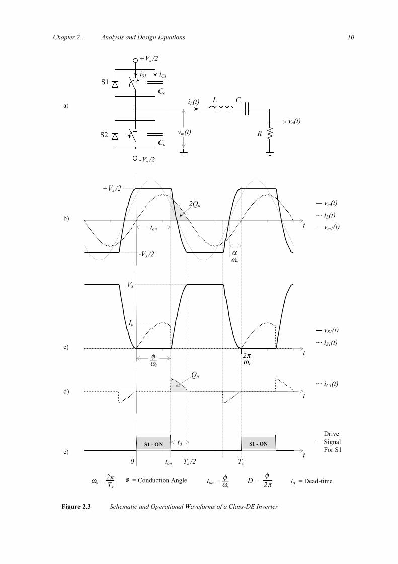
Chapter 2. Analysis and Design Equations 10
L C
R
iL(t)
S2
iS1
+Vs /2
S1Co
a)
Figure 2.3 Schematic and Operational Waveforms of a Class-DE Inverter
d)
c)
b)
e)Ts /2ton
ωs
φ
DriveSignalFor S1
0
Qo
= Conduction Angleφ2πφ
D =
ωs2π t
t
t
tS1 - ON S1 - ON
iC1
Co
-Vs /2
vm(t) vo(t)
vm(t)
iL(t) vm1(t)
+Vs /2
-Vs /2
Vs
ton
2Qo
Ip vS1(t)
iS1(t)
iC1(t)
Ts
td
ωs
φton =ωs = 2πTs
td = Dead-time
ωs
α

Chapter 2. Analysis and Design Equations 11
The analysis of Class-DE operation begins by examining the conditions under which zero-voltage and zero-
load-current turn-on is achieved. In order to achieve zero-voltage and zero-load-current turn-on, the total charge,
2Qo, removed from midpoint by the load current during the dead-time must equal the total charge required to
charge both output capacitances through a voltage of Vs. To calculate the conduction angle (or duty-cycle, D)
required to obtain this, these two are equated, giving
soo VCQ 22 =
Expanding for 2Qo sosp VCdttIs
s
2)sin( =∫ωπ
ωφω (2.2.2)
This can be solved for cosφ giving
12
cos −=p
sos
IVCω
φ [ ]πφ ,0∈ (2.2.3)
The conduction angle of the switches can vary from zero to a maximum value of 180o. A conduction angle of
180o represents the classic Class-D operation. The maximum frequency of operation for a given Ip and Co is
obtained when the conduction angle approaches its minimum value (i.e. zero). Setting the conduction angle to
zero gives a maximum operating frequency of
so
p
VCI
=maxω (2.2.4)
Thus for high-frequency operation, a high ratio of Ip /Vs and a low output capacitance, Co, are preferable. A
more realistic minimum conduction angle of 90o gives a maximum operating frequency of half of the above. The
above expression is only valid for Class-DE operation. Higher frequencies can be achieved if capacitive
switching losses are allowed.
The average current through each switch for a conduction angle of φ may be expressed as
dttIT
Iont
sps
avgS ∫=−0
)sin(1 ω
( )φπ
cos12
−= pI(2.2.5)
The RMS current through each switch for a conduction angle of φ is
dttIT
Iont
sps
rmsS ∫=−0
22 )(sin1 ω
πφφ
2)2sin2(
2−
= pI(2.2.6)

Chapter 2. Analysis and Design Equations 12
Apart from the usual ratings of a switch, another specification is of importance at high frequencies and pertains
to the maximum allowed rate of change of voltage across the switch. The maximum voltage slew rate (dv/dt)
imposed on a switch occurs at the instant of its turn off. At this point the load current has a value of Ip sinφ and
it is all being diverted into the two output capacitances, thus using dv/dt = I /C, we have
φsin2 o
p
MAX CI
dtdv = (2.2.7)
At operating frequencies considerably lower than the upper limit of the MOSFET, discrete capacitance may be
added to the midpoint to increase Co, hence lowering the dv/dt and reducing the amount of EMI produced.
The power output of the inverter can be calculated by multiplying the average current delivered through each
switch by the supply voltage, giving
( )φπ
cos12
−= psout
IVP (2.2.8)
From this equation, it can be seen that power flow through the inverter may be controlled by varying the
conduction angle. As the conduction angle is varied from 180º to zero, the power output will be reduced from its
maximum value down to zero. This should be useful in such applications as DC-DC converters.
The switch utilization factor, U, of Class-DE operation depends on the conduction angle and is given below
( )φπ
cos141 −==
pp
out
IVnP
U (2.2.9)
The switch utilization factor approaches that of a Class-D topology (0.159), as the conduction angle approaches
180º. For a conduction angle of 90º, the switch utilization factor is 0.08.
2.2.2 Fundamental Component of the Midpoint Voltage
The path the midpoint voltage traces out during the first dead-time will be a part of a sinusoid and is given by
KdttIC
tv spo
m +−= ∫ )sin(2
1)( ω [ ]2, son Ttt ∈ (2.2.10)
Integrating and using the boundary condition that 2)( sonm Vtv = , gives
+−+
+=
φφω
φ cos1cos1
2)cos(
)cos1()( s
ss
mV
tV
tv [ ]2, son Ttt ∈ (2.2.11)
A similar result can be obtained for the path the midpoint voltage traces out during the second dead-time. The
midpoint voltage is thus defined for a full period and its fundamental component can be found using Fourier
analysis. If a complex exponential Fourier series representation of the midpoint voltage is used, the positive
coefficient of the fundamental component is shown in Appendix A to be

Chapter 2. Analysis and Design Equations 13
( )[ ]φφφφπφπ
21 sincossin
)cos1(2j
VV s −+−
+= (2.2.12)
The fundamental component, vm1(t), of the midpoint voltage, vm(t), is then shown in Appendix A to be given by
)cos(2)( 1 βω += tVtv sm1 (2.2.13)
where φφφφπφπ
421 sin)cossin(
)cos1(2++−
+= sV
V (2.2.14)
and
+−
−= −
φφφπφβ
cossinsintan
21 (2.2.15)
The amplitude of the fundamental varies from πsV2 for a conduction angle of 180o, down to 2sV for a
conduction angle of zero. The phase angle, α , between the fundamental and the load current will then be given
by, 2πβα += . This is equivalent to shifting the fundamental by 90º which can be done by multiplying its
phasor representation by j. Hence the phase angle α may be expressed as
+−= −
φφφφπα 2
1
sincossintan (2.2.16)
A graph of the phase angle, α, verses the conduction angle, φ, is shown in Figure 2.4. From Figure 2.4 it can be
seen that for a conduction angle of 180o (i.e. classic Class-D operation), the phase angle is zero and so the load
current will be in phase with the fundamental as expected. As the conduction angle is reduced the phase lag of
the load current is increased, reaching 90o for a conduction angle of zero. At this point the load appears as a pure
inductance and hence there will be zero power output.
PhaseAngle
α
0
15
30
45
60
75
90
0 30 60 90 120 150 180
Conduction Angle, φ
Figure 2. 4 The Phase Angle,α , between the Load current and the Fundamental Component ofthe Midpoint Voltage versus the Conduction Angle, φ.
Chapter 2. Analysis and Design Equations 14
2.2.3 LCR Series Resonant Network
The characteristic parameters of a series LCR network are defined below
The natural resonant frequencyLC
r1=ω (2.2.16)
The loaded quality factorCRR
LQ
r
r
ωω 1== (2.2.17)
The input impedance of the LCR network at a frequency of ω is given by
−+=
−+=
ωω
ωω
ωω r
rjQR
CLjRZ 11
(2.2.18)
jXReZ j +== θ (2.2.19)
where
−+=
221
ωω
ωω r
rjQRZ (2.2.20)
−= −
ωω
ωωθ r
rQ1tan (2.2.21)
θcosZR = (2.2.22)
θsinZX = (2.2.23)
Dividing equation (2.2.23) by (2.2.22) and equating the result to equation (2.2.21) we have
−==
ωω
ωωθ r
rQ
RXtan (2.2.24)
For Class-DE operation the load current must be lagging the fundamental component of the midpoint voltage.
The inductive reactance required to obtain a lagging load current can simply be achieved by driving the LCR
network above its resonant frequency. The fundamental component of the midpoint voltage will then see an
Effective Load Impedance, Z , comprised of jX and R. The LCR network may then be separated into a
hypothetical equivalent circuit, shown in Figure 2.5, consisting of a series resonant tank (Ls and C) and the
effective load impedance, Z . The series resonant tank can be considered to eliminate all of the harmonics of the
midpoint voltage except for the fundamental component, which will appear across the effective load impedance
Z . To find out what the effective load impedance must be for Class-DE operation, the fundamental component
of the midpoint voltage must be related to the load current.

Chapter 2. Analysis and Design Equations 15
The fundamental component, vm1(t), can be represented by the real part of the phasor tj seV ω12 , as shown in
Appendix A. The load current can be represented by the real part of the phasor tjp
sejI ω− . Hence the effective
load impedance required to achieve the correct magnitude and phase lag of the load current can be found by
using the phasor relationship ZIV ⋅= , giving
ZeIjeV tjp
tj ss ⋅−= ωω12 (2.2.25)
Rearranging for Z gives
pjIVZ
−= 12
( )
++−+−=
φφφφπ
πφ
π cos1cossincos1
p
s
p
s
IV
jI
V(2.2.26)
Putting jXRZ += where R is the real part of the load impedance and X is the reactive part (inductive), then
( )φπ
cos1 −=p
s
IV
R (2.2.27)
++−=
φφφφπ
π cos1cossin
p
s
IV
X (2.2.28)
For Class-DE operation, the equations above show what the effective load impedance must be with various
conduction angles and operating impedance levels (~ ps IV ). It can be seen how R and X vary over the full
range of the conduction angle by normalizing R and X to R` and X` by setting 1=ps IV . Figure 2.6 shows
plots of R` and X` versus the conduction angle.
Figure 2.5 Effective Load Impedance Representation of the LCR Series Resonant Network
Ideal SeriesResonant Tank
Lx
C
R
Ls
Z jX

Chapter 2. Analysis and Design Equations 16
The required circuit element values of the LCR network to obtain Class-DE operation must now be found. The
resistance will simply be the value given by equation (2.2.27). The values of the inductance and capacitance in
the LCR network can now be found by using the values of R and X calculated in equations (2.2.27) and (2.2.28)
in equation (2.2.24). Thus we have
−=+−===
s
r
r
sQRX
ωω
ωω
φφφφπαθ 2sin
cossintantan (2.2.29)
Rearranging the above equation will result in a quadratic equation in rω . Taking the positive root of the
quadratic gives the following expression for rω
−+
=
QQs
rααω
ω tan4tan2
2
(2.2.30)
The switching frequency sω and αtan are known and the designer must now select the desired value for the Q
of the LCR network (usually in the region of 3 to 5). The natural resonant frequency rω of the LCR network
can then be calculated. Using this value of rω , the value of the inductance and capacitance in the LCR network
can be found using the following two expressions
a)r
RQLω
= b)L
Cr
21
ω= (2.2.31)
An alternative method to calculate the circuit element values of the LCR network is for the designer to specify
the series resonant capacitance, C, as opposed to the Q of the network. The inductance of the LCR circuit can
then be found using the equivalent circuit representation of the LCR network giving
sx
XLω
=C
Ls
s 21
ω= xs LLL += (2.2.31)
Figure 2.6 Normalized Effective Load Resistance and Reactance versus the Conduction Angle
NormalizedLoad Resistance - R`andLoad Reactance - X`
00.10.20.30.40.50.60.7
0 30 60 90 120 150 180
X`
R`
Conduction Angle φ

Chapter 2. Analysis and Design Equations 17
The inductive reactance of the load impedance is achieved by driving the LCR circuit above its resonant
frequency. The amount above the resonant frequency, rω , by which the LCR circuit must be driven depends on
the Q of the LCR network and the conduction angle required. An expression showing the ratio of the switching
frequency, sω , to the resonant frequency, rω , can be found using equation (2.2.30) and is given below
−+
=
QQs
r ααωω tan4tan
21
2
(2.2.32)
Plots of rs ωω versus the conduction angle and for various values of Q are given in Figure 2.7. For a given
Q, conduction angle and desired operating frequency, sω , the required resonant frequency of LCR network can
be found from Figure 2.7.
Figure 2. 7 Switching frequency required referenced to the resonant frequency of the LCRnetwork versus the conduction Angle
1
1.1
1.2
1.3
1.4
1.5
0 30 60 90 120 150 180
r
s
ωω
Q = 2
Conduction Angle φ
359
Chapter 2. Analysis and Design Equations 18
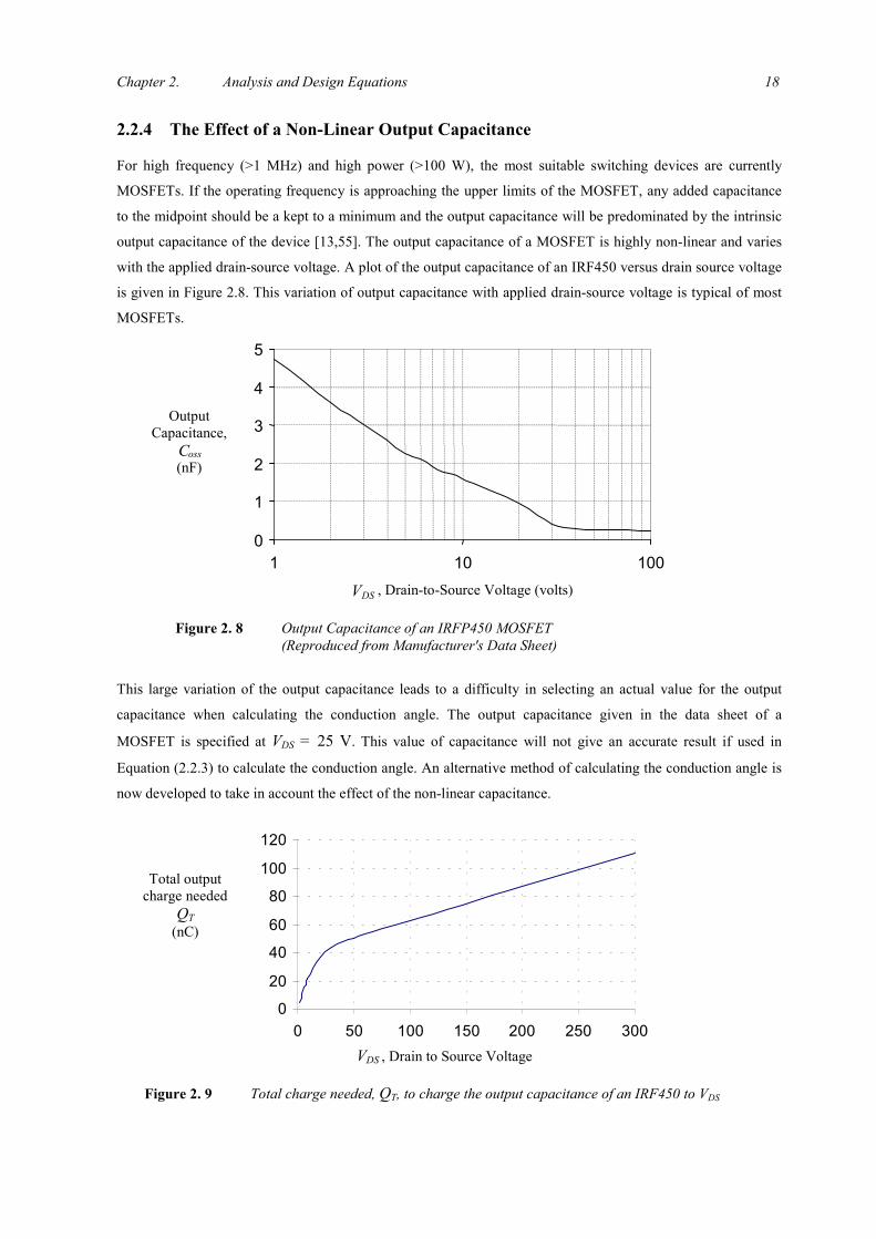
2.2.4 The Effect of a Non-Linear Output Capacitance
For high frequency (>1 MHz) and high power (>100 W), the most suitable switching devices are currently
MOSFETs. If the operating frequency is approaching the upper limits of the MOSFET, any added capacitance
to the midpoint should be a kept to a minimum and the output capacitance will be predominated by the intrinsic
output capacitance of the device [13,55]. The output capacitance of a MOSFET is highly non-linear and varies
with the applied drain-source voltage. A plot of the output capacitance of an IRF450 versus drain source voltage
is given in Figure 2.8. This variation of output capacitance with applied drain-source voltage is typical of most
MOSFETs.
This large variation of the output capacitance leads to a difficulty in selecting an actual value for the output
capacitance when calculating the conduction angle. The output capacitance given in the data sheet of a
MOSFET is specified at VDS = 25 V. This value of capacitance will not give an accurate result if used in
Equation (2.2.3) to calculate the conduction angle. An alternative method of calculating the conduction angle is
now developed to take in account the effect of the non-linear capacitance.
OutputCapacitance,
Coss(nF)
0
1
2
3
4
5
1 10 100
VDS , Drain-to-Source Voltage (volts)
Figure 2. 8 Output Capacitance of an IRFP450 MOSFET(Reproduced from Manufacturer's Data Sheet)
Total outputcharge needed
QT(nC)
0
20
40
60
80
100
120
0 50 100 150 200 250 300
Figure 2. 9 Total charge needed, QT, to charge the output capacitance of an IRF450 to VDS
VDS , Drain to Source Voltage
Chapter 2. Analysis and Design Equations 19
Figure 2.9 shows the total amount of charge needed, QT, to charge the output capacitance of an IRF450 to a
drain source voltage of VDS. The charge needed can either be measured experimentally (with the gate-source
shorted) or calculated using numerical integration of the output capacitance given in the data sheets [9]. Figure
2.9 is the result of such a numerical integration. The energy stored in the output capacitance is the area between
the y-axis and the charging curve of Figure 2.9.
This non-linear capacitance will affect the shape of the midpoint voltage as it swings from one rail to the other
during the dead-time, which will no longer be sinusoidal. To study the affect that this non-linear capacitance has
on the midpoint voltage, it will be assumed that the output capacitance is a loss-less non-linear capacitor with no
hysteresis i.e. the energy required to charge it equals the energy returned during discharging and the
charge/discharge curves are identical. It is also assumed that the load current is still sinusoidal and that the
inverter is operating in Class-DE mode. With these assumptions, the effect that this loss-less non-linear
capacitor has on the shape of the midpoint voltage can be calculated using numerical integration. The result of
such a numerical integration can be seen in Figure 2.10, which shows the voltage across the high side switch,
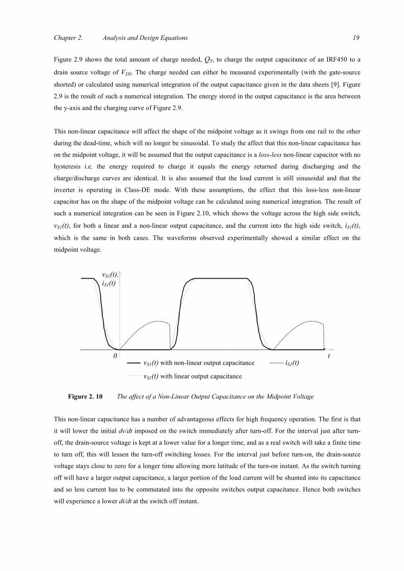
vS1(t), for both a linear and a non-linear output capacitance, and the current into the high side switch, iS1(t),which is the same in both cases. The waveforms observed experimentally showed a similar effect on the
midpoint voltage.
This non-linear capacitance has a number of advantageous effects for high frequency operation. The first is that
it will lower the initial dv/dt imposed on the switch immediately after turn-off. For the interval just after turn-
off, the drain-source voltage is kept at a lower value for a longer time, and as a real switch will take a finite time
to turn off, this will lessen the turn-off switching losses. For the interval just before turn-on, the drain-source
voltage stays close to zero for a longer time allowing more latitude of the turn-on instant. As the switch turning
off will have a larger output capacitance, a larger portion of the load current will be shunted into its capacitance
and so less current has to be commutated into the opposite switches output capacitance. Hence both switches
will experience a lower di/dt at the switch off instant.
Figure 2. 10 The affect of a Non-Linear Output Capacitance on the Midpoint Voltage
vS1(t) with non-linear output capacitance iS1(t)t
vS1(t),iS1(t)
0
vS1(t) with linear output capacitance

Chapter 2. Analysis and Design Equations 20
From Figure 2.9 we can see that a MOSFET will require a specific amount of charge, QT, to raise its drain-
source voltage to a given supply voltage, Vs. If the inverter is operating in Class-DE mode, then we can say the
charge removed from the midpoint by the load current must equal the total charge needed to raise one and lower
the other output capacitance of each MOSFET through a voltage of Vs. Thus, to calculate the conduction angle
needed for this supply voltage, we can equate the charge removed from the midpoint during the dead-time to
QT, giving
To QQ 22 =
Tsp QdttIs
s
2)sin( =∫ωπ
ωφω (2.2.33)
Solving the integral, we have
12
cos −=p
Ts
IQω
φ (2.2.34)
This equation has effectively replaced CoVs with the total charge needed to charge the output capacitance, QT,
and as QT is a measurable fixed quantity, it will give a more definitive result for the conduction angle required.
As QT is a non-linear function of Vs, the conduction angle required (given a constant load) will now vary as Vs
changes and the conduction angle calculated above will only be true for one value of the supply voltage.
A useful quantity to the designer, namely the effective output capacitance, Co-eff, of the MOSFET is now defined
as
s
Teffo V
QC =− (2.2.35)
This is the effective output capacitance of the MOSFET at only one particular supply voltage. However, if it is
calculated for its normal operating voltage level e.g. 80% of its maximum VDS, it will give the designer a good
measure of the MOSFET high-frequency characteristics. This value of output capacitance can be used in
simulations of the inverter, in power dissipation calculations and in equation (2.2.4) to calculate the maximum
operating frequency. It will also give the same result as equation (2.2.34) for the conduction angle if used in
equation (2.2.3).
If turn-on occurs at zero-load-current, then the power delivered can be calculated as before in equation (2.2.8)
by multiplying average current through each switch by the supply voltage, giving
( )φπ
cos12
−= psout
IVP (2.2.36)

Chapter 2. Analysis and Design Equations 21
Since this result is not dependent on the wave-shape of the midpoint voltage during the dead-time, this equation
will hold for non ZVS provided turn on occurs at zero-load-current. If the output capacitance is loss-less, the
real part of the load impedance may be calculated by equating power delivered to power dissipated, giving
( )2
cos12
2 RIIV pps =− φπ
(2.2.37)
Rearranging the above for R we have
( )φπ
cos1 −=p
s
IV
R (2.2.38)
This is the result obtained previously in equation (2.2.27) using the effective load impedance approach, however
this result shows that the value of R required is not dependent on the shape of the midpoint voltage during the
dead-time. The phase of the fundamental of the midpoint voltage with a non-linear capacitance will be similar to
that of the one with a linear capacitance. Thus, the inductance and capacitance required in the LCR network may
be found to a good degree of accuracy by using the conduction angle calculated in (2.2.34) in the equations
developed previously (2.2.27-2.2.31) using the effective load impedance approach.
2.2.5 Design Example
A summary of the design equations and procedure followed when designing a half-bridge Class-DE inverter is
given in Appendix D. A typical design procedure for a Class-DE inverter would start by selecting the desired
operating Voltage Vs and peak current Ip for a particular switching device. In this case, the switching devices
being used are two IRFP450 MOSFETS. These are 500 V, 14 A devices with an output capacitance of, Coss =
720 pF, specified at VDS = 25 V. The supply voltage of the inverter is selected to be Vs = 300 V, the peak current
through the device to be Ip = 16 A, and the desired operating frequency to be 5 MHz. The conduction angle
required at this supply voltage, operating current and frequency must now be calculated. If the specified output
capacitance, Coss, given in the data sheet as 720 pF, is used in equation (2.2.3), then
o
p
sos
IVC
9912
cos 1 =
−= − ω
φ
The above method produces an inaccurate value of φ because of the large variation of the output capacitance,
but is included here for comparison with the total charge method. The total charge needed to charge the output
capacitance to 300 V can be seen from Figure 2.9 to be 110 nC. Using QT = 110 nC in equation (2.2.34), we
have
o
p
Ts
IQ
12512
cos 1 =
−= − ω
φ
This is a more accurate result and thus this conduction angle will be used in the following calculations. The
power output of the inverter will be given by equation (2.2.8), thus

Chapter 2. Analysis and Design Equations 22
( ) kW202.1cos12
=−= φπ
psout
IVP
The phase lag, α , between the fundamental component of the midpoint voltage and the load current can be
found using equation (2.2.16), hence
o36sin
cossintan 21 =
+−= −
φφφφπα
The designer must now select the desired value of the Q of the resonant LCR network (usually about 3 to 5).
Selecting Q = 3.74 (this value is selected with prior knowledge of the actual practical value of the series
resonant capacitance used later in the text), the natural resonant frequency of the LCR network can then be
found using equation (2.2.30), giving
=
−+
=
QQf
f sr
αα tan4tan2
2
4.54 MHz
Using this value of fr, the value of the resistance, inductance and capacitance in the LCR network can be found
using equation (2.2.27) and the following expressions (where rr fπω 2= )
( )φπ
cos1 −=p
s
IV
R = 9.4 Ω
H1.23 µω
==r
RQLRQL
Crr ωω11
2 == = 1 nF
The Average current and RMS current through each switch can be using equation (2.2.22) and (2.2.23)
( )φπ
cos12
−=−p
avgS
II = 4 A
πφφ
2)2sin2(
2−
=−p
rmsS
II = 7.3 A
To summarize:
The total inductance of the LCR network must be 1.23 µH, the capacitance is 1 nF and the load resistance is
9.4 Ω. The resonant frequency of the LCR network will be 4.54 MHz. The peak current through the MOSFETs
is 16 A, the RMS current is 7.3A and the maximum voltage across them will be 300 V. The power output of the
inverter will be 1.2 kW at 5 MHz, and the switches will have to be operated at a conduction angle of 125 o (i.e.
a duty cycle of 35 %).
The theoretical analysis and design equations were confirmed by simulation on HB-Plus. The above design
example was simulated on HB-Plus [57] using ideal switches with an effective output capacitance of 367 pF
(calculated using equation (2.2.35)). The results can be seen in Appendix B and are in excellent agreement with
theoretical predictions.

Chapter 2. Analysis and Design Equations 23
2.6 Other Class-DE Topologies
The two other topology types capable of operating in Class-DE mode are the voltage-fed series resonant
full-bridge inverter and the voltage-fed series resonant push-pull inverter. The principle of the operation is
identical to that of a half-bridge. The design equations for these will require impedance transformations of the
equations developed for a half-bridge inverter. The various realizations of these two topologies are not
investigated here. One fact of concern in a push-pull inverter however, is that when a switch turns off, half the
current will be commutated into its output capacitance, but the other half must be instantaneously commutated
into the other leg of the transformer, to charge the other switch's output capacitance. Rapidly changing currents
in transformers will cause practical problems. In addition to Class-DE inverters, a family of Class-DE rectifiers
has also been introduced by Hamill [8,25]. This gives rise to the possibility of Class-DE2 DC/DC converters but
neither of these is discussed here.

24
CHAPTER 3. TOPOLOGY, SWITCHING DEVICES ANDSIMULATION
3.1 CHOICE OF THE TOPOLOGY
The three main realizations of a Class-DE inverter are in the form of a half-bridge inverter, full-bridge inverter
and a push-pull inverter. Push-Pull offers some advantages over the full-bridge or half-bridge form. The main
advantage of the push-pull form is that the drive signals (i.e. Gate drive signal) for both switches are referenced
to ground. Hence there is no level shifting required and an absence of all its associated practical problems. For
this reason the first attempt of implementing a Class-DE inverter was in the form of a 1 MHz, 500 W push-pull
inverter using a conventional transformer. However, there are some inherent limitations of a push-pull inverter
associated with its coupling transformer. Conventional transformers have a maximum frequency and power
limit. They also have inherent parasitic leakage inductances, coupling capacitances and winding capacitances.
These parasitics made the operational waveforms of the push-pull inverter extremely oscillatory and thus very
difficult to adjust the inverter to Class-DE operation. A better solution when implementing a push-pull topology
would be to use a hybrid-balun type transformer with the DC supply connected to the common center terminal.
This has a better high frequency response than a conventional transformer but will still have the limitations
mentioned above. High efficiency operation may possibly be attained with some tuning at a specific frequency
but some ringing will always be present. Thus using a push-pull topology it is difficult to obtain discernible
Class-DE operation in the HF band at power levels above a few hundred watts.
A half-bridge inverter has a major advantage over a push-pull topology in that it does not require a transformer
and hence does not have the inherent practical limitations associated with it. If the parasitic impedances due to
the inter-connections and the physical construction of the inverter can be reduced to an acceptably low
magnitude at the operating frequency, then a half-bridge inverter is almost certain to be perform as expected.
The actual operation of a half-bridge inverter can be deduced from the midpoint voltage and load current for
almost all load conditions. The inverter can be adjusted to Class-DE mode of operation by simply observing the
midpoint voltage. A half-bridge inverter is fundamentally a very broadband topology and its bandwidth can
potentially extend from DC to its highest designed operating frequency. However, the major disadvantage of a
half bridge inverter is that it has two independent switches, one of which is floating. Hence, in the MHz region,
there are considerable practical problems associated with physical construction of the half-bridge inverter and
layout difficulties caused by having two independent switches. Likewise, the control, timing and gate-drive of
two independent MOSFETs, one of which is floating, present some challenging technical problems in the MHz
region. However, the practical problems associated with a half-bridge inverter at high powers and high
frequencies (MHz region) are found in this thesis to be solvable to a satisfactory degree.
A full-bridge inverter has the same switch utilization factor as a half-bridge inverter. However it requires four
switches instead of two, which multiply the technical problems associated with the physical construction of the
inverter and time skew between the various drive signals. At MHz frequencies, a full-bridge inverter thus offers

Chapter 3. Topology, Switching Devices and Simulation 25
no advantages over a half-bridge inverter. It is therefore the author’s opinion that the most suitable topology for
a Class-DE inverter operating, in the HF band at power levels greater than a few hundred watts, is a voltage-fed
half-bridge series resonant inverter.
3.2 CHOICE OF THE SWITCHING DEVICE
An ideal switch should have no on-resistance, an infinite blocking voltage capability, no parasitic inductance or
capacitance and infinitesimal switching times. The switch should require minimal energy to change its state
from on to off or vice-versa. Solid-state transistors approximate an ideal switch to a good degree up to many
kHz. They have enabled power switch-mode type circuits to be widely implemented for many applications.
The principal requirement of a switching device used in a switch-mode type circuit is that it has fast enough
switching times for operation at the desired frequency. As a rough guide it should be capable of switching
completely on or off in less than 5% of the period. Presently, the solid-state power devices most suited for
switching operation in the MHz region, are switch-mode and RF MOSFETs [16]. MOSFETs have fast switching
times as they are majority carrier devices and hence their turn off time is not dependent on the recombination of
minority carriers. The most common and fastest power MOSFET is an n-channel enhancement type.
3.2.1 N-Channel Enhancement-Type MOSFET
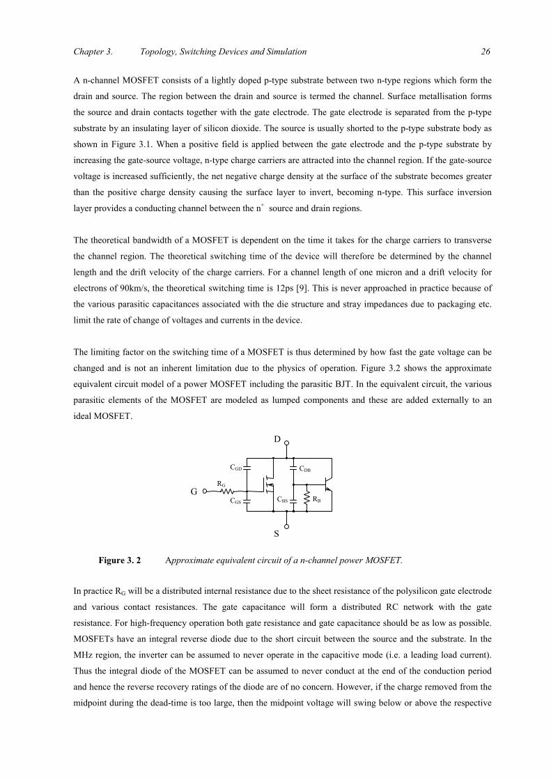
Figure 3.1 shows a cross section of a cell of planar vertical MOSFET
typically used in power MOSFETs. The power MOSFET is comprised of
many of these parallel-connected enhancement-mode MOSFET cells which
cover the surface of the silicon die.
Figure 3. 1 Structure of a vertical n-channel enhancement-type MOSFET
Source
Drain
Gate
Circuit Symbol
Gate
Drain
SourceSource
p (body)
n+
p (body)
ParasiticBJT
Gateoxide
SourceMetallisation
Currentpath
Gate
n+ n+ n+
n+n+
n- n-
Chapter 3. Topology, Switching Devices and Simulation 26
A n-channel MOSFET consists of a lightly doped p-type substrate between two n-type regions which form the
drain and source. The region between the drain and source is termed the channel. Surface metallisation forms
the source and drain contacts together with the gate electrode. The gate electrode is separated from the p-type
substrate by an insulating layer of silicon dioxide. The source is usually shorted to the p-type substrate body as
shown in Figure 3.1. When a positive field is applied between the gate electrode and the p-type substrate by
increasing the gate-source voltage, n-type charge carriers are attracted into the channel region. If the gate-source
voltage is increased sufficiently, the net negative charge density at the surface of the substrate becomes greater
than the positive charge density causing the surface layer to invert, becoming n-type. This surface inversion
layer provides a conducting channel between the n+ source and drain regions.
The theoretical bandwidth of a MOSFET is dependent on the time it takes for the charge carriers to transverse
the channel region. The theoretical switching time of the device will therefore be determined by the channel
length and the drift velocity of the charge carriers. For a channel length of one micron and a drift velocity for
electrons of 90km/s, the theoretical switching time is 12ps [9]. This is never approached in practice because of
the various parasitic capacitances associated with the die structure and stray impedances due to packaging etc.
limit the rate of change of voltages and currents in the device.
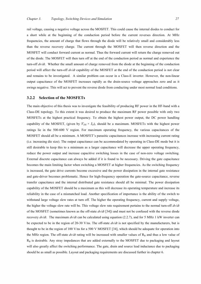
The limiting factor on the switching time of a MOSFET is thus determined by how fast the gate voltage can be
changed and is not an inherent limitation due to the physics of operation. Figure 3.2 shows the approximate
equivalent circuit model of a power MOSFET including the parasitic BJT. In the equivalent circuit, the various
parasitic elements of the MOSFET are modeled as lumped components and these are added externally to an
ideal MOSFET.
In practice RG will be a distributed internal resistance due to the sheet resistance of the polysilicon gate electrode
and various contact resistances. The gate capacitance will form a distributed RC network with the gate
resistance. For high-frequency operation both gate resistance and gate capacitance should be as low as possible.
MOSFETs have an integral reverse diode due to the short circuit between the source and the substrate. In the
MHz region, the inverter can be assumed to never operate in the capacitive mode (i.e. a leading load current).
Thus the integral diode of the MOSFET can be assumed to never conduct at the end of the conduction period
and hence the reverse recovery ratings of the diode are of no concern. However, if the charge removed from the
midpoint during the dead-time is too large, then the midpoint voltage will swing below or above the respective
S
D
GRB
CDBCGD
CGS
RG
CBS
Figure 3. 2 Approximate equivalent circuit of a n-channel power MOSFET.
Chapter 3. Topology, Switching Devices and Simulation 27
rail voltage, causing a negative voltage across the MOSFET. This could cause the internal diodes to conduct for
a short while at the beginning of the conduction period before the current reverses direction. At MHz
frequencies, the amount of charge that flows through the diode will be relatively small and considerably less
than the reverse recovery charge. The current through the MOSFET will then reverse direction and the
MOSFET will conduct forward current as normal. Thus the forward current will return the charge removed out
of the diode. The MOSFET will then turn off at the end of the conduction period as normal and experience the
turn-off dv/dt. Whether the small amount of charge removed from the diode at the beginning of the conduction
period will affect the turn-off dv/dt capability of the MOSFET at the end of the conduction period is not clear
and remains to be investigated. A similar problem can occur in a Class-E inverter. However, the non-linear
output capacitance of the MOSFET increases rapidly as the drain-source voltage approaches zero and as it
swings negative. This will act to prevent the reverse diode from conducting under most normal load conditions.
3.2.2 Selection of the MOSFETs
The main objective of this thesis was to investigate the feasibility of producing RF power in the HF-band with a
Class-DE topology. To this extent it was desired to produce the maximum RF power possible with only two
MOSFETs at the highest practical frequency. To obtain the highest power output, the DC power handling
capability of the MOSFET, (given by VDS × ID), should be a maximum. MOSFETs with the highest power
ratings lie in the 500-600 V region. For maximum operating frequency, the various capacitances of the
MOSFET should all be a minimum. A MOSFET’s parasitic capacitances increase with increasing current rating
(i.e. increasing die size). The output capacitance can be accommodated by operating in Class-DE mode but it is
still desirable to keep this to a minimum as a larger capacitance will decrease the upper operating frequency,
reduce the power output and increase capacitive switching losses in the case of non-zero voltage switching.
External discrete capacitance can always be added if it is found to be necessary. Driving the gate capacitance
becomes the main limiting factor when switching a MOSFET at higher frequencies. As the switching frequency
is increased, the gate drive currents become excessive and the power dissipation in the internal gate resistance
and gate-driver becomes problematic. Hence for high-frequency operation the gate-source capacitance, reverse
transfer capacitance and the internal distributed gate resistance should all be minimal. The power dissipation
capability of the MOSFET should be a maximum as this will decrease its operating temperature and increase its
reliability in the case of a mismatched load. Another specification of importance is the ability of the switch to
withstand large voltage slew rates at turn off. The higher the operating frequency, current and supply voltage,
the higher the voltage slew rate will be. This voltage slew rate requirement pertains to the normal turn-off dv/dt
of the MOSFET (sometimes known as the off-state dv/dt [34]) and must not be confused with the reverse diode
recovery dv/dt. The maximum dv/dt can be calculated using equation (2.2.7), and for 5 MHz 1 kW inverter can
be expected to be in the region of 20-30 V/ns. The off-state dv/dt is not specified by the manufacturers, but is
thought to be in the region of 100 V/ns for a 500 V MOSFET [34], which should be adequate for operation into
the MHz region. The off-state dv/dt rating will be increased with smaller values of RB and thus a low value of
RB is desirable. Any stray impedances that are added externally to the MOSFET due to packaging and layout
will also greatly affect the switching performance. The gate, drain and source lead inductance due to packaging
should be as small as possible. Layout and packaging requirements are discussed further in chapter 6.

Chapter 3. Topology, Switching Devices and Simulation 28
An optimum ratio of the above requirements must be selected. An IRFP450 MOSFET was found to have a good
balance between power rating, output capacitance and gate drive requirements. This is a 500 V, 14 A device
with a total gate charge of 150 nC, an output capacitance, Coss = 720 pF, and reverse transfer capacitance, Crss =
340 pF, with both capacitances specified for VDS = 25 V, VGS = 0 V and measured at 1 MHz. Hinchliffe et al
[19], showed that this MOSFET with an adequate gate driver and low inductance connections, is capable of
turning completely on or off in less than 10ns. This switching time was thought to be fast enough for operation
up to 5 MHz. This MOSFET was successfully used in a Class-E inverter operating up to 3.3 MHz, 450 W
[18,21]. It was decided to first operate the MOSFETs with a maximum DC supply voltage of 300 V and at a
peak current of 16 A. This would provide an adequate safety margin and allow the MOSFETs to run relatively
cool. An ideal Class-DE inverter operating at 5 MHz with a 300 V DC supply and 16A-peak current should
provide a theoretical output power of 1.2 kW as shown in section 2.2.5. A Spice simulation was then performed
of a half bridge inverter using two IRFP450 MOSFETs, operating at 5 MHz. The results of the simulation are
discussed in the following section.
The actual device used later to practically implement the inverter was the IRFP450LC. This has equivalent
power ratings of an IRFP450 but has lower device capacitances. This makes it considerably more suitable for
high frequency operation. The lower output capacitance means the gate drive requirements are reduced and a
smaller conduction angle will be required. Hence the power output will be higher. These facts enable the device
to operate at higher frequencies with a better efficiency.

Chapter 3. Topology, Switching Devices and Simulation 29
3.3 SIMULATION OF THE INVERTER
The objective of the simulating the inverter was to gain insight into its operation and determine the feasibility of
the inverter working up to 5 MHz using the IRFP450 MOSFETs selected in the previous section. The simulation
will give a more realistic picture of the actual operation of the inverter when using non-ideal switches. It also
enables the designer to learn what the effect of changing various parameters has on the operation of the inverter
and thus gain insight into the mechanics of its operation and observe the voltages and currents that will be
experienced in the circuit. The simulations were performed using PSpice.
3.3.1 Simulation of a Class-D Voltage-Fed Series Resonant Inverter
The first simulation attempted was of a classic Class-D half bridge inverter operating at 5 MHz with a 300V DC
supply, using two IRFP450 MOSFETs, and is included here to show the effect of capacitive switching losses.
The PSpice schematic circuit diagram used for the simulation of the Class-D inverter is given in Figure 3.3 and
the results of the simulation are given in Figure 3.4. The MOSFET model used in the simulation was simply the
IRF450 MOSFET model provided in the standard part libraries of the commercial version of PSpice.
+
150V
+
150V
C1
1nF
R-load11.9Ω
1.017uH
L1
+
-
V2
+V1 0.5
Rout-H
0.5
Rout-L
IRFP450
M2
IRFP450
M1
V
V
VPulse Sources - (V1 and V2) Tr, Tf =10ns ; PW = 70ns ; Period = 200ns
Figure 3.3 PSpice Schematic of the Class-D inverter
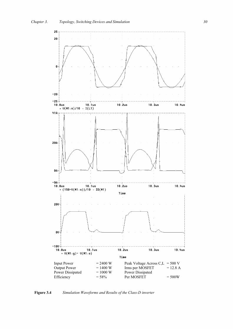
Chapter 3. Topology, Switching Devices and Simulation 30
Figure 3.4 Simulation Waveforms and Results of the Class-D inverter
Input Power = 2400 W Peak Voltage Across C,L = 500 VOutput Power = 1400 W Irms per MOSFET = 12.8 APower Dissipated = 1000 W Power DissipatedEfficiency = 58% Per MOSFET = 500W
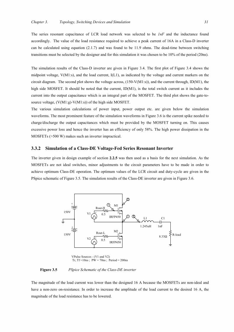
Chapter 3. Topology, Switching Devices and Simulation 31
The series resonant capacitance of LCR load network was selected to be 1nF and the inductance found
accordingly. The value of the load resistance required to achieve a peak current of 16A in a Class-D inverter
can be calculated using equation (2.1.7) and was found to be 11.9 ohms. The dead-time between switching
transitions must be selected by the designer and for this simulation it was chosen to be 10% of the period (20ns).
The simulation results of the Class-D inverter are given in Figure 3.4. The first plot of Figure 3.4 shows the
midpoint voltage, V(M1:s), and the load current, I(L1), as indicated by the voltage and current markers on the
circuit diagram. The second plot shows the voltage across, (150-V(M1:s)), and the current through, ID(M1), the
high side MOSFET. It should be noted that the current, ID(M1), is the total switch current as it includes the
current into the output capacitance which is an integral part of the MOSFET. The third plot shows the gate-to-
source voltage, (V(M1:g)-V(M1:s)) of the high side MOSFET.
The various simulation calculations of power input, power output etc. are given below the simulation
waveforms. The most prominent feature of the simulation waveforms in Figure 3.6 is the current spike needed to
charge/discharge the output capacitances which must be provided by the MOSFET turning on. This causes
excessive power loss and hence the inverter has an efficiency of only 58%. The high power dissipation in the
MOSFETs (>500 W) makes such an inverter impractical.
3.3.2 Simulation of a Class-DE Voltage-Fed Series Resonant Inverter
The inverter given in design example of section 2.2.5 was then used as a basis for the next simulation. As the
MOSFETs are not ideal switches, minor adjustments to the circuit parameters have to be made in order to
achieve optimum Class-DE operation. The optimum values of the LCR circuit and duty-cycle are given in the
PSpice schematic of Figure 3.5. The simulation results of the Class-DE inverter are given in Figure 3.6.
The magnitude of the load current was lower than the designed 16 A because the MOSFETs are non-ideal and
have a non-zero on-resistance. In order to increase the amplitude of the load current to the desired 16 A, the
magnitude of the load resistance has to be lowered.
Figure 3.5 PSpice Schematic of the Class-DE inverter
+
150V
+
150V
C1
1nF
R-load8.33Ω
1.245uH
L1
+
-
V2
+V1 0.5
Rout-H
0.5
Rout-L
IRFP450
M2
IRFP450
M1
V
V
VPulse Sources - (V1 and V2) Tr, Tf =10ns ; PW = 70ns ; Period = 200ns

Chapter 3. Topology, Switching Devices and Simulation 32
Figure 3.6 Simulation Waveforms and Results of the Class-DE Inverter
Input Power = 1150 W Peak Voltage Across C,L = 500V, 650VOutput Power = 1090 W Irms per MOSFET = 7.7 APower Dissipated = 60 W Power DissipatedEfficiency = 94.7% Per MOSFET = 30W

Chapter 3. Topology, Switching Devices and Simulation 33
To achieve the optimum Class-DE operation (i.e. zero-voltage and zero-load-current turn on), all that needs to
be adjusted is the phase lag of the load current and the pulse width of the gate drive signal. To increase the phase
lag of the load current, either a) the frequency can be increased making the load look more inductive, or b) the
inductance and/or the capacitance of the LCR network can be increased, thus increasing its inductive reactance.
In this simulation, the frequency is fixed at 5 MHz, and the inductance is varied to obtain the correct phase lag.
The optimum Class-DE operation was achieved by a succession of adjustments to the inductive reactance and
the duty-cycle of VPulse sources.
The three plots show the same voltages and currents as shown in the simulation waveforms of Figure 3.4 for a
Class-D inverter. Again it should be noted that the current, ID(M1), is the total switch current and consists of the
current through the MOSFETs conducting channel added to the current needed to charge/discharge its integral
output capacitance. As in Figure 3.4, the various simulation calculations of power input, power output etc. are
given below the simulation waveforms.
From the results of Figure 3.6, we can see that the MOSFETs now turn-on at almost zero voltage and zero-load-
current. The output power has decreased slightly to 1090 W, but the efficiency has dramatically increased to
94.7%. The power dissipation in the MOSFETs has decreased to a more practical value of only 30 W. Thus
from a power dissipation aspect, this inverter is practically more feasible. These simulation results also clearly
illustrate that by operating the inverter in Class-DE mode, the capacitive switching losses of a classic Class-D
inverter can be effectively eliminated. The simulation also shows that the PSpice model of the IRFP450
MOSFET is capable of operating at 5 MHz producing over 1 kW of power.
The PSpice simulation of the Class-DE inverter will predict a performance that is better than what can be
expected in practice as the simulation performed has the following limitations;
a) The PSpice model of the MOSFET is idealized and not entirely accurate,
b) No MOSFET dv/dt failure of any kind is modeled,
c) Thermal aspects, interference, ground loops and EMI are not considered,
d) Additional parasitics due to the physical layout of the circuit have not been included.
The additional parasitics can be included to a certain extent but the actual values have to be obtained empirically
off a fully constructed inverter or found approximately using calculations. This was considered not to be
worthwhile for these simulations. Even with the above shortcomings, the PSpice simulation will give a
reasonable evaluation of the how the inverter will perform, provided the MOSFETs are driven as required, and
the results were encouraging. It was felt that if the practical problems of implementing such an inverter can be
overcome, the inverter would have a good chance of working. As mentioned previously, the physical
implementation of the half-bridge inverter in the MHz region presents some challenging practical problems
associated with having two independent switches. These briefly are: the control, relative timing and gate-drive
of two independent MOSFETs, of which one is floating, and finally the layout and physical construction of the
inverter. These problems are dealt with in the following chapters.

34
CHAPTER 4. DRIVING THE INVERTER
The operation of a half bridge inverter requires the high and low-side switches to be alternately turned on and
off at the desired frequency and with the required duty-cycle. The switch state (i.e. on or off) is controlled by the
switch’s drive signal. In a Class-DE inverter the switches will be driven at exactly the same frequency and duty
cycle, but the drive signal for the high-side switch must be phase shifted exactly 180º degrees relative to the
low-side switch’s drive signal. The frequency and duty cycle required will depend on the values of LCR load
network and the output capacitance of the switches. The duty cycle will be between 0% and 50%.
A half-bridge inverter is fundamentally a very broadband topology and its bandwidth can potentially extend
from DC to its highest practically feasible operating frequency. In order to take advantage of this fact the
inverter driving circuitry must be capable of driving the half-bridge inverter over the widest range of frequencies
possible and with a variable duty cycle. If a means of varying the frequency and duty cycle of the inverter are
provided, then the only circuit changes that would be needed for different operating frequencies are the
inductance and capacitance of the tuned network. The inverter could then be tuned to Class-DE mode of
operation by simply adjusting the switching frequency and duty cycle of the inverter. This would enable very
quick modifications for different operating frequencies. The half-bridge inverter could then be used as a
broadband RF power supply.
The switches in a half-bridge inverter are controlled by the high and low-side switch drive signals. Therefore, in
order for the frequency and duty cycle of the inverter to be varied, a means of varying the frequency and duty
cycle of the switch drive signals over the widest range possible must be provided. Generation of these drive
signals is dealt with in the second section of this chapter. Operation of the inverter in a switching mode requires
the MOSFETs to be turned on and off by the drive signals. Turning the MOSFET on and off involves charging
and discharging the gate capacitance and this is dealt with in the next section.

Chapter4. Driving the Inverter 35
4.1 DRIVING THE MOSFET GATE
4.1.1 Requirements of the Gate-driver
In a switch-mode topology, the amount of time it takes for the switch to turn on or off is relatively important.
For reasonable performance in a Class-DE inverter, the switching devices should be capable of a switching in
less than approximately 5% of the period (for conduction angles is the region of 80º-150º). If the MOSFETs are
to switch in less than 5% of the period at 5 MHz, then their total time to switch on or off should be less than
10ns. Hence the MOSFET gate must be charged / discharged in less than 10ns.
The effective gate capacitance or input capacitance, Ciss, of MOSFET can be seen from Figure 3.2 to be
comprised of the gate-source capacitance and the gate-drain capacitance (or Miller capacitance) [31]. The total
gate charge, Qg, required to charge the gate of an IRFP450 MOSFET from 0 V to 12 V is 120 nC. This total
charge includes the (Miller) charge required to discharge the gate-drain capacitance when the MOSFET
switches from the off-state, with a VDS of 300 V, to the on state. If this entire charge is to be delivered in 10ns
then the gate-driver must supply an average current of Ig = 120nC/10ns = 12 A.
The loops around which the current will flow when charging and discharging the gate capacitance can be seen in
Figure 4.1. The current required to charge/discharge the gate capacitance must increase in a few nanoseconds
from zero to maximum of 12 Amps or more. If the rate of current rise is to be in the order of 4A/ns, then an
inductance of 1nH in the charging/discharging loop will cause a 4V voltage drop across it, reducing the drive
voltage available and slowing the rate of rise of the current [19,36]. It can be seen, therefore, that it is imperative
to keep the inductance of the gate charging and discharging loop to a minimum. The source-lead inductance is
part of the gate charging and discharging loop and in addition it has an induced voltage across it due the
changing drain current which further reduces the gate-drive voltage available. Thus the source-lead inductance
adversely effects the switching times and so it is desirable to keep it to an absolute minimum [19].
Gate-Driver
PowerMOSFET
+
G
D
S
ChargingLoop
DischargingLoop
Figure 4.1 Direct Drive of the MOSFET gate

Chapter4. Driving the Inverter 36
The gate-driver of Figure 4.1 can be considered to be a simple model of a commercial MOS-gate driver. If the
gate is to be charged and discharged through a resistive path, as shown in Figure 4.1, then all of the energy
supplied by the gate-driver will be dissipated in its internal resistances. The total power dissipated, Pd, in the
gate-driver circuitry will then be dependent upon the total gate charge, Qg, the gate-driver supply voltage, Vdri,
and the operating frequency, f. Hence
Pd = Qg Vdri f (4.1)
Calculating the power dissipated in a gate-driver, with a 12 V supply voltage, driving the gate of a IRFP450
MOSFET at 5 MHz, we have Pd = 110 nC × 12 V × 5 MHz = 7.2 W. Hence the gate-driver must be capable of
dissipating 7 W or more.
To summarize:
The MOSFET gate must be charged or discharged in less than 10ns, so the gate-driver must have rise and fall
times of less than 10ns. The gate-driver must source and sink in excess of 12A and should have as low an output
impedance as possible to prevent spurious turn on with high dVDS /dt. The gate-driver must be able to dissipate
in excess of 7 W. The charging and discharging loop must have the least inductance possible and its supply rails
should be very well decoupled.
4.1.2 Choice of the Method Used to Drive the MOSFET Gates
There are two practical choices for driving the gate capacitance with a square wave at a few MHz. The first uses
a gate-driver coupled to the gate through a transformer. The transformer is used to provide galvanic isolation
and the level shifting required for the high–side switch. The advantage of this system is that the high-side gate-
driver does not require a floating power supply as the power is coupled through the transformer. The
disadvantage is that transformers inherently have leakage inductances and coupling capacitances associated with
their construction. The leakage inductance of the windings makes it very difficult to obtain the rapid rise of
current required and will cause excessive ringing. The coupling capacitances limit the dv/dt and noise immunity
of the transformer. Transformer coupling also makes it complex to transfer DC information (i.e. duty ratio).
Improved operation can be obtained by using a large sinusoidal drive, as the transformer does not require the
high bandwidth needed for a square wave drive, and the leakage inductance of the transformer can be included
into a resonant circuit topology, El-Hamamsy [5]. In a resonant circuit topology, the energy stored in the gate
capacitance is resonated to an inductance and back again and hence much less power is dissipated than in a
hard-switched system. The disadvantages of a resonant circuit topology are that it is a single frequency system
and only a limited adjustment of the dead-time is possible. For the above reasons, a transformer-coupled gate
drive was considered not to be the best solution for this application.
The second way of driving the gate capacitance is to drive the gate directly with a gate-driver as shown in
Figure 4.1. This method will have the lowest loop inductances, provided the physical layout is designed
correctly, and thus will have the fastest charge and discharge times. If the MOSFET gate-drivers are provided

Chapter4. Driving the Inverter 37
with an independent power supply, they can then drive the MOSFET gates over the full bandwidth (DC-5
MHz), with any duty cycle. As fast switching times and a variable duty cycle are quintessential requirements of
a Class-DE inverter, this method was considered to be the best solution.
However this method has two practical problems, the first being that the high-side gate-driver must be provided
with a DC and RF isolated independent power supply. The high-side power supply's negative rail will
referenced to the source of the high-side MOSFET (the midpoint). The midpoint swings between ground and the
supply voltage at the operating RF frequency with slew rates of more than 30V/ns. The high-side power supply
should therefore have a minimum coupling capacitance from the point of connection at the high-side gate-driver
to ground, as this effectively appears as a capacitance added to the midpoint. The high-side power supply should
therefore appear as a very high impedance to ground at the operating RF frequency. The second problem of this
method is that the high-side gate-driver drive signal reference must be transferred or level-shifted from the
control circuitry’s reference, so that it is referenced to the midpoint. This problem is dealt with in the following
chapter.
4.1.3 The Gate-Driver
Incorporating the gate-driver directly onto the same die as the power MOSFET enables the lowest loop
inductances to be achieved and hence the fastest rise and fall times [9,36]. This solution was beyond the scope
and budget of this thesis and is left for future development. The next best solution is to mount the gate-driver
directly from the gate to the source and design the charging and discharging loop with the minimum leakage
inductance. This was the approach that was followed for this inverter.
For this application, the most feasible way to make the gate-driver, in terms of cost and development time, was
found to parallel four commercial MOS-gate drivers together. The most suitable commercial MOS-gate driver
was found to be the EL7104 in a DIP14 package from élantec. These have rise and fall times of 10ns with 1nF
load, can source and sink 4 A with 12 V supply voltage and have an output impedance of 3 ohms. Four of these
drivers paralleled will have a source and sink capability of 16 A and an output impedance of 0.75 ohms. The
power dissipation capability of the EL7104 is 1 W with the ambient at 25 ºC. Four of them in parallel will
therefore only have a power dissipation capability of 4 W, which is not high enough to dissipate the expected 7
W of power. However, the power dissipation capability was suitably increased by adding external heatsinking
with some air-cooling and this is discussed further in Chapter 6.
4.1.4 High and Low-side Gate-Driver Power supplies
The most common way of providing a floating power supply for the high-side is to use a bootstrap capacitor and
diode. The bootstrap diode in this inverter would have to withstand operation at 5 MHz, a blocking voltage
300 V, a forward current of more than 1 A and a recovery dv/dt of 30 V/ns. Operation at this frequency, voltage
and current would mean the reverse recovery losses of any commercial diode currently available would be
excessive. The reverse recovery current effectively adds more capacitance to the midpoint, which is undesirable.

Chapter4. Driving the Inverter 38
For these reasons a bootstrap supply is unsuitable for this inverter. A better solution was to use an independent
isolated power source. A 15 V, 1 A isolated DC-DC converter provided the floating power source and the DC
isolation needed for the high side. A common mode choke between the power supply and MOSFET gate-drivers
provided the RF isolation required. The common mode choke must be designed to minimize the coupling
capacitance across it. The low side power supply was provided by a non-isolated 15 V, 1 A DC-DC converter.
A 5 W, 8 Ω series resistance was included in both high and low-side 15 V power supply rails to limit the power
dissipation in the gate-drivers to a maximum of 7 W. Figure 4.2 shows the supply voltage, the power dissipated
and the current drawn by the gate-driver with an 8 Ω series resistance in the power supply rail.
4.1.5 Final Gate-Drive System
Figure 4.3 shows an overview of the final gate-driver and power supplies for the high and low-side. The
complete circuit can be found in Appendix C. High frequency layout techniques are imperative when designing
the circuit board and this is discussed further in Chapter 6. Figure 4.4 shows the gate to source voltage of the
high and low-side MOSFETs. The MOSFETs used are IRFP450LCs and waveforms were obtained with the
supply voltage at zero volts, hence the gate to source voltage of the high side MOSFET could be measured
directly. The main limitations of this system are the power dissipation, the leakage inductance, and the rise or
fall times can not be reduced much below 10ns. This system will not work much above 5 MHz. At higher
frequencies, new techniques such as those used by Leedham [36] and El-Hamamsy [5], will have to be
implemented to drive the gate capacitance. Driving the gate capacitance of high power MOSFETs will be one of
the main technical problems when implementing an inverter to work up higher frequencies such as 13.56 MHz
or 27 MHz.
Figure 4.2 Load-line of the Gate-Driver Power Supplies
0123456789
101112131415
0 0.1 0.2 0.3 0.4 0.5 0.6 0.7 0.8 0.9 1
Gate-Driver supply Current in Amps
Gate-Driversupplyvoltage, Vdri
Powerdissipated inGate-Driver,PD, in Watts
5 MHz operating point
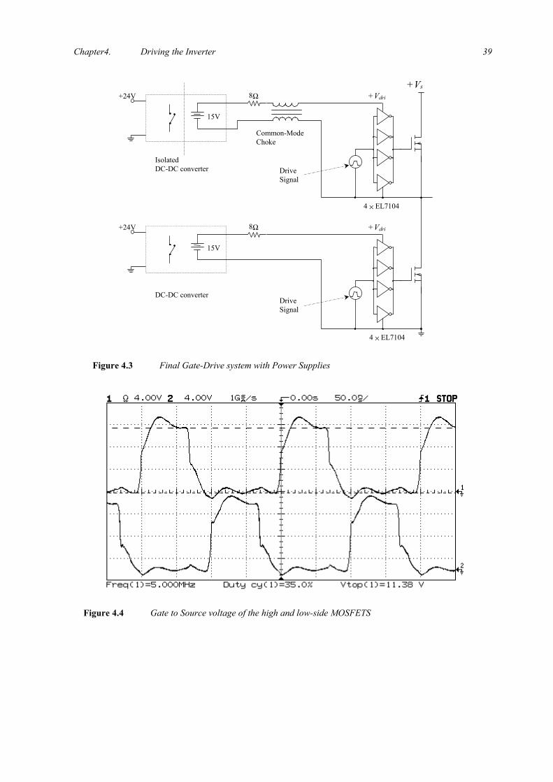
Chapter4. Driving the Inverter 39
Figure 4.3 Final Gate-Drive system with Power Supplies
IsolatedDC-DC converter
Common-ModeChoke
8Ω
8Ω
+Vs
4 × EL7104
4 × EL7104
+Vdri
+Vdri
15V
+24V
15V
+24V
DC-DC converter
DriveSignal
DriveSignal
Figure 4.4 Gate to Source voltage of the high and low-side MOSFETS

Chapter4. Driving the Inverter 40
4.1.6 MOSFET Gate Current when Operating in Class-DE Mode
If the inverter is operating in Class-DE mode then the entire gate charge will not have to be supplied all at once
in order to turn the MOSFET on or off. The Miller charge due to the gate to drain capacitance will be sourced
before the MOSFET is turned on and sunk after the MOSFET has turned off. This will lower the demand
placed on the gate-driver in one switching instant. These effects of Class-DE operation on the gate-drive
requirements can be seen in the waveforms of Figure 4.6. The voltage and current waveforms of Figure 4.6 are
marked on PSpice schematic of Figure 4.5. They are the current into the MOSFET gate, Ig(M1), the voltage
across the MOSFET, (150-V(M1:s))/10, and the gate to source voltage of the MOSFET, V(M1:g)-V(M1:s).
The periods during which the gate-drain capacitance is being charged and discharged is marked on Figure 4.6 as
the “Miller current”.
Figure 4.6 MOSFET Gate Current when operating in Class-DE mode
+
150V
+
150V
C1
1nF
R-load8.33Ω
1.245uH
L1
+
-
V2
+V1 0.5
Rout-H
0.5
Rout-L
IRFP450
M2
IRFP450
M1
V
V
VPulse Sources - (V1 and V2) = 12V Tr, Tf =10ns ; PW = 70ns ; Period = 200ns
Figure 4.5 PSpice Schematic of the Class-DE inverter

Chapter4. Driving the Inverter 41
The mechanism of operation may be described by the following sequence of events. After the low-side
MOSFET has turned off, the midpoint voltage will rise and the voltage across the high side switch will fall. The
gate voltage of the high-side MOSFET will still be low, but as the voltage across the MOSFET is falling the
high-side gate-driver must first source the current needed to discharge the gate-drain capacitance (Miller
current). Once the voltage across the MOSFET has stopped falling and reached zero, the current needed to
discharge the gate-drain capacitance will cease but the gate-driver must now source the current needed to charge
the gate of the MOSFET to 12V (Vdri) to turn it on. Similarly, when the MOSFET is turned off the gate
capacitance must be discharged from 12V(Vdri) to 0V first, turning the MOSFET off. The gate-driver must then
sink the current injected into the gate terminal by the gate-drain capacitance as the voltage across the MOSFET
rises (Miller current). The gate-driver must therefore have a low enough impedance to sink this current without
the gate voltage rising high enough to turn the MOSFET back on.

Chapter4. Driving the Inverter 42
4.2 DRIVE SIGNAL GENERATION
4.2.1 Requirements of the Drive-Signal-Generator
The first requirement of the drive-signal-generator is the ability two generate two drive signals of exactly the
same frequency and duty cycle but are always phase shifted exactly 180º degrees relative to each other. The
second requirement of the drive-signal-generator is the ability to vary the frequency and duty cycle of the drive
signals. The duty cycle (or dead-time) of both the high and low drive signals should be adjusted simultaneously
by a single adjustment method. This will ensure that both drive signals always have the same duty cycle. The
frequency range of the inverter was desired to be 50 kHz to 5 MHz. Resolution of the drive signals should be at
least 2% of period which at 5 MHz corresponds to rise and fall times of less than 4ns. The duty cycle should be
adjustable over the range 25%-48%. At 5 MHz this means the dead-time will range from 4ns to 50ns. Lower
frequencies will require longer dead-times, hence a dead-time range of 4 - 400ns was thought to be reasonable
for testing purposes.
4.2.2 Conceptual Circuit of the Drive-Signal-Generator
Any circuit used to generate the drive signals should incorporate a divide by two circuit on the clock signal to
obtain a 50% duty cycle (even symmetry of each half cycle). The path that the two drive signals take should also
be of similar length and incorporate the same gates to ensure that the time skew between the two drive signals is
minimized. The number of gates should also be kept to a minimum, as the delay variation of each gate will have
a cumulative effect on the total delay variation of each drive signal. The dead-time for both drive signals should
be generated by the same circuit to ensure that both signals have the same duty cycle. This will also enable the
duty cycle of both drive signals to be adjusted simultaneously. The conceptual circuit used to generate the
control circuit is given in Figure 4.7.
+5v
J
K
CLK
Q
QClock AND
AND
CLK
Rising Edge Triggered MonostablePulse-Width equal tothe required dead-time
High-Side Drive Signal
Low-Side Drive SignalRising Edge Triggered Flip-Flop
Figure 4.7 Conceptual Circuit of the Drive-Signal-Generator
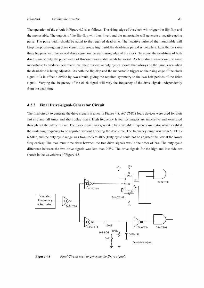
Chapter4. Driving the Inverter 43
The operation of the circuit in Figure 4.7 is as follows: The rising edge of the clock will trigger the flip-flop and
the monostable. The outputs of the flip-flop will then invert and the monostable will generate a negative-going
pulse. The pulse width should be equal to the required dead-time. The negative pulse of the monostable will
keep the positive-going drive signal from going high until the dead-time period is complete. Exactly the same
thing happens with the second drive signal on the next rising edge of the clock. To adjust the dead-time of both
drive signals, only the pulse width of this one monostable needs be varied. As both drive signals use the same
monostable to produce their dead-time, their respective duty cycles should then always be the same, even when
the dead-time is being adjusted. As both the flip-flop and the monostable trigger on the rising edge of the clock
signal it is in effect a divide by two circuit, giving the required symmetry to the two half periods of the drive
signal. Varying the frequency of the clock signal will vary the frequency of the drive signals independently
from the dead-time.
4.2.3 Final Drive-signal-Generator Circuit
The final circuit to generate the drive signals is given in Figure 4.8. AC CMOS logic devices were used for their
fast rise and fall times and short delay times. High frequency layout techniques are imperative and were used
through out the whole circuit. The clock signal was generated by a variable frequency oscillator which enabled
the switching frequency to be adjusted without affecting the dead-time. The frequency range was from 50 kHz -
6 MHz, and the duty cycle range was from 25% to 48% (Duty cycle could not be adjusted this low at the lower
frequencies). The maximum time skew between the two drive signals was in the order of 2ns. The duty cycle
difference between the two drive signals was less than 0.5%. The drive signals for the high and low-side are
shown in the waveforms of Figure 4.8.
74ACT14
74ACT14
74ACT14
CLRK
CLK
J QPRE
Q
74ACT109
74ACT14
74ACT08
74ACT08
D1N4148
150pF
10T-POT 500R
56R
+5v+5v
+5v
Dead-time adjust
VariableFrequencyOscillator
Figure 4.8 Final Circuit used to generate the Drive signals

Chapter4. Driving the Inverter 44
A limitation of this circuit is that it has a minimum duty cycle of 25%, which may be limiting at higher
frequencies. A second disadvantage of this circuit is that the dead-time is generated using an analog RC circuit.
This is sensitive to noise and can cause timing jitter. A better solution would be to use a digital generated
dead-time. A digital generated dead-time and a method of adjusting the duty cycle to less than 25%, are both
recommended for use at higher frequencies. The remaining problem of controlling the inverter is sending the
control information to the high side switch. This is the subject of the next chapter. The complete circuit of the
Drive-signal-generator is given in Appendix-C. A possible future circuit that solves the above problems is given
below.
4.2.4 Possible Future Circuit
Figure 4.9 Drive signals generated by the Drive-Signal-Generator Circuit
+5v
J
K
CLK
Q
QClock AND
AND
DigitalDelay =Dead-Time
High-Side Control Signal
Low-Side Control Signal+5v
J
K
CLK
Q
Q
Figure 4.10 Possible Future Circuit
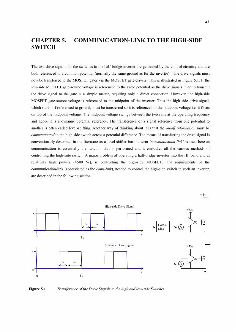
45
CHAPTER 5. COMMUNICATION-LINK TO THE HIGH-SIDESWITCH
The two drive signals for the switches in the half-bridge inverter are generated by the control circuitry and are
both referenced to a common potential (normally the same ground as for the inverter). The drive signals must
now be transferred to the MOSFET gates via the MOSFET gate-drivers. This is illustrated in Figure 5.1. If the
low-side MOSFET gate-source voltage is referenced to the same potential as the drive signals, then to transmit
the drive signal to the gate is a simple matter, requiring only a direct connection. However, the high-side
MOSFET gate-source voltage is referenced to the midpoint of the inverter. Thus the high side drive signal,
which starts off referenced to ground, must be transferred so it is referenced to the midpoint voltage i.e. it floats
on top of the midpoint voltage. The midpoint voltage swings between the two rails at the operating frequency
and hence it is a dynamic potential reference. The transference of a signal reference from one potential to
another is often called level-shifting. Another way of thinking about it is that the on/off information must be
communicated to the high side switch across a potential difference. The means of transferring the drive signal is
conventionally described in the literature as a level-shifter but the term ‘communication-link’ is used here as
communication is essentially the function that is performed and it embodies all the various methods of
controlling the high-side switch. A major problem of operating a half-bridge inverter into the HF band and at
relatively high powers (>500 W), is controlling the high-side MOSFET. The requirements of the
communication-link (abbreviated as the coms-link), needed to control the high-side switch in such an inverter,
are described in the following section.
Figure 5.1 Transference of the Drive Signals to the high and low-side Switches
Low-side Drive Signal
0
+
-
+
-
+Vs
+Vdri
+Vdri
High-side Drive Signal
To0
Coms-Link
td ton
To
td ton
5
5
t
t0
0

Chapter 5. Communication-link to the High-side Switch 46
5.1 REQUIREMENTS OF THE COMMUNICATION-LINK
In order to operate a half-bridge inverter in Class-DE mode, the timing of the switch turn on and off is relatively
important. For reasonably low noise, the resolution of the drive signal to the switch should be at least 2% of the
period. To obtain this resolution, the bandwidth of the communication-link will have to be at least twelve times
the required operating frequency. At 5MHz, the period is 200ns, hence the rise and fall times of the gate drive
signal should be at most 4ns. The bandwidth required of the communication-link to achieve these rise and fall
times will be 60MHz. The duty cycle of the drive signal will also be varying from approximately 10-50%. The
communication-link must therefore also be capable of transferring DC information. As the relative timing
between the two switches of the inverter is of fundamental importance to the operation of the inverter, the two
drive signals must be received without any time skewing, loss of information, or pulse width distortion relative
to the other sides drive signal.
When the high-side switch is on, the midpoint will be at the supply potential and the full supply voltage will be
applied across the communication-link and hence it must have an isolation voltage rated accordingly. Another
specification of importance is the dv/dt immunity of communication-link. During each switching transition, the
midpoint voltage swings from one rail to the other. This causes a high dv/dt at the midpoint and hence across the
communication-link. The higher the frequency, power and voltage, the higher dv/dt will be. The maximum dv/dt
expected in the inverter when operating at 5MHz,with a 300V supply voltage and a 1kW power output, is in the
region of 30V/ns. The communication-link must withstand these large voltage slew-rates without any false
triggering occurring. When operating a half-bridge inverter at high frequencies, it is desired that the output
capacitance from the midpoint to ground be kept to a minimum. The coupling capacitance across the
communication-link appears as a capacitance from the midpoint to ground and thus this should also be kept to a
minimum. In addition to the above conditions, the receiver side of the communication-link will be subjected to a
large amount of EMI caused by the rapidly changing voltages and currents of the power output stage. The
receiver should have a high immunity to this EMI and it should not cause any false triggering. In order for a half
bridge to be useful over a large range of frequencies and loads, the frequency and duty-cycle of the drive signals
should be variable over the largest range feasible. To this extent, the communication-link should not be the
limiting factor and should therefore be capable of transferring the drive signal over the specified frequency
range and for all the required duty-cycles.

Chapter 5. Communication-link to the High-side Switch 47
5.2 METHODS OF CONTROLLING THE HIGH-SIDE SWITCH
5.2.1 Pulse Transformer
The circuit given in Figure 5.2 uses a pulse-transformer to provide the galvanic isolation and
communication-link. The information is sent in a magnetic medium through the core of the transformer. A low
power pulse-transformer would be used to obtain a large bandwidth, followed by a current buffer. Transformers,
however, can not be built without inherent parasitic elements and will have a upper an lower frequency limit.
There is also always a trade off to be made between high frequency and low frequency response. To reduce the
rise and fall times, the primary and secondary windings should be tightly coupled. The tighter the coupling of
the windings, the higher the coupling capacitance between the primary and secondary will be. This coupling
capacitance will cause problems with a large dv/dt, inducing spurious signals into the windings. The capacitance
will also appear across the output of the inverter, which is undesirable. The leakage inductance of the windings
makes it difficult to obtain fast rise and fall times and will cause ringing. The windings of the transformer will
also act as pick up coils and are prone to EMI. Transformer coupling also makes it complex to transfer DC
information (i.e. duty ratios other than 50%). The close physical proximity of input and output restrict the layout
options the designer has when physically constructing the inverter. To summarize, with a square wave drive, it
will be difficult to obtain good signal fidelity using a transformer in a high power inverter operating in the HF
band.
Figure 5.2 Pulse-Transformer Isolation
+Vdri
+Vs
+Vdri
+Vs
Figure 5.3 Electronic Level-shifter
+Vdri
I

Chapter 5. Communication-link to the High-side Switch 48
5.2.2 Electronic Level-Shifters
An electronic level-shifter works on the principle of having a current source referenced to a fixed potential. The
reference potential is usually that of the low side switch’s source, hence they also called common source level-
shifters. The drive signal causes a certain current to be drawn through a current source regardless of the voltage
across it. The current is sensed by the receiving side and turned into on/off information. Electronic level-shifters
do not provide galvanic isolation. A simple common source non-inverting level-shifter is given in the Figure
5.3. The output capacitance and the power dissipated by the current source, limit the frequency and voltage it
can feasibly work at. A better solution, that decreases the amount of power dissipated, is to use a pulsed current
source, which is then latched on the receiving side. Current Pulsed circuits are based on the following two
topologies;
Dual Current Pulsed LatchThis topology employs two pulsed current sources. One pulsed current is used to set a flip-flop, which turns on
the switch, the other is used to reset the flip-flop, which turns off the switch. Many commercial half-bridge
drivers use this type of circuit. The problem with this circuit is that the reset current source has the full supply
voltage across it when it conducts the current pulse, causing power dissipation during each switching transition.
Hence the power dissipated by this topology increases with increasing frequency and becomes the limiting
factor at higher frequencies [9,24].
Single-Ended Current Pulsed LatchThe single-ended current pulsed latch was developed by Carter [9,24]. This circuit solves the problem of the
high power dissipation of the reset pulse by only having a single turn on current pulse. This pulse triggers a one
shot timer with a pulse width equal to Ton, followed by a delay that incorporates the dead time. The circuit is
relatively complex to implement and is most useful for fixed frequency power supplies of moderate power
levels (100W). It is not as useful in a high power RF generator as it is limited in its frequency range and dead
time adjustment.
The current source in all of the above circuits will have an output capacitance that appears across the
level-shifter. This capacitance limits the bandwidth and decreases the noise immunity of the level-shifter. The
dv/dt and isolation voltage is limited to the breakdown ratings of the current source transistor. Layout is difficult
because of the close proximity of the input to the output. The EMI immunity is low compared to optical
isolation.

Chapter 5. Communication-link to the High-side Switch 49
5.2.3 Opto-couplers
Logic to logic opto-couplers are in principle very simple to use. A logic input appears as a logic output on the
high side. They can transfer DC information and have static voltage isolation ratings of up to 5kV. They are
commercially available of up to 20Mbd, with rise and fall times of 10-20ns. This is not fast enough for this
application. Another problem of opto-couplers is that the propagation delay times change considerably with
temperature causing pulse width distortion and time skewing. The maximum dv/dt that opto-couplers are rated
for is in the region of 10V/ns which is below the required 30V/ns. The layout options are limited because of the
close proximity of the input to the output.
5.2.4 Fiber Optic Link
A basic fiber optic communication system is given in Figure 5.4. The LED is current driven by the drive signal.
The light emitted from the LED is sent down a length of fiber optic cable to the receiver. The receiver converts
the received optical signal into an analog output voltage. The receiver consists of a PIN photodiode and a
transimpedance amplifier. The output voltage of the amplifier is then level detected by a comparator and
converted into logic signal.
The galvanic isolation and dv/dt rating of this communication-link can be increased to almost any desired value
by simply lengthening the fiber optic cable. For a modest length of 10cm of fiber optic cable, the isolation
voltage is approximately 100kV. The dv/dt rating is difficult to calculate but as the coupling capacitance is
practically zero, even the highest realizable dv/dt will have little effect. The bandwidth available is an order of
magnitude higher than needed for this application, but the higher the bandwidth the higher the cost. The fiber
optic connection selected should have enough bandwidth to achieve the rise and fall times required. A fiber
optic link’s propagation delays are relatively constant over the working temperature range. Hence the pulse
width distortion and time skew are not degraded due to temperature variations. The only external electrically
conducting connections to the receiver side are the RF-isolated power supply connections. As the receiver-side
LED TransmitterPIN PhotodiodeReceiver
Comparator
+Vdri
+Vs
+5v+5v
Figure 5.4 Fiber Optic Communication-link

Chapter 5. Communication-link to the High-side Switch 50
circuitry is referenced to the midpoint, it can thus be totally enclosed by a screen connected to the midpoint,
offering excellent shielding from EMI. Electrical conductors are susceptible to electromagnetic fields and hence
will radiate and pick up EM noise. Fiber optic links neither emit nor receive EM noise and pass through noisy
environments unaffected. In addition to the above, when dealing with very rapidly changing currents, ground
noise can become a problem. A fiber optic link practically eliminates any ground loop or common mode noise
problems. To summarize, there are no fundamental limitations of a fiber optic system for this type of
application. It has more than enough bandwidth, dv/dt and voltage isolation capabilities and can transfer DC
information.
5.2.5 RF Modulated carrier signal
Another not well known method of communicating the on/off information is to use an RF modulated carrier
signal at a suitably high frequency, of say 100MHz. The carrier signal could be transferred across the isolation
barrier either magnetically (using, for example, a small poorly coupled transformer or a pair of loop antennas),
or electrically (using small picofarad or sub- picofarad capacitances). This method was not explored in detail by
the author but offers an interesting alternative method. Possible problems will be EMI susceptibility causing
spurious turn-on/off, and dv/dt immunity during the actual switching transitions.
5.2.6 Summary
Summary table
Usablefrequency
IsolationVoltage
Dv/dtCapability
DCInformation(Duty Ratio)
CouplingCapacitance
EMIimmunity
PulseTransformer
Limited to~10 MHz
~ low kV Limited Difficult Present Low
ElectronicLevel-shifters
~<14MHz ~<1000V Limited bycurrentsource
YesCout ofCurrentSource
Low
Opto-Couplers
<20Mbd <5kV <10v/ns Yes Very low Good
Fiber optics 1GHz+ As high asRequired
As high asRequired
Yes Negligible Excellent
From the above table it can be seen that a fiber optic link is the only communication-link that is guaranteed to
meet all the specifications needed for this application. A fiber optic link is relatively easy to implement and it
can be expected to perform to its specifications. It is the only communication-link that will work to the upper
end of the HF-band and is therefore the best method of controlling the high-side switch in a high power
RF-inverter. The following section deals with the development of a fiber optic communications link that is
suitable for a 5MHz, 1kW half-bridge inverter.

Chapter 5. Communication-link to the High-side Switch 51
5.3 IMPLEMENTATION OF A FIBER OPTIC COMMUNICATION-LINK
A primary requirement of the inverter is that there must be no time skew between the high and low-side drive
signals on reaching their respective switches. To solve this problem, identical fiber optic links were used to
transfer both the high and low-side drive signals. This enabled identical circuits to be used for both sides, so the
propagation delays of the drive signals would be the same, thus minimizing the time skew between them.
Similar circuits for both high and low-side also increases the modularity of the inverter. Having fiber optic links
to both sides means that the output stage can be galvanically isolated from all the control circuitry, which will
protect the control board in the case of catastrophic failure of the output stage. It also enables the control
circuitry to have a large physical separation from the power output stage and this creates many options for the
design of the layout. This large physical separation, in fact, allows an entire faraday cage to be constructed
between the control board and output power stage. This gives excellent isolation and shielding capabilities and
hence good EMI immunity. The physical separation possible with fiber optic links was found to be a major
advantage when designing and building a high frequency half bridge.
The fiber optic system selected was a 50Mbd link using cheap 1mm plastic fiber optic cable. The HFBR-1526
transmitter and HFBR-2526 receiver are used, and the fiber optic link has typical rise and fall times of 3.5ns.
The price of these components is relatively cheap for the bandwidth available, and so these were a cost-effective
solution. 1mm plastic fiber optic cable is readily available and easy to terminate. High frequency layout
techniques must be used throughout the transmitter and receiver circuits, to obtain the best performance.
5.3.1 LED Transmitter Drive Circuit
To obtain the best performance from the LED transmitter, it is preferable for the LED driver to employ
prebiasing and current peaking. To prebias the LED, it should be driven between a low and high current to
represent low and high logic levels respectively, and never completely turned off. The prebias current prevents
the junction and parasitic capacitances from discharging completely when the LED is in the “off” state, thus
reducing the amount of charge that the driver must transfer to turn the emitter back on. The simple inverter
circuit given in Figure 5.5 will provide a bi-level current drive to the LED. This circuit is used as the basis for
the LED driver circuit, and the calculations of the values of the drive resistors, RD and RB, are given the
following paragraph.
LED
RDRB
+5v+5v
Figure 5.5 Bi-Level Current Driver for the LED

Chapter 5. Communication-link to the High-side Switch 52
The most suitable high and low currents, IFon and IFoff, through the LED transmitter for the respective on and off
logic levels, must be chosen. From the data sheets of the LED, the forward voltage, VFon and VFoff, at the high
and low current levels respectively, can be obtained. For the circuit of Figure 5.5, two expressions can then be
written relating the LED current and their forward voltage to drive resistors. Equation 5.3.1 shows the
relationship of the high-level current, IFon, through the LED when the output of the inverter is high, to the drive
resistors. Equation 5.3.2 shows the relationship of the low-level current, IFoff, through the LED when the output
of the inverter is low, to the drive resistors.
B
Fon
D
FonFon R
VRV
I−
+−
=55
(5.3.1)
D
Foff
B
FoffFoff R
VRV
I −−
=5
(5.3.2)
A high current of 120mA and a low current of 2mA were selected as being suitable for the HFBR-1526 LED
transmitter. From the data sheets, VFon and VFoff for these two currents can be found. Equations 5.1 and 5.2 can
now be solved for RD and RB, hence RD was found to be 40Ω and RB to be 91Ω. The actual values of RD and RB
used are given in Figure 5.7. To practically implement this LED current driver, AC type CMOS inverters are
used as they have the fast rise and fall times required, can sink and source up to 24mA continuously, and have a
peak current rating of 75mA. The inverter of Figure 5.5 was implemented by paralleling four of the inverters
from a 74AC14 hex inverter to give the required current rating. When the LED driver circuit of Figure 5.5 is
used to drive the LED, slow rise and fall times are observed. This can be seen in Figure 5.6, where the upper
trace shows the LED forward voltage and the lower trace shows the output of the fiber optic receiver. The fiber
optic receiver output voltage varies between 1.8V and 2.8V giving a 1Vpp output voltage swing.
Figure 5.6 LED Forward Voltage and Fiber Optic Receiver Output Voltage

Chapter 5. Communication-link to the High-side Switch 53
The slow rise and fall times observed in Figure 5.6 occur because the parasitic and junction capacitances of the
LED have to charged and discharged. The rise and fall times can be improved considerably by using current
peaking. The addition of a simple RC speed-up network in parallel with the drive resistor, RD, of the circuit
given in Figure 5.5, was found to be highly effective. A series resistor-capacitor combination was found to be
preferable to just a plain capacitor, as this induced too much ringing. The optimum RC values were found
empirically and their values are given in the final LED driver circuit of Figure 5.7. The AC-CMOS inverters
have a peak source/sink current rating of 75mA each, and so they can easily provide the peak currents required.
The waveforms obtained with the final LED driver circuit of Figure 5.7 can be seen in Figure 5.8. The circuit
was found to be simple to implement and effective, achieving the fast rise and fall times required. The upper
trace of Figure 5.8 shows the LED forward voltage and the lower trace shows the output of the fiber optic
receiver.
74AC14
LED
Rb 100R
Rd
39R
37R 330pF
+5v
Figure 5.7 Final LED Driver Circuit
Figure 5.8 LED Forward Voltage and Fiber Optic Receiver Output Voltage with RC speed-up network
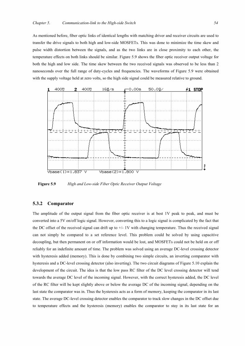
Chapter 5. Communication-link to the High-side Switch 54
As mentioned before, fiber optic links of identical lengths with matching driver and receiver circuits are used to
transfer the drive signals to both high and low-side MOSFETs. This was done to minimize the time skew and
pulse width distortion between the signals, and as the two links are in close proximity to each other, the
temperature effects on both links should be similar. Figure 5.9 shows the fiber optic receiver output voltage for
both the high and low side. The time skew between the two received signals was observed to be less than 2
nanoseconds over the full range of duty-cycles and frequencies. The waveforms of Figure 5.9 were obtained
with the supply voltage held at zero volts, so the high side signal could be measured relative to ground.
5.3.2 Comparator
The amplitude of the output signal from the fiber optic receiver is at best 1V peak to peak, and must be
converted into a 5V on/off logic signal. However, converting this to a logic signal is complicated by the fact that
the DC offset of the received signal can drift up to +/- 1V with changing temperature. Thus the received signal
can not simply be compared to a set reference level. This problem could be solved by using capacitive
decoupling, but then permanent on or off information would be lost, and MOSFETs could not be held on or off
reliably for an indefinite amount of time. The problem was solved using an average DC-level crossing detector
with hysteresis added (memory). This is done by combining two simple circuits, an inverting comparator with
hysteresis and a DC-level crossing detector (also inverting). The two circuit diagrams of Figure 5.10 explain the
development of the circuit. The idea is that the low pass RC filter of the DC level crossing detector will tend
towards the average DC level of the incoming signal. However, with the correct hysteresis added, the DC level
of the RC filter will be kept slightly above or below the average DC of the incoming signal, depending on the
last state the comparator was in. Thus the hysteresis acts as a form of memory, keeping the comparator in its last
state. The average DC-level crossing detector enables the comparator to track slow changes in the DC offset due
to temperature effects and the hysteresis (memory) enables the comparator to stay in its last state for an
Figure 5.9 High and Low-side Fiber Optic Receiver Output Voltage
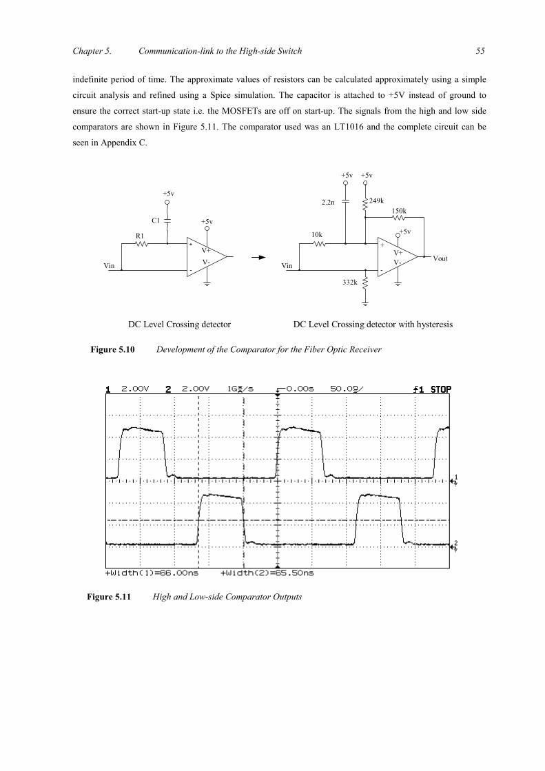
Chapter 5. Communication-link to the High-side Switch 55
indefinite period of time. The approximate values of resistors can be calculated approximately using a simple
circuit analysis and refined using a Spice simulation. The capacitor is attached to +5V instead of ground to
ensure the correct start-up state i.e. the MOSFETs are off on start-up. The signals from the high and low side
comparators are shown in Figure 5.11. The comparator used was an LT1016 and the complete circuit can be
seen in Appendix C.
Figure 5.10 Development of the Comparator for the Fiber Optic Receiver
DC Level Crossing detector DC Level Crossing detector with hysteresis
+
-
V+V-
C1
R1 10k
2.2n
332k
150k249k
+
-
V+V-
+5v +5v
+5v
+5v+5v
VoutVin Vin
Figure 5.11 High and Low-side Comparator Outputs

Chapter 5. Communication-link to the High-side Switch 56
5.4 CONCLUSIONS
This Fiber optic link was tested on a half bridge operating up to 1kW at 5MHz, with slew rates of up to 30V/ns.
From the midpoint voltage of the half bridge, it could be ascertained that the MOSFETs were switching at the
correct instants. The drive signal information must therefore have been transferred to the high and low side
switches correctly, and it can be concluded that the fiber optic link is functioning as required. The Fiber optic
communication-link proved to be a comprehensive solution that was relatively easy to implement has excellent
EMI and dv/dt immunity. Its high bandwidth enabled reliable operation from DC up to 5MHz, with almost any
duty cycle possible. To summarize, the fiber optic communication-link enabled a broadband, versatile and
adaptable half-bridge inverter to be built.
5.5 DISCUSSION
A type of idealistic half bridge inverter would have two light activated switches, which require minimal input
power and have infinitesimal switching times. To operate the inverter one would then simply direct light into the
desired switch to turn it on. By using a fiber optic cable with a receiver, comparator and current buffer, we are in
effect emulating such an ideal switch. The use of Fiber optic links in high power, high frequency inverters to
control floating devices has not been fully explored and its advantages have not been fully realized. The cost and
complexity of fiber optic links may have limited their use in the past but simple logic to logic fiber optic links
using cheap plastic fiber are now available.
The fiber optic communication-link described in this chapter was used to drive n-channel MOSFETs. This is a
switch with its on/off signal referenced to its cathode. A switching device may have its on/off signal referenced
to either its cathode or anode. A fiber optic communication-link can easily be adapted for use on both these
types of switches. Using Fiber optic connections to both high low side switches enables any combination of the
above switches to be used. Another possible application of fiber optic communication-link is to drive power
devices that have been stacked in series to increase their voltage rating. This would enable simultaneous
switching of the power devices, which are all at different potentials. In microprocessor controlled converters
where a communications link is required between the micro-board and the output stage, a fiber optic link could
perform the communication and level shifting in one step.
A fiber optic communication-link should be an excellent solution in any demanding power electronic
applications where frequency, voltage, dv/dt or EMI requirements preclude the use of more conventional
methods. A fiber optic link will also improve greatly improve the ruggedness of less demanding applications
and a 1mm plastic fiber link will provide a relatively inexpensive system.

57
CHAPTER 6. PHYSICAL CONSTRUCTION OF THEINVERTER
6.1 DESIGN CONSIDERATIONS OF THE INVERTER CONSTRUCTION
In order to obtain reliable operation of a Class-DE series resonant inverter and have clean waveforms, it is
critical that the half-bridge inverter output stage be constructed correctly. The first consideration is that the
decoupling-capacitor — inverter loop shown in Figure 6.1, must be designed to have the absolutely minimum
inductance feasible. This low inductance loop is needed because at the instant of turn off, the current is
commutated from one switch-leg to the other switch-leg (into its output capacitance). Also, the high-side switch
requires a low RF impedance through the decoupling-capacitor to ground when it turns on. The decoupling
capacitance should be large enough for operation at the lowest frequency and have the minimum ESR and ESL
possible.
The impedance of the decoupling-capacitor — inverter loop shown above in Figure 6.1 will increase linearly
with frequency. Thus it becomes more critical as the frequency increases to minimize its inductance in order to
obtain correct operation. As a rough guide, the impedance associated with the loop inductance should be at most
1/10 of the load impedance level the inverter is operating with. The load impedance of the inverter in this thesis
is in the region of 10 Ω and the operating frequency is 5 MHz. The loop should therefore have a maximum
impedance of 1 Ω, which at 5 MHz means the loop inductance must be less than 30 nH. If additional output
capacitance is added to the switches, it should be connected directly across the switch terminals with minimal
lead inductance. This will allow the current to easily commutate from the switch into its output capacitance. If
the midpoint voltage measurement is to be made referenced to ground, then a very good RF ground plane should
be provided for the low side switch. This will avoid ground loops and hence ground noise.
A second design consideration is that the stray capacitance added to the midpoint due to the physical
construction of the inverter should be kept to a minimum. Lower midpoint capacitance means that there will be
less power dissipation in the case of non-zero voltage switching, and that the conduction angle will not have to
+Vs
Power SupplyDecouplingCapacitors
Half-Bridge Inverter
Decoupling-Capacitor— Inverter Loop
Minimum InductanceConnections
Figure 6.1 The Decoupling-Capacitor — Inverter Loop

Chapter 6. Construction of the Inverter 58
be reduced so much, thus giving more output power. The high-side gate driver circuitry is referenced to the
midpoint, and so for RF purposes, all the high-side gate-driver circuitry may be considered to be an extension of
the midpoint. Hence, stray capacitance arising between the gate driver and its surroundings will add capacitance
to the midpoint and must be kept to a minimum. All the stray capacitances that arise from the construction of the
inverter and that add capacitance to the midpoint, are shown in Figure 6.2. The amount of added capacitance the
inverter can tolerate depends on the operating frequency, the load impedance level, the output power, the
inherent device output capacitance and the amount the conduction angle can be reduced.
The inverter designed in this thesis (given in section 2.2.5) has a conduction angle of 125º, and the MOSFETs
have an effective output capacitance of 367 pF. The total effective midpoint capacitance due to the MOSFETs
alone is therefore 734 pF. An addition of 100 pF to the midpoint due to the physical construction would increase
the total effective midpoint capacitance to 834 pF. This means the conduction will have to be reduced from 125º
to 115º, and the power output will be reduced from 1.2 kW to 1.1 kW. This reduction was decided to be an
acceptable amount and hence the addition of up to 100 pF of stray capacitance was tolerable.
A third design consideration of the half-bridge inverter is that the power MOSFETs must be provided with a
adequate means of thermal dissipation. The lower the thermal resistance provided to the MOSFETs, the cooler
they will run and hence the lower the on-resistance will be, increasing the system efficiency. Cooler MOSFETs
will also have a higher breakdown voltage and an increased load mismatch tolerance, hence their reliability and
lifetime will be extended. A final consideration, as described in Chapter 4, is that the inductance of the gate
charging and discharging loop through the gate-driver, must be designed to be of minimum value. The output
stage of the gate-driver must also be provided with a adequate means of thermal dissipation. Thermal dissipation
from the power output devices should also not adversely affect the gate-driver circuitry. Thermal isolation of the
gate driver circuitry from power output stage will alleviate this problem.
+Vs
Gate-driver Circuitry
Gate-driver Circuitry
Coms-Link
Stray CapacitanceTo be minimized
Figure 6.2 Stray Capacitances effectively adding to the Midpoint Capacitance

Chapter 6. Construction of the Inverter 59
6.2 ACTUAL CONSTRUCTION OF THE INVERTER
The IRFP450 MOSFETs used in this inverter are packaged in the industry standard TO-247AC case. This has a
drain lead inductance of 5 nH between the center of the die contact and the point on the drain lead 6mm from
the edge of the package. Similarly, it has a source lead inductance of 13 nH between the center of the die contact
and the point on the source lead 6mm from the edge of the package. The back-tab of the package is bonded
directly to the MOSFET die. The drain lead inductance can be practically eliminated by mounting each
MOSFET directly onto its own aluminum heatsink and using the heatsink as the drain connection to the
back-tab of the package. This required two isolated heatsinks, one of which would have the high-side MOSFET
mounted on it and hence is at the supply potential, and the other would have the low-side MOSFET mounted on
it and hence is at the midpoint potential. The midpoint heatsink was mounted so that it had enough physical
separation from the surrounding ground enclosure to minimize the stray capacitance to an acceptable level. The
separation of the two heatsinks from each other was optimized to obtain a compromise between added stray
capacitance and connection inductances. The layout of the heatsinks can be seen in Figure 6.3.
Low inductance connections must then be made from the source of the high-side MOSFET to the low-side
MOSFETs heatsink, from the source of the low-side MOSFET to ground, and from ground through the
decoupling power supply capacitors back to the high-side MOSFETs heatsink. These low inductance
connections were achieved by mounting the two heatsinks in the same plane, enabling a PCB to be placed
directly over the top of both heatsinks. This PCB is referred to as the main PCB board. The MOSFETs were
mounted through the main PCB board onto the heatsinks. The topside of the main PCB board was then used to
Figure 6.3 Front View of Inverter Output Stage Showing the Isolation of the Heatsinks

Chapter 6. Construction of the Inverter 60
provide the connections between the two heatsinks and to the gates of both MOSFETs. The center drain lead of
the MOSFET was removed in order to allow wider gate and source tracks. The entire topside of the main PCB
above the high-side heatsink was made a ground plane. This provided the low inductance connection from the
ground plane, through the decoupling power supply capacitors and to the drain of the high-side MOSFET. The
bottom side of the PCB was therefore connected directly to the heatsink and the decoupling capacitors were
connected between the topside and bottom side of the PCB. The decoupling power supply capacitors were
provided by twenty 68 nF, 500 V multi-layer ceramic capacitors paralleled with larger polypropylene capacitors.
Multi-layer surface mount ceramic capacitors have very low ESR and ESL and are imperative for this
application. The topside of the PCB over the midpoint heatsink was directly connected with plated feed-thru
holes to the bottom side. The topside of the PCB was extended to make the connection to the source of the high
side MOSFET. These connections can be seen in Figure 6.4, which shows the topside of the main PCB board.
The added stray capacitance to the midpoint due to the physical construction of this inverter was measured to be
90 pF. The inductance of decoupling-capacitor inverter loop is difficult to measure but is thought to be mainly
comprised of the two source lead inductances, hence it will be in the region of 26 nH.
The gate-driver circuitry was mounted on a separate PCB referred to as the Gate-driver board. The two boards
for the high and low side were mirror images of each other. These boards were mounted perpendicular to the
main PCB board. This enabled the gate-driver to be physically close to the MOSFET without breaking up the
low inductance connections to the sources of both MOSFETs. It also enabled low inductance gate charging and
discharging loops to be made. Mounting the gate driver boards vertically means there will be a free air-flow
over the boards, improving their thermal dissipation capabilities. The gate-driver boards will also be thermally
isolated from the power MOSFETs. The gate-driver boards and the fiber optic connections can be seen in
Figure 6.5.
Figure 6.4 Top View of Main PCB Board Showing the Layout of the Power MOSFETs

Chapter 6. Construction of the Inverter 61
The whole output inverter stage has a large physical separation to the drive signal generator board and all other
auxiliary circuit boards. This was made possible by use of fiber optic links to transfer both drive signals. All
other auxiliary circuit boards should be made with good RF construction techniques and with a good ground
plane as the inverter will generate a fair amount of RFI and EMI. It may prove necessary to provide additional
shielding for the auxiliary circuit boards but this was not needed in this inverter.
The inverter construction described above is approaching its operational limit at 5 MHz. For operation at higher
frequencies it will be necessary to employ a more suitable means of construction. A better solution would be to
construct the entire half-bridge on a ceramic substrate. This method will enable lower loop inductance, less
added stray capacitance and good power dissipation. With this technology, it should be possible to construct an
inverter that has the potential to operate to higher frequencies such as 13.56 MHz, and possibly 27 MHz.
Figure 6.5 Front View of Inverter Output Stage Showing the Gate-driver boards and Fiber Optic Links
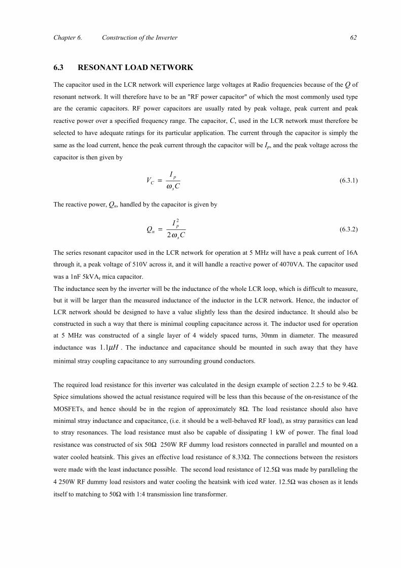
Chapter 6. Construction of the Inverter 62
6.3 RESONANT LOAD NETWORK
The capacitor used in the LCR network will experience large voltages at Radio frequencies because of the Q of
resonant network. It will therefore have to be an "RF power capacitor" of which the most commonly used type
are the ceramic capacitors. RF power capacitors are usually rated by peak voltage, peak current and peak
reactive power over a specified frequency range. The capacitor, C, used in the LCR network must therefore be
selected to have adequate ratings for its particular application. The current through the capacitor is simply the
same as the load current, hence the peak current through the capacitor will be Ip, and the peak voltage across the
capacitor is then given by
CI
Vs
pC ω
= (6.3.1)
The reactive power, Qn, handled by the capacitor is given by
CI
Qs
pn ω2
2
= (6.3.2)
The series resonant capacitor used in the LCR network for operation at 5 MHz will have a peak current of 16A
through it, a peak voltage of 510V across it, and it will handle a reactive power of 4070VA. The capacitor used
was a 1nF 5kVAr mica capacitor.
The inductance seen by the inverter will be the inductance of the whole LCR loop, which is difficult to measure,
but it will be larger than the measured inductance of the inductor in the LCR network. Hence, the inductor of
LCR network should be designed to have a value slightly less than the desired inductance. It should also be
constructed in such a way that there is minimal coupling capacitance across it. The inductor used for operation
at 5 MHz was constructed of a single layer of 4 widely spaced turns, 30mm in diameter. The measured
inductance was Hµ1.1 . The inductance and capacitance should be mounted in such away that they have
minimal stray coupling capacitance to any surrounding ground conductors.
The required load resistance for this inverter was calculated in the design example of section 2.2.5 to be 9.4Ω.
Spice simulations showed the actual resistance required will be less than this because of the on-resistance of the
MOSFETs, and hence should be in the region of approximately 8Ω. The load resistance should also have
minimal stray inductance and capacitance, (i.e. it should be a well-behaved RF load), as stray parasitics can lead
to stray resonances. The load resistance must also be capable of dissipating 1 kW of power. The final load
resistance was constructed of six 50Ω 250W RF dummy load resistors connected in parallel and mounted on a
water cooled heatsink. This gives an effective load resistance of 8.33Ω. The connections between the resistors
were made with the least inductance possible. The second load resistance of 12.5Ω was made by paralleling the
4 250W RF dummy load resistors and water cooling the heatsink with iced water. 12.5Ω was chosen as it lends
itself to matching to 50Ω with 1:4 transmission line transformer.
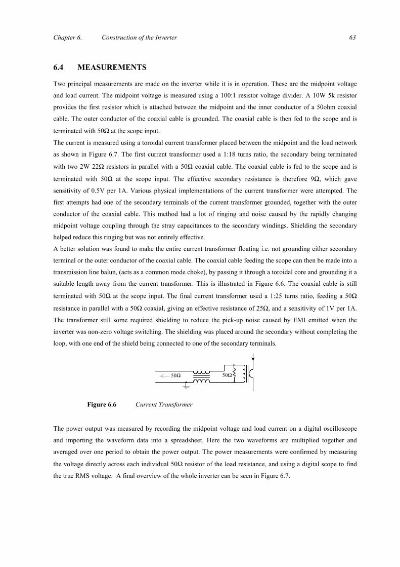
Chapter 6. Construction of the Inverter 63
6.4 MEASUREMENTS
Two principal measurements are made on the inverter while it is in operation. These are the midpoint voltage
and load current. The midpoint voltage is measured using a 100:1 resistor voltage divider. A 10W 5k resistor
provides the first resistor which is attached between the midpoint and the inner conductor of a 50ohm coaxial
cable. The outer conductor of the coaxial cable is grounded. The coaxial cable is then fed to the scope and is
terminated with 50Ω at the scope input.
The current is measured using a toroidal current transformer placed between the midpoint and the load network
as shown in Figure 6.7. The first current transformer used a 1:18 turns ratio, the secondary being terminated
with two 2W 22Ω resistors in parallel with a 50Ω coaxial cable. The coaxial cable is fed to the scope and is
terminated with 50Ω at the scope input. The effective secondary resistance is therefore 9Ω, which gave
sensitivity of 0.5V per 1A. Various physical implementations of the current transformer were attempted. The
first attempts had one of the secondary terminals of the current transformer grounded, together with the outer
conductor of the coaxial cable. This method had a lot of ringing and noise caused by the rapidly changing
midpoint voltage coupling through the stray capacitances to the secondary windings. Shielding the secondary
helped reduce this ringing but was not entirely effective.
A better solution was found to make the entire current transformer floating i.e. not grounding either secondary
terminal or the outer conductor of the coaxial cable. The coaxial cable feeding the scope can then be made into a
transmission line balun, (acts as a common mode choke), by passing it through a toroidal core and grounding it a
suitable length away from the current transformer. This is illustrated in Figure 6.6. The coaxial cable is still
terminated with 50Ω at the scope input. The final current transformer used a 1:25 turns ratio, feeding a 50Ω
resistance in parallel with a 50Ω coaxial, giving an effective resistance of 25Ω, and a sensitivity of 1V per 1A.
The transformer still some required shielding to reduce the pick-up noise caused by EMI emitted when the
inverter was non-zero voltage switching. The shielding was placed around the secondary without completing the
loop, with one end of the shield being connected to one of the secondary terminals.
The power output was measured by recording the midpoint voltage and load current on a digital oscilloscope
and importing the waveform data into a spreadsheet. Here the two waveforms are multiplied together and
averaged over one period to obtain the power output. The power measurements were confirmed by measuring
the voltage directly across each individual 50Ω resistor of the load resistance, and using a digital scope to find
the true RMS voltage. A final overview of the whole inverter can be seen in Figure 6.7.
50Ω 50Ω
Figure 6.6 Current Transformer

Chapter 6. Construction of the Inverter 64
Figure 6.7 Overview of theWhole Inverter
65
CHAPTER 7. EXPERIMENTAL RESULTS
The broadband design of the control circuitry, communication-link and gate-drive enabled the half-bridge output
stage to be driven from 50 kHz through to 6 MHz. The only circuit changes needed for the different operating
frequencies are the inductance and capacitance of the tuned network. The calculation of the values of the
inductance and capacitance for tuned LC network is simple and fast. The tuning procedure for Class-DE mode
of operation is relatively simple and can be done without any circuit changes. This enabled very quick
modifications for different operating frequencies. When operated in the Class-DE mode, the inverter was found
to be capable of delivering a power output of over 1 kW from 50 kHz to 5 MHz with an efficiency of over 90%.
The inverter used IRFP450LC MOSFETs, as these have a lower input, reverse transfer and output capacitance.
This lower output capacitance means the switches can be operated with a larger conduction angle for a given
frequency, and hence will output more power. Thus, at a operating frequency of 5 MHz, a supply voltage of
300 V and with load resistance of 8.33 ohms, the inverter can be expected to output slightly more power than
shown in the simulation of Section 3.3.3, which used IRF450 MOSFETs. The lower gate charge required for
the IRF450LC also lowered the power dissipated in the gate-drivers and allowed for a higher gate-drive voltage.
Tests on the inverter started at a low frequency and power and both were systematically increased. The inverter
could be operated in normal Class-D operation up to approximately 1 MHz. Up to this frequency, the inverter
operation was as good as could be expected using non-ideal switches and little problems were experienced.
Above 1 MHz, the inverter should be operated in such a way that the capacitive switching losses are reduced.
Above 3 MHz and at power levels greater than 500 W, the inverter must be operated as close as possible to true
Class-DE type of operation. When the inverter was operated in a non-zero voltage-switching mode, (i.e. the
switches were turning on with a non-zero voltage across them), the ringing noise and EMI emitted were very
apparent. Operating the inverter in the Class-DE mode reduced the ringing noise and EMI to a level that was
barely noticeable.
When operating below 3 MHz in Class-DE mode, the only significant loss in the inverter was due to the
on-resistance of the MOSFETs. The efficiency of the inverter at full output power for all frequencies up to
3 MHz was therefore in the region of 94%. The results up to 3 MHz were close to perfect and do not give the
designer much practical information. The test results presented in this thesis are therefore from 3 MHz upwards.
Above 3 MHz, the efficiency begins to decrease which is thought to be due to a number of reasons. These are:
a) Some turn-off loss will occur due to non-instantaneous switching,
b) Higher RMS currents will be experienced because of the smaller conduction angle required,
c) Loss associated with the drift resistance of the MOSFET when charging/discharging the output capacitance
d) Some capacitive discharge loss will occur at turn-on.
Chapter 7. Experimental Results 66
7.1 TUNING PROCEDURE FOR CLASS-DE OPERATION
The process of obtaining Class-DE operation starts by making the inductance and capacitance of the LC tuned
network with values as close as possible to the calculated ones. The conduction angle of the switches should
then be set to a value smaller than what was calculated (i.e. a larger dead-time). The supply voltage to the
inverter should be set at a relatively low value, which in this case was 100 V. The approximately correct phase
lag of the load current to the midpoint voltage should then be obtained. This is done by increasing the driving
frequency of the inverter above the resonant frequency of the LCR network until the midpoint voltage is seen to
swing almost to the opposite rail after turn-off. This effect can only be observed if the dead-time is larger than
required. The dead-time must then be adjusted until the switches turn on at the instant where the voltage across
them is the lowest. This process can then be repeated with smaller adjustments until optimum Class-DE
operation is obtained. The inductance and/or the capacitance of the tuned network can now be appropriately
adjusted to increase or decrease the operating frequency. The process described above is then repeated until the
inverter operates in Class-DE mode at the desired frequency. As the supply voltage is increased above 100 V,
slightly less dead-time and phase lag are required to obtain optimum Class-DE operation due to the non-linear
output capacitance of the MOSFETs.
The following section (Figure 7.1 to Figure 7.4) shows four cases of oscilloscope waveforms obtained while
tuning the inverter for Class-DE operation. The supply voltage in all four cases is 100 V and the LCR tuned
network remains unchanged. The only parameters that are varied are the switching frequency of the inverter and
the conduction angle of the switches. The oscilloscope waveforms shown for each case are the midpoint voltage,
the load current and the gate-source voltage of the low-side MOSFET. The waveforms are captured on a
HP54615B 500 MHz digital oscilloscope. For each case, the first oscilloscope screen capture shows the
midpoint voltage on channel-1 and the load current on channel-2. The voltage and current scale are both 1:1.
The second oscilloscope screen capture shows the gate-source voltage of the low-side MOSFET. Both of the
screen captures are triggered on the midpoint voltage and hence they have the same time line. Relative timing
comparisons between the two screen captures can thus be performed. Figure 7.5 shows how the efficiency varies
over the tuning procedure.

Chapter 7. Experimental Results 67
From the oscilloscope waveforms of Figure 7.1, it can be seen that non-zero voltage switching is occurring. This
is because in the period between the switch off instant and the point where the load current reaches zero, the
midpoint voltage does not swing all the way across to the opposite rail. This means that not enough charge is
removed from the midpoint by the load current before it reverses direction. To increase the charge removed
from the midpoint, the phase lag of the load current to the midpoint voltage must be increased. This is achieved
by increasing the switching frequency of the inverter and the effect of this can be seen in the following
waveforms of Case 2, Figure 7.2.
Midpoint Voltage and Load current
Gate-Source Voltage of the Low-side MOSFET
Figure 7.1 Case 1. Too Little Phase Lag

Chapter 7. Experimental Results 68
From the oscilloscope waveform of the midpoint voltage in Figure 7.2, it can be seen that after the switch-off
instant the midpoint voltage swings almost all the way to the opposite rail before the load current reaches zero.
The opposing switch however does not turn on at this instant and so when the current reverses direction the
midpoint voltage starts to swing back towards its original rail. The opposing switch only turns on after the
midpoint voltage has swung almost half way back to original rail. This means that the phase lag of the load
current is correct but the conduction angle is too small (i.e. the dead-time is too large) and the switch is turning
on too late. To remedy this the conduction angle simply has to be increased and the effect of this can be seen in
the following waveforms of Case 3, Figure 7.3.
Midpoint Voltage and Load current
Gate-Source Voltage of the Low-side MOSFET
Figure 7.2 Case 2. Too Much Dead-Time

Chapter 7. Experimental Results 69
The oscilloscope waveforms of Figure 7.3, show optimum Class-DE operation. The midpoint voltage swings
almost all the way to the opposite rail before the load current reverse direction and the opposing switch turns on
at this instant. Thus the switches are turning on at zero-voltage and zero-load-current (zero dv/dt). This
considerably reduces the amount of ringing caused by the switching transitions and the EMI emitted. These
effects can be observed in the clean waveforms above as compared to the previous cases. If the conduction angle
is increased further still then the switches will turn on before the midpoint voltage has reached the opposite rail
(i.e. they will turn on too early). The effect of increasing the conduction angle too much can be seen in the
following waveforms of Case-4, Figure 7.4.
Midpoint Voltage and Load current
Gate-Source Voltage of the Low-side MOSFET
Figure 7.3 Case 3. Optimum Class-DE Operation

Chapter 7. Experimental Results 70
From the oscilloscope waveforms of Figure 7.4, it can be seen that the switches are turning on before the
midpoint voltage has swung all the way to the opposite rail and there is still a voltage across the switches. It can
also be observed that the switches turn on before the load current has reached zero, which means that they are
turning on too early. The conduction angle has therefore been increased too much and should be reduced until
the waveforms of case-3 are again observed.
Midpoint Voltage and Load current
Gate-Source Voltage of the Low-side MOSFET
Figure 7.4 Case 4. Too Little Dead-Time

Chapter 7. Experimental Results 71
Figure 7.5 shows how the efficiency of the inverter varies with switching frequency for a specific LCR network.
The LCR network has a natural resonant frequency of 3.60 MHz, and the load resistance is 12.5 Ω. For this test,
the inverter was first adjusted for optimum Class-DE operation with the supply voltage set at 100V. Optimum
Class-DE operation occurred at a frequency of 3.90 MHz. The supply voltage (100V) and the dead-time were
then kept constant, while the switching frequency was varied. The power input and output were then measured
the efficiency calculated. The results can be seen in Figure 7.5.
Figure 7.5 Plot of Efficiency versus Switching Frequency for a specific LCR Network
0
100
200
3.6 3.7 3.8 3.9 4 4.1 4.2 4.3 4.4 4.5
Switching frequency, MHz
Pow
er In
put
Pow
er O
utpu
t
60
65
70
75
80
85
90
95
100
% E
ffici
ency
f r

Chapter 7. Experimental Results 72
7.2 OPERATING WAVEFORMS, POWER OUTPUT AND EFFICIENCY OF THEINVERTER
The results presented in this section show the operating waveforms of the inverter at various tests ranging from
3 to 6MHz, together with the corresponding power and efficiency calculations. The waveforms shown for each
test are the same as in section 7.1 with the first oscilloscope screen capture showing the midpoint voltage on
channel-1 and the load current on channel-2. The voltage and current scale are both 1:1. The second
oscilloscope screen capture shows the gate-source voltage of the low-side MOSFET. The various power
measurements are given below the oscilloscope waveforms. Three methods of measuring power output are used.
The first uses the RMS value shown on the digital oscilloscope of the output voltage measured directly across
the load resistance. The power output is then simply RVrms2 , where R is the load resistance, and hence is
labeled as the "RMS Load Voltage, Pout". The second method uses the RMS value of load current as shown on
the digital oscilloscope. The power output is then simply RI rms2 , where R is the load resistance, and hence is
labeled as the "RMS Load current, Pout". The third calculation is done by importing the midpoint voltage and
load current waveform data into a spreadsheet where they are multiplied together and averaged over one period
to obtain the power output. Both of first two methods have inaccuracies and are only used as a comparison to
confirm the spreadsheet power output calculation, which the value taken as the actual output power. The
auxiliary power is the power used by the ancillary circuits such as the gate-driver circuit boards, fans etc. The
output stage efficiency is then simply the power output over the DC power input. The total system efficiency is
calculated by adding the auxiliary power to the DC input power. The first set of tests was performed with the
load resistance equal to 8.33Ω. Further tests were performed with the load resistance equal to 12.5Ω and 16.7Ω.
However, the 50Ω load resistances were not capable of dissipating more than 300W each and their resistance
increased considerably at these powers. Hence the RMS current power calculation is not valid for these tests.
The IRFP450LC MOSFETs have a maximum voltage rating of 500V and a maximum RMS current rating of
14A. If they were to be operated in a Class-D topology at this voltage and current level, the theoretical power
output would be over 4kW. Operating the MOSFETs at a more realistic voltage of say 450V and 10A RMS
current would give 3kW of output power in a Class-D topology. The MOSFETs should definitely be able to
produce close to this amount of power in a Class-DE mode up to 1MHz. However, as the frequency is increased
from 1 to 5MHz the power output capability will decrease. How much it will be decreased by is unknown as it is
not clear how the voltage, current, dv/dt, die temperature and switching stresses will effect the MOSFET
performance at these frequencies. Unfortunately the author did not have the time or resources to test the
MOSFETs to their absolutely full potential but the results presented here were thought to be good enough to
show the effectiveness of a Class-DE topology. The results also give a good indication of the switching
performance of the MOSFETs at MHz frequencies. It is the authors opinion that the power output of the inverter
using two IRFP450LC MOSFETs can possibly be extended to 2kW at 5MHz. It should be noted though, that if
the devices are operating close to their limits, their tolerance to mismatches will be considerably reduced.

Chapter 7. Experimental Results 73
Midpoint Voltage and Load current
Gate-Source Voltage of the Low-side MOSFET
Frequency = 3.59MHz DC Voltage Input = 230V RMS Load Voltage, Pout = 1024W
Load Resistance = 8.33Ω DC Current Input = 4.71A RMS Load current, Pout = 985W
Auxiliary Power In = 24W DC Power Input = 1083W Spreadsheet, Pout = 1007W
Total System Efficiency = 91% Inverter Output Stage Efficiency = 93%
Figure 7.6 Test 1. 3.59MHz 1kW R = 8.33Ω

Chapter 7. Experimental Results 74
Frequency = 4.43MHz DC Voltage Input = 240V RMS Load Voltage, Pout = 1060W
Load Resistance = 8.33Ω DC Current Input = 4.70A RMS Load current, Pout = 1016W
Auxiliary Power In = 24W DC Power Input = 1128W Spreadsheet, Pout = 1025W
Total System Efficiency = 89% Inverter Output Stage Efficiency = 91%
Midpoint Voltage and Load current
Gate-Source Voltage of the Low-side MOSFET
Figure 7.7 Test 2. 4.40MHz 1kW R = 8.33Ω
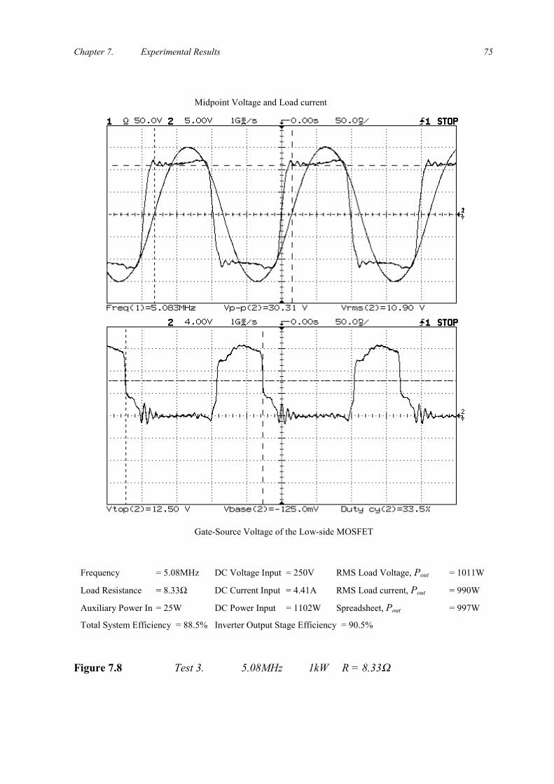
Chapter 7. Experimental Results 75
Midpoint Voltage and Load current
Gate-Source Voltage of the Low-side MOSFET
Frequency = 5.08MHz DC Voltage Input = 250V RMS Load Voltage, Pout = 1011W
Load Resistance = 8.33Ω DC Current Input = 4.41A RMS Load current, Pout = 990W
Auxiliary Power In = 25W DC Power Input = 1102W Spreadsheet, Pout = 997W
Total System Efficiency = 88.5% Inverter Output Stage Efficiency = 90.5%
Figure 7.8 Test 3. 5.08MHz 1kW R = 8.33Ω

Chapter 7. Experimental Results 76
Midpoint Voltage and Load current
Gate-Source Voltage of the Low-side MOSFET
Frequency = 5.71MHz DC Voltage Input = 260V RMS Load Voltage, Pout = 1044W
Load Resistance = 8.33Ω DC Current Input = 4.40A RMS Load current, Pout = 1003W
Auxiliary Power In = 26W DC Power Input = 1144W Spreadsheet, Pout = 1006W
Total System Efficiency = 86% Inverter Output Stage Efficiency = 88%
Figure 7.9 Test 4. 5.71MHz 1kW R = 8.33Ω

Chapter 7. Experimental Results 77
Frequency = 2.48MHz DC Voltage Input = 321V RMS Load Voltage, Pout =
Load Resistance = ~12.5Ω DC Current Input = 4.17A RMS Load current, Pout =
Auxiliary Power In = 23W DC Power Input = 1340W Spreadsheet, Pout = 1257W
Total System Efficiency = 92% Inverter Output Stage Efficiency = 93.8%
Midpoint Voltage and Load current
Gate-Source Voltage of the Low-side MOSFET
Figure 7.10 Test 5. 2.48MHz 1.25kW R ~ 12.5Ω

Chapter 7. Experimental Results 78
Frequency = 2.53MHz DC Voltage Input = 322V RMS Load Voltage, Pout =
Load Resistance = ~16.7Ω DC Current Input = 3.15A RMS Load current, Pout =
Auxiliary Power In = 23W DC Power Input = 1017W Spreadsheet, Pout = 959W
Total System Efficiency = 92% Inverter Output Stage Efficiency = 94.3%
Midpoint Voltage and Load current
Gate-Source Voltage of the Low-side MOSFET
Figure 7.11 Test 6. 2.53MHz 960W R ~ 16.7Ω
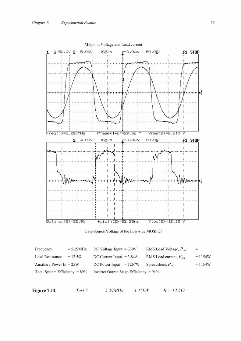
Chapter 7. Experimental Results 79
Frequency = 5.29MHz DC Voltage Input = 330V RMS Load Voltage, Pout =
Load Resistance = 12.5Ω DC Current Input = 3.84A RMS Load current, Pout = 1154W
Auxiliary Power In = 25W DC Power Input = 1267W Spreadsheet, Pout = 1154W
Total System Efficiency = 89% Inverter Output Stage Efficiency = 91%
Midpoint Voltage and Load current
Gate-Source Voltage of the Low-side MOSFET
Figure 7.12 Test 7. 5.29MHz 1.15kW R = 12.5Ω
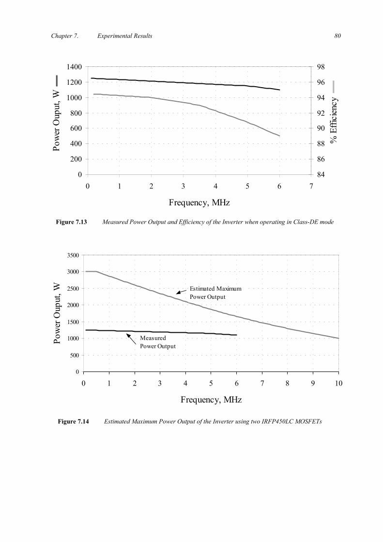
Chapter 7. Experimental Results 80
0
200
400
600
800
1000
1200
1400
0 1 2 3 4 5 6 7
Frequency, MHz
Pow
er O
uput
, W
84
86
88
90
92
94
96
98
% E
ffici
ency
Figure 7.13 Measured Power Output and Efficiency of the Inverter when operating in Class-DE mode
Figure 7.14 Estimated Maximum Power Output of the Inverter using two IRFP450LC MOSFETs
0
500
1000
1500
2000
2500
3000
3500
0 1 2 3 4 5 6 7 8 9 10
Frequency, MHz
Pow
er O
uput
, W
Measured Power Output
Estimated Maximum Power Output
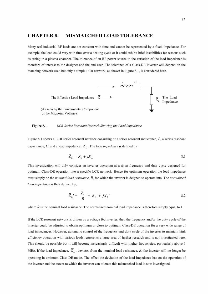
81
CHAPTER 8. MISMATCHED LOAD TOLERANCE
Many real industrial RF loads are not constant with time and cannot be represented by a fixed impedance. For
example, the load could vary with time over a heating cycle or it could exhibit brief instabilities for reasons such
as arcing in a plasma chamber. The tolerance of an RF power source to the variation of the load impedance is
therefore of interest to the designer and the end user. The tolerance of a Class-DE inverter will depend on the
matching network used but only a simple LCR network, as shown in Figure 8.1, is considered here.
Figure 8.1 shows a LCR series resonant network consisting of a series resonant inductance, L, a series resonant
capacitance, C, and a load impedance, LZ . The load impedance is defined by
LLL jXRZ += 8.1
This investigation will only consider an inverter operating at a fixed frequency and duty cycle designed for
optimum Class-DE operation into a specific LCR network. Hence for optimum operation the load impedance
must simply be the nominal load resistance, R, for which the inverter is deigned to operate into. The normalized
load impedance is then defined by,
''' LLL
L jXRR
ZZ +== 8.2
where R is the nominal load resistance. The normalized nominal load impedance is therefore simply equal to 1.
If the LCR resonant network is driven by a voltage fed inverter, then the frequency and/or the duty cycle of the
inverter could be adjusted to obtain optimum or close to optimum Class-DE operation for a very wide range of
load impedances. However, automatic control of the frequency and duty cycle of the inverter to maintain high
efficiency operation with various loads represents a large area of further research and is not investigated here.
This should be possible but it will become increasingly difficult with higher frequencies, particularly above 1
MHz. If the load impedance, LZ , deviates from the nominal load resistance, R, the inverter will no longer be
operating in optimum Class-DE mode. The effect the deviation of the load impedance has on the operation of
the inverter and the extent to which the inverter can tolerate this mismatched load is now investigated.
L C
The Effective Load Impedance ZLZ
(As seen by the Fundamental Component of the Midpoint Voltage)
The LoadImpedance
Figure 8.1 LCR Series Resonant Network Showing the Load Impedance

Chapter 8. Mismatched Load tolerance 82
8.1 IDEAL CLASS-D INVERTER
To investigate the effect of the load impedance, we will first consider an ideal Class-D voltage-fed series
resonant inverter. This drives the LCR circuit at resonance and the switches have no output capacitance and an
ideal reverse diode. The load current will simply be given by the fundamental component of the midpoint
voltage (always square) divided by the load impedance [3]. The only limitation of the load current in this case is
that it should not exceed a maximum value given by Imax. The load impedance should therefore not be less than
the value that gives rise this maximum load current, thus
maxL
sm I
ZV
I ≤=π2
Hencemax
sL I
VZ
π2
≥ 8.1.1
The region that this condition excludes can be seen on the normalized load impedance plane of Figure 8.2. For
an ideal Class-D inverter, the load impedance can therefore take on any value up to infinity (open circuit) except
for the shaded region shown in Figure 8.2. The power dissipated will always be zero and the efficiency will
always be 100%. The voltage stress on each switch will always only be the supply voltage, Vs. It can therefore
be seen that it is fundamentally a very robust topology.
RL'
jXL'
1 2
-j
0
-2j
j
2j
R'
Operation in
Shaded Areato be avoided
Figure 8.2 Normalized Load Impedance Plane showing the Range of Load ImpedancesTolerated by an Ideal Class-D Inverter

Chapter 8. Mismatched Load tolerance 83
8.2 PRACTICAL CLASS-D INVERTER
To feasibly operate an inverter in the conventional Class-D mode, the output capacitances of the switching
devices must have a negligible effect on the operation of the inverter. This will only happen if the switching
frequency is low enough so that the CV 2f losses are negligible, even with no load. Using currently available
MOSFETs, a half-bridge voltage-fed series resonant inverter can feasibly operate in the conventional Class-D
mode up to approximately a few hundred kHz. At higher frequencies, the capacitive switching loss will have to
be considered. However, even at low frequencies, a practical Class-D inverter using MOSFETs will have a
failure mode associated with the MOSFET's reverse integral diode. This diode has a maximum reverse recovery
dv/dt rating that cannot be exceeded as it will cause device failure. This will occur if the inverter is operating in
the capacitive mode and the MOSFETs are being hard switched. In the capacitive mode the inverter will be
driving the LCR network below resonance and have a leading load current. Hence the switch's diode will be
conducting at the end of the conduction period. If the MOSFETs are being hard-switched, then the dv/dt rating
of the integral reverse diode will be exceeded when the opposing switch turns-on and the device will fail. The
load impedance can therefore not have any capacitive reactance. In practice, however, the inverter will be
operating slightly above resonance and so some capacitive reactance will be tolerated, but this is not shown in
Figure 8.3. The load current may also not exceed a maximum value and so the same condition as with an ideal
Class-D inverter applies. Except for the shaded regions shown in Figure 8.3, all other reactive load impedances
will be tolerated up to infinity (open circuit). The voltage stress on each switch will always only be the supply
voltage, Vs. Assuming the capacitive switching losses are small, then the power dissipated should remain close
to the normal operating value for all the allowed load impedances. The tolerated range of load impedances can
be seen in the normalized load impedance plane of Figure 8.3.
RL'
jXL'
1 2
-j
0
-2j
j
2j
R'
Operation inShaded Areato be avoided
Figure 8.3 Normalized Load Impedance Plane showing the Range of Load ImpedancesTolerated by a Practical Class-D Inverter using MOSFETs

Chapter 8. Mismatched Load tolerance 84
8.3 THE CLASS-DE INVERTER
The term "Class-DE" is applied here to an inverter where the output capacitance cannot be neglected. It is also
referred to in the literature as a zero-voltage-switching (ZVS) Class-D series resonant inverter [54]. These
inverters must employ some means of reducing the capacitive switching losses. The mismatched load tolerance
of a Class-DE inverter will depend on a number of parameters and follows certain trends described below;
A higher output capacitance => Decreases the tolerance of an inverter as the capacitive switching
losses will be increased,
Increasing the switching frequency => Decreases the tolerance of an inverter as the capacitive switching
losses will be increased,
Increasing the impedance levels => Decreases the tolerance of an inverter as the higher supply voltage
implies increased capacitive switching losses,
Decreasing the conduction angle => Decreases the tolerance of an inverter as this implies either or all of
the following; a high output capacitance, a high switching frequency,
or high impedance levels.
The actual range of load impedances a Class-DE inverter can tolerate is difficult to specify exactly but general
guidelines can be investigated. This investigation will only consider a Class-DE inverter using MOSFETs. A
Class-DE inverter operating into its designed nominal LCR network will see an effective load impedance, as
defined in Section 2.2.3, defined by
jXRZ += 8.3.1
where R and X are given by equation (2.2.27) and equation (2.2.28) of Section 2.2.3. As the load impedance
varies away from its nominal load resistance, R, then the effective load impedance that the fundamental
component of the midpoint voltage will see is given by
jXZZ L += 8.3.2
The effect of the variation of the load impedance can now be investigated. If the load impedance's resistance
increases, then the load current will be decreased and the midpoint voltage will not swing all the way to the
opposite rail and capacitive switching losses will occur. This is illustrated in Figure 8.4 that shows the power
dissipation increasing with increasing load resistance. If the load impedance's resistance decreases, the load
current will increase and the midpoint voltage will swing past the opposite rail causing the diode to conduct at
the beginning of the conduction period (ZVS turn-on will occur). Assuming that the diode conduction at the
beginning of the conduction period has no adverse affects, then there will be no power dissipated in this region
of operation.
The effect of load reactance on the inverter is not so clear. As the reactance of load impedances varies it will
change the phase and magnitude of the load current. However, the actual shape of the midpoint voltage will be

Chapter 8. Mismatched Load tolerance 85
complicated due to the fact that the switches are operating with a duty cycle of less than 50%. The first
consideration is that as in a practical Class-D inverter, the dv/dt reverse recovery rating of the diode means the
inverter must not operate in the capacitive mode (diode conducting at the end of the conduction period). From
equation 8.3.2, we can make the intuitive deduction that the load impedance can have a capacitive reactance of
least up to -jX before the inverter will be operating in the capacitive mode. As the capacitive reactance of the
load impedance increases from zero to -jX, the capacitive switching losses will gradually increase reaching a
maximum at some point. At this point the MOSFETs will be turning on with the full supply voltage across them
and this represents the worst case of capacitive switching losses. The amount of capacitive reactance the inverter
can tolerate therefore depends on its power dissipation capability and this is illustrated in Figure 8.4. If the load
impedance's inductive reactance increases then the phase lag of the load current will increase and this will cause
the diode to conduct at the beginning of the conduction period (ZVS turn-on will occur). However, the
magnitude of an inductive load impedance may only increase to certain amount before the magnitude of the load
current is too small too swing the midpoint voltage all the way to the opposite rail. As in an ideal Class-D
inverter, the magnitude of load impedance cannot be less than a specific value, but this magnitude will include
the reactance jX, hence this circle will be centered around -jX'. These conditions are illustrated by the shaded
regions of Figure 8.4 which shows the range of load impedances tolerated by a Class-DE inverter in the
normalized load impedance plane.
From Figure 8.4 we can see that the inverter will tolerate a fairly large range of inductive load impedances while
still maintaining ZVS and hence have no power dissipation. Capacitive reactance will increase capacitive
switching losses and hence power dissipated. As in a Class-D inverter, the voltage stress on each switch will
RL'
jXL'
1 2
-j
0
-2j
j
2j
R'
-jX'
PD Increasing
PD Increasing
ZVS switchingOccurring in this region(i.e. No Power Dissipation)
Operation in
Shaded Areato be avoided
Figure 8.4 Normalized Load Impedance Plane showing the Range of Load ImpedancesTolerated by a Class-DE Inverter using MOSFETs

Chapter 8. Mismatched Load tolerance 86
always only be the supply voltage, Vs, for all load impedances. It should also be noted that mismatched load
tolerance depends to large extent on the power dissipation capability of the inverter. As a Class-DE inverter
should be operating very efficiently, it should have ample power dissipation capability in reserve. From this fact,
together with the results of Figure 8.4, it can be deduced that a Class-DE inverter should have a very good
mismatched load tolerance. However, Figure 8.4 only serves as a guide and more quantitative information can
be obtained by simulation on a program such as HB-Plus [57]. Ultimately the load tolerance of the inverter will
have to be determined experimentally.

87
CHAPTER 9. CONCLUSIONS
This thesis investigated the various aspects of the theory, design and construction of high frequency and high
power Class-DE type DC/AC inverters. From the analysis presented in Chapter 2 it can be seen that a Class-DE
inverter has a theoretical power advantage over a Class-E inverter up to approximately 6 MHz using standard
switch-mode type MOSFETs. The practical aspects of implementing a Class-DE inverter to work up to this
frequency were then investigated. It was found that a half-bridge type inverter was the most suitable topology,
as it does not fundamentally limit the operating power or frequency. The limiting factor will actually be the
switching devices themselves. The main practical problems of implementing a half-bridge inverter were found
to be the gate-drive, the physical construction of the inverter output stage, the generation of the control signals
and the communication-link to the high-side switch. The use of a fiber optic link as communication-link to the
high-side switch proved to be an excellent solution, enabling the inverter to be controlled from DC - 5 MHz. A
fiber optic communication link will not be a limiting factor to the maximum feasible operating power and
frequency of a Class-DE inverter. Generation of the control signals was suitably achieved for Class-DE type
operation from 50 kHz to 5 MHz. The implementation of a digital dead-time should enable suitable control
signals to be generated for Class-DE type operation over the entire HF band. The physical construction of the
inverter becomes more difficult with increasing frequency and power (i.e. less tolerance of stray impedance).
An innovative construction of the output stage of the inverter enabled very clean and discernible Class-DE type
operation to be achieved up to 5 MHz at a power level of 1 kW (with an operating impedance level of 10 Ω).
Hybrid circuit technology using ceramic substrates should enable a half-bridge inverter to be constructed with
low enough stray impedances for operation up to 13.56 MHz, and possibly for power levels of up to 10 kW.
Driving the gate capacitance directly with a suitably low impedance driver enabled the required rise and fall
times to be achieved, and for the MOSFETs to be driven from DC-5 MHz with any duty cycle. However, power
dissipation and the physical size of the gate-driver were problems. For higher operating frequencies new
techniques will have to be investigated to reduce the rise and fall times, increase the power dissipation capability
and reduce the physical size of the gate-driver circuitry.
The broadband design of the control circuitry, communication-link and gate-drive enabled the half-bridge
inverter output stage to be driven from 50 kHz through to 6 MHz. The half-bridge topology proved to be an
excellent solution as it enabled very clean and discernible waveforms to be observed that clearly showed
Class-DE operation. It also enabled the mechanism of the operation of the inverter to be ascertained for various
operating conditions. The broadband capability of the half-bridge enabled the inverter to produce RF power
from 50 kHz to 6 MHz with the only circuit changes needed for the different frequencies being the inductance
and capacitance of the tuned network. The design equations developed in Chapter 2 enabled simple and fast
calculation of the values of the inductance and capacitance. The ability to change the frequency and duty cycle
of the inverter made the tuning procedure for Class-DE operation relatively simple and as it could be achieved
without any circuit changes.
Chapter 9. Conclusions 88
When operated in the Class-DE mode, the inverter was found to be capable of delivering a power output of over
1 kW from 50 kHz to 1 MHz with an efficiency of 94%. This is fairly close to the theoretical maximum
efficiency determined by the on-resistance of the MOSFETs. The efficiency decreased slightly with increasing
frequency from 1 MHz to 5 MHz. The last test of the inverter produced 1.15kW of output power at 5.3 MHz
with an efficiency of 91%.
A comparison of the performance of various topologies is given below. All the topologies are using only two
IRFP450 MOSFETs and they experience the same peak voltage and current stresses. If the operating frequency
is 5 MHz, the peak voltage stress is 330V, and the peak current is 12.7A, then we have
• Class B and C Pout = ~ 450W η = ~ 60% PD = ~ 200W
(Power output limited by power dissipation capability)
• Class-DE Pout = 1150W η = 91% PD = 113W
• Class-E Pout = ~ 750W η = ~ 87-90% PD = ~ 100W
Where Pout is the output power, η is the efficiency and PD is the power dissipated. It can be seen from the
above results that a Class-DE inverter is capable of producing a higher combination of power and efficiency
than any other current topology up to a frequency of 5 MHz and at power levels of 1kW.
As the MOSFETs are being used as switching devices they may be connected in parallel relatively easily and
the variation of device parameters will have no adverse effects. Paralleling the switching MOSFETs can
increase the power output of a Class-DE inverter, but increasing the power will decrease the operating
impedance level and hence place tighter restrictions on the construction of the inverter. It is the author's opinion
that it should be possible to parallel more than five sets of MOSFETs at 5 MHz, thereby increasing power levels
to approximately 10kW. It is also the author's opinion that the operating frequency of a voltage-fed half-bridge
Class-DE inverter can be extended to cover the 13.56 MHz ISM band. The main practical problems will be the
gate-drive and physical construction. Above this frequency the advantages of a Class-DE topology over a
Class-E topology are limited and the development difficulties increase considerably.
A Class-DE type inverter could be used for many applications requiring RF power in the HF band, such as AM
or SW radio transmitters, induction heating and plasma generators. The information presented in this thesis will
be useful to designers wishing to implement such an inverter. A Class-DE type inverter also offers great
potential for use in a DC-DC converter. However a method of regulating the power flow (and hence output
voltage) while still maintaining zero voltage switching transitions (or as close as possible to optimum Class-DE
operation) remains to be investigated. Many principles of a Class-DE topology are similar to a Class-E
topology and hence the theory and information presented in this thesis will give a good introduction towards
understanding the more complex operation and equations of a Class-E topology.
Chapter 9. Conclusions 89
9.1 CLASS-DE VERSUS CLASS-E
The differences between Class-DE and Class-E are subtle compared to linear topologies, and the most suitable
topology will depend on mainly on the operating frequency; but factors such as the application, power levels
and development time also have to be considered. Class-D is most suited to frequencies from DC to a few
hundred kHz, Class-DE from above a few hundred kHz to a few MHz, and above this Class-E. The exact cross-
over points are somewhat ambiguous and will change with new technology. However, some general guidelines
are given below.
From the analysis of a Class-DE topology, it can be seen that it has a theoretical power advantage over a Class-E
topology for switch conduction angles greater than 104.4º (duty cycle of 29%). For a duty cycle of 29%, a
Class-DE topology has the same switch utilization factor as a Class-E topology (i.e. the same power output for a
given switch voltage and current stress). Thus if the duty cycle in a Class-DE inverter is required to be less than
29% it would produce less power than a Class-E. The duty-cycle required in a Class-DE inverter depends on the
output capacitance of the switches used and it decreases with increasing operating frequencies. One may then
calculate at what frequency the duty cycle required in a Class-DE inverter equals 29%.
However, the physical construction and practical problems of implementing a two switch Class-DE topology are
considerably larger than the single switch Class-E topology. Hence the duty cycle should be at least 35% or
more to in order justify the extra power gained through the use of a Class-DE topology over a Class-E topology.
The frequency at which the required duty cycle is 35% appears to be in the region of 10 to 15 MHz using the
high voltage and high power RF MOSFETs now offered by some manufacturers. Above this frequency the
switch utilization factor approaches that of a Class-E and there is little to be gained from a Class-DE topology
over a Class-E topology.
From the results of this thesis it can be seen that from 100kHz to 6 MHz a Class-DE topology is the best means
of producing raw RF power. Over this frequency range it offers the highest combination of output power and
efficiency and has a good mismatched load tolerance. It also preserves normal operating waveforms over a wide
range of load impedances. It is the author's opinion that this frequency can be extended to cover the 13.56 MHz
ISM band. However, it should be noted that a two switch Class-DE topology will require more development
time and effort than a single switch Class-E topology.

Chapter 9. Conclusions 90
9.2 ORIGINAL WORK
A summary of the original work presented in this thesis is given below.
• An analysis and description of Class-DE operation in a half-bridge inverter is presented. The concept of a
conduction angle is introduced which enables a more intuitive understanding of the analysis equations and
design equations developed thereafter. The effect of a non-linear output capacitance was studied and
equations are modified to take this effect into account. The design equations enable the conduction angle
required, power output and the circuit element values of the LCR network to be calculated simply and
quickly.
• The results of an investigation into the practical problems of implementing a high power and high
frequency Class-DE inverter, and guidelines to solving these problems, is presented. Some novel solutions
to these problems are developed and these solutions were implemented in a prototype voltage-fed half-
bridge inverter. These solutions enabled the feasible operation of a high power half-bridge inverter to be
extended up to 5 MHz, and were found to work very effectively. It is concluded that the practical problems
of implementing a half-bridge Class-DE inverter can be overcome with further development for operation
up to 13.56 MHz.
• The use of a fiber optic link as the means of communicating the drive signal to floating switches at high
frequencies and high powers is shown to be very feasible.
• Class-DE operation of a voltage-fed half-bridge series resonant inverter at various frequencies up to 5 MHz
and at power levels of 1kW is clearly shown.
• The results of this thesis prove that a Class-DE topology is capable of producing RF power up to a
frequency of 5 MHz with a higher combination of power and efficiency than any other current topology
operating with the same switch voltage and current stresses.
• A brief investigation of the mismatched load tolerance of a Class-DE inverter is presented.

91
APPENDIX A. Fundamental Component of the Midpoint Voltage
[ ]
[
[
[
+∈
∈−
∈
∈
=
s
ss
on
ons
m
Tttv
TtV
Ttttv
ttV
tv
2)(
,22
,)(
,02
)(
2
1
Where KdttIC
tv spo
+−= ∫ )sin(2
1)(1 ω
Integrating and using the boundary condition that 2
)(1s
onV
tv = , then
+−+
+=
φφω
φ cos1cos1
2)cos(
)cos1()(1
ss
s VtVtv
Similarly
+−−
+= ω
φ cos1cos1
2)cos(
)cos1()(2
ss
s Vt
Vtv
Conduction Angle = φ , Duty Cycle, πφ2
=D , ontωφ=
vm(t)
0 Ts /2
-Vs /2
Vs /2
ton
sωφ v1(t)
td
v2(t)
]
]
]
+
son
ons
s
Tt
tT
,
2
2
[ ]2, son Ttt ∈
we have
[ ]2, son Ttt ∈
φφ [ ]sons TtTt ,2 +∈
s ,
ssT
ωπ2
=
Tst

Appendix A. Fundamental Component of the Midpoint Voltage 92
The midpoint voltage may be expressed as a sum of the Fourier series of complex exponentials
∑∞=
−∞=
=n
n
tjnnm
seVtv ω)(
Where the complex Fourier series coefficients, nV , can be found using
∫ −=s
sT
tjnm
sn dtetv
TV
0)(1 ω
The first coefficient of the fundamental can be found by evaluating this integral for n=1.
Thus setting n=1, and expanding the integral
+−++= ∫∫∫∫ +
−+
−−−s
ons
sons
s
ss
on
son
s
T
tT
tjtT
T
tjsT
t
tjt
tjs
sdtetvdteVdtetvdteV
TV
22
2
2
2
10
1 )(2
)(2
1 ωωωω
Evaluating the integral, we have
( )[ ]φφφφπφπ
21 sincossin
)cos1(2j
VV s −+−
+=
1V can be expressed in polar form as
βjeVV 11 =
Where
φφφφπφπ
421 sin)cossin(
)cos1(2++−
+= sV
V
and
+−
−= −
φφφπφβ
cossinsintan
21
The fundamental component, vm1(t), of the midpoint voltage vm(t), is given by
tjtjm1
ss eVeVtv ωω −−+= 11)(
But for real functions of time, *11 VV =− , and so using the polar form of 1V , we have
tjjtjjm1
ss eeVeeVtv ωβωβ −−+= 11)(
[ ] [ ]tjtj ss eVeV ωβω1
)(1 2ReRe2 == +
)cos(2 1 βω += tV s

93
APPENDIX B. HB-PLUS SIMULATION RESULTS OF THEDESIGN EXAMPLE
Half-Bridge power amplifier/converter (HB) Jan. 10, 1999 12:55
Simulation of The Design Example
ENTER CIRCUIT PARAMETERS and TITLE SCREEN-1
Switching frequency (f)………………..[Hz]: 5E+06
DC supply voltage (Vcc or Vdd)…….[volts]: 300
Fraction of period, turn-on of Sw1 to Sw2…: 0.5
Switch 1 parameters
Duty ratio of switch 1...................………: 0.345
Ron1.............................………….[ohms]: 0.01
Roff1.............................…………[ohms]: 1E+06
Cout1..........................………….[farads]: 3.67E-10
Cout1 series resistance (Rcout1)..[ohms]: 0.001
Saturation offset voltage (Vo1).…[volts]: 0
Switch 2 parameters
Duty ratio of switch 2...................……..: 0.345
Ron2..............................………..[ohms]: 0.01
Roff2.............................………...[ohms]: 1E+06
Cout2...........................…………[farads]: 3.67E-10
Cout2 series resistance (Rcout2)..[ohms]: 0.001
Saturation offset voltage (Vo2).....[volts]: 0
ENTER CIRCUIT PARAMETERS SCREEN-2
Load resistance (Rload)...........……...[ohms]: 9.37
L2............................……………….[henries]: 1.23E-06
ESR_L2..........................……………[ohms]: 0.001
C2..............................………………[farads]: 1E-09
ESR_C2..........................……………[ohms]: 0.001
SELECTION: <,> ENTRY: ALPHANUM. EXECUTE: <PgDn> ABORT: <ESC>

Appendix B. HB-Plus Simulation Results of the Design Example 94
Half-Bridge power amplifier/converter (HB) Jan. 10, 1999 12:56
Simulation of The Design Example
EFFICIENCY AND POWERS
Collector/drain efficiency (Pout/Pin).……[%] 99.882
Collector/drain ineff'y (Pin-Pout)/Pin……[%] 0.11813
DC power input (Pin)..............……….[watts] 1204.2
Power output (Pout)...............………..[watts] 1202.8
Power loss in L2..................…………[watts] 0.12837
Power loss in C2..................…………[watts] 0.12837
Power loss in Ron1................………..[watts] 0.57754
Power loss in Rcout1..............……….[watts] 0.0054026
Power loss in Ron2................………..[watts] 0.57754
Power loss in Rcout2.............………..[watts] 0.0054026

95
APP
EN
DIX
C.
Dri
ve-S
igna
l-Gen
erat
or C
ircu
it
U3B
74AC
T109
16 8
15
13121410
11
9VCC GND
CLR
KCLK
JQ
PRE
Q
R4
39R
+5v
U11D
74HC
00
12 1311
C11
4.7u
F
U8
HFBR
-152
6
1 2 3 4
8 7 6 5
U2D 74
ACT1
4
98
U2B
74AC
T14
34
C522
0nF
U4B
74AC
T08
4 56
14 7
*
0
0
+5v
U5F
74AC
T14
1312
+5v
+5v
+5v
C722
0nF
+5v
U6C 74
ACT1
4
56
LED2
D1N5
806/
125C
+5v
U2A
74AC
T14
12
714
Dead
-tim
e ad
just
+5v
+5v
+5v
+5v
+5v
+5v
+5v
0
+5v
C333
0pF
+5v
0
0
+5v
0
+5v
LED1
D1N5
806/
125C
*+5
v
U5B 74
ACT1
4
34
714
U11B
74HC
00
4 56
714
Freq
uenc
y Ad
just
R10
1k
R12
10k
C922
0n
U4D
74AC
T08
13 1211
14 7
U5C 74
ACT1
4
56
+5v
+5v
R739R
0
U9 74HC
4020
816
10
9 7 5 4 6 13 12 14 15 1 2 3
11GND
VCC
CLK
QA
QD
QE QF
QG
QH QI
QJ
QK QL
QM QN
CLR
U7
HFBR
-152
6
1 2 3 4
8 7 6 5
Rang
e Ad
just
0
U6E 74
ACT1
4
1110
D1 D1N4
148
R8
10k
U4C
74AC
T08
10 98
U5D
74AC
T14
98
R910
k
+5v
C1 150p
F
R2
500R
star
t/sto
p
0
U2F 74
ACT1
4
1312
714
U6D 74
ACT1
4
98
+5v
0
0
Decr
ease
C4
to
C822
0n
0
C4
100p
F
C622
0nF
D5
D02C
Z5_6
R11
1k
R610
0R
U4A
74AC
T08
1 23
R15
36.5
R
star
t/sto
p
U6F
74AC
T14
1312
R510
0R
R13
56R
U6B
74AC
T14
34
714
U5E
74AC
T14
1110
U10
CD40
24A
1
2
12 11 9 6 5 4 3
14 7
INPU
T RESETQ1
Q2
Q3
Q4
Q5
Q6
Q7VDD VSS
U2C
74AC
T14
56
714
C10 10
0uF
incr
ease
freq
uenc
y
D4
D02C
Z5_6
U11C
74HC
00
9 108
714
* U1
74LS
624
79
6 8
5 2 3 413
14 1
GNDVCC
Y Z
EN RN
G
CX1
CX2
FC
OSCPWR OSCGND
+5v
C233
0pF
0
R14
36.5
R

96
APP
EN
DIX
C.
Gat
e-D
rive
r C
ircu
it
Tant
alum
s
C7
220n
F * 8
+5v
+15V
R10
1k
R14
47k
+15V
+15V
+15V
R2 10k
U16
HFBR
-252
6
5 6 7 8
4 3 2 1
pin5
pin6
pin7
gnd8
V+
pin3 gn
d
sign
al
C822
0nF
+5v
+15V
D6BZ
-150
O
U5EL71
04CN
1 2 3 4
8 7 6 5
V+ In NC
gnd
V+.
Pout
Nou
t
gnd.
D7
D02C
Z3_9
C222
0nF*
4
C322
0nF*
4
C11
3.3u
F
R9 1kU1
4 LM78
05C
13
2
INO
UT
GND
R12
10k
O
U4EL71
04CN
1 2 3 4
8 7 6 5
V+ In NC
gnd
V+.
Pout
Nou
t
gnd.
+15V
C15
220n
F
C13
220n
F * 4
O
U6EL71
04CN
1 2 3 4
8 7 6 5
V+ In NC
gnd
V+.
Pout
Nou
t
gnd.
_
U2
LT10
16A
2 3
46
8 7 5
1
+ -
V-gnd
Q. Q LE
V+
D5BZ
-150
R5 249k
LED
D1N5
806/
125C
D8 BZ-0
56
+5v
+15V
R15 47
+5v
X1 C106
MR81k
Q1
MPS
2907
+15V
R1 332k
C12.
2nF
C422
0nF*
4
R4150k
R11
10k
+15V
R13 2k
C622
0nF*
4
C16
220n
F
C12
3.3u
F
+15V
U15
LM31
17
2 31
8 4
6
5 OU
T
+ -G
V+ V-
B/S
B
O
U3EL71
04CN
1 2 3 4
8 7 6 5
V+ In NC
gnd
V+.
Pout
Nou
t
gnd.

97
APPENDIX D. Design Equations of a Half-Bridge Class-DE Inverter
A summary of the equations used and procedure followed when designing a Half-bridge Class-DE inverter is
given below. The designer must first specify the desired supply voltage, Vs, the peak current through the
devices, Ip, the output capacitance of the devices, Co, and the switching frequency, fs. Alternatively, if the
output capacitance is non-linear, then the total charge QT required to charge the output capacitance to Vs must
be specified. The effective output capacitance can then be found as, s
Teffo V
QC =− . The required conduction
angle can then be calculated using the appropriate equation below (where ss fπω 2= )
12
cos −=p
sos
IVCωφ 1
2cos −=
p
Ts
IQωφ 1
2cos −= −
p
seffos
IVCω
φ
The required duty cycle of the switches and power output of the inverter will then be given by
πφ
2=D ( )φ
πcos1
2−= ps
out
IVP
The phase lag, α , between the fundamental component of the midpoint voltage and the midpoint current can be
found using the expression
+−=φ
φφφπα 2sincossintan
The designer must now select the desired value of the Q of the resonant LCR network (usually in the region of 3
to 5). The natural resonant frequency of the LCR network can then be found using
−+
=
QQf
f sr
αα tan4tan2
2
Using this value of the natural resonant frequency, the value of the resistance, inductance and capacitance in the
LCR network can be found using the following three expressions (where rr fπω 2= )
( )φπ
cos1 −=p
s
IV
Rr
RQLω
=RQL
Crr ωω11
2 ==
The Average current and RMS current through each switch will be
( )φπ
cos12
−=−p
avgS
II
πφφ
2)2sin2(
2−
=−p
rmsS
II

Appendix D. Design Equations of a Half-Bridge Class-DE Inverter 98
The maximum dv/dt experienced by each switch and the switch utilization factor will be
)sin(2
φo
p
MAX CI
dtdv = ( )φ
πcos1
41 −=U
If a more complex matching circuit is to be used other than a simple LCR network, such as tapped inductor or
tapped capacitor network, then the effective load impedance required by the inverter can be used to calculate the
circuit element values. The effective load impedance that the fundamental component of the midpoint voltage
must see is given by
jXRZ +=
where R is the real part of the effective load impedance and X is the reactive part (inductive). R and X can be
found using the following expressions
( )φπ
cos1 −=p
s
IV
R
++−=
φφφφπ
π cos1cossin
p
s
IV
X

99
REFERENCES
[1] P.J. Baxandall, “Transistor sine-wave LC oscillators”, Proceedings of the IEE, vol. 106, part B,supplement 16, pp.748-758, 1959
[2] H.L. Krauss, C.W. Bostian and F.H. Raab, Solid State Radio Engineering. John Wiley & Sons, 1981.
[3] M.K. Kazimierczuk, “Class-D voltage switching MOSFET power amplifier”, IEE Proceedings-B, Vol.38, No. 6, Nov. 1991.
[4] N.O. Sokal and A.D. Sokal, “Class-E – A New Class of High-Efficiency Tuned Single-EndedSwitching Amplifier”, IEEE J. Solid-State Circuits, vol. 10, no. 3, pp.168-176, June 1975
[5] Sayed-Amr El-Hamamsy, “Design of High Efficiency RF Class-D Amplifier”, IEEE Transactions onPower Electronics, Vol. 9, No. 3, pp. 297-308, May 1994.
[6] D.C. Hamill, “Impedance Plane Analysis of a Class-DE Amplifier”, Electronics Letters, Vol. 30, No.23, pp. 1905-1906, 10th November 1994.
[7] H. Koizumi, T. Suetsugu, M. Fujii, K.Shinhoda, S. Mori and K. Ikeda, “Class-DE High EfficiencyTuned Power Amplifier”, IEEE Trans. on Circuits and Systems, Part I, vol. 43, no. 1, pp.51-60, Jan.1996.
[8] D.C. Hamill, “Class-DE Inverters and Rectifiers for DC-DC Conversion”, Power ElectronicsSpecialists Conference, Baveno, Italy, June 1996.
[9] D.R.H. Carter, Aspects of High Frequency Half-Bridge Circuits. Ph.D. thesis, Cambridge University,Electrical Engineering Department, 1996
[10] F.H. Raab, “Idealized Operation of the Class-E Tuned Power Amplifier”, IEEE Trans. on Circuits andSystems, Vol. CAS-43, no. 12, pp.725-735, Dec. 1977.
[11] B.J. Baliga, “Power Semiconductor figure of Merit for High-Frequency Applications”, IEEE ElectronDevice Letters, Vol. 10, No. 10, pp. 455-457, October 1989.
[12] D.A. Grant and J. Gower, Power MOSFETS: Theory and Applications. Wiley Interscience, 1989.
[13] M.J. Chudobiak, “The Use of Parasitic Nonlinear Capacitors in Class-E Amplifiers”, IEEE Trans. onCircuits and Systems, Part I, vol. 41, no. 12, pp.941-944, Dec. 1994.
[14] M.K. Kazimierczuk and T. Nandakumar, “Class-D voltage switching inverter with a tapped resonantinductor”, IEE Proceedings-B, Vol. 140, No. 3, May. 1993.
[15] N.O. Sokal and I. Novak, “Resonant Power Converters: Computer-aided Predication of Voltage-Control Function, Transfer Functions and Avoidance of control-loop lock-up”, High Frequency powerConversion conference, Toronto, ON, Canada, June 1991.
[16] S. Hinchliffe and L. Hobson, “Review of solid state devices and circuits for HF electric process heatingapplications – Part I: devices”, Int. J. of Electronics, Vol. 61, No. 2, pp. 143-167, 1986.
[17] S. Hinchliffe and L. Hobson, “Review of solid state devices and circuits for HF electric process heatingapplications – Part II: circuits ”, Int. J. of Electronics, Vol. 61, No. 3, pp. 261-279, 1986.
[18] S. Hinchliffe, L. Hobson and R.W. Houston, “A high power Class-E amplifier for high frequencyprocess heating”, Int. J. of Electronics, Vol. 64, No. 4, pp. 667-675, 1988.

References 100
[19] S. Hinchliffe and L. Hobson, “High frequency switching of power MOSFETS”, Int. J. of Electronics,Vol. 65, pp. 127-138, 1988.
[20] S. Hinchliffe and L. Hobson, “High-frequency (>1MHz) converters for induction heating applications”,Electronics Letters, Vol. 24, No. 11, pp. 697-698, 26th May 1988.
[21] S. Hinchliffe and L. Hobson, “High Power Class-E amplifier for high frequency induction heatingapplications”, Electronics Letters, Vol. 24, No. 14, pp. 697-698, 7th July 1988.
[22] S. Hinchliffe, K. Thomas and L. Hobson, “High efficiency power source for HF electric processheating applications”, Int. J. Electronics, Vol. 63, No. 1, pp. 117-122, 1987.
[23] M.K. Kazimierczuk, “High-Speed Driver for Switching Power MOSFETS”, IEEE Trans. on Circuitsand Systems, vol. 35, no. 2, pp.254-256, Feb. 1988
[24] D.R.H. Carter and R.A. McMahon, “Electronic level shifter for use in half-bridges operating at13.56MHz”, Electronics Letters, Vol. 31, No. 16, pp. 1301-1302, 3rd August 1995.
[25] D.C. Hamill, “Half-Bridge Class-DE Rectifier”, Electronics Letters, Vol. 31, No. 22, pp. 1885-1886,26th October 1995.
[26] I.D. de Vries, J.H. van Nierop and J.R. Greene, “Solid-State Class-DE RF Power Source”, InProceedings of ISIE’98, Pretoria, South Africa, vol. 2, pp. 524-529, July 1998.
[27] S.A. Zhukov and V.B. Kozyrez, “Push-pull switching generator without switching loss” (in Russian),Poluprovodnikovye Pribory v Tekhnike Electrosvyazi (Semiconductor Devices in ElectricalCommunication Technology), vol. 15, pp. 95-107, 1975.
[28] N. Dye and H. Granberg, Radio Frequency Transistors: Principles and Applications. Butterworth-Heinemanne 1994.
[29] IR Application Note AN-937: Gate Drive characteristics and Requirements for HEXFETS.International Rectifier Corporation , 1995.
[30] S. Clemente and A. Dubashi, IR Application Note AN-978: HV Floating MOS-Gate Driver ICs,International Rectifier Corporation, 1995.
[31] HEXFET Designers Manual HDM-1, International Rectifier Corporation, 1993.
[32] W.J. Chudobiak and D.F. Page, “Frequency and Power limitations of Class-D Transistor Amplifiers”,IEEE Journal of Solid-State Circuits , Vol. SC-4, no. 1, pp.25-37, Feb. 1969.
[33] P. Senak, “Amplitude Modulation of the Switched-Mode Tuned Power Amplifier”, Proceedings ofIEEE, vol. 53, pp.1658-1659, October 1965.
[34] R. Severns and J. Armijos, MOSPOWER Applications Handbook, Siliconix Inc., 1985.
[35] N. Morrison, Introduction to Fourier Analysis, John Wiley and Sons Inc., 1994.
[36] R.J. Leedham, High Frequency Switching with Power MOSFETs. Ph.D. thesis, Cambridge University,Engineering Department, 1995.
[37] F. H. Raab, “The Class BD High-Efficiency RF Power Amplifier”, IEEE Journal of Solid-StateCircuits, vol. SC-12, no. 3, pp.291-298, June 1977
[38] H.O. Granberg, Broadband Transformers and Power Combining Techniques for RF, MotorolaApplication Note AN749, Motorola.

References 101
[39] H. Granberg, “Applying Power MOSFETs in Class D/E RF Power Amplifier Design”, MotorolaApplication Note AR141, Motorola. Reprinted from RF DESIGN, June, 1985.
[40] H. Granberg, “Good RF Construction Practices and Techniques”, Motorola Application Note AR164,Motorola. Reprinted from RF DESIGN, September, 1980.
[41] N. Dye and H. Granberg, “Using RF Transistors: Power Construction Techniques”, Electronics World+ Wireless World, March 1994.
[42] HP Application Note 1045, High-Speed Fiber-Optic Link, Hewlett Packard, 1991.
[43] M.K. Kazimierczuk, “Analysis of a Class-E Zero-Voltage-Switching Rectifier”, IEEE Trans. onCircuits and Systems, vol. 37, no. 6, pp.747-755, June 1990
[44] R.L. Steigerwald, “High-Frequency Resonant Transistor DC-DC Converters”, IEEE Trans. onIndustrial Electronics, vol. IE-31, no. 2, pp.181-191, May 1984
[45] R.L. Steigerwald, “A Comparison of Half-Bridge Resonant Converter Topologies”, IEEE Trans. onPower Electronics, vol. 3, no. 2, pp.174 -182, April 1988
[46] F. H. Raab, “Low Cost High-Efficiency HF Power Amplifiers, ” Proc. Nordic Shortwave Conf., Fårö,Sweden, August 1998.
[47] F. H. Raab and D.J. Rupp, “Quasi-complementary Class-D HF Power Amplifier, ” RF Design, vol. 15,no. 9, pp. 103-110, Sept. 1992.
[48] F. H. Raab and D.J. Rupp, “HF Power Amplifier operates in both Class-B and Class-D”, Proc. RFExpo West '93, San Jose, CA, pp. 114 -124, March 1993. [TP92-7]
[49] G.J. Krausse, “Advanced Power MOSFET generates 1kW RF power in the HF band,” Proc. RF ExpoWest '93, San Jose, CA, pp. 81-87, March 1993. [P-249]
[50] M.K. Kazimierczuk, W. Szaraniec, and S. Wang, “Analysis and Design of a parallel resonant converterat high QL ”, IEEE Trans. on Aerospace and Electronic Systems, vol. 28, pp. 35-49, January 1992.
[51] M.K. Kazimierczuk and S. Wang, “Frequency-domain Analysis of a series resonant converter forcontinuous conduction mode, ” IEEE Trans. on Power Electronics, vol. 7, pp. 270-279, April 1992.
[52] M.K. Kazimierczuk and W. Szaraniec, “Class-D zero-voltage-switching inverter with only one shuntcapacitor, ” em IEEE Proc. Part B, Electric Power Applications, vol. 139, pp. 449-456, September.
[53] M.K. Kazimierczuk and D. Czarkowski, Resonant Power Converters , John Wiley & Sons, 1981.
[54] D. Czarkowski and M.K. Kazimierczuk, “ZVS Class-D series resonant inverter - Discrete-time state-space simulation and experimental results, ” IEEE Trans. on Circuits and Systems, vol. 11, pp. 1141-1147, June 1990.
[55] T.B. Mader, “Quasi-optical Class-E power amplifiers, ” Ph.D. Dissertation, University of Colorado,Boulder, 1995.
[56] N.O. Sokal, “Classes A through S - How they operate, and when to use Each, ” Available from DesignAutomation, Inc. 4 Tyler Road, Lexington, MA.
[57] HB-Plus Simulation Program, available from Design Automation, Inc. 4 Tyler Road, Lexington, MA.