High Performance CMOS MEMS...
30
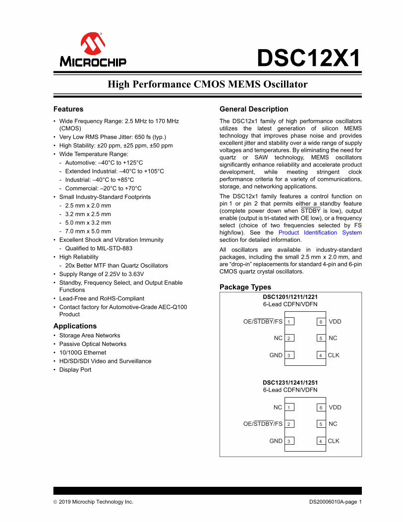
2019 Microchip Technology Inc. DS20006010A-page 1 DSC12X1 Features • Wide Frequency Range: 2.5 MHz to 170 MHz (CMOS) • Very Low RMS Phase Jitter: 650 fs (typ.) • High Stability: ±20 ppm, ±25 ppm, ±50 ppm • Wide Temperature Range: - Automotive: –40°C to +125°C - Extended Industrial: –40°C to +105°C - Industrial: –40°C to +85°C - Commercial: –20°C to +70°C • Small Industry-Standard Footprints - 2.5 mm x 2.0 mm - 3.2 mm x 2.5 mm - 5.0 mm x 3.2 mm - 7.0 mm x 5.0 mm • Excellent Shock and Vibration Immunity - Qualified to MIL-STD-883 • High Reliability - 20x Better MTF than Quartz Oscillators • Supply Range of 2.25V to 3.63V • Standby, Frequency Select, and Output Enable Functions • Lead-Free and RoHS-Compliant • Contact factory for Automotive-Grade AEC-Q100 Product Applications • Storage Area Networks • Passive Optical Networks • 10/100G Ethernet • HD/SD/SDI Video and Surveillance • Display Port General Description The DSC12x1 family of high performance oscillators utilizes the latest generation of silicon MEMS technology that improves phase noise and provides excellent jitter and stability over a wide range of supply voltages and temperatures. By eliminating the need for quartz or SAW technology, MEMS oscillators significantly enhance reliability and accelerate product development, while meeting stringent clock performance criteria for a variety of communications, storage, and networking applications. The DSC12x1 family features a control function on pin 1 or pin 2 that permits either a standby feature (complete power down when STDBY is low), output enable (output is tri-stated with OE low), or a frequency select (choice of two frequencies selected by FS high/low). See the Product Identification System section for detailed information. All oscillators are available in industry-standard packages, including the small 2.5 mm x 2.0 mm, and are “drop-in” replacements for standard 4-pin and 6-pin CMOS quartz crystal oscillators. Package Types DSC1201/1211/1221 6-Lead CDFN/VDFN 1 OE/STDBY/FS NC GND 6 VDD NC CLK 5 4 2 3 DSC1231/1241/1251 6-Lead CDFN/VDFN 1 OE/STDBY/FS NC GND 6 VDD NC CLK 5 4 2 3 High Performance CMOS MEMS Oscillator
Transcript of High Performance CMOS MEMS...
2019 Microchip Technology Inc. DS20006010A-page 1
DSC12X1
Features
• Wide Frequency Range: 2.5 MHz to 170 MHz (CMOS)
• Very Low RMS Phase Jitter: 650 fs (typ.)
• High Stability: ±20 ppm, ±25 ppm, ±50 ppm
• Wide Temperature Range:
- Automotive: –40°C to +125°C
- Extended Industrial: –40°C to +105°C
- Industrial: –40°C to +85°C
- Commercial: –20°C to +70°C
• Small Industry-Standard Footprints
- 2.5 mm x 2.0 mm
- 3.2 mm x 2.5 mm
- 5.0 mm x 3.2 mm
- 7.0 mm x 5.0 mm
• Excellent Shock and Vibration Immunity
- Qualified to MIL-STD-883
• High Reliability
- 20x Better MTF than Quartz Oscillators
• Supply Range of 2.25V to 3.63V
• Standby, Frequency Select, and Output Enable Functions
• Lead-Free and RoHS-Compliant
• Contact factory for Automotive-Grade AEC-Q100 Product
Applications• Storage Area Networks
• Passive Optical Networks
• 10/100G Ethernet
• HD/SD/SDI Video and Surveillance
• Display Port
General Description
The DSC12x1 family of high performance oscillatorsutilizes the latest generation of silicon MEMStechnology that improves phase noise and providesexcellent jitter and stability over a wide range of supplyvoltages and temperatures. By eliminating the need forquartz or SAW technology, MEMS oscillatorssignificantly enhance reliability and accelerate productdevelopment, while meeting stringent clockperformance criteria for a variety of communications,storage, and networking applications.
The DSC12x1 family features a control function onpin 1 or pin 2 that permits either a standby feature(complete power down when STDBY is low), outputenable (output is tri-stated with OE low), or a frequencyselect (choice of two frequencies selected by FShigh/low). See the Product Identification Systemsection for detailed information.
All oscillators are available in industry-standardpackages, including the small 2.5 mm x 2.0 mm, andare “drop-in” replacements for standard 4-pin and 6-pinCMOS quartz crystal oscillators.
Package TypesDSC1201/1211/12216-Lead CDFN/VDFN
1OE/STDBY/FS
NC
GND
6 VDD
NC
CLK
5
4
2
3
DSC1231/1241/12516-Lead CDFN/VDFN
1
OE/STDBY/FS
NC
GND
6 VDD
NC
CLK
5
4
2
3
High Performance CMOS MEMS Oscillator

DSC12X1
DS20006010A-page 2 2019 Microchip Technology Inc.
Functional Block DiagramsDSC1201/1211/1221
DSC1231/1241/1251
DIGITAL CONTROL
SUPPLY REGULATION
PLL
MEMS RESONATOR
TEMP SENSOR + CONTROL &
COMPENSATION
OUTPUT DIV
Pin 1OE/STDBY/FS
Pin 2NC
Pin 3GND
Pin 6VDD
Pin 5NC
Pin 4CLK
DIGITAL CONTROL
SUPPLY REGULATION
PLL
MEMS RESONATOR
TEMP SENSOR + CONTROL &
COMPENSATION
OUTPUT DIV
Pin 2OE/STDBY/FS
Pin 1NC
Pin 3GND
Pin 6VDD
Pin 4CLK+
Pin 5NC
2019 Microchip Technology Inc. DS20006010A-page 3
DSC12X1
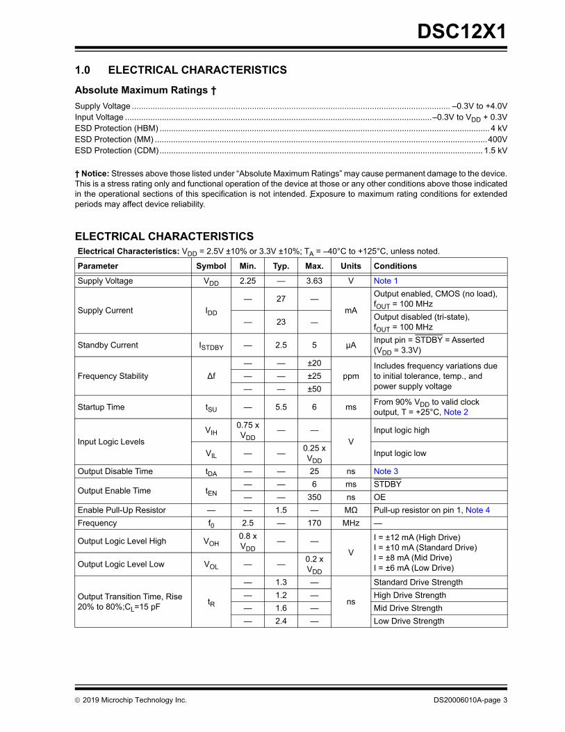
1.0 ELECTRICAL CHARACTERISTICS
Absolute Maximum Ratings †
Supply Voltage .......................................................................................................................................... –0.3V to +4.0VInput Voltage .....................................................................................................................................–0.3V to VDD + 0.3VESD Protection (HBM) ............................................................................................................................................... 4 kVESD Protection (MM) ................................................................................................................................................400VESD Protection (CDM)............................................................................................................................................ 1.5 kV
† Notice: Stresses above those listed under “Absolute Maximum Ratings” may cause permanent damage to the device.This is a stress rating only and functional operation of the device at those or any other conditions above those indicatedin the operational sections of this specification is not intended. Exposure to maximum rating conditions for extendedperiods may affect device reliability.
ELECTRICAL CHARACTERISTICSElectrical Characteristics: VDD = 2.5V ±10% or 3.3V ±10%; TA = –40°C to +125°C, unless noted.
Parameter Symbol Min. Typ. Max. Units Conditions
Supply Voltage VDD 2.25 — 3.63 V Note 1
Supply Current IDD
— 27 —mA
Output enabled, CMOS (no load), fOUT = 100 MHz
— 23 —Output disabled (tri-state), fOUT = 100 MHz
Standby Current ISTDBY — 2.5 5 µAInput pin = STDBY = Asserted (VDD = 3.3V)
Frequency Stability ∆f
— — ±20
ppmIncludes frequency variations due to initial tolerance, temp., and power supply voltage
— — ±25
— — ±50
Startup Time tSU — 5.5 6 msFrom 90% VDD to valid clock output, T = +25°C, Note 2
Input Logic LevelsVIH
0.75 x VDD
— —V
Input logic high
VIL — —0.25 x VDD
Input logic low
Output Disable Time tDA — — 25 ns Note 3
Output Enable Time tEN— — 6 ms STDBY
— — 350 ns OE
Enable Pull-Up Resistor — — 1.5 — MΩ Pull-up resistor on pin 1, Note 4
Frequency f0 2.5 — 170 MHz —
Output Logic Level High VOH0.8 x VDD
— —V
I = ±12 mA (High Drive)I = ±10 mA (Standard Drive)I = ±8 mA (Mid Drive)I = ±6 mA (Low Drive)Output Logic Level Low VOL — —
0.2 x VDD
Output Transition Time, Rise20% to 80%;CL=15 pF
tR
— 1.3 —
ns
Standard Drive Strength
— 1.2 — High Drive Strength
— 1.6 — Mid Drive Strength
— 2.4 — Low Drive Strength
DSC12X1
DS20006010A-page 4 2019 Microchip Technology Inc.
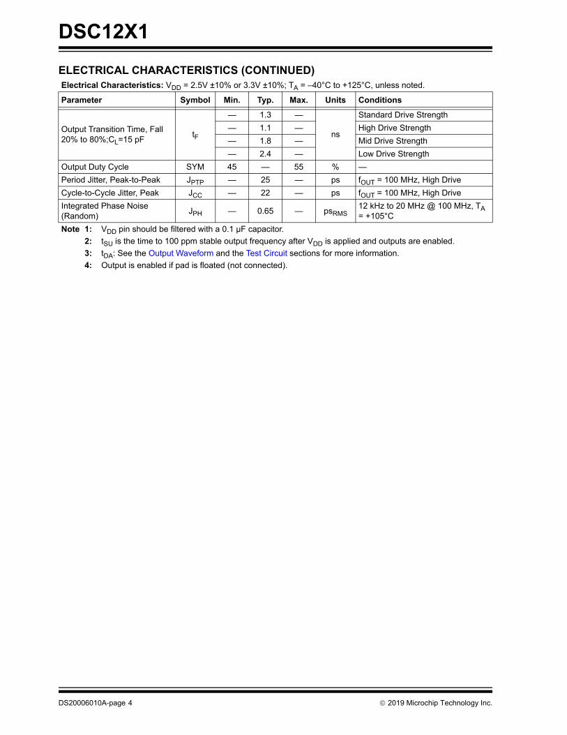
Output Transition Time, Fall20% to 80%;CL=15 pF
tF
— 1.3 —
ns
Standard Drive Strength
— 1.1 — High Drive Strength
— 1.8 — Mid Drive Strength
— 2.4 — Low Drive Strength
Output Duty Cycle SYM 45 — 55 % —
Period Jitter, Peak-to-Peak JPTP — 25 — ps fOUT = 100 MHz, High Drive
Cycle-to-Cycle Jitter, Peak JCC — 22 — ps fOUT = 100 MHz, High Drive
Integrated Phase Noise (Random)
JPH — 0.65 — psRMS12 kHz to 20 MHz @ 100 MHz, TA = +105°C
Note 1: VDD pin should be filtered with a 0.1 µF capacitor.
2: tSU is the time to 100 ppm stable output frequency after VDD is applied and outputs are enabled.
3: tDA: See the Output Waveform and the Test Circuit sections for more information.
4: Output is enabled if pad is floated (not connected).
ELECTRICAL CHARACTERISTICS (CONTINUED)Electrical Characteristics: VDD = 2.5V ±10% or 3.3V ±10%; TA = –40°C to +125°C, unless noted.
Parameter Symbol Min. Typ. Max. Units Conditions
2019 Microchip Technology Inc. DS20006010A-page 5
DSC12X1
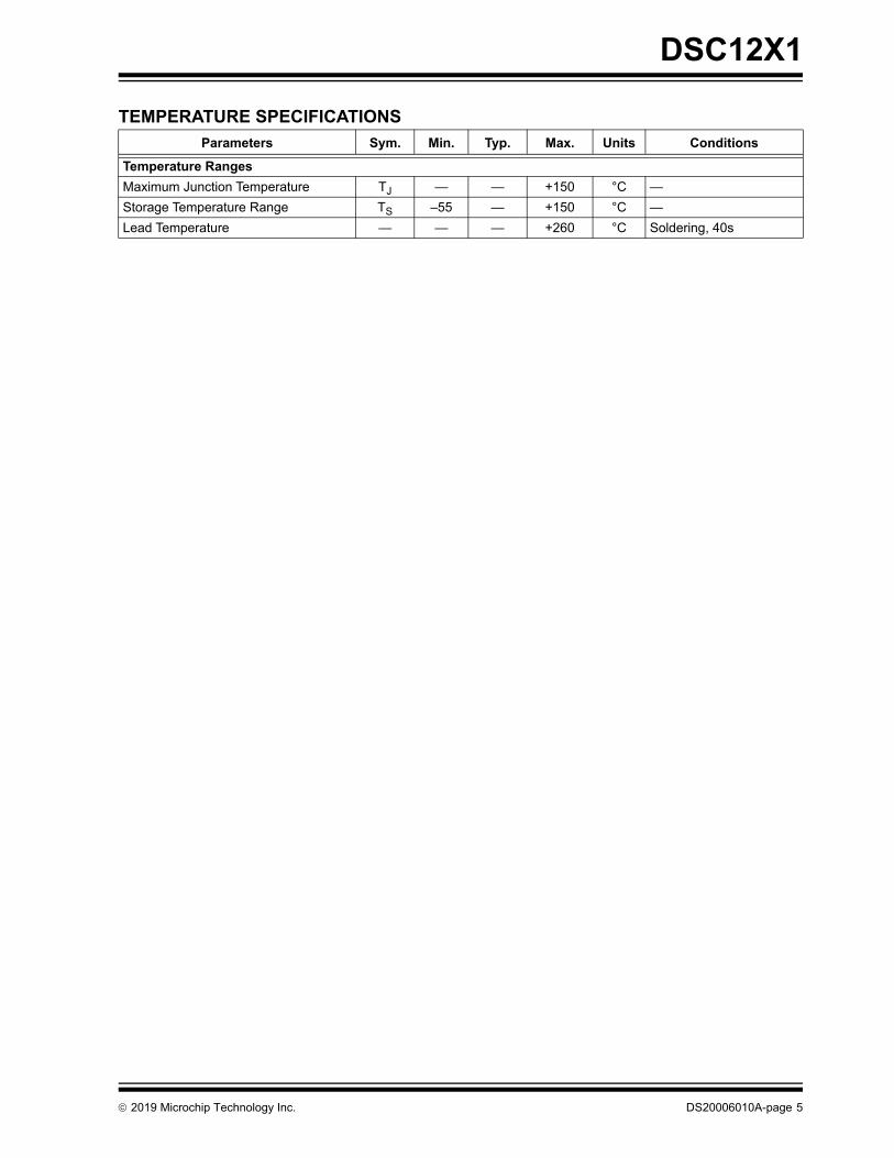
TEMPERATURE SPECIFICATIONS
Parameters Sym. Min. Typ. Max. Units Conditions
Temperature Ranges
Maximum Junction Temperature TJ — — +150 °C —
Storage Temperature Range TS –55 — +150 °C —
Lead Temperature — — — +260 °C Soldering, 40s

DSC12X1
DS20006010A-page 6 2019 Microchip Technology Inc.
2.0 PIN DESCRIPTIONS
The descriptions of the pins are listed in Table 2-1 and Table 2-2.
2.1 Standby
Complete power down when STDBY is low.
2.2 Frequency Select
Two frequencies may be chosen, selected by FS =High or Low. Please use the ClockWorks tool tocustomize frequencies.
2.3 Output Enable
Output buffers (only) are tri-stated when OE is low.
TABLE 2-1: DSC1201/1211/1221 PIN FUNCTION TABLE
Pin NumberDSC1201 DSC1211 DSC1221
Pin Name Description Pin Name Description Pin Name Description
1 STDBY Standby. FS Frequency select. OE Output enable.
2 NC No connect. NC No connect. NC No connect.
3 GNDPower supply ground.
GNDPower supply ground.
GNDPower supply ground.
4 CLK Clock output. CLK Clock output. CLK Clock output.
5 NC No connect. NC No connect. NC No connect.
6 VDD Power supply. VDD Power supply. VDD Power supply.
TABLE 2-2: DSC1231/1241/1251 PIN FUNCTION TABLE
Pin NumberDSC1231 DSC1241 DSC1251
Pin Name Description Pin Name Description Pin Name Description
1 NC No connect. NC No connect. NC No connect.
2 STDBY Standby. FS Frequency select. OE Output enable.
3 GNDPower supply ground.
GNDPower supply ground.
GNDPower supply ground.
4 CLK Clock output. CLK Clock output. CLK Clock output.
5 NC No connect. NC No connect. NC No connect.
6 VDD Power supply. VDD Power supply. VDD Power supply.
2019 Microchip Technology Inc. DS20006010A-page 7
DSC12X1
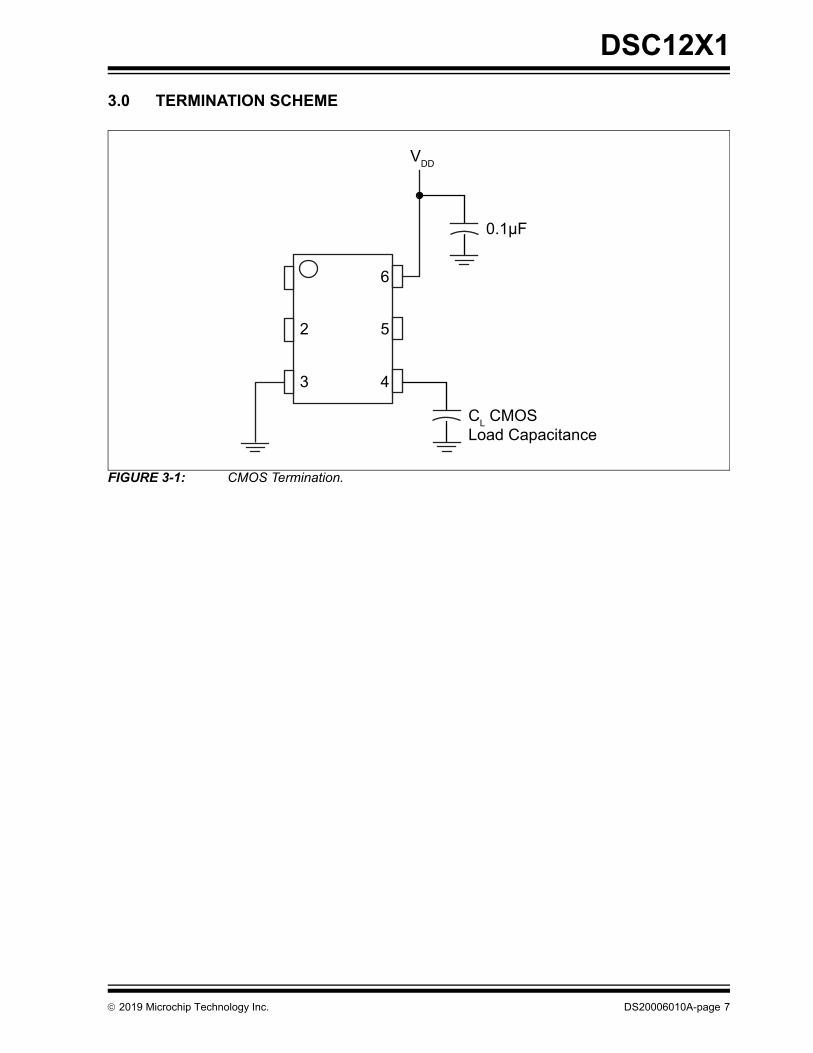
3.0 TERMINATION SCHEME
FIGURE 3-1: CMOS Termination.
2
3 4
5
6
VDD
0.1μF
CL CMOSLoad Capacitance

DSC12X1
DS20006010A-page 8 2019 Microchip Technology Inc.
4.0 OUTPUT WAVEFORM
FIGURE 4-1: CMOS Output Waveform.
TABLE 4-1: OUTPUT VOLTAGE SWING BY LOGIC TYPE
Output Logic Protocol Typical Peak-to-Peak Output Swing
CMOS VOH, VOL
Enable
tR tF
1/f0
tDA
tEN
VIL
VIH
50%
20%
80%
Output
Output voltage swing.Refer to table below.
2019 Microchip Technology Inc. DS20006010A-page 9
DSC12X1
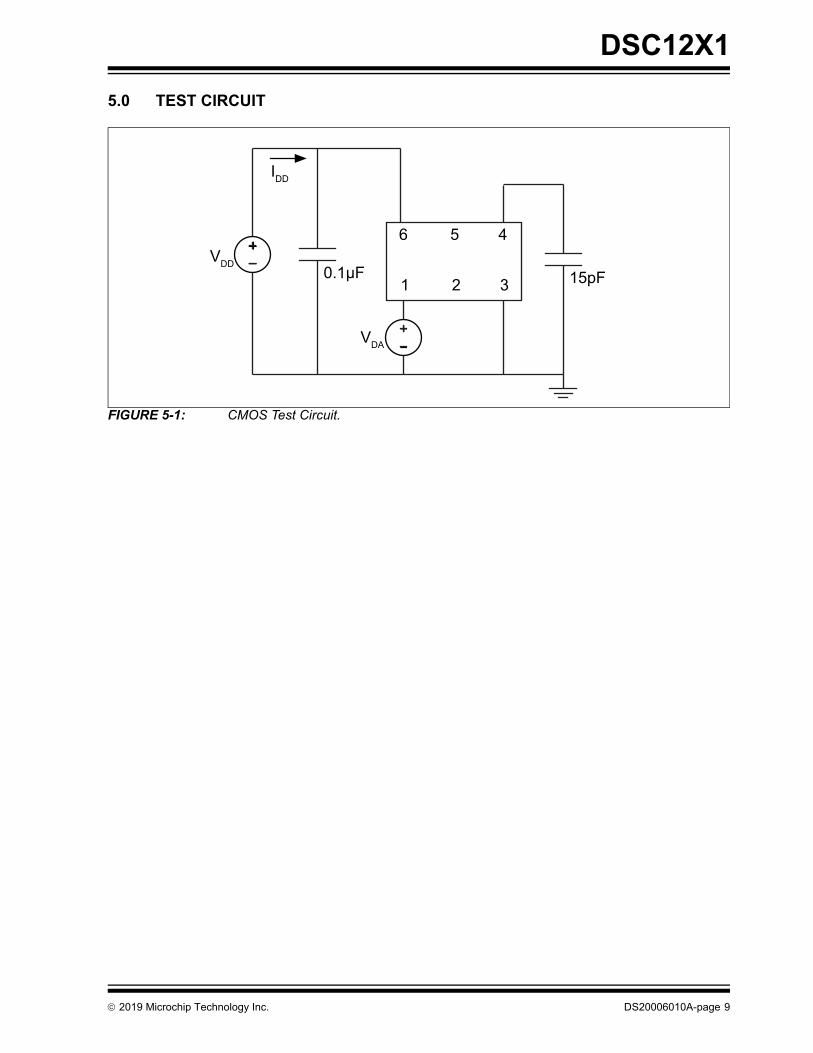
5.0 TEST CIRCUIT
FIGURE 5-1: CMOS Test Circuit.
6 5 4
1 2 30.1μF
VDD
VDA
IDD
15pF
DSC12X1
DS20006010A-page 10 2019 Microchip Technology Inc.
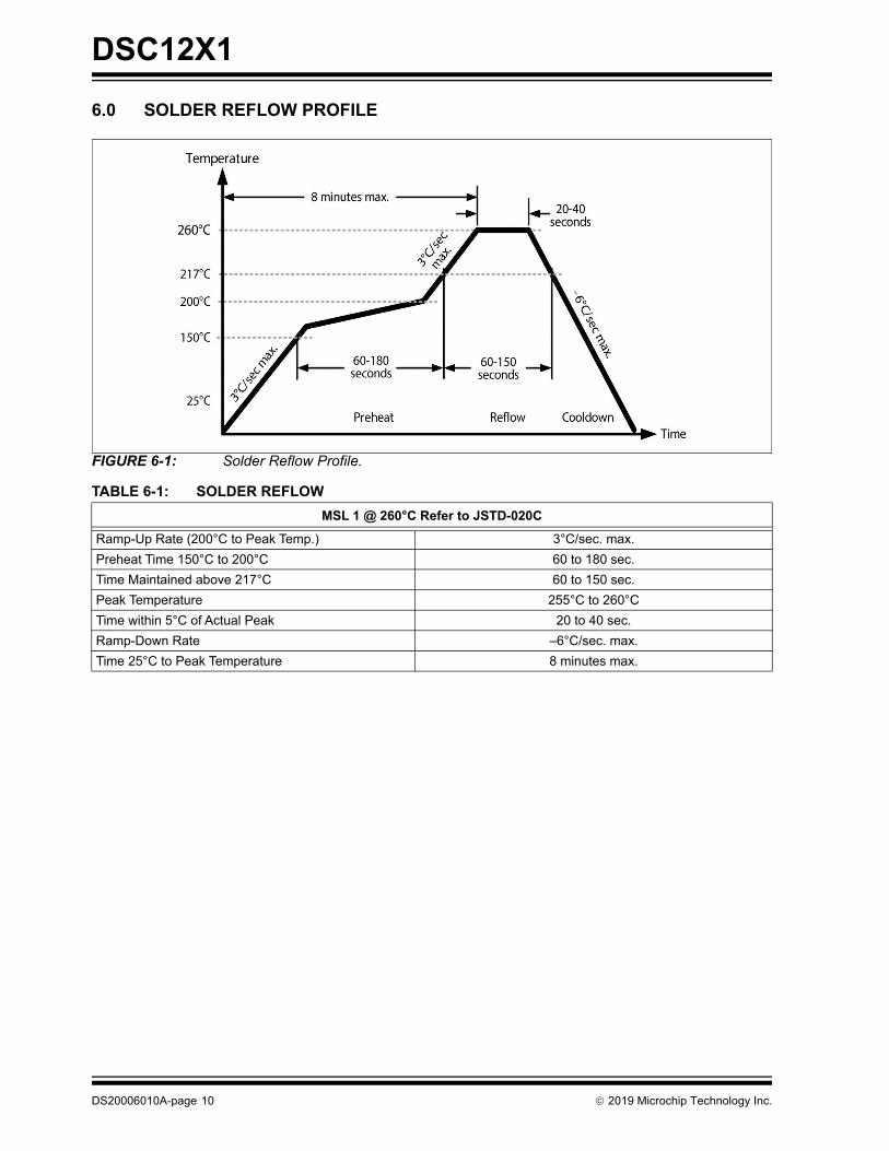
6.0 SOLDER REFLOW PROFILE
FIGURE 6-1: Solder Reflow Profile.
TABLE 6-1: SOLDER REFLOW
MSL 1 @ 260°C Refer to JSTD-020C
Ramp-Up Rate (200°C to Peak Temp.) 3°C/sec. max.
Preheat Time 150°C to 200°C 60 to 180 sec.
Time Maintained above 217°C 60 to 150 sec.
Peak Temperature 255°C to 260°C
Time within 5°C of Actual Peak 20 to 40 sec.
Ramp-Down Rate –6°C/sec. max.
Time 25°C to Peak Temperature 8 minutes max.
2019 Microchip Technology Inc. DS20006010A-page 11
DSC12X1
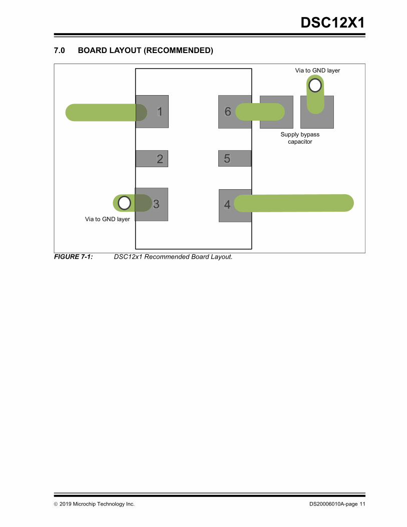
7.0 BOARD LAYOUT (RECOMMENDED)
FIGURE 7-1: DSC12x1 Recommended Board Layout.
1
3 4
6
52
4
52
3
61
Via to GND layer
Via to GND layer
Supply bypass capacitor

DSC12X1
DS20006010A-page 12 2019 Microchip Technology Inc.
8.0 PHASE NOISE
FIGURE 8-1: DSC12x1 Phase Noise at 25 MHz.
FIGURE 8-2: DSC12x1 Phase Noise at 125 MHz.

2019 Microchip Technology Inc. DS20006010A-page 13
DSC12X1
9.0 PACKAGING INFORMATION
9.1 Package Marking Information
Example6-Pin CDFN/VDFN*
XXXXXXXX
0SSSDCPYYWW
125M0000
0421DCP1723
Legend: XX...X Product code or customer-specific informationY Year code (last digit of calendar year)YY Year code (last 2 digits of calendar year)WW Week code (week of January 1 is week ‘01’)SSS Alphanumeric traceability code Pb-free JEDEC® designator for Matte Tin (Sn)* This package is Pb-free. The Pb-free JEDEC designator ( )
can be found on the outer packaging for this package.
, , Pin one index is identified by a dot, delta up, or delta down (trianglemark).
Note: In the event the full Microchip part number cannot be marked on one line, it willbe carried over to the next line, thus limiting the number of availablecharacters for customer-specific information. Package may or may not includethe corporate logo.
Underbar (_) and/or Overbar (⎯) symbol may not be to scale.
3e
3e
DSC12X1
DS20006010A-page 14 2019 Microchip Technology Inc.
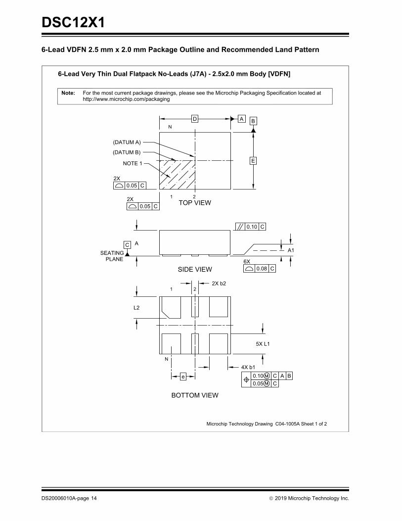
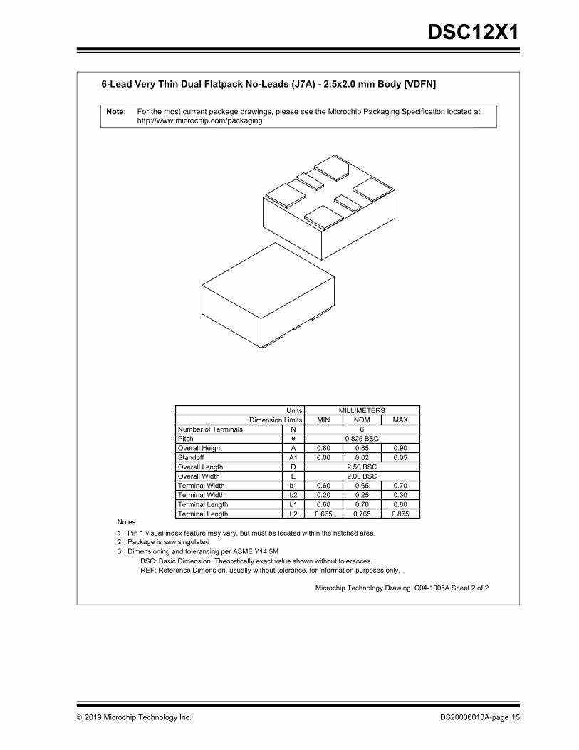
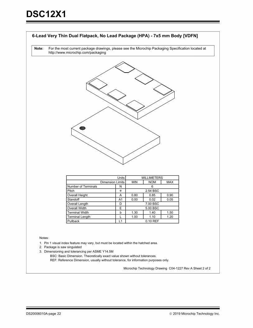
6-Lead VDFN 2.5 mm x 2.0 mm Package Outline and Recommended Land Pattern
BA
0.05 C
0.05 C
(DATUM B)
(DATUM A)
CSEATING
PLANE
1
N
2X TOP VIEW
SIDE VIEW
NOTE 1
0.10 C
0.08 C
Microchip Technology Drawing C04-1005A Sheet 1 of 2
2X
6X
For the most current package drawings, please see the Microchip Packaging Specification located athttp://www.microchip.com/packaging
Note:
6-Lead Very Thin Dual Flatpack No-Leads (J7A) - 2.5x2.0 mm Body [VDFN]
D
E
AA1
0.10 C A B0.05 C
BOTTOM VIEW
1 2
N
2X b2
4X b1
5X L1
L2
e
2
2019 Microchip Technology Inc. DS20006010A-page 15
DSC12X1
REF: Reference Dimension, usually without tolerance, for information purposes only.BSC: Basic Dimension. Theoretically exact value shown without tolerances.
1.2.3.
Notes:
Pin 1 visual index feature may vary, but must be located within the hatched area.Package is saw singulatedDimensioning and tolerancing per ASME Y14.5M
For the most current package drawings, please see the Microchip Packaging Specification located athttp://www.microchip.com/packaging
Note:
Microchip Technology Drawing C04-1005A Sheet 2 of 2
6-Lead Very Thin Dual Flatpack No-Leads (J7A) - 2.5x2.0 mm Body [VDFN]
Number of Terminals
Overall Height
Terminal WidthOverall Width
Terminal Length
Pitch
Standoff
UnitsDimension Limits
A1A
b1
e
L2
E
N0.825 BSC
0.665
0.60
0.800.00
0.65
0.765
0.850.02
2.00 BSC
MILLIMETERSMIN NOM
6
0.865
0.70
0.900.05
MAX
Overall Length D 2.50 BSC
Terminal Length L1 0.60 0.70 0.80Terminal Width b2 0.20 0.25 0.30
DSC12X1
DS20006010A-page 16 2019 Microchip Technology Inc.
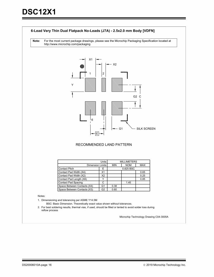
RECOMMENDED LAND PATTERN
Dimension LimitsUnits
C
Contact Pad Width (X4)
Contact Pad Spacing
Contact Pad Width (X2)
Contact Pitch
X2X1
0.250.65
MILLIMETERS
0.825 BSCMIN
EMAX
1.45
Space Between Contacts (X3)Space Between Contacts (X4)
G2G1
0.600.38
Microchip Technology Drawing C04-3005A
NOM
6-Lead Very Thin Dual Flatpack No-Leads (J7A) - 2.5x2.0 mm Body [VDFN]
1 2
6
YContact Pad Length (X6) 0.85
BSC: Basic Dimension. Theoretically exact value shown without tolerances.
Notes:Dimensioning and tolerancing per ASME Y14.5M
For best soldering results, thermal vias, if used, should be filled or tented to avoid solder loss duringreflow process
1.
2.
For the most current package drawings, please see the Microchip Packaging Specification located athttp://www.microchip.com/packaging
Note:
C
E
X1
X2
Y
G1
G2
SILK SCREEN
2019 Microchip Technology Inc. DS20006010A-page 17
DSC12X1
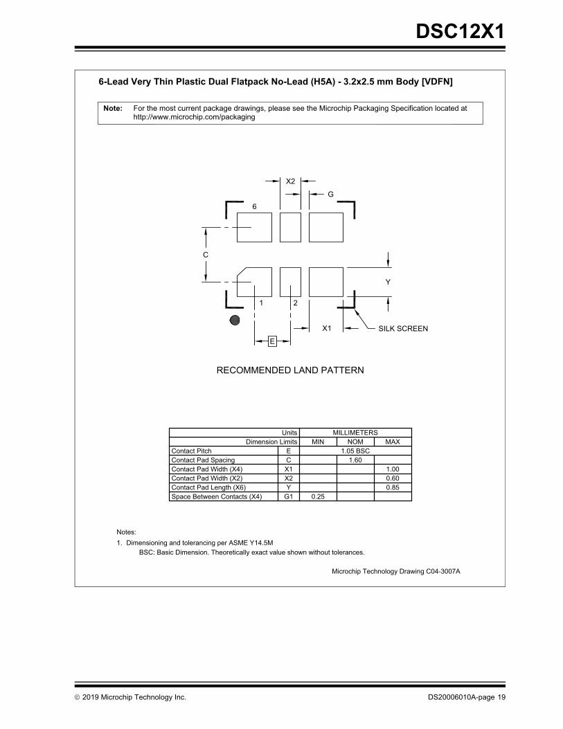
6-Lead VDFN 3.2 mm x 2.5 mm Package Outline and Recommended Land Pattern
BA
0.05 C
0.05 C
0.07 C A B0.05 C
(DATUM B)
(DATUM A)
CSEATING
PLANE
NOTE 1
1 2
N
2XTOP VIEW
SIDE VIEW
BOTTOM VIEW
NOTE 1
1 2
N
0.10 C
0.08 C
Microchip Technology Drawing C04-1007A Sheet 1 of 2
2X
6X
For the most current package drawings, please see the Microchip Packaging Specification located athttp://www.microchip.com/packaging
Note:
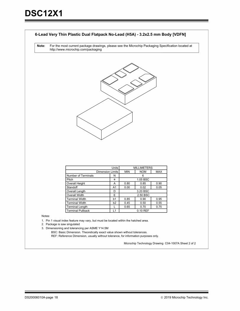
6-Lead Very Thin Plastic Dual Flatpack No-Lead (H5A) - 3.2x2.5 mm Body [VDFN]
D
E
e
2X b2
4X b1
L
L1
A
A1
DSC12X1
DS20006010A-page 18 2019 Microchip Technology Inc.
Microchip Technology Drawing C04-1007A Sheet 2 of 2
REF: Reference Dimension, usually without tolerance, for information purposes only.BSC: Basic Dimension. Theoretically exact value shown without tolerances.
1.2.3.
Notes:
Pin 1 visual index feature may vary, but must be located within the hatched area.Package is saw singulatedDimensioning and tolerancing per ASME Y14.5M
6-Lead Very Thin Plastic Dual Flatpack No-Lead (H5A) - 3.2x2.5 mm Body [VDFN]
For the most current package drawings, please see the Microchip Packaging Specification located athttp://www.microchip.com/packaging
Note:
Number of Terminals
Overall Height
Terminal Width
Overall Width
Terminal Length
Terminal Width
Pitch
Standoff
UnitsDimension Limits
A1A
b2b1
e
L
E
N1.05 BSC
0.85
0.650.45
0.800.00
0.500.70
0.90
0.850.02
2.50 BSC
MILLIMETERSMIN NOM
6
0.95
0.750.55
0.900.05
MAX
L1 0.10 REFTerminal Pullback
Overall Length D 3.20 BSC
2019 Microchip Technology Inc. DS20006010A-page 19
DSC12X1
RECOMMENDED LAND PATTERN
Dimension LimitsUnits
X1Contact Pad Width (X4)
Contact Pitch
MILLIMETERS
1.05 BSCMIN
EMAX
1.00
Contact Pad Length (X6)Contact Pad Width (X2)
YX2
0.85
Microchip Technology Drawing C04-3007A
NOM
6-Lead Very Thin Plastic Dual Flatpack No-Lead (H5A) - 3.2x2.5 mm Body [VDFN]
SILK SCREEN
1 2
6
CContact Pad Spacing 1.60
Space Between Contacts (X4) G1 0.25
BSC: Basic Dimension. Theoretically exact value shown without tolerances.
Notes:Dimensioning and tolerancing per ASME Y14.5M1.
For the most current package drawings, please see the Microchip Packaging Specification located athttp://www.microchip.com/packaging
Note:
C
E
X1
Y
X2
G
0.60
DSC12X1
DS20006010A-page 20 2019 Microchip Technology Inc.
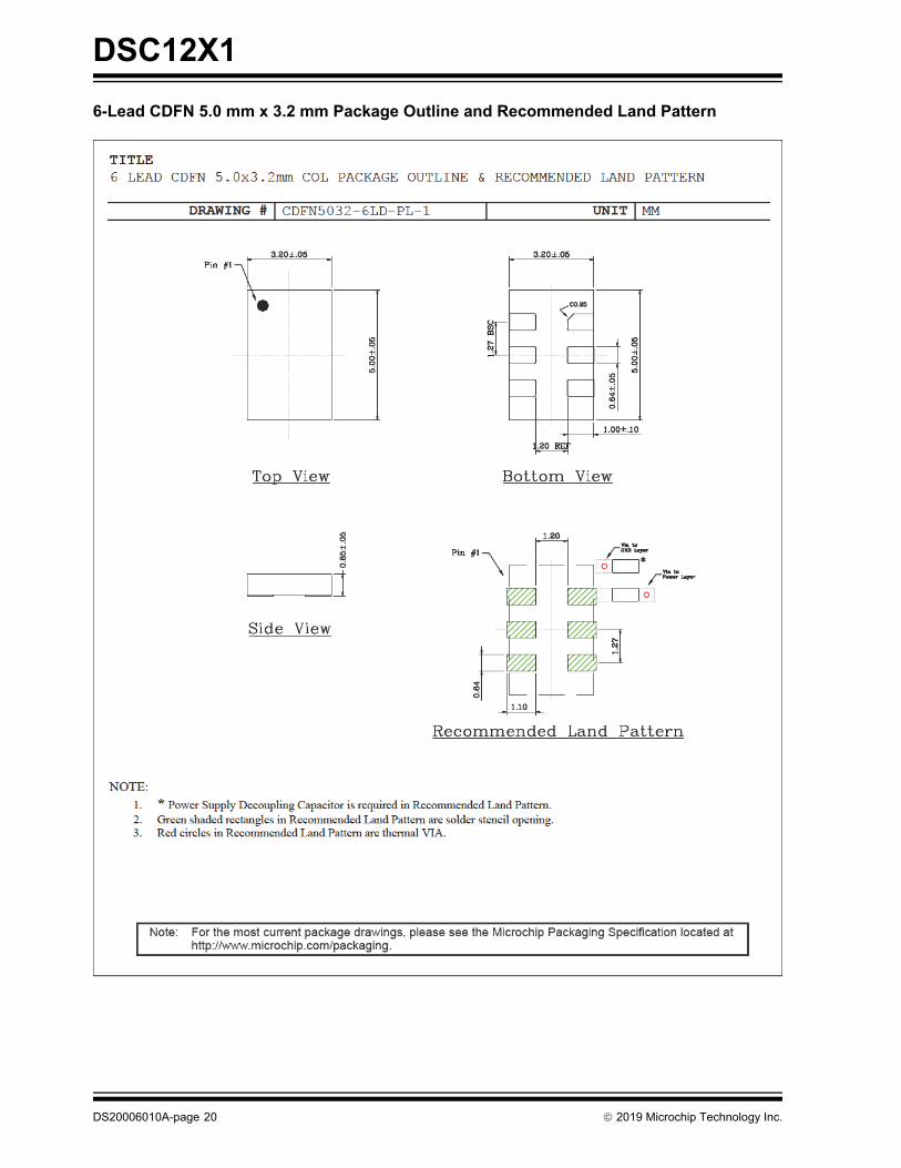
6-Lead CDFN 5.0 mm x 3.2 mm Package Outline and Recommended Land Pattern
2019 Microchip Technology Inc. DS20006010A-page 21
DSC12X1
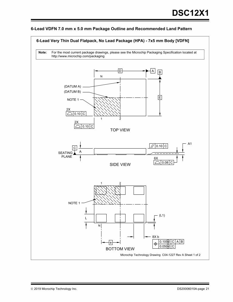
6-Lead VDFN 7.0 mm x 5.0 mm Package Outline and Recommended Land Pattern
DSC12X1
DS20006010A-page 22 2019 Microchip Technology Inc.
Notes:

2019 Microchip Technology Inc. DS20006010A-page 23
DSC12X1

DSC12X1
DS20006010A-page 24 2019 Microchip Technology Inc.
NOTES:

2019 Microchip Technology Inc. DS20006010A-page 25
DSC12X1
APPENDIX A: REVISION HISTORY
Revision A (April 2019)
• Initial release of DSC12x1 as Microchip data sheet DS20006010A.

DSC12X1
DS20006010A-page 26 2019 Microchip Technology Inc.
NOTES:

2019 Microchip Technology Inc. DS20006010A-page 27
DSC12X1
PRODUCT IDENTIFICATION SYSTEM
To order or obtain information, e.g., on pricing or delivery, contact your local Microchip representative or sales office.
Examples:
a) DSC1201NE1-25M00000T: Pin 1 STDBY with Pull-up, CMOS Output, 7x5 VDFN,–20°C to +70°C, ±50 ppm, 25 MHz Output Frequency, 1,000/Reel
b) DSC1211CL3-C0013: Pin 1 Frequency Selectwith Pull-up, CMOS Output, 3.2x2.5 VDFN,–40°C to +105°C, ±20 ppm, Frequency Select: 24 MHz & 25 MHz, Bulk
c) DSC1221BI2-19M5000000B: Pin 1 OE with Pull-up, CMOS Output, 5x3.2 CDFN, –40°C to +85°C, ±25 ppm, 19.5 MHz Output Frequency, 3,000/Reel
d) DSC1251DL3-55M82000T: Pin 2 OE with Pull-up, CMOS Output, 2.5x2 VDFN,–40°C to +105°C, ±20 ppm, 55.82 MHz Output Frequency, 1,000/Reel
e) DSC1231NI1-C0014B: Pin 2 STDBY with Pull-up, CMOS Output, 7x5 VDFN,–40°C to +85°C, ±50 ppm, Frequency Select:100 MHz & 156.25 MHz, 3,000/Reel
PART NO. X X
MediaPackageDevice
Device: DSC12: High Performance CMOS MEMS Oscillator
Control Pin: 0 = Pin 1 STDBY with Pull-up1 = Pin 1 Frequency Select with Pull-up (Note 1)2 = Pin 1 OE with Pull-up3 = Pin 2 STDBY with Pull-up4 = Pin 2 Frequency Select with Pull-up (Note 1)5 = Pin 2 OE with Pull-up
Output Format: 1 = CMOS
Package: N = 7 mm x 5 mm 6-Lead VDFN (Note 2)B = 5 mm x 3.2 mm 6-Lead CDFNC = 3.2 mm x 2.5 mm 6-Lead VDFND = 2.5 mm x 2 mm 6-Lead VDFN
Temperature: A = –40°C to +125°CL = –40°C to +105°CI = –40°C to +85°CE = –20°C to +70°C
Frequency Stability:
1 = ±50 ppm2 = ±25 ppm3 = ±20 ppm
Output Frequency: xMxxxxxx= <10 MHzxxMxxxxx= <100 MHzxxxMxxxx= >100 MHzCCCCC= with Frequency SelectPROG = TimeFlash
Media Type: <blank>= BulkT = 1,000/ReelB = 3,000/Reel
X
ControlPin
X
OutputType
Note 1: Tape and Reel identifier only appears in the catalog part number description. This identifier is used for ordering purposes and is not printed on the device package. Check with your Microchip Sales Office for package availability with the Tape and Reel option.
Format
X
Temperature
X
Freq. Stability
-XXXXXXXX
Output Frequency
Note 1: Please use the ClockWorks tool to select two frequencies andcreate the customized full part number.
2: With the N package option, only Pin 1 can be used for control(only allowable control pin options are 0, 1, or 2).
DSC12X1
DS20006010A-page 28 2019 Microchip Technology Inc.
NOTES:
2019 Microchip Technology Inc. DS20006010A-page 29
Information contained in this publication regarding deviceapplications and the like is provided only for your convenienceand may be superseded by updates. It is your responsibility toensure that your application meets with your specifications.MICROCHIP MAKES NO REPRESENTATIONS ORWARRANTIES OF ANY KIND WHETHER EXPRESS ORIMPLIED, WRITTEN OR ORAL, STATUTORY OROTHERWISE, RELATED TO THE INFORMATION,INCLUDING BUT NOT LIMITED TO ITS CONDITION,QUALITY, PERFORMANCE, MERCHANTABILITY ORFITNESS FOR PURPOSE. Microchip disclaims all liabilityarising from this information and its use. Use of Microchipdevices in life support and/or safety applications is entirely atthe buyer’s risk, and the buyer agrees to defend, indemnify andhold harmless Microchip from any and all damages, claims,suits, or expenses resulting from such use. No licenses areconveyed, implicitly or otherwise, under any Microchipintellectual property rights unless otherwise stated.
Trademarks
The Microchip name and logo, the Microchip logo, AnyRate, AVR, AVR logo, AVR Freaks, BitCloud, chipKIT, chipKIT logo, CryptoMemory, CryptoRF, dsPIC, FlashFlex, flexPWR, Heldo, JukeBlox, KeeLoq, Kleer, LANCheck, LINK MD, maXStylus, maXTouch, MediaLB, megaAVR, MOST, MOST logo, MPLAB, OptoLyzer, PIC, picoPower, PICSTART, PIC32 logo, Prochip Designer, QTouch, SAM-BA, SpyNIC, SST, SST Logo, SuperFlash, tinyAVR, UNI/O, and XMEGA are registered trademarks of Microchip Technology Incorporated in the U.S.A. and other countries.
ClockWorks, The Embedded Control Solutions Company, EtherSynch, Hyper Speed Control, HyperLight Load, IntelliMOS, mTouch, Precision Edge, and Quiet-Wire are registered trademarks of Microchip Technology Incorporated in the U.S.A.
Adjacent Key Suppression, AKS, Analog-for-the-Digital Age, Any Capacitor, AnyIn, AnyOut, BodyCom, CodeGuard, CryptoAuthentication, CryptoAutomotive, CryptoCompanion, CryptoController, dsPICDEM, dsPICDEM.net, Dynamic Average Matching, DAM, ECAN, EtherGREEN, In-Circuit Serial Programming, ICSP, INICnet, Inter-Chip Connectivity, JitterBlocker, KleerNet, KleerNet logo, memBrain, Mindi, MiWi, motorBench, MPASM, MPF, MPLAB Certified logo, MPLIB, MPLINK, MultiTRAK, NetDetach, Omniscient Code Generation, PICDEM, PICDEM.net, PICkit, PICtail, PowerSmart, PureSilicon, QMatrix, REAL ICE, Ripple Blocker, SAM-ICE, Serial Quad I/O, SMART-I.S., SQI, SuperSwitcher, SuperSwitcher II, Total Endurance, TSHARC, USBCheck, VariSense, ViewSpan, WiperLock, Wireless DNA, and ZENA are trademarks of Microchip Technology Incorporated in the U.S.A. and other countries.
SQTP is a service mark of Microchip Technology Incorporated in the U.S.A.
Silicon Storage Technology is a registered trademark of Microchip Technology Inc. in other countries.
GestIC is a registered trademark of Microchip Technology Germany II GmbH & Co. KG, a subsidiary of Microchip Technology Inc., in other countries.
All other trademarks mentioned herein are property of their respective companies.
© 2019, Microchip Technology Incorporated, All Rights Reserved.
ISBN: 978-1-5224-4350-6
Note the following details of the code protection feature on Microchip devices:
• Microchip products meet the specification contained in their particular Microchip Data Sheet.
• Microchip believes that its family of products is one of the most secure families of its kind on the market today, when used in the intended manner and under normal conditions.
• There are dishonest and possibly illegal methods used to breach the code protection feature. All of these methods, to our knowledge, require using the Microchip products in a manner outside the operating specifications contained in Microchip’s Data Sheets. Most likely, the person doing so is engaged in theft of intellectual property.
• Microchip is willing to work with the customer who is concerned about the integrity of their code.
• Neither Microchip nor any other semiconductor manufacturer can guarantee the security of their code. Code protection does not mean that we are guaranteeing the product as “unbreakable.”
Code protection is constantly evolving. We at Microchip are committed to continuously improving the code protection features of ourproducts. Attempts to break Microchip’s code protection feature may be a violation of the Digital Millennium Copyright Act. If such actsallow unauthorized access to your software or other copyrighted work, you may have a right to sue for relief under that Act.
Microchip received ISO/TS-16949:2009 certification for its worldwide headquarters, design and wafer fabrication facilities in Chandler and Tempe, Arizona; Gresham, Oregon and design centers in California and India. The Company’s quality system processes and procedures are for its PIC® MCUs and dsPIC® DSCs, KEELOQ® code hopping devices, Serial EEPROMs, microperipherals, nonvolatile memory and analog products. In addition, Microchip’s quality system for the design and manufacture of development systems is ISO 9001:2000 certified.
QUALITYMANAGEMENTSYSTEMCERTIFIEDBYDNV
== ISO/TS16949==
DS20006010A-page 30 2019 Microchip Technology Inc.
AMERICASCorporate Office2355 West Chandler Blvd.Chandler, AZ 85224-6199Tel: 480-792-7200 Fax: 480-792-7277Technical Support: http://www.microchip.com/supportWeb Address: www.microchip.com
AtlantaDuluth, GA Tel: 678-957-9614 Fax: 678-957-1455
Austin, TXTel: 512-257-3370
BostonWestborough, MA Tel: 774-760-0087 Fax: 774-760-0088
ChicagoItasca, IL Tel: 630-285-0071 Fax: 630-285-0075
DallasAddison, TX Tel: 972-818-7423 Fax: 972-818-2924
DetroitNovi, MI Tel: 248-848-4000
Houston, TX Tel: 281-894-5983
IndianapolisNoblesville, IN Tel: 317-773-8323Fax: 317-773-5453Tel: 317-536-2380
Los AngelesMission Viejo, CA Tel: 949-462-9523Fax: 949-462-9608Tel: 951-273-7800
Raleigh, NC Tel: 919-844-7510
New York, NY Tel: 631-435-6000
San Jose, CA Tel: 408-735-9110Tel: 408-436-4270
Canada - TorontoTel: 905-695-1980 Fax: 905-695-2078
ASIA/PACIFICAustralia - SydneyTel: 61-2-9868-6733
China - BeijingTel: 86-10-8569-7000
China - ChengduTel: 86-28-8665-5511
China - ChongqingTel: 86-23-8980-9588
China - DongguanTel: 86-769-8702-9880
China - GuangzhouTel: 86-20-8755-8029
China - HangzhouTel: 86-571-8792-8115
China - Hong Kong SARTel: 852-2943-5100
China - NanjingTel: 86-25-8473-2460
China - QingdaoTel: 86-532-8502-7355
China - ShanghaiTel: 86-21-3326-8000
China - ShenyangTel: 86-24-2334-2829
China - ShenzhenTel: 86-755-8864-2200
China - SuzhouTel: 86-186-6233-1526
China - WuhanTel: 86-27-5980-5300
China - XianTel: 86-29-8833-7252
China - XiamenTel: 86-592-2388138
China - ZhuhaiTel: 86-756-3210040
ASIA/PACIFICIndia - BangaloreTel: 91-80-3090-4444
India - New DelhiTel: 91-11-4160-8631
India - PuneTel: 91-20-4121-0141
Japan - OsakaTel: 81-6-6152-7160
Japan - TokyoTel: 81-3-6880- 3770
Korea - DaeguTel: 82-53-744-4301
Korea - SeoulTel: 82-2-554-7200
Malaysia - Kuala LumpurTel: 60-3-7651-7906
Malaysia - PenangTel: 60-4-227-8870
Philippines - ManilaTel: 63-2-634-9065
SingaporeTel: 65-6334-8870
Taiwan - Hsin ChuTel: 886-3-577-8366
Taiwan - KaohsiungTel: 886-7-213-7830
Taiwan - TaipeiTel: 886-2-2508-8600
Thailand - BangkokTel: 66-2-694-1351
Vietnam - Ho Chi MinhTel: 84-28-5448-2100
EUROPEAustria - WelsTel: 43-7242-2244-39Fax: 43-7242-2244-393
Denmark - CopenhagenTel: 45-4450-2828 Fax: 45-4485-2829
Finland - EspooTel: 358-9-4520-820
France - ParisTel: 33-1-69-53-63-20 Fax: 33-1-69-30-90-79
Germany - GarchingTel: 49-8931-9700
Germany - HaanTel: 49-2129-3766400
Germany - HeilbronnTel: 49-7131-67-3636
Germany - KarlsruheTel: 49-721-625370
Germany - MunichTel: 49-89-627-144-0 Fax: 49-89-627-144-44
Germany - RosenheimTel: 49-8031-354-560
Israel - Ra’anana Tel: 972-9-744-7705
Italy - Milan Tel: 39-0331-742611 Fax: 39-0331-466781
Italy - PadovaTel: 39-049-7625286
Netherlands - DrunenTel: 31-416-690399 Fax: 31-416-690340
Norway - TrondheimTel: 47-7288-4388
Poland - WarsawTel: 48-22-3325737
Romania - BucharestTel: 40-21-407-87-50
Spain - MadridTel: 34-91-708-08-90Fax: 34-91-708-08-91
Sweden - GothenbergTel: 46-31-704-60-40
Sweden - StockholmTel: 46-8-5090-4654
UK - WokinghamTel: 44-118-921-5800Fax: 44-118-921-5820
Worldwide Sales and Service
08/15/18