High-Performance, 16-bit Digital Signal...
324
© 2008 Microchip Technology Inc. Advance Information DS70318A dsPIC33FJ06GS101/X02 and dsPIC33FJ16GSX02/X04 Data Sheet High-Performance, 16-bit Digital Signal Controllers
Transcript of High-Performance, 16-bit Digital Signal...

© 2008 Microchip Technology Inc. Advance Information DS70318A
dsPIC33FJ06GS101/X02 anddsPIC33FJ16GSX02/X04
Data SheetHigh-Performance,
16-bit Digital Signal Controllers

dsPIC33FJ06GS101/X02 and dsPIC33FJ16GSX02/X04
Note the following details of the code protection feature on Microchip devices:• Microchip products meet the specification contained in their particular Microchip Data Sheet.
• Microchip believes that its family of products is one of the most secure families of its kind on the market today, when used in the intended manner and under normal conditions.
• There are dishonest and possibly illegal methods used to breach the code protection feature. All of these methods, to our knowledge, require using the Microchip products in a manner outside the operating specifications contained in Microchip’s Data Sheets. Most likely, the person doing so is engaged in theft of intellectual property.
• Microchip is willing to work with the customer who is concerned about the integrity of their code.
• Neither Microchip nor any other semiconductor manufacturer can guarantee the security of their code. Code protection does not mean that we are guaranteeing the product as “unbreakable.”
Code protection is constantly evolving. We at Microchip are committed to continuously improving the code protection features of ourproducts. Attempts to break Microchip’s code protection feature may be a violation of the Digital Millennium Copyright Act. If such actsallow unauthorized access to your software or other copyrighted work, you may have a right to sue for relief under that Act.
Information contained in this publication regarding deviceapplications and the like is provided only for your convenienceand may be superseded by updates. It is your responsibility toensure that your application meets with your specifications.MICROCHIP MAKES NO REPRESENTATIONS ORWARRANTIES OF ANY KIND WHETHER EXPRESS ORIMPLIED, WRITTEN OR ORAL, STATUTORY OROTHERWISE, RELATED TO THE INFORMATION,INCLUDING BUT NOT LIMITED TO ITS CONDITION,QUALITY, PERFORMANCE, MERCHANTABILITY ORFITNESS FOR PURPOSE. Microchip disclaims all liabilityarising from this information and its use. Use of Microchipdevices in life support and/or safety applications is entirely atthe buyer’s risk, and the buyer agrees to defend, indemnify andhold harmless Microchip from any and all damages, claims,suits, or expenses resulting from such use. No licenses areconveyed, implicitly or otherwise, under any Microchipintellectual property rights.
© 2008 Microchip Technology Inc.
Trademarks
The Microchip name and logo, the Microchip logo, Accuron, dsPIC, KEELOQ, KEELOQ logo, MPLAB, PIC, PICmicro, PICSTART, PRO MATE, rfPIC and SmartShunt are registered trademarks of Microchip Technology Incorporated in the U.S.A. and other countries.
FilterLab, Linear Active Thermistor, MXDEV, MXLAB, SEEVAL, SmartSensor and The Embedded Control Solutions Company are registered trademarks of Microchip Technology Incorporated in the U.S.A.
Analog-for-the-Digital Age, Application Maestro, CodeGuard, dsPICDEM, dsPICDEM.net, dsPICworks, dsSPEAK, ECAN, ECONOMONITOR, FanSense, In-Circuit Serial Programming, ICSP, ICEPIC, Mindi, MiWi, MPASM, MPLAB Certified logo, MPLIB, MPLINK, mTouch, PICkit, PICDEM, PICDEM.net, PICtail, PIC32 logo, PowerCal, PowerInfo, PowerMate, PowerTool, REAL ICE, rfLAB, Select Mode, Total Endurance, UNI/O, WiperLock and ZENA are trademarks of Microchip Technology Incorporated in the U.S.A. and other countries.
SQTP is a service mark of Microchip Technology Incorporated in the U.S.A.
All other trademarks mentioned herein are property of their respective companies.
© 2008, Microchip Technology Incorporated, Printed in the U.S.A., All Rights Reserved.
Printed on recycled paper.
DS70318A-page ii
Microchip received ISO/TS-16949:2002 certification for its worldwide headquarters, design and wafer fabrication facilities in Chandler and Tempe, Arizona; Gresham, Oregon and design centers in California and India. The Company’s quality system processes and procedures are for its PIC® MCUs and dsPIC® DSCs, KEELOQ® code hopping devices, Serial EEPROMs, microperipherals, nonvolatile memory and analog products. In addition, Microchip’s quality system for the design and manufacture of development systems is ISO 9001:2000 certified.

dsPIC33FJ06GS101/X02 anddsPIC33FJ16GSX02/X04
High-Performance, 16-bit Digital Signal Controllers
Operating Range:• Up to 40 MIPS operation (at 3.0-3.6V):
- Industrial temperature range (-40°C to +85°C)
- Extended temperature range (-40°C to +125°C)
High-Performance DSC CPU:• Modified Harvard architecture• C compiler optimized instruction set• 16-bit wide data path• 24-bit wide instructions• Linear program memory addressing up to 4M
instruction words• Linear data memory addressing up to 64 Kbytes• 83 base instructions: mostly 1 word/1 cycle• Two 40-bit accumulators with rounding and
saturation options• Flexible and powerful addressing modes:
- Indirect- Modulo- Bit-Reversed
• Software stack• 16 x 16 fractional/integer multiply operations• 32/16 and 16/16 divide operations• Single-cycle multiply and accumulate:
- Accumulator write back for DSP operations- Dual data fetch
• Up to ±16-bit shifts for up to 40-bit data
Digital I/O:• Peripheral pin Select functionality• Up to 35 programmable digital I/O pins• Wake-up/Interrupt-on-Change for up to 30 pins• Output pins can drive voltage from 3.0V to 3.6V• Up to 5V output with open drain configuration• 5V tolerant digital input pins (except RB5)• 16 mA source/sink on all PWM pins
On-Chip Flash and SRAM:• Flash program memory (up to 16 Kbytes)• Data SRAM (up to 2 Kbytes)• Boot and General Security for program Flash
Peripheral Features:• Timer/Counters, up to three 16-bit timers
- Can pair up to make one 32-bit timer• Input Capture (up to two channels):
- Capture on up, down or both edges- 16-bit capture input functions- 4-deep FIFO on each capture
• Output Compare (up to two channels):- Single or Dual 16-bit Compare mode- 16-bit Glitchless PWM mode
• 4-wire SPI:- Framing supports I/O interface to simple
codecs- 1-deep FIFO Buffer.- Supports 8-bit and 16-bit data- Supports all serial clock formats and
sampling modes• I2C™:
- Supports Full Multi-Master Slave mode - 7-bit and 10-bit addressing- Bus collision detection and arbitration- Integrated signal conditioning- Slave address masking
• UART:- Interrupt on address bit detect- Interrupt on UART error- Wake-up on Start bit from Sleep mode- 4-character TX and RX FIFO buffers- LIN bus support- IrDA© encoding and decoding in hardware- High-Speed Baud mode- Hardware Flow Control with CTS and RTS
Interrupt Controller:• 5-cycle latency• 118 interrupt vectors• Up to 35 available interrupt sources• Up to 3 external interrupts• Seven programmable priority levels• Four processor exceptions
© 2008 Microchip Technology Inc. DS70318A-page 1

dsPIC33FJ06GS101/X02 and dsPIC33FJ16GSX02/X04
High-Speed PWM Module Features:• Up to four PWM generators with 4-8 outputs• Individual time base and duty cycle for each of the
eight PWM outputs• Dead time for rising and falling edges:
- Duty cycle resolution of 1.04 ns- Dead-time resolution of 1.04 ns
• Phase shift resolution of 1.04 ns• Frequency resolution of 1.04 ns• PWM modes supported:
- Standard Edge-Aligned- True Independent Output- Complementary- Center-Aligned- Push-Pull- Multi-Phase- Variable Phase- Fixed Off-Time- Current Reset- Current-Limit
• Independent Fault/Current-Limit inputs for 8 PWM outputs
• Output override control• Special Event Trigger• PWM capture feature• Pre-scalar for input clock• Dual Trigger from PWM TO ADC• PWMxL, PWMxH output pin swapping• PWM4H, PWM4L pins remappable• On-the-Fly PWM Frequency, Duty cycle and
Phase Shift changes• Disabling of Individual PWM generators• Leading-Edge Blanking (LEB) functionality
High-Speed Analog Comparator• Up to four Analog Comparators:
- 20 ns response time- 10-bit DAC for each analog comparator- DACOUT pin to provide DAC output- Programmable output polarity- Selectable input source- ADC sample and convert capability
• PWM module interface:- PWM Duty Cycle Control- PWM Period Control- PWM Fault Detect
High-Speed 10-bit ADC• 10-bit resolution• Up to 12 input channels grouped into six
conversion pairs• Two internal reference monitoring inputs grouped
into a pair• Successive Approximation Register (SAR)
converters for parallel conversions of analog pairs:- 4 Msps for devices with two SARs- 2 Msps for devices with one SAR
• Dedicated result buffer for each analog channel• Independent trigger source section for each
analog input conversion pairs
Power Management:• On-chip 2.5V voltage regulator• Switch between clock sources in real time• Idle, Sleep, and Doze modes with fast wake-up
CMOS Flash Technology:• Low-power, high-speed Flash technology• Fully static design• 3.3V (±10%) operating voltage• Industrial and Extended temperature• Low power consumption
System Management:• Flexible clock options:
- External, crystal, resonator, internal RC- Phase-Locked Loop (PLL) with 120 MHz VCO- Primary Crystal Oscillator (OSC) in the range
of 3 MHz to 40 MHz- Internal Low-Power RC (LPRC) oscillator at a
frequency of 32 kHz- Internal Fast RC (FRC) oscillator at a
frequency of 7.37 MHz• Power-on Reset (POR)• Brown-out Reset (BOR)• Power-up Timer (PWRT) • Oscillator Start-up Timer (OST).• Watchdog Timer with its RC oscillator• Fail-Safe Clock Monitor• Reset by multiple sources• In-Circuit Serial Programming™ (ICSP™)
Packaging:• 18-pin SOIC• 28-pin SPDIP/SOIC/QFN-S• 44-pin TQFP/QFN
Note: See the device variant tables for exactperipheral features per device.
DS70318A-page 2 © 2008 Microchip Technology Inc.

dsPIC33FJ06GS101/X02 and dsPIC33FJ16GSX02/X04
IP
-S
IP
-S
IP
-S
P
IP
-S
P
dsPIC33FJ06GS101/X02 and dsPIC33FJ16GSX02/X04 PRODUCT FAMILIESThe device names, pin counts, memory sizes andperipheral availability of each device are listed below.The following pages show their pinout diagrams.
dsPIC33FJ06GS101/X02 and dsPIC33FJ16GSX02/X04 Controller Families
Device Pins
Prog
ram
Fla
sh M
emor
y (K
byte
s)
RA
M (B
ytes
)
Remappable Peripherals
DA
C O
utpu
t
I2 C™
ADC
I/O P
ins
Pack
ages
Rem
appa
ble
Pins
16-b
it Ti
mer
Inpu
t Cap
ture
Out
put C
ompa
re
UA
RT
SPI
PWM
(2)
Ana
log
Com
para
tor
Exte
rnal
Inte
rrup
ts(3
)
SAR
s
Sam
ple
and
Hol
d (S
&H
) Circ
uit
Ana
log-
to-D
igita
l Inp
uts
dsPIC33FJ06GS101 18 6 256 8 2 0 1 1 1 2x2(1) 0 3 0 1 1 3 6 13 SOIC
dsPIC33FJ06GS102 28 6 256 16 2 0 1 1 1 2x2 0 3 0 1 1 3 6 21 SPDSOIC
QFN
dsPIC33FJ06GS202 28 6 1K 16 2 1 1 1 1 2x2 2 3 1 1 1 3 6 21 SPDSOIC
QFN
dsPIC33FJ16GS402 28 16 2K 16 3 2 2 1 1 3x2 0 3 0 1 1 4 8 21 SPDSOIC
QFN
dsPIC33FJ16GS404 44 16 2K 30 3 2 2 1 1 3x2 0 3 0 1 1 4 8 35 QFNTQF
dsPIC33FJ16GS502 28 16 2K 16 3 2 2 1 1 4x2(1) 4 3 1 1 2 6 8 21 SPDSOIC
QFN
dsPIC33FJ16GS504 44 16 2K 30 3 2 2 1 1 4x2(1) 4 3 1 1 2 6 12 35 QFNTQF
Note 1: The PWM4H:PWM4L pins are remappable.2: The PWM fault pins and PWM synchronization pins are remappable.3: Only two out of three interrupts are remappable.
© 2008 Microchip Technology Inc. DS70318A-page 3

dsPIC33FJ06GS101/X02 and dsPIC33FJ16GSX02/X04
Pin Diagrams
18-Pin SOIC
28-Pin SOIC, SPDIPdsPIC
33FJ06GS101
MCLRAN0/RA0AN1/RA1
VDD
VSS
AN2/RA2
TDO/RP5/CN5/RB5(1) TMS/PGC2/EMUC2/RP4/CN4/RB4(1)TCK/PGD2/EMUD2/INT0/RP3/CN3/RB3(1)
VCAP/VDDCORE
OSCO/CLKO/AN7/RP2/CN2/RB2(1)OSCI/CLKI/AN6/RP1/CN1/RB1(1) VSS
PGC1/EMUC1/SDA1/RP7/CN7/RB7(1) PGD1/EMUD1/TDI/SCL1/RP6/CN6/RB6(1)
AN3/RP0/CN0/RB0(1)
1
2
345
678
9
18
17
161514
131211
10
PWM1L/RA3PWM1H/RA4
dsPIC33FJ06G
S102
MCLR
PWM1L/RA3PWM1H/RA4PWM2L/RP14/CN14/RB14(1)
PWM2H/RP13/CN13/RB13(1)
RP12/CN12/RB12(1)
RP11/CN11/RB11(1)VSS
VDD
AN0/RA0 AN1/RA1
AVDDAVSS
AN2/RA2
PGD3/EMUD3/RP8/CN8/RB8(1) PGC3/EMUC3/RP15/CN15/RB15(1)
TMS/PGC2/EMUC2/RP4/CN4/RB4(1)TCK/PGD2/EMUD2/INT0/RP3/CN3/RB3(1)
VDDCORE/VCAPOSCO/CLKO/RP2/CN2/RB2(1)OSCI/CLKIN/RP1/CN1/RB1(1)
VSS
TDO/RP5/CN5/RB5(1)
PGC1/EMUC1/SDA/RP7/CN7/RB7(1)
PGD1/EMUD1/TDI/SCL/RP6/CN6/RB6(1)
AN5/RP10/CN10/RB10(1)AN4/RP9/CN9/RB9(1)AN3/RP0/CN0/RB0(1)
1234567891011121314
2827262524232221201918171615
Note 1: The RP# pins can be used by any remappable peripheral. See the table “dsPIC33FJ06GS101/X02 anddsPIC33FJ16GSX02/X04 Controller Families” for the list of available peripherals
28-Pin SPDIP, SOIC
dsPIC33FJ06G
S202
MCLR
PWM1L/RA3PWM1H/RA4PWM2L/RP14/CN14/RB14(1)
PWM2H/RP13/CN13/RB13(1)
TCK/RP12/CN12/RB12(1)
TMS/RP11/CN11/RB11(1)VSS
VDD
AN0/CMP1A/RA0 AN1/CMP1B/RA1
AVDDAVSS
AN2/CMP1C/CMP2A/RA2
PGD3/EMUD3/RP8/CN8/RB8(1) PGC3/EMUC3/PGC3/EMUC3/RP15/CN15/RB15(1)
PGC2/EMUC2/EXTREF/RP4/CN4/RB4(1)PGD2/EMUD2/DACOUT/INT0/RP3/CN3/RB3(1)
VDDCORE/VCAPOSCO/CLKO/RP2/CN2/RB2(1)OSCI/CLKIN/RP1/CN1/RB1(1)
VSS
TDO/RP5CN5/RB5(1)
PGC1/EMUC1/SDA/RP7/CN7/RB7(1)
PGD1/EMUD1/TDI/SCL/RP6CN6/RB6(1)
AN5/CMP2D/RP10/CN10/RB10(1)AN4/CMP2C/RP9/CN9/RB9(1)
AN3/CMP1D/CMP2B/RP0/CN0/RB0(1)
1234567891011121314
2827262524232221201918171615
DS70318A-page 4 © 2008 Microchip Technology Inc.

dsPIC33FJ06GS101/X02 and dsPIC33FJ16GSX02/X04
Pin Diagrams (Continued)
28-Pin SPDIP, SOIC
28-Pin SPDIP, SOIC
dsPIC33FJ16G
S402
MCLR
PWM1L/RA3PWM1H/RA4PWM2L/RP14/CN14/RB14(1)
PWM2H/RP13/CN13/RB13(1)
TCK/PWM3L/RP12/CN12/RB12(1)
TMS/PWM3H/RP11/CN11/RB11(1)VSS
VDD
AN0/RA0AN1/RA1
AVDDAVSS
AN2/RA2
PGD3/EMUD3/RP8/CN8/RB8(1) PGC3/EMUC3/RP15/CN15/RB15(1)
PGC2/EMUC2/RP4/CN4/RB4(1)PGD2/EMUD2/INT0/RP3/CN3/RB3(1)
VDDCORE/VCAPOSCO/CLKO/AN7/RP2/CN2/RB2(1)OSCI/CLKIN/AN6/RP1/CN1/RB1(1)
VSS
TDO/RP5/CN5/RB5(1)
PGC1/EMUC1/SDA/RP7/CN7/RB7(1)
PGD1/EMUD1/TDI/SCL/RP6/CN6/RB6(1)
AN5/RP10/CN10/RB10(1)AN4/RP9/CN9/RB9(1)AN3/RP0/CN0/RB0(1)
1234567891011121314
2827262524232221201918171615
Note 1: The RP# pins can be used by any remappable peripheral. See the table “dsPIC33FJ06GS101/X02 anddsPIC33FJ16GSX02/X04 Controller Families” for the list of available peripherals
dsPIC33FJ16G
S502
MCLR
PWM1L/RA3PWM1H/RA4PWM2L/RP14/CN14/RB14(1)
PWM2H/RP13/CN13/RB13(1)
TCK/PWM3L/RP12/CN12/RB12(1)
TMS/PWM3H/RP11/CN11/RB11(1)VSS
VDD
AN0/CMP1A/RA0AN1/CMP1B/RA1
AVDDAVSS
AN2/CMP1C/CMP2A/RA2
CN8/RB8/PGD3/EMUD3/RP8/CN8/RB8(1) PGC3/EMUC3/RP15/CN15/RB15(1)
PGC2/EMUC2/EXTREF/PWM4L/RP4/CN4/RB4(1)PGD2/EMUD2/DACOUT/PWM4H/INT0/RP3/CN3/RB3(1)
VDDCORE/VCAPOSCO/CLKO/AN7/CMP3D/CMP4B/RP2/CN2/RB2(1)OSCI/CLKIN/AN6/CMP3C/CMP4A/RP1/CN1/RB1(1)
VSS
TDO/RP5/CN6/RB5(1)
PGC1/EMUC1/SDA/RP7/CN7/RB7(1)
PGD1/EMUD1/TDI/SCL/RP6/CN6/RB6(1)
AN5/CMP2D/CMP3B/RP10/CN10/RB0(1)AN4/CMP2C/CMP3A/RP9/CN9/RB9(1)AN3/CMP1D/CMP2B/RP0/CN0/RB0(1)
1234567891011121314
2827262524232221201918171615
© 2008 Microchip Technology Inc. DS70318A-page 5
dsPIC33FJ06GS101/X02 and dsPIC33FJ16GSX02/X04
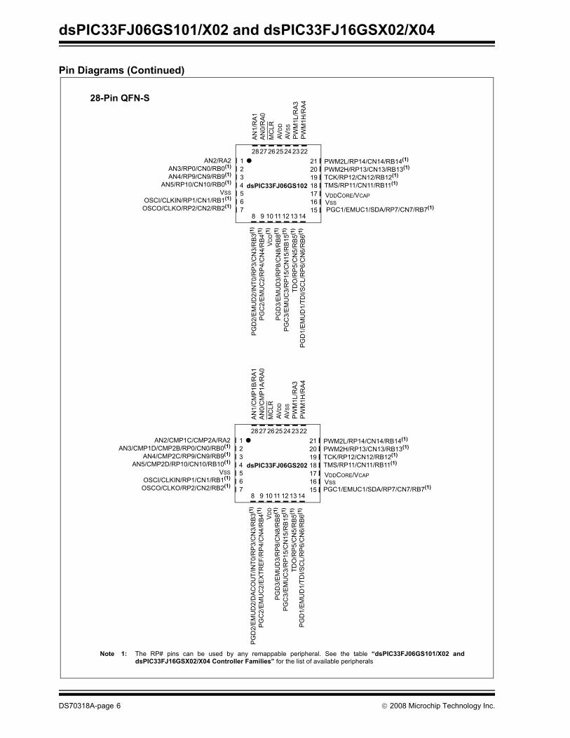
Pin Diagrams (Continued)
28-Pin QFN-S
10 11
23
6
1
18192021
22
12 13 1415
87
1617
232425262728
9
dsPIC33FJ06GS102
PGD
2/E
MU
D2/
INT0
/RP
3/C
N3/
RB
3(1)
54
AVD
DAV
SS
PW
M1L
/RA
3P
WM
1H/R
A4
PWM2L/RP14/CN14/RB14(1)
PWM2H/RP13/CN13/RB13(1)
TCK/RP12/CN12/RB12(1)
TMS/RP11/CN11/RB11(1)
VSSVDDCORE/VCAP
PGC1/EMUC1/SDA/RP7/CN7/RB7(1)
PGD
1/E
MU
D1/
TDI/S
CL/
RP
6/C
N6/
RB
6(1)
TDO
/RP
5/C
N5/
RB
5(1)
PG
C3/
EM
UC
3/R
P15/
CN
15/R
B15
(1)
MC
LRAN
0/R
A0AN
1/R
A1
AN2/RA2AN3/RP0/CN0/RB0(1)
AN4/RP9/CN9/RB9(1)
AN5/RP10/CN10/RB0(1)
VSSOSCI/CLKIN/RP1/CN1/RB1(1)
OSCO/CLKO/RP2/CN2/RB2(1)
PG
C2/
EM
UC
2/R
P4/
CN
4/R
B4(1
)
VD
D(1
)
PG
D3/
EM
UD
3/R
P8/
CN
8/R
B8(1
)
10 11
23
6
1
18192021
22
12 13 1415
87
1617
232425262728
9
dsPIC33FJ06GS202
PG
D2/
EMU
D2/
DA
CO
UT/
INT0
/RP
3/C
N3/
RB
3(1)
54
AVD
DAV
SS
PW
M1L
/RA3
PW
M1H
/RA
4
PWM2L/RP14/CN14/RB14(1)
PWM2H/RP13/CN13/RB13(1)
TCK/RP12/CN12/RB12(1)
TMS/RP11/CN11/RB11(1)
VSSVDDCORE/VCAP
PGC1/EMUC1/SDA/RP7/CN7/RB7(1)
PG
D1/
EMU
D1/
TDI/S
CL/
RP
6/C
N6/
RB
6(1)
TDO
/RP
5/C
N5/
RB
5(1)
PGC
3/E
MU
C3/
RP
15/C
N15
/RB
15(1
)
MC
LRA
N0/
CM
P1A
/RA
0A
N1/
CM
P1B
/RA
1
AN2/CMP1C/CMP2A/RA2AN3/CMP1D/CMP2B/RP0/CN0/RB0(1)
AN4/CMP2C/RP9/CN9/RB9(1)
AN5/CMP2D/RP10/CN10/RB10(1)
VSSOSCI/CLKIN/RP1/CN1/RB1(1)
OSCO/CLKO/RP2/CN2/RB2(1)
PGC
2/E
MU
C2/
EX
TRE
F/R
P4/
CN
4/R
B4(1
)
VD
DPG
D3/
EM
UD
3/R
P8/
CN
8/R
B8(1
)
Note 1: The RP# pins can be used by any remappable peripheral. See the table “dsPIC33FJ06GS101/X02 anddsPIC33FJ16GSX02/X04 Controller Families” for the list of available peripherals
DS70318A-page 6 © 2008 Microchip Technology Inc.

dsPIC33FJ06GS101/X02 and dsPIC33FJ16GSX02/X04
Pin Diagrams (Continued)
28-Pin QFN-S
10 11
23
6
1
18192021
22
12 13 1415
87
1617
232425262728
9
dsPIC33FJ16GS402
PG
D2/
EM
UD
2/IN
T0/R
P3/
CN
3/R
B3(1
)
54
AVD
DAV
SS
PW
M1L
/RA3
PW
M1H
/RA
4
PWM2L/RP14/CN14/RB14(1)
PWM2H/RP13/CN13/RB13(1)
TCK/PWM3L/RP12/CN12/RB12(1)
TMS/PWM3H/RP11/CN11/RB11(1)
VSSVDDCORE/VCAP
PGC1/EMUC1/SDA/RP7/CN7/RB7(1)
PG
D1/
EMU
D1/
TDI/S
CL/
RP
6/C
N6/
RB
6(1)
TDO
/RP
5/C
N5/
RB
5(1)
PGC
3/E
MU
C3/
RP
15/C
N15
/RB
15(1
)
MC
LRA
N0/
RA
0A
N1/
RA
1
AN2/RA2AN3/RP0/CN0/RB0(1)
AN4/RP9/CN9/RB9(1)
AN5/RP10/CN10/RB10(1)
VSSOSCI/CLKIN/AN6/RP1/CN1/RB1(1)
OSCO/CLKO/AN7/RP2/CN2/RB2(1)
PGC
2/E
MU
C2/
RP
4/C
N4/
RB
4(1)
VD
DPG
D3/
EM
UD
3/R
P8/
CN
8/R
B8(1
)
10 11
23
6
1
18192021
22
12 13 1415
87
1617
232425262728
9
dsPIC33FJ16GS502
PG
D2/
EM
UD
2/D
AC
OU
T/P
WM
4H/IN
T0/R
P3/
CN
3/R
B3(1
)
54
AVD
DAV
SS
PW
M1L
/RA
3P
WM
1H/R
A4
PWM2L/RP14/CN14/RB14(1)
PWM2H/RP13/CN13/RB13(1)
TCK/PWM3L/RP12/CN12/RB12(1)
TMS/PWM3H/RP11/CN11/RB11(1)
VSSVDDCORE/VCAP
PGC1/EMUC1/SDA/RP7/CN7/RB7(1)
PG
D1/
EM
UD
1/TD
I/SC
L/R
P6/
CN
6/R
B6(1
)TD
O/R
P5/
CN
5/R
B5(1
)PG
C3/
EM
UC
3/R
P15/
CN
15/R
B15
(1)
MC
LRAN
0/C
MP1
A/R
A0
AN1/
CM
P1B
/RA
1
AN2/CMP1C/CMP2A/RA2AN3/CMP1D/CMP2B/RP0/CN0/RB0(1)
AN4/CMP2C/CMP3A/RP9/CN9/RB9(1)
AN5/CMP2D/CMP3B/RP10/CN10/RB10(1)
VSSOSCI/CLKIN/AN6/CMP3C/CMP4A/RP1/CN1/RB1(1)
OSCO/CLKO/AN7/CMP3D/CMP4B/RP2/CN2/RB2(1)
PG
C2/
EMU
C2/
EXT
RE
F/PW
M4L
/RP
4/C
N4/
RB4
(1)
VDD
PGD
3/E
MU
D3/
RP
8/C
N8/
RB8
(1)
Note 1: The RP# pins can be used by any remappable peripheral. See the table “dsPIC33FJ06GS101/X02 anddsPIC33FJ16GSX02/X04 Controller Families” for the list of available peripherals
© 2008 Microchip Technology Inc. DS70318A-page 7

dsPIC33FJ06GS101/X02 and dsPIC33FJ16GSX02/X04
Pin Diagrams (Continued)
44-Pin QFN
44
dsPIC33FJ16GS404
43 42 41 40 39 38 37 36 35
12 13 14 15 16 17 18 19 20 21
33029282726252423
45
7891011
12 32
31
6
22
33
34
AN4/RP9/CN9/RB9(1)AN5/RP10/CN10/RB10(1)
OSCI/CLKI/AN6/RP1/CN1/RB1(1)OSCO/CLKO/AN7/RP2/CN2/RB2(1)
AN8/CMP4C/RP17/CN17/RC1(1)
RP26/CN26/RC10(1)VDD
RP25/CN25/RC9(1)
VSS
PG
D1/
EM
UD
1/TD
I/SC
L/R
P6/C
N6/
RB
6(1)
RP
18/C
N18
/RC
2(1)
PG
C3/
EM
UC
3/R
P15/
CN
15/R
B15
(1)
VD
D
PG
C2/
EM
UC
2/R
P4/C
N4/
RB
4(1)
RP
24/C
N24
/RC
8(1)
VS
S
TDO
/RP
5/C
N5/
RB5
(1)
PG
D3/
EM
UD
3/R
P8/C
N8/
RB
8(1)
RP
23/C
N23
/RC
7(1)
PG
D2/
EM
UD
2/IN
T0/R
P3/
CN
3/R
B3(1
)
PWM2H/RP13/CN13/RB13(1)TCK/PWM3L/RP12/CN12/RB12(1)TMS/PWM3H/RP11/CN11/RB11(1)
VDDCORE/VCAP
VSS
RP20/CN20/RC4(1)
RP19/CN19/RC3(1)RP22/CN22/RC6(1)RP21/CN21/RC5(1)
PGC1/EMUC1/SDA/RP7/CN7/RB7(1)
PWM2L/RP14/CN14/RB14(1)AN3/RP0/CN0/RB0(1)
AN2/RA2
AN
1/R
A1
AN
0/R
A0
MC
LR
RP
29/C
N29
/RC
13(1
)
AVD
D
AVS
S
PW
M1L
/RA3
PWM
1H/R
A4
RP1
6/C
N16
/RC
0(1)
RP
28/C
N28
/RC
12(1
) R
P27/
CN
27/R
C11
(1)
Note 1: The RP# pins can be used by any remappable peripheral. See the table “dsPIC33FJ06GS101/X02 anddsPIC33FJ16GSX02/X04 Controller Families” for the list of available peripherals
DS70318A-page 8 © 2008 Microchip Technology Inc.

dsPIC33FJ06GS101/X02 and dsPIC33FJ16GSX02/X04
Pin Diagrams (Continued)
44-Pin QFN
44
dsPIC33FJ16GS504
43 42 41 40 39 38 37 36 35
12 13 14 15 16 17 18 19 20 21
33029282726252423
45
789
1011
12 32
31
6
22
33
34
AN4/CMP2C/CMP3A/RP9/CN9/RB9(1)AN5/CMP2D/CMP3B/RP10/CN10/RB10(1)
OSCI/CLKI/AN6/CMP3C/CMP4A/RP1/CN1/RB1(1)OSCO/CLKO/AN7/CMP3D/CMP4B/RP2/CN2/RB2(1)
AN8/CMP4C/RP17/CN17/RC1(1)
AN10/RP26/CN26/RC10(1)VDD
AN11/RP25/CN25/RC9(1)
VSS
PG
D1/
EM
UD
1/TD
I/SC
L/R
P6/
CN
6/R
B6(1
)
AN
9/E
XTR
EF/
CM
P4D
/RP
18/C
N18
/RC
2(1)
PG
C3/
EM
UC
3/R
P15
/CN
15/R
B15
(1)
VD
D
PGC
2/E
MU
C2/
PW
M4L
/RP
4/C
N4/
RB
4(1)
RP
24/C
N24
/RC
8(1)
VS
S
TDO
/RP
5/C
N5/
RB
5(1)
PG
D3/
EM
UD
3/R
P8/
CN
8/R
B8(1
)
RP
23/C
N23
/RC
7(1)
PG
D2/
EMU
D2/
DAC
OU
T/PW
M4H
/INT0
/RP3
/CN
3/R
B3(1
)
PWM2H/RP13/CN13/RB13(1)TCK/PWM3L/RP12/CN12/RB12(1)TMS/PWM3H/RP11/CN11/RB11(1)
VDDCORE/VCAP
VSS
RP20/CN20/RC4(1)
RP19/CN19/RC3(1)RP22/RN22/RC6(1)RP21/CN21/RC5(1)
PGC1/EMUC1/SDA/RP7/CN7/RB7(1)
PWM2L/RP14/CN14/RB14(1)AN3/CMP1D/CMP2B/RP0/CN0/RB0(1)
AN2/CMP1C/CMP2A/RA2
AN
1/C
MP
1B/R
A1A
N0/
CM
P1A
/RA0
MC
LR
RP
29/C
N29
/RC
13(1
)
AVD
D
AVS
S
PW
M1L
/RA3
PWM
1H/R
A4
RP1
6/C
N16
/RC
0(1)
RP
28/C
N28
/RC
12(1
) R
P27
/CN
27/R
C11
(1)
Note 1: The RP# pins can be used by any remappable peripheral. See the table “dsPIC33FJ06GS101/X02 anddsPIC33FJ16GSX02/X04 Controller Families” for the list of available peripherals
© 2008 Microchip Technology Inc. DS70318A-page 9

dsPIC33FJ06GS101/X02 and dsPIC33FJ16GSX02/X04
Pin Diagrams (Continued)
44-Pin TQFP
1011
23456
1
18 19 20 21 2212 13 14 15
38
87
44 43 42 41 40 39
16 172930313233
232425262728
36 3435
9
37
PG
D1/
EM
UD
1/TD
I/SC
L/R
P6/
CN
6/R
B6(1
)
RP
18/C
N18
/RC
2(1)
PGC
3/E
MU
C3/
RP
15/C
N15
/RB
15(1
)
VD
D
PGC
2/E
MU
C2/
RP
4/C
N4/
RB4
(1)
RP
16/C
N16
/RC
0(1)
VS
S
TDO
/RP5
/CN
5/R
B5(1
)
PGD
3/E
MU
D3/
RP
8/C
N8/
RB8
(1)
RP2
3/C
N23
/RC
7(1)
AN3/RP0/CN0/RB0(1)
AN2/RA2
AN1/
RA1
AN0/
RA0
MC
LR
RP
29/C
N29
/RC
13(1
)
AVD
D
AVS
S
PW
M1L
/RA3
PWM
1H/R
A4
PWM2H/RP13/CN13/RB13(1)TCK/PWM3L/RP12/CN12/RB12(1)TMS/PWM3H/RP11/CN11/RB11(1)
VSS
VDDCORE/VCAP
RP19/CN19/RC3(1)RP22/CN22/RC6(1)RP21/CN21/RC5(1)
PGC1/EMUC1/SDA/RP7/CN7/RB7(1)
AN4/RP9/CN9/RB9(1)AN5/RP10/CN10/RB10(1)
OSCI/CLKI/AN6/RP1/CN1/RB1(1)OSCO/CLKO/AN7/RP2/CN2/RB2(1)
RP17/CN17/RC1(1)RP20/CN20/RC4(1)
VDD
VSS
RP
27/C
N27
/RC
11(1
)
RP
28/C
N28
/RC
12(1
)
PGD
2/E
MU
D2/
INT0
/RP
3/C
N3/
RB
3(1)
dsPIC33FJ16GS404
PWM2L/RP14/CN14/RB14(1)
RP2
4/C
N24
/RC
8(1)
RP25/CN25/RC9(1)RP26/CN26/RC10(1)
Note 1: The RP# pins can be used by any remappable peripheral. See the table “dsPIC33FJ06GS101/X02 anddsPIC33FJ16GSX02/X04 Controller Families” for the list of available peripherals
DS70318A-page 10 © 2008 Microchip Technology Inc.

dsPIC33FJ06GS101/X02 and dsPIC33FJ16GSX02/X04
Pin Diagrams (Continued)
44-Pin TQFP
1011
23456
118 19 20 21 2212 13 14 15
38
87
44 43 42 41 40 39
16 17
2930313233
232425262728
36 3435
9
37
PG
D1/
EMU
D1/
TDI/S
CL/
RP
6/C
N6/
RB
6(1)
AN
9/E
XTR
EF/
CM
P4D
/RP
18/C
N18
/RC
2(1)
PG
C3/
EMU
C3/
RP
15/C
N15
/RB1
5(1)
VD
D
PG
C2/
EM
UC
2/P
WM
4L/R
P4/C
N4/
RB
4(1)
RP1
6/C
N16
/RC
0(1)
VS
S
TDO
/RP
5/C
N5/
RB5
(1)
PG
D3/
EMU
D3/
RP
8/C
N8/
RB
8(1)
RP
23/C
N23
/RC
7(1)
AN3/CMP1D/CMP2B/RP0/CN0/RB0(1)
AN2/CMP1C/CMP2A/RA2
AN
1/C
MP
1B/R
A1A
N0/
CM
P1A
/RA0
MC
LR
RP
29/C
N29
/RC
13(1
)
AVD
D
AVS
S
PW
M1L
/RA3
PWM
1H/R
A4
PWM2H/RP13/CN13/RB13(1)TCK/PWM3L/RP12/CN12/RB12(1)TMS/PWM3H/RP11/CN11/RB11(1)
VSS
VDDCORE/VCAP
RP19/CN19/RC3(1)RP22/CN22/RC6(1)RP21/CN21/RC5(1)
PGC1/EMUC1/SDA/RP7/CN7/RB7(1)
AN4/CMP2C/CMP3A/RP9/CN9/RB9(1)AN5/CMP2D/CMP3B/RP10/CN10/RB10(1)
OSCI/CLKI/AN6/CMP3C/CMP4A/RP1/CN1/RB1(1)OSCO/CLKO/AN7/CMP3D/CMP4B/RP2/CN2/RB2(1)
AN8/CMP4C/RP17/CN17/RC1(1)RP20/CN20/RC4(1)
VDD
VSS
RP2
7/C
N27
/RC
11(1
)
RP
28/C
N28
/RC
12(1
)
PG
D2/
EMU
D2/
DA
CO
UT/
PW
M4H
/INT0
/RP
3/C
N3/
RB
3(1)
dsPIC33FJ16GS504
PWM2L/RP14/CN14/RB14(1)
RP
24/C
N24
/RC
8(1)
AN11/RP25/CN25/RC9(1)AN10/RP26/CN26/RC10(1)
Note 1: The RP# pins can be used by any remappable peripheral. See the table “dsPIC33FJ06GS101/X02 anddsPIC33FJ16GSX02/X04 Controller Families” for the list of available peripherals
© 2008 Microchip Technology Inc. DS70318A-page 11
dsPIC33FJ06GS101/X02 and dsPIC33FJ16GSX02/X04
Table of ContentsdsPIC33FJ06GS101/X02 and dsPIC33FJ16GSX02/X04 Product Families .......................................................................................... 31.0 Device Overview ........................................................................................................................................................................ 132.0 CPU............................................................................................................................................................................................ 173.0 Memory Organization ................................................................................................................................................................. 294.0 Flash Program Memory.............................................................................................................................................................. 695.0 Resets ....................................................................................................................................................................................... 756.0 Interrupt Controller ..................................................................................................................................................................... 837.0 Oscillator Configuration ......................................................................................................................................................... 1238.0 Power-Saving Features............................................................................................................................................................ 1339.0 I/O Ports .................................................................................................................................................................................. 13510.0 Timer1 ...................................................................................................................................................................................... 16511.0 Timer2/3 features .................................................................................................................................................................... 16712.0 Input Capture............................................................................................................................................................................ 17313.0 Output Compare....................................................................................................................................................................... 17514.0 High-Speed PWM..................................................................................................................................................................... 17915.0 Serial Peripheral Interface (SPI)............................................................................................................................................... 20116.0 Inter-Integrated Circuit (I2C™) ................................................................................................................................................. 20917.0 Universal Asynchronous Receiver Transmitter (UART) ........................................................................................................... 21918.0 High-Speed 10-bit Analog-to-Digital Converter (ADC) ............................................................................................................. 22719.0 High-Speed Analog Comparator .............................................................................................................................................. 24720.0 Special Features ...................................................................................................................................................................... 25121.0 Instruction Set Summary .......................................................................................................................................................... 25922.0 Development Support............................................................................................................................................................... 26723.0 Electrical Characteristics .......................................................................................................................................................... 27124.0 Packaging Information.............................................................................................................................................................. 303Appendix A: Revision History............................................................................................................................................................. 313Index ................................................................................................................................................................................................. 315The Microchip Web Site ..................................................................................................................................................................... 319Customer Change Notification Service .............................................................................................................................................. 319Customer Support .............................................................................................................................................................................. 319Reader Response .............................................................................................................................................................................. 320Product Identification System............................................................................................................................................................. 321
TO OUR VALUED CUSTOMERSIt is our intention to provide our valued customers with the best documentation possible to ensure successful use of your Microchipproducts. To this end, we will continue to improve our publications to better suit your needs. Our publications will be refined andenhanced as new volumes and updates are introduced. If you have any questions or comments regarding this publication, please contact the Marketing Communications Department viaE-mail at [email protected] or fax the Reader Response Form in the back of this data sheet to (480) 792-4150. Wewelcome your feedback.
Most Current Data SheetTo obtain the most up-to-date version of this data sheet, please register at our Worldwide Web site at:
http://www.microchip.comYou can determine the version of a data sheet by examining its literature number found on the bottom outside corner of any page.The last character of the literature number is the version number, (e.g., DS30000A is version A of document DS30000).
ErrataAn errata sheet, describing minor operational differences from the data sheet and recommended workarounds, may exist for currentdevices. As device/documentation issues become known to us, we will publish an errata sheet. The errata will specify the revisionof silicon and revision of document to which it applies.To determine if an errata sheet exists for a particular device, please check with one of the following:• Microchip’s Worldwide Web site; http://www.microchip.com• Your local Microchip sales office (see last page)When contacting a sales office, please specify which device, revision of silicon and data sheet (include literature number) you areusing.
Customer Notification SystemRegister on our web site at www.microchip.com to receive the most current information on all of our products.
DS70318A-page 12 © 2008 Microchip Technology Inc.

dsPIC33FJ06GS101/X02 and dsPIC33FJ16GSX02/X04
1.0 DEVICE OVERVIEW
This document contains device-specific information forthe following dsPIC33F Digital Signal Controller (DSC)devices:
• dsPIC33FJ06GS101• dsPIC33FJ06GS102• dsPIC33FJ06GS202• dsPIC33FJ16GS402• dsPIC33FJ16GS404• dsPIC33FJ16GS502• dsPIC33FJ16GS504
dsPIC33FJ06GS101/X02 and dsPIC33FJ16GSX02/X04 devices contain extensive Digital Signal Processor(DSP) functionality with a high-performance 16-bitmicrocontroller (MCU) architecture.
Figure 1-1 shows a general block diagram of the coreand peripheral modules in the dsPIC33FJ06GS101/X02and dsPIC33FJ16GSX02/X04 devices. Table 1-1 liststhe functions of the various pins shown in the pinoutdiagrams.
Note: This data sheet summarizes the featuresof the dsPIC33FJ06GS101/X02 anddsPIC33FJ16GSX02/X04 families ofdevices. It is not intended to be acomprehensive reference source. Tocomplement the information in this datasheet, refer to the “dsPIC33F FamilyReference Manual”. Please see theMicrochip web site (www.microchip.com)for the latest dsPIC33F Family ReferenceManual sections.
© 2008 Microchip Technology Inc. DS70318A-page 13

dsPIC33FJ06GS101/X02 and dsPIC33FJ16GSX02/X04
FIGURE 1-1: dsPIC33FJ06GS101/X02 and dsPIC33FJ16GSX02/X04 BLOCK DIAGRAM
16
OSC1/CLKIOSC2/CLKO
VDD, VSS
TimingGeneration
MCLR
Power-upTimer
OscillatorStart-up Timer
Power-onReset
WatchdogTimer
Brown-outReset
Precision
ReferenceBand Gap
FRC/LPRCOscillators
RegulatorVoltage
VDDCORE/VCAP
IC1,2 I2C1
PORTA
InstructionDecode &
Control
PCH PCL
16
Program Counter
16-bit ALU
23
23
24
23
Instruction Reg
PCU
16 x 16W Register Array
ROM Latch
16
EA MUX
16
16
8
InterruptController
PSV & TableData AccessControl Block
StackControl Logic
LoopControlLogic
Data Latch
AddressLatch
Address Latch
Program Memory
Data LatchAddress Bus
L
itera
l Dat
a 16 16
16
16
Data Latch
AddressLatch
16
X RAM Y RAM
16
Y Data Bus
X Data Bus
DSP Engine
Divide Support
16
Control Signals to Various Blocks
ADC1Timers
PORTB
Address Generator Units
1-3
CNx
UART1PWM
4 x 2
RemappablePins
PORTC
SPI1
OC1OC2
AnalogComparator 1-4
Note: Not all pins or features are implemented on all device pinout configurations. See pinout diagrams for the specific pins and featurespresent on each device.
DS70318A-page 14 © 2008 Microchip Technology Inc.
dsPIC33FJ06GS101/X02 and dsPIC33FJ16GSX02/X04
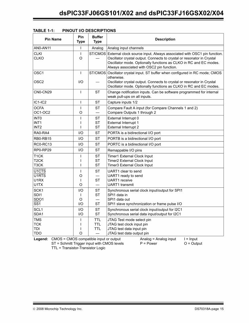
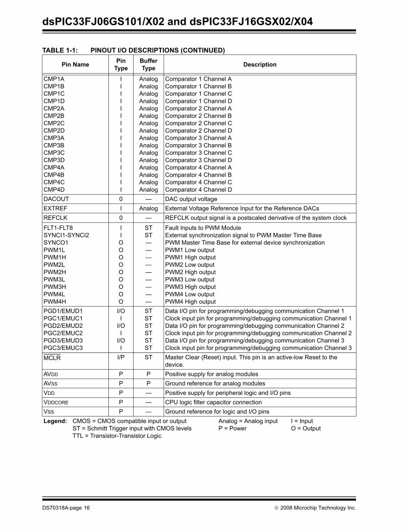
TABLE 1-1: PINOUT I/O DESCRIPTIONS
Pin Name PinType
BufferType Description
AN0-AN11 I Analog Analog input channelsCLKICLKO
IO
ST/CMOS—
External clock source input. Always associated with OSC1 pin function.Oscillator crystal output. Connects to crystal or resonator in Crystal Oscillator mode. Optionally functions as CLKO in RC and EC modes. Always associated with OSC2 pin function.
OSC1
OSC2
I
I/O
ST/CMOS
—
Oscillator crystal input. ST buffer when configured in RC mode; CMOS otherwise.Oscillator crystal output. Connects to crystal or resonator in Crystal Oscillator mode. Optionally functions as CLKO in RC and EC modes.
CN0-CN29 I ST Change notification inputs. Can be software programmed for internal weak pull-ups on all inputs.
IC1-IC2 I ST Capture inputs 1/2OCFAOC1-OC2
IO
ST—
Compare Fault A input (for Compare Channels 1 and 2)Compare Outputs 1 through 2
INT0INT1INT2
III
STSTST
External Interrupt 0External Interrupt 1External Interrupt 2
RA0-RA4 I/O ST PORTA is a bidirectional I/O portRB0-RB15 I/O ST PORTB is a bidirectional I/O portRC0-RC13 I/O ST PORTC is a bidirectional I/O portRP0-RP29 I/O ST Remappable I/O pinsT1CKT2CKT3CK
III
STSTST
Timer1 External Clock InputTimer2 External Clock InputTimer3 External Clock Input
U1CTSU1RTSU1RXU1TX
IOIO
ST—ST—
UART1 clear to sendUART1 ready to sendUART1 receiveUART1 transmit
SCK1SDI1SDO1SS1
I/OIOI/O
STST—ST
Synchronous serial clock input/output for SPI1SPI1 data inSPI1 data outSPI1 slave synchronization or frame pulse I/O
SCL1SDA1
I/OI/O
STST
Synchronous serial clock input/output for I2C1Synchronous serial data input/output for I2C1
TMSTCKTDITDO
IIIO
TTLTTLTTL—
JTAG Test mode select pinJTAG test clock input pinJTAG test data input pinJTAG test data output pin
Legend: CMOS = CMOS compatible input or output Analog = Analog input I = InputST = Schmitt Trigger input with CMOS levels P = Power O = OutputTTL = Transistor-Transistor Logic
© 2008 Microchip Technology Inc. DS70318A-page 15
dsPIC33FJ06GS101/X02 and dsPIC33FJ16GSX02/X04
CMP1ACMP1BCMP1CCMP1DCMP2ACMP2BCMP2CCMP2DCMP3ACMP3BCMP3CCMP3DCMP4ACMP4BCMP4CCMP4D
IIIIIIIIIIIIIIII
AnalogAnalogAnalogAnalogAnalogAnalogAnalogAnalogAnalogAnalogAnalogAnalogAnalogAnalogAnalogAnalog
Comparator 1 Channel AComparator 1 Channel BComparator 1 Channel CComparator 1 Channel DComparator 2 Channel AComparator 2 Channel BComparator 2 Channel CComparator 2 Channel DComparator 3 Channel AComparator 3 Channel BComparator 3 Channel CComparator 3 Channel DComparator 4 Channel AComparator 4 Channel BComparator 4 Channel CComparator 4 Channel D
DACOUT 0 — DAC output voltageEXTREF I Analog External Voltage Reference Input for the Reference DACsREFCLK 0 — REFCLK output signal is a postscaled derivative of the system clock
FLT1-FLT8SYNCI1-SYNCI2SYNCO1PWM1LPWM1HPWM2LPWM2HPWM3LPWM3HPWM4LPWM4H
IIOOOOOOOOO
STST—————————
Fault Inputs to PWM ModuleExternal synchronization signal to PWM Master Time BasePWM Master Time Base for external device synchronizationPWM1 Low outputPWM1 High outputPWM2 Low outputPWM2 High outputPWM3 Low outputPWM3 High outputPWM4 Low outputPWM4 High output
PGD1/EMUD1PGC1/EMUC1PGD2/EMUD2PGC2/EMUC2PGD3/EMUD3PGC3/EMUC3
I/OI
I/OI
I/OI
STSTSTSTSTST
Data I/O pin for programming/debugging communication Channel 1Clock input pin for programming/debugging communication Channel 1Data I/O pin for programming/debugging communication Channel 2Clock input pin for programming/debugging communication Channel 2Data I/O pin for programming/debugging communication Channel 3Clock input pin for programming/debugging communication Channel 3
MCLR I/P ST Master Clear (Reset) input. This pin is an active-low Reset to the device.
AVDD P P Positive supply for analog modulesAVSS P P Ground reference for analog modulesVDD P — Positive supply for peripheral logic and I/O pinsVDDCORE P — CPU logic filter capacitor connectionVSS P — Ground reference for logic and I/O pins
TABLE 1-1: PINOUT I/O DESCRIPTIONS (CONTINUED)
Pin Name PinType
BufferType Description
Legend: CMOS = CMOS compatible input or output Analog = Analog input I = InputST = Schmitt Trigger input with CMOS levels P = Power O = OutputTTL = Transistor-Transistor Logic
DS70318A-page 16 © 2008 Microchip Technology Inc.

dsPIC33FJ06GS101/X02 and dsPIC33FJ16GSX02/X04
2.0 CPU
The dsPIC33FJ06GS101/X02 anddsPIC33FJ16GSX02/X04 CPU module has a 16-bit(data) modified Harvard architecture with an enhancedinstruction set, including significant support for DSP. TheCPU has a 24-bit instruction word with a variable lengthopcode field. The Program Counter (PC) is 23 bits wideand addresses up to 4M x 24 bits of user program mem-ory space. The actual amount of program memory imple-mented varies from device to device. A single-cycleinstruction prefetch mechanism is used to help maintainthroughput and provides predictable execution. Allinstructions execute in a single cycle, with the exceptionof instructions that change the program flow, the dou-ble-word move (MOV.D) instruction and the table instruc-tions. Overhead-free program loop constructs aresupported using the DO and REPEAT instructions, both ofwhich are interruptible at any point.
The dsPIC33FJ06GS101/X02 anddsPIC33FJ16GSX02/X04 devices have sixteen, 16-bitworking registers in the programmer’s model. Each of theworking registers can serve as a data, address or addressoffset register. The sixteenth working register (W15) oper-ates as a software Stack Pointer (SP) for interrupts andcalls.
There are two classes of instruction in thedsPIC33FJ06GS101/X02 anddsPIC33FJ16GSX02/X04 devices: MCU and DSP.These two instruction classes are seamlesslyintegrated into a single CPU. The instruction setincludes many addressing modes and is designed foroptimum C compiler efficiency. For most instructions,the dsPIC33FJ06GS101/X02 anddsPIC33FJ16GSX02/X04 is capable of executing adata (or program data) memory read, a workingregister (data) read, a data memory write and aprogram (instruction) memory read per instructioncycle. As a result, three parameter instructions can besupported, allowing A + B = C operations to beexecuted in a single cycle.
A block diagram of the CPU is shown in Figure 2-1, andthe programmer’s model for thedsPIC33FJ06GS101/X02 anddsPIC33FJ16GSX02/X04 is shown in Figure 2-2.
2.1 Data Addressing OverviewThe data space can be addressed as 32K words or64 Kbytes and is split into two blocks, referred to as Xand Y data memory. Each memory block has its ownindependent Address Generation Unit (AGU). TheMCU class of instructions operates solely throughthe X memory AGU, which accesses the entirememory map as one linear data space. Certain DSPinstructions operate through the X and Y AGUs tosupport dual operand reads, which splits the dataaddress space into two parts. The X and Y data spaceboundary is device-specific.
Overhead-free circular buffers (Modulo Addressingmode) are supported in both X and Y address spaces.The Modulo Addressing removes the softwareboundary checking overhead for DSP algorithms.Furthermore, the X AGU circular addressing can beused with any of the MCU class of instructions. The XAGU also supports Bit-Reversed Addressing to greatlysimplify input or output data reordering for radix-2 FFTalgorithms.
The upper 32 Kbytes of the data space memory mapcan optionally be mapped into program space at any16K program word boundary defined by the 8-bitProgram Space Visibility Page (PSVPAG) register. Theprogram-to-data-space mapping feature lets anyinstruction access program space as if it were dataspace.
2.2 DSP Engine OverviewThe DSP engine features a high-speed 17-bit by 17-bitmultiplier, a 40-bit ALU, two 40-bit saturatingaccumulators and a 40-bit bidirectional barrel shifter.The barrel shifter is capable of shifting a 40-bit value upto 16 bits right or left, in a single cycle. The DSPinstructions operate seamlessly with all otherinstructions and have been designed for optimalreal-time performance. The MAC instruction and otherassociated instructions can concurrently fetch two dataoperands from memory while multiplying two Wregisters and accumulating and optionally saturatingthe result in the same cycle. This instructionfunctionality requires that the RAM data space be splitfor these instructions and linear for all others. Dataspace partitioning is achieved in a transparent andflexible manner through dedicating certain workingregisters to each address space.
Note: This data sheet summarizes the featuresof the dsPIC33FJ06GS101/X02 anddsPIC33FJ16GSX02/X04 families ofdevices. It is not intended to be acomprehensive reference source. Tocomplement the information in this datasheet, refer to the dsPIC33F Family Refer-ence Manual, “Section 2. CPU”(DS70204), which is available from theMicrochip website (www.microchip.com).
© 2008 Microchip Technology Inc. Advance Information DS70318A-page 17

dsPIC33FJ06GS101/X02 and dsPIC33FJ16GSX02/X04
2.3 Special MCU FeaturesThe dsPIC33FJ06GS101/X02 anddsPIC33FJ16GSX02/X04 features a 17-bit by 17-bitsingle-cycle multiplier that is shared by both the MCUALU and DSP engine. The multiplier can performsigned, unsigned and mixed-sign multiplication. Usinga 17-bit by 17-bit multiplier for 16-bit by 16-bitmultiplication not only allows you to perform mixed-signmultiplication, it also achieves accurate results forspecial operations, such as (-1.0) x (-1.0).
The dsPIC33FJ06GS101/X02 anddsPIC33FJ16GSX02/X04 supports 16/16 and 32/16divide operations, both fractional and integer. All divideinstructions are iterative operations. They must beexecuted within a REPEAT loop, resulting in a totalexecution time of 19 instruction cycles. The divideoperation can be interrupted during any of those19 cycles without loss of data.
A 40-bit barrel shifter is used to perform up to a 16-bitleft or right shift in a single cycle. The barrel shifter canbe used by both MCU and DSP instructions.
FIGURE 2-1: dsPIC33FJ06GS101/X02 and dsPIC33FJ16GSX02/X04 CPU CORE BLOCK DIAGRAM
InstructionDecode &
Control
PCH PCLProgram Counter
16-bit ALU
24
23
Instruction Reg
PCU
16 x 16W Register Array
ROM Latch
EA MUX
InterruptController
StackControlLogic
LoopControlLogic
Data Latch
AddressLatch
Control Signalsto Various Blocks
Address Bus
L
itera
l Dat
a
16 16
16
To Peripheral Modules
Data Latch
AddressLatch
16
X RAM Y RAM
Address Generator Units
16
Y Data Bus
X Data Bus
DSP Engine
Divide Support
16
16
23
23
168
PSV & TableData AccessControl Block
16
16
16
16
Program Memory
Data Latch
Address Latch
DS70318A-page 18 Advance Information © 2008 Microchip Technology Inc.

dsPIC33FJ06GS101/X02 and dsPIC33FJ16GSX02/X04
FIGURE 2-2: dsPIC33FJ06GS101/X02 and dsPIC33FJ16GSX02/X04 PROGRAMMER’S MODEL
PC22 PC0
7 0
D0D15
Program Counter
Data Table Page Address
STATUS Register
Working Registers
DSP OperandRegisters
W1
W2
W3
W4
W5
W6W7
W8
W9
W10
W11
W12/DSP Offset
W13/DSP Write Back
W14/Frame Pointer
W15/Stack Pointer
DSP AddressRegisters
AD39 AD0AD31
DSPAccumulators
ACCAACCB
7 0Program Space Visibility Page Address
Z
0
OA OB SA SB
RCOUNT15 0
REPEAT Loop Counter
DCOUNT15 0
DO Loop Counter
DOSTART 22 0
DO Loop Start Address
IPL2 IPL1
SPLIM Stack Pointer Limit Register
AD15
SRL
PUSH.S Shadow
DO Shadow
OAB SAB
15 0Core Configuration Register
Legend
CORCON
DA DC RA N
TBLPAG
PSVPAG
IPL0 OV
W0/WREG
SRH
DO Loop End AddressDOEND 22
C
© 2008 Microchip Technology Inc. Advance Information DS70318A-page 19

dsPIC33FJ06GS101/X02 and dsPIC33FJ16GSX02/X04
2.4 CPU Control Registers
REGISTER 2-1: SR: CPU STATUS REGISTER
R-0 R-0 R/C-0 R/C-0 R-0 R/C-0 R -0 R/W-0OA OB SA(1) SB(1) OAB SAB(1,4) DA DC
bit 15 bit 8
R/W-0(2) R/W-0(3) R/W-0(3) R-0 R/W-0 R/W-0 R/W-0 R/W-0IPL<2:0>(2) RA N OV Z C
bit 7 bit 0
Legend:C = Clear-only bit R = Readable bit U = Unimplemented bit, read as ‘0’S = Set-only bit W = Writable bit -n = Value at POR‘1’ = Bit is set ‘0’ = Bit is cleared x = Bit is unknown
bit 15 OA: Accumulator A Overflow Status bit1 = Accumulator A overflowed0 = Accumulator A has not overflowed
bit 14 OB: Accumulator B Overflow Status bit1 = Accumulator B overflowed0 = Accumulator B has not overflowed
bit 13 SA: Accumulator A Saturation ‘Sticky’ Status bit(1)
1 = Accumulator A is saturated or has been saturated at some time0 = Accumulator A is not saturated
bit 12 SB: Accumulator B Saturation ‘Sticky’ Status bit(1)
1 = Accumulator B is saturated or has been saturated at some time0 = Accumulator B is not saturated
bit 11 OAB: OA || OB Combined Accumulator Overflow Status bit1 = Accumulators A or B have overflowed0 = Neither Accumulators A or B have overflowed
bit 10 SAB: SA || SB Combined Accumulator ‘Sticky’ Status bit(1,4)
1 = Accumulators A or B are saturated or have been saturated at some time in the past0 = Neither Accumulator A or B are saturated
bit 9 DA: DO Loop Active bit1 = DO loop in progress0 = DO loop not in progress
bit 8 DC: MCU ALU Half Carry/Borrow bit1 = A carry-out from the 4th low-order bit (for byte-sized data) or 8th low-order bit (for word-sized data)
of the result occurred0 = No carry-out from the 4th low-order bit (for byte-sized data) or 8th low-order bit (for word-sized
data) of the result occurred
Note 1: This bit can be read or cleared (not set).2: The IPL<2:0> bits are concatenated with the IPL<3> bit (CORCON<3>) to form the CPU Interrupt Priority
Level. The value in parentheses indicates the IPL if IPL<3> = 1. User interrupts are disabled when IPL<3> = 1.
3: The IPL<2:0> Status bits are read-only when NSTDIS = 1 (INTCON1<15>).4: Clearing this bit will clear SA and SB.
DS70318A-page 20 Advance Information © 2008 Microchip Technology Inc.

dsPIC33FJ06GS101/X02 and dsPIC33FJ16GSX02/X04
bit 7-5 IPL<2:0>: CPU Interrupt Priority Level Status bits(2)
111 = CPU Interrupt Priority Level is 7 (15), user interrupts disabled110 = CPU Interrupt Priority Level is 6 (14)101 = CPU Interrupt Priority Level is 5 (13)100 = CPU Interrupt Priority Level is 4 (12)011 = CPU Interrupt Priority Level is 3 (11)010 = CPU Interrupt Priority Level is 2 (10)001 = CPU Interrupt Priority Level is 1 (9)000 = CPU Interrupt Priority Level is 0 (8)
bit 4 RA: REPEAT Loop Active bit1 = REPEAT loop in progress0 = REPEAT loop not in progress
bit 3 N: MCU ALU Negative bit1 = Result was negative0 = Result was non-negative (zero or positive)
bit 2 OV: MCU ALU Overflow bitThis bit is used for signed arithmetic (2’s complement). It indicates an overflow of a magnitude thatcauses the sign bit to change state. 1 = Overflow occurred for signed arithmetic (in this arithmetic operation)0 = No overflow occurred
bit 1 Z: MCU ALU Zero bit1 = An operation that affects the Z bit has set it at some time in the past0 = The most recent operation that affects the Z bit has cleared it (i.e., a non-zero result)
bit 0 C: MCU ALU Carry/Borrow bit1 = A carry-out from the Most Significant bit of the result occurred0 = No carry-out from the Most Significant bit of the result occurred
REGISTER 2-1: SR: CPU STATUS REGISTER (CONTINUED)
Note 1: This bit can be read or cleared (not set).2: The IPL<2:0> bits are concatenated with the IPL<3> bit (CORCON<3>) to form the CPU Interrupt Priority
Level. The value in parentheses indicates the IPL if IPL<3> = 1. User interrupts are disabled when IPL<3> = 1.
3: The IPL<2:0> Status bits are read-only when NSTDIS = 1 (INTCON1<15>).4: Clearing this bit will clear SA and SB.
© 2008 Microchip Technology Inc. Advance Information DS70318A-page 21

dsPIC33FJ06GS101/X02 and dsPIC33FJ16GSX02/X04
REGISTER 2-2: CORCON: CORE CONTROL REGISTER
U-0 U-0 U-0 R/W-0 R/W-0 R-0 R-0 R-0— — — US EDT(1) DL<2:0>
bit 15 bit 8
R/W-0 R/W-0 R/W-1 R/W-0 R/C-0 R/W-0 R/W-0 R/W-0SATA SATB SATDW ACCSAT IPL3(2) PSV RND IF
bit 7 bit 0
Legend: C = Clear-only bitR = Readable bit W = Writable bit -n = Value at POR ‘1’ = Bit is set0’ = Bit is cleared ‘x = Bit is unknown U = Unimplemented bit, read as ‘0’
bit 15-13 Unimplemented: Read as ‘0’bit 12 US: DSP Multiply Unsigned/Signed Control bit
1 = DSP engine multiplies are unsigned 0 = DSP engine multiplies are signed
bit 11 EDT: Early DO Loop Termination Control bit(1)
1 = Terminate executing DO loop at end of current loop iteration0 = No effect
bit 10-8 DL<2:0>: DO Loop Nesting Level Status bits111 = 7 DO loops active•••001 = 1 DO loop active000 = 0 DO loops active
bit 7 SATA: ACCA Saturation Enable bit1 = Accumulator A saturation enabled0 = Accumulator A saturation disabled
bit 6 SATB: ACCB Saturation Enable bit1 = Accumulator B saturation enabled0 = Accumulator B saturation disabled
bit 5 SATDW: Data Space Write from DSP Engine Saturation Enable bit1 = Data space write saturation enabled0 = Data space write saturation disabled
bit 4 ACCSAT: Accumulator Saturation Mode Select bit1 = 9.31 saturation (super saturation)0 = 1.31 saturation (normal saturation)
bit 3 IPL3: CPU Interrupt Priority Level Status bit 3(2)
1 = CPU interrupt priority level is greater than 70 = CPU interrupt priority level is 7 or less
bit 2 PSV: Program Space Visibility in Data Space Enable bit1 = Program space visible in data space0 = Program space not visible in data space
bit 1 RND: Rounding Mode Select bit1 = Biased (conventional) rounding enabled0 = Unbiased (convergent) rounding enabled
bit 0 IF: Integer or Fractional Multiplier Mode Select bit1 = Integer mode enabled for DSP multiply ops0 = Fractional mode enabled for DSP multiply ops
Note 1: This bit will always read as ‘0’.2: The IPL3 bit is concatenated with the IPL<2:0> bits (SR<7:5>) to form the CPU interrupt priority level.
DS70318A-page 22 Advance Information © 2008 Microchip Technology Inc.
dsPIC33FJ06GS101/X02 and dsPIC33FJ16GSX02/X04
2.5 Arithmetic Logic Unit (ALU)The dsPIC33FJ06GS101/X02 anddsPIC33FJ16GSX02/X04 ALU is 16 bits wide and iscapable of addition, subtraction, bit shifts and logicoperations. Unless otherwise mentioned, arithmeticoperations are 2’s complement in nature. Depending onthe operation, the ALU can affect the values of the Carry(C), Zero (Z), Negative (N), Overflow (OV) and Digit Carry(DC) Status bits in the SR register. The C and DC Statusbits operate as Borrow and Digit Borrow bits, respectively,for subtraction operations.
The ALU can perform 8-bit or 16-bit operations,depending on the mode of the instruction that is used.Data for the ALU operation can come from the Wregister array or data memory, depending on theaddressing mode of the instruction. Likewise, outputdata from the ALU can be written to the W register arrayor a data memory location.
Refer to the “dsPIC30F/33F Programmer’s ReferenceManual” (DS70157) for information on the SR bitsaffected by each instruction.
The dsPIC33FJ06GS101/X02 anddsPIC33FJ16GSX02/X04 CPU incorporates hardwaresupport for both multiplication and division. This includesa dedicated hardware multiplier and support hardware for16-bit-divisor division.
2.5.1 MULTIPLIERUsing the high-speed 17-bit x 17-bit multiplier of theDSP engine, the ALU supports unsigned, signed ormixed-sign operation in several MCU multiplicationmodes:
• 16-bit x 16-bit signed• 16-bit x 16-bit unsigned• 16-bit signed x 5-bit (literal) unsigned• 16-bit unsigned x 16-bit unsigned• 16-bit unsigned x 5-bit (literal) unsigned• 16-bit unsigned x 16-bit signed• 8-bit unsigned x 8-bit unsigned
2.5.2 DIVIDERThe divide block supports 32-bit/16-bit and 16-bit/16-bitsigned and unsigned integer divide operations with thefollowing data sizes:
• 32-bit signed/16-bit signed divide• 32-bit unsigned/16-bit unsigned divide• 16-bit signed/16-bit signed divide• 16-bit unsigned/16-bit unsigned divide
The quotient for all divide instructions ends up in W0and the remainder in W1. 16-bit signed and unsignedDIV instructions can specify any W register for both the16-bit divisor (Wn) and any W register (aligned) pair(W(m + 1):Wm) for the 32-bit dividend. The dividealgorithm takes one cycle per bit of divisor, so both32-bit/16-bit and 16-bit/16-bit instructions take thesame number of cycles to execute.
2.6 DSP EngineThe DSP engine consists of a high-speed 17-bit x17-bit multiplier, a barrel shifter and a 40-bitadder/subtracter (with two target accumulators, roundand saturation logic).
The dsPIC33FJ06GS101/X02 anddsPIC33FJ16GSX02/X04 is a single-cycle instructionflow architecture; therefore, concurrent operation of theDSP engine with MCU instruction flow is not possible.However, some MCU ALU and DSP engine resourcescan be used concurrently by the same instruction (forexample, ED, EDAC).
The DSP engine can also perform inherentaccumulator-to-accumulator operations that require noadditional data. These instructions are ADD, SUB andNEG.
The DSP engine has options selected through bits inthe CPU Core Control register (CORCON), as listedbelow:
• Fractional or integer DSP multiply (IF)• Signed or unsigned DSP multiply (US)• Conventional or convergent rounding (RND)• Automatic saturation on/off for ACCA (SATA)• Automatic saturation on/off for ACCB (SATB)• Automatic saturation on/off for writes to data
memory (SATDW)• Accumulator Saturation mode selection
(ACCSAT)
A block diagram of the DSP engine is shown inFigure 2-3.
© 2008 Microchip Technology Inc. Advance Information DS70318A-page 23

dsPIC33FJ06GS101/X02 and dsPIC33FJ16GSX02/X04
TABLE 2-1: DSP INSTRUCTIONS SUMMARY
FIGURE 2-3: DSP ENGINE BLOCK DIAGRAM
Instruction Algebraic Operation ACC Write BackCLR A = 0 YesED A = (x – y)2 NoEDAC A = A + (x – y)2 NoMAC A = A + (x * y) YesMAC A = A + x2 NoMOVSAC No change in A YesMPY A = x * y NoMPY A = x 2 NoMPY.N A = – x * y NoMSC A = A – x * y Yes
Zero Backfill
Sign-Extend
BarrelShifter
40-bit Accumulator A40-bit Accumulator B Round
Logic
X D
ata
Bus
To/From W Array
Adder
Saturate
Negate
32
3233
16
16 16
16
40 40
4040
Saturate
Y D
ata
Bus
40
Carry/Borrow Out
Carry/Borrow In
16
40
Multiplier/Scaler17-bit
DS70318A-page 24 Advance Information © 2008 Microchip Technology Inc.

dsPIC33FJ06GS101/X02 and dsPIC33FJ16GSX02/X04
2.6.1 MULTIPLIERThe 17-bit x 17-bit multiplier is capable of signed orunsigned operation and can multiplex its output using ascaler to support either 1.31 fractional (Q31) or 32-bitinteger results. Unsigned operands are zero-extendedinto the 17th bit of the multiplier input value. Signedoperands are sign-extended into the 17th bit of themultiplier input value. The output of the 17-bit x 17-bitmultiplier/scaler is a 33-bit value that is sign-extendedto 40 bits. Integer data is inherently represented as asigned 2’s complement value, where the MostSignificant bit (MSb) is defined as a sign bit. The rangeof an N-bit 2’s complement integer is -2N-1 to 2N-1 – 1.
• For a 16-bit integer, the data range is -32768 (0x8000) to 32767 (0x7FFF) including 0.
• For a 32-bit integer, the data range is -2,147,483,648 (0x8000 0000) to 2,147,483,647 (0x7FFF FFFF).
When the multiplier is configured for fractionalmultiplication, the data is represented as a 2’scomplement fraction, where the MSb is defined as asign bit and the radix point is implied to lie just after thesign bit (QX format). The range of an N-bit 2’scomplement fraction with this implied radix point is -1.0to (1 – 21-N). For a 16-bit fraction, the Q15 data rangeis -1.0 (0x8000) to 0.999969482 (0x7FFF) including 0and has a precision of 3.01518x10⁻⁵. In Fractionalmode, the 16 x 16 multiply operation generates a 1.31product that has a precision of 4.65661 x 10⁻¹⁰.
The same multiplier is used to support the MCUmultiply instructions, which include integer 16-bitsigned, unsigned and mixed sign multiply operations.
The MUL instruction can be directed to use byte orword-sized operands. Byte operands will direct a 16-bitresult, and word operands will direct a 32-bit result tothe specified register(s) in the W array.
2.6.2 DATA ACCUMULATORS AND ADDER/SUBTRACTER
The data accumulator consists of a 40-bitadder/subtracter with automatic sign extension logic. Itcan select one of two accumulators (A or B) as itspre-accumulation source and post-accumulation desti-nation. For the ADD and LAC instructions, the data to beaccumulated or loaded can be optionally scaled usingthe barrel shifter prior to accumulation.
2.6.2.1 Adder/Subtracter, Overflow and Saturation
The adder/subtracter is a 40-bit adder with an optionalzero input into one side, and either true or complementdata into the other input.
• In the case of addition, the Carry/Borrow input is active-high and the other input is true data (not complemented).
• In the case of subtraction, the Carry/Borrow input is active-low and the other input is complemented.
The adder/subtracter generates Overflow Status bits,SA/SB and OA/OB, which are latched and reflected inthe STATUS register:
• Overflow from bit 39: this is a catastrophic overflow in which the sign of the accumulator is destroyed.
• Overflow into guard bits 32 through 39: this is a recoverable overflow. This bit is set whenever all the guard bits are not identical to each other.
The adder has an additional saturation block thatcontrols accumulator data saturation, if selected. Ituses the result of the adder, the Overflow Status bitsdescribed previously and the SAT<A:B>(CORCON<7:6>) and ACCSAT (CORCON<4>) modecontrol bits to determine when and to what value tosaturate.
Six STATUS register bits support saturation andoverflow:
• OA: ACCA overflowed into guard bits • OB: ACCB overflowed into guard bits• SA: ACCA saturated (bit 31 overflow and
saturation)orACCA overflowed into guard bits and saturated (bit 39 overflow and saturation)
• SB: ACCB saturated (bit 31 overflow and saturation)orACCB overflowed into guard bits and saturated (bit 39 overflow and saturation)
• OAB: Logical OR of OA and OB• SAB: Logical OR of SA and SB
The OA and OB bits are modified each time datapasses through the adder/subtracter. When set, theyindicate that the most recent operation has overflowedinto the accumulator guard bits (bits 32 through 39).The OA and OB bits can also optionally generate anarithmetic warning trap when set and the correspond-ing Overflow Trap Flag Enable bits (OVATE, OVBTE) inthe INTCON1 register are set (refer to Section 6.0“Interrupt Controller”). This allows the user applica-tion to take immediate action, for example, to correctsystem gain.
© 2008 Microchip Technology Inc. Advance Information DS70318A-page 25
dsPIC33FJ06GS101/X02 and dsPIC33FJ16GSX02/X04
The SA and SB bits are modified each time datapasses through the adder/subtracter, but can only becleared by the user application. When set, they indicatethat the accumulator has overflowed its maximumrange (bit 31 for 32-bit saturation or bit 39 for 40-bitsaturation) and will be saturated (if saturation isenabled). When saturation is not enabled, SA and SBdefault to bit 39 overflow and thus indicate that a cata-strophic overflow has occurred. If the COVTE bit in theINTCON1 register is set, SA and SB bits will generatean arithmetic warning trap when saturation is disabled.The Overflow and Saturation Status bits can optionallybe viewed in the STATUS Register (SR) as the logicalOR of OA and OB (in bit OAB) and the logical OR of SAand SB (in bit SAB). Programmers can check one bit inthe STATUS register to determine if either accumulatorhas overflowed, or one bit to determine if eitheraccumulator has saturated. This is useful for complexnumber arithmetic, which typically uses bothaccumulators.The device supports three Saturation and Overflowmodes:• Bit 39 Overflow and Saturation:
When bit 39 overflow and saturation occurs, the saturation logic loads the maximally positive 9.31 (0x7FFFFFFFFF) or maximally negative 9.31 value (0x8000000000) into the target accumulator. The SA or SB bit is set and remains set until cleared by the user application. This condition is referred to as ‘super saturation’ and provides protection against erroneous data or unexpected algorithm problems (such as gain calculations).
• Bit 31 Overflow and Saturation:When bit 31 overflow and saturation occurs, the saturation logic then loads the maximally positive 1.31 value (0x007FFFFFFF) or maximally nega-tive 1.31 value (0x0080000000) into the target accumulator. The SA or SB bit is set and remains set until cleared by the user application. When this Saturation mode is in effect, the guard bits are not used, so the OA, OB or OAB bits are never set.
• Bit 39 Catastrophic Overflow:The bit 39 Overflow Status bit from the adder is used to set the SA or SB bit, which remains set until cleared by the user application. No saturation operation is performed, and the accumulator is allowed to overflow, destroying its sign. If the COVTE bit in the INTCON1 register is set, a catastrophic overflow can initiate a trap exception.
2.6.3 ACCUMULATOR ‘WRITE BACK’The MAC class of instructions (with the exception ofMPY, MPY.N, ED and EDAC) can optionally write arounded version of the high word (bits 31 through 16)of the accumulator that is not targeted by the instructioninto data space memory. The write is performed acrossthe X bus into combined X and Y address space. Thefollowing addressing modes are supported:
• W13, Register Direct:The rounded contents of the non-target accumulator are written into W13 as a 1.15 fraction.
• [W13] + = 2, Register Indirect with Post-Increment:The rounded contents of the non-target accumulator are written into the address pointed to by W13 as a 1.15 fraction. W13 is then incremented by 2 (for a word write).
2.6.3.1 Round LogicThe round logic is a combinational block that performsa conventional (biased) or convergent (unbiased)round function during an accumulator write (store). TheRound mode is determined by the state of the RND bitin the CORCON register. It generates a 16-bit, 1.15data value that is passed to the data space writesaturation logic. If rounding is not indicated by theinstruction, a truncated 1.15 data value is stored andthe least significant word is simply discarded.
Conventional rounding zero-extends bit 15 of the accu-mulator and adds it to the ACCxH word (bits 16 through31 of the accumulator).
• If the ACCxL word (bits 0 through 15 of the accu-mulator) is between 0x8000 and 0xFFFF (0x8000 included), ACCxH is incremented.
• If ACCxL is between 0x0000 and 0x7FFF, ACCxH is left unchanged.
A consequence of this algorithm is that over asuccession of random rounding operations, the valuetends to be biased slightly positive.
Convergent (or unbiased) rounding operates in thesame manner as conventional rounding, except whenACCxL equals 0x8000. In this case, the LeastSignificant bit (bit 16 of the accumulator) of ACCxH isexamined:
• If it is ‘1’, ACCxH is incremented.• If it is ‘0’, ACCxH is not modified.
Assuming that bit 16 is effectively random in nature,this scheme removes any rounding bias that mayaccumulate.
The SAC and SAC.R instructions store either atruncated (SAC), or rounded (SAC.R) version of thecontents of the target accumulator to data memory viathe X bus, subject to data saturation (seeSection 2.6.3.2 “Data Space Write Saturation”). Forthe MAC class of instructions, the accumulatorwrite-back operation functions in the same manner,addressing combined MCU (X and Y) data spacethough the X bus. For this class of instructions, the datais always subject to rounding.
DS70318A-page 26 Advance Information © 2008 Microchip Technology Inc.

dsPIC33FJ06GS101/X02 and dsPIC33FJ16GSX02/X04
2.6.3.2 Data Space Write SaturationIn addition to adder/subtracter saturation, writes to dataspace can also be saturated, but without affecting thecontents of the source accumulator. The data spacewrite saturation logic block accepts a 16-bit, 1.15fractional value from the round logic block as its input,together with overflow status from the original source(accumulator) and the 16-bit round adder. These inputsare combined and used to select the appropriate 1.15fractional value as output to write to data spacememory.
If the SATDW bit in the CORCON register is set, data(after rounding or truncation) is tested for overflow andadjusted accordingly:
• For input data greater than 0x007FFF, data writ-ten to memory is forced to the maximum positive 1.15 value, 0x7FFF.
• For input data less than 0xFF8000, data written to memory is forced to the maximum negative 1.15 value, 0x8000.
The Most Significant bit of the source (bit 39) is used todetermine the sign of the operand being tested.
If the SATDW bit in the CORCON register is not set, theinput data is always passed through unmodified underall conditions.
2.6.4 BARREL SHIFTERThe barrel shifter can perform up to 16-bit arithmetic orlogic right shifts, or up to 16-bit left shifts in a singlecycle. The source can be either of the two DSPaccumulators or the X bus (to support multi-bit shifts ofregister or memory data).
The shifter requires a signed binary value to determineboth the magnitude (number of bits) and direction of theshift operation. A positive value shifts the operand right.A negative value shifts the operand left. A value of ‘0’does not modify the operand.
The barrel shifter is 40 bits wide, thereby obtaining a40-bit result for DSP shift operations and a 16-bit resultfor MCU shift operations. Data from the X bus ispresented to the barrel shifter between bit positions 16and 31 for right shifts, and between bit positions 0 and16 for left shifts.
© 2008 Microchip Technology Inc. Advance Information DS70318A-page 27

dsPIC33FJ06GS101/X02 and dsPIC33FJ16GSX02/X04
NOTES:
DS70318A-page 28 Advance Information © 2008 Microchip Technology Inc.

dsPIC33FJ06GS101/X02 and dsPIC33FJ16GSX02/X04
3.0 MEMORY ORGANIZATION
The dsPIC33FJ06GS101/X02 anddsPIC33FJ16GSX02/X04 architecture features separateprogram and data memory spaces and buses. Thisarchitecture also allows the direct access to programmemory from the data space during code execution.
3.1 Program Address SpaceThe program address memory space of thedsPIC33FJ06GS101/X02 anddsPIC33FJ16GSX02/X04 devices is 4M instructions.The space is addressable by a 24-bit value derivedeither from the 23-bit Program Counter (PC) duringprogram execution, or from table operation or data spaceremapping as described in Section 3.6 “InterfacingProgram and Data Memory Spaces”. User application access to the program memory spaceis restricted to the lower half of the address range(0x000000 to 0x7FFFFF). The exception is the use ofTBLRD/TBLWT operations, which use TBLPAG<7> topermit access to the Configuration bits and Device IDsections of the configuration memory space. The memory maps for the dsPIC33FJ06GS101/X02and dsPIC33FJ16GSX02/X04 devices are shown inFigure 3-1.
FIGURE 3-1: PROGRAM MEMORY MAPS FOR dsPIC33FJ06GS101/X02 and dsPIC33FJ16GSX02/X04 DEVICES
Note: This data sheet summarizes the featuresof the dsPIC33FJ06GS101/X02 anddsPIC33FJ16GSX02/X04 families ofdevices. It is not intended to be acomprehensive reference source. Tocomplement the information in this datasheet, refer to the dsPIC33F FamilyReference Manual, “Section 4. ProgramMemory” (DS70202), which is availablefrom the Microchip website(www.microchip.com).
Reset Address0x000000
0x0000FE
0x000002
0x000100
Device Configuration
User ProgramFlash Memory
0x0010000x000FFE
(1792 instructions)
0x800000
0xF80000Registers 0xF80017
0xF80018
DEVID (2)0xFEFFFE0xFF0000
0xFFFFFE
0xF7FFFE
Unimplemented
(Read ‘0’s)
GOTO Instruction
0x000004
Reserved
0x7FFFFE
Reserved
0x0002000x0001FE0x000104
Alternate Vector TableReserved
Interrupt Vector Table
dsPIC33FJ06GS101/102/202
Con
figur
atio
n M
emor
y Sp
ace
Use
r Mem
ory
Spac
e
Reset Address0x000000
0x0000FE
0x000002
0x000100
Device Configuration
User ProgramFlash Memory
0x002C000x002BFE
(5376 instructions)
0x800000
0xF80000Registers 0xF80017
0xF80018
0xF7FFFE
Unimplemented
(Read ‘0’s)
GOTO Instruction
0x000004
Reserved
0x7FFFFE
Reserved
0x0002000x0001FE0x000104
Alternate Vector TableReserved
Interrupt Vector Table
dsPIC33FJ16GS402/404/502/504
Con
figur
atio
n M
emor
y Sp
ace
Use
r Mem
ory
Spac
e
Reserved0xFF0002
DEVID (2)
Reserved
0xFEFFFE
0xFF0000
0xFFFFFE0xFF0002
© 2008 Microchip Technology Inc. DS70318A-page 29
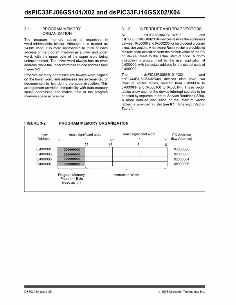
dsPIC33FJ06GS101/X02 and dsPIC33FJ16GSX02/X04
3.1.1 PROGRAM MEMORY ORGANIZATION
The program memory space is organized inword-addressable blocks. Although it is treated as24 bits wide, it is more appropriate to think of eachaddress of the program memory as a lower and upperword, with the upper byte of the upper word beingunimplemented. The lower word always has an evenaddress, while the upper word has an odd address (seeFigure 3-2).
Program memory addresses are always word-alignedon the lower word, and addresses are incremented ordecremented by two during the code execution. Thisarrangement provides compatibility with data memoryspace addressing and makes data in the programmemory space accessible.
3.1.2 INTERRUPT AND TRAP VECTORSAll dsPIC33FJ06GS101/X02 anddsPIC33FJ16GSX02/X04 devices reserve the addressesbetween 0x00000 and 0x000200 for hard-coded programexecution vectors. A hardware Reset vector is provided toredirect code execution from the default value of the PCon device Reset to the actual start of code. A GOTOinstruction is programmed by the user application at0x000000, with the actual address for the start of code at0x000002.
The dsPIC33FJ06GS101/X02 anddsPIC33FJ16GSX02/X04 devices also have twointerrupt vector tables, located from 0x000004 to0x0000FF and 0x000100 to 0x0001FF. These vectortables allow each of the device interrupt sources to behandled by separate Interrupt Service Routines (ISRs).A more detailed discussion of the interrupt vectortables is provided in Section 6.1 “Interrupt VectorTable”.
FIGURE 3-2: PROGRAM MEMORY ORGANIZATION
0816
PC Address
0x0000000x0000020x0000040x000006
230000000000000000
0000000000000000
Program Memory‘Phantom’ Byte
(read as ‘0’)
least significant wordmost significant word
Instruction Width
0x0000010x0000030x0000050x000007
mswAddress (lsw Address)
DS70318A-page 30 © 2008 Microchip Technology Inc.

dsPIC33FJ06GS101/X02 and dsPIC33FJ16GSX02/X04
3.2 Data Address SpaceThe dsPIC33FJ06GS101/X02 anddsPIC33FJ16GSX02/X04 CPU has a separate16-bit-wide data memory space. The data space isaccessed using separate Address Generation Units(AGUs) for read and write operations. The data memorymaps is shown in Figure 3-3.
All Effective Addresses (EAs) in the data memory spaceare 16 bits wide and point to bytes within the data space.This arrangement gives a data space address range of64 Kbytes or 32K words. The lower half of the datamemory space (that is, when EA<15> = 0) is used forimplemented memory addresses, while the upper half(EA<15> = 1) is reserved for the Program SpaceVisibility area (see Section 3.6.3 “Reading Data FromProgram Memory Using Program Space Visibility”).
dsPIC33FJ06GS101/X02 anddsPIC33FJ16GSX02/X04 devices implement up to30 Kbytes of data memory. Should an EA point to alocation outside of this area, an all-zero word or bytewill be returned.
3.2.1 DATA SPACE WIDTHThe data memory space is organized in byteaddressable, 16-bit wide blocks. Data is aligned in datamemory and registers as 16-bit words, but all dataspace EAs resolve to bytes. The Least SignificantBytes (LSBs) of each word have even addresses, whilethe Most Significant Bytes (MSBs) have oddaddresses.
3.2.2 DATA MEMORY ORGANIZATION AND ALIGNMENT
To maintain backward compatibility with PIC® MCUdevices and improve data space memory usageefficiency, the dsPIC33FJ06GS101/X02 anddsPIC33FJ16GSX02/X04 instruction set supports bothword and byte operations. As a consequence of byteaccessibility, all effective address calculations areinternally scaled to step through word-aligned memory.For example, the core recognizes that Post-ModifiedRegister Indirect Addressing mode [Ws++] that resultsin a value of Ws + 1 for byte operations and Ws + 2 forword operations.
Data byte reads will read the complete word thatcontains the byte, using the LSB of any EA todetermine which byte to select. The selected byte isplaced onto the LSB of the data path. That is, datamemory and registers are organized as two parallelbyte-wide entities with shared (word) address decodebut separate write lines. Data byte writes only write tothe corresponding side of the array or register thatmatches the byte address.
All word accesses must be aligned to an even address.Misaligned word data fetches are not supported, socare must be taken when mixing byte and wordoperations, or translating from 8-bit MCU code. If amisaligned read or write is attempted, an address errortrap is generated. If the error occurred on a read, theinstruction underway is completed. If the error occurredon a write, the instruction is executed but the write doesnot occur. In either case, a trap is then executed,allowing the system and/or user application to examinethe machine state prior to execution of the addressFault.
All byte loads into any W register are loaded into theLeast Significant Byte. The Most Significant Byte is notmodified.
A sign-extend instruction (SE) is provided to allow userapplications to translate 8-bit signed data to 16-bitsigned values. Alternatively, for 16-bit unsigned data,user applications can clear the MSB of any W registerby executing a zero-extend (ZE) instruction on theappropriate address.
3.2.3 SFR SPACEThe first 2 Kbytes of the Near Data Space, from 0x0000to 0x07FF, is primarily occupied by Special FunctionRegisters (SFRs). These are used by thedsPIC33FJ06GS101/X02 anddsPIC33FJ16GSX02/X04 core and peripheral modulesfor controlling the operation of the device.
SFRs are distributed among the modules that theycontrol, and are generally grouped together by module.Much of the SFR space contains unused addresses;these are read as ‘0’.
3.2.4 NEAR DATA SPACE The 8 Kbyte area between 0x0000 and 0x1FFF isreferred to as the near data space. Locations in thisspace are directly addressable via a 13-bit absoluteaddress field within all memory direct instructions.Additionally, the whole data space is addressable usingMOV instructions, which support Memory DirectAddressing mode with a 16-bit address field, or byusing Indirect Addressing mode using a workingregister as an address pointer.
Note: The actual set of peripheral features andinterrupts varies by the device. Refer tothe corresponding device tables andpinout diagrams for device-specific information.
© 2008 Microchip Technology Inc. DS70318A-page 31

dsPIC33FJ06GS101/X02 and dsPIC33FJ16GSX02/X04
FIGURE 3-3: DATA MEMORY MAP FOR dsPIC33FJ06GS101/102 DEVICES WITH 256 BYTES OF RAM
0x0000
0x07FE
0x08FE
0xFFFE
LSBAddress16 bits
LSbMSb
MSBAddress
0x0001
0x07FF
0xFFFF
OptionallyMappedinto ProgramMemory
0x0801 0x0800
0x0900
2 KbyteSFR Space
256 bytes
SRAM Space
0x8001 0x8000
SFR Space
X DataUnimplemented (X)
0x087E0x0880
0x087F0x0881
0x08FF0x0901
0x1FFF 0x1FFE0x2001 0x2000
8 KbyteNear DataSpace
X Data RAM (X)
Y Data RAM (Y)
DS70318A-page 32 © 2008 Microchip Technology Inc.

dsPIC33FJ06GS101/X02 and dsPIC33FJ16GSX02/X04
FIGURE 3-4: DATA MEMORY MAP FOR dsPIC33FJ06GS202 DEVICE WITH 1 KB RAM
0x0000
0x07FE
0x0BFE
0xFFFE
LSBAddress16 bits
LSbMSb
MSBAddress
0x0001
0x07FF
0xFFFF
OptionallyMappedinto ProgramMemory
0x0801 0x0800
0x0C00
2 KbyteSFR Space
1Kbyte
SRAM Space
0x8001 0x8000
SFR Space
X DataUnimplemented (X)
0x09FE0x0A00
0x09FF0x0A01
0x0BFF0x0C01
0x1FFF 0x1FFE0x2001 0x2000
8 KbyteNear DataSpace
X Data RAM (X)
Y Data RAM (Y)
© 2008 Microchip Technology Inc. DS70318A-page 33

dsPIC33FJ06GS101/X02 and dsPIC33FJ16GSX02/X04
FIGURE 3-5: DATA MEMORY MAP FOR dsPIC33FJ16GS402/404/502/504 DEVICES WITH 2 KB RAM
0x0000
0x07FE
0x0FFE
0xFFFE
LSBAddress16 bits
LSbMSb
MSBAddress
0x0001
0x07FF
0xFFFF
OptionallyMappedinto ProgramMemory
0x0801 0x0800
0x1000
2 KbyteSFR Space
2 Kbyte
SRAM Space
0x8001 0x8000
SFR Space
X DataUnimplemented (X)
0x0BFE0x0C00
0x0BFF0x0C01
0x0FFF0x1001
0x1FFF 0x1FFE0x2001 0x2000
8 KbyteNear DataSpace
X Data RAM (X)
Y Data RAM (Y)
DS70318A-page 34 © 2008 Microchip Technology Inc.

dsPIC33FJ06GS101/X02 and dsPIC33FJ16GSX02/X04
3.2.5 X AND Y DATA SPACESThe core has two data spaces, X and Y. These dataspaces can be considered either separate (for someDSP instructions), or as one unified linear addressrange (for MCU instructions). The data spaces areaccessed using two Address Generation Units (AGUs)and separate data paths. This feature allows certaininstructions to concurrently fetch two words from RAM,thereby enabling efficient execution of DSP algorithmssuch as Finite Impulse Response (FIR) filtering andFast Fourier Transform (FFT).
The X data space is used by all instructions andsupports all addressing modes. X data space hasseparate read and write data buses. The X read databus is the read data path for all instructions that viewdata space as combined X and Y address space. It isalso the X data prefetch path for the dual operand DSPinstructions (MAC class).
The Y data space is used in concert with the X dataspace by the MAC class of instructions (CLR, ED,EDAC, MAC, MOVSAC, MPY, MPY.N and MSC) toprovide two concurrent data read paths.
Both the X and Y data spaces support ModuloAddressing mode for all instructions, subject toaddressing mode restrictions. Bit-Reversed Addressingmode is only supported for writes to X data space.
All data memory writes, including in DSP instructions,view data space as combined X and Y address space.The boundary between the X and Y data spaces isdevice-dependent and is not user-programmable.
All effective addresses are 16 bits wide and point tobytes within the data space. Therefore, the data spaceaddress range is 64 Kbytes, or 32K words, though theimplemented memory locations vary by device.
© 2008 Microchip Technology Inc. DS70318A-page 35

dsPIC33FJ06G
S101/X02 and dsPIC33FJ16G
SX02/X04
DS
70318A-page 36
© 2008 M
icrochip Technology Inc.
5 Bit 4 Bit 3 Bit 2 Bit 1 Bit 0 All Resets
0000
0000
0000
0000
0000
0000
0000
0000
0000
0000
0000
0000
0000
0000
0000
0800
xxxx
xxxx
xxxxACCAU xxxx
xxxxxxxx
ACCBU xxxx0000
ram Counter High Byte Register 0000
e Page Address Pointer Register 0000
ory Visibility Page Address Pointer Register 0000
xxxx
xxxx
0 xxxx
DOSTARTH<5:0> 00xx
0 xxxx
DOENDH 00xx
0 RA N OV Z C 0000
W ACCSAT IPL3 PSV RND IF 0000
0> XWM<3:0> 0000
TABLE 3-1: CPU CORE REGISTER MAP
SFR Name SFR Addr Bit 15 Bit 14 Bit 13 Bit 12 Bit 11 Bit 10 Bit 9 Bit 8 Bit 7 Bit 6 Bit
WREG0 0000 Working Register 0WREG1 0002 Working Register 1WREG2 0004 Working Register 2WREG3 0006 Working Register 3WREG4 0008 Working Register 4WREG5 000A Working Register 5WREG6 000C Working Register 6WREG7 000E Working Register 7WREG8 0010 Working Register 8WREG9 0012 Working Register 9WREG10 0014 Working Register 10WREG11 0016 Working Register 11WREG12 0018 Working Register 12WREG13 001A Working Register 13WREG14 001C Working Register 14WREG15 001E Working Register 15SPLIM 0020 Stack Pointer Limit Register
ACCAL 0022 ACCAL
ACCAH 0024 ACCAHACCAU 0026 ACCA<39> ACCA<39> ACCA<39> ACCA<39> ACCA<39> ACCA<39> ACCA<39> ACCA<39>ACCBL 0028 ACCBLACCBH 002A ACCBHACCBU 002C ACCB<39> ACCB<39> ACCB<39> ACCB<39> ACCB<39> ACCB<39> ACCB<39> ACCB<39>PCL 002E Program Counter Low Word RegisterPCH 0030 — — — — — — — — Prog
TBLPAG 0032 — — — — — — — — Tabl
PSVPAG 0034 — — — — — — — — Program Mem
RCOUNT 0036 Repeat Loop Counter RegisterDCOUNT 0038 DCOUNT<15:0>DOSTARTL 003A DOSTARTL<15:1>DOSTARTH 003C — — — — — — — — — —DOENDL 003E DOENDL<15:1>DOENDH 0040 — — — — — — — — — —SR 0042 OA OB SA SB OAB SAB DA DC IPL2 IPL1 IPLCORCON 0044 — — — US EDT DL<2:0> SATA SATB SATDMODCON 0046 XMODEN YMODEN — — BWM<3:0> YWM<3:Legend: x = unknown value on Reset, — = unimplemented, read as ‘0’. Reset values are shown in hexadecimal.

© 2008 M
icrochip Technology Inc.D
S70318A
-page 37
dsPIC33FJ06G
S101/X02 and dsPIC33FJ16G
SX02/X04
TA
TA sPIC33FJ16GS402, AND
TA 04
XM 0 xxxx
XM 1 xxxx
YM 0 xxxx
YM 1 xxxx
XB xxxx
DI xxxx
TA
S Bit 4 Bit 3 Bit 2 Bit 1 Bit 0 All Resets
Le
F it 3 Bit 2 Bit 1 Bit 0 All Resets
CN 3IE CN2IE CN1IE CN0IE 0000
CN PUE CN2PUE CN1PUE CN0PUE 0000
Le
N it 3 Bit 2 Bit 1 Bit 0 All Resets
CN N3IE CN2IE CN1IE CN0IE 0000
CN 3PUE CN2PUE CN1PUE CN0PUE 0000
Le
N Bit 3 Bit 2 Bit 1 Bit 0 All Resets
CN CN3IE CN2IE CN1IE CN0IE 0000
CN N19IE CN18IE CN17IE CN16IE 0000
CN N3PUE CN2PUE CN1PUE CN0PUE 0000
CN 19PUE CN18PUE CN17PUE CN16PUE 0000
Le
BLE 3-2: CHANGE NOTIFICATION REGISTER MAP FOR dsPIC33FJ06GS101
BLE 3-3: CHANGE NOTIFICATION REGISTER MAP FOR dsPIC33FJ06GS102, dsPIC33FJ06GS202, ddsPIC33FJ16GS502
BLE 3-4: CHANGE NOTIFICATION REGISTER MAP FOR dsPIC33FJ16GS404 AND dsPIC33FJ16GS5
ODSRT 0048 XS<15:1>ODEND 004A XE<15:1>ODSRT 004C YS<15:1>ODEND 004E YE<15:1>REV 0050 BREN XB<14:0>
SICNT 0052 — — Disable Interrupts Counter Register
BLE 3-1: CPU CORE REGISTER MAP (CONTINUED)
FR Name SFR Addr Bit 15 Bit 14 Bit 13 Bit 12 Bit 11 Bit 10 Bit 9 Bit 8 Bit 7 Bit 6 Bit 5
gend: x = unknown value on Reset, — = unimplemented, read as ‘0’. Reset values are shown in hexadecimal.
ile Name SFR Addr Bit 15 Bit 14 Bit 13 Bit 12 Bit 11 Bit 10 Bit 9 Bit 8 Bit 7 Bit 6 Bit 5 Bit 4 B
EN1 0060 — — — — — — — — CN7IE CN6IE CN5IE CN4IE CN
PU1 0068 — — — — — — — — CN7PUE CN6PUE CN5PUE CN4PUE CN3
gend: x = unknown value on Reset, — = unimplemented, read as ‘0’. Reset values are shown in hexadecimal.
File ame
SFR Addr Bit 15 Bit 14 Bit 13 Bit 12 Bit 11 Bit 10 Bit 9 Bit 8 Bit 7 Bit 6 Bit 5 Bit 4 B
EN1 0060 CN15IE CN14IE CN13IE CN12IE CN11IE CN10IE CN9IE CN8IE CN7IE CN6IE CN5IE CN4IE C
PU1 0068 CN15PUE CN14PUE CN13PUE CN12PUE CN11PUE CN10PUE CN9PUE CN8PUE CN7PUE CN6PUE CN5PUE CN4PUE CN
gend: x = unknown value on Reset, — = unimplemented, read as ‘0’. Reset values are shown in hexadecimal.
File ame
SFR Addr Bit 15 Bit 14 Bit 13 Bit 12 Bit 11 Bit 10 Bit 9 Bit 8 Bit 7 Bit 6 Bit 5 Bit 4
EN1 0060 CN15IE CN14IE CN13IE CN12IE CN11IE CN10IE CN9IE CN8IE CN7IE CN6IE CN5IE CN4IE
EN2 0062 — — CN29IE CN28IE CN27IE CN26IE CN25IE CN24IE CN23IE CN22IE CN21IE CN20IE C
PU1 0068 CN15PUE CN14PUE CN13PUE CN12PUE CN11PUE CN10PUE CN9PUE CN8PUE CN7PUE CN6PUE CN5PUE CN4PUE C
PU2 006A — — CN29PUE CN28PUE CN27PUE CN26PUE CN25PUE CN24PUE CN23PUE CN22PUE CN21PUE CN20PUE CN
gend: x = unknown value on Reset, — = unimplemented, read as ‘0’. Reset values are shown in hexadecimal.
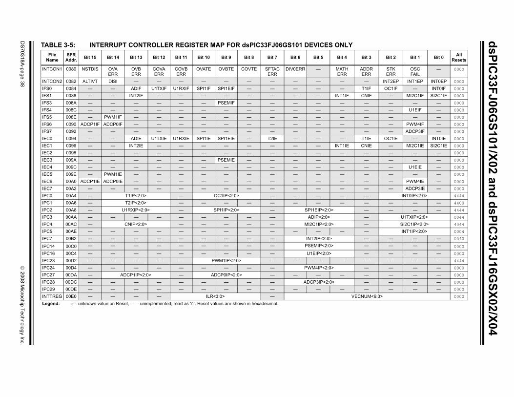
dsPIC33FJ06G
S101/X02 and dsPIC33FJ16G
SX02/X04
DS
70318A-page 38
© 2008 M
icrochip Technology Inc.
Bit 3 Bit 2 Bit 1 Bit 0 All Resets
ADDRERR
STKERR
OSCFAIL
— 0000
— INT2EP INT1EP INT0EP 0000
T1IF OC1IF — INT0IF 0000
CNIF — MI2C1IF SI2C1IF 0000
— — — — 0000
— — U1EIF — 0000
— — — — 0000
— — PWM4IF — 0000
— — ADCP3IF — 0000
T1IE OC1IE — INT0IE 0000
CNIE — MI2C1IE SI2C1IE 0000
— — — — 0000
— — — — 0000
— — U1EIE — 0000
— — — — 0000
— — PWM4IE — 0000
— — ADCP3IE — 0000
— INT0IP<2:0> 4444
— — — — 4400
— — — — 4444
— U1TXIP<2:0> 0044
— SI2C1IP<2:0> 4044
— INT1IP<2:0> 0004
— — — — 0040
— — — — 0000
— — — — 0000
— — — — 4444
— — — — 0000
— — — — 0000
— — — — 0000
— — — — 0000
VECNUM<6:0> 0000
TABLE 3-5: INTERRUPT CONTROLLER REGISTER MAP FOR dsPIC33FJ06GS101 DEVICES ONLYFile
NameSFR Addr. Bit 15 Bit 14 Bit 13 Bit 12 Bit 11 Bit 10 Bit 9 Bit 8 Bit 7 Bit 6 Bit 5 Bit 4
INTCON1 0080 NSTDIS OVAERR
OVBERR
COVAERR
COVBERR
OVATE OVBTE COVTE SFTACERR
DIV0ERR — MATHERR
INTCON2 0082 ALTIVT DISI — — — — — — — — — —IFS0 0084 — — ADIF U1TXIF U1RXIF SPI1IF SPI1EIF — — — — —IFS1 0086 — — INT2IF — — — — — — — — INT1IFIFS3 008A — — — — — — PSEMIF — — — — —IFS4 008C — — — — — — — — — — — —IFS5 008E — PWM1IF — — — — — — — — — —IFS6 0090 ADCP1IF ADCP0IF — — — — — — — — — —IFS7 0092 — — — — — — — — — — — —IEC0 0094 — — ADIE U1TXIE U1RXIE SPI1IE SPI1EIE — T2IE — — —IEC1 0096 — — INT2IE — — — — — — — — INT1IEIEC2 0098 — — — — — — — — — — — —IEC3 009A — — — — — — PSEMIE — — — — —IEC4 009C — — — — — — — — — — — —IEC5 009E — PWM1IE — — — — — — — — — —IEC6 00A0 ADCP1IE ADCP0IE — — — — — — — — — —IEC7 00A2 — — — — — — — — — — — —IPC0 00A4 — T1IP<2:0> — OC1IP<2:0> — — — —IPC1 00A6 — T2IP<2:0> — — — — — — — —IPC2 00A8 — U1RXIP<2:0> — SPI1IP<2:0> — SPI1EIP<2:0>IPC3 00AA — — — — — — — — -— ADIP<2:0>IPC4 00AC — CNIP<2:0> — — — — — MI2C1IP<2:0>IPC5 00AE — — — — — — — — — — — —IPC7 00B2 — — — — — — — — — INT2IP<2:0>
IPC14 00C0 — — — — — — — — — PSEMIP<2:0>
IPC16 00C4 — — — — — — — — — U1EIP<2:0>IPC23 00D2 — — — — — PWM1IP<2:0> — — — —IPC24 00D4 — — — — — — — — — PWM4IP<2:0>IPC27 00DA — ADCP1IP<2:0> — ADCP0IP<2:0> — — — —IPC28 00DC — — — — — — — — — ADCP3IP<2:0>IPC29 00DE — — — — — — — — — — — —INTTREG 00E0 — — — — ILR<3:0> —Legend: x = unknown value on Reset, — = unimplemented, read as ‘0’. Reset values are shown in hexadecimal.

© 2008 M
icrochip Technology Inc.D
S70318A
-page 39
dsPIC33FJ06G
S101/X02 and dsPIC33FJ16G
SX02/X04
TA
N it 3 Bit 2 Bit 1 Bit 0 All Resets
INT DDRRR
STKERR
OSCFAIL
— 0000
IN — INT2EP INT1EP INT0EP 0000
IFS 1IF OC1IF — INT0IF 0000
IFS NIF — MI2C1IF SI2C1IF 0000
IFS — — — — 0000
IFS — — U1EIF — 0000
IFS — — — — 0000
IFS — — — — 0000
IFS — — — ADCP2IF 0000
IEC 1IE OC1IE — INT0IE 0000
IEC NIE — MI2C1IE SI2C1IE 0000
IEC — — — — 0000
IEC — — U1EIE — 0000
IEC — — — — 0000
IEC — — — — 0000
IEC — — — ADCP2IE 0000
IPC — INT0IP<2:0> 4444
IPC — — — — 4400
IPC — — — — 4444
IPC — U1TXIP<2:0> 0044
IPC — SI2C1IP<2:0> 4044
IPC — INT1IP<2:0> 0004
IPC — — — — 0040
IPC — — — — 0000
IPC — — — — 0000
IPC — — — — 4444
IPC — — — — 0000
IPC — — — — 0000
IPC — ADCP2IP<2:0> 0000
IPC — — — — 0000
INT UM<6:0> 0000
Le
BLE 3-6: INTERRUPT CONTROLLER REGISTER MAP FOR dsPIC33FJ06GS102 DEVICES ONLYFile ame
SFR Addr. Bit 15 Bit 14 Bit 13 Bit 12 Bit 11 Bit 10 Bit 9 Bit 8 Bit 7 Bit 6 Bit 5 Bit 4 B
CON1 0080 NSTDIS OVAERR
OVBERR
COVAERR
COVBERR
OVATE OVBTE COVTE SFTACERR
DIV0ERR
— MATHERR
AE
TCON2 0082 ALTIVT DISI — — — — — — — — — —0 0084 — — ADIF U1TXIF U1RXIF SPI1IF SPI1EIF — T2IF — — — T1 0086 — — INT2IF — — — — — — — — INT1IF C3 008A — — — — — — PSEMIF — — — — —4 008C — — — — — — — — — — — —5 008E PWM2IF PWM1IF — — — — — — — — — —6 0090 ADCP1IF ADCP0IF — — — — — — — — — —7 0092 — — — — — — — — — — — —0 0094 — — ADIE U1TXIE U1RXIE SPI1IE SPI1EIE — T2IE — — — T1 0096 — — INT2IE — — — — — — — — INT1IE C3 009A — — — — — — PSEMIE — — — — —4 009C — — — — — — — — — — — —5 009E PWM2IE PWM1IE — — — — — — — — — —6 00A0 ADCP1IE ADCP0IE — — — — — — — — — —7 00A2 — — — — — — — — — — — —0 00A4 — T1IP<2:0> — OC1IP<2:0> — — — —1 00A6 — T2IP<2:0> — — — — — — — —2 00A8 — U1RXIP<2:0> — SPI1IP<2:0> — SPI1EIP<2:0>3 00AA — — — — — — — — -— ADIP<2:0>4 00AC — CNIP<2:0> — — — — — MI2C1IP<2:0>5 00AE — — — — — — — — — — — —7 00B2 — — — — — — — — — INT2IP<2:0>
14 00C0 — — — — — — — — — PSEMIP<2:0>
16 00C4 — — — — — — — — — U1EIP<2:0>23 00D2 — PWM2IP<2:0> — PWM1IP<2:0> — — — —24 00D4 — — — — — — — — — — — —27 00DA — ADCP1IP<2:0> — ADCP0IP<2:0> — — — —28 00DC — — — — — — — — — — — —29 00DE — — — — — — — — — — — —TREG 00E0 — — — — ILR<3:0> — VECN
gend: x = unknown value on Reset, — = unimplemented, read as ‘0’. Reset values are shown in hexadecimal.

dsPIC33FJ06G
S101/X02 and dsPIC33FJ16G
SX02/X04
DS
70318A-page 40
© 2008 M
icrochip Technology Inc.
Bit 3 Bit 2 Bit 1 Bit 0 All Resets
ADDRERR
STKERR
OSCFAIL
— 0000
— INT2EP INT1EP INT0EP 0000
T1IF OC1IF IC1IF INT0IF 0000
CNIF AC1IF MI2C1IF SI2C1IF 0000
— — — — 0000
— — U1EIF — 0000
— — — — 0000
— — — — 0000
— — — ADCP2IF 0000
T1IE OC1IE IC1IE INT0IE 0000
CNIE AC1IE MI2C1IE SI2C1IE 0000
— — — — 0000
— — U1EIE — 0000
— — — — 0000
— — — — 0000
— — — ADCP2IE 0000
— INT0IP<2:0> 4444
— — — — 4400
— — — — 4444
— U1TXIP<2:0> 0044
— SI2C1IP<2:0> 4044
— INT1IP<2:0> 0004
— — — — 0040
— — — — 0000
— — — — 0000
— — — — 4444
— — — — 0000
— — — — 4444
— — — — 0000
— ADCP2IP<2:0> 0000
VECNUM<6:0> 0000
TABLE 3-7: INTERRUPT CONTROLLER REGISTER MAP FOR dsPIC33FJ06G202 DEVICES ONLYFile
NameSFR Addr. Bit 15 Bit 14 Bit 13 Bit 12 Bit 11 Bit 10 Bit 9 Bit 8 Bit 7 Bit 6 Bit 5 Bit 4
INTCON1 0080 NSTDIS OVAERR
OVBERR
COVAERR
COVBERR
OVATE OVBTE COVTE SFTACERR
DIV0ERR
— MATHERR
INTCON2 0082 ALTIVT DISI — — — — — — — — — —IFS0 0084 — — ADIF U1TXIF U1RXIF SPI1IF SPI1EIF — T2IF — — —IFS1 0086 — — INT2IF — — — — — — — — INT1IFIFS3 008A — — — — — — PSEMIF — — — — —IFS4 008C — — — — — — — — — — — —IFS5 008E PWM2IF PWM1IF — — — — — — — — — —IFS6 0090 ADCP1IF ADCP0IF — — — — — — AC2IF — — —IFS7 0092 — — — — — — — — — — — ADCP6IFIEC0 0094 — — ADIE U1TXIE U1RXIE SPI1IE SPI1EIE — T2IE — — —IEC1 0096 — — INT2IE — — — — — — — — INT1IEIEC3 009A — — — — — — PSEMIE — — — — —IEC4 009C — — — — — — — — — — — —IEC5 009E PWM2IE PWM1IE — — — — — — — — — —IEC6 00A0 ADCP1IE ADCP0IE — — — — — — AC2IE — — —IEC7 00A2 — — — — — — — — — — — ADCP6IEIPC0 00A4 — T1IP<2:0> — OC1IP<2:0> — IC1IP<2:0>IPC1 00A6 — T2IP<2:0> — — — — — — — —IPC2 00A8 — U1RXIP<2:0> — SPI1IP<2:0> — SPI1EIP<2:0>IPC3 00AA — — — — — — — — -— ADIP<2:0>IPC4 00AC — CNIP<2:0> — AC1IP<2:0> — MI2C1IP<2:0>IPC5 00AE — — — — — — — — — — — —IPC7 00B2 — — — — — — — — — INT2IP<2:0>
IPC14 00C0 — — — — — — — — — PSEMIP<2:0>
IPC16 00C4 — — — — — — — — — U1EIP<2:0>IPC23 00D2 — PWM2IP<2:0> — PWM1IP<2:0> — — — —IPC24 00D4 — — — — — — — — — — — —IPC25 00D6 — AC2IP<2:0> — — — — — — — —IPC27 00DA — ADCP1IP<2:0> — ADCP0IP<2:0> — — — —IPC28 00DC — — — — — — — — — — — —INTTREG 00E0 — — — — ILR<3:0> —Legend: x = unknown value on Reset, — = unimplemented, read as ‘0’. Reset values are shown in hexadecimal.

© 2008 M
icrochip Technology Inc.D
S70318A
-page 41
dsPIC33FJ06G
S101/X02 and dsPIC33FJ16G
SX02/X04
TA
N it 3 Bit 2 Bit 1 Bit 0 All Resets
INT DDRRR
STKERR
OSCFAIL
— 0000
IN — INT2EP INT1EP INT0EP 0000
IFS 1IF OC1IF IC1IF INT0IF 0000
IFS NIF — MI2C1IF SI2C1IF 0000
IFS — — — — 0000
IFS — — U1EIF — 0000
IFS — — — — 0000
IFS — — — PWM3IF 0000
IFS — — ADCP3IF ADCP2IF 0000
IEC 1IE OC1IE IC1IE INT0IE 0000
IEC NIE — MI2C1IE SI2C1IE 0000
IEC — — — — 0000
IEC — — U1EIE — 0000
IEC — — — — 0000
IEC — — — PWM3IE 0000
IEC — — ADCP3IE ADCP2IE 0000
IPC — INT0IP<2:0> 4444
IPC — — — — 4400
IPC — T3IP<2:0> 4444
IPC — U1TXIP<2:0> 0044
IPC — SI2C1IP<2:0> 4044
IPC — INT1IP<2:0> 0004
IPC — — — — 0040
IPC — — — — 0000
IPC — — — — 0000
IPC — — — — 4444
IPC — PWM3IP<2:0> 0000
IPC — — — — 0000
IPC — ADCP2IP<2:0> 0000
INT UM<6:0> 0000
Le
BLE 3-8: INTERRUPT CONTROLLER REGISTER MAP FOR dsPIC33FJ16GS402/404 DEVICES ONLYFile ame
SFR Addr. Bit 15 Bit 14 Bit 13 Bit 12 Bit 11 Bit 10 Bit 9 Bit 8 Bit 7 Bit 6 Bit 5 Bit 4 B
CON1 0080 NSTDIS OVAERR
OVBERR
COVAERR
COVBERR
OVATE OVBTE COVTE SFTACERR
DIV0ERR
— MATHERR
AE
TCON2 0082 ALTIVT DISI — — — — — — — — — —0 0084 — — ADIF U1TXIF U1RXIF SPI1IF SPI1EIF T3IF T2IF OC2IF IC2IF — T1 0086 — — INT2IF — — — — — — — — INT1IF C3 008A — — — — — — PSEMIF — — — — —4 008C — — — — — — — — — — — —5 008E PWM2IF PWM1IF — — — — — — — — — —6 0090 ADCP1IF ADCP0IF — — — — — — — — — —7 0092 — — — — — — — — — — — —0 0094 — — ADIE U1TXIE U1RXIE SPI1IE SPI1EIE T3IE T2IE OC2IE IC2IE — T1 0096 — — INT2IE — — — — — — — — INT1IE C3 009A — — — — — — PSEMIE — — — — —4 009C — — — — — — — — — — — —5 009E PWM2IE PWM1IE — — — — — — — — — —6 00A0 ADCP1IE ADCP0IE — — — — — — — — — —7 00A2 — — — — — — — — — — — —0 00A4 — T1IP<2:0> — OC1IP<2:0> — IC1IP<2:0>1 00A6 — T2IP<2:0> — OC2IP<2:0> — IC2IP<2:0>2 00A8 — U1RXIP<2:0> — SPI1IP<2:0> — SPI1EIP<2:0>3 00AA — — — — — — — — -— ADIP<2:0>4 00AC — CNIP<2:0> — — — — — MI2C1IP<2:0>5 00AE — — — — — — — — — — — —7 00B2 — — — — — — — — — INT2IP<2:0>
14 00C0 — — — — — — — — — PSEMIP<2:0>
16 00C4 — — — — — — — — — U1EIP<2:0>23 00D2 — PWM2IP<2:0> — PWM1IP<2:0> -— —24 00D4 — — — — — — — — — — — —27 00DA — ADCP1IP<2:0> — ADCP0IP<2:0> -— —28 00DC — — — — — — — — — ADCP3IP<2:0>TREG 00E0 — — — — ILR<3:0> — VECN
gend: x = unknown value on Reset, — = unimplemented, read as ‘0’. Reset values are shown in hexadecimal.

dsPIC33FJ06G
S101/X02 and dsPIC33FJ16G
SX02/X04
DS
70318A-page 42
© 2008 M
icrochip Technology Inc.
Bit 3 Bit 2 Bit 1 Bit 0 All Resets
ADDRERR
STKERR
OSCFAIL
— 0000
— INT2EP INT1EP INT0EP 0000
T1IF OC1IF IC1IF INT0IF 0000
CNIF AC1IF MI2C1IF SI2C1IF 0000
— — — — 0000
— — U1EIF — 0000
— — — — 0000
— — PWM4IF PWM3IF 0000
— — ADCP3IF ADCP2IF 0000
T1IE OC1IE IC1IE INT0IE 0000
CNIE AC1IE MI2C1IE SI2C1IE 0000
— — — — 0000
— — U1EIE — 0000
— — — — 0000
— — PWM4IE PWM3IE 0000
— — ADCP3IE ADCP2IE 0000
— INT0IP<2:0> 4444
-— — — — 4400
— T3IP<2:0> 4444
— U1TXIP<2:0> 0044
— SI2C1IP<2:0> 4044
— INT1IP<2:0> 0004
— — — — 0040
— — — — 0000
— — — — 0000
— — — — 4444
— PWM3IP<2:0> 0000
— — — — 4444
— AC3IP<2:0> 0444
— — — — 0000
— ADCP2IP<2:0> 0000
— ADCP6IP<2:0> 0000
VECNUM<6:0> 0000
TABLE 3-9: INTERRUPT CONTROLLER REGISTER MAP FOR dsPIC33FJ16GS502 DEVICES ONLYFile
NameSFR Addr. Bit 15 Bit 14 Bit 13 Bit 12 Bit 11 Bit 10 Bit 9 Bit 8 Bit 7 Bit 6 Bit 5 Bit 4
INTCON1 0080 NSTDIS OVAERR
OVBERR
COVAERR
COVBERR
OVATE OVBTE COVTE SFTACERR
DIV0ERR
— MATHERR
INTCON2 0082 ALTIVT DISI — — — — — — — — — —IFS0 0084 — — ADIF U1TXIF U1RXIF SPI1IF SPI1EIF T3IF T2IF OC2IF IC2IF —IFS1 0086 — — INT2IF — — — — — — — — INT1IFIFS3 008A — — — — — — PSEMIF — — — — —IFS4 008C — — — — — — — — — — — —IFS5 008E PWM2IF PWM1IF — — — — — — — — — —IFS6 0090 ADCP1IF ADCP0IF — — — — AC4IF AC3IF AC2IF — — —IFS7 0092 — — — — — — — — — — — ADCP6IFIEC0 0094 — — ADIE U1TXIE U1RXIE SPI1IE SPI1EIE T3IE T2IE OC2IE IC2IE —IEC1 0096 — — INT2IE — — — — — — — — INT1IEIEC3 009A — — — — — — PSEMIE — — — — —IEC4 009C — — — — — — — — — — — —IEC5 009E PWM2IE PWM1IE — — — — — — — — — —IEC6 00A0 ADCP1IE ADCP0IE — — — — AC4IE AC3IE AC2IE — — —IEC7 00A2 — — — — — — — — — — — ADCP6IEIPC0 00A4 — T1IP<2:0> — OC1IP<2:0> — IC1IP<2:0>IPC1 00A6 — T2IP<2:0> — OC2IP<2:0> — IC2IP<2:0>IPC2 00A8 — U1RXIP<2:0> — SPI1IP<2:0> — SPI1EIP<2:0>IPC3 00AA — — — — -— — -— ADIP<2:0>IPC4 00AC — CNIP<2:0> — AC1IP<2:0> — MI2C1IP<2:0>IPC5 00AE — — — — — — — — — — — —IPC7 00B2 — — — — — — — — — INT2IP<2:0>
IPC14 00C0 — — — — — — — — — PSEMIP<2:0>
IPC16 00C4 — — — — — — — — — U1EIP<2:0>IPC23 00D2 — PWM2IP<2:0> — PWM1IP<2:0> — — — —IPC24 00D4 — — — — — — — — — PWM4IP<2:0>IPC25 00D6 — AC2IP<2:0> — — — — — — — —IPC26 00D8 — — — — — — — — — AC4IP<2:0>IPC27 00DA — ADCP1IP<2:0> — ADCP0IP<2:0> -— —IPC28 00DC — — — — — — — — — ADCP3IP<2:0>IPC29 00DE — — — — — — — — — — — —INTTREG 00E0 — — — — ILR<3:0> —Legend: x = unknown value on Reset, — = unimplemented, read as ‘0’. Reset values are shown in hexadecimal.

© 2008 M
icrochip Technology Inc.D
S70318A
-page 43
dsPIC33FJ06G
S101/X02 and dsPIC33FJ16G
SX02/X04
TA
N it 3 Bit 2 Bit 1 Bit 0 All Resets
INT DDRRR
STKERR
OSCFAIL
— 0000
IN — INT2EP INT1EP INT0EP 0000
IFS 1IF OC1IF IC1IF INT0IF 0000
IFS NIF AC1IF MI2C1IF SI2C1IF 0000
IFS — — — — 0000
IFS — — U1EIF — 0000
IFS — — — — 0000
IFS — — PWM4IF PWM3IF 0000
IFS CP5IF ADCP4IF ADCP3IF ADCP2IF 0000
IEC 1IE OC1IE IC1IE INT0IE 0000
IEC NIE AC1IE MI2C1IE SI2C1IE 0000
IEC — — — — 0000
IEC — — U1EIE — 0000
IEC — — — — 0000
IEC — — PWM4IE PWM3IE 0000
IEC CP5IE ADCP4IE ADCP3IE ADCP2IE 0000
IPC — INT0IP<2:0> 4444
IPC — — — — 4400
IPC — T3IP<2:0> 4444
IPC — U1TXIP<2:0> 0044
IPC — SI2C1IP<2:0> 4044
IPC — INT1IP<2:0> 0004
IPC — — — — 0040
IPC — — — — 0000
IPC — — — — 0000
IPC — — — — 4444
IPC — PWM3IP<2:0> 0000
IPC — — — — 4444
IPC — AC3IP<2:0> 0444
IPC — — — — 0000
IPC — ADCP2IP<2:0> 0000
IPC — ADCP6IP<2:0> 0000
INT UM<6:0> 0000
Le
BLE 3-10: INTERRUPT CONTROLLER REGISTER MAP FOR dsPIC33FJ16GS504 DEVICES ONLYFile ame
SFR Addr. Bit 15 Bit 14 Bit 13 Bit 12 Bit 11 Bit 10 Bit 9 Bit 8 Bit 7 Bit 6 Bit 5 Bit 4 B
CON1 0080 NSTDIS OVAERR
OVBERR
COVAERR
COVBERR
OVATE OVBTE COVTE SFTACERR
DIV0ERR
— MATHERR
AE
TCON2 0082 ALTIVT DISI — — — — — — — — — —0 0084 — — ADIF U1TXIF U1RXIF SPI1IF SPI1EIF T3IF T2IF OC2IF IC2IF — T1 0086 — — INT2IF — — — — — — — — INT1IF C3 008A — — — — — — PSEMIF — — — — —4 008C — — — — — — — — — — — —5 008E PWM2IF PWM1IF — — — — — — — — — —6 0090 ADCP1IF ADCP0IF — — — — AC4IF AC3IF AC2IF — — —7 0092 — — — — — — — — — — — ADCP6IF AD0 0094 — — ADIE U1TXIE U1RXIE SPI1IE SPI1EIE T3IE T2IE OC2IE IC2IE — T1 0096 — — INT2IE — — — — — — — — INT1IE C3 009A — — — — — — PSEMIE — — — — —4 009C — — — — — — — — — — — —5 009E PWM2IE PWM1IE — — — — — — — — — —6 00A0 ADCP1IE ADCP0IE — — — — AC4IE AC3IE AC2IE — — —7 00A2 — — — — — — — — — — — ADCP6IE AD0 00A4 — T1IP<2:0> — OC1IP<2:0> — IC1IP<2:0>1 00A6 — T2IP<2:0> — OC2IP<2:0> — IC2IP<2:0>2 00A8 — U1RXIP<2:0> — SPI1IP<2:0> — SPI1EIP<2:0>3 00AA — — — — — — — — -— ADIP<2:0>4 00AC — CNIP<2:0> — AC1IP<2:0> — MI2C1IP<2:0>5 00AE — — — — — — — — — — — —7 00B2 — — — — — — — — — INT2IP<2:0>
14 00C0 — — — — — — — — — PSEMIP<2:0>
16 00C4 — — — — — — — — — U1EIP<2:0>23 00D2 — PWM2IP<2:0> — PWM1IP<2:0> — — — —24 00D4 — — — — — — — — — PWM4IP<2:0>25 00D6 — AC2IP<2:0> — — — — — — — —26 00D8 — — — — — — — — — AC4IP<2:0>27 00DA — ADCP1IP<2:0> — ADCP0IP<2:0> — — — —28 00DC — ADCP5IP<2:0> — ADCP4IP<2:0> — ADCP3IP<2:0>29 00DE — — — — — — — — — — — —TREG 00E0 — — — — ILR<3:0> — VECN
gend: x = unknown value on Reset, — = unimplemented, read as ‘0’. Reset values are shown in hexadecimal.
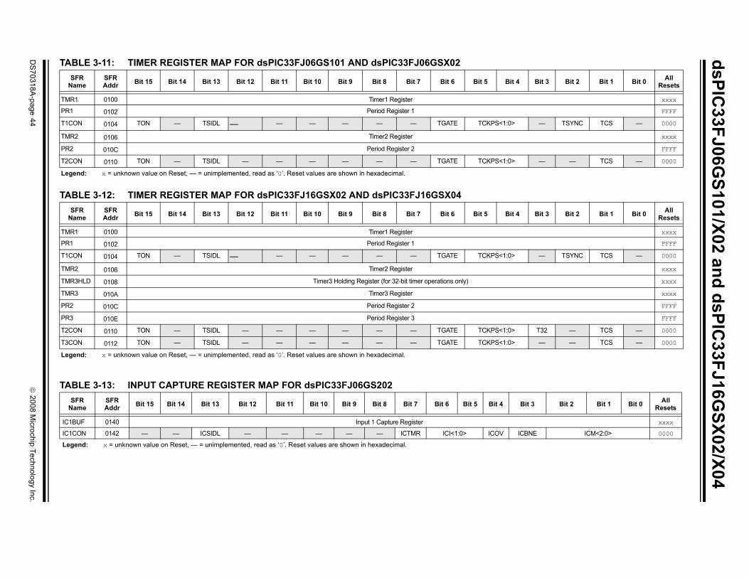
dsPIC33FJ06G
S101/X02 and dsPIC33FJ16G
SX02/X04
DS
70318A-page 44
© 2008 M
icrochip Technology Inc.
t 4 Bit 3 Bit 2 Bit 1 Bit 0 All Resets
xxxx
FFFF
> — TSYNC TCS — 0000
xxxx
FFFF
> — — TCS — 0000
t 4 Bit 3 Bit 2 Bit 1 Bit 0 All Resets
xxxx
FFFF
> — TSYNC TCS — 0000
xxxx
xxxx
xxxx
FFFF
FFFF
> T32 — TCS — 0000
> — — TCS — 0000
Bit 3 Bit 2 Bit 1 Bit 0 All Resets
xxxx
ICBNE ICM<2:0> 0000
TABLE 3-11: TIMER REGISTER MAP FOR dsPIC33FJ06GS101 AND dsPIC33FJ06GSX02
TABLE 3-12: TIMER REGISTER MAP FOR dsPIC33FJ16GSX02 AND dsPIC33FJ16GSX04
SFR Name
SFR Addr Bit 15 Bit 14 Bit 13 Bit 12 Bit 11 Bit 10 Bit 9 Bit 8 Bit 7 Bit 6 Bit 5 Bi
TMR1 0100 Timer1 Register
PR1 0102 Period Register 1
T1CON 0104 TON — TSIDL — — — — — — TGATE TCKPS<1:0
TMR2 0106 Timer2 Register
PR2 010C Period Register 2
T2CON 0110 TON — TSIDL — — — — — — TGATE TCKPS<1:0
Legend: x = unknown value on Reset, — = unimplemented, read as ‘0’. Reset values are shown in hexadecimal.
SFR Name
SFR Addr Bit 15 Bit 14 Bit 13 Bit 12 Bit 11 Bit 10 Bit 9 Bit 8 Bit 7 Bit 6 Bit 5 Bi
TMR1 0100 Timer1 Register
PR1 0102 Period Register 1
T1CON 0104 TON — TSIDL — — — — — — TGATE TCKPS<1:0
TMR2 0106 Timer2 Register
TMR3HLD 0108 Timer3 Holding Register (for 32-bit timer operations only)
TMR3 010A Timer3 Register
PR2 010C Period Register 2
PR3 010E Period Register 3
T2CON 0110 TON — TSIDL — — — — — — TGATE TCKPS<1:0
T3CON 0112 TON — TSIDL — — — — — — TGATE TCKPS<1:0
Legend: x = unknown value on Reset, — = unimplemented, read as ‘0’. Reset values are shown in hexadecimal.
TABLE 3-13: INPUT CAPTURE REGISTER MAP FOR dsPIC33FJ06GS202SFR
NameSFR Addr Bit 15 Bit 14 Bit 13 Bit 12 Bit 11 Bit 10 Bit 9 Bit 8 Bit 7 Bit 6 Bit 5 Bit 4
IC1BUF 0140 Input 1 Capture Register
IC1CON 0142 — — ICSIDL — — — — — ICTMR ICI<1:0> ICOV
Legend: x = unknown value on Reset, — = unimplemented, read as ‘0’. Reset values are shown in hexadecimal.

© 2008 M
icrochip Technology Inc.D
S70318A
-page 45
dsPIC33FJ06G
S101/X02 and dsPIC33FJ16G
SX02/X04
TA
TA
N t 3 Bit 2 Bit 1 Bit 0 All Resets
IC xxxx
IC NE ICM<2:0> 0000
IC xxxx
IC NE ICM<2:0> 0000
Le
TA
N Bit 3 Bit 2 Bit 1 Bit 0 All Resets
OC xxxx
OC xxxx
OC OCTSEL OCM<2:0> 0000
Le
N Bit 3 Bit 2 Bit 1 Bit 0 All Resets
OC xxxxOC xxxxOC OCTSEL OCM<2:0> 0000
OC xxxxOC xxxxxOC OCTSEL OCM<2:0> 0000
Le
BLE 3-14: INPUT CAPTURE REGISTER MAP FOR dsPIC33FJ16GSX02 AND dsPIC33FJ16GSX04
BLE 3-16: OUTPUT COMPARE REGISTER MAP dsPIC33FJ06GSX02 AND dsPIC33FJ06GSX04
SFR ame SFR Addr Bit 15 Bit 14 Bit 13 Bit 12 Bit 11 Bit 10 Bit 9 Bit 8 Bit 7 Bit 6 Bit 5 Bit 4 Bi
1BUF 0140 Input 1 Capture Register
1CON 0142 — — ICSIDL — — — — — ICTMR ICI<1:0> ICOV ICB
2BUF 0144 Input 2 Capture Register
2CON 0146 — — ICSIDL — — — — — ICTMR ICI<1:0> ICOV ICB
gend: x = unknown value on Reset, — = unimplemented, read as ‘0’. Reset values are shown in hexadecimal.
BLE 3-15: OUTPUT COMPARE REGISTER MAP dsPIC33FJ06GS101 AND dsPIC33FJ06GSX02SFR ame
SFR Addr Bit 15 Bit 14 Bit 13 Bit 12 Bit 11 Bit 10 Bit 9 Bit 8 Bit 7 Bit 6 Bit 5 Bit 4
1RS 0180 Output Compare 1 Secondary Register
1R 0182 Output Compare 1 Register
1CON 0184 — — OCSIDL — — — — — — — — OCFLT
gend: x = unknown value on Reset, — = unimplemented, read as ‘0’. Reset values are shown in hexadecimal.
SFR ame
SFR Addr Bit 15 Bit 14 Bit 13 Bit 12 Bit 11 Bit 10 Bit 9 Bit 8 Bit 7 Bit 6 Bit 5 Bit 4
1RS 0180 Output Compare 1 Secondary Register
1R 0182 Output Compare 1 Register
1CON 0184 — — OCSIDL — — — — — — — — OCFLT
2RS 0186 Output Compare 2 Secondary Register
2R 0188 Output Compare 2 Register
2CON 018A — — OCSIDL — — — — — — — — OCFLT
gend: x = unknown value on Reset, — = unimplemented, read as ‘0’. Reset values are shown in hexadecimal.

dsPIC33FJ06G
S101/X02 and dsPIC33FJ16G
SX02/X04
DS
70318A-page 46
© 2008 M
icrochip Technology Inc.
Bit 4 Bit 3 Bit 2 Bit 1 Bit 0 All Resets
<1:0> SEVTPS<3:0> 0000
— — PCLKDIV<2:0> 0000
FFF8
— — — 0000
0000
Bit 4 Bit 3 Bit 2 Bit 1 Bit 0 All Resets
— — CAM XPRES IUE 0000
1:0> CLDAT<1:0> SWAP OSYNC 0000
FLTPOL FLTMOD<1:0> 0000
0000
0000
0000
0000
0000
0000
— — — 0000
TRGSTRT<5:0> 0000
— — — 0000
— — — 0000
— — — 0000
TABLE 3-17: HIGH-SPEED PWM REGISTER MAP
File Name Addr Offset Bit 15 Bit 14 Bit 13 Bit 12 Bit 11 Bit 10 Bit 9 Bit 8 Bit 7 Bit 6 Bit 5
PTCON 0400 PTEN — PTSIDL SESTAT SEIEN EIPU SYNCPOL SYNCOEN SYNCEN — SYNCSRC
PTCON2 0402 — — — — — — — — — — —
PTPER 0404 PTPER<15:0>
SEVTCMP 0406 SEVTCMP<15:3>
MDC 040A MDC<15:0>
Legend: x = unknown value on Reset, — = unimplemented, read as ‘0’. Reset values are shown in hexadecimal.
TABLE 3-18: HIGH-SPEED PWM GENERATOR 1 REGISTER MAP
File Name Addr Offset Bit 15 Bit 14 Bit 13 Bit 12 Bit 11 Bit 10 Bit 9 Bit 8 Bit 7 Bit 6 Bit 5
PWMCON1 0420 FLTSTAT CLSTAT TRGSTAT FLTIEN CLIEN TRGIEN ITB MDCS DTC<1:0> —
IOCON1 0422 PENH PENL POLH POLL PMOD<1:0> OVRENH OVRENL OVRDAT<1:0> FLTDAT<
FCLCON1 0424 IFLTMOD CLSRC<4:0> CLPOL CLMOD FLTSRC<4:0>
PDC1 0426 PDC1<15:0>
PHASE1 0428 PHASE1<15:0>
DTR1 042A — — DTR1<13:0>
ALTDTR1 042C — — ALTDTR1<13:0>
SDC1 042E SDC1<15:0>
SPHASE1 0430 SPHASE1<15:0>
TRIG1 0432 TRGCMP<15:3>
TRGCON1 0434 TRGDIV<3:0> — — — — DTM —
STRIG1 0436 STRGCMP<15:3>
PWMCAP1 0438 PWMCAP1<15:3>
LEBCON1 043A PHR PHF PLR PLF FLTLEBEN CLLEBEN LEB<9:3>
Legend: x = unknown value on Reset, — = unimplemented, read as ‘0’. Reset values are shown in hexadecimal.

© 2008 M
icrochip Technology Inc.D
S70318A
-page 47
dsPIC33FJ06G
S101/X02 and dsPIC33FJ16G
SX02/X04
TA IC33FJ16X02/X04 DEVICES ONLY
Fi Bit 3 Bit 2 Bit 1 Bit 0 All Resets
PW — CAM XPRES IUE 0000
IO CLDAT<1:0> SWAP OSYNC 0000
FC FLTPOL FLTMOD<1:0> 0000
PD 0000
PH 0000
DT 0000
AL 0000
SD 0000
SP 0000
TR — — — 0000
TR TRGSTRT<5:0> 0000
ST — — — 0000
PW — — — 0000
LE — — — 0000
Le
BLE 3-19: HIGH-SPEED PWM GENERATOR 2 REGISTER MAP FOR dsPIC33FJ06GS102/202 AND dsP
le Name Addr Offset Bit 15 Bit 14 Bit 13 Bit 12 Bit 11 Bit 10 Bit 9 Bit 8 Bit 7 Bit 6 Bit 5 Bit 4
MCON2 0440 FLTSTAT CLSTAT TRGSTAT FLTIEN CLIEN TRGIEN ITB MDCS DTC<1:0> — —
CON2 0442 PENH PENL POLH POLL PMOD<1:0> OVRENH OVRENL OVRDAT<1:0> FLTDAT<1:0>
LCON2 0444 IFLTMOD CLSRC<4:0> CLPOL CLMOD FLTSRC<4:0>
C2 0446 PDC2<15:0>
ASE2 0448 PHASE2<15:0>
R2 044A — — DTR2<13:0>
TDTR2 044C — — ALTDTR2<13:0>
C2 044E SDC2<15:0>
HASE2 0450 SPHASE2<15:0>
IG2 0452 TRGCMP<15:3>
GCON2 0454 TRGDIV<3:0> — — — — DTM —
RIG2 0456 STRGCMP<15:3>
MCAP2 0458 PWMCAP2<15:3>
BCON2 045A PHR PHF PLR PLF FLTLEBEN CLLEBEN LEB<9:3>
gend: x = unknown value on Reset, — = unimplemented, read as ‘0’. Reset values are shown in hexadecimal.
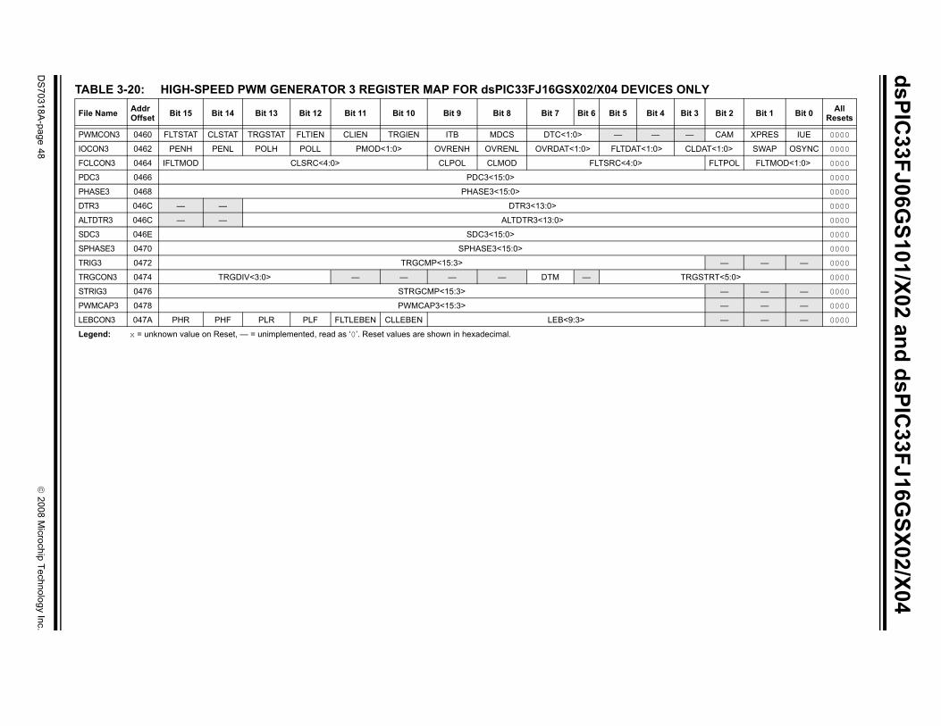
dsPIC33FJ06G
S101/X02 and dsPIC33FJ16G
SX02/X04
DS
70318A-page 48
© 2008 M
icrochip Technology Inc.
ICES ONLY
Bit 4 Bit 3 Bit 2 Bit 1 Bit 0 All Resets
— — CAM XPRES IUE 0000
1:0> CLDAT<1:0> SWAP OSYNC 0000
FLTPOL FLTMOD<1:0> 0000
0000
0000
0000
0000
0000
0000
— — — 0000
TRGSTRT<5:0> 0000
— — — 0000
— — — 0000
— — — 0000
TABLE 3-20: HIGH-SPEED PWM GENERATOR 3 REGISTER MAP FOR dsPIC33FJ16GSX02/X04 DEV
File Name Addr Offset Bit 15 Bit 14 Bit 13 Bit 12 Bit 11 Bit 10 Bit 9 Bit 8 Bit 7 Bit 6 Bit 5
PWMCON3 0460 FLTSTAT CLSTAT TRGSTAT FLTIEN CLIEN TRGIEN ITB MDCS DTC<1:0> —
IOCON3 0462 PENH PENL POLH POLL PMOD<1:0> OVRENH OVRENL OVRDAT<1:0> FLTDAT<
FCLCON3 0464 IFLTMOD CLSRC<4:0> CLPOL CLMOD FLTSRC<4:0>
PDC3 0466 PDC3<15:0>
PHASE3 0468 PHASE3<15:0>
DTR3 046C — — DTR3<13:0>
ALTDTR3 046C — — ALTDTR3<13:0>
SDC3 046E SDC3<15:0>
SPHASE3 0470 SPHASE3<15:0>
TRIG3 0472 TRGCMP<15:3>
TRGCON3 0474 TRGDIV<3:0> — — — — DTM —
STRIG3 0476 STRGCMP<15:3>
PWMCAP3 0478 PWMCAP3<15:3>
LEBCON3 047A PHR PHF PLR PLF FLTLEBEN CLLEBEN LEB<9:3>
Legend: x = unknown value on Reset, — = unimplemented, read as ‘0’. Reset values are shown in hexadecimal.
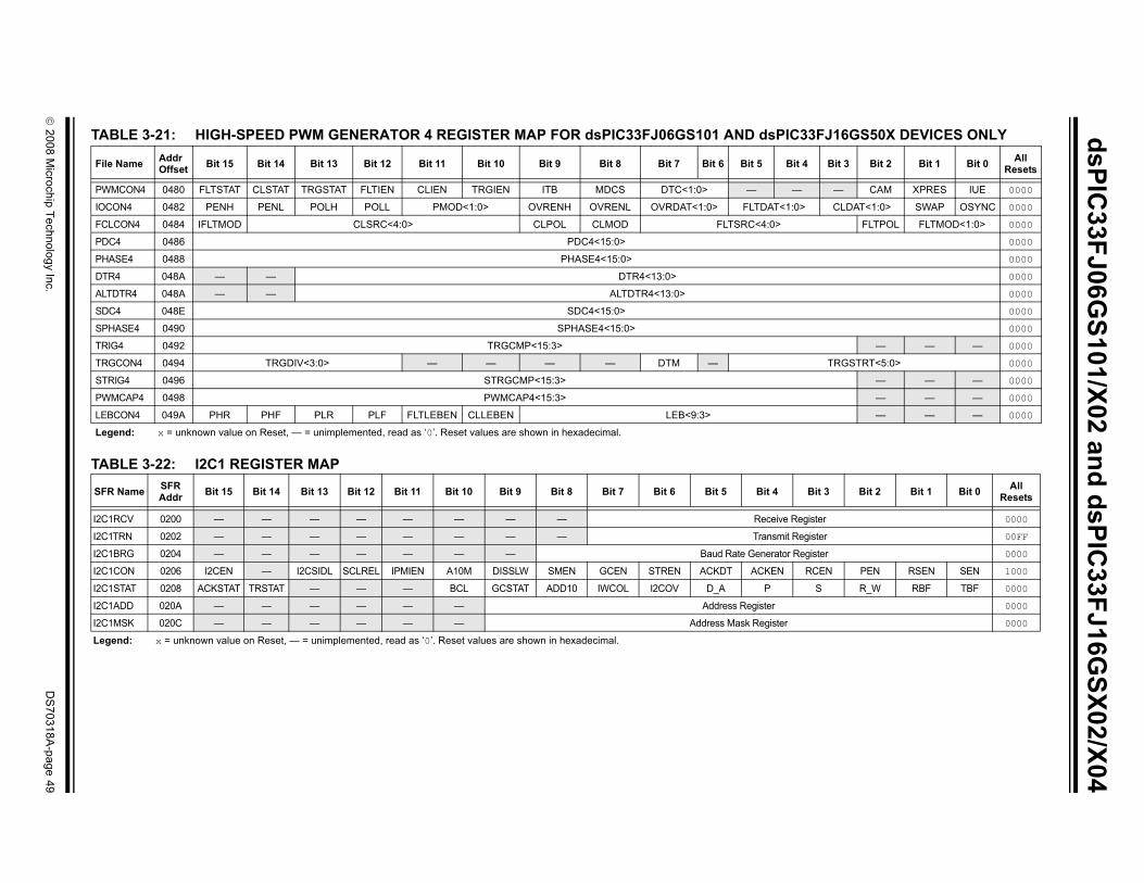
© 2008 M
icrochip Technology Inc.D
S70318A
-page 49
dsPIC33FJ06G
S101/X02 and dsPIC33FJ16G
SX02/X04
TA 3FJ16GS50X DEVICES ONLY
Fi Bit 3 Bit 2 Bit 1 Bit 0 All Resets
PW — CAM XPRES IUE 0000
IO CLDAT<1:0> SWAP OSYNC 0000
FC FLTPOL FLTMOD<1:0> 0000
PD 0000
PH 0000
DT 0000
AL 0000
SD 0000
SP 0000
TR — — — 0000
TR TRGSTRT<5:0> 0000
ST — — — 0000
PW — — — 0000
LE — — — 0000
Le
TA
SF Bit 3 Bit 2 Bit 1 Bit 0 All Resets
I2C ister 0000
I2C ister 00FF
I2C ister 0000
I2C CEN PEN RSEN SEN 1000
I2C S R_W RBF TBF 0000
I2C 0000
I2C 0000
Le
BLE 3-21: HIGH-SPEED PWM GENERATOR 4 REGISTER MAP FOR dsPIC33FJ06GS101 AND dsPIC3
le Name Addr Offset Bit 15 Bit 14 Bit 13 Bit 12 Bit 11 Bit 10 Bit 9 Bit 8 Bit 7 Bit 6 Bit 5 Bit 4
MCON4 0480 FLTSTAT CLSTAT TRGSTAT FLTIEN CLIEN TRGIEN ITB MDCS DTC<1:0> — —
CON4 0482 PENH PENL POLH POLL PMOD<1:0> OVRENH OVRENL OVRDAT<1:0> FLTDAT<1:0>
LCON4 0484 IFLTMOD CLSRC<4:0> CLPOL CLMOD FLTSRC<4:0>
C4 0486 PDC4<15:0>
ASE4 0488 PHASE4<15:0>
R4 048A — — DTR4<13:0>
TDTR4 048A — — ALTDTR4<13:0>
C4 048E SDC4<15:0>
HASE4 0490 SPHASE4<15:0>
IG4 0492 TRGCMP<15:3>
GCON4 0494 TRGDIV<3:0> — — — — DTM —
RIG4 0496 STRGCMP<15:3>
MCAP4 0498 PWMCAP4<15:3>
BCON4 049A PHR PHF PLR PLF FLTLEBEN CLLEBEN LEB<9:3>
gend: x = unknown value on Reset, — = unimplemented, read as ‘0’. Reset values are shown in hexadecimal.
BLE 3-22: I2C1 REGISTER MAP
R Name SFR Addr Bit 15 Bit 14 Bit 13 Bit 12 Bit 11 Bit 10 Bit 9 Bit 8 Bit 7 Bit 6 Bit 5 Bit 4
1RCV 0200 — — — — — — — — Receive Reg
1TRN 0202 — — — — — — — — Transmit Reg
1BRG 0204 — — — — — — — Baud Rate Generator Reg
1CON 0206 I2CEN — I2CSIDL SCLREL IPMIEN A10M DISSLW SMEN GCEN STREN ACKDT ACKEN R
1STAT 0208 ACKSTAT TRSTAT — — — BCL GCSTAT ADD10 IWCOL I2COV D_A P
1ADD 020A — — — — — — Address Register
1MSK 020C — — — — — — Address Mask Register
gend: x = unknown value on Reset, — = unimplemented, read as ‘0’. Reset values are shown in hexadecimal.
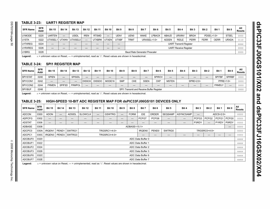
dsPIC33FJ06G
S101/X02 and dsPIC33FJ16G
SX02/X04
DS
70318A-page 50
© 2008 M
icrochip Technology Inc.
Bit 3 Bit 2 Bit 1 Bit 0 All Resets
BRGH PDSEL<1:0> STSEL 0000
PERR FERR OERR URXDA 0110
egister xxxx
egister 0000
0000
Bit 3 Bit 2 Bit 1 Bit 0 All Resets
— — SPITBF SPIRBF 0000
SPRE<2:0> PPRE<1:0> 0000
— — FRMDLY — 0000
0000
t 4 Bit 3 Bit 2 Bit 1 Bit 0 All Resets
SAMP — ADCS<2:0> 0000
PCFG3 PCFG2 PCFG1 PCFG0 0000
P3RDY — P1RDY P0RDY 0000
— 0000
TRGSRC0<4:0> 0000
— — — — 0000
xxxx
xxxx
xxxx
xxxx
xxxx
xxxx
TABLE 3-23: UART1 REGISTER MAP
TABLE 3-24: SPI1 REGISTER MAP
TABLE 3-25: HIGH-SPEED 10-BIT ADC REGISTER MAP FOR dsPIC33FJ06GS101 DEVICES ONLY
SFR Name SFR Addr Bit 15 Bit 14 Bit 13 Bit 12 Bit 11 Bit 10 Bit 9 Bit 8 Bit 7 Bit 6 Bit 5 Bit 4
U1MODE 0220 UARTEN — USIDL IREN RTSMD — UEN1 UEN0 WAKE LPBACK ABAUD URXINV
U1STA 0222 UTXISEL1 UTXINV UTXISEL0 — UTXBRK UTXEN UTXBF TRMT URXISEL<1:0> ADDEN RIDLE
U1TXREG 0224 — — — — — — — UART Transmit R
U1RXREG 0226 — — — — — — — UART Receive R
U1BRG 0228 Baud Rate Generator Prescaler
Legend: x = unknown value on Reset, — = unimplemented, read as ‘0’. Reset values are shown in hexadecimal.
SFR Name SFR Addr Bit 15 Bit 14 Bit 13 Bit 12 Bit 11 Bit 10 Bit 9 Bit 8 Bit 7 Bit 6 Bit 5 Bit 4
SPI1STAT 0240 SPIEN — SPISIDL — — — — — — SPIROV — —
SPI1CON1 0242 — — — DISSCK DISSDO MODE16 SMP CKE SSEN CKP MSTEN
SPI1CON2 0244 FRMEN SPIFSD FRMPOL — — — — — — — — —
SPI1BUF 0248 SPI1 Transmit and Receive Buffer Register
Legend: x = unknown value on Reset, — = unimplemented, read as ‘0’. Reset values are shown in hexadecimal.
SFR Name SFR Addr Bit 15 Bit 14 Bit 13 Bit 12 Bit 11 Bit 10 Bit 9 Bit 8 Bit 7 Bit 6 Bit 5 Bi
ADCON 0300 ADON — ADSIDL SLOWCLK — GSWTRG — FORM EIE ORDER SEQSAMP ASYNC
ADPCFG 0302 — — — — — — — — PCFG7 PCFG6 — —
ADSTAT 0306 — — — — — — — — — — — —
ADBASE 0308 ADBASE<15:1>
ADCPC0 030A IRQEN1 PEND1 SWTRG1 TRGSRC1<4:0> IRQEN0 PEND0 SWTRG0
ADCPC1 030C IRQEN3 PEND3 SWTRG3 TRGSRC3<4:0> — — — —
ADCBUF0 0320 ADC Data Buffer 0
ADCBUF1 0322 ADC Data Buffer 1
ADCBUF2 0324 ADC Data Buffer 2
ADCBUF3 0326 ADC Data Buffer 3
ADCBUF6 032C ADC Data Buffer 6
ADCBUF7 032E ADC Data Buffer 7
Legend: x = unknown value on Reset, — = unimplemented, read as ‘0’. Reset values are shown in hexadecimal.

© 2008 M
icrochip Technology Inc.D
S70318A
-page 51
dsPIC33FJ06G
S101/X02 and dsPIC33FJ16G
SX02/X04
TA
TA
SF Bit 3 Bit 2 Bit 1 Bit 0 All Resets
AD P — ADCS<2:0> 0000
AD PCFG3 PCFG2 PCFG1 PCFG0 0000
AD — P2RDY P1RDY P0RDY 0000
AD — 0000
AD TRGSRC0<4:0> 0000
AD TRGSRC2<4:0> 0000
AD xxxx
AD xxxx
AD xxxx
AD xxxx
AD xxxx
AD xxxx
Le
SF Bit 3 Bit 2 Bit 1 Bit 0 All Resets
AD P — ADCS<2:0> 0000
AD PCFG3 PCFG2 PCFG1 PCFG0 0000
AD — P2RDY P1RDY P0RDY 0000
AD — 0000
AD TRGSRC0<4:0> 0000
AD TRGSRC2<4:0> 0000
AD TRGSRC6<4:0> 0000
AD xxxx
AD xxxx
AD xxxx
AD xxxx
AD xxxx
AD xxxx
AD xxxx
AD xxxx
Le
BLE 3-26: HIGH-SPEED 10-BIT ADC REGISTER MAP FOR dsPIC33FJ06GS102 DEVICES ONLY
BLE 3-27: HIGH-SPEED 10-BIT ADC REGISTER MAP FOR dsPIC33FJ06GS202 DEVICES ONLY
R Name SFR Addr Bit 15 Bit 14 Bit 13 Bit 12 Bit 11 Bit 10 Bit 9 Bit 8 Bit 7 Bit 6 Bit 5 Bit 4
CON 0300 ADON — ADSIDL SLOWCLK — GSWTRG — FORM EIE ORDER SEQSAMP ASYNCSAMPCFG 0302 — — — — — — — — — — PCFG5 PCFG4STAT 0306 — — — — — — — — — — — —BASE 0308 ADBASE<15:1>CPC0 030A IRQEN1 PEND1 SWTRG1 TRGSRC1<4:0> IRQEN0 PEND0 SWTRG0CPC1 030C — — — — — — — — IRQEN2 PEND2 SWTRG2CBUF0 0320 ADC Data Buffer 0CBUF1 0322 ADC Data Buffer 1CBUF2 0324 ADC Data Buffer 2CBUF3 0326 ADC Data Buffer 3CBUF4 0328 ADC Data Buffer 4CBUF5 032A ADC Data Buffer 5gend: x = unknown value on Reset, — = unimplemented, read as ‘0’. Reset values are shown in hexadecimal.
R Name SFR Addr Bit 15 Bit 14 Bit 13 Bit 12 Bit 11 Bit 10 Bit 9 Bit 8 Bit 7 Bit 6 Bit 5 Bit 4
CON 0300 ADON — ADSIDL SLOWCLK — GSWTRG — FORM EIE ORDER SEQSAMP ASYNCSAMPCFG 0302 — — — — — — — — — — PCFG5 PCFG4STAT 0306 — — — — — — — — — P6RDY — —BASE 0308 ADBASE<15:1>CPC0 030A IRQEN1 PEND1 SWTRG1 TRGSRC1<4:0> IRQEN0 PEND0 SWTRG0CPC1 030C — — — — — — — — IRQEN2 PEND2 SWTRG2CPC3 0310 — — — — — — — — IRQEN6 PEND6 SWTRG6CBUF0 0320 ADC Data Buffer 0CBUF1 0322 ADC Data Buffer 1CBUF2 0324 ADC Data Buffer 2CBUF3 0326 ADC Data Buffer 3CBUF4 0328 ADC Data Buffer 4CBUF5 032A ADC Data Buffer 5CBUF12 0338 ADC Data Buffer 12CBUF13 033A ADC Data Buffer13gend: x = unknown value on Reset, — = unimplemented, read as ‘0’. Reset values are shown in hexadecimal.

dsPIC33FJ06G
S101/X02 and dsPIC33FJ16G
SX02/X04
DS
70318A-page 52
© 2008 M
icrochip Technology Inc.
Y
t 4 Bit 3 Bit 2 Bit 1 Bit 0 All Resets
SAMP — ADCS<2:0> 0000
FG4 PCFG3 PCFG2 PCFG1 PCFG0 0000
P3RDY P2RDY P1RDY P0RDY 0000
— 0000
TRGSRC0<4:0> 0000
TRGSRC2<4:0> 0000
xxxx
xxxx
xxxx
xxxx
xxxx
xxxx
xxxx
xxxx
TABLE 3-28: HIGH-SPEED 10-BIT ADC REGISTER MAP FOR dsPIC33FJ16GS402/404 DEVICES ONL
SFR Name SFR Addr Bit 15 Bit 14 Bit 13 Bit 12 Bit 11 Bit 10 Bit 9 Bit 8 Bit 7 Bit 6 Bit 5 Bi
ADCON 0300 ADON — ADSIDL SLOWCLK — GSWTRG — FORM EIE ORDER SEQSAMP ASYNCADPCFG 0302 — — — — — — — — PCFG7 PCFG6 PCFG5 PCADSTAT 0306 — — — — — — — — — — — —ADBASE 0308 ADBASE<15:1>ADCPC0 030A IRQEN1 PEND1 SWTRG1 TRGSRC1<4:0> IRQEN0 PEND0 SWTRG0ADCPC1 030C IRQEN3 PEND3 SWTRG3 TRGSRC3<4:0> IRQEN2 PEND2 SWTRG2ADCBUF0 0320 ADC Data Buffer 0ADCBUF1 0322 ADC Data Buffer 1ADCBUF2 0324 ADC Data Buffer 2ADCBUF3 0326 ADC Data Buffer 3ADCBUF4 0328 ADC Data Buffer 4ADCBUF5 032A ADC Data Buffer 5ADCBUF6 032C ADC Data Buffer 6ADCBUF7 032E ADC Data Buffer 7Legend: x = unknown value on Reset, — = unimplemented, read as ‘0’. Reset values are shown in hexadecimal.

© 2008 M
icrochip Technology Inc.D
S70318A
-page 53
dsPIC33FJ06G
S101/X02 and dsPIC33FJ16G
SX02/X04
TA
SF Bit 3 Bit 2 Bit 1 Bit 0 All Resets
AD P — ADCS<2:0> 0000
AD PCFG3 PCFG2 PCFG1 PCFG0 0000
AD P3RDY P2RDY P1RDY P0RDY 0000
AD — 0000
AD TRGSRC0<4:0> 0000
AD TRGSRC2<4:0> 0000
AD TRGSRC6<4:0> 0000
AD xxxx
AD xxxx
AD xxxx
AD xxxx
AD xxxx
AD xxxx
AD xxxx
AD xxxx
AD xxxx
AD xxxx
Le
BLE 3-29: HIGH-SPEED 10-BIT ADC REGISTER MAP FOR dsPIC33FJ16GS502 DEVICES ONLY
R Name SFR Addr Bit 15 Bit 14 Bit 13 Bit 12 Bit 11 Bit 10 Bit 9 Bit 8 Bit 7 Bit 6 Bit 5 Bit 4
CON 0300 ADON — ADSIDL SLOWCLK — GSWTRG — FORM EIE ORDER SEQSAMP ASYNCSAMPCFG 0302 — — — — — — — — PCFG7 PCFG6 PCFG5 PCFG4STAT 0306 — — — — — — — — — P6RDY — —BASE 0308 ADBASE<15:1>CPC0 030A IRQEN1 PEND1 SWTRG1 TRGSRC1<4:0> IRQEN0 PEND0 SWTRG0CPC1 030C IRQEN3 PEND3 SWTRG3 TRGSRC3<4:0> IRQEN2 PEND2 SWTRG2CPC3 0310 — — — — — — — — IRQEN6 PEND6 SWTRG6CBUF0 0320 ADC Data Buffer 0CBUF1 0322 ADC Data Buffer 1CBUF2 0324 ADC Data Buffer 2CBUF3 0326 ADC Data Buffer 3CBUF4 0328 ADC Data Buffer 4CBUF5 032A ADC Data Buffer 5CBUF6 032C ADC Data Buffer 6CBUF7 032E ADC Data Buffer 7CBUF12 0338 ADC Data Buffer 12CBUF13 033A ADC Data Buffer 13gend: x = unknown value on Reset, — = unimplemented, read as ‘0’. Reset values are shown in hexadecimal.

dsPIC33FJ06G
S101/X02 and dsPIC33FJ16G
SX02/X04
DS
70318A-page 54
© 2008 M
icrochip Technology Inc.
t 4 Bit 3 Bit 2 Bit 1 Bit 0 All Resets
SAMP — ADCS<2:0> 0000
FG4 PCFG3 PCFG2 PCFG1 PCFG0 0000
DY P3RDY P2RDY P1RDY P0RDY 0000
— 0000
TRGSRC0<4:0> 0000
TRGSRC2<4:0> 0000
TRGSRC4<4:0> 0000
TRGSRC6<4:0> 0000
xxxx
xxxx
xxxx
xxxx
xxxx
xxxx
xxxx
xxxx
xxxx
xxxx
xxxx
xxxx
xxxx
xxxx
TABLE 3-30: HIGH-SPEED 10-BIT ADC REGISTER MAP FOR dsPIC33FJ16GS504 DEVICES ONLY
SFR Name SFR Addr Bit 15 Bit 14 Bit 13 Bit 12 Bit 11 Bit 10 Bit 9 Bit 8 Bit 7 Bit 6 Bit 5 Bi
ADCON 0300 ADON — ADSIDL SLOWCLK — GSWTRG — FORM EIE ORDER SEQSAMP ASYNC
ADPCFG 0302 — — — — PCFG11 PCFG10 PCFG9 PCFG8 PCFG7 PCFG6 PCFG5 PC
ADSTAT 0306 — — — — — — — — — P6RDY P5RDY P4R
ADBASE 0308 ADBASE<15:1>
ADCPC0 030A IRQEN1 PEND1 SWTRG1 TRGSRC1<4:0> IRQEN0 PEND0 SWTRG0
ADCPC1 030C IRQEN3 PEND3 SWTRG3 TRGSRC3<4:0> IRQEN2 PEND2 SWTRG2
ADCPC2 030E IRQEN5 PEND5 SWTRG5 TRGSRC5<4:0> IRQEN4 PEND4 SWTRG4
ADCPC3 0310 — — — — — — — — IRQEN6 PEND6 SWTRG6
ADCBUF0 0320 ADC Data Buffer 0
ADCBUF1 0322 ADC Data Buffer 1
ADCBUF2 0324 ADC Data Buffer 2
ADCBUF3 0326 ADC Data Buffer 3
ADCBUF4 0328 ADC Data Buffer 4
ADCBUF5 032A ADC Data Buffer 5
ADCBUF6 032C ADC Data Buffer 6
ADCBUF7 032E ADC Data Buffer 7
ADCBUF8 0330 ADC Data Buffer 8
ADCBUF9 0332 ADC Data Buffer 9
ADCBUF10 0334 ADC Data Buffer 10
ADCBUF11 0336 ADC Data Buffer 11
ADCBUF12 0338 ADC Data Buffer 12
ADCBUF13 033A ADC Data Buffer 13
Legend: x = unknown value on Reset, — = unimplemented, read as ‘0’. Reset values are shown in hexadecimal.

© 2008 M
icrochip Technology Inc.D
S70318A
-page 55
dsPIC33FJ06G
S101/X02 and dsPIC33FJ16G
SX02/X04
TA NLY
TA LY
Fi Bit 3 Bit 2 Bit 1 Bit 0 All Resets
CM PSTAT — CMPPOL RANGE 0000
CM 0000
CM PSTAT — CMPPOL RANGE 0000
CM 0000
Fi Bit 3 Bit 2 Bit 1 Bit 0 All Resets
CM PSTAT — CMPPOL RANGE 0000
CM 0000
CM PSTAT — CMPPOL RANGE 0000
CM 0000
CM PSTAT — CMPPOL RANGE 0000
CM 0000
CM PSTAT — CMPPOL RANGE 0000
CM 0000
BLE 3-31: ANALOG COMPARATOR CONTROL REGISTER MAP FOR dsPIC33FJ06GS202 DEVICES O
BLE 3-32: ANALOG COMPARATOR CONTROL REGISTER MAP dsPIC33FJ16GS502/504 DEVICES ON
le Name ADR Bit 15 Bit 14 Bit 13 Bit 12 Bit 11 Bit 10 Bit 9 Bit 8 Bit 7 Bit 6 Bit 5 Bit 4
PCON1 0540 CMPON — CMPSIDL — — — — DACOE INSEL<1:0> EXTREF — CM
PDAC1 0542 — — — — — — CMREF<9:0>
PCON2 0544 CMPON — CMPSIDL — — — — DACOE INSEL<1:0> EXTREF — CM
PDAC2 0546 — — — — — — CMREF<9:0>
le Name ADR Bit 15 Bit 14 Bit 13 Bit 12 Bit 11 Bit 10 Bit 9 Bit 8 Bit 7 Bit 6 Bit 5 Bit 4
PCON1 0540 CMPON — CMPSIDL — — — — DACOE INSEL<1:0> EXTREF — CM
PDAC1 0542 — — - — — — CMREF<9:0>
PCON2 0544 CMPON — CMPSIDL — — — — DACOE INSEL<1:0> EXTREF — CM
PDAC2 0546 — — - — — — CMREF<9:0>
PCON3 0548 CMPON — CMPSIDL — — — — DACOE INSEL<1:0> EXTREF — CM
PDAC3 054A — — - — — — CMREF<9:0>
PCON4 054C CMPON — CMPSIDL — — — — DACOE INSEL<1:0> EXTREF — CM
PDAC4 054E — — — — — — CMREF<9:0>

dsPIC33FJ06G
S101/X02 and dsPIC33FJ16G
SX02/X04
DS
70318A-page 56
© 2008 M
icrochip Technology Inc.
Bit 3 Bit 2 Bit 1 Bit 0 All Resets
— — — — 3F00
INT2R<5:0> 003F
— — — — 0000
T2CKR<5:0> 3F3F
IC1R<5:0> 3F3F
OCFAR<5:0> 3F3F
U1RXR<5:0> 003F
SDI1R<5:0> 3F3F
SS1R<5:0> 0000
— — — — 3F00
FLT2R<5:0> 3F3F
FLT4R<5:0> 3F3F
FLT6R<5:0> 3F3F
FLT8R<5:0> 3F3F
SYNCI2R<5:0> 3F3F
Bit 3 Bit 2 Bit 1 Bit 0 All Resets
RP0R<5:0> 0000
RP2R<5:0> 0000
RP4R<5:0> 0000
RP6R<5:0> 0000
TABLE 3-33: PERIPHERAL PIN SELECT INPUT REGISTER MAP
TABLE 3-34: PERIPHERAL PIN SELECT OUTPUT REGISTER MAP FOR dsPIC33FJ06GS101
SFR Name SFR Addr Bit 15 Bit 14 Bit 13 Bit 12 Bit 11 Bit 10 Bit 9 Bit 8 Bit 7 Bit 6 Bit 5 Bit 4
RPINR0 0680 — — INT1R<5:0> — — — —
RPINR1 0682 — — — — — — — — — —
RPINR2 0684 — — T1CKR<5:0> — — — —
RPINR3 0686 — — T3CKR<5:0> — —
RPINR7 068E — — IC2R<5:0> — —
RPINR11 0696 — — — — — — — — — —
RPINR18 06A4 — — U1CTSR<5:0> — —
RPINR20 06A8 — — SCK1R<5:0> — —
RPINR21 06AA — — — — — — — — — —
RPINR29 06BA — — FLT1R<5:0> — — — —
RPINR30 06BC — — FLT3R<5:0> — —
RPINR31 06BE — — FLT5R<5:0> — —
RPINR32 06C0 — — FLT7R<5:0> — —
RPINR33 06C2 — — SYNCI1R<5:0> — —
RPINR34 06C4 — — — — — — — — — —
Legend: x = unknown value on Reset, — = unimplemented, read as ‘0’. Reset values are shown in hexadecimal.
File Name Addr Bit 15 Bit 14 Bit 13 Bit 12 Bit 11 Bit 10 Bit 9 Bit 8 Bit 7 Bit 6 Bit 5 Bit 4
RPOR0 06D0 — — RP1R<5:0> — —RPOR1 06D2 — — RP3R<5:0> — —
RPOR2 06D4 — — RP5R<5:0> — —
RPOR3 06D6 — — RP7R<5:0> — —
Legend: x = unknown value on Reset, — = unimplemented, read as ‘0’. Reset values are shown in hexadecimal.

© 2008 M
icrochip Technology Inc.D
S70318A
-page 57
dsPIC33FJ06G
S101/X02 and dsPIC33FJ16G
SX02/X04
TA 06GS202, dsPIC33FJ16GS402
TA 33FJ16GS504
Fi Bit 3 Bit 2 Bit 1 Bit 0 All Resets
RP RP0R<5:0> 0000
RP RP2R<5:0> 0000
RP RP4R<5:0> 0000
RP RP6R<5:0> 0000
RP RP8R<5:0> 0000
RP RP10R<5:0> 0000
RP RP12R<5:0> 0000
RP RP14R<5:0> 0000
Le
Fi Bit 3 Bit 2 Bit 1 Bit 0 All Resets
RP RP0R<5:0> 0000
RP RP2R<5:0> 0000
RP RP4R<5:0> 0000
RP RP6R<5:0> 0000
RP RP8R<5:0> 0000
RP RP10R<5:0> 0000
RP RP12R<5:0> 0000
RP RP14R<5:0> 0000
RP RP16R<5:0> 0000
RP RP18R<5:0> 0000
RP RP20R<5:0> 0000
RP RP22R<5:0> 0000
RP RP24R<5:0> 0000
RP RP26R<5:0> 0000
RP RP28R<5:0> 0000
Le
BLE 3-35: PERIPHERAL PIN SELECT OUTPUT REGISTER MAP FOR dsPIC33FJ06GS102, dsPIC33FJAND dsPIC33FJ16GS502
BLE 3-36: PERIPHERAL PIN SELECT OUTPUT REGISTER MAP FOR dsPIC33FJ16GS404 AND dsPIC
le Name Addr Bit 15 Bit 14 Bit 13 Bit 12 Bit 11 Bit 10 Bit 9 Bit 8 Bit 7 Bit 6 Bit 5 Bit 4
OR0 06D0 — — RP1R<5:0> — —OR1 06D2 — — RP3R<5:0> — —OR2 06D4 — — RP5R<5:0> — —OR3 06D6 — — RP7R<5:0> — —OR4 06D8 — — RP9R<5:0> — —OR5 06DA — — RP11R<5:0> — —OR6 06DC — — RP13R<5:0> — —OR7 06DE — — RP15R<5:0> — —gend: x = unknown value on Reset, — = unimplemented, read as ‘0’. Reset values are shown in hexadecimal.
le Name Addr Bit 15 Bit 14 Bit 13 Bit 12 Bit 11 Bit 10 Bit 9 Bit 8 Bit 7 Bit 6 Bit 5 Bit 4
OR0 06D0 — — RP1R<5:0> — —OR1 06D2 — — RP3R<5:0> — —OR2 06D4 — — RP5R<5:0> — —OR3 06D6 — — RP7R<5:0> — —OR4 06D8 — — RP9R<5:0> — —OR5 06DA — — RP11R<5:0> — —OR6 06DC — — RP13R<5:0> — —OR7 06DE — — RP15R<5:0> — —OR8 06E0 — — RP17R<5:0> — —OR9 06E2 — — RP19R<5:0> — —OR10 06E4 — — RP21R<5:0> — —OR11 06E6 — — RP23R<5:0> — —OR12 06E8 — — RP25R<5:0> — —OR13 06EA — — RP27R<5:0> — —OR14 06EC — — RP29R<5:0> — —gend: x = unknown value on Reset, — = unimplemented, read as ‘0’. Reset values are shown in hexadecimal.

dsPIC33FJ06G
S101/X02 and dsPIC33FJ16G
SX02/X04
DS
70318A-page 58
© 2008 M
icrochip Technology Inc.
S402, dsPIC33FJ16GS404,
Bit 3 Bit 2 Bit 1 Bit 0 All Resets
TRISA3 TRISA2 TRISA1 TRISA0 001F
RA3 RA2 RA1 RA0 xxxx
LATA3 LATA2 LATA1 LATA0 0000
ODCA3 — — — 0000
Bit 3 Bit 2 Bit 1 Bit 0 All Resets
TRISB3 TRISB2 TRISB1 TRISB0 00FF
RB3 RB2 RB1 RB0 xxxx
LATB3 LATB2 LATB1 LATB0 0000
— — — — 0000
4 Bit 3 Bit 2 Bit 1 Bit 0 All Resets
B4 TRISB3 TRISB2 TRISB1 TRISB0 FFFF
4 RB3 RB2 RB1 RB0 xxxx
B4 LATB3 LATB2 LATB1 LATB0 0000
— — — — 0000
Bit 3 Bit 2 Bit 1 Bit 0 All Resets
TRISC3 TRISC2 TRISC1 TRISC0 3FFF
RC3 RC2 RC1 RC0 xxxx
LATC3 LATC2 LATC1 LATC0 0000
ODCC3 — — ODCC0 0000
TABLE 3-37: PORTA REGISTER MAP
TABLE 3-38: PORTB REGISTER MAP FOR dsPIC33FJ06GS101
TABLE 3-39: PORTB REGISTER MAP FOR dsPIC33FJ06GS102, dsPIC33FJ06GS202, dsPIC33FJ16GdsPIC33FJ16GS502 and dsPIC33FJ16GS504
TABLE 3-40: PORTC REGISTER MAP FOR dsPIC33FJ16GS404 and dsPIC33FJ16GS504
SFR Name SFR Addr Bit 15 Bit 14 Bit 13 Bit 12 Bit 11 Bit 10 Bit 9 Bit 8 Bit 7 Bit 6 Bit 5 Bit 4
TRISA 02C0 — — — — — — — — — — — TRISA4
PORTA 02C2 — — — — — — — — — — — RA4
LATA 02C4 — — — — — — — — — — — LATA4
ODCA 02C6 — — — — — — — — — — — ODCA4
Legend: x = unknown value on Reset, — = unimplemented, read as ‘0’. Reset values are shown in hexadecimal.
SFR Name SFR Addr Bit 15 Bit 14 Bit 13 Bit 12 Bit 11 Bit 10 Bit 9 Bit 8 Bit 7 Bit 6 Bit 5 Bit 4
TRISB 02C8 — — — — — — — — TRISB7 TRISB6 TRISB5 TRISB4
PORTB 02CA — — — — — — — — RB7 RB6 RB5 RB4
LATB 02CC — — — — — — — — LATB7 LATB6 LATB5 LATB4
ODCB 02CE — — — — — — — — ODCB7 ODCB6 — —
Legend: x = unknown value on Reset, — = unimplemented, read as ‘0’. Reset values are shown in hexadecimal.
SFR Name
SFR Addr Bit 15 Bit 14 Bit 13 Bit 12 Bit 11 Bit 10 Bit 9 Bit 8 Bit 7 Bit 6 Bit 5 Bit
TRISB 02C8 TRISB15 TRISB14 TRISB13 TRISB12 TRISB11 TRISB10 TRISB9 TRISB8 TRISB7 TRISB6 TRISB5 TRIS
PORTB 02CA RB15 RB14 RB13 RB12 RB11 RB10 RB9 RB8 RB7 RB6 RB5 RB
LATB 02CC LATB15 LATB14 LATB13 LATB12 LATB11 LATB10 LATB9 LATB8 LATB7 LATB6 LATB5 LAT
ODCB 02CE ODCB15 ODCB14 ODCB13 ODCB12 ODCB11 — — ODCB8 ODCB7 ODCB6 — —
Legend: x = unknown value on Reset, — = unimplemented, read as ‘0’. Reset values are shown in hexadecimal.
SFR Name SFR Addr Bit 15 Bit 14 Bit 13 Bit 12 Bit 11 Bit 10 Bit 9 Bit 8 Bit 7 Bit 6 Bit 5 Bit 4
TRISC 02D0 — — TRISC13 TRISC12 TRISC11 TRISC10 TRISC9 TRISC8 TRISC7 TRISC6 TRISC5 TRISC4
PORTC 02D2 — — RC13 RC12 RC11 RC10 RC9 RC8 RC7 RC6 RC5 RC4
LATC 02D4 — — LATC13 LATC12 LATC11 LATC10 LATC9 LATC8 LATC7 LATC6 LATC5 LATC4
ODCC 02D6 — — ODCC13 ODCC12 ODCC11 — — ODCC8 ODCC7 ODCC6 ODCC5 ODCC4
Legend: x = unknown value on Reset, — = unimplemented, read as ‘0’. Reset values are shown in hexadecimal.

© 2008 M
icrochip Technology Inc.D
S70318A
-page 59
dsPIC33FJ06G
S101/X02 and dsPIC33FJ16G
SX02/X04
TA
TA
TA
S it 3 Bit 2 Bit 1 Bit 0 All Resets
RC LEEP IDLE BOR POR xxxx(1)
OS CF — — OSWEN 0300(2)
CL PLLPRE<4:0> 0040
PL 0030
RE — — — — 0000
OS TUN<5:0> 0000
AC — — — — 0000
LeNo
Fi Bit 3 Bit 2 Bit 1 Bit 0 All Resets
NV NVMOP<3:0> 0000(1)
NV :0> 0000
LeNo t.
N Bit 3 Bit 2 Bit 1 Bit 0 All Resets
PM SPI1MD — — ADCMD 0000
PM — — OC2MD OC1MD 0000
PM — — — — 0000
PM REFOMD — — — 0000
PM — — — — 0000
PM — — — — 0000
Le
BLE 3-41: SYSTEM CONTROL REGISTER MAP
BLE 3-42: NVM REGISTER MAP
BLE 3-43: PMD REGISTER MAP
FR Name SFR Addr Bit 15 Bit 14 Bit 13 Bit 12 Bit 11 Bit 10 Bit 9 Bit 8 Bit 7 Bit 6 Bit 5 Bit 4 B
ON 0740 TRAPR IOPUWR — — — — CM VREGS EXTR SWR SWDTEN WDTO S
CCON 0742 — COSC<2:0> — NOSC<2:0> CLKLOCK IOLOCK LOCK —
KDIV 0744 ROI DOZEN<2:0> DOZN FRCDIV<2:0> PLLPOST<1:0> —
LFBD 0746 — — — — — — — PLLDIV<8:0>
FOCON 074E ROON — ROSIDL ROSEL RODIV<3:0> — — — —
CTUN 0748
LKCON 0750 ENAPLL APLLCK SELACLK — — APSTSCLR<2:0> ASRCSEL FRCSEL — —
gend: x = unknown value on Reset, — = unimplemented, read as ‘0’. Reset values are shown in hexadecimal.te 1: The RCON register reset values are dependent on type of reset.
2: The OSCCON register reset values are dependent on the FOSC configuration bits, and on type of reset.
le Name Addr Bit 15 Bit 14 Bit 13 Bit 12 Bit 11 Bit 10 Bit 9 Bit 8 Bit 7 Bit 6 Bit 5 Bit 4
MCON 0760 WR WREN WRERR — — — — — — ERASE — —
MKEY 0766 — — — — — — — — NVMKEY<7
gend: x = unknown value on Reset, — = unimplemented, read as ‘0’. Reset values are shown in hexadecimal.te 1: Reset value shown is for POR only. Value on other Reset states is dependent on the state of memory write or erase operations at the time of Rese
SFR ame
SFR Addr Bit 15 Bit 14 Bit 13 Bit 12 Bit 11 Bit 10 Bit 9 Bit 8 Bit 7 Bit 6 Bit 5 Bit 4
D1 0770 — — T3MD T2MD T1MD — PWMMD — I2C1MD — U1MD —
D2 0772 — — — — — — IC2MD IC1MD — — — —
D3 0774 — — — — — CMPMD — — — — — —
D4 0776 — — — — — — — — — — — —
D6 077A — — — — PWM4MD PWM3MD PWM2MD PWM1MD — — — —
D7 077C — — — — CMP4MD CMP3MD CMP2MD CMP1MD — — — —
gend: x = unknown value on Reset, — = unimplemented, read as ‘0’. Reset values are shown in hexadecimal.

dsPIC33FJ06GS101/X02 and dsPIC33FJ16GSX02/X04
3.2.6 SOFTWARE STACK
In addition to its use as a working register, the W15register in the dsPIC33FJ06GS101/X02 anddsPIC33FJ16GSX02/X04 devices is also used as asoftware Stack Pointer. The Stack Pointer alwayspoints to the first available free word and grows fromlower to higher addresses. It predecrements for stackpops and post-increments for stack pushes, as shownin Figure 3-6. For a PC push during any CALL instruc-tion, the MSb of the PC is zero-extended before thepush, ensuring that the MSb is always clear.
The Stack Pointer Limit register (SPLIM) associatedwith the Stack Pointer sets an upper address boundaryfor the stack. SPLIM is uninitialized at Reset. As is thecase for the Stack Pointer, SPLIM<0> is forced to ‘0’because all stack operations must be word-aligned.
Whenever an EA is generated using W15 as a sourceor destination pointer, the resulting address iscompared with the value in SPLIM. If the contents ofthe Stack Pointer (W15) and the SPLIM register areequal and a push operation is performed, a stack errortrap will not occur. The stack error trap will occur on asubsequent push operation. For example, to cause astack error trap when the stack grows beyond address0x2000 in RAM, initialize the SPLIM with the value0x1FFE.
Similarly, a Stack Pointer underflow (stack error) trap isgenerated when the Stack Pointer address is found tobe less than 0x0800. This prevents the stack frominterfering with the Special Function Register (SFR)space.
A write to the SPLIM register should not be immediatelyfollowed by an indirect read operation using W15.
FIGURE 3-6: CALL STACK FRAME
3.2.7 DATA RAM PROTECTION FEATUREThe dsPIC33F product family supports Data RAMprotection features that enable segments of RAM to beprotected when used in conjunction with Boot andSecure Code Segment Security. BSRAM (Secure RAMsegment for BS) is accessible only from the BootSegment Flash code when enabled. SSRAM (SecureRAM segment for RAM) is accessible only from theSecure Segment Flash code when enabled. SeeTable 3-1 for an overview of the BSRAM and SSRAMSFRs.
3.3 Instruction Addressing ModesThe addressing modes shown in Table 3-44 form thebasis of the addressing modes optimized to support thespecific features of individual instructions. Theaddressing modes provided in the MAC class ofinstructions differ from those in the other instructiontypes.
3.3.1 FILE REGISTER INSTRUCTIONSMost file register instructions use a 13-bit address field(f) to directly address data present in the first 8192bytes of data memory (near data space). Most fileregister instructions employ a working register, W0,which is denoted as WREG in these instructions. Thedestination is typically either the same file register orWREG (with the exception of the MUL instruction),which writes the result to a register or register pair. TheMOV instruction allows additional flexibility and canaccess the entire data space.
3.3.2 MCU INSTRUCTIONSThe three-operand MCU instructions are of the form:
Operand 3 = Operand 1 <function> Operand 2
where Operand 1 is always a working register (that is,the addressing mode can only be register direct), whichis referred to as Wb. Operand 2 can be a W register,fetched from data memory, or a 5-bit literal. The resultlocation can be either a W register or a data memorylocation. The following addressing modes aresupported by MCU instructions:
• Register Direct• Register Indirect• Register Indirect Post-Modified• Register Indirect Pre-Modified• 5-bit or 10-bit Literal
Note: A PC push during exception processingconcatenates the SRL register to the MSbof the PC prior to the push.
<Free Word>
PC<15:0>000000000
015
W15 (before CALL)
W15 (after CALL)
Stac
k G
row
s To
war
dH
ighe
r Add
ress
0x0000
PC<22:16>
POP : [--W15]PUSH : [W15++]
Note: Not all instructions support all theaddressing modes given above. Individualinstructions can support different subsetsof these addressing modes.
DS70318A-page 60 © 2008 Microchip Technology Inc.

dsPIC33FJ06GS101/X02 and dsPIC33FJ16GSX02/X04
TABLE 3-44: FUNDAMENTAL ADDRESSING MODES SUPPORTED
3.3.3 MOVE AND ACCUMULATOR INSTRUCTIONS
Move instructions and the DSP accumulator class ofinstructions provide a greater degree of addressingflexibility than other instructions. In addition to theaddressing modes supported by most MCUinstructions, move and accumulator instructions alsosupport Register Indirect with Register OffsetAddressing mode, also referred to as Register Indexedmode.
In summary, the following addressing modes aresupported by move and accumulator instructions:
• Register Direct• Register Indirect• Register Indirect Post-modified• Register Indirect Pre-modified• Register Indirect with Register Offset (Indexed)• Register Indirect with Literal Offset• 8-bit Literal• 16-bit Literal
3.3.4 MAC INSTRUCTIONSThe dual source operand DSP instructions (CLR, ED,EDAC, MAC, MPY, MPY.N, MOVSAC and MSC), also referredto as MAC instructions, use a simplified set of addressingmodes to allow the user application to effectivelymanipulate the data pointers through register indirecttables.
The two-source operand prefetch registers must bemembers of the set {W8, W9, W10, W11}. For datareads, W8 and W9 are always directed to the X RAGU,and W10 and W11 are always directed to the Y AGU.The effective addresses generated (before and aftermodification) must, therefore, be valid addresses withinX data space for W8 and W9 and Y data space for W10and W11.
In summary, the following addressing modes aresupported by the MAC class of instructions:
• Register Indirect• Register Indirect Post-Modified by 2• Register Indirect Post-Modified by 4• Register Indirect Post-Modified by 6• Register Indirect with Register Offset (Indexed)
3.3.5 OTHER INSTRUCTIONSBesides the addressing modes outlined previously, someinstructions use literal constants of various sizes. Forexample, BRA (branch) instructions use 16-bit signedliterals to specify the branch destination directly, whereasthe DISI instruction uses a 14-bit unsigned literal field. Insome instructions, such as ADD Acc, the source of anoperand or result is implied by the opcode itself. Certainoperations, such as NOP, do not have any operands.
Addressing Mode Description
File Register Direct The address of the file register is specified explicitly.Register Direct The contents of a register are accessed directly.Register Indirect The contents of Wn forms the Effective Address (EA).Register Indirect Post-Modified The contents of Wn forms the EA. Wn is post-modified (incremented or
decremented) by a constant value.Register Indirect Pre-Modified Wn is pre-modified (incremented or decremented) by a signed constant value
to form the EA.Register Indirect with Register Offset (Register Indexed)
The sum of Wn and Wb forms the EA.
Register Indirect with Literal Offset The sum of Wn and a literal forms the EA.
Note: For the MOV instructions, the addressingmode specified in the instruction can differfor the source and destination EA.However, the 4-bit Wb (Register Offset)field is shared by both source anddestination (but typically only used byone).
Note: Not all instructions support all theaddressing modes given above. Individualinstructions may support different subsetsof these addressing modes.
Note: Register Indirect with Register OffsetAddressing mode is available only for W9(in X space) and W11 (in Y space).
© 2008 Microchip Technology Inc. DS70318A-page 61

dsPIC33FJ06GS101/X02 and dsPIC33FJ16GSX02/X04
3.4 Modulo AddressingModulo Addressing mode is a method used to providean automated means to support circular data buffersusing hardware. The objective is to remove the needfor software to perform data address boundary checkswhen executing tightly looped code, as is typical inmany DSP algorithms.
Modulo Addressing can operate in either data or programspace (since the data pointer mechanism is essentiallythe same for both). One circular buffer can be supportedin each of the X (which also provides the pointers intoprogram space) and Y data spaces. Modulo Addressingcan operate on any W register pointer. However, it is notadvisable to use W14 or W15 for Modulo Addressingsince these two registers are used as the Stack FramePointer and Stack Pointer, respectively.
In general, any particular circular buffer can beconfigured to operate in only one direction as there arecertain restrictions on the buffer start address (forincrementing buffers), or end address (fordecrementing buffers), based upon the direction of thebuffer.
The only exception to the usage restrictions is forbuffers that have a power-of-two length. As thesebuffers satisfy the start and end address criteria, theycan operate in a bidirectional mode (that is, addressboundary checks are performed on both the lower andupper address boundaries).
3.4.1 START AND END ADDRESSThe Modulo Addressing scheme requires that astarting and ending address be specified and loadedinto the 16-bit Modulo Buffer Address registers:XMODSRT, XMODEND, YMODSRT and YMODEND(see Table 3-1).
The length of a circular buffer is not directly specified. Itis determined by the difference between thecorresponding start and end addresses. The maximumpossible length of the circular buffer is 32K words(64 Kbytes).
3.4.2 W ADDRESS REGISTER SELECTION
The Modulo and Bit-Reversed Addressing Controlregister, MODCON<15:0>, contains enable flags aswell as a W register field to specify the W Addressregisters. The XWM and YWM fields select theregisters that will operate with Modulo Addressing:
• If XWM = 15, X RAGU and X WAGU Modulo Addressing is disabled.
• If YWM = 15, Y AGU Modulo Addressing is disabled.
The X Address Space Pointer W register (XWM), towhich Modulo Addressing is to be applied, is stored inMODCON<3:0> (see Table 3-1). Modulo Addressing isenabled for X data space when XWM is set to any valueother than ‘15’ and the XMODEN bit is set atMODCON<15>.
The Y Address Space Pointer W register (YWM) towhich Modulo Addressing is to be applied is stored inMODCON<7:4>. Modulo Addressing is enabled for Ydata space when YWM is set to any value other than‘15’ and the YMODEN bit is set at MODCON<14>.
FIGURE 3-7: MODULO ADDRESSING OPERATION EXAMPLE
Note: Y space Modulo Addressing EAcalculations assume word-sized data (LSbof every EA is always clear).
0x1100
0x1163
Start Addr = 0x1100End Addr = 0x1163Length = 0x0032 words
ByteAddress
MOV #0x1100, W0MOV W0, XMODSRT ;set modulo start addressMOV #0x1163, W0MOV W0, MODEND ;set modulo end addressMOV #0x8001, W0MOV W0, MODCON ;enable W1, X AGU for modulo
MOV #0x0000, W0 ;W0 holds buffer fill value
MOV #0x1110, W1 ;point W1 to buffer
DO AGAIN, #0x31 ;fill the 50 buffer locationsMOV W0, [W1++] ;fill the next locationAGAIN: INC W0, W0 ;increment the fill value
DS70318A-page 62 © 2008 Microchip Technology Inc.

dsPIC33FJ06GS101/X02 and dsPIC33FJ16GSX02/X04
3.4.3 MODULO ADDRESSING APPLICABILITY
Modulo Addressing can be applied to the EffectiveAddress (EA) calculation associated with any Wregister. Address boundaries check for addressesequal to:
• The upper boundary addresses for incrementing buffers
• The lower boundary addresses for decrementing buffers
It is important to realize that the address boundariescheck for addresses less than or greater than the upper(for incrementing buffers) and lower (for decrementingbuffers) boundary addresses (not just equal to).Address changes can, therefore, jump beyondboundaries and still be adjusted correctly.
3.5 Bit-Reversed AddressingBit-Reversed Addressing mode is intended to simplifydata re-ordering for radix-2 FFT algorithms. It issupported by the X AGU for data writes only.
The modifier, which can be a constant value or registercontents, is regarded as having its bit order reversed. Theaddress source and destination are kept in normal order.Thus, the only operand requiring reversal is the modifier.
3.5.1 BIT-REVERSED ADDRESSING IMPLEMENTATION
Bit-Reversed Addressing mode is enabled in any ofthese situations:
• BWM bits (W register selection) in the MODCON register are any value other than ‘15’ (the stack cannot be accessed using Bit-Reversed Addressing)
• The BREN bit is set in the XBREV register• The addressing mode used is Register Indirect
with Pre-Increment or Post-Increment
If the length of a bit-reversed buffer is M = 2N bytes,the last ‘N’ bits of the data buffer start address mustbe zeros.
XB<14:0> is the Bit-Reversed Address modifier, or‘pivot point,’ which is typically a constant. In the case ofan FFT computation, its value is equal to half of the FFTdata buffer size.
When enabled, Bit-Reversed Addressing is executedonly for Register Indirect with Pre-Increment orPost-Increment Addressing and word-sized datawrites. It will not function for any other addressingmode or for byte-sized data, and normal addresses aregenerated instead. When Bit-Reversed Addressing isactive, the W Address Pointer is always added to theaddress modifier (XB), and the offset associated withthe Register Indirect Addressing mode is ignored. Inaddition, as word-sized data is a requirement, the LSbof the EA is ignored (and always clear).
If Bit-Reversed Addressing has already been enabledby setting the BREN (XBREV<15>) bit, a write to theXBREV register should not be immediately followed byan indirect read operation using the W register that hasbeen designated as the bit-reversed pointer.
Note: The modulo corrected effective address iswritten back to the register only whenPre-Modify or Post-Modify Addressingmode is used to compute the effectiveaddress. When an address offset (such as[W7 + W2]) is used, Modulo Addresscorrection is performed but the contents ofthe register remain unchanged.
Note: All bit-reversed EA calculations assumeword-sized data (LSb of every EA isalways clear). The XB value is scaledaccordingly to generate compatible (byte)addresses.
Note: Modulo Addressing and Bit-ReversedAddressing should not be enabledtogether. If an application attempts to do so,Bit-Reversed Addressing will assumepriority when active for the X WAGU and XWAGU, Modulo Addressing will be dis-abled. However, Modulo Addressing willcontinue to function in the X RAGU.
© 2008 Microchip Technology Inc. DS70318A-page 63

dsPIC33FJ06GS101/X02 and dsPIC33FJ16GSX02/X04
FIGURE 3-8: BIT-REVERSED ADDRESS EXAMPLE
TABLE 3-45: BIT-REVERSED ADDRESS SEQUENCE (16-ENTRY)
b3 b2 b1 0
b2 b3 b4 0
Bit Locations Swapped Left-to-RightAround Center of Binary Value
Bit-Reversed Address
XB = 0x0008 for a 16-Word Bit-Reversed Buffer
b7 b6 b5 b1
b7 b6 b5 b4b11 b10 b9 b8
b11 b10 b9 b8
b15 b14 b13 b12
b15 b14 b13 b12
Sequential Address
Pivot Point
Normal Address Bit-Reversed Address
A3 A2 A1 A0 Decimal A3 A2 A1 A0 Decimal
0 0 0 0 0 0 0 0 0 00 0 0 1 1 1 0 0 0 80 0 1 0 2 0 1 0 0 40 0 1 1 3 1 1 0 0 120 1 0 0 4 0 0 1 0 20 1 0 1 5 1 0 1 0 100 1 1 0 6 0 1 1 0 60 1 1 1 7 1 1 1 0 141 0 0 0 8 0 0 0 1 11 0 0 1 9 1 0 0 1 91 0 1 0 10 0 1 0 1 51 0 1 1 11 1 1 0 1 131 1 0 0 12 0 0 1 1 31 1 0 1 13 1 0 1 1 111 1 1 0 14 0 1 1 1 71 1 1 1 15 1 1 1 1 15
DS70318A-page 64 © 2008 Microchip Technology Inc.

dsPIC33FJ06GS101/X02 and dsPIC33FJ16GSX02/X04
3.6 Interfacing Program and Data Memory Spaces
The dsPIC33FJ06GS101/X02 anddsPIC33FJ16GSX02/X04 architecture uses a 24-bit-wideprogram space and a 16-bit-wide data space. Thearchitecture is also a modified Harvard scheme, meaningthat data can also be present in the program space. Touse this data successfully, it must be accessed in a waythat preserves the alignment of information in bothspaces.
Aside from normal execution, thedsPIC33FJ06GS101/X02 anddsPIC33FJ16GSX02/X04 architecture provides twomethods by which program space can be accessedduring operation:
• Using table instructions to access individual bytes or words anywhere in the program space
• Remapping a portion of the program space into the data space (Program Space Visibility)
Table instructions allow an application to read or writeto small areas of the program memory. This capabilitymakes the method ideal for accessing data tables thatneed to be updated periodically. It also allows accessto all bytes of the program word. The remappingmethod allows an application to access a large block ofdata on a read-only basis, which is ideal for look-upsfrom a large table of static data. The application canonly access the least significant word of the programword.
3.6.1 ADDRESSING PROGRAM SPACESince the address ranges for the data and programspaces are 16 and 24 bits, respectively, a method isneeded to create a 23-bit or 24-bit program addressfrom 16-bit data registers. The solution depends on theinterface method to be used.
For table operations, the 8-bit Table Page register(TBLPAG) is used to define a 32K word region withinthe program space. This is concatenated with a 16-bitEA to arrive at a full 24-bit program space address. Inthis format, the Most Significant bit of TBLPAG is usedto determine if the operation occurs in the user memory(TBLPAG<7> = 0) or the configuration memory(TBLPAG<7> = 1).
For remapping operations, the 8-bit Program SpaceVisibility Register (PSVPAG) is used to define a16K word page in the program space. When the MostSignificant bit of the EA is ‘1’, PSVPAG is concatenatedwith the lower 15 bits of the EA to form a 23-bit programspace address. Unlike table operations, this limitsremapping operations strictly to the user memory area.
Table 3-46 and Figure 3-9 show how the program EA iscreated for table operations and remapping accessesfrom the data EA. Here, P<23:0> refers to a programspace word, and D<15:0> refers to a data space word.
TABLE 3-46: PROGRAM SPACE ADDRESS CONSTRUCTION
Access Type AccessSpace
Program Space Address<23> <22:16> <15> <14:1> <0>
Instruction Access(Code Execution)
User 0 PC<22:1> 0
0xx xxxx xxxx xxxx xxxx xxx0
TBLRD/TBLWT(Byte/Word Read/Write)
User TBLPAG<7:0> Data EA<15:0> 0xxx xxxx xxxx xxxx xxxx xxxx
Configuration TBLPAG<7:0> Data EA<15:0> 1xxx xxxx xxxx xxxx xxxx xxxx
Program Space Visibility(Block Remap/Read)
User 0 PSVPAG<7:0> Data EA<14:0>(1)
0 xxxx xxxx xxx xxxx xxxx xxxx
Note 1: Data EA<15> is always ‘1’ in this case, but is not used in calculating the program space address. Bit 15 of the address is PSVPAG<0>.
© 2008 Microchip Technology Inc. DS70318A-page 65

dsPIC33FJ06GS101/X02 and dsPIC33FJ16GSX02/X04
FIGURE 3-9: DATA ACCESS FROM PROGRAM SPACE ADDRESS GENERATION
0Program Counter
23 bits
1
PSVPAG
8 bits
EA
15 bits
Program Counter(1)
Select
TBLPAG
8 bits
EA
16 bits
Byte Select
0
0
1/0
User/Configuration
Table Operations(2)
Program Space Visibility(1)
Space Select
24 bits
23 bits
(Remapping)
1/0
0
Note 1: The Least Significant bit (LSb) of program space addresses is always fixed as ‘0’ to maintain wordalignment of data in the program and data spaces.
2: Table operations are not required to be word-aligned. Table read operations are permitted in theconfiguration memory space.
DS70318A-page 66 © 2008 Microchip Technology Inc.

dsPIC33FJ06GS101/X02 and dsPIC33FJ16GSX02/X04
3.6.2 DATA ACCESS FROM PROGRAM MEMORY USING TABLE INSTRUCTIONS
The TBLRDL and TBLWTL instructions offer a directmethod of reading or writing the lower word of anyaddress within the program space without goingthrough data space. The TBLRDH and TBLWTHinstructions are the only method to read or write theupper 8 bits of a program space word as data.
The PC is incremented by two for each successive24-bit program word. This allows program memoryaddresses to directly map to data space addresses.Program memory can thus be regarded as two16-bit-wide word address spaces, residing side by side,each with the same address range. TBLRDL andTBLWTL access the space that contains the leastsignificant data word. TBLRDH and TBLWTH access thespace that contains the upper data byte.
Two table instructions are provided to move byte orword-sized (16-bit) data to and from program space.Both function as either byte or word operations.
• TBLRDL (Table Read Low):- In Word mode, this instruction maps the
lower word of the program space location (P<15:0>) to a data address (D<15:0>).
- In Byte mode, either the upper or lower byte of the lower program word is mapped to the lower byte of a data address. The upper byte is selected when Byte Select is ‘1’; the lower byte is selected when it is ‘0’.
• TBLRDH (Table Read High):- In Word mode, this instruction maps the entire
upper word of a program address (P<23:16>) to a data address. Note that D<15:8>, the ‘phantom byte’, will always be ‘0’.
- In Byte mode, this instruction maps the upper or lower byte of the program word to D<7:0> of the data address, in the TBLRDL instruction. The data is always ‘0’ when the upper ‘phantom’ byte is selected (Byte Select = 1).
Similarly, two table instructions, TBLWTH and TBLWTL,are used to write individual bytes or words to a programspace address. The details of their operation areexplained in Section 4.0 “Flash Program Memory”.
For all table operations, the area of program memoryspace to be accessed is determined by the Table Pageregister (TBLPAG). TBLPAG covers the entire programmemory space of the device, including user andconfiguration spaces. When TBLPAG<7> = 0, the tablepage is located in the user memory space. WhenTBLPAG<7> = 1, the page is located in configurationspace.
FIGURE 3-10: ACCESSING PROGRAM MEMORY WITH TABLE INSTRUCTIONS
08162300000000
00000000
00000000
00000000
‘Phantom’ Byte
TBLRDH.B (Wn<0> = 0)
TBLRDL.W
TBLRDL.B (Wn<0> = 1)TBLRDL.B (Wn<0> = 0)
23 15 0
TBLPAG02
0x000000
0x800000
0x020000
0x030000
Program Space
The address for the table operation is determined by the data EAwithin the page defined by the TBLPAG register. Only read operations are shown; write operations are also valid inthe user memory area.
© 2008 Microchip Technology Inc. DS70318A-page 67

dsPIC33FJ06GS101/X02 and dsPIC33FJ16GSX02/X04
3.6.3 READING DATA FROM PROGRAM MEMORY USING PROGRAM SPACE VISIBILITY
The upper 32 Kbytes of data space may optionally bemapped into any 16K word page of the program space.This option provides transparent access to storedconstant data from the data space without the need touse special instructions (such as TBLRDL/H).
Program space access through the data space occursif the Most Significant bit of the data space EA is ‘1’ andprogram space visibility is enabled by setting the PSVbit in the Core Control register (CORCON<2>). Thelocation of the program memory space to be mappedinto the data space is determined by the ProgramSpace Visibility Page register (PSVPAG). This 8-bitregister defines any one of 256 possible pages of16K words in program space. In effect, PSVPAGfunctions as the upper 8 bits of the program memoryaddress, with the 15 bits of the EA functioning as thelower bits. By incrementing the PC by 2 for eachprogram memory word, the lower 15 bits of data spaceaddresses directly map to the lower 15 bits in thecorresponding program space addresses.
Data reads to this area add a cycle to the instructionbeing executed, since two program memory fetchesare required.
Although each data space address 8000h and highermaps directly into a corresponding program memoryaddress (see Figure 3-11), only the lower 16 bits of the
24-bit program word are used to contain the data. Theupper 8 bits of any program space location used asdata should be programmed with ‘1111 1111’ or‘0000 0000’ to force a NOP. This prevents possibleissues should the area of code ever be accidentallyexecuted.
For operations that use PSV and are executed outsidea REPEAT loop, the MOV and MOV.D instructions requireone instruction cycle in addition to the specifiedexecution time. All other instructions require twoinstruction cycles in addition to the specified executiontime.
For operations that use PSV, and are executed insidea REPEAT loop, these instances require two instructioncycles in addition to the specified execution time of theinstruction:
• Execution in the first iteration• Execution in the last iteration• Execution prior to exiting the loop due to an
interrupt• Execution upon re-entering the loop after an
interrupt is serviced
Any other iteration of the REPEAT loop will allow theinstruction using PSV to access data, to execute in asingle cycle.
FIGURE 3-11: PROGRAM SPACE VISIBILITY OPERATION
Note: PSV access is temporarily disabled duringtable reads/writes.
23 15 0PSVPAGData SpaceProgram Space
0x0000
0x8000
0xFFFF
020x000000
0x800000
0x010000
0x018000
When CORCON<2> = 1 and EA<15> = 1:
The data in the page designated by PSVPAG is mapped into the upper half of the data memory space...
Data EA<14:0>
...while the lower 15 bits of the EA specify an exact address within the PSV area. This corresponds exactly to the same lower 15 bits of the actual program space address.
PSV Area
DS70318A-page 68 © 2008 Microchip Technology Inc.

dsPIC33FJ06GS101/X02 and dsPIC33FJ16GSX02/X04
4.0 FLASH PROGRAM MEMORY
The dsPIC33FJ06GS101/X02 and dsPIC33FJ16GSX02/X04 devices contain internal Flash program memory forstoring and executing application code. The memory isreadable, writable and erasable during normal operationover the entire VDD range.
Flash memory can be programmed in two ways:
• In-Circuit Serial Programming™ (ICSP™) programming capability
• Run-Time Self-Programming (RTSP)
ICSP allows a dsPIC33FJ06GS101/X02 anddsPIC33FJ16GSX02/X04 device to be serially pro-grammed while in the end application circuit. This isdone with two lines for programming clock and pro-gramming data (one of the alternate programming pinpairs: PGC1/PGD1, PGC2/PGD2 or PGC3/PGD3),and three other lines for power (VDD), ground (VSS) andMaster Clear (MCLR). This allows customers to manu-facture boards with unprogrammed devices and then
program the digital signal controller just before shippingthe product. This also allows the most recent firmwareor a custom firmware to be programmed.
RTSP is accomplished using TBLRD (table read) andTBLWT (table write) instructions. With RTSP, the userapplication can write program memory data either inblocks or ‘rows’ of 64 instructions (192 bytes) at a timeor a single program memory word, and erase programmemory in blocks or ‘pages’ of 512 instructions (1536bytes) at a time.
4.1 Table Instructions and Flash Programming
Regardless of the method used, all programming ofFlash memory is done with the table read and tablewrite instructions. These allow direct read and writeaccess to the program memory space from the datamemory while the device is in normal operating mode.The 24-bit target address in the program memory isformed using bits <7:0> of the TBLPAG register and theEffective Address (EA) from a W register specified inthe table instruction, as shown in Figure 4-1.
The TBLRDL and the TBLWTL instructions are used toread or write to bits <15:0> of program memory.TBLRDL and TBLWTL can access program memory inboth Word and Byte modes.
The TBLRDH and TBLWTH instructions are used to reador write to bits <23:16> of program memory. TBLRDHand TBLWTH can also access program memory in Wordor Byte mode.
FIGURE 4-1: ADDRESSING FOR TABLE REGISTERS
Note: This data sheet summarizes the featuresof the dsPIC33FJ06GS101/X02 anddsPIC33FJ16GSX02/X04 families ofdevices. It is not intended to be acomprehensive reference source. Tocomplement the information in this datasheet, refer to the dsPIC33F FamilyReference Manual, “Section 5. FlashProgramming” (DS70191), which isavailable from the Microchip website(www.microchip.com).
0Program Counter
24 bits
Program Counter
TBLPAG Reg
8 bits
Working Reg EA
16 bits
Byte24-bit EA
0
1/0
Select
UsingTable Instruction
Using
User/ConfigurationSpace Select
© 2008 Microchip Technology Inc. Advance Information DS70318A-page 69

dsPIC33FJ06GS101/X02 and dsPIC33FJ16GSX02/X04
4.2 RTSP OperationThe dsPIC33FJ06GS101/X02 and dsPIC33FJ16GSX02/X04 Flash program memory array is organized into rowsof 64 instructions or 192 bytes. RTSP allows the userapplication to erase a page of memory, which consists ofeight rows (512 instructions) at a time, and to programone row or one word at a time. Table 23-12 shows typicalerase and programming times. The 8-row erase pagesand single row write rows are edge-aligned from thebeginning of program memory, on boundaries of 1536bytes and 192 bytes, respectively.
The program memory implements holding buffers thatcan contain 64 instructions of programming data. Priorto the actual programming operation, the write datamust be loaded into the buffers sequentially. Theinstruction words loaded must always be from a groupof 64 boundary.
The basic sequence for RTSP programming is to set upa Table Pointer, then do a series of TBLWT instructionsto load the buffers. Programming is performed bysetting the control bits in the NVMCON register. A totalof 64 TBLWTL and TBLWTH instructions are requiredto load the instructions.
All of the table write operations are single-word writes(two instruction cycles) because only the buffers arewritten. A programming cycle is required forprogramming each row.
4.3 Control RegistersTwo SFRs are used to read and write the programFlash memory: NVMCON and NVMKEY.
The NVMCON register (Register 4-1) controls whichblocks are to be erased, which memory type is to beprogrammed and the start of the programming cycle.
NVMKEY is a write-only register that is used for writeprotection. To start a programming or erase sequence,the user application must consecutively write 0x55 and0xAA to the NVMKEY register. Refer to Section 4.4“Programming Operations” for further details.
4.4 Programming OperationsA complete programming sequence is necessary forprogramming or erasing the internal Flash in RTSPmode. A programming operation is nominally 4 ms induration and the processor stalls (waits) until theoperation is finished. Setting the WR bit(NVMCON<15>) starts the operation, and the WR bit isautomatically cleared when the operation is finished.
DS70318A-page 70 Advance Information © 2008 Microchip Technology Inc.
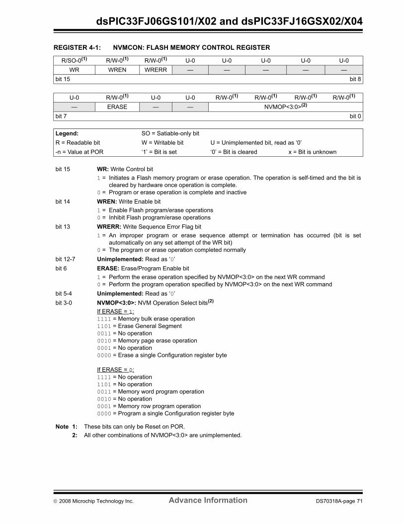
dsPIC33FJ06GS101/X02 and dsPIC33FJ16GSX02/X04
REGISTER 4-1: NVMCON: FLASH MEMORY CONTROL REGISTER
R/SO-0(1) R/W-0(1) R/W-0(1) U-0 U-0 U-0 U-0 U-0WR WREN WRERR — — — — —
bit 15 bit 8
U-0 R/W-0(1) U-0 U-0 R/W-0(1) R/W-0(1) R/W-0(1) R/W-0(1)
— ERASE — — NVMOP<3:0>(2)
bit 7 bit 0
Legend: SO = Satiable-only bitR = Readable bit W = Writable bit U = Unimplemented bit, read as ‘0’-n = Value at POR ‘1’ = Bit is set ‘0’ = Bit is cleared x = Bit is unknown
bit 15 WR: Write Control bit1 = Initiates a Flash memory program or erase operation. The operation is self-timed and the bit is
cleared by hardware once operation is complete. 0 = Program or erase operation is complete and inactive
bit 14 WREN: Write Enable bit1 = Enable Flash program/erase operations0 = Inhibit Flash program/erase operations
bit 13 WRERR: Write Sequence Error Flag bit1 = An improper program or erase sequence attempt or termination has occurred (bit is set
automatically on any set attempt of the WR bit)0 = The program or erase operation completed normally
bit 12-7 Unimplemented: Read as ‘0’bit 6 ERASE: Erase/Program Enable bit
1 = Perform the erase operation specified by NVMOP<3:0> on the next WR command0 = Perform the program operation specified by NVMOP<3:0> on the next WR command
bit 5-4 Unimplemented: Read as ‘0’bit 3-0 NVMOP<3:0>: NVM Operation Select bits(2)
If ERASE = 1:1111 = Memory bulk erase operation1101 = Erase General Segment0011 = No operation0010 = Memory page erase operation0001 = No operation0000 = Erase a single Configuration register byte
If ERASE = 0:1111 = No operation1101 = No operation0011 = Memory word program operation0010 = No operation0001 = Memory row program operation0000 = Program a single Configuration register byte
Note 1: These bits can only be Reset on POR.2: All other combinations of NVMOP<3:0> are unimplemented.
© 2008 Microchip Technology Inc. Advance Information DS70318A-page 71

dsPIC33FJ06GS101/X02 and dsPIC33FJ16GSX02/X04
REGISTER 4-2: NVMKEY: NONVOLATILE MEMORY KEY REGISTERU-0 U-0 U-0 U-0 U-0 U-0 U-0 U-0— — — — — — — —
bit 15 bit 8
W-0 W-0 W-0 W-0 W-0 W-0 W-0 W-0NVMKEY<7:0>
bit 7 bit 0
Legend: SO = Satiable-only bitR = Readable bit W = Writable bit U = Unimplemented bit, read as ‘0’-n = Value at POR ‘1’ = Bit is set ‘0’ = Bit is cleared x = Bit is unknown
bit 15-8 Unimplemented: Read as ‘0’bit 7-0 NVMKEY<7:0>: Key Register (write-only) bits
DS70318A-page 72 Advance Information © 2008 Microchip Technology Inc.

dsPIC33FJ06GS101/X02 and dsPIC33FJ16GSX02/X04
4.4.1 PROGRAMMING ALGORITHM FOR FLASH PROGRAM MEMORY
One row of program Flash memory can beprogrammed at a time. To achieve this, it is necessaryto erase the 8-row erase page that contains the desiredrow. The general process is:
1. Read eight rows of program memory(512 instructions) and store in data RAM.
2. Update the program data in RAM with thedesired new data.
3. Erase the block (see Example 4-1):a) Set the NVMOP bits (NVMCON<3:0>) to
‘0010’ to configure for block erase. Set theERASE (NVMCON<6>) and WREN(NVMCON<14>) bits.
b) Write the starting address of the page to beerased into the TBLPAG and W registers.
c) Write 0x55 to NVMKEY.d) Write 0xAA to NVMKEY.e) Set the WR bit (NVMCON<15>). The erase
cycle begins and the CPU stalls for theduration of the erase cycle. When the erase isdone, the WR bit is cleared automatically.
4. Write the first 64 instructions from data RAM intothe program memory buffers (see Example 4-2).
5. Write the program block to Flash memory:a) Set the NVMOP bits to ‘0001’ to configure
for row programming. Clear the ERASE bitand set the WREN bit.
b) Write 0x55 to NVMKEY.c) Write 0xAA to NVMKEY.d) Set the WR bit. The programming cycle
begins and the CPU stalls for the duration ofthe write cycle. When the write to Flashmemory is done, the WR bit is clearedautomatically.
6. Repeat steps 4 and 5, using the next available64 instructions from the block in data RAM byincrementing the value in TBLPAG, until all512 instructions are written back to Flash memory.
For protection against accidental operations, the writeinitiate sequence for NVMKEY must be used to allowany erase or program operation to proceed. After theprogramming command has been executed, the userapplication must wait for the programming time untilprogramming is complete. The two instructionsfollowing the start of the programming sequenceshould be NOPs, as shown in Example 4-3.
EXAMPLE 4-1: ERASING A PROGRAM MEMORY PAGE ; Set up NVMCON for block erase operation
MOV #0x4042, W0 ;MOV W0, NVMCON ; Initialize NVMCON
; Init pointer to row to be ERASEDMOV #tblpage(PROG_ADDR), W0 ; MOV W0, TBLPAG ; Initialize PM Page Boundary SFRMOV #tbloffset(PROG_ADDR), W0 ; Initialize in-page EA[15:0] pointerTBLWTL W0, [W0] ; Set base address of erase blockDISI #5 ; Block all interrupts with priority <7
; for next 5 instructionsMOV #0x55, W0 MOV W0, NVMKEY ; Write the 55 key MOV #0xAA, W1 ;MOV W1, NVMKEY ; Write the AA keyBSET NVMCON, #WR ; Start the erase sequence NOP ; Insert two NOPs after the eraseNOP ; command is asserted
© 2008 Microchip Technology Inc. Advance Information DS70318A-page 73

dsPIC33FJ06GS101/X02 and dsPIC33FJ16GSX02/X04
EXAMPLE 4-2: LOADING THE WRITE BUFFERS
EXAMPLE 4-3: INITIATING A PROGRAMMING SEQUENCE
; Set up NVMCON for row programming operationsMOV #0x4001, W0 ;MOV W0, NVMCON ; Initialize NVMCON
; Set up a pointer to the first program memory location to be written; program memory selected, and writes enabled
MOV #0x0000, W0 ; MOV W0, TBLPAG ; Initialize PM Page Boundary SFRMOV #0x6000, W0 ; An example program memory address
; Perform the TBLWT instructions to write the latches; 0th_program_word
MOV #LOW_WORD_0, W2 ; MOV #HIGH_BYTE_0, W3 ; TBLWTL W2, [W0] ; Write PM low word into program latchTBLWTH W3, [W0++] ; Write PM high byte into program latch
; 1st_program_wordMOV #LOW_WORD_1, W2 ; MOV #HIGH_BYTE_1, W3 ; TBLWTL W2, [W0] ; Write PM low word into program latchTBLWTH W3, [W0++] ; Write PM high byte into program latch
; 2nd_program_wordMOV #LOW_WORD_2, W2 ; MOV #HIGH_BYTE_2, W3 ; TBLWTL W2, [W0] ; Write PM low word into program latchTBLWTH W3, [W0++] ; Write PM high byte into program latch•••
; 63rd_program_wordMOV #LOW_WORD_31, W2 ; MOV #HIGH_BYTE_31, W3 ; TBLWTL W2, [W0] ; Write PM low word into program latchTBLWTH W3, [W0++] ; Write PM high byte into program latch
DISI #5 ; Block all interrupts with priority <7; for next 5 instructions
MOV #0x55, W0MOV W0, NVMKEY ; Write the 55 key MOV #0xAA, W1 ;MOV W1, NVMKEY ; Write the AA keyBSET NVMCON, #WR ; Start the erase sequence NOP ; Insert two NOPs after theNOP ; erase command is asserted
DS70318A-page 74 Advance Information © 2008 Microchip Technology Inc.
dsPIC33FJ06GS101/X02 and dsPIC33FJ16GSX02/X04
5.0 RESETS
The Reset module combines all reset sources andcontrols the device Master Reset Signal, SYSRST. Thefollowing is a list of device Reset sources:
• POR: Power-on Reset • BOR: Brown-out Reset• MCLR: Master Clear Pin Reset• SWR: RESET Instruction• WDTO: Watchdog Timer Reset• CM: Configuration Mismatch Reset• TRAPR: Trap Conflict Reset• IOPUWR: Illegal Condition Device Reset
- Illegal Opcode Reset- Uninitialized W Register Reset- Security Reset
A simplified block diagram of the Reset module isshown in Figure 5-1.
Any active source of reset will make the SYSRSTsignal active. On system Reset, some of the registersassociated with the CPU and peripherals are forced toa known Reset state and some are unaffected.
All types of device Reset sets a corresponding statusbit in the RCON register to indicate the type of Reset(see Register 5-1).
A POR clears all the bits, except for the POR bit(RCON<0>), that are set. The user application can setor clear any bit at any time during code execution. TheRCON bits only serve as status bits. Setting a particularReset status bit in software does not cause a deviceReset to occur.
The RCON register also has other bits associated withthe Watchdog Timer and device power-saving states.The function of these bits is discussed in other sectionsof this manual.
FIGURE 5-1: RESET SYSTEM BLOCK DIAGRAM
Note: This data sheet summarizes the featuresof the dsPIC33FJ06GS101/X02 anddsPIC33FJ16GSX02/X04 families ofdevices. It is not intended to be acomprehensive reference source. Tocomplement the information in this datasheet, refer to the dsPIC33F FamilyReference Manual, “Section 8. Reset”(DS70192), which is available from theMicrochip website (www.microchip.com).
Note: Refer to the specific peripheral section orSection 2.0 “CPU” of this manual forregister Reset states.
Note: The status bits in the RCON registershould be cleared after they are read sothat the next RCON register value after adevice Reset is meaningful.
MCLR
VDD
InternalRegulator
BOR
Sleep or Idle
RESET Instruction
WDTModule
Glitch Filter
Trap Conflict
Illegal Opcode
Uninitialized W Register
SYSRST
VDD RiseDetect
POR
Configuration Mismatch
© 2008 Microchip Technology Inc. Advance Information DS70318A-page 75

dsPIC33FJ06GS101/X02 and dsPIC33FJ16GSX02/X04
REGISTER 5-1: RCON: RESET CONTROL REGISTER(1)
R/W-0 R/W-0 U-0 U-0 U-0 U-0 R/W-0 R/W-0TRAPR IOPUWR — — — — CM VREGS
bit 15 bit 8
R/W-0 R/W-0 R/W-0 R/W-0 R/W-0 R/W-0 R/W-1 R/W-1EXTR SWR SWDTEN(2) WDTO SLEEP IDLE BOR POR
bit 7 bit 0
Legend:R = Readable bit W = Writable bit U = Unimplemented bit, read as ‘0’-n = Value at POR ‘1’ = Bit is set ‘0’ = Bit is cleared x = Bit is unknown
bit 15 TRAPR: Trap Reset Flag bit1 = A Trap Conflict Reset has occurred0 = A Trap Conflict Reset has not occurred
bit 14 IOPUWR: Illegal Opcode or Uninitialized W Access Reset Flag bit1 = An illegal opcode detection, an illegal address mode or uninitialized W register used as an Address
Pointer caused a Reset0 = An illegal opcode or uninitialized W Reset has not occurred
bit 13-10 Unimplemented: Read as ‘0’bit 9 CM: Configuration Mismatch Flag bit
1 = A configuration mismatch Reset has occurred0 = A configuration mismatch Reset has NOT occurred
bit 8 VREGS: Voltage Regulator Standby During Sleep bit1 = Voltage regulator is active during Sleep0 = Voltage regulator goes into Standby mode during Sleep
bit 7 EXTR: External Reset (MCLR) Pin bit1 = A Master Clear (pin) Reset has occurred0 = A Master Clear (pin) Reset has not occurred
bit 6 SWR: Software Reset (Instruction) Flag bit1 = A RESET instruction has been executed0 = A RESET instruction has not been executed
bit 5 SWDTEN: Software Enable/Disable of WDT bit(2)
1 = WDT is enabled0 = WDT is disabled
bit 4 WDTO: Watchdog Timer Time-out Flag bit1 = WDT time-out has occurred0 = WDT time-out has not occurred
bit 3 SLEEP: Wake-up from Sleep Flag bit1 = Device has been in Sleep mode0 = Device has not been in Sleep mode
bit 2 IDLE: Wake-up from Idle Flag bit1 = Device was in Idle mode0 = Device was not in Idle mode
Note 1: All of the Reset status bits can be set or cleared in software. Setting one of these bits in software does notcause a device Reset.
2: If the FWDTEN Configuration bit is ‘1’ (unprogrammed), the WDT is always enabled, regardless of theSWDTEN bit setting.
DS70318A-page 76 Advance Information © 2008 Microchip Technology Inc.

dsPIC33FJ06GS101/X02 and dsPIC33FJ16GSX02/X04
bit 1 BOR: Brown-out Reset Flag bit1 = A Brown-out Reset has occurred0 = A Brown-out Reset has not occurred
bit 0 POR: Power-on Reset Flag bit1 = A Power-up Reset has occurred0 = A Power-up Reset has not occurred
REGISTER 5-1: RCON: RESET CONTROL REGISTER(1) (CONTINUED)
Note 1: All of the Reset status bits can be set or cleared in software. Setting one of these bits in software does notcause a device Reset.
2: If the FWDTEN Configuration bit is ‘1’ (unprogrammed), the WDT is always enabled, regardless of theSWDTEN bit setting.
© 2008 Microchip Technology Inc. Advance Information DS70318A-page 77
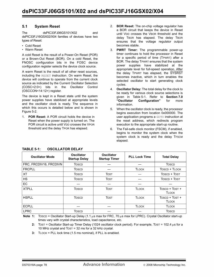
dsPIC33FJ06GS101/X02 and dsPIC33FJ16GSX02/X04
5.1 System ResetThe dsPIC33FJ06GS101/X02 anddsPIC33FJ16GSX02/X04 families of devices have twotypes of Reset:
• Cold Reset• Warm Reset
A cold Reset is the result of a Power-On Reset (POR)or a Brown-Out Reset (BOR). On a cold Reset, theFNOSC configuration bits in the FOSC deviceconfiguration register selects the device clock source.
A warm Reset is the result of all other reset sources,including the RESET instruction. On warm Reset, thedevice will continue to operate from the current clocksource as indicated by the Current Oscillator Selection(COSC<2:0>) bits in the Oscillator Control(OSCCON<14:12>) register.
The device is kept in a Reset state until the systempower supplies have stabilized at appropriate levelsand the oscillator clock is ready. The sequence inwhich this occurs is detailed below and is shown inFigure 5-2.
1. POR Reset: A POR circuit holds the device inReset when the power supply is turned on. ThePOR circuit is active until VDD crosses the VPORthreshold and the delay TPOR has elapsed.
2. BOR Reset: The on-chip voltage regulator hasa BOR circuit that keeps the device in Resetuntil VDD crosses the VBOR threshold and thedelay TBOR has elapsed. The delay TBORensures that the voltage regulator outputbecomes stable.
3. PWRT Timer: The programmable power-uptimer continues to hold the processor in Resetfor a specific period of time (TPWRT) after aBOR. The delay TPWRT ensures that the systempower supplies have stabilized at theappropriate level for full-speed operation. Afterthe delay TPWRT has elapsed, the SYSRSTbecomes inactive, which in turn enables theselected oscillator to start generating clockcycles.
4. Oscillator Delay: The total delay for the clock tobe ready for various clock source selections isgiven in Table 5-1. Refer to Section 7.0“Oscillator Configuration” for moreinformation.
5. When the oscillator clock is ready, the processorbegins execution from location 0x000000. Theuser application programs a GOTO instruction atthe reset address, which redirects programexecution to the appropriate start-up routine.
6. The Fail-safe clock monitor (FSCM), if enabled,begins to monitor the system clock when thesystem clock is ready and the delay TFSCMelapsed.
TABLE 5-1: OSCILLATOR DELAY
Oscillator Mode Oscillator Startup Delay
Oscillator Startup Timer PLL Lock Time Total Delay
FRC, FRCDIV16, FRCDIVN TOSCD — — TOSCD
FRCPLL TOSCD — TLOCK TOSCD + TLOCK
XT TOSCD TOST — TOSCD + TOST
HS TOSCD TOST — TOSCD + TOST
EC — — — —XTPLL TOSCD TOST TLOCK TOSCD + TOST +
TLOCK
HSPLL TOSCD TOST TLOCK TOSCD + TOST + TLOCK
ECPLL — — TLOCK TLOCK
LPRC TOSCD — — TOSCD
Note 1: TOSCD = Oscillator Start-up Delay (1.1 μs max for FRC, 70 μs max for LPRC). Crystal Oscillator start-up times vary with crystal characteristics, load capacitance, etc.
2: TOST = Oscillator Start-up Timer Delay (1024 oscillator clock period). For example, TOST = 102.4 μs for a 10 MHz crystal and TOST = 32 ms for a 32 kHz crystal.
3: TLOCK = PLL lock time (1.5 ms nominal), if PLL is enabled.
DS70318A-page 78 Advance Information © 2008 Microchip Technology Inc.

dsPIC33FJ06GS101/X02 and dsPIC33FJ16GSX02/X04
FIGURE 5-2: SYSTEM RESET TIMING
Reset RunDevice Status
VDD
VPOR
VborVBOR
POR Reset
BOR Reset
SYSRST
TPWRT
TPOR
TBOR
Oscillator Clock
TOSCD TOST TLOCK
Time
FSCMTFSCM
1
23
4
5
6
Note 1: POR Reset: A POR circuit holds the device in Reset when the power supply is turned on. The POR circuit isactive until VDD crosses the VPOR threshold and the delay TPOR has elapsed.
2: BOR Reset: The on-chip voltage regulator has a BOR circuit that keeps the device in Reset until VDD crossesthe VBOR threshold and the delay TBOR has elapsed. The delay TBOR ensures the voltage regulator outputbecomes stable.
3: PWRT Timer: The programmable power-up timer continues to hold the processor in Reset for a specific periodof time (TPWRT) after a BOR. The delay TPWRT ensures that the system power supplies have stabilized at theappropriate level for full-speed operation. After the delay TPWRT has elapsed, the SYSRST becomes inactive,which in turn enables the selected oscillator to start generating clock cycles.
4: Oscillator Delay: The total delay for the clock to be ready for various clock source selections are given inTable 5-1. Refer to Section 7.0 “Oscillator Configuration” for more information.
5: When the oscillator clock is ready, the processor begins execution from location 0x000000. The user applicationprograms a GOTO instruction at the reset address, which redirects program execution to the appropriate start-uproutine.
6: If Fail-Safe Clock Monitor (FSCM) is enabled, it begins to monitor the system clock when the system clock isready and the delay TFSCM elapsed.
© 2008 Microchip Technology Inc. Advance Information DS70318A-page 79

dsPIC33FJ06GS101/X02 and dsPIC33FJ16GSX02/X04
5.2 Power-on Reset (POR)A Power-on Reset (POR) circuit ensures the device isreset from power-on. The POR circuit is active untilVDD crosses the VPOR threshold and the delay TPORhas elapsed. The delay TPOR ensures the internaldevice bias circuits become stable.
The device supply voltage characteristics must meetthe specified starting voltage and rise raterequirements to generate the POR. Refer toSection 23.0 “Electrical Characteristics” for details.
The POR status (POR) bit in the Reset Control(RCON<0>) register is set to indicate the Power-onReset.
5.2.1 Brown-out Reset (BOR) and Power-up timer (PWRT)
The on-chip regulator has a Brown-out Reset (BOR)circuit that resets the device when the VDD is too low(VDD < VBOR) for proper device operation. The BORcircuit keeps the device in Reset until VDD crossesVBOR threshold and the delay TBOR has elapsed. Thedelay TBOR ensures the voltage regulator outputbecomes stable.
The BOR status (BOR) bit in the Reset Control(RCON<1>) register is set to indicate the Brown-outReset.
The device will not run at full speed after a BOR as theVDD should rise to acceptable levels for full-speedoperation. The PWRT provides power-up time delay(TPWRT) to ensure that the system power supplies havestabilized at the appropriate levels for full-speedoperation before the SYSRST is released.
The power-up timer delay (TPWRT) is programmed bythe Power-on Reset Timer Value Select(FPWRT<2:0>) bits in the POR Configuration(FPOR<2:0>) register, which provides eight settings(from 0 ms to 128 ms). Refer to Section 20.0 “SpecialFeatures” for further details.
Figure 5-3 shows the typical brown-out scenarios. Thereset delay (TBOR + TPWRT) is initiated each time VDDrises above the VBOR trip point
TABLE 5-2: OSCILLATOR DELAYSymbol Parameter Value
VPOR POR threshold 1.8V nominalTPOR POR extension time 30 μs maximumVBOR BOR threshold 2.5V nominalTBOR BOR extension time 100 μs maximumTPWRT Programmable power-up time delay 0-128 ms nominalTFSCM Fail-safe Clock Monitor Delay 900 μs maximum
Note: When the device exits the Resetcondition (begins normal operation), thedevice operating parameters (voltage,frequency, temperature, etc.) must bewithin their operating ranges, otherwisethe device may not function correctly.The user application must ensure thatthe delay between the time power isfirst applied, and the time SYSRSTbecomes inactive, is long enough to getall operating parameters withinspecification.
DS70318A-page 80 Advance Information © 2008 Microchip Technology Inc.

dsPIC33FJ06GS101/X02 and dsPIC33FJ16GSX02/X04
FIGURE 5-3: BROWN-OUT SITUATIONS
5.3 External Reset (EXTR)The external Reset is generated by driving the MCLRpin low. The MCLR pin is a Schmitt trigger input with anadditional glitch filter. Reset pulses that are longer thanthe minimum pulse width will generate a Reset. Referto Section 23.0 “Electrical Characteristics” forminimum pulse width specifications. The ExternalReset (MCLR) Pin (EXTR) bit in the Reset Control(RCON) register is set to indicate the MCLR Reset.
5.3.0.1 EXTERNAL SUPERVISORY CIRCUIT
Many systems have external supervisory circuits thatgenerate reset signals to Reset multiple devices in thesystem. This external Reset signal can be directlyconnected to the MCLR pin to Reset the device whenthe rest of system is Reset.
5.3.0.2 INTERNAL SUPERVISORY CIRCUITWhen using the internal power supervisory circuit toReset the device, the external reset pin (MCLR) shouldbe tied directly or resistively to VDD. In this case, theMCLR pin will not be used to generate a Reset. Theexternal reset pin (MCLR) does not have an internalpull-up and must not be left unconnected.
5.4 Software RESET Instruction (SWR)Whenever the RESET instruction is executed, thedevice will assert SYSRST, placing the device in aspecial Reset state. This Reset state will notre-initialize the clock. The clock source in effect prior to
the RESET instruction will remain. SYSRST is releasedat the next instruction cycle, and the reset vector fetchwill commence.
The Software Reset (Instruction) Flag (SWR) bit in theReset Control (RCON<6>) register is set to indicatethe software Reset.
5.5 Watchdog Time-out Reset (WDTO)Whenever a Watchdog time-out occurs, the device willasynchronously assert SYSRST. The clock source willremain unchanged. A WDT time-out during Sleep orIdle mode will wake-up the processor, but will not resetthe processor.
The Watchdog Timer Time-out Flag (WDTO) bit in theReset Control (RCON<4>) register is set to indicatethe Watchdog Reset. Refer to Section 20.4“Watchdog Timer (WDT)” for more information onWatchdog Reset.
5.6 Trap Conflict Reset If a lower-priority hard trap occurs while ahigher-priority trap is being processed, a hard trapconflict Reset occurs. The hard traps includeexceptions of priority level 13 through level 15,inclusive. The address error (level 13) and oscillatorerror (level 14) traps fall into this category.
The Trap Reset Flag (TRAPR) bit in the Reset Control(RCON<15>) register is set to indicate the Trap ConflictReset. Refer to Section 6.0 “Interrupt Controller” formore information on trap conflict Resets.
VDD
SYSRST
VBOR
VDD
SYSRST
VBOR
VDD
SYSRST
VBOR TBOR + TPWRT
VDD dips before PWRT expires
TBOR + TPWRT
TBOR + TPWRT
© 2008 Microchip Technology Inc. Advance Information DS70318A-page 81
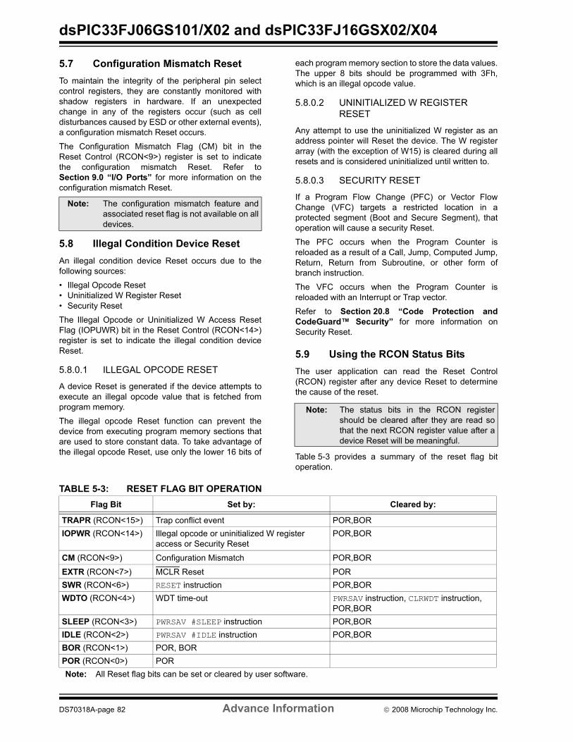
dsPIC33FJ06GS101/X02 and dsPIC33FJ16GSX02/X04
5.7 Configuration Mismatch Reset To maintain the integrity of the peripheral pin selectcontrol registers, they are constantly monitored withshadow registers in hardware. If an unexpectedchange in any of the registers occur (such as celldisturbances caused by ESD or other external events),a configuration mismatch Reset occurs.
The Configuration Mismatch Flag (CM) bit in theReset Control (RCON<9>) register is set to indicatethe configuration mismatch Reset. Refer toSection 9.0 “I/O Ports” for more information on theconfiguration mismatch Reset.
5.8 Illegal Condition Device ResetAn illegal condition device Reset occurs due to thefollowing sources:
• Illegal Opcode Reset• Uninitialized W Register Reset• Security Reset
The Illegal Opcode or Uninitialized W Access ResetFlag (IOPUWR) bit in the Reset Control (RCON<14>)register is set to indicate the illegal condition deviceReset.
5.8.0.1 ILLEGAL OPCODE RESET
A device Reset is generated if the device attempts toexecute an illegal opcode value that is fetched fromprogram memory.
The illegal opcode Reset function can prevent thedevice from executing program memory sections thatare used to store constant data. To take advantage ofthe illegal opcode Reset, use only the lower 16 bits of
each program memory section to store the data values.The upper 8 bits should be programmed with 3Fh,which is an illegal opcode value.
5.8.0.2 UNINITIALIZED W REGISTER RESET
Any attempt to use the uninitialized W register as anaddress pointer will Reset the device. The W registerarray (with the exception of W15) is cleared during allresets and is considered uninitialized until written to.
5.8.0.3 SECURITY RESET
If a Program Flow Change (PFC) or Vector FlowChange (VFC) targets a restricted location in aprotected segment (Boot and Secure Segment), thatoperation will cause a security Reset.
The PFC occurs when the Program Counter isreloaded as a result of a Call, Jump, Computed Jump,Return, Return from Subroutine, or other form ofbranch instruction.
The VFC occurs when the Program Counter isreloaded with an Interrupt or Trap vector.
Refer to Section 20.8 “Code Protection andCodeGuard™ Security” for more information onSecurity Reset.
5.9 Using the RCON Status BitsThe user application can read the Reset Control(RCON) register after any device Reset to determinethe cause of the reset.
Table 5-3 provides a summary of the reset flag bitoperation.
TABLE 5-3: RESET FLAG BIT OPERATION
Note: The configuration mismatch feature andassociated reset flag is not available on alldevices.
Note: The status bits in the RCON registershould be cleared after they are read sothat the next RCON register value after adevice Reset will be meaningful.
Flag Bit Set by: Cleared by:
TRAPR (RCON<15>) Trap conflict event POR,BORIOPWR (RCON<14>) Illegal opcode or uninitialized W register
access or Security ResetPOR,BOR
CM (RCON<9>) Configuration Mismatch POR,BOR
EXTR (RCON<7>) MCLR Reset PORSWR (RCON<6>) RESET instruction POR,BORWDTO (RCON<4>) WDT time-out PWRSAV instruction, CLRWDT instruction,
POR,BORSLEEP (RCON<3>) PWRSAV #SLEEP instruction POR,BORIDLE (RCON<2>) PWRSAV #IDLE instruction POR,BORBOR (RCON<1>) POR, BORPOR (RCON<0>) PORNote: All Reset flag bits can be set or cleared by user software.
DS70318A-page 82 Advance Information © 2008 Microchip Technology Inc.
dsPIC33FJ06GS101/X02 and dsPIC33FJ16GSX02/X04
6.0 INTERRUPT CONTROLLER
The dsPIC33FJ06GS101/X02 anddsPIC33FJ16GSX02/X04 interrupt controller reduces thenumerous peripheral interrupt request signals to a singleinterrupt request signal to the dsPIC33FJ06GS101/X02and dsPIC33FJ16GSX02/X04 CPU. It has the followingfeatures:
• Up to eight processor exceptions and software traps
• Seven user-selectable priority levels• Interrupt Vector Table (IVT) with up to 118 vectors• A unique vector for each interrupt or exception
source• Fixed priority within a specified user priority level• Alternate Interrupt Vector Table (AIVT) for debug
support• Fixed interrupt entry and return latencies
6.1 Interrupt Vector TableThe Interrupt Vector Table (IVT) is shown in Figure 6-1.The IVT resides in program memory, starting atlocation 000004h. The IVT contains 126 vectorsconsisting of eight nonmaskable trap vectors plus upto 118 sources of interrupt. In general, each interruptsource has its own vector. Each interrupt vectorcontains a 24-bit-wide address. The value programmedinto each interrupt vector location is the startingaddress of the associated Interrupt Service Routine(ISR).
Interrupt vectors are prioritized in terms of their naturalpriority. This priority is linked to their position in thevector table. Lower addresses generally have a highernatural priority. For example, the interrupt associatedwith vector 0 will take priority over interrupts at anyother vector address.
The dsPIC33FJ06GS101/X02 anddsPIC33FJ16GSX02/X04 devices implement up to 35unique interrupts and 4 non-maskable traps. These aresummarized in Table 6-1.
6.1.1 ALTERNATE INTERRUPT VECTOR TABLE
The Alternate Interrupt Vector Table (AIVT) is locatedafter the IVT, as shown in Figure 6-1. Access to theAIVT is provided by the ALTIVT control bit(INTCON2<15>). If the ALTIVT bit is set, all interruptand exception processes use the alternate vectorsinstead of the default vectors. The alternate vectors areorganized in the same manner as the default vectors.
The AIVT supports debugging by providing a means toswitch between an application and a supportenvironment without requiring the interrupt vectors tobe reprogrammed. This feature also enables switchingbetween applications for evaluation of differentsoftware algorithms at run time. If the AIVT is notneeded, the AIVT should be programmed with thesame addresses used in the IVT.
6.2 Reset SequenceA device Reset is not a true exception because theinterrupt controller is not involved in the Reset process.The dsPIC33FJ06GS101/X02 anddsPIC33FJ16GSX02/X04 device clears its registers inresponse to a Reset, which forces the PC to zero. Thedigital signal controller then begins program execution ata location 0x000000. A GOTO instruction at the Resetaddress can redirect program execution to theappropriate start-up routine.
Note: This data sheet summarizes the featuresof the dsPIC33FJ06GS101/X02 anddsPIC33FJ16GSX02/X04 families ofdevices. It is not intended to be acomprehensive reference source. Tocomplement the information in this datasheet, refer to the dsPIC33F FamilyReference Manual, “Section 41.Interrupts (Part IV)” (DS70300), which isavailable on the Microchip website(www.microchip.com).
Note: Any unimplemented or unused vectorlocations in the IVT and AIVT should beprogrammed with the address of a defaultinterrupt handler routine that contains aRESET instruction.
© 2008 Microchip Technology Inc. Advance Information DS70318A-page 83

dsPIC33FJ06GS101/X02 and dsPIC33FJ16GSX02/X04
FIGURE 6-1: dsPIC33FJ06GS101/X02 and dsPIC33FJ16GSX02/X04 INTERRUPT VECTOR TABLE
Reset – GOTO Instruction 0x000000Reset – GOTO Address 0x000002
Reserved 0x000004Oscillator Fail Trap VectorAddress Error Trap Vector
Stack Error Trap VectorMath Error Trap Vector
ReservedReservedReserved
Interrupt Vector 0 0x000014Interrupt Vector 1
~~~
Interrupt Vector 52 0x00007CInterrupt Vector 53 0x00007EInterrupt Vector 54 0x000080
~~~
Interrupt Vector 116 0x0000FCInterrupt Vector 117 0x0000FE
Reserved 0x000100Reserved 0x000102Reserved
Oscillator Fail Trap VectorAddress Error Trap Vector
Stack Error Trap VectorMath Error Trap Vector
ReservedReservedReserved
Interrupt Vector 0 0x000114Interrupt Vector 1
~~~
Interrupt Vector 52 0x00017CInterrupt Vector 53 0x00017EInterrupt Vector 54 0x000180
~~~
Interrupt Vector 116Interrupt Vector 117 0x0001FE
Start of Code 0x000200
Dec
reas
ing
Nat
ural
Ord
er P
riorit
y
Interrupt Vector Table (IVT)(1)
Alternate Interrupt Vector Table (AIVT)(1)
Note 1: See Table 6-1 for the list of implemented interrupt vectors.
DS70318A-page 84 Advance Information © 2008 Microchip Technology Inc.

dsPIC33FJ06GS101/X02 and dsPIC33FJ16GSX02/X04
TABLE 6-1: INTERRUPT VECTORS
Vector Number
Interrupt Request
(IQR)IVT Address AIVT Address Interrupt Source
Highest Natural Order Priority8 0 0x000014 0x000114 INT0 – External Interrupt 09 1 0x000016 0x000116 IC1 – Input Capture 110 2 0x000018 0x000118 OC1 – Output Compare 111 3 0x00001A 0x00011A T1 – Timer112 4 0x00001C 0x00011C Reserved13 5 0x00001E 0x00011E IC2 – Input Capture 214 6 0x000020 0x000120 OC2 – Output Compare 215 7 0x000022 0x000122 T2 – Timer216 8 0x000024 0x000124 T3 – Timer317 9 0x000026 0x000126 SPI1E – SPI1 Fault18 10 0x000028 0x000128 SPI1 – SPI1 Transfer Done19 11 0x00002A 0x00012A U1RX – UART1 Receiver20 12 0x00002C 0x00012C U1TX – UART1 Transmitter21 13 0x00002E 0x00012E ADC – ADC Group Convert Done22 14 0x000030 0x000130 Reserved23 15 0x000032 0x000132 Reserved24 16 0x000034 0x000134 SI2C1 – I2C™1 Slave Event25 17 0x000036 0x000136 MI2C1 – I2C1 Master Event26 18 0x000038 0x000138 CMP1 – Analog Comparator 1 Interrupt27 19 0x00003A 0x00013A CN – Input Change Notification Interrupt28 20 0x00003C 0x00013C INT1 – External Interrupt 129 21 0x00003E 0x00013E Reserved30 22 0x000040 0x000140 Reserved31 23 0x000042 0x000142 Reserved32 24 0x000044 0x000144 Reserved33 25 0x000046 0x000146 Reserved34 26 0x000048 0x000148 Reserved35 27 0x00004A 0x00014A Reserved36 28 0x00004C 0x00014C Reserved37 29 0x00004E 0x00014E INT2 – External Interrupt 2
38-64 30-56 Reserved65 57 0x000086 0x000186 PWM PSEM Special Event Match
66-72 58-64 Reserved73 65 0x000096 0x000196 U1E – UART1 Error Interrupt
74-101 66-93 Reserved102 94 0x0000D0 0x0001D0 PWM 1 – PWM1 Interrupt103 95 0x0000D2 0x0001D2 PWM 2 – PWM2 Interrupt104 96 0x0000D4 0x0001D4 PWM 3 – PWM3 Interrupt105 97 0x0000D6 0x0001D6 PWM 4 – PWM4 Interrupt106 98 0x0000D8 0x0001D8 Reserved107 99 0x0000DA 0x0001DA Reserved108 100 0x0000DC 0x0001DC Reserved109 101 0x0000DE 0x0001DE Reserved110 102 0x0000E0 0x0001E0 Reserved111 103 0x0000E2 0x00001E2 CMP2 – Analog Comparator 2
© 2008 Microchip Technology Inc. Advance Information DS70318A-page 85

dsPIC33FJ06GS101/X02 and dsPIC33FJ16GSX02/X04
112 104 0x0000E4 0x0001E4 CMP3 – Analog Comparator 3113 105 0x0000E6 0x0001E6 CMP4 – Analog Comparator 4114 106 0x0000E8 0x0001E8 Reserved115 107 0x0000EA 0x0001EA Reserved116 108 0x0000EC 0x0001EC Reserved117 109 0x0000EE 0x0001EE Reserved118 110 0x0000F0 0x0001F0 ADC Pair 0 Convert Done119 111 0x0000F2 0x0001F2 ADC Pair 1 Convert Done120 112 0x0000F4 0x0001F4 ADC Pair 2 Convert Done121 113 0x0000F6 0x0001F6 ADC Pair 3 Convert Done122 114 0x0000F8 0x0001F8 ADC Pair 4 Convert Done123 115 0x0000FA 0x0001FA ADC Pair 5 Convert Done124 116 0x0000FC 0x0001FC ADC Pair 6 Convert Done125 117 0x0000FE 0x0001FE Reserved
Lowest Natural Order Priority
TABLE 6-1: INTERRUPT VECTORS (CONTINUED)
Vector Number
Interrupt Request
(IQR)IVT Address AIVT Address Interrupt Source
DS70318A-page 86 Advance Information © 2008 Microchip Technology Inc.

dsPIC33FJ06GS101/X02 and dsPIC33FJ16GSX02/X04
6.3 Interrupt Control and Status Registers
The dsPIC33FJ06GS101/X02 anddsPIC33FJ16GSX02/X04 devices implement 27registers for the interrupt controller:
• INTCON1 • INTCON2 • IFSx• IECx• IPCx • INTTREG
6.3.1 INTCON1 AND INTCON2Global interrupt control functions are controlled fromINTCON1 and INTCON2. INTCON1 contains theInterrupt Nesting Disable (NSTDIS) bit as well as thecontrol and status flags for the processor trap sources.The INTCON2 register controls the external interruptrequest signal behavior and the use of the AlternateInterrupt Vector Table.
6.3.2 IFS0-IFS7The IFS registers maintain all of the interrupt requestflags. Each source of interrupt has a status bit, which isset by the respective peripherals or external signal andis cleared via software.
6.3.3 IEC0-IEC7The IEC registers maintain all of the interrupt enablebits. These control bits are used to individually enableinterrupts from the peripherals or external signals.
6.3.4 IPC0-IPC29The IPC registers are used to set the interrupt prioritylevel for each source of interrupt. Each user interruptsource can be assigned to one of eight priority levels.
6.3.5 INTTREGThe INTTREG register contains the associatedinterrupt vector number and the new CPU interruptpriority level, which are latched into vector number(VECNUM<6:0>) and Interrupt level (ILR<3:0>) bitfields in the INTTREG register. The new interrupt prior-ity level is the priority of the pending interrupt.
The interrupt sources are assigned to the IFSx, IECxand IPCx registers in the same sequence that they arelisted in Table 6-1. For example, the INT0 (ExternalInterrupt 0) is shown as having vector number 8 and anatural order priority of 0. Thus, the INT0IF bit is foundin IFS0<0>, the INT0IE bit is found in IEC0<0>, and theINT0IP bits are found in the first position of IPC0(IPC0<2:0>).
6.3.6 STATUS/CONTROL REGISTERSAlthough they are not specifically part of the interruptcontrol hardware, two of the CPU Control registerscontain bits that control interrupt functionality.
• The CPU STATUS register, SR, contains theIPL<2:0> bits (SR<7:5>). These bits indicate thecurrent CPU interrupt priority level. The user canchange the current CPU priority level by writing tothe IPL bits.
• The CORCON register contains the IPL3 bitwhich, together with IPL<2:0>, indicates thecurrent CPU priority level. IPL3 is a read-only bitso that trap events cannot be masked by the usersoftware.
All Interrupt registers are described in Register 6-1through Register 6-35 in the following pages.
© 2008 Microchip Technology Inc. Advance Information DS70318A-page 87
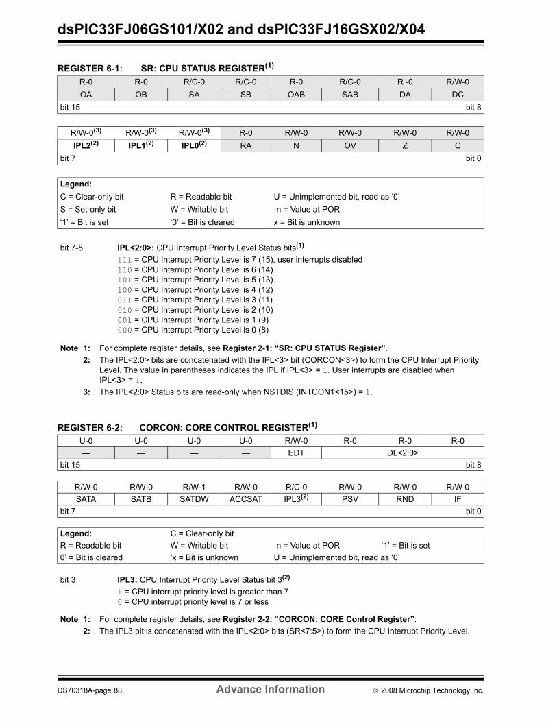
dsPIC33FJ06GS101/X02 and dsPIC33FJ16GSX02/X04
REGISTER 6-1: SR: CPU STATUS REGISTER(1)
REGISTER 6-2: CORCON: CORE CONTROL REGISTER(1)
R-0 R-0 R/C-0 R/C-0 R-0 R/C-0 R -0 R/W-0OA OB SA SB OAB SAB DA DC
bit 15 bit 8
R/W-0(3) R/W-0(3) R/W-0(3) R-0 R/W-0 R/W-0 R/W-0 R/W-0IPL2(2) IPL1(2) IPL0(2) RA N OV Z C
bit 7 bit 0
Legend:C = Clear-only bit R = Readable bit U = Unimplemented bit, read as ‘0’S = Set-only bit W = Writable bit -n = Value at POR‘1’ = Bit is set ‘0’ = Bit is cleared x = Bit is unknown
bit 7-5 IPL<2:0>: CPU Interrupt Priority Level Status bits(1)
111 = CPU Interrupt Priority Level is 7 (15), user interrupts disabled110 = CPU Interrupt Priority Level is 6 (14)101 = CPU Interrupt Priority Level is 5 (13)100 = CPU Interrupt Priority Level is 4 (12)011 = CPU Interrupt Priority Level is 3 (11)010 = CPU Interrupt Priority Level is 2 (10)001 = CPU Interrupt Priority Level is 1 (9)000 = CPU Interrupt Priority Level is 0 (8)
Note 1: For complete register details, see Register 2-1: “SR: CPU STATUS Register”.2: The IPL<2:0> bits are concatenated with the IPL<3> bit (CORCON<3>) to form the CPU Interrupt Priority
Level. The value in parentheses indicates the IPL if IPL<3> = 1. User interrupts are disabled when IPL<3> = 1.
3: The IPL<2:0> Status bits are read-only when NSTDIS (INTCON1<15>) = 1.
U-0 U-0 U-0 U-0 R/W-0 R-0 R-0 R-0— — — — EDT DL<2:0>
bit 15 bit 8
R/W-0 R/W-0 R/W-1 R/W-0 R/C-0 R/W-0 R/W-0 R/W-0SATA SATB SATDW ACCSAT IPL3(2) PSV RND IF
bit 7 bit 0
Legend: C = Clear-only bitR = Readable bit W = Writable bit -n = Value at POR ‘1’ = Bit is set0’ = Bit is cleared ‘x = Bit is unknown U = Unimplemented bit, read as ‘0’
bit 3 IPL3: CPU Interrupt Priority Level Status bit 3(2)
1 = CPU interrupt priority level is greater than 70 = CPU interrupt priority level is 7 or less
Note 1: For complete register details, see Register 2-2: “CORCON: CORE Control Register”.2: The IPL3 bit is concatenated with the IPL<2:0> bits (SR<7:5>) to form the CPU Interrupt Priority Level.
DS70318A-page 88 Advance Information © 2008 Microchip Technology Inc.

dsPIC33FJ06GS101/X02 and dsPIC33FJ16GSX02/X04
REGISTER 6-3: INTCON1: INTERRUPT CONTROL REGISTER 1
R/W-0 R/W-0 R/W-0 R/W-0 R/W-0 R/W-0 R/W-0 R/W-0NSTDIS OVAERR OVBERR COVAERR COVBERR OVATE OVBTE COVTE
bit 15 bit 8
R/W-0 R/W-0 U-0 R/W-0 R/W-0 R/W-0 R/W-0 U-0SFTACERR DIV0ERR — MATHERR ADDRERR STKERR OSCFAIL —
bit 7 bit 0
Legend:R = Readable bit W = Writable bit U = Unimplemented bit, read as ‘0’-n = Value at POR ‘1’ = Bit is set ‘0’ = Bit is cleared x = Bit is unknown
bit 15 NSTDIS: Interrupt Nesting Disable bit1 = Interrupt nesting is disabled0 = Interrupt nesting is enabled
bit 14 OVAERR: Accumulator A Overflow Trap Flag bit1 = Trap was caused by overflow of Accumulator A0 = Trap was not caused by overflow of Accumulator A
bit 13 OVBERR: Accumulator B Overflow Trap Flag bit1 = Trap was caused by overflow of Accumulator B0 = Trap was not caused by overflow of Accumulator B
bit 12 COVAERR: Accumulator A Catastrophic Overflow Trap Enable bit1 = Trap was caused by catastrophic overflow of Accumulator A 0 = Trap was not caused by catastrophic overflow of Accumulator A
bit 11 COVBERR: Accumulator B Catastrophic Overflow Trap Enable bit1 = Trap was caused by catastrophic overflow of Accumulator B 0 = Trap was not caused by catastrophic overflow of Accumulator B
bit 10 OVATE: Accumulator A Overflow Trap Enable bit1 = Trap overflow of Accumulator A0 = Trap disabled
bit 9 OVBTE: Accumulator B Overflow Trap Enable bit1 = Trap overflow of Accumulator B0 = Trap disabled
bit 8 COVTE: Catastrophic Overflow Trap Enable bit1 = Trap on catastrophic overflow of Accumulator A or B enabled0 = Trap disabled
bit 7 SFTACERR: Shift Accumulator Error Status bit1 = Math error trap was caused by an invalid accumulator shift0 = Math error trap was not caused by an invalid accumulator shift
bit 6 DIV0ERR: Arithmetic Error Status bit1 = Math error trap was caused by a divide by zero0 = Math error trap was not caused by a divide by zero
bit 5 Unimplemented: Read as ‘0’bit 4 MATHERR: Arithmetic Error Status bit
1 = Math error trap has occurred0 = Math error trap has not occurred
bit 3 ADDRERR: Address Error Trap Status bit1 = Address error trap has occurred0 = Address error trap has not occurred
© 2008 Microchip Technology Inc. Advance Information DS70318A-page 89

dsPIC33FJ06GS101/X02 and dsPIC33FJ16GSX02/X04
bit 2 STKERR: Stack Error Trap Status bit1 = Stack error trap has occurred0 = Stack error trap has not occurred
bit 1 OSCFAIL: Oscillator Failure Trap Status bit1 = Oscillator failure trap has occurred0 = Oscillator failure trap has not occurred
bit 0 Unimplemented: Read as ‘0’
REGISTER 6-3: INTCON1: INTERRUPT CONTROL REGISTER 1 (CONTINUED)
DS70318A-page 90 Advance Information © 2008 Microchip Technology Inc.

dsPIC33FJ06GS101/X02 and dsPIC33FJ16GSX02/X04
REGISTER 6-4: INTCON2: INTERRUPT CONTROL REGISTER 2R/W-0 R-0 U-0 U-0 U-0 U-0 U-0 U-0ALTIVT DISI — — — — — —
bit 15 bit 8
U-0 U-0 U-0 U-0 U-0 R/W-0 R/W-0 R/W-0— — — — — INT2EP INT1EP INT0EP
bit 7 bit 0
Legend:R = Readable bit W = Writable bit U = Unimplemented bit, read as ‘0’-n = Value at POR ‘1’ = Bit is set ‘0’ = Bit is cleared x = Bit is unknown
bit 15 ALTIVT: Enable Alternate Interrupt Vector Table bit1 = Use alternate vector table0 = Use standard (default) vector table
bit 14 DISI: DISI Instruction Status bit1 = DISI instruction is active0 = DISI instruction is not active
bit 13-3 Unimplemented: Read as ‘0’bit 2 INT2EP: External Interrupt 2 Edge Detect Polarity Select bit
1 = Interrupt on negative edge 0 = Interrupt on positive edge
bit 1 INT1EP: External Interrupt 1 Edge Detect Polarity Select bit1 = Interrupt on negative edge 0 = Interrupt on positive edge
bit 0 INT0EP: External Interrupt 0 Edge Detect Polarity Select bit1 = Interrupt on negative edge 0 = Interrupt on positive edge
© 2008 Microchip Technology Inc. Advance Information DS70318A-page 91
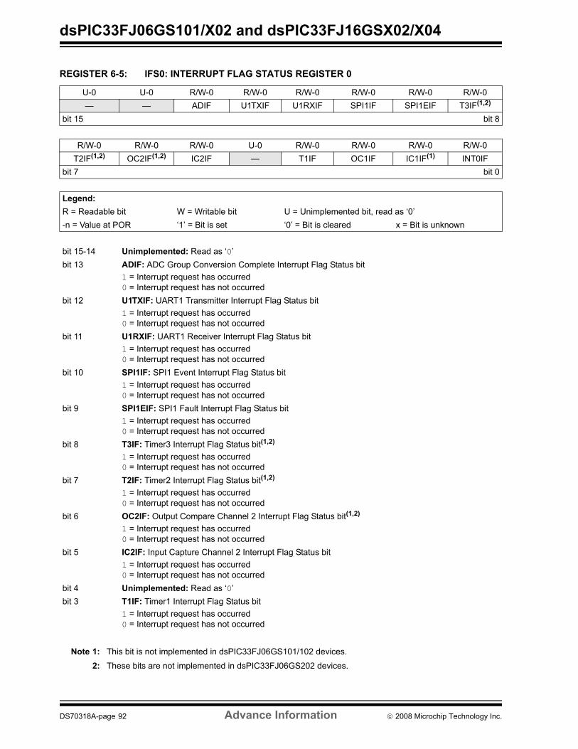
dsPIC33FJ06GS101/X02 and dsPIC33FJ16GSX02/X04
REGISTER 6-5: IFS0: INTERRUPT FLAG STATUS REGISTER 0
U-0 U-0 R/W-0 R/W-0 R/W-0 R/W-0 R/W-0 R/W-0— — ADIF U1TXIF U1RXIF SPI1IF SPI1EIF T3IF(1,2)
bit 15 bit 8
R/W-0 R/W-0 R/W-0 U-0 R/W-0 R/W-0 R/W-0 R/W-0T2IF(1,2) OC2IF(1,2) IC2IF — T1IF OC1IF IC1IF(1) INT0IF
bit 7 bit 0
Legend:R = Readable bit W = Writable bit U = Unimplemented bit, read as ‘0’-n = Value at POR ‘1’ = Bit is set ‘0’ = Bit is cleared x = Bit is unknown
bit 15-14 Unimplemented: Read as ‘0’bit 13 ADIF: ADC Group Conversion Complete Interrupt Flag Status bit
1 = Interrupt request has occurred0 = Interrupt request has not occurred
bit 12 U1TXIF: UART1 Transmitter Interrupt Flag Status bit1 = Interrupt request has occurred0 = Interrupt request has not occurred
bit 11 U1RXIF: UART1 Receiver Interrupt Flag Status bit1 = Interrupt request has occurred0 = Interrupt request has not occurred
bit 10 SPI1IF: SPI1 Event Interrupt Flag Status bit1 = Interrupt request has occurred0 = Interrupt request has not occurred
bit 9 SPI1EIF: SPI1 Fault Interrupt Flag Status bit1 = Interrupt request has occurred0 = Interrupt request has not occurred
bit 8 T3IF: Timer3 Interrupt Flag Status bit(1,2)
1 = Interrupt request has occurred0 = Interrupt request has not occurred
bit 7 T2IF: Timer2 Interrupt Flag Status bit(1,2)
1 = Interrupt request has occurred0 = Interrupt request has not occurred
bit 6 OC2IF: Output Compare Channel 2 Interrupt Flag Status bit(1,2)
1 = Interrupt request has occurred0 = Interrupt request has not occurred
bit 5 IC2IF: Input Capture Channel 2 Interrupt Flag Status bit1 = Interrupt request has occurred0 = Interrupt request has not occurred
bit 4 Unimplemented: Read as ‘0’bit 3 T1IF: Timer1 Interrupt Flag Status bit
1 = Interrupt request has occurred0 = Interrupt request has not occurred
Note 1: This bit is not implemented in dsPIC33FJ06GS101/102 devices.
2: These bits are not implemented in dsPIC33FJ06GS202 devices.
DS70318A-page 92 Advance Information © 2008 Microchip Technology Inc.

dsPIC33FJ06GS101/X02 and dsPIC33FJ16GSX02/X04
bit 2 OC1IF: Output Compare Channel 1 Interrupt Flag Status bit1 = Interrupt request has occurred0 = Interrupt request has not occurred
bit 1 IC1IF: Input Capture Channel 1 Interrupt Flag Status bit(1)
1 = Interrupt request has occurred0 = Interrupt request has not occurred
bit 0 INT0IF: External Interrupt 0 Flag Status bit1 = Interrupt request has occurred0 = Interrupt request has not occurred
REGISTER 6-5: IFS0: INTERRUPT FLAG STATUS REGISTER 0 (CONTINUED)
Note 1: This bit is not implemented in dsPIC33FJ06GS101/102 devices.
2: These bits are not implemented in dsPIC33FJ06GS202 devices.
© 2008 Microchip Technology Inc. Advance Information DS70318A-page 93

dsPIC33FJ06GS101/X02 and dsPIC33FJ16GSX02/X04
REGISTER 6-6: IFS1: INTERRUPT FLAG STATUS REGISTER 1U-0 U-0 R/W-0 U-0 U-0 U-0 U-0 U-0— — INT2IF — — — — —
bit 15 bit 8
U-0 U-0 U-0 R/W-0 R/W-0 R/W-0 R/W-0 R/W-0— — — INT1IF CNIF AC1IF(1) MI2C1IF SI2C1IF
bit 7 bit 0
Legend:R = Readable bit W = Writable bit U = Unimplemented bit, read as ‘0’-n = Value at POR ‘1’ = Bit is set ‘0’ = Bit is cleared x = Bit is unknown
bit 15-14 Unimplemented: Read as ‘0’bit 13 INT2IF: External Interrupt 2 Flag Status bit
1 = Interrupt request has occurred0 = Interrupt request has not occurred
bit 12-5 Unimplemented: Read as ‘0’bit 4 INT1IF: External Interrupt 1 Flag Status bit
1 = Interrupt request has occurred0 = Interrupt request has not occurred
bit 3 CNIF: Input Change Notification Interrupt Flag Status bit1 = Interrupt request has occurred0 = Interrupt request has not occurred
bit 2 AC1IF: Analog Comparator 1 Interrupt Flag Status bit(1)
1 = Interrupt request has occurred0 = Interrupt request has not occurred
bit 1 MI2C1IF: I2C1 Master Events Interrupt Flag Status bit1 = Interrupt request has occurred0 = Interrupt request has not occurred
bit 0 SI2C1IF: I2C1 Slave Events Interrupt Flag Status bit1 = Interrupt request has occurred0 = Interrupt request has not occurred
Note 1: This bit is not implemented in dsPIC33FJ16GS402/404 and dsPIC33FJ06GS101/102 devices.
DS70318A-page 94 Advance Information © 2008 Microchip Technology Inc.

dsPIC33FJ06GS101/X02 and dsPIC33FJ16GSX02/X04
REGISTER 6-7: IFS3: INTERRUPT FLAG STATUS REGISTER 3
REGISTER 6-8: IFS4: INTERRUPT FLAG STATUS REGISTER 4
U-0 U-0 U-0 U-0 U-0 U-0 R/W-0 U-0— — — — — — PSEMIF —
bit 15 bit 8
U-0 U-0 U-0 U-0 U-0 U-0 U-0 U-0— — — — — — — —
bit 7 bit 0
Legend:R = Readable bit W = Writable bit U = Unimplemented bit, read as ‘0’-n = Value at POR ‘1’ = Bit is set ‘0’ = Bit is cleared x = Bit is unknown
bit 15-10 Unimplemented: Read as ‘0’bit 9 PSEMIF: PWM Special Event Match Interrupt Flag Status bit
1 = Interrupt request has occurred0 = Interrupt request has not occurred
bit 8-0 Unimplemented: Read as ‘0’
U-0 U-0 U-0 U-0 U-0 U-0 U-0 U-0— — — — — — — —
bit 15 bit 8
U-0 U-0 U-0 U-0 U-0 U-0 R/W-0 U-0— — — — — — U1EIF —
bit 7 bit 0
Legend:R = Readable bit W = Writable bit U = Unimplemented bit, read as ‘0’-n = Value at POR ‘1’ = Bit is set ‘0’ = Bit is cleared x = Bit is unknown
bit 15-2 Unimplemented: Read as ‘0’bit 1 U1EIF: UART1 Error Interrupt Flag Status bit
1 = Interrupt request has occurred0 = Interrupt request has not occurred
bit 0 Unimplemented: Read as ‘0’
© 2008 Microchip Technology Inc. Advance Information DS70318A-page 95
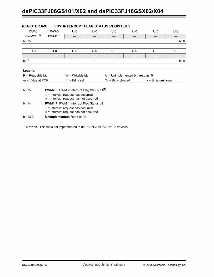
dsPIC33FJ06GS101/X02 and dsPIC33FJ16GSX02/X04
REGISTER 6-9: IFS5: INTERRUPT FLAG STATUS REGISTER 5R/W-0 R/W-0 U-0 U-0 U-0 U-0 U-0 U-0
PWM2IF(1) PWM1IF — — — — — —bit 15 bit 8
U-0 U-0 U-0 U-0 U-0 U-0 U-0 U-0— — — — — — — —
bit 7 bit 0
Legend:R = Readable bit W = Writable bit U = Unimplemented bit, read as ‘0’-n = Value at POR ‘1’ = Bit is set ‘0’ = Bit is cleared x = Bit is unknown
bit 15 PWM2IF: PWM 2 Interrupt Flag Status bit(1)
1 = Interrupt request has occurred0 = Interrupt request has not occurred
bit 14 PWM1IF: PWM 1 Interrupt Flag Status bit1 = Interrupt request has occurred0 = Interrupt request has not occurred
bit 13-0 Unimplemented: Read as ‘0’
Note 1: This bit is not implemented in dsPIC33FJ06GS101/102 devices.
DS70318A-page 96 Advance Information © 2008 Microchip Technology Inc.

dsPIC33FJ06GS101/X02 and dsPIC33FJ16GSX02/X04
REGISTER 6-10: IFS6: INTERRUPT FLAG STATUS REGISTER 6R/W-0 R/W-0 U-0 U-0 U-0 U-0 R/W-0 R/W-0
ADCP1IF ADCP0IF — — — — AC4IF(1,2) AC3IF(1,2)
bit 15 bit 8
R/W-0 U-0 U-0 U-0 U-0 U-0 R/W-0 R/W-0AC2IF(2) — — — — — PWM4IF(1,3) PWM3IF(4)
bit 7 bit 0
Legend:R = Readable bit W = Writable bit U = Unimplemented bit, read as ‘0’-n = Value at POR ‘1’ = Bit is set ‘0’ = Bit is cleared x = Bit is unknown
bit 15 ADCP1IF: ADC Pair 1 Conversion Done Interrupt Flag Status bit1 = Interrupt request has occurred0 = Interrupt request has not occurred
bit 14 ADCP0IF: ADC Pair 0 Conversion Done Interrupt Flag Status bit1 = Interrupt request has occurred0 = Interrupt request has not occurred
bit 13-10 Unimplemented: Read as ‘0bit 9 AC4IF: Analog Comparator 4 Interrupt Flag Status bit(1,2)
1 = Interrupt request has occurred0 = Interrupt request has not occurred
bit 8 AC3IF: Analog Comparator 3 Interrupt Flag Status bit(1,2)
1 = Interrupt request has occurred0 = Interrupt request has not occurred
bit 7 AC2IF: Analog Comparator 2 Interrupt Flag Status bit1 = Interrupt request has occurred0 = Interrupt request has not occurred
bit 6-2 Unimplemented: Read as ‘0’bit 1 PWM4IF: PWM 4 Interrupt Flag Status bit(3)
1 = Interrupt request has occurred0 = Interrupt request has not occurred
bit 0 PWM3IF: PWM 3 Interrupt Flag Status bit(4)
1 = Interrupt request has occurred0 = Interrupt request has not occurred
Note 1: These bits are unimplemented in dsPIC33FJ06GS202 devices.
2: These bits are unimplemented in dsPIC33FJ06GS101 and dsPIC33FJ16GS502 devices.
3: These bits are unimplemented in dsPIC33FJ16GS402/404/502 devices.
4: These bits are unimplemented in dsPIC33FJ06101/102/202 devices.
© 2008 Microchip Technology Inc. Advance Information DS70318A-page 97

dsPIC33FJ06GS101/X02 and dsPIC33FJ16GSX02/X04
REGISTER 6-11: IFS7: INTERRUPT FLAG STATUS REGISTER 7U-0 U-0 U-0 U-0 U-0 U-0 U-0 U-0— — — — — — — —
bit 15 bit 8
U-0 U-0 U-0 R/W-0 R/W-0 R/W-0 R/W-0 R/W-0— — — ADCP6IF ADCP5IF(1) ADCP4IF(1) ADCP3IF(2) ADCP2IF(3)
bit 7 bit 0
Legend:R = Readable bit W = Writable bit U = Unimplemented bit, read as ‘0’-n = Value at POR ‘1’ = Bit is set ‘0’ = Bit is cleared x = Bit is unknown
bit 15-5 Unimplemented: Read as ‘0’bit 4 ADCP6IF: ADC Pair 6 Conversion Done Interrupt Flag Status bit
1 = Interrupt request has occurred0 = Interrupt request has not occurred
bit 3 ADCP5IF: ADC Pair 5 Conversion Done Interrupt Flag Status bit(1)
1 = Interrupt request has occurred0 = Interrupt request has not occurred
bit 2 ADCP4IF: ADC Pair 4 Conversion Done Interrupt Flag Status bit(1)
1 = Interrupt request has occurred0 = Interrupt request has not occurred
bit 1 ADCP3IF: ADC Pair 3 Conversion Done Interrupt Flag Status bit(2)
1 = Interrupt request has occurred0 = Interrupt request has not occurred
bit 0 ADCP2IF: ADC Pair 2 Conversion Done Interrupt Flag Status bit(3)
1 = Interrupt request has occurred0 = Interrupt request has not occurred
Note 1: These bits are not implemented in dsPIC33FJ06GS101/102/202 and dsPIC33FJ16GS402/402/502devices.
2: This bit is not implemented in dsPIC33FJ06GS102/202 devices.
3: This bit is not implemented in dsPIC33FJ06GS101 devices.
DS70318A-page 98 Advance Information © 2008 Microchip Technology Inc.

dsPIC33FJ06GS101/X02 and dsPIC33FJ16GSX02/X04
REGISTER 6-12: IEC0: INTERRUPT ENABLE CONTROL REGISTER 0
U-0 U-0 R/W-0 R/W-0 R/W-0 R/W-0 R/W-0 R/W-0— — ADIE U1TXIE U1RXIE SPI1IE SPI1EIE T3IE(1,2)
bit 15 bit 8
R/W-0 R/W-0 R/W-0 U-0 R/W-0 R/W-0 R/W-0 R/W-0T2IE OC2IE(1,2) IC2IE(1,2) — T1IE OC1IE IC1IE(1) INT0IE
bit 7 bit 0
Legend:R = Readable bit W = Writable bit U = Unimplemented bit, read as ‘0’-n = Value at POR ‘1’ = Bit is set ‘0’ = Bit is cleared x = Bit is unknown
bit 15-14 Unimplemented: Read as ‘0’bit 13 ADIE: ADC1 Conversion Complete Interrupt Enable bit
1 = Interrupt request enabled0 = Interrupt request not enabled
bit 12 U1TXIE: UART1 Transmitter Interrupt Enable bit1 = Interrupt request enabled0 = Interrupt request not enabled
bit 11 U1RXIE: UART1 Receiver Interrupt Enable bit1 = Interrupt request enabled0 = Interrupt request not enabled
bit 10 SPI1IE: SPI1 Event Interrupt Enable bit1 = Interrupt request enabled0 = Interrupt request not enabled
bit 9 SPI1EIE: SPI1 Event Interrupt Enable bit1 = Interrupt request enabled0 = Interrupt request not enabled
bit 8 T3IE: Timer3 Interrupt Enable bit(1,2)
1 = Interrupt request enabled0 = Interrupt request not enabled
bit 7 T2IE: Timer2 Interrupt Enable bit1 = Interrupt request enabled0 = Interrupt request not enabled
bit 6 OC2IE: Output Compare Channel 2 Interrupt Enable bit(1,2)
1 = Interrupt request enabled0 = Interrupt request not enabled
bit 5 IC2IE: Input Capture Channel 2 Interrupt Enable bit(1,2)
1 = Interrupt request enabled0 = Interrupt request not enabled
bit 4 Unimplemented: Read as ‘0’bit 3 T1IE: Timer1 Interrupt Enable bit
1 = Interrupt request enabled0 = Interrupt request not enabled
Note 1: These bits are unimplemented in dsPIC33FJ06GS101/102 devices.
2: These bits are unimplemented in dsPIC33FJ06GS202 devices.
© 2008 Microchip Technology Inc. Advance Information DS70318A-page 99

dsPIC33FJ06GS101/X02 and dsPIC33FJ16GSX02/X04
bit 2 OC1IE: Output Compare Channel 1 Interrupt Enable bit1 = Interrupt request enabled0 = Interrupt request not enabled
bit 1 IC1IE: Input Capture Channel 1 Interrupt Enable bit(1)
1 = Interrupt request enabled0 = Interrupt request not enabled
bit 0 INT0IE: External Interrupt 0 Enable bit1 = Interrupt request enabled0 = Interrupt request not enabled
REGISTER 6-12: IEC0: INTERRUPT ENABLE CONTROL REGISTER 0 (CONTINUED)
Note 1: These bits are unimplemented in dsPIC33FJ06GS101/102 devices.
2: These bits are unimplemented in dsPIC33FJ06GS202 devices.
DS70318A-page 100 Advance Information © 2008 Microchip Technology Inc.
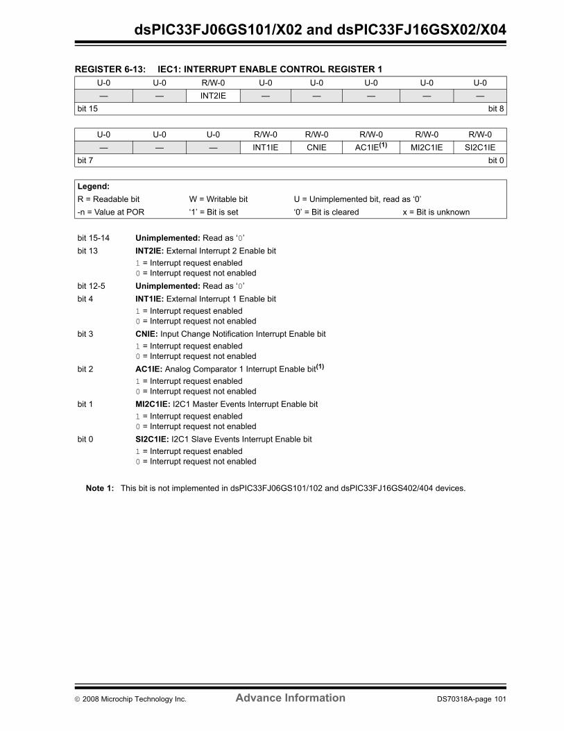
dsPIC33FJ06GS101/X02 and dsPIC33FJ16GSX02/X04
REGISTER 6-13: IEC1: INTERRUPT ENABLE CONTROL REGISTER 1U-0 U-0 R/W-0 U-0 U-0 U-0 U-0 U-0— — INT2IE — — — — —
bit 15 bit 8
U-0 U-0 U-0 R/W-0 R/W-0 R/W-0 R/W-0 R/W-0— — — INT1IE CNIE AC1IE(1) MI2C1IE SI2C1IE
bit 7 bit 0
Legend:R = Readable bit W = Writable bit U = Unimplemented bit, read as ‘0’-n = Value at POR ‘1’ = Bit is set ‘0’ = Bit is cleared x = Bit is unknown
bit 15-14 Unimplemented: Read as ‘0’bit 13 INT2IE: External Interrupt 2 Enable bit
1 = Interrupt request enabled0 = Interrupt request not enabled
bit 12-5 Unimplemented: Read as ‘0’bit 4 INT1IE: External Interrupt 1 Enable bit
1 = Interrupt request enabled0 = Interrupt request not enabled
bit 3 CNIE: Input Change Notification Interrupt Enable bit1 = Interrupt request enabled0 = Interrupt request not enabled
bit 2 AC1IE: Analog Comparator 1 Interrupt Enable bit(1)
1 = Interrupt request enabled0 = Interrupt request not enabled
bit 1 MI2C1IE: I2C1 Master Events Interrupt Enable bit1 = Interrupt request enabled0 = Interrupt request not enabled
bit 0 SI2C1IE: I2C1 Slave Events Interrupt Enable bit1 = Interrupt request enabled0 = Interrupt request not enabled
Note 1: This bit is not implemented in dsPIC33FJ06GS101/102 and dsPIC33FJ16GS402/404 devices.
© 2008 Microchip Technology Inc. Advance Information DS70318A-page 101

dsPIC33FJ06GS101/X02 and dsPIC33FJ16GSX02/X04
REGISTER 6-14: IEC3: INTERRUPT ENABLE CONTROL REGISTER 3
REGISTER 6-15: IEC4: INTERRUPT ENABLE CONTROL REGISTER 4
U-0 U-0 U-0 U-0 U-0 U-0 R/W-0 R/W-0— — — — — — PSEMIE —
bit 15 bit 8
U-0 U-0 U-0 U-0 U-0 U-0 R/W-0 U-0— — — — — — U1EIE —
bit 7 bit 0
Legend:R = Readable bit W = Writable bit U = Unimplemented bit, read as ‘0’-n = Value at POR ‘1’ = Bit is set ‘0’ = Bit is cleared x = Bit is unknown
bit 15-10 Unimplemented: Read as ‘0’bit 9 PSEMIE: PWM Special Event Match Interrupt Enable bit
1 = Interrupt request enabled0 = Interrupt request not enabled
bit 8-0 Unimplemented: Read as ‘0’
U-0 U-0 U-0 U-0 U-0 U-0 U-0 R/W-0— — — — — — — —
bit 15 bit 8
U-0 U-0 U-0 U-0 U-0 U-0 R/W-0 U-0— — — — — — U1EIE —
bit 7 bit 0
Legend:R = Readable bit W = Writable bit U = Unimplemented bit, read as ‘0’-n = Value at POR ‘1’ = Bit is set ‘0’ = Bit is cleared x = Bit is unknown
bit 15-2 Unimplemented: Read as ‘0’bit 1 U1EIE: UART1 Error Interrupt Enable bit
1 = Interrupt request enabled0 = Interrupt request not enabled
bit 0 Unimplemented: Read as ‘0’
DS70318A-page 102 Advance Information © 2008 Microchip Technology Inc.

dsPIC33FJ06GS101/X02 and dsPIC33FJ16GSX02/X04
REGISTER 6-16: IEC5: INTERRUPT ENABLE CONTROL REGISTER 5R/W-0 R/W-0 U-0 U-0 U-0 U-0 U-0 U-0
PWM2IE(1) PWM1IE — — — — — —bit 15 bit 8
U-0 U-0 U-0 U-0 U-0 U-0 U-0 U-0— — — — — — — —
bit 7 bit 0
Legend:R = Readable bit W = Writable bit U = Unimplemented bit, read as ‘0’-n = Value at POR ‘1’ = Bit is set ‘0’ = Bit is cleared x = Bit is unknown
bit 15 PWM2IE: PWM 2 Interrupt Enable bit(1)
1 = Interrupt request is enabled0 = Interrupt request is not enabled
bit 14 PWM1IE: PWM 1 Interrupt Enable bit1 = Interrupt request is enabled0 = Interrupt request is not enabled
bit 13-0 Unimplemented: Read as ‘0’
Note 1: This bit is unimplemented in dsPIC33FJ06GS101/102 devices.
© 2008 Microchip Technology Inc. Advance Information DS70318A-page 103

dsPIC33FJ06GS101/X02 and dsPIC33FJ16GSX02/X04
REGISTER 6-17: IEC6: INTERRUPT ENABLE CONTROL REGISTER 6R/W-0 R/W-0 U-0 U-0 U-0 U-0 R/W-0 R/W-0
ADCP1IE ADCP0IE — — — — AC4IE(1,2) AC3IE(1,2)
bit 15 bit 8
R/W-0 U-0 U-0 U-0 U-0 U-0 R/W-0 R/W-0AC2IE(2) — — — — — PWM4IE(1,3) PWM3IE(4)
bit 7 bit 0
Legend:R = Readable bit W = Writable bit U = Unimplemented bit, read as ‘0’-n = Value at POR ‘1’ = Bit is set ‘0’ = Bit is cleared x = Bit is unknown
bit 15 ADCP1IE: ADC Pair 1 Conversion Done Interrupt Enable bit1 = Interrupt request is enabled0 = Interrupt request is not enabled
bit 14 ADCP0IE: ADC Pair 0 Conversion Done Interrupt Enable bit1 = Interrupt request is enabled0 = Interrupt request is not enabled
bit 13-10 Unimplemented: Read as ‘0bit 9 AC4IE: Analog Comparator 4 Interrupt Enable bit(1,2)
1 = Interrupt request is enabled0 = Interrupt request is not enabled
bit 8 AC3IE: Analog Comparator 3 Interrupt Enable bit(1,2)
1 = Interrupt request is enabled0 = Interrupt request is not enabled
bit 7 AC2IE: Analog Comparator 2 Interrupt Enable bit1 = Interrupt request is enabled0 = Interrupt request is not enabled
bit 6-2 Unimplemented: Read as ‘0’bit 1 PWM4IE: PWM 4 Interrupt Enable bit(3)
1 = Interrupt request is enabled0 = Interrupt request is not enabled
bit 0 PWM3IE: PWM 3 Interrupt Enable bit(4)
1 = Interrupt request is enabled0 = Interrupt request is not enabled
Note 1: These bits are unimplemented in dsPIC33FJ06GS202 devices.
2: These bits are unimplemented in dsPIC33FJ06GS101 and dsPIC33FJ16GS502 devices.
3: These bits are unimplemented in dsPIC33FJ16GS402/404/502 devices.
4: These bits are unimplemented in dsPIC33FJ06101/102/202 devices.
DS70318A-page 104 Advance Information © 2008 Microchip Technology Inc.

dsPIC33FJ06GS101/X02 and dsPIC33FJ16GSX02/X04
REGISTER 6-18: IEC7: INTERRUPT ENABLE CONTROL REGISTER 7U-0 U-0 U-0 U-0 U-0 U-0 U-0 U-0— — — — — — — —
bit 15 bit 8
U-0 U-0 U-0 R/W-0 R/W-0 R/W-0 R/W-0 R/W-0— — — ADCP6IE ADCP5IE(1) ADCP4IE(1) ADCP3IE(2) ADCP2IE(3)
bit 7 bit 0
Legend:R = Readable bit W = Writable bit U = Unimplemented bit, read as ‘0’-n = Value at POR ‘1’ = Bit is set ‘0’ = Bit is cleared x = Bit is unknown
bit 15-5 Unimplemented: Read as ‘0’bit 4 ADCP6IE: ADC Pair 6 Conversion Done Interrupt Enable bit
1 = Interrupt request is enabled0 = Interrupt request is not enabled
bit ADCP5IE: ADC Pair 5 Conversion Done Interrupt Enable bit(1)
1 = Interrupt request is enabled0 = Interrupt request is not enabled
bit ADCP4IE: ADC Pair 4 Conversion Done Interrupt Enable bit(1)
1 = Interrupt request is enabled0 = Interrupt request is not enabled
bit ADCP3IE: ADC Pair 3 Conversion Done Interrupt Enable bit(2)
1 = Interrupt request is enabled0 = Interrupt request is not enabled
bit ADCP2IE: ADC Pair 2 Conversion Done Interrupt Enable bit(3)
1 = Interrupt request is enabled0 = Interrupt request is not enabled
Note 1: These bits are not implemented in dsPIC33FJ06GS101/102/202 and dsPIC33FJ16GS402/402/502devices.
2: This bit is not implemented in dsPIC33FJ06GS102/202 devices.
3: This bit is not implemented in dsPIC33FJ06GS101 devices.
© 2008 Microchip Technology Inc. Advance Information DS70318A-page 105

dsPIC33FJ06GS101/X02 and dsPIC33FJ16GSX02/X04
REGISTER 6-19: IPC0: INTERRUPT PRIORITY CONTROL REGISTER 0U-0 R/W-1 R/W-0 R/W-0 U-0 R/W-1 R/W-0 R/W-0— T1IP<2:0> — OC1IP<2:0>
bit 15 bit 8
U-0 R/W-1 R/W-0 R/W-0 U-0 R/W-1 R/W-0 R/W-0— IC1IP<2:0>(1) — INT0IP<2:0>
bit 7 bit 0
Legend:R = Readable bit W = Writable bit U = Unimplemented bit, read as ‘0’-n = Value at POR ‘1’ = Bit is set ‘0’ = Bit is cleared x = Bit is unknown
bit 15 Unimplemented: Read as ‘0’bit 14-12 T1IP<2:0>: Timer1 Interrupt Priority bits
111 = Interrupt is priority 7 (highest priority interrupt)•••001 = Interrupt is priority 1000 = Interrupt source is disabled
bit 11 Unimplemented: Read as ‘0’bit 10-8 OC1IP<2:0>: Output Compare Channel 1 Interrupt Priority bits
111 = Interrupt is priority 7 (highest priority interrupt)•••001 = Interrupt is priority 1000 = Interrupt source is disabled
bit 7 Unimplemented: Read as ‘0’bit 6-4 IC1IP<2:0>: Input Capture Channel 1 Interrupt Priority bits(1)
111 = Interrupt is priority 7 (highest priority interrupt)•••001 = Interrupt is priority 1000 = Interrupt source is disabled
bit 3 Unimplemented: Read as ‘0’bit 2-0 INT0IP<2:0>: External Interrupt 0 Priority bits
111 = Interrupt is priority 7 (highest priority interrupt)•••001 = Interrupt is priority 1000 = Interrupt source is disabled
Note 1: These bits are unimplemented in dsPIC33FJ06GS101/102 devices.
DS70318A-page 106 Advance Information © 2008 Microchip Technology Inc.

dsPIC33FJ06GS101/X02 and dsPIC33FJ16GSX02/X04
REGISTER 6-20: IPC1: INTERRUPT PRIORITY CONTROL REGISTER 1U-0 R/W-1 R/W-0 R/W-0 U-0 R/W-1 R/W-0 R/W-0— T2IP<2:0> — OC2IP<2:0>(1)
bit 15 bit 8
U-0 R/W-1 R/W-0 R/W-0 U-0 U-0 U-0 U-0— IC2IP<2:0>(1,2) — — — —
bit 7 bit 0
Legend:R = Readable bit W = Writable bit U = Unimplemented bit, read as ‘0’-n = Value at POR ‘1’ = Bit is set ‘0’ = Bit is cleared x = Bit is unknown
bit 15 Unimplemented: Read as ‘0’bit 14-12 T2IP<2:0>: Timer2 Interrupt Priority bits
111 = Interrupt is priority 7 (highest priority interrupt)•••001 = Interrupt is priority 1000 = Interrupt source is disabled
bit 11 Unimplemented: Read as ‘0’bit 10-8 OC2IP<2:0>: Output Compare Channel 2 Interrupt Priority bits(1)
111 = Interrupt is priority 7 (highest priority interrupt)•••001 = Interrupt is priority 1000 = Interrupt source is disabled
bit 7 Unimplemented: Read as ‘0’bit 6-4 IC2IP<2:0>: Input Capture Channel 2 Interrupt Priority bits(1,2)
111 = Interrupt is priority 7 (highest priority interrupt)•••001 = Interrupt is priority 1000 = Interrupt source is disabled
bit 3-0 Unimplemented: Read as ‘0’
Note 1: These bits are not implemented in dsPIC33FJ06GS101/202 devices.
2: These bits are not implemented in dsPIC33FJ06GS102 devices.
© 2008 Microchip Technology Inc. Advance Information DS70318A-page 107

dsPIC33FJ06GS101/X02 and dsPIC33FJ16GSX02/X04
REGISTER 6-21: IPC2: INTERRUPT PRIORITY CONTROL REGISTER 2U-0 R/W-1 R/W-0 R/W-0 U-0 R/W-1 R/W-0 R/W-0— U1RXIP<2:0> — SPI1IP<2:0>
bit 15 bit 8
U-0 R/W-1 R/W-0 R/W-0 U-0 R/W-1 R/W-0 R/W-0— SPI1EIP<2:0> — T3IP<2:0>(1)
bit 7 bit 0
Legend:R = Readable bit W = Writable bit U = Unimplemented bit, read as ‘0’-n = Value at POR ‘1’ = Bit is set ‘0’ = Bit is cleared x = Bit is unknown
bit 15 Unimplemented: Read as ‘0’bit 14-12 U1RXIP<2:0>: UART1 Receiver Interrupt Priority bits
111 = Interrupt is priority 7 (highest priority interrupt)•••001 = Interrupt is priority 1000 = Interrupt source is disabled
bit 11 Unimplemented: Read as ‘0’bit 10-8 SPI1IP<2:0>: SPI1 Event Interrupt Priority bits
111 = Interrupt is priority 7 (highest priority interrupt)•••001 = Interrupt is priority 1000 = Interrupt source is disabled
bit 7 Unimplemented: Read as ‘0’bit 6-4 SPI1EIP<2:0>: SPI1 Error Interrupt Priority bits
111 = Interrupt is priority 7 (highest priority interrupt)•••001 = Interrupt is priority 1000 = Interrupt source is disabled
bit 3 Unimplemented: Read as ‘0’bit 2-0 T3IP<2:0>: Timer3 Interrupt Priority bits(1)
111 = Interrupt is priority 7 (highest priority interrupt)•••001 = Interrupt is priority 1000 = Interrupt source is disabled
Note 1: These bits are not implemented in dsPIC33FJ06GS101/102/202 devices.
DS70318A-page 108 Advance Information © 2008 Microchip Technology Inc.

dsPIC33FJ06GS101/X02 and dsPIC33FJ16GSX02/X04
REGISTER 6-22: IPC3: INTERRUPT PRIORITY CONTROL REGISTER 3U-0 U-0 U-0 U-0 U-0 R/W-1 R/W-0 R/W-0— — — — — — — —
bit 15 bit 8
U-0 R/W-1 R/W-0 R/W-0 U-0 R/W-1 R/W-0 R/W-0— ADIP<2:0> — U1TXIP<2:0>
bit 7 bit 0
Legend:R = Readable bit W = Writable bit U = Unimplemented bit, read as ‘0’-n = Value at POR ‘1’ = Bit is set ‘0’ = Bit is cleared x = Bit is unknown
bit 15-7 Unimplemented: Read as ‘0’bit 6-4 ADIP<2:0>: ADC1 Conversion Complete Interrupt Priority bits
111 = Interrupt is priority 7 (highest priority interrupt)•••001 = Interrupt is priority 1000 = Interrupt source is disabled
bit 3 Unimplemented: Read as ‘0’bit 2-0 U1TXIP<2:0>: UART1 Transmitter Interrupt Priority bits
111 = Interrupt is priority 7 (highest priority interrupt)•••001 = Interrupt is priority 1000 = Interrupt source is disabled
© 2008 Microchip Technology Inc. Advance Information DS70318A-page 109

dsPIC33FJ06GS101/X02 and dsPIC33FJ16GSX02/X04
REGISTER 6-23: IPC4: INTERRUPT PRIORITY CONTROL REGISTER 4U-0 R/W-1 R/W-0 R/W-0 U-0 R/W-1 R/W-0 R/W-0— CNIP<2:0> — AC1IP<2:0>(1)
bit 15 bit 8
U-0 R/W-1 R/W-0 R/W-0 U-0 R/W-1 R/W-0 R/W-0— MI2C1IP<2:0> — SI2C1IP<2:0>
bit 7 bit 0
Legend:R = Readable bit W = Writable bit U = Unimplemented bit, read as ‘0’-n = Value at POR ‘1’ = Bit is set ‘0’ = Bit is cleared x = Bit is unknown
bit 15 Unimplemented: Read as ‘0’bit 14-12 CNIP<2:0>: Change Notification Interrupt Priority bits
111 = Interrupt is priority 7 (highest priority interrupt)•••001 = Interrupt is priority 1000 = Interrupt source is disabled
bit 11 Unimplemented: Read as ‘0’bit 10-8 AC1IP<2:0>: Analog Comparator 1 Interrupt Priority bits(1)
111 = Interrupt is priority 7 (highest priority interrupt)•••001 = Interrupt is priority 1000 = Interrupt source is disabled
bit 7 Unimplemented: Read as ‘0’bit 6-4 MI2C1IP<2:0>: I2C1 Master Events Interrupt Priority bits
111 = Interrupt is priority 7 (highest priority interrupt)•••001 = Interrupt is priority 1000 = Interrupt source is disabled
bit 3 Unimplemented: Read as ‘0’bit 2-0 SI2C1IP<2:0>: I2C1 Slave Events Interrupt Priority bits
111 = Interrupt is priority 7 (highest priority interrupt)•••001 = Interrupt is priority 1000 = Interrupt source is disabled
Note 1: These bits are not implemented in dsPIC33FJ06GS101/102 and dsPIC33FJ16GS402/404 devices.
DS70318A-page 110 Advance Information © 2008 Microchip Technology Inc.

dsPIC33FJ06GS101/X02 and dsPIC33FJ16GSX02/X04
REGISTER 6-24: IPC5: INTERRUPT PRIORITY CONTROL REGISTER 5
REGISTER 6-25: IPC7: INTERRUPT PRIORITY CONTROL REGISTER 7
U-0 U-0 U-0 U-0 U-0 U-0 U-0 U-0— — — — — — — —
bit 15 bit 8
U-0 U-0 U-0 U-0 U-0 R/W-1 R/W-0 R/W-0— — — — — INT1IP<2:0>
bit 7 bit 0
Legend:R = Readable bit W = Writable bit U = Unimplemented bit, read as ‘0’-n = Value at POR ‘1’ = Bit is set ‘0’ = Bit is cleared x = Bit is unknown
bit 15-3 Unimplemented: Read as ‘0’bit 2-0 INT1IP<2:0>: External Interrupt 1 Priority bits
111 = Interrupt is priority 7 (highest priority interrupt)•••001 = Interrupt is priority 1000 = Interrupt source is disabled
U-0 U-1 U-0 U-0 U-0 U-1 U-0 U-0— — — — — — — —
bit 15 bit 8
U-0 R/W-1 R/W-0 R/W-0 U-0 U-0 U-0 U-0— INT2IP<2:0> — — — —
bit 7 bit 0
Legend:R = Readable bit W = Writable bit U = Unimplemented bit, read as ‘0’-n = Value at POR ‘1’ = Bit is set ‘0’ = Bit is cleared x = Bit is unknown
bit 15-7 Unimplemented: Read as ‘0’bit 6-4 INT2IP<2:0>: External Interrupt 2 Priority bits
111 = Interrupt is priority 7 (highest priority interrupt)•••001 = Interrupt is priority 1000 = Interrupt source is disabled
bit 3-0 Unimplemented: Read as ‘0’
© 2008 Microchip Technology Inc. Advance Information DS70318A-page 111

dsPIC33FJ06GS101/X02 and dsPIC33FJ16GSX02/X04
REGISTER 6-26: IPC14: INTERRUPT PRIORITY CONTROL REGISTER 16
REGISTER 6-27: IPC16: INTERRUPT PRIORITY CONTROL REGISTER 16
U-0 U-0 U-0 U-0 U-0 U-0 U-0 U-0— — — — — — — —
bit 15 bit 8
U-0 R/W-1 R/W-0 R/W-0 U-0 U-0 U-0 U-0— PSEMIP<2:0> — — — —
bit 7 bit 0
Legend:R = Readable bit W = Writable bit U = Unimplemented bit, read as ‘0’-n = Value at POR ‘1’ = Bit is set ‘0’ = Bit is cleared x = Bit is unknown
bit 15-7 Unimplemented: Read as ‘0’bit 6-4 PSEMIP<2:0>: PWM Special Event Match Interrupt Priority bits
111 = Interrupt is priority 7 (highest priority interrupt)•••001 = Interrupt is priority 1000 = Interrupt source is disabled
bit 3-0 Unimplemented: Read as ‘0’
U-0 U-0 U-0 U-0 U-0 U-0 U-0 U-0— — — — — — — —
bit 15 bit 8
U-0 R/W-1 R/W-0 R/W-0 U-0 U-0 U-0 U-0— U1EIP<2:0> — — — —
bit 7 bit 0
Legend:R = Readable bit W = Writable bit U = Unimplemented bit, read as ‘0’-n = Value at POR ‘1’ = Bit is set ‘0’ = Bit is cleared x = Bit is unknown
bit 15-7 Unimplemented: Read as ‘0’bit 6-4 U1EIP<2:0>: UART1 Error Interrupt Priority bits
111 = Interrupt is priority 7 (highest priority interrupt)•••001 = Interrupt is priority 1000 = Interrupt source is disabled
bit 3-0 Unimplemented: Read as ‘0’
DS70318A-page 112 Advance Information © 2008 Microchip Technology Inc.

dsPIC33FJ06GS101/X02 and dsPIC33FJ16GSX02/X04
REGISTER 6-28: IPC23: INTERRUPT PRIORITY CONTROL REGISTER 23U-0 R/W-1 R/W-0 R/W-0 U-0 R/W-1 R/W-0 R/W-0— PWM2IP(1) — PWM1IP<2:0>
bit 15 bit 8
U-0 U-0 U-0 U-0 U-0 U-0 U-0 U-0— — — — — — — —
bit 7 bit 0
Legend:R = Readable bit W = Writable bit U = Unimplemented bit, read as ‘0’-n = Value at POR ‘1’ = Bit is set ‘0’ = Bit is cleared x = Bit is unknown
bit 15 Unimplemented: Read as ‘0’bit 14-12 PWM2IP<2:0>: PWM 2 Interrupt Priority bits(1)
111 = Interrupt is priority 7 (highest priority)•••001 = Interrupt is priority 1000 = Interrupt source is disabled
bit 11 Unimplemented: Read as ‘0’bit 10-8 PWM1IP<2:0>: PWM 1 Interrupt Priority bits
111 = Interrupt is priority 7 (highest priority)•••001 = Interrupt is priority 1000 = Interrupt source is disabled
bit 7-0 Unimplemented: Read as ‘0’
Note 1: These bits are not implemented in dsPIC33FJ06GS101/102 devices.
© 2008 Microchip Technology Inc. Advance Information DS70318A-page 113

dsPIC33FJ06GS101/X02 and dsPIC33FJ16GSX02/X04
REGISTER 6-29: IPC24: INTERRUPT PRIORITY CONTROL REGISTER 24U-0 U-0 U-0 U-0 U-0 U-0 U-0 U-0— — — — — — — —
bit 15 bit 8
U-0 R/W-1 R/W-0 R/W-0 U-0 R/W-1 R/W-0 R/W-0— PWM4P(1) — PWM3IP<2:0>(2)
bit 7 bit 0
Legend:R = Readable bit W = Writable bit U = Unimplemented bit, read as ‘0’-n = Value at POR ‘1’ = Bit is set ‘0’ = Bit is cleared x = Bit is unknown
bit 15-7 Unimplemented: Read as ‘0’bit 6-4 PWM4IP<2:0>: PWM 4 Interrupt Priority bits(1)
111 = Interrupt is priority 7 (highest priority)•••001 = Interrupt is priority 1000 = Interrupt source is disabled
bit 3 Unimplemented: Read as ‘0’bit 2-0 PWM3IP<2:0>: PWM 3 Interrupt Priority bits(2)
111 = Interrupt is priority 7 (highest priority)•••001 = Interrupt is priority 1000 = Interrupt source is disabled
Note 1: These bits are not implemented in dsPIC33FJ06GS202 and dsPIC33FJ16GS402/404 devices.
2: These bits are not implemented in dsPIC33FJ06101/102/202 devices.
DS70318A-page 114 Advance Information © 2008 Microchip Technology Inc.
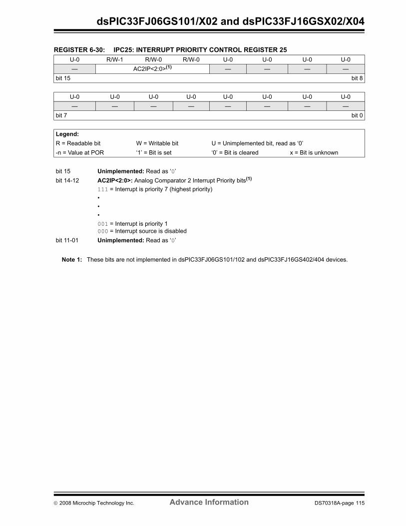
dsPIC33FJ06GS101/X02 and dsPIC33FJ16GSX02/X04
REGISTER 6-30: IPC25: INTERRUPT PRIORITY CONTROL REGISTER 25U-0 R/W-1 R/W-0 R/W-0 U-0 U-0 U-0 U-0— AC2IP<2:0>(1) — — — —
bit 15 bit 8
U-0 U-0 U-0 U-0 U-0 U-0 U-0 U-0— — — — — — — —
bit 7 bit 0
Legend:R = Readable bit W = Writable bit U = Unimplemented bit, read as ‘0’-n = Value at POR ‘1’ = Bit is set ‘0’ = Bit is cleared x = Bit is unknown
bit 15 Unimplemented: Read as ‘0’bit 14-12 AC2IP<2:0>: Analog Comparator 2 Interrupt Priority bits(1)
111 = Interrupt is priority 7 (highest priority)•••001 = Interrupt is priority 1000 = Interrupt source is disabled
bit 11-01 Unimplemented: Read as ‘0’
Note 1: These bits are not implemented in dsPIC33FJ06GS101/102 and dsPIC33FJ16GS402/404 devices.
© 2008 Microchip Technology Inc. Advance Information DS70318A-page 115

dsPIC33FJ06GS101/X02 and dsPIC33FJ16GSX02/X04
REGISTER 6-31: IPC26: INTERRUPT PRIORITY CONTROL REGISTER 26U-0 U-0 U-0 U-0 U-0 U-0 U-0 U-0— — — — — — — —
bit 15 bit 8
U-0 R/W-1 R/W-0 R/W-0 U-0 R/W-1 R/W-0 R/W-0— AC4IP<2:0>(1) — AC3IP<2:0>(1,2)
bit 7 bit 0
Legend:R = Readable bit W = Writable bit U = Unimplemented bit, read as ‘0’-n = Value at POR ‘1’ = Bit is set ‘0’ = Bit is cleared x = Bit is unknown
bit 15-7 Unimplemented: Read as ‘0’bit 6-4 AC4IP<2:0>: Analog Comparator 4 Interrupt Priority bits(1)
111 = Interrupt is priority 7 (highest priority)•••001 = Interrupt is priority 1000 = Interrupt source is disabled
bit 3 Unimplemented: Read as ‘0’bit 2-0 AC3IP<2:0>: Analog Comparator 3 Interrupt Priority bits(1,2)
111 = Interrupt is priority 7 (highest priority)•••001 = Interrupt is priority 1000 = Interrupt source is disabled
Note 1: These bits are not implemented in dsPIC33FJ06GS202 and dsPIC33FJ16GS402/404 devices.
2: These bits are not implemented in dsPIC33FJ06GS101/102 devices.
DS70318A-page 116 Advance Information © 2008 Microchip Technology Inc.

dsPIC33FJ06GS101/X02 and dsPIC33FJ16GSX02/X04
REGISTER 6-32: IPC27: INTERRUPT PRIORITY CONTROL REGISTER 27U-0 R/W-1 R/W-0 R/W-0 U-0 R/W-1 R/W-0 R/W-0— ADCP1IP<2:0> — ADCP0IP<2:0>(1)
bit 15 bit 8
U-0 U-0 U-0 U-0 U-0 U-0 U-0 U-0— — — — — — — —
bit 7 bit 0
Legend:R = Readable bit W = Writable bit U = Unimplemented bit, read as ‘0’-n = Value at POR ‘1’ = Bit is set ‘0’ = Bit is cleared x = Bit is unknown
bit 15 Unimplemented: Read as ‘0’bit 14-12 ADCP1IP<2:0>: ADC Pair 1 Conversion Done Interrupt Priority bits
111 = Interrupt is priority 7 (highest priority interrupt)•••001 = Interrupt is priority 1000 = Interrupt source is disabled
bit 11 Unimplemented: Read as ‘0’bit 10-8 ADCP0IP<2:0>: ADC Pair 0 Conversion Done Interrupt Priority bits(1)
111 = Interrupt is priority 7 (highest priority interrupt)•••001 = Interrupt is priority 1000 = Interrupt source is disabled
bit 7-0 Unimplemented: Read as ‘0’
© 2008 Microchip Technology Inc. Advance Information DS70318A-page 117

dsPIC33FJ06GS101/X02 and dsPIC33FJ16GSX02/X04
REGISTER 6-33: IPC28: INTERRUPT PRIORITY CONTROL REGISTER 28U-0 R/W-1 R/W-0 R/W-0 U-0 R/W-1 R/W-0 R/W-0— ADCP5IP<2:0>(4) — ADCP4IP<2:0>(4)
bit 15 bit 8
U-0 R/W-1 R/W-0 R/W-0 U-0 R/W-1 R/W-0 R/W-0— ADCP3IP<2:0>(2,3) — ADCP2IP<2:0>(1)
bit 7 bit 0
Legend:R = Readable bit W = Writable bit U = Unimplemented bit, read as ‘0’-n = Value at POR ‘1’ = Bit is set ‘0’ = Bit is cleared x = Bit is unknown
bit 15 Unimplemented: Read as ‘0’bit 14-12 ADCP5IP<2:0>: ADC Pair 5 Conversion Done Interrupt Priority bits(1,2,3,4)
111 = Interrupt is priority 7 (highest priority interrupt)•••001 = Interrupt is priority 1000 = Interrupt source is disabled
bit 11 Unimplemented: Read as ‘0’bit 10-8 ADCP4IP<2:0>: ADC Pair 4 Conversion Done Interrupt Priority bits
111 = Interrupt is priority 7 (highest priority interrupt)•••001 = Interrupt is priority 1000 = Interrupt source is disabled
bit 7 Unimplemented: Read as ‘0’bit 6-4 ADCP3IP<2:0>: ADC Pair 3 Conversion Done Interrupt Priority bits(2,3)
111 = Interrupt is priority 7 (highest priority interrupt)•••001 = Interrupt is priority 1000 = Interrupt source is disabled
bit 3 Unimplemented: Read as ‘0’bit 2-0 ADCP2IP<2:0>: ADC Pair 2 Conversion Done Interrupt Priority bits(1)
111 = Interrupt is priority 7 (highest priority interrupt)•••001 = Interrupt is priority 1000 = Interrupt source is disabled
Note 1: These bits are not implemented in dsPIC33FJ06GS101 devices.
2: These bits are not implemented in dsPIC33FJ06GS102 devices.
3: These bits are not implemented in dsPIC33FJ06GS202 devices.
4: These bits are implemented in dsPIC33FJ16GS504 devices only.
DS70318A-page 118 Advance Information © 2008 Microchip Technology Inc.
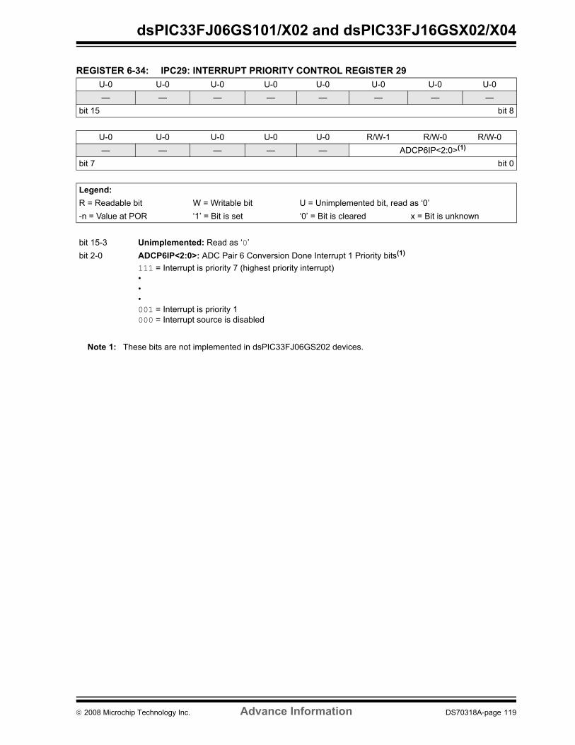
dsPIC33FJ06GS101/X02 and dsPIC33FJ16GSX02/X04
REGISTER 6-34: IPC29: INTERRUPT PRIORITY CONTROL REGISTER 29U-0 U-0 U-0 U-0 U-0 U-0 U-0 U-0— — — — — — — —
bit 15 bit 8
U-0 U-0 U-0 U-0 U-0 R/W-1 R/W-0 R/W-0— — — — — ADCP6IP<2:0>(1)
bit 7 bit 0
Legend:R = Readable bit W = Writable bit U = Unimplemented bit, read as ‘0’-n = Value at POR ‘1’ = Bit is set ‘0’ = Bit is cleared x = Bit is unknown
bit 15-3 Unimplemented: Read as ‘0’bit 2-0 ADCP6IP<2:0>: ADC Pair 6 Conversion Done Interrupt 1 Priority bits(1)
111 = Interrupt is priority 7 (highest priority interrupt)•••001 = Interrupt is priority 1000 = Interrupt source is disabled
Note 1: These bits are not implemented in dsPIC33FJ06GS202 devices.
© 2008 Microchip Technology Inc. Advance Information DS70318A-page 119

dsPIC33FJ06GS101/X02 and dsPIC33FJ16GSX02/X04
REGISTER 6-35: INTTREG: INTERRUPT CONTROL AND STATUS REGISTER
U-0 U-0 U-0 U-0 R-0 R-0 R-0 R-0— — — — ILR<3:0>
bit 15 bit 8
U-0 R-0 R-0 R-0 R-0 R-0 R-0 R-0— VECNUM<6:0>
bit 7 bit 0
Legend:R = Readable bit W = Writable bit U = Unimplemented bit, read as ‘0’-n = Value at POR ‘1’ = Bit is set ‘0’ = Bit is cleared x = Bit is unknown
bit 15-12 Unimplemented: Read as ‘0’bit 11-8 ILR: New CPU Interrupt Priority Level bits
1111 = CPU Interrupt Priority Level is 15 •••0001 = CPU Interrupt Priority Level is 10000 = CPU Interrupt Priority Level is 0
bit 7 Unimplemented: Read as ‘0’bit 6-0 VECNUM: Vector Number of Pending Interrupt bits
0111111 = Interrupt Vector pending is number 135 •••0000001 = Interrupt Vector pending is number 90000000 = Interrupt Vector pending is number 8
DS70318A-page 120 Advance Information © 2008 Microchip Technology Inc.

dsPIC33FJ06GS101/X02 and dsPIC33FJ16GSX02/X04
6.4 Interrupt Setup Procedures
6.4.1 INITIALIZATIONComplete the following steps to configure an interruptsource at initialization:
1. Set the NSTDIS bit (INTCON1<15>) if nestedinterrupts are not desired.
2. Select the user-assigned priority level for theinterrupt source by writing the control bits in theappropriate IPCx register. The priority level willdepend on the specific application and type ofinterrupt source. If multiple priority levels are notdesired, the IPCx register control bits for allenabled interrupt sources can be programmedto the same non-zero value.
3. Clear the interrupt flag status bit associated withthe peripheral in the associated IFSx register.
4. Enable the interrupt source by setting theinterrupt enable control bit associated with thesource in the appropriate IECx register.
6.4.2 INTERRUPT SERVICE ROUTINEThe method used to declare an ISR and initialize theIVT with the correct vector address depends on theprogramming language (C or assembler) and thelanguage development tool suite used to develop theapplication.
In general, the user application must clear the interruptflag in the appropriate IFSx register for the source ofinterrupt that the ISR handles. Otherwise, program willre-enter the ISR immediately after exiting the routine. Ifthe ISR is coded in assembly language, it must beterminated using a RETFIE instruction to unstack thesaved PC value, SRL value and old CPU priority level.
6.4.3 TRAP SERVICE ROUTINEA Trap Service Routine (TSR) is coded like an ISR,except that the appropriate trap status flag in theINTCON1 register must be cleared to avoid re-entryinto the TSR.
6.4.4 INTERRUPT DISABLEThe following steps outline the procedure to disable alluser interrupts:
1. Push the current SR value onto the softwarestack using the PUSH instruction.
2. Force the CPU to priority level 7 by inclusiveORing the value EOh with SRL.
To enable user interrupts, the POP instruction can beused to restore the previous SR value.
The DISI instruction provides a convenient way todisable interrupts of priority levels 1-6 for a fixed periodof time. Level 7 interrupt sources are not disabled bythe DISI instruction.
Note: At a device Reset, the IPCx registers areinitialized such that all user interruptsources are assigned to priority level 4.
Note: Only user interrupts with a priority level of7 or lower can be disabled. Trap sources(level 8-level 15) cannot be disabled.
© 2008 Microchip Technology Inc. Advance Information DS70318A-page 121

dsPIC33FJ06GS101/X02 and dsPIC33FJ16GSX02/X04
NOTES:
DS70318A-page 122 Advance Information © 2008 Microchip Technology Inc.

dsPIC33FJ06GS101/X02 and dsPIC33FJ16GSX02/X04
7.0 OSCILLATOR CONFIGURATION
The dsPIC33FJ06GS101/X02 and dsPIC33FJ16GSX02/X04 oscillator system provides:
• External and internal oscillator options as clock sources
• An on-chip Phase-Locked Loop (PLL) to scale the internal operating frequency to the required system clock frequency
• An internal FRC oscillator that can also be used with the PLL, thereby allowing full-speed operation without any external clock generation hardware
• Clock switching between various clock sources• Programmable clock postscaler for system power
savings• A Fail-Safe Clock Monitor (FSCM) that detects
clock failure and takes fail-safe measures• A Clock Control register (OSCCON)• Nonvolatile Configuration bits for main oscillator
selection.• Auxiliary PLL for ADC and PWM
A simplified diagram of the oscillator system is shownin Figure 7-1.
FIGURE 7-1: dsPIC33FJ06GS101/X02 and dsPIC33FJ16GSX02/X04 OSCILLATOR SYSTEM DIAGRAM
Note: This data sheet summarizes the featuresof the dsPIC33FJ06GS101/X02 anddsPIC33FJ16GSX02/X04 families ofdevices. It is not intended to be a compre-hensive reference source. To complementthe information in this data sheet, refer tothe dsPIC33F Family Reference Manual,“Section 42. Oscillator (Part IV)”(DS70307), which is available from theMicrochip website (www.microchip.com).
OSCI
OSCO
Primary Oscillator
XTPLL, HSPLL,
XT, HS, EC
FRCDIV<2:0>
WDT, PWRT, FSCM
FRCDIVN
FRCDIV16
ECPLL, FRCPLL
NOSC<2:0> FNOSC<2:0>
Reset
FRCOscillator
LPRCOscillator
DOZE<2:0>
S3
S1
S2
S1/S3
S7
S6
FRC
LPRC
S0
S5
÷ 16
Clock Switch
S7
Clock Fail
÷ 2
TUN<5:0>
PLL(1)
FCY
FOSC
FRC
DIV
DO
ZE
÷ N
ACLK
SELACLK APSTSCLR<2:0>
PWM/ADCPLLCLK
ENAPLL
POSCMD<1:0>
PLLCLK
APLLx16
ASRCSEL FRCSEL
POSCCLKFRCCLK
FRCCLK
POSCCLK
÷ N
ROSEL RODIV<3:0>
REFCLKOPOSCCLK
FCY
Reference Clock Generation
Auxiliary Clock Generation
RPx
Note 1: See Figure 7-2 for PLL details.
© 2008 Microchip Technology Inc. Advance Information DS70318A-page 123

dsPIC33FJ06GS101/X02 and dsPIC33FJ16GSX02/X04
7.1 CPU Clocking SystemThe dsPIC33FJ06GS101/X02 and dsPIC33FJ16GSX02/X04 devices provide six system clock options:
• Fast RC (FRC) Oscillator• FRC Oscillator with PLL• Primary (XT, HS or EC) Oscillator• Primary Oscillator with PLL• Low-Power RC (LPRC) Oscillator• FRC Oscillator with postscaler
7.1.1 SYSTEM CLOCK SOURCESThe Fast RC (FRC) internal oscillator runs at a nominalfrequency of 7.37 MHz. User software can tune theFRC frequency. User software can optionally specify afactor (ranging from 1:2 to 1:256) by which the FRCclock frequency is divided. This factor is selected usingthe FRCDIV<2:0> (CLKDIV<10:8>) bits.
The primary oscillator can use one of the following asits clock source:
• XT (Crystal): Crystals and ceramic resonators in the range of 3 MHz to 10 MHz. The crystal is connected to the OSC1 and OSC2 pins.
• HS (High-Speed Crystal): Crystals in the range of 10 MHz to 40 MHz. The crystal is connected to the OSC1 and OSC2 pins.
• EC (External Clock): External clock signal in the range of 0.8 MHz to 64 MHz. The external clock signal is directly applied to the OSC1 pin.
The LPRC internal oscIllator runs at a nominalfrequency of 32.768 kHz. It is also used as a referenceclock by the Watchdog Timer (WDT) and Fail-SafeClock Monitor (FSCM).
The clock signals generated by the FRC and primaryoscillators can be optionally applied to an on-chipPhase-Locked Loop (PLL) to provide a wide range ofoutput frequencies for device operation. PLLconfiguration is described in Section 7.1.3 “PLLConfiguration”.
7.1.2 SYSTEM CLOCK SELECTIONThe oscillator source used at a device Power-onReset event is selected using Configuration bit set-tings. The oscillator Configuration bit settings arelocated in the Configuration registers in the programmemory. (Refer to Section 20.1 “ConfigurationBits” for further details.) The Initial OscillatorSelection Configuration bits, FNOSC<2:0>(FOSCSEL<2:0>), and the Primary Oscillator ModeSelect Configuration bits, POSCMD<1:0>(FOSC<1:0>), select the oscillator source that is usedat a Power-on Reset. The FRC primary oscillator isthe default (unprogrammed) selection.
The Configuration bits allow users to choose among 12different clock modes, shown in Table 7-1.
The output of the oscillator (or the output of the PLL ifa PLL mode has been selected) FOSC is divided by 2 togenerate the device instruction clock (FCY). FCYdefines the operating speed of the device, and speedsup to 40 MHz are supported by thedsPIC33FJ06GS101/X02 and dsPIC33FJ16GSX02/X04 architecture.
Instruction execution speed or device operatingfrequency, FCY, is given by Equation 7-1.
EQUATION 7-1: DEVICE OPERATING FREQUENCY
TABLE 7-1: CONFIGURATION BIT VALUES FOR CLOCK SELECTION
FCY = FOSC/2
Oscillator Mode Oscillator Source POSCMD<1:0> FNOSC<2:0> Note
Fast RC Oscillator with Divide-by-N (FRCDIVN) Internal xx 111 1, 2Fast RC Oscillator with Divide-by-16 (FRCDIV16) Internal xx 110 1Low-Power RC Oscillator (LPRC) Internal xx 101 1Reserved Reserved xx 100 —Primary Oscillator (HS) with PLL (HSPLL) Primary 10 011 —Primary Oscillator (XT) with PLL (XTPLL) Primary 01 011 —Primary Oscillator (EC) with PLL (ECPLL) Primary 00 011 1Primary Oscillator (HS) Primary 10 010 —Primary Oscillator (XT) Primary 01 010 —Primary Oscillator (EC) Primary 00 010 1Fast RC Oscillator with PLL (FRCPLL) Internal xx 001 1Fast RC Oscillator (FRC) Internal xx 000 1Note 1: OSC2 pin function is determined by the OSCIOFNC Configuration bit.
2: This is the default oscillator mode for an unprogrammed (erased) device.
DS70318A-page 124 Advance Information © 2008 Microchip Technology Inc.
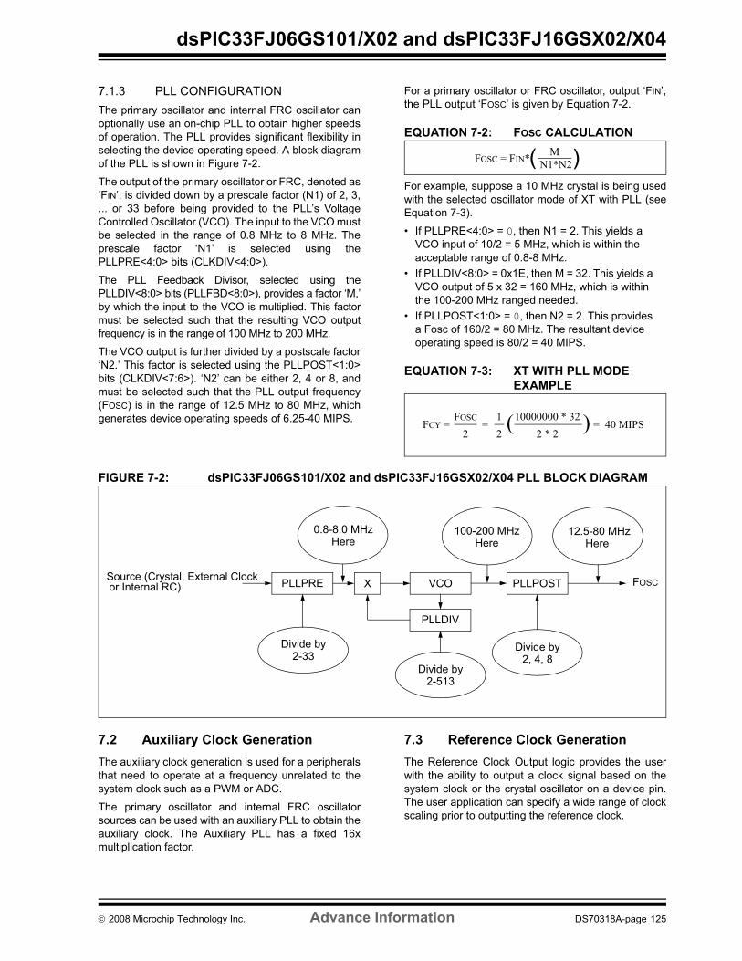
dsPIC33FJ06GS101/X02 and dsPIC33FJ16GSX02/X04
7.1.3 PLL CONFIGURATIONThe primary oscillator and internal FRC oscillator canoptionally use an on-chip PLL to obtain higher speedsof operation. The PLL provides significant flexibility inselecting the device operating speed. A block diagramof the PLL is shown in Figure 7-2.
The output of the primary oscillator or FRC, denoted as‘FIN’, is divided down by a prescale factor (N1) of 2, 3,... or 33 before being provided to the PLL’s VoltageControlled Oscillator (VCO). The input to the VCO mustbe selected in the range of 0.8 MHz to 8 MHz. Theprescale factor ‘N1’ is selected using thePLLPRE<4:0> bits (CLKDIV<4:0>).
The PLL Feedback Divisor, selected using thePLLDIV<8:0> bits (PLLFBD<8:0>), provides a factor ‘M,’by which the input to the VCO is multiplied. This factormust be selected such that the resulting VCO outputfrequency is in the range of 100 MHz to 200 MHz.
The VCO output is further divided by a postscale factor‘N2.’ This factor is selected using the PLLPOST<1:0>bits (CLKDIV<7:6>). ‘N2’ can be either 2, 4 or 8, andmust be selected such that the PLL output frequency(FOSC) is in the range of 12.5 MHz to 80 MHz, whichgenerates device operating speeds of 6.25-40 MIPS.
For a primary oscillator or FRC oscillator, output ‘FIN’,the PLL output ‘FOSC’ is given by Equation 7-2.
EQUATION 7-2: FOSC CALCULATION
For example, suppose a 10 MHz crystal is being usedwith the selected oscillator mode of XT with PLL (seeEquation 7-3).
• If PLLPRE<4:0> = 0, then N1 = 2. This yields a VCO input of 10/2 = 5 MHz, which is within the acceptable range of 0.8-8 MHz.
• If PLLDIV<8:0> = 0x1E, then M = 32. This yields a VCO output of 5 x 32 = 160 MHz, which is within the 100-200 MHz ranged needed.
• If PLLPOST<1:0> = 0, then N2 = 2. This provides a Fosc of 160/2 = 80 MHz. The resultant device operating speed is 80/2 = 40 MIPS.
EQUATION 7-3: XT WITH PLL MODE EXAMPLE
FIGURE 7-2: dsPIC33FJ06GS101/X02 and dsPIC33FJ16GSX02/X04 PLL BLOCK DIAGRAM
7.2 Auxiliary Clock GenerationThe auxiliary clock generation is used for a peripheralsthat need to operate at a frequency unrelated to thesystem clock such as a PWM or ADC.
The primary oscillator and internal FRC oscillatorsources can be used with an auxiliary PLL to obtain theauxiliary clock. The Auxiliary PLL has a fixed 16xmultiplication factor.
7.3 Reference Clock GenerationThe Reference Clock Output logic provides the userwith the ability to output a clock signal based on thesystem clock or the crystal oscillator on a device pin.The user application can specify a wide range of clockscaling prior to outputting the reference clock.
( ) M N1*N2FOSC = FIN*
FCY = FOSC
2= =
12(10000000 * 32
2 * 2) 40 MIPS
0.8-8.0 MHzHere
100-200 MHzHere
Divide by2, 4, 8
Divide by2-513
Divide by2-33
Source (Crystal, External Clock PLLPRE X VCO
PLLDIV
PLLPOSTor Internal RC)
12.5-80 MHzHere
FOSC
© 2008 Microchip Technology Inc. Advance Information DS70318A-page 125

dsPIC33FJ06GS101/X02 and dsPIC33FJ16GSX02/X04
REGISTER 7-1: OSCCON: OSCILLATOR CONTROL REGISTERU-0 R-0 R-0 R-0 U-0 R/W-y R/W-y R/W-y— COSC<2:0> — NOSC<2:0>
bit 15 bit 8
R/W-0 R/W-0 R-0 U-0 R/C-0 U-0 U-0 R/W-0CLKLOCK IOLOCK LOCK — CF — — OSWEN
bit 7 bit 0
Legend: y = Value set from Configuration bits on PORR = Readable bit W = Writable bit U = Unimplemented bit, read as ‘0’-n = Value at POR ‘1’ = Bit is set ‘0’ = Bit is cleared x = Bit is unknown
bit 15 Unimplemented: Read as ‘0’bit 14-12 COSC<2:0>: Current Oscillator Selection bits (read-only)
000 = Fast RC oscillator (FRC)001 = Fast RC oscillator (FRC) with PLL 010 = Primary oscillator (XT, HS, EC)011 = Primary oscillator (XT, HS, EC) with PLL 100 = Reserved101 = Low-Power RC oscillator (LPRC)110 = Fast RC oscillator (FRC) with Divide-by-16111 = Fast RC oscillator (FRC) with Divide-by-n
bit 11 Unimplemented: Read as ‘0’bit 10-8 NOSC<2:0>: New Oscillator Selection bits
000 = Fast RC oscillator (FRC)001 = Fast RC oscillator (FRC) with PLL 010 = Primary oscillator (XT, HS, EC)011 = Primary oscillator (XT, HS, EC) with PLL 100 = Reserved101 = Low-Power RC oscillator (LPRC)110 = Fast RC oscillator (FRC) with Divide-by-16111 = Fast RC oscillator (FRC) with Divide-by-n
bit 7 CLKLOCK: Clock Lock Enable bit If clock switching is enabled and FSCM is disabled, (FOSC<FCKSM> = 0b01)1 = Clock switching is disabled, system clock source is locked0 = Clock switching is enabled, system clock source can be modified by clock switching
bit 6 IOLOCK: Peripheral Pin Select Lock bit1 = Peripherial pin select is locked, write to peripheral pin select registers not allowed0 = Peripherial pin select is not locked, write to peripheral pin select registers allowed
bit 5 LOCK: PLL Lock Status bit (read-only) 1 = Indicates that PLL is in lock, or PLL start-up timer is satisfied0 = Indicates that PLL is out of lock, start-up timer is in progress or PLL is disabled
bit 4 Unimplemented: Read as ‘0’bit 3 CF: Clock Fail Detect bit (read/clear by application)
1 = FSCM has detected clock failure0 = FSCM has not detected clock failure
bit 2-1 Unimplemented: Read as ‘0’bit 0 OSWEN: Oscillator Switch Enable bit
1 = Request oscillator switch to selection specified by NOSC<2:0> bits0 = Oscillator switch is complete
DS70318A-page 126 Advance Information © 2008 Microchip Technology Inc.

dsPIC33FJ06GS101/X02 and dsPIC33FJ16GSX02/X04
REGISTER 7-2: CLKDIV: CLOCK DIVISOR REGISTERR/W-0 R/W-0 R/W-0 R/W-0 R/W-0 R/W-1 R/W-0 R/W-0ROI DOZE<2:0> DOZEN(1) FRCDIV<2:0>
bit 15 bit 8
R/W-0 R/W-1 U-0 R/W-0 R/W-0 R/W-0 R/W-0 R/W-0PLLPOST<1:0> — PLLPRE<4:0>
bit 7 bit 0
Legend: y = Value set from Configuration bits on PORR = Readable bit W = Writable bit U = Unimplemented bit, read as ‘0’-n = Value at POR ‘1’ = Bit is set ‘0’ = Bit is cleared x = Bit is unknown
bit 15 ROI: Recover on Interrupt bit1 = Interrupts will clear the DOZEN bit and the processor clock/peripheral clock ratio is set to 1:10 = Interrupts have no effect on the DOZEN bit
bit 14-12 DOZE<2:0>: Processor Clock Reduction Select bits000 = FCY/1001 = FCY/2010 = FCY/4011 = FCY/8 (default)100 = FCY/16101 = FCY/32110 = FCY/64111 = FCY/128
bit 11 DOZEN: DOZE Mode Enable bit(1)
1 = DOZE<2:0> field specifies the ratio between the peripheral clocks and the processor clocks0 = Processor clock/peripheral clock ratio forced to 1:1
bit 10-8 FRCDIV<2:0>: Internal Fast RC Oscillator Postscaler bits000 = FRC divide by 1 (default)001 = FRC divide by 2010 = FRC divide by 4011 = FRC divide by 8100 = FRC divide by 16101 = FRC divide by 32110 = FRC divide by 64111 = FRC divide by 256
bit 7-6 PLLPOST<1:0>: PLL VCO Output Divider Select bits (also denoted as ‘N2’, PLL postscaler)00 = Output/2 01 = Output/4 (default)10 = Reserved11 = Output/8
bit 5 Unimplemented: Read as ‘0’bit 4-0 PLLPRE<4:0>: PLL Phase Detector Input Divider bits (also denoted as ‘N1’, PLL prescaler)
00000 = Input/2 (default)00001 = Input/3••• 11111 = Input/33
Note 1: This bit is cleared when the ROI bit is set and an interrupt occurs.
© 2008 Microchip Technology Inc. Advance Information DS70318A-page 127

dsPIC33FJ06GS101/X02 and dsPIC33FJ16GSX02/X04
REGISTER 7-3: PLLFBD: PLL FEEDBACK DIVISOR REGISTERU-0 U-0 U-0 U-0 U-0 U-0 U-0 R/W-0— — — — — — — PLLDIV<8>
bit 15 bit 8
R/W-0 R/W-0 R/W-1 R/W-1 R/W-0 R/W-0 R/W-0 R/W-0PLLDIV<8:0>
bit 7 bit 0
Legend:R = Readable bit W = Writable bit U = Unimplemented bit, read as ‘0’-n = Value at POR ‘1’ = Bit is set ‘0’ = Bit is cleared x = Bit is unknown
bit 15-9 Unimplemented: Read as ‘0’bit 8-0 PLLDIV<8:0>: PLL Feedback Divisor bits (also denoted as ‘M’, PLL multiplier)
000000000 = 2000000001 = 3000000010 = 4•••000110000 = 50 (default)•••111111111 = 513
DS70318A-page 128 Advance Information © 2008 Microchip Technology Inc.

dsPIC33FJ06GS101/X02 and dsPIC33FJ16GSX02/X04
REGISTER 7-4: OSCTUN: FRC OSCILLATOR TUNING REGISTERU-0 U-0 U-0 U-0 U-0 U-0 U-0 U-0— — — — — — — —
bit 15 bit 8
U-0 U-0 R/W-0 R/W-0 R/W-0 R/W-0 R/W-0 R/W-0— — TUN<5:0>
bit 7 bit 0
Legend:R = Readable bit W = Writable bit U = Unimplemented bit, read as ‘0’-n = Value at POR ‘1’ = Bit is set ‘0’ = Bit is cleared x = Bit is unknown
bit 15-6 Unimplemented: Read as ‘0’bit 5-0 TUN<5:0>: FRC Oscillator Tuning bits
011111 = Center frequency + 11.625% (8.23 MHz)011110 = Center frequency + 11.25% (8.20 MHz)•••000001 = Center frequency + 0.375% (7.40 MHz) 000000 = Center frequency (7.37 MHz nominal)111111 = Center frequency -0.375% (7.345 MHz) •••100001 = Center frequency -11.625% (6.52 MHz) 100000 = Center frequency -12% (6.49 MHz)
© 2008 Microchip Technology Inc. Advance Information DS70318A-page 129
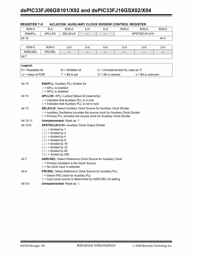
dsPIC33FJ06GS101/X02 and dsPIC33FJ16GSX02/X04
REGISTER 7-5: ACLKCON: AUXILIARY CLOCK DIVISOR CONTROL REGISTERR/W-0 R-0 R/W-0 U-0 U-0 R/W-0 R/W-0 R/W-0
ENAPLL APLLCK SELACLK — — APSTSCLR<2:0>bit 15 bit 0
R/W-0 R/W-0 U-0 U-0 U-0 U-0 U-0 U-0ASRCSEL FRCSEL — — — — — —
bit 7
Legend:R = Readable bit W = Writable bit U = Unimplemented bit, read as ‘0’-n = Value at POR ‘1’ = Bit is set ‘0’ = Bit is cleared x = Bit is unknown
bit 15 ENAPLL: Auxiliary PLL Enable bit1 = APLL is enabled0 = APLL is disabled
bit 14 APLLCK: APLL Locked Status bit (read-only)1 = Indicates that Auxiliary PLL is in lock0 = Indicates that Auxiliary PLL is not in lock
bit 13 SELACLK: Select Auxiliary Clock Source for Auxiliary Clock Divider1 = Auxiliary Oscillators provides the source clock for Auxiliary Clock Divider0 = Primary PLL provides the source clock for Auxiliary Clock Divider
bit 12-11 Unimplemented: Read as ‘0’bit 10-8 APSTSCLR<2:0>: Auxiliary Clock Output Divider
111 = divided by 1110 = divided by 2101 = divided by 4100 = divided by 8111 = divided by 16010 = divided by 32011 = divided by 64000 = divided by 256
bit 7 ASRCSEL: Select Reference Clock Source for Auxiliary Clock1 = Primary Oscillator is the Clock Source0 = No clock input is selected
bit 6 FRCSEL: Select Reference Clock Source for Auxiliary PLL1 = Select FRC clock for Auxiliary PLL0 = Input clock source is determined by ASRCSEL bit setting
bit 5-0 Unimplemented: Read as ‘0’
DS70318A-page 130 Advance Information © 2008 Microchip Technology Inc.
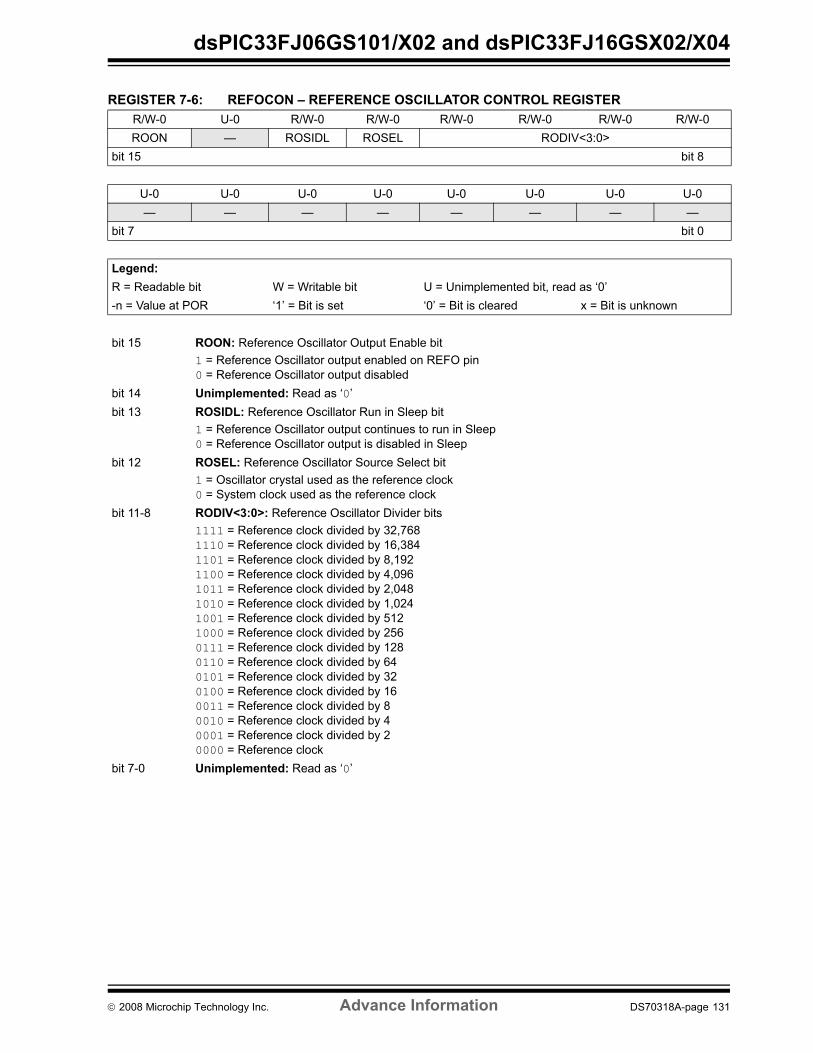
dsPIC33FJ06GS101/X02 and dsPIC33FJ16GSX02/X04
REGISTER 7-6: REFOCON – REFERENCE OSCILLATOR CONTROL REGISTERR/W-0 U-0 R/W-0 R/W-0 R/W-0 R/W-0 R/W-0 R/W-0ROON — ROSIDL ROSEL RODIV<3:0>
bit 15 bit 8
U-0 U-0 U-0 U-0 U-0 U-0 U-0 U-0— — — — — — — —
bit 7 bit 0
Legend:R = Readable bit W = Writable bit U = Unimplemented bit, read as ‘0’-n = Value at POR ‘1’ = Bit is set ‘0’ = Bit is cleared x = Bit is unknown
bit 15 ROON: Reference Oscillator Output Enable bit1 = Reference Oscillator output enabled on REFO pin0 = Reference Oscillator output disabled
bit 14 Unimplemented: Read as ‘0’bit 13 ROSIDL: Reference Oscillator Run in Sleep bit
1 = Reference Oscillator output continues to run in Sleep0 = Reference Oscillator output is disabled in Sleep
bit 12 ROSEL: Reference Oscillator Source Select bit1 = Oscillator crystal used as the reference clock0 = System clock used as the reference clock
bit 11-8 RODIV<3:0>: Reference Oscillator Divider bits1111 = Reference clock divided by 32,7681110 = Reference clock divided by 16,3841101 = Reference clock divided by 8,1921100 = Reference clock divided by 4,0961011 = Reference clock divided by 2,0481010 = Reference clock divided by 1,0241001 = Reference clock divided by 5121000 = Reference clock divided by 2560111 = Reference clock divided by 1280110 = Reference clock divided by 640101 = Reference clock divided by 320100 = Reference clock divided by 160011 = Reference clock divided by 80010 = Reference clock divided by 40001 = Reference clock divided by 20000 = Reference clock
bit 7-0 Unimplemented: Read as ‘0’
© 2008 Microchip Technology Inc. Advance Information DS70318A-page 131
dsPIC33FJ06GS101/X02 and dsPIC33FJ16GSX02/X04
7.4 Clock Switching OperationApplications are free to switch among any of the fourclock sources (Primary, LP, FRC and LPRC) undersoftware control at any time. To limit the possible sideeffects of this flexibility, dsPIC33FJ06GS101/X02 anddsPIC33FJ16GSX02/X04 devices have a safeguardlock built into the switch process.
7.4.1 ENABLING CLOCK SWITCHINGTo enable clock switching, the FCKSM1 Configurationbit in the Configuration register must be programmed to‘0’. (Refer to Section 20.1 “Configuration Bits” forfurther details.) If the FCKSM1 Configuration bit isunprogrammed (‘1’), the clock switching function andFail-Safe Clock Monitor function are disabled. This isthe default setting.
The NOSC control bits (OSCCON<10:8>) do notcontrol the clock selection when clock switching isdisabled. However, the COSC bits (OSCCON<14:12>)reflect the clock source selected by the FNOSCConfiguration bits.
The OSWEN control bit (OSCCON<0>) has no effectwhen clock switching is disabled. It is held at ‘0’ at alltimes.
7.4.2 OSCILLATOR SWITCHING SEQUENCE
To perform a clock switch, the following basic sequenceis required:
1. If desired, read the COSC bits(OSCCON<14:12>) to determine the currentoscillator source.
2. Perform the unlock sequence to allow a write tothe OSCCON register high byte.
3. Write the appropriate value to the NOSC controlbits (OSCCON<10:8>) for the new oscillatorsource.
4. Perform the unlock sequence to allow a write tothe OSCCON register low byte.
5. Set the OSWEN bit (OSCCON<0>) to initiatethe oscillator switch.
Once the basic sequence is completed, the systemclock hardware responds automatically as follows:
1. The clock switching hardware compares theCOSC status bits with the new value of theNOSC control bits. If they are the same, theclock switch is a redundant operation. In thiscase, the OSWEN bit is cleared automaticallyand the clock switch is aborted.
2. If a valid clock switch has been initiated, theLOCK (OSCCON<5>) and the CF(OSCCON<3>) status bits are cleared.
3. The new oscillator is turned on by the hardwareif it is not currently running. If a crystal oscillatormust be turned on, the hardware waits until theOscillator Start-up Timer (OST) expires. If thenew source is using the PLL, the hardware waitsuntil a PLL lock is detected (LOCK = 1).
4. The hardware waits for 10 clock cycles from thenew clock source and then performs the clockswitch.
5. The hardware clears the OSWEN bit to indicate asuccessful clock transition. In addition, the NOSCbit values are transferred to the COSC status bits.
6. The old clock source is turned off at this time,with the exception of LPRC (if WDT or FSCMare enabled) or LP (if LPOSCEN remains set).
7.5 Fail-Safe Clock Monitor (FSCM)The Fail-Safe Clock Monitor (FSCM) allows the deviceto continue to operate even in the event of an oscillatorfailure. The FSCM function is enabled by programming.If the FSCM function is enabled, the LPRC internaloscillator runs at all times (except during Sleep mode)and is not subject to control by the Watchdog Timer.
In the event of an oscillator failure, the FSCMgenerates a clock failure trap event and switches thesystem clock over to the FRC oscillator. Then theapplication program can either attempt to restart theoscillator or execute a controlled shutdown. The trapcan be treated as a warm Reset by simply loading theReset address into the oscillator fail trap vector.
If the PLL multiplier is used to scale the system clock,the internal FRC is also multiplied by the same factoron clock failure. Essentially, the device switches toFRC with PLL on a clock failure.
Note: Primary Oscillator mode has three differentsubmodes (XT, HS and EC), which aredetermined by the POSCMD<1:0>Configuration bits. While an applicationcan switch to and from Primary Oscillatormode in software, it cannot switch amongthe different primary submodes withoutreprogramming the device.
Note 1: The processor continues to execute codethroughout the clock switching sequence.Timing-sensitive code should not beexecuted during this time.
2: Direct clock switches between any primaryoscillator mode with PLL and FRCPLLmode are not permitted. This applies toclock switches in either direction. In theseinstances, the application must switch toFRC mode as a transition clock sourcebetween the two PLL modes.
DS70318A-page 132 Advance Information © 2008 Microchip Technology Inc.

dsPIC33FJ06GS101/X02 and dsPIC33FJ16GSX02/X04
8.0 POWER-SAVING FEATURES
The dsPIC33FJ06GS101/X02 and dsPIC33FJ16GSX02/X04 devices provide the ability to manage powerconsumption by selectively managing clocking to theCPU and the peripherals. In general, a lower clockfrequency and a reduction in the number of circuits beingclocked constitutes lower consumed power.dsPIC33FJ06GS101/X02 and dsPIC33FJ16GSX02/X04devices can manage power consumption in four differentways:
• Clock frequency• Instruction-based Sleep and Idle modes• Software-controlled Doze mode• Selective peripheral control in software
Combinations of these methods can be used toselectively tailor an application’s power consumptionwhile still maintaining critical application features, suchas timing-sensitive communications.
8.1 Clock Frequency and Clock Switching
The dsPIC33FJ06GS101/X02 anddsPIC33FJ16GSX02/X04 devices allow a wide rangeof clock frequencies to be selected under applicationcontrol. If the system clock configuration is not locked,users can choose low-power or high-precisionoscillators by simply changing the NOSC bits(OSCCON<10:8>). The process of changing a systemclock during operation, as well as limitations to theprocess, are discussed in more detail in Section 7.0“Oscillator Configuration”.
8.2 Instruction-Based Power-Saving Modes
The dsPIC33FJ06GS101/X02 anddsPIC33FJ16GSX02/X04 devices have two specialpower-saving modes that are entered through theexecution of a special PWRSAV instruction. Sleep modestops clock operation and halts all code execution. Idlemode halts the CPU and code execution, but allowsperipheral modules to continue operation. Theassembler syntax of the PWRSAV instruction is shown inExample 8-1.
Sleep and Idle modes can be exited as a result of anenabled interrupt, WDT time-out or a device Reset. Whenthe device exits these modes, it is said to wake-up.
8.2.1 SLEEP MODE The following occur in Sleep mode:
• The system clock source is shut down. If an on-chip oscillator is used, it is turned off.
• The device current consumption is reduced to a minimum, provided that no I/O pin is sourcing current.
• The Fail-Safe Clock Monitor does not operate, since the system clock source is disabled.
• The LPRC clock continues to run in Sleep mode if the WDT is enabled.
• The WDT, if enabled, is automatically cleared prior to entering Sleep mode.
• Some device features or peripherals may continue to operate. This includes the items such as the input change notification on the I/O ports or peripherals that use an external clock input.
• Any peripheral that requires the system clock source for its operation is disabled.
The device will wake-up from Sleep mode on any of thethese events:
• Any interrupt source that is individually enabled• Any form of device Reset• A WDT time-out
On wake-up from Sleep mode, the processor restartswith the same clock source that was active when Sleepmode was entered.
EXAMPLE 8-1: PWRSAV INSTRUCTION SYNTAX
Note: This data sheet summarizes the featuresof the dsPIC33FJ06GS101/X02 anddsPIC33FJ16GSX02/X04 families ofdevices. It is not intended to be acomprehensive reference source. Tocomplement the information in this datasheet, refer to the dsPIC33F FamilyReference Manual, “Section 9. Watch-dog Timer and Power Savings Modes”(DS70196), which is available from theMicrochip website (www.microchip.com). Note: SLEEP_MODE and IDLE_MODE are
constants defined in the assemblerinclude file for the selected device.
PWRSAV #SLEEP_MODE ; Put the device into SLEEP modePWRSAV #IDLE_MODE ; Put the device into IDLE mode
© 2008 Microchip Technology Inc. Advance Information DS70318A-page 133

dsPIC33FJ06GS101/X02 and dsPIC33FJ16GSX02/X04
8.2.2 IDLE MODE The following occur in Idle mode:
• The CPU stops executing instructions.• The WDT is automatically cleared.• The system clock source remains active. By
default, all peripheral modules continue to operate normally from the system clock source, but can also be selectively disabled (see Section 8.4 “Peripheral Module Disable”).
• If the WDT or FSCM is enabled, the LPRC also remains active.
The device will wake-up from Idle mode on any of theseevents:
• Any interrupt that is individually enabled• Any device Reset• A WDT time-out
On wake-up from Idle mode, the clock is reapplied tothe CPU and instruction execution begins immediately,starting with the instruction following the PWRSAVinstruction, or the first instruction in the ISR.
8.2.3 INTERRUPTS COINCIDENT WITH POWER SAVE INSTRUCTIONS
Any interrupt that coincides with the execution of aPWRSAV instruction is held off until entry into Sleep orIdle mode has completed. The device then wakes upfrom Sleep or Idle mode.
8.3 Doze ModeThe preferred strategies for reducing powerconsumption are changing clock speed and invokingone of the power-saving modes. In somecircumstances, this may not be practical. For example,it may be necessary for an application to maintainuninterrupted synchronous communication, even whileit is doing nothing else. Reducing system clock speedcan introduce communication errors, while using apower-saving mode can stop communicationscompletely.
Doze mode is a simple and effective alternative methodto reduce power consumption while the device is stillexecuting code. In this mode, the system clockcontinues to operate from the same source and at thesame speed. Peripheral modules continue to beclocked at the same speed, while the CPU clock speedis reduced. Synchronization between the two clockdomains is maintained, allowing the peripherals toaccess the SFRs while the CPU executes code at aslower rate.
Doze mode is enabled by setting the DOZEN bit(CLKDIV<11>). The ratio between peripheral and coreclock speed is determined by the DOZE<2:0> bits(CLKDIV<14:12>). There are eight possibleconfigurations, from 1:1 to 1:128, with 1:1 being thedefault setting.
Programs can use Doze mode to selectively reducepower consumption in event-driven applications. Thisallows clock-sensitive functions, such as synchronouscommunications, to continue without interruption whilethe CPU idles, waiting for something to invoke aninterrupt routine. An automatic return to full-speed CPUoperation on interrupts can be enabled by setting theROI bit (CLKDIV<15>). By default, interrupt eventshave no effect on Doze mode operation.
For example, suppose the device is operating at20 MIPS and the CAN module has been configured for500 kbps based on this device operating speed. If thedevice is placed in Doze mode with a clock frequencyratio of 1:4, the CAN module continues to communicateat the required bit rate of 500 kbps, but the CPU nowstarts executing instructions at a frequency of 5 MIPS.
8.4 Peripheral Module DisableThe Peripheral Module Disable (PMD) registersprovide a method to disable a peripheral module bystopping all clock sources supplied to that module.When a peripheral is disabled using the appropriatePMD control bit, the peripheral is in a minimum powerconsumption state. The control and status registersassociated with the peripheral are also disabled, sowrites to those registers will have no effect and readvalues will be invalid.
A peripheral module is enabled only if both theassociated bit in the PMD register is cleared and theperipheral is supported by the specific dsPIC® DSCvariant. If the peripheral is present in the device, it isenabled in the PMD register by default.
Note: If a PMD bit is set, the correspondingmodule is disabled after a delay of oneinstruction cycle. Similarly, if a PMD bit iscleared, the corresponding module isenabled after a delay of one instructioncycle (assuming the module control regis-ters are already configured to enablemodule operation).
DS70318A-page 134 Advance Information © 2008 Microchip Technology Inc.

dsPIC33FJ06GS101/X02 and dsPIC33FJ16GSX02/X04
9.0 I/O PORTS
All of the device pins (except VDD, VSS, MCLR andOSC1/CLKI) are shared among the peripherals and theparallel I/O ports. All I/O input ports feature SchmittTrigger inputs for improved noise immunity.
9.1 Parallel I/O (PIO) PortsGenerally a parallel I/O port that shares a pin with aperipheral is subservient to the peripheral. Theperipheral’s output buffer data and control signals areprovided to a pair of multiplexers. The multiplexersselect whether the peripheral or the associated porthas ownership of the output data and control signals ofthe I/O pin. The logic also prevents “loop through,” inwhich a port’s digital output can drive the input of aperipheral that shares the same pin. Figure 9-1 showshow ports are shared with other peripherals and theassociated I/O pin to which they are connected.
When a peripheral is enabled and the peripheral isactively driving an associated pin, the use of the pin asa general purpose output pin is disabled. The I/O pincan be read, but the output driver for the parallel port bitis disabled. If a peripheral is enabled, but the peripheralis not actively driving a pin, that pin can be driven by aport.
All port pins have three registers directly associatedwith their operation as digital I/O. The data directionregister (TRISx) determines whether the pin is an inputor an output. If the data direction bit is ‘1’, then the pinis an input. All port pins are defined as inputs after aReset. Reads from the latch (LATx) read the latch.Writes to the latch write the latch. Reads from the port(PORTx) read the port pins, while writes to the port pinswrite the latch.
Any bit and its associated data and control registersthat are not valid for a particular device will bedisabled. That means the corresponding LATx andTRISx registers and the port pin will read as zeros.
When a pin is shared with another peripheral orfunction that is defined as an input only, it isnevertheless regarded as a dedicated port becausethere is no other competing source of outputs.
Note: This data sheet summarizes the featuresof the dsPIC33FJ06GS101/X02 anddsPIC33FJ16GSX02/X04 families ofdevices. It is not intended to be acomprehensive reference source. Tocomplement the information in this datasheet, refer to the dsPIC33F FamilyReference Manual, “Section 10. I/OPorts” (DS70193), which is available onMicrochip website (www.microchip.com).
© 2008 Microchip Technology Inc. Advance Information DS70318A-page 135
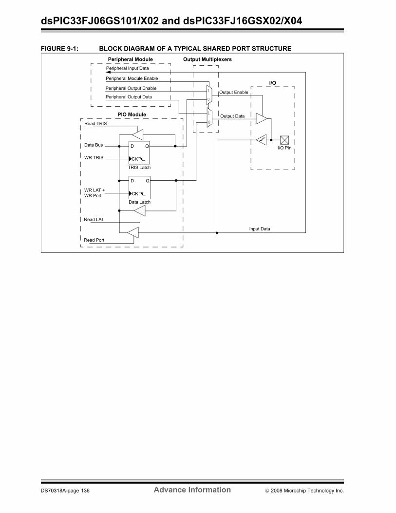
dsPIC33FJ06GS101/X02 and dsPIC33FJ16GSX02/X04
FIGURE 9-1: BLOCK DIAGRAM OF A TYPICAL SHARED PORT STRUCTURE
QD
CK
WR LAT +
TRIS Latch
I/O Pin
WR Port
Data Bus
QD
CK
Data Latch
Read Port
Read TRIS
1
0
1
0
WR TRIS
Peripheral Output DataOutput Enable
Peripheral Input Data
I/O
Peripheral Module
Peripheral Output Enable
PIO Module
Output Multiplexers
Output Data
Input Data
Peripheral Module Enable
Read LAT
DS70318A-page 136 Advance Information © 2008 Microchip Technology Inc.

dsPIC33FJ06GS101/X02 and dsPIC33FJ16GSX02/X04
9.1.1 OPEN-DRAIN CONFIGURATIONIn addition to the PORT, LAT and TRIS registers fordata control, each digital-only port pin can also beindividually configured for either digital or open-drainoutput. This is controlled by the Open-Drain Controlregister, ODCx, associated with each port. Setting anyof the bits configures the corresponding pin to act as anopen-drain output.
The open-drain feature allows the generation ofoutputs higher than VDD (for example, 5V) on anydesired digital-only pins by using external pull-upresistors. The maximum open-drain voltage allowed isthe same as the maximum VIH specification.
9.1.2 5V TOLERANCEAll digital-only pins are 5V tolerant, with the exceptionof the I/O pin, RB5. This pin as well as other analogpins can be operated up to 3.3V only.
9.2 Configuring Analog Port PinsThe ADPCFG and TRIS registers control the operationof the analog-to-digital (A/D) port pins. The port pinsthat are to function as analog inputs must have theircorresponding TRIS bit set (input). If the TRIS bit iscleared (output), the digital output level (VOH or VOL)will be converted.
When the PORT register is read, all pins configured asanalog input channels will read as cleared (a low level).
Pins configured as digital inputs will not convert ananalog input. Analog levels on any pin defined as adigital input (including the ANx pins) can cause theinput buffer to consume current that exceeds thedevice specifications.
9.2.1 I/O PORT WRITE/READ TIMINGOne instruction cycle is required between a port directionchange or port write operation and a read operation ofthe same port. Typically this instruction would be an NOP.An example is shown in Example 9-1.
9.3 Input Change NotificationThe input change notification function of the I/O portsallows the dsPIC33FJ06GS101/X02 anddsPIC33FJ16GSX02/X04 devices to generate interruptrequests to the processor in response to achange-of-state on selected input pins. This featurecan detect input change-of-states even in Sleep mode,when the clocks are disabled. Depending on the devicepin count, up to 30 external signals (CNx pin) can beselected (enabled) for generating an interrupt requeston a change-of-state.
Four control registers are associated with the CNmodule. The CNEN1 and CNEN2 registers contain theinterrupt enable control bits for each of the CN inputpins. Setting any of these bits enables a CN interruptfor the corresponding pins.
Each CN pin also has a weak pull-up connected to it.The pull-ups act as a current source connected to thepin, and eliminate the need for external resistors whenthe push-button or keypad devices are connected. Thepull-ups are enabled separately using the CNPU1 andCNPU2 registers, which contain the control bits foreach of the CN pins. Setting any of the control bitsenables the weak pull-ups for the corresponding pins.
EQUATION 9-1: PORT WRITE/READ EXAMPLE
Note: The I/O pin, RB5, is the only digital pin thatdoes not support open-drain functionality.
Note: Pull-ups on change notification pinsshould always be disabled when the portpin is configured as a digital output.
MOV 0xFF00, W0 ; Configure PORTB<15:8> as inputsMOV W0, TRISBB ; and PORTB<7:0> as outputsNOP ; Delay 1 cyclebtss PORTB, #13 ; Next Instruction
© 2008 Microchip Technology Inc. Advance Information DS70318A-page 137

dsPIC33FJ06GS101/X02 and dsPIC33FJ16GSX02/X04
9.4 Peripheral Pin SelectPeripheral pin select configuration enables peripheralset selection and placement on a wide range of I/Opins. By increasing the pinout options available on aparticular device, programmers can better tailor themicrocontroller to their entire application, rather thantrimming the application to fit the device.
The peripheral pin select configuration featureoperates over a fixed subset of digital I/O pins.Programmers can independently map the input and/oroutput of most digital peripherals to any one of theseI/O pins. Peripheral pin select is performed in software,and generally does not require the device to be repro-grammed. Hardware safeguards are included that pre-vent accidental or spurious changes to the peripheralmapping, once it has been established.
9.4.1 AVAILABLE PINSThe peripheral pin select feature is used with a rangeof up to 30 pins. The number of available pins dependson the particular device and its pin count. Pins thatsupport the peripheral pin select feature include thedesignation “RPn” in their full pin designation, where“RP” designates a remappable peripheral and “n” is theremappable pin number.
9.4.2 AVAILABLE PERIPHERALSThe peripherals managed by the peripheral pin selectfeature are all digital-only peripherals. These include:
• General serial communications (UART and SPI)• General purpose timer clock inputs• Timer-related peripherals (input capture and
output compare)• Interrupt-on-change inputs
In comparison, some digital-only peripheral modulesare never included in the peripheral pin select feature.This is because the peripheral’s function requiresspecial I/O circuitry on a specific port and cannot beeasily connected to multiple pins. These modulesinclude I2C. A similar requirement excludes all moduleswith analog inputs, such as the Analog-to-Digital Con-verter (ADC).
Remappable peripherals are not associated with adefault I/O pin. The peripheral must always beassigned to a specific I/O pin before it can be used. Incontrast, non remappable peripherals are always avail-able on a default pin, assuming that the peripheral isactive and not conflicting with another peripheral.
9.4.2.1 Peripheral Pin Select Function Priority
When a remappable peripheral is active on a given I/Opin, it takes priority over all other digital I/O associatedwith the pin. Priority is given regardless of the type ofperipheral that is mapped. Remappable peripheralsnever take priority over any analog functions associ-ated with the pin.
9.4.3 CONTROLLING PERIPHERAL PIN SELECT
Peripheral pin select features are controlled throughtwo sets of special function registers: one to mapperipheral inputs, and one to map outputs. Becausethey are separately controlled, a particular peripheral’sinput and output (if the peripheral has both) can beplaced on any selectable function pin withoutconstraint.
The association of a peripheral to a peripheral select-able pin is handled in two different ways, depending onwhether an input or output is being mapped.
9.4.3.1 Input MappingThe inputs of the peripheral pin select options aremapped on the basis of the peripheral. A controlregister associated with a peripheral dictates the pin itwill be mapped to. The RPINRx registers are used toconfigure peripheral input mapping (see Register 9-1through Register 9-14). Each register contains sets of6-bit fields, with each set associated with one of theremappable peripherals. Programming a givenperipheral’s bit field with an appropriate 6-bit valuemaps the RPn pin with that value to that peripheral. Forany given device, the valid range of values for any bitfield corresponds to the maximum number of peripheralpin selections supported by the device.
Figure 9-2 Illustrates remappable pin selection forU1RX input.
DS70318A-page 138 Advance Information © 2008 Microchip Technology Inc.

dsPIC33FJ06GS101/X02 and dsPIC33FJ16GSX02/X04
FIGURE 9-2: REMAPPABLE MUX INPUT FOR U1RX
TABLE 9-1: SELECTABLE INPUT SOURCES (MAPS INPUT TO FUNCTION)
Input Name Function Name Register ConfigurationBits
External Interrupt 1 INT1 RPINR0 INT1R<5:0>External Interrupt 2 INT2 RPINR1 INT2R<5:0>Timer 1 External Clock T1CK RPINR2 T1CKR<5:0>Timer 2 External Clock T2CK RPINR3 T2CKR<5:0>Timer 3 External Clock T3CK RPINR3 T3CKR<5:0>Input Capture 1 IC1 RPINR7 IC1R<5:0>Input Capture 2 IC2 RPINR7 IC2R<5:0>Output Compare Fault A OCFA RPINR11 OCFAR<5:0>UART1 Receive U1RX RPINR18 U1RXR<5:0>UART1 Clear To Send U1CTS RPINR18 U1CTSR<5:0>SPI Data Input 1 SDI1 RPINR20 SDI1R<5:0>SPI Clock Input 1 SCK1IN RPINR20 SCK1R<5:0>SPI Slave Select Input 1 SS1IN RPINR21 SS1R<5:0>Fault Input to PWM1 FLT1 RPINR29 FLT1R<5:0>Fault Input to PWM2 FLT2 RPINR30 FLT2R<5:0>Fault Input to PWM3 FLT3 RPINR30 FLT3R<5:0>Fault Input to PWM4 FLT4 RPINR31 FLT4R<5:0>Fault Input to PWM5 FLT5 RPINR31 FLT5R<5:0>Fault Input to PWM6 FLT6 RPINR32 FLT6R<5:0>Fault Input to PWM7 FLT7 RPINR32 FLT7R<5:0>Fault Input to PWM8 FLT8 RPINR33 FLT8R<5:0>External Synchronization signal to PWM Master Time Base SYNCI1 RPINR33 SYNCI1R<5:0>External Synchronization signal to PWM Master Time Base SYNCI2 RPINR34 SYNCI2R<5:0>
RP0
RP1
RP2
RP29
0
29
1
2U1RX input
U1RXR<5:0>
to peripheral
ACMP1ACMP2ACMP3ACMP4
VirtualPins
© 2008 Microchip Technology Inc. Advance Information DS70318A-page 139

dsPIC33FJ06GS101/X02 and dsPIC33FJ16GSX02/X04
9.4.3.2 Virtual Input PinsThe dsPIC33FJ06GS101/X02 anddsPIC33FJ16GSX02/X04 devices’ input remappingfunction supports virtual input pins that are the outputs ofthe internal peripherals. These outputs which are notaccessible to device pins may be of significant use toother peripherals. The remapping logic provides anelegant method that enables inter-peripheral modulecommunication and enhances peripheral modulecapability beyond its initial design goals.
The dsPIC33FJ06GS101/X02 anddsPIC33FJ16GSX02/X04 devices support four virtualpins (ACMP1 - ACMP4) which are the outputs of theanalog comparators and other peripheral modules, suchas the input capture modules or the timer modules.
Traditionally, the peripheral input mapping function isconnected to the RPx pins. The additional inputs tothe multiplexers can be tied to internal nodes withinthe device. These internal nodes are called virtualpins. Different devices provide different virtual pinselections based on the number of peripheralspresent on a device and the advantages of offeringadditional inter-module communication.
9.4.3.3 Output MappingIn contrast to inputs, the outputs of the peripheral pinselect options are mapped on the basis of the pin. Inthis case, a control register associated with a particularpin dictates the peripheral output to be mapped. TheRPORx registers are used to control output mapping.Like the RPINRx registers, each register contains setsof 6-bit fields, with each set associated with one RPnpin (see Register 9-15 through Register 9-27). Thevalue of the bit field corresponds to one of theperipherals, and that peripheral’s output is mapped tothe pin (see Table 9-2 and Figure 9-3).
The list of peripherals for output mapping also includesa null value of 00000 because of the mappingtechnique. This permits any given pin to remainunconnected from the output of any of the pinselectable peripherals.
DS70318A-page 140 Advance Information © 2008 Microchip Technology Inc.

dsPIC33FJ06GS101/X02 and dsPIC33FJ16GSX02/X04
FIGURE 9-3: MULTIPLEXING OF REMAPPABLE OUTPUT FOR RPn
TABLE 9-2: OUTPUT SELECTION FOR REMAPPABLE PIN (RPn) Function RPORn<5:0> Output Name
NULL 000000 RPn tied to default port pinU1TX 000011 RPn tied to UART1 Transmit
U1RTS 000100 RPn tied to UART1 Ready To SendSDO1 000111 RPn tied to SPI1 Data OutputSCK1OUT 001000 RPn tied to SPI1 Clock OutputSS1OUT 001001 RPn tied to SPI1 Slave Select OutputOC1 010010 RPn tied to Output Compare 1OC2 010011 RPn tied to Output Compare 2SYNCO1 100101 RPn tied to External Device Synchronization signal via PWM Master Time BaseREFCLKO 100110 REFCLK output signalACMP1 100111 RPn tied to Analog Comparator Output1ACMP2 101000 RPn tied to Analog Comparator Output2ACMP3 101001 RPn tied to Analog Comparator Output3ACMP4 100010 RPn tied to Analog Comparator Output4PWM4H 101100 RPn tied to PWM output pins associated with PWM Generator 4PWM4L 101101 RPn tied to PWM output pins associated with PWM Generator 4
0
45
3
RPORn<5:0>
default
U1TX Output enable
U1RTS Output enable 4
PWM4L Output enable
19OC2 Output enable
0
45
3
default
U1TX Output
U1RTS Output 4
PWM4L Output19OC2 Output
Output enable
Output DataRPn
© 2008 Microchip Technology Inc. Advance Information DS70318A-page 141

dsPIC33FJ06GS101/X02 and dsPIC33FJ16GSX02/X04
9.4.3.4 Peripheral MappingThe control schema of peripheral select pins is notlimited to a small range of fixed peripheralconfigurations. There are no mutual orhardware-enforced lockouts between any of theperipheral mapping SFRs. Literally any combination ofperipheral mappings across any or all of the RPn pinsis possible. This includes both many-to-one andone-to-many mappings of peripheral inputs andoutputs to pins.
While such mappings may be technically possible froma configuration point of view, they may not besupportable electrically.
9.4.4 CONTROLLING CONFIGURATION CHANGES
Because peripheral remapping can be changed duringrun time, some restrictions on peripheral remappingare needed to prevent accidental configurationchanges. dsPIC33F devices include three features toprevent alterations to the peripheral map:
• Control register lock sequence• Continuous state monitoring• Configuration bit pin select lock
9.4.4.1 Control Register LockUnder normal operation, writes to the RPINRx andRPORx registers are not allowed. Attempted writesappear to execute normally, but the contents of theregisters remain unchanged. To change theseregisters, they must be unlocked in hardware. Theregister lock is controlled by the IOLOCK bit(OSCCON<6>). Setting IOLOCK prevents writes to thecontrol registers; clearing IOLOCK allows writes.
To set or clear IOLOCK, a specific command sequencemust be executed:
1. Write 0x46 to OSCCON<7:0>.2. Write 0x57 to OSCCON<7:0>.3. Clear (or set) IOLOCK as a single operation.
Unlike the similar sequence with the oscillator’s LOCKbit, IOLOCK remains in one state until changed. Thisallows all of the peripheral pin selects to be configuredwith a single unlock sequence followed by an update toall control registers, then locked with a second locksequence.
9.4.4.2 Continuous State MonitoringIn addition to being protected from direct writes, thecontents of the RPINRx and RPORx registers areconstantly monitored in hardware by shadow registers.If an unexpected change in any of the registers occurs(such as cell disturbances caused by ESD or otherexternal events), a configuration mismatch Reset willbe triggered.
9.4.4.3 Configuration Bit Pin Select LockAs an additional level of safety, the device can beconfigured to prevent more than one write session tothe RPINRx and RPORx registers. The IOL1WAY(FOSC<IOL1WAY>) configuration bit blocks theIOLOCK bit from being cleared after it has been setonce. If IOLOCK remains set, the register unlockprocedure will not execute, and the peripheral pinselect control registers cannot be written to. The onlyway to clear the bit and re-enable peripheral remappingis to perform a device Reset.
In the default (unprogrammed) state, IOL1WAY is set,restricting users to one write session. ProgrammingIOL1WAY allows user applications unlimited access(with the proper use of the unlock sequence) to theperipheral pin select registers.
9.4.5 CONSIDERATIONS FOR PERIPHERAL PIN SELECTION
The ability to control peripheral pin selection introducesseveral considerations into application design,including several common peripherals that areavailable only as remappable peripherals.
9.4.5.1 Initialization and LocksThe main consideration is that the peripheral pinselects are not available on default pins in the device’sdefault (Reset) state. More specifically, since allRPINRx registers reset to all 1's and RPORx registersreset to 0's, this means all peripheral pin select inputsare tied to VSS, while all peripheral pin select outputsare disconnected. Therefore, before any otherapplication code is executed, the user application mustinitialize the device with the proper peripheralconfiguration.
Since the IOLOCK bit resets in the unlocked state, it isnot necessary to execute the unlock sequence after thedevice has come out of Reset. For the sake ofapplication safety, however, it is always a good idea toset IOLOCK and lock the configuration after writing tothe control registers.
The unlock sequence must be executed as anassembly-language routine, in the same manner aschanges to the oscillator configuration, because theunlock sequence is timing-critical. If the bulk of theapplication is written in C or another high-levellanguage, the unlock sequence should be performedby writing inline assembler.
Note: MPLAB® C30 provides built-in C languagefunctions for unlocking the OSCCONregister:__builtin_write_OSCCONL(value)__builtin_write_OSCCONH(value)
See MPLAB Help for more information.
DS70318A-page 142 Advance Information © 2008 Microchip Technology Inc.

dsPIC33FJ06GS101/X02 and dsPIC33FJ16GSX02/X04
9.4.5.2 Choosing the ConfigurationChoosing the configuration requires review of allperipheral pin selects and their pin assignments,especially those that will not be used in the application.In all cases, unused pin selectable peripherals shouldbe disabled completely. Unused peripherals shouldhave their inputs assigned to an unused RPn pinfunction. I/O pins with unused RPn functions should beconfigured with the null peripheral output.
The assignment of a peripheral to a particular pin doesnot automatically perform any other configuration of thepin’s I/O circuitry. This means adding a pin selectableoutput to a pin can inadvertently drive an existingperipheral input when the output is driven.Programmers must be familiar with the behavior ofother fixed peripherals that share a remappable pin,and know when to enable or disable them. To be safe,fixed digital peripherals that share the same pin shouldbe disabled when not in use.
9.4.5.3 Pin OperationConfiguring a remappable pin for a specific peripheraldoes not automatically turn that feature on. Theperipheral must be specifically configured for operationand enabled, as if it were tied to a fixed pin. Where thishappens in the application code (immediately followingdevice Reset and peripheral configuration, or inside themain application routine) depends on the peripheraland its use in the application.
9.4.5.4 Analog FunctionsA final consideration is that peripheral pin selectfunctions neither override analog inputs nor reconfigurepins with analog functions for digital I/O. If a pin isconfigured as an analog input on device Reset, it mustbe explicitly reconfigured as digital I/O when used witha peripheral pin select.
9.4.5.5 Configuration ExampleExample 9-1 shows a configuration for bidirectionalcommunication with flow control using UART1. Thefollowing input and output functions are used:
• Input Functions: U1RX, U1CTS• Output Functions: U1TX, U1RTS
EXAMPLE 9-1: CONFIGURING UART1 INPUT AND OUTPUT FUNCTIONS
//*************************************// Unlock Registers//*************************************__builtin_write_OSCCONL(OSCCON & ~(1<<6)); //***************************// Configure Input Functions// (See Table 9-1)//***************************
//***************************// Assign U1Rx To Pin RP0//***************************RPINR18bits.U1RXR = 0;
//***************************// Assign U1CTS To Pin RP1//***************************RPINR18bits.U1CTSR = 1;
//***************************// Configure Output Functions// (See Table 9-2)//***************************
//***************************// Assign U1Tx To Pin RP2//***************************RPOR1bits.RP2R = 3;
//***************************// Assign U1RTS To Pin RP3//***************************RPOR1bits.RP3R = 4;
//*************************************// Lock Registers//*************************************__builtin_write_OSCCONL(OSCCON | (1<<6));
© 2008 Microchip Technology Inc. Advance Information DS70318A-page 143
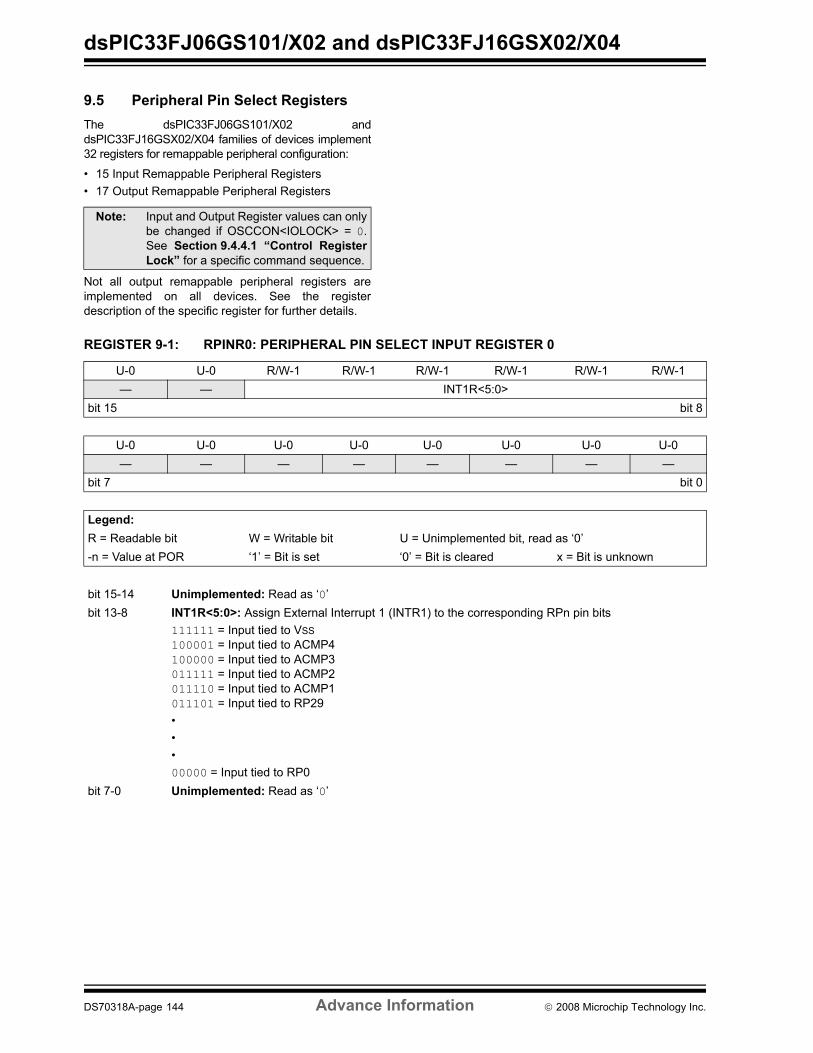
dsPIC33FJ06GS101/X02 and dsPIC33FJ16GSX02/X04
9.5 Peripheral Pin Select RegistersThe dsPIC33FJ06GS101/X02 anddsPIC33FJ16GSX02/X04 families of devices implement32 registers for remappable peripheral configuration:
• 15 Input Remappable Peripheral Registers • 17 Output Remappable Peripheral Registers
Not all output remappable peripheral registers areimplemented on all devices. See the registerdescription of the specific register for further details.
Note: Input and Output Register values can onlybe changed if OSCCON<IOLOCK> = 0.See Section 9.4.4.1 “Control RegisterLock” for a specific command sequence.
REGISTER 9-1: RPINR0: PERIPHERAL PIN SELECT INPUT REGISTER 0
U-0 U-0 R/W-1 R/W-1 R/W-1 R/W-1 R/W-1 R/W-1— — INT1R<5:0>
bit 15 bit 8
U-0 U-0 U-0 U-0 U-0 U-0 U-0 U-0— — — — — — — —
bit 7 bit 0
Legend:R = Readable bit W = Writable bit U = Unimplemented bit, read as ‘0’-n = Value at POR ‘1’ = Bit is set ‘0’ = Bit is cleared x = Bit is unknown
bit 15-14 Unimplemented: Read as ‘0’ bit 13-8 INT1R<5:0>: Assign External Interrupt 1 (INTR1) to the corresponding RPn pin bits
111111 = Input tied to VSS100001 = Input tied to ACMP4100000 = Input tied to ACMP3011111 = Input tied to ACMP2011110 = Input tied to ACMP1011101 = Input tied to RP29•••00000 = Input tied to RP0
bit 7-0 Unimplemented: Read as ‘0’
DS70318A-page 144 Advance Information © 2008 Microchip Technology Inc.
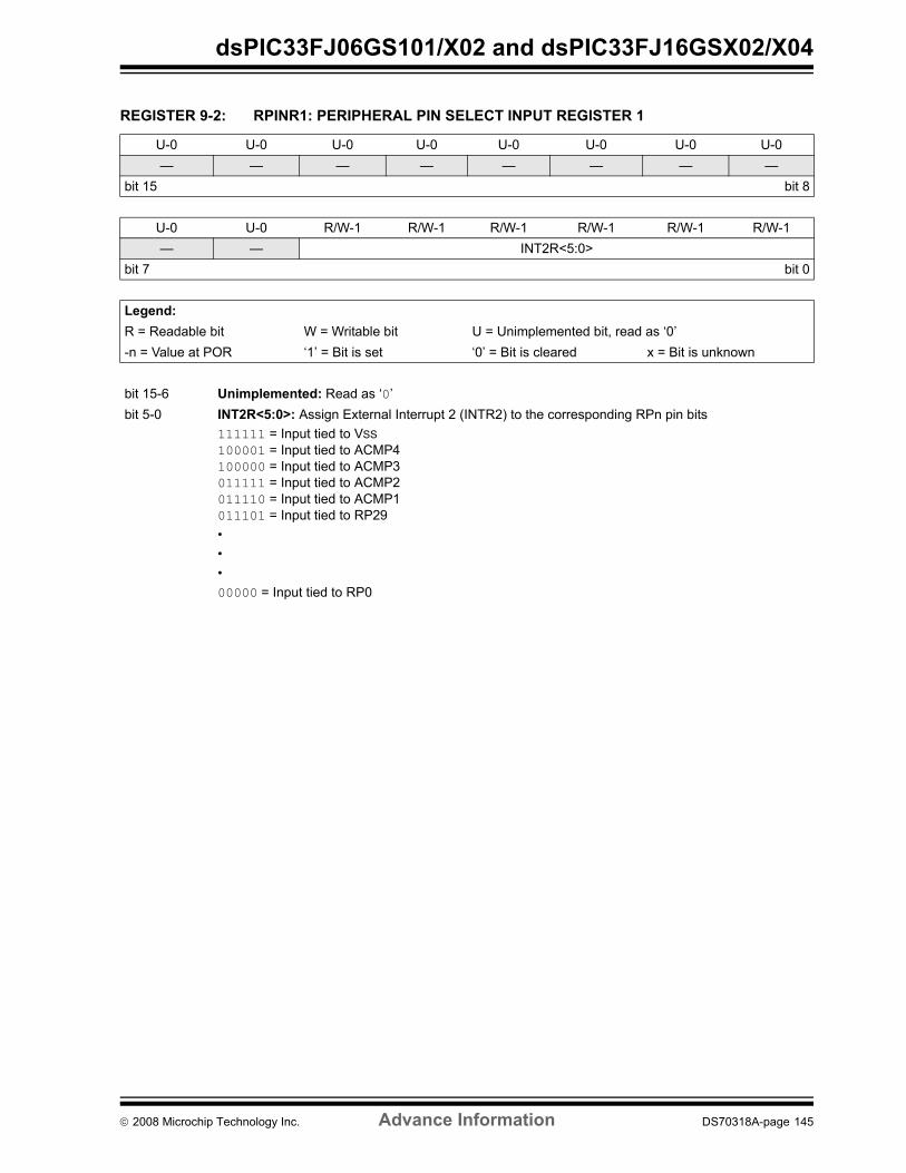
dsPIC33FJ06GS101/X02 and dsPIC33FJ16GSX02/X04
REGISTER 9-2: RPINR1: PERIPHERAL PIN SELECT INPUT REGISTER 1
U-0 U-0 U-0 U-0 U-0 U-0 U-0 U-0— — — — — — — —
bit 15 bit 8
U-0 U-0 R/W-1 R/W-1 R/W-1 R/W-1 R/W-1 R/W-1— — INT2R<5:0>
bit 7 bit 0
Legend:R = Readable bit W = Writable bit U = Unimplemented bit, read as ‘0’-n = Value at POR ‘1’ = Bit is set ‘0’ = Bit is cleared x = Bit is unknown
bit 15-6 Unimplemented: Read as ‘0’ bit 5-0 INT2R<5:0>: Assign External Interrupt 2 (INTR2) to the corresponding RPn pin bits
111111 = Input tied to VSS100001 = Input tied to ACMP4100000 = Input tied to ACMP3011111 = Input tied to ACMP2011110 = Input tied to ACMP1011101 = Input tied to RP29•••00000 = Input tied to RP0
© 2008 Microchip Technology Inc. Advance Information DS70318A-page 145

dsPIC33FJ06GS101/X02 and dsPIC33FJ16GSX02/X04
REGISTER 9-3: RPINR3: PERIPHERAL PIN SELECT INPUT REGISTER 3
U-0 U-0 R/W-1 R/W-1 R/W-1 R/W-1 R/W-1 R/W-1— — T3CKR<5:0>
bit 15 bit 8
U-0 U-0 R/W-1 R/W-1 R/W-1 R/W-1 R/W-1 R/W-1— — T2CKR<5:0>
bit 7 bit 0
Legend:R = Readable bit W = Writable bit U = Unimplemented bit, read as ‘0’-n = Value at POR ‘1’ = Bit is set ‘0’ = Bit is cleared x = Bit is unknown
bit 15-14 Unimplemented: Read as ‘0’ bit 13-8 T3CKR<5:0>: Assign Timer3 External Clock (T3CK) to the corresponding RPn pin bits
111111 = Input tied to VSS100001 = Input tied to ACMP4100000 = Input tied to ACMP3011111 = Input tied to ACMP2011110 = Input tied to ACMP1011101 = Input tied to RP29•••00000 = Input tied to RP0
bit 7-6 Unimplemented: Read as ‘0’ bit 5-0 T2CKR<5:0>: Assign Timer2 External Clock (T2CK) to the corresponding RPn pin bits
111111 = Input tied to VSS100001 = Input tied to ACMP4100000 = Input tied to ACMP3011111 = Input tied to ACMP2011110 = Input tied to ACMP1011101 = Input tied to RP29•••00000 = Input tied to RP0
DS70318A-page 146 Advance Information © 2008 Microchip Technology Inc.

dsPIC33FJ06GS101/X02 and dsPIC33FJ16GSX02/X04
REGISTER 9-4: RPINR7: PERIPHERAL PIN SELECT INPUT REGISTER 7
U-0 U-0 R/W-1 R/W-1 R/W-1 R/W-1 R/W-1 R/W-1— — IC2R<5:0>
bit 15 bit 8
U-0 U-0 R/W-1 R/W-1 R/W-1 R/W-1 R/W-1 R/W-1— — IC1R<5:0>
bit 7 bit 0
Legend:R = Readable bit W = Writable bit U = Unimplemented bit, read as ‘0’-n = Value at POR ‘1’ = Bit is set ‘0’ = Bit is cleared x = Bit is unknown
bit 15-14 Unimplemented: Read as ‘0’ bit 13-8 IC2R<5:0>: Assign Input Capture 2 (IC2) to the corresponding RPn pin bits
111111 = Input tied to VSS100001 = Input tied to ACMP4100000 = Input tied to ACMP3011111 = Input tied to ACMP2011110 = Input tied to ACMP1011101 = Input tied to RP29•••00000 = Input tied to RP0
bit 7-6 Unimplemented: Read as ‘0’ bit 5-0 IC1R<5:0>: Assign Input Capture 1 (IC1) to the corresponding RPn pin bits
111111 = Input tied to VSS100001 = Input tied to ACMP4100000 = Input tied to ACMP3011111 = Input tied to ACMP2011110 = Input tied to ACMP1011101 = Input tied to RP29•••00000 = Input tied to RP0
© 2008 Microchip Technology Inc. Advance Information DS70318A-page 147

dsPIC33FJ06GS101/X02 and dsPIC33FJ16GSX02/X04
REGISTER 9-5: RPINR11: PERIPHERAL PIN SELECT INPUT REGISTER 11
U-0 U-0 R/W-1 R/W-1 R/W-1 R/W-1 R/W-1 R/W-1— — — — — — — —
bit 15 bit 8
U-0 U-0 R/W-1 R/W-1 R/W-1 R/W-1 R/W-1 R/W-1— — OCFAR<5:0>
bit 7 bit 0
Legend:R = Readable bit W = Writable bit U = Unimplemented bit, read as ‘0’-n = Value at POR ‘1’ = Bit is set ‘0’ = Bit is cleared x = Bit is unknown
bit 15-6 Unimplemented: Read as ‘0’ bit 5-0 OCFAR<5:0>: Assign Output Capture A (OCFA) to the corresponding RPn pin bits
111111 = Input tied to VSS100001 = Input tied to ACMP4100000 = Input tied to ACMP3011111 = Input tied to ACMP2011110 = Input tied to ACMP1011101 = Input tied to RP29•••00000 = Input tied to RP0
DS70318A-page 148 Advance Information © 2008 Microchip Technology Inc.
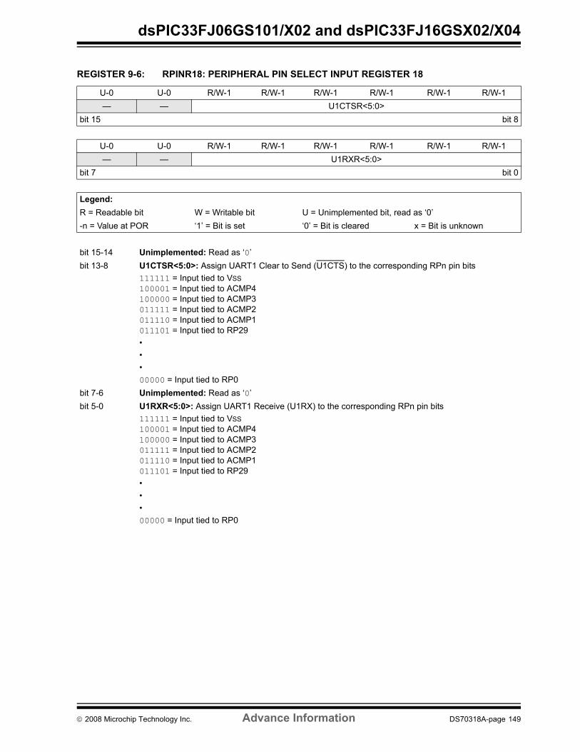
dsPIC33FJ06GS101/X02 and dsPIC33FJ16GSX02/X04
REGISTER 9-6: RPINR18: PERIPHERAL PIN SELECT INPUT REGISTER 18
U-0 U-0 R/W-1 R/W-1 R/W-1 R/W-1 R/W-1 R/W-1— — U1CTSR<5:0>
bit 15 bit 8
U-0 U-0 R/W-1 R/W-1 R/W-1 R/W-1 R/W-1 R/W-1— — U1RXR<5:0>
bit 7 bit 0
Legend:R = Readable bit W = Writable bit U = Unimplemented bit, read as ‘0’-n = Value at POR ‘1’ = Bit is set ‘0’ = Bit is cleared x = Bit is unknown
bit 15-14 Unimplemented: Read as ‘0’ bit 13-8 U1CTSR<5:0>: Assign UART1 Clear to Send (U1CTS) to the corresponding RPn pin bits
111111 = Input tied to VSS100001 = Input tied to ACMP4100000 = Input tied to ACMP3011111 = Input tied to ACMP2011110 = Input tied to ACMP1011101 = Input tied to RP29•••00000 = Input tied to RP0
bit 7-6 Unimplemented: Read as ‘0’ bit 5-0 U1RXR<5:0>: Assign UART1 Receive (U1RX) to the corresponding RPn pin bits
111111 = Input tied to VSS100001 = Input tied to ACMP4100000 = Input tied to ACMP3011111 = Input tied to ACMP2011110 = Input tied to ACMP1011101 = Input tied to RP29•••00000 = Input tied to RP0
© 2008 Microchip Technology Inc. Advance Information DS70318A-page 149

dsPIC33FJ06GS101/X02 and dsPIC33FJ16GSX02/X04
REGISTER 9-7: RPINR20: PERIPHERAL PIN SELECT INPUT REGISTER 20
U-0 U-0 R/W-1 R/W-1 R/W-1 R/W-1 R/W-1 R/W-1— — SCK1R<5:0>
bit 15 bit 8
U-0 U-0 R/W-1 R/W-1 R/W-1 R/W-1 R/W-1 R/W-1— — SDI1R<5:0>
bit 7 bit 0
Legend:R = Readable bit W = Writable bit U = Unimplemented bit, read as ‘0’-n = Value at POR ‘1’ = Bit is set ‘0’ = Bit is cleared x = Bit is unknown
bit 15-14 Unimplemented: Read as ‘0’ bit 13-8 SCK1R<5:0>: Assign SPI1 Clock Input (SCK1IN) to the corresponding RPn pin bits
111111 = Input tied to VSS100001 = Input tied to ACMP4100000 = Input tied to ACMP3011111 = Input tied to ACMP2011110 = Input tied to ACMP1011101 = Input tied to RP29•••00000 = Input tied to RP0
bit 7-6 Unimplemented: Read as ‘0’ bit 5-0 SDI1R<5:0>: Assign SPI1 Data Input (SDI1) to the corresponding RPn pin bits
111111 = Input tied to VSS100001 = Input tied to ACMP4100000 = Input tied to ACMP3011111 = Input tied to ACMP2011110 = Input tied to ACMP1011101 = Input tied to RP29•••00000 = Input tied to RP0
DS70318A-page 150 Advance Information © 2008 Microchip Technology Inc.

dsPIC33FJ06GS101/X02 and dsPIC33FJ16GSX02/X04
REGISTER 9-8: RPINR21: PERIPHERAL PIN SELECT INPUT REGISTER 21
U-0 U-0 U-0 U-0 U-0 U-0 U-0 U-0— — — — — — — —
bit 15 bit 8
U-0 U-0 R/W-1 R/W-1 R/W-1 R/W-1 R/W-1 R/W-1— — SS1R<5:0>
bit 7 bit 0
Legend:R = Readable bit W = Writable bit U = Unimplemented bit, read as ‘0’-n = Value at POR ‘1’ = Bit is set ‘0’ = Bit is cleared x = Bit is unknown
bit 15-6 Unimplemented: Read as ‘0’ bit 5-0 SS1R<5:0>: Assign SPI1 Slave Select Input (SS1IN) to the corresponding RPn pin bits
111111 = Input tied to VSS100001 = Input tied to ACMP4100000 = Input tied to ACMP3011111 = Input tied to ACMP2011110 = Input tied to ACMP1011101 = Input tied to RP29•••00000 = Input tied to RP0
© 2008 Microchip Technology Inc. Advance Information DS70318A-page 151

dsPIC33FJ06GS101/X02 and dsPIC33FJ16GSX02/X04
REGISTER 9-9: RPINR29: PERIPHERAL PIN SELECT INPUT REGISTER 29U-0 U-0 R/W-1 R/W-1 R/W-1 R/W-1 R/W-1 R/W-1— — FLT1R<5:0>
bit 15 bit 8
U-0 U-0 U-0 U-0 U-0 U-0 U-0 U-0— — — — — — — —
bit 7 bit 0
Legend:R = Readable bit W = Writable bit U = Unimplemented bit, read as ‘0’-n = Value at POR ‘1’ = Bit is set ‘0’ = Bit is cleared x = Bit is unknown
bit 15-14 Unimplemented: Read as ‘0’ bit 13-8 FLT1R<5:0>: Assign PWM1Fault input (FLT1) to the corresponding RPn pin bits
111111 = Input tied to VSS100001 = Input tied to ACMP4100000 = Input tied to ACMP3011111 = Input tied to ACMP2011110 = Input tied to ACMP1011101 = Input tied to RP29•••00000 = Input tied to RP0
bit 7-0 Unimplemented: Read as ‘0’
DS70318A-page 152 Advance Information © 2008 Microchip Technology Inc.

dsPIC33FJ06GS101/X02 and dsPIC33FJ16GSX02/X04
REGISTER 9-10: RPINR30: PERIPHERAL PIN SELECT INPUT REGISTER 30U-0 U-0 R/W-1 R/W-1 R/W-1 R/W-1 R/W-1 R/W-1— — FLT3R<5:0>
bit 15 bit 8
U-0 U-0 R/W-1 R/W-1 R/W-1 R/W-1 R/W-1 R/W-1— — FLT2R<5:0>
bit 7 bit 0
Legend:R = Readable bit W = Writable bit U = Unimplemented bit, read as ‘0’-n = Value at POR ‘1’ = Bit is set ‘0’ = Bit is cleared x = Bit is unknown
bit 15-14 Unimplemented: Read as ‘0’ bit 13-8 FLT3R<5:0>: Assign PWM3 Fault input (FLT3) to the corresponding RPn pin bits
111111 = Input tied to VSS100001 = Input tied to ACMP4100000 = Input tied to ACMP3011111 = Input tied to ACMP2011110 = Input tied to ACMP1011101 = Input tied to RP29•••00000 = Input tied to RP0
bit 7-6 Unimplemented: Read as ‘0’ bit 5-0 FLT2R<5:0>: Assign PWM2 Fault input (FLT2) to the corresponding RPn pin bits
111111 = Input tied to VSS100001 = Input tied to ACMP4100000 = Input tied to ACMP3011111 = Input tied to ACMP2011110 = Input tied to ACMP1011101 = Input tied to RP29•••00000 = Input tied to RP0
© 2008 Microchip Technology Inc. Advance Information DS70318A-page 153

dsPIC33FJ06GS101/X02 and dsPIC33FJ16GSX02/X04
REGISTER 9-11: RPINR31: PERIPHERAL PIN SELECT INPUT REGISTER 31U-0 U-0 R/W-1 R/W-1 R/W-1 R/W-1 R/W-1 R/W-1— — FLT5R<5:0>
bit 15 bit 8
U-0 U-0 R/W-1 R/W-1 R/W-1 R/W-1 R/W-1 R/W-1— — FLT4R<5:0>
bit 7 bit 0
Legend:R = Readable bit W = Writable bit U = Unimplemented bit, read as ‘0’-n = Value at POR ‘1’ = Bit is set ‘0’ = Bit is cleared x = Bit is unknown
bit 15-14 Unimplemented: Read as ‘0’ bit 13-8 FLT5R<5:0>: Assign PWM5 Fault input (FLT5) to the corresponding RPn pin bits
111111 = Input tied to VSS100001 = Input tied to ACMP4100000 = Input tied to ACMP3011111 = Input tied to ACMP2011110 = Input tied to ACMP1011101 = Input tied to RP29•••00000 = Input tied to RP0
bit 7-6 Unimplemented: Read as ‘0’ bit 5-0 FLT4R<5:0>: Assign PWM4 Fault input (FLT4) to the corresponding RPn pin bits
111111 = Input tied to VSS100001 = Input tied to ACMP4100000 = Input tied to ACMP3011111 = Input tied to ACMP2011110 = Input tied to ACMP1011101 = Input tied to RP29•••00000 = Input tied to RP0
DS70318A-page 154 Advance Information © 2008 Microchip Technology Inc.
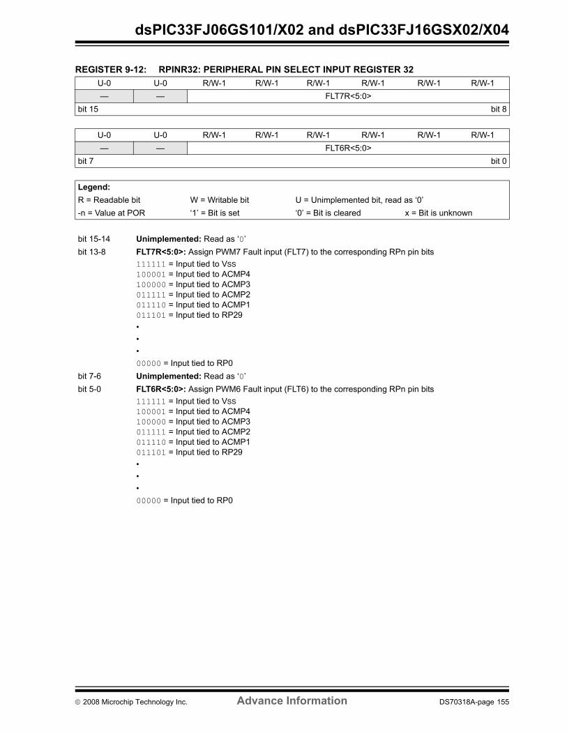
dsPIC33FJ06GS101/X02 and dsPIC33FJ16GSX02/X04
REGISTER 9-12: RPINR32: PERIPHERAL PIN SELECT INPUT REGISTER 32U-0 U-0 R/W-1 R/W-1 R/W-1 R/W-1 R/W-1 R/W-1— — FLT7R<5:0>
bit 15 bit 8
U-0 U-0 R/W-1 R/W-1 R/W-1 R/W-1 R/W-1 R/W-1— — FLT6R<5:0>
bit 7 bit 0
Legend:R = Readable bit W = Writable bit U = Unimplemented bit, read as ‘0’-n = Value at POR ‘1’ = Bit is set ‘0’ = Bit is cleared x = Bit is unknown
bit 15-14 Unimplemented: Read as ‘0’ bit 13-8 FLT7R<5:0>: Assign PWM7 Fault input (FLT7) to the corresponding RPn pin bits
111111 = Input tied to VSS100001 = Input tied to ACMP4100000 = Input tied to ACMP3011111 = Input tied to ACMP2011110 = Input tied to ACMP1011101 = Input tied to RP29•••00000 = Input tied to RP0
bit 7-6 Unimplemented: Read as ‘0’ bit 5-0 FLT6R<5:0>: Assign PWM6 Fault input (FLT6) to the corresponding RPn pin bits
111111 = Input tied to VSS100001 = Input tied to ACMP4100000 = Input tied to ACMP3011111 = Input tied to ACMP2011110 = Input tied to ACMP1011101 = Input tied to RP29•••00000 = Input tied to RP0
© 2008 Microchip Technology Inc. Advance Information DS70318A-page 155

dsPIC33FJ06GS101/X02 and dsPIC33FJ16GSX02/X04
REGISTER 9-13: RPINR33: PERIPHERAL PIN SELECT INPUT REGISTER 33U-0 U-0 R/W-1 R/W-1 R/W-1 R/W-1 R/W-1 R/W-1— — SYNCI1R<5:0>
bit 15 bit 8
U-0 U-0 R/W-1 R/W-1 R/W-1 R/W-1 R/W-1 R/W-1— — FLT8R<5:0>
bit 7 bit 0
Legend:R = Readable bit W = Writable bit U = Unimplemented bit, read as ‘0’-n = Value at POR ‘1’ = Bit is set ‘0’ = Bit is cleared x = Bit is unknown
bit 15-14 Unimplemented: Read as ‘0’ bit 13-8 SYNCI1R<5:0>: Assign PWM Master Time Base External Synchronization signal to the correspond-
ing RPn pin bits111111 = Input tied to VSS100001 = Input tied to ACMP4100000 = Input tied to ACMP3011111 = Input tied to ACMP2011110 = Input tied to ACMP1011101 = Input tied to RP29•••00000 = Input tied to RP0
bit 7-6 Unimplemented: Read as ‘0’ bit 5-0 FLT8R<5:0>: Assign PWM8 Fault input (FLT8) to the corresponding RPn pin bits
111111 = Input tied to VSS100001 = Input tied to ACMP4100000 = Input tied to ACMP3011111 = Input tied to ACMP2011110 = Input tied to ACMP1011101 = Input tied to RP29•••00000 = Input tied to RP0
DS70318A-page 156 Advance Information © 2008 Microchip Technology Inc.

dsPIC33FJ06GS101/X02 and dsPIC33FJ16GSX02/X04
REGISTER 9-14: RPINR34: PERIPHERAL PIN SELECT INPUT REGISTER 34U-0 U-0 U-0 U-0 U-0 U-0 U-0 U-0— — — — — — — —
bit 15 bit 8
U-0 U-0 R/W-1 R/W-1 R/W-1 R/W-1 R/W-1 R/W-1— — SYNCI2R<5:0>
bit 7 bit 0
Legend:R = Readable bit W = Writable bit U = Unimplemented bit, read as ‘0’-n = Value at POR ‘1’ = Bit is set ‘0’ = Bit is cleared x = Bit is unknown
bit 15-6 Unimplemented: Read as ‘0’ bit 5-0 SYNCI2R<5:0>: Assign PWM Master Time Base External Synchronization signal to the correspond-
ing RPn pin bits111111 = Input tied to VSS100001 = Input tied to ACMP4100000 = Input tied to ACMP3011111 = Input tied to ACMP2011110 = Input tied to ACMP1011101 = Input tied to RP29•••00000 = Input tied to RP0
REGISTER 9-15: RPOR0: PERIPHERAL PIN SELECT OUTPUT REGISTERS 0
U-0 U-0 R/W-0 R/W-0 R/W-0 R/W-0 R/W-0 R/W-0— — RP1R<5:0>
bit 15 bit 8
U-0 U-0 R/W-0 R/W-0 R/W-0 R/W-0 R/W-0 R/W-0— — RP0R<5:0>
bit 7 bit 0
Legend:R = Readable bit W = Writable bit U = Unimplemented bit, read as ‘0’-n = Value at POR ‘1’ = Bit is set ‘0’ = Bit is cleared x = Bit is unknown
bit 15-14 Unimplemented: Read as ‘0’ bit 13-8 RP1R<5:0>: Peripheral Output Function is Assigned to RP1 Output Pin bits (see Table 9-2 for
peripheral function numbers)bit 7-6 Unimplemented: Read as ‘0’ bit 5-0 RP0R<5:0>: Peripheral Output Function is Assigned to RP0 Output Pin bits (see Table 9-2 for
peripheral function numbers)
© 2008 Microchip Technology Inc. Advance Information DS70318A-page 157

dsPIC33FJ06GS101/X02 and dsPIC33FJ16GSX02/X04
REGISTER 9-16: RPOR1: PERIPHERAL PIN SELECT OUTPUT REGISTERS 1
U-0 U-0 R/W-0 R/W-0 R/W-0 R/W-0 R/W-0 R/W-0— — RP3R<5:0>
bit 15 bit 8
U-0 U-0 R/W-0 R/W-0 R/W-0 R/W-0 R/W-0 R/W-0— — RP2R<5:0>
bit 7 bit 0
Legend:R = Readable bit W = Writable bit U = Unimplemented bit, read as ‘0’-n = Value at POR ‘1’ = Bit is set ‘0’ = Bit is cleared x = Bit is unknown
bit 15-14 Unimplemented: Read as ‘0’ bit 13-8 RP3R<5:0>: Peripheral Output Function is Assigned to RP3 Output Pin bits (see Table 9-2 for
peripheral function numbers)bit 7-6 Unimplemented: Read as ‘0’ bit 5-0 RP2R<5:0>: Peripheral Output Function is Assigned to RP2 Output Pin bits (see Table 9-2 for
peripheral function numbers)
REGISTER 9-17: RPOR2: PERIPHERAL PIN SELECT OUTPUT REGISTERS 2
U-0 U-0 R/W-0 R/W-0 R/W-0 R/W-0 R/W-0 R/W-0— — RP5R<5:0>
bit 15 bit 8
U-0 U-0 R/W-0 R/W-0 R/W-0 R/W-0 R/W-0 R/W-0— — RP4R<5:0>
bit 7 bit 0
Legend:R = Readable bit W = Writable bit U = Unimplemented bit, read as ‘0’-n = Value at POR ‘1’ = Bit is set ‘0’ = Bit is cleared x = Bit is unknown
bit 15-14 Unimplemented: Read as ‘0’ bit 13-8 RP5R<5:0>: Peripheral Output Function is Assigned to RP5 Output Pin bits (see Table 9-2 for
peripheral function numbers)bit 7-6 Unimplemented: Read as ‘0’ bit 5-0 RP4R<5:0>: Peripheral Output Function is Assigned to RP4 Output Pin bits (see Table 9-2 for
peripheral function numbers)
DS70318A-page 158 Advance Information © 2008 Microchip Technology Inc.

dsPIC33FJ06GS101/X02 and dsPIC33FJ16GSX02/X04
REGISTER 9-18: RPOR3: PERIPHERAL PIN SELECT OUTPUT REGISTERS 3
U-0 U-0 R/W-0 R/W-0 R/W-0 R/W-0 R/W-0 R/W-0— — RP7R<5:0>
bit 15 bit 8
U-0 U-0 R/W-0 R/W-0 R/W-0 R/W-0 R/W-0 R/W-0— — RP6R<5:0>
bit 7 bit 0
Legend:R = Readable bit W = Writable bit U = Unimplemented bit, read as ‘0’-n = Value at POR ‘1’ = Bit is set ‘0’ = Bit is cleared x = Bit is unknown
bit 15-14 Unimplemented: Read as ‘0’ bit 13-8 RP7R<5:0>: Peripheral Output Function is Assigned to RP7 Output Pin bits (see Table 9-2 for
peripheral function numbers)bit 7-6 Unimplemented: Read as ‘0’ bit 5-0 RP6R<5:0>: Peripheral Output Function is Assigned to RP6 Output Pin bits (see Table 9-2 for
peripheral function numbers)
REGISTER 9-19: RPOR4: PERIPHERAL PIN SELECT OUTPUT REGISTERS 4
U-0 U-0 R/W-0 R/W-0 R/W-0 R/W-0 R/W-0 R/W-0— — RP9R<5:0>
bit 15 bit 8
U-0 U-0 R/W-0 R/W-0 R/W-0 R/W-0 R/W-0 R/W-0— — RP8R<5:0>
bit 7 bit 0
Legend:R = Readable bit W = Writable bit U = Unimplemented bit, read as ‘0’-n = Value at POR ‘1’ = Bit is set ‘0’ = Bit is cleared x = Bit is unknown
bit 15-14 Unimplemented: Read as ‘0’ bit 13-8 RP9R<5:0>: Peripheral Output Function is Assigned to RP9 Output Pin bits (see Table 9-2 for
peripheral function numbers)bit 7-6 Unimplemented: Read as ‘0’ bit 5-0 RP8R<5:0>: Peripheral Output Function is Assigned to RP8 Output Pin bits (see Table 9-2 for
peripheral function numbers)
Note 1: This register is not implemented in dsPIC33FJ06GS101 device.
© 2008 Microchip Technology Inc. Advance Information DS70318A-page 159

dsPIC33FJ06GS101/X02 and dsPIC33FJ16GSX02/X04
REGISTER 9-20: RPOR5: PERIPHERAL PIN SELECT OUTPUT REGISTERS 5
U-0 U-0 R/W-0 R/W-0 R/W-0 R/W-0 R/W-0 R/W-0— — RP11R<5:0>
bit 15 bit 8
U-0 U-0 R/W-0 R/W-0 R/W-0 R/W-0 R/W-0 R/W-0— — RP10R<5:0>
bit 7 bit 0
Legend:R = Readable bit W = Writable bit U = Unimplemented bit, read as ‘0’-n = Value at POR ‘1’ = Bit is set ‘0’ = Bit is cleared x = Bit is unknown
bit 15-14 Unimplemented: Read as ‘0’ bit 13-8 RP11R<5:0>: Peripheral Output Function is Assigned to RP11 Output Pin bits (see Table 9-2 for
peripheral function numbers)bit 7-6 Unimplemented: Read as ‘0’ bit 5-0 RP10R<5:0>: Peripheral Output Function is Assigned to RP10 Output Pin bits (see Table 9-2 for
peripheral function numbers)
Note 1: This register is not implemented in dsPIC33FJ06GS101 device.
REGISTER 9-21: RPOR6: PERIPHERAL PIN SELECT OUTPUT REGISTERS 6
U-0 U-0 R/W-0 R/W-0 R/W-0 R/W-0 R/W-0 R/W-0— — RP13R<5:0>
bit 15 bit 8
U-0 U-0 R/W-0 R/W-0 R/W-0 R/W-0 R/W-0 R/W-0— — RP12R<5:0>
bit 7 bit 0
Legend:R = Readable bit W = Writable bit U = Unimplemented bit, read as ‘0’-n = Value at POR ‘1’ = Bit is set ‘0’ = Bit is cleared x = Bit is unknown
bit 15-14 Unimplemented: Read as ‘0’ bit 13-8 RP13R<5:0>: Peripheral Output Function is Assigned to RP13 Output Pin bits (see Table 9-2 for
peripheral function numbers)bit 7-6 Unimplemented: Read as ‘0’ bit 5-0 RP12R<5:0>: Peripheral Output Function is Assigned to RP12 Output Pin bits (see Table 9-2 for
peripheral function numbers)
Note 1: This register is not implemented in dsPIC33FJ06GS101 device.
DS70318A-page 160 Advance Information © 2008 Microchip Technology Inc.
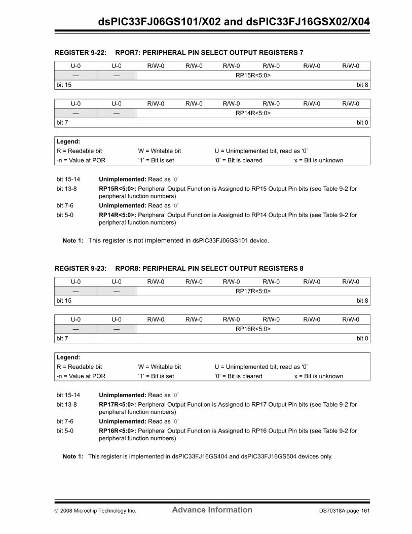
dsPIC33FJ06GS101/X02 and dsPIC33FJ16GSX02/X04
REGISTER 9-22: RPOR7: PERIPHERAL PIN SELECT OUTPUT REGISTERS 7
U-0 U-0 R/W-0 R/W-0 R/W-0 R/W-0 R/W-0 R/W-0— — RP15R<5:0>
bit 15 bit 8
U-0 U-0 R/W-0 R/W-0 R/W-0 R/W-0 R/W-0 R/W-0— — RP14R<5:0>
bit 7 bit 0
Legend:R = Readable bit W = Writable bit U = Unimplemented bit, read as ‘0’-n = Value at POR ‘1’ = Bit is set ‘0’ = Bit is cleared x = Bit is unknown
bit 15-14 Unimplemented: Read as ‘0’ bit 13-8 RP15R<5:0>: Peripheral Output Function is Assigned to RP15 Output Pin bits (see Table 9-2 for
peripheral function numbers)bit 7-6 Unimplemented: Read as ‘0’ bit 5-0 RP14R<5:0>: Peripheral Output Function is Assigned to RP14 Output Pin bits (see Table 9-2 for
peripheral function numbers)
Note 1: This register is not implemented in dsPIC33FJ06GS101 device.
REGISTER 9-23: RPOR8: PERIPHERAL PIN SELECT OUTPUT REGISTERS 8
U-0 U-0 R/W-0 R/W-0 R/W-0 R/W-0 R/W-0 R/W-0— — RP17R<5:0>
bit 15 bit 8
U-0 U-0 R/W-0 R/W-0 R/W-0 R/W-0 R/W-0 R/W-0— — RP16R<5:0>
bit 7 bit 0
Legend:R = Readable bit W = Writable bit U = Unimplemented bit, read as ‘0’-n = Value at POR ‘1’ = Bit is set ‘0’ = Bit is cleared x = Bit is unknown
bit 15-14 Unimplemented: Read as ‘0’ bit 13-8 RP17R<5:0>: Peripheral Output Function is Assigned to RP17 Output Pin bits (see Table 9-2 for
peripheral function numbers)bit 7-6 Unimplemented: Read as ‘0’ bit 5-0 RP16R<5:0>: Peripheral Output Function is Assigned to RP16 Output Pin bits (see Table 9-2 for
peripheral function numbers)
Note 1: This register is implemented in dsPIC33FJ16GS404 and dsPIC33FJ16GS504 devices only.
© 2008 Microchip Technology Inc. Advance Information DS70318A-page 161
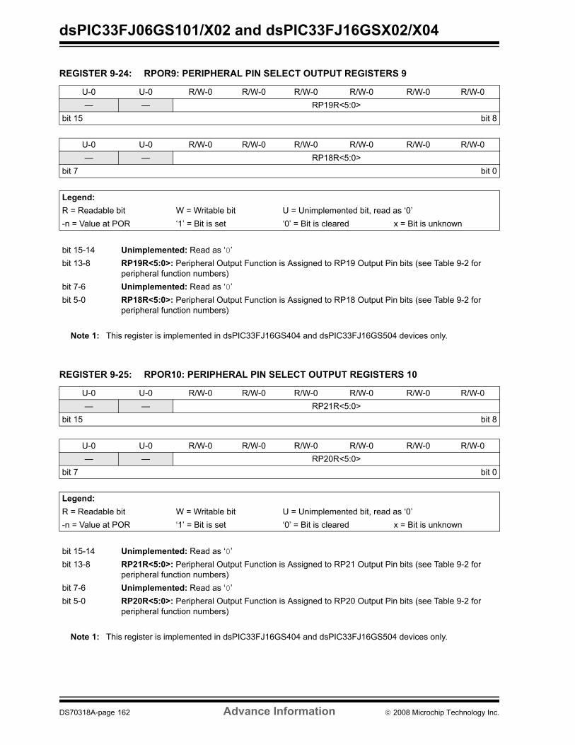
dsPIC33FJ06GS101/X02 and dsPIC33FJ16GSX02/X04
REGISTER 9-24: RPOR9: PERIPHERAL PIN SELECT OUTPUT REGISTERS 9
U-0 U-0 R/W-0 R/W-0 R/W-0 R/W-0 R/W-0 R/W-0— — RP19R<5:0>
bit 15 bit 8
U-0 U-0 R/W-0 R/W-0 R/W-0 R/W-0 R/W-0 R/W-0— — RP18R<5:0>
bit 7 bit 0
Legend:R = Readable bit W = Writable bit U = Unimplemented bit, read as ‘0’-n = Value at POR ‘1’ = Bit is set ‘0’ = Bit is cleared x = Bit is unknown
bit 15-14 Unimplemented: Read as ‘0’ bit 13-8 RP19R<5:0>: Peripheral Output Function is Assigned to RP19 Output Pin bits (see Table 9-2 for
peripheral function numbers)bit 7-6 Unimplemented: Read as ‘0’ bit 5-0 RP18R<5:0>: Peripheral Output Function is Assigned to RP18 Output Pin bits (see Table 9-2 for
peripheral function numbers)
Note 1: This register is implemented in dsPIC33FJ16GS404 and dsPIC33FJ16GS504 devices only.
REGISTER 9-25: RPOR10: PERIPHERAL PIN SELECT OUTPUT REGISTERS 10
U-0 U-0 R/W-0 R/W-0 R/W-0 R/W-0 R/W-0 R/W-0— — RP21R<5:0>
bit 15 bit 8
U-0 U-0 R/W-0 R/W-0 R/W-0 R/W-0 R/W-0 R/W-0— — RP20R<5:0>
bit 7 bit 0
Legend:R = Readable bit W = Writable bit U = Unimplemented bit, read as ‘0’-n = Value at POR ‘1’ = Bit is set ‘0’ = Bit is cleared x = Bit is unknown
bit 15-14 Unimplemented: Read as ‘0’ bit 13-8 RP21R<5:0>: Peripheral Output Function is Assigned to RP21 Output Pin bits (see Table 9-2 for
peripheral function numbers)bit 7-6 Unimplemented: Read as ‘0’ bit 5-0 RP20R<5:0>: Peripheral Output Function is Assigned to RP20 Output Pin bits (see Table 9-2 for
peripheral function numbers)
Note 1: This register is implemented in dsPIC33FJ16GS404 and dsPIC33FJ16GS504 devices only.
DS70318A-page 162 Advance Information © 2008 Microchip Technology Inc.

dsPIC33FJ06GS101/X02 and dsPIC33FJ16GSX02/X04
REGISTER 9-26: RPOR11: PERIPHERAL PIN SELECT OUTPUT REGISTERS 11
U-0 U-0 R/W-0 R/W-0 R/W-0 R/W-0 R/W-0 R/W-0— — RP23R<5:0>
bit 15 bit 8
U-0 U-0 R/W-0 R/W-0 R/W-0 R/W-0 R/W-0 R/W-0— — RP22R<5:0>
bit 7 bit 0
Legend:R = Readable bit W = Writable bit U = Unimplemented bit, read as ‘0’-n = Value at POR ‘1’ = Bit is set ‘0’ = Bit is cleared x = Bit is unknown
bit 15-14 Unimplemented: Read as ‘0’ bit 13-8 RP23R<5:0>: Peripheral Output Function is Assigned to RP23 Output Pin bits (see Table 9-2 for
peripheral function numbers)bit 7-6 Unimplemented: Read as ‘0’ bit 5-0 RP22R<5:0>: Peripheral Output Function is Assigned to RP22 Output Pin bits (see Table 9-2 for
peripheral function numbers)
Note 1: This register is implemented in dsPIC33FJ16GS404 and dsPIC33FJ16GS504 devices only.
REGISTER 9-27: RPOR12: PERIPHERAL PIN SELECT OUTPUT REGISTERS 12
U-0 U-0 R/W-0 R/W-0 R/W-0 R/W-0 R/W-0 R/W-0— — RP25R<5:0>
bit 15 bit 8
U-0 U-0 R/W-0 R/W-0 R/W-0 R/W-0 R/W-0 R/W-0— — RP24R<5:0>
bit 7 bit 0
Legend:R = Readable bit W = Writable bit U = Unimplemented bit, read as ‘0’-n = Value at POR ‘1’ = Bit is set ‘0’ = Bit is cleared x = Bit is unknown
bit 15-14 Unimplemented: Read as ‘0’ bit 13-8 RP25R<5:0>: Peripheral Output Function is Assigned to RP25 Output Pin bits (see Table 9-2 for
peripheral function numbers)bit 7-6 Unimplemented: Read as ‘0’ bit 5-0 RP24R<5:0>: Peripheral Output Function is Assigned to RP24 Output Pin bits (see Table 9-2 for
peripheral function numbers)
Note 1: This register is implemented in dsPIC33FJ16GS404 and dsPIC33FJ16GS504 devices only.
© 2008 Microchip Technology Inc. Advance Information DS70318A-page 163

dsPIC33FJ06GS101/X02 and dsPIC33FJ16GSX02/X04
REGISTER 9-28: RPOR13: PERIPHERAL PIN SELECT OUTPUT REGISTERS 13
REGISTER 9-29: RPOR14: PERIPHERAL PIN SELECT OUTPUT REGISTERS 14
U-0 U-0 R/W-0 R/W-0 R/W-0 R/W-0 R/W-0 R/W-0— — RP27R<5:0>
bit 15 bit 8
U-0 U-0 R/W-0 R/W-0 R/W-0 R/W-0 R/W-0 R/W-0— — RP26R<5:0>
bit 7 bit 0
Legend:R = Readable bit W = Writable bit U = Unimplemented bit, read as ‘0’-n = Value at POR ‘1’ = Bit is set ‘0’ = Bit is cleared x = Bit is unknown
bit 15-14 Unimplemented: Read as ‘0’ bit 13-8 RP27R<5:0>: Peripheral Output Function is Assigned to RP27 Output Pin bits (see Table 9-2 for
peripheral function numbers)bit 7-6 Unimplemented: Read as ‘0’ bit 5-0 RP26R<5:0>: Peripheral Output Function is Assigned to RP26 Output Pin bits (see Table 9-2 for
peripheral function numbers)
Note 1: This register is implemented in dsPIC33FJ16GS404 and dsPIC33FJ16GS504 devices only.
U-0 U-0 R/W-0 R/W-0 R/W-0 R/W-0 R/W-0 R/W-0— — RP29R<5:0>
bit 15 bit 8
U-0 U-0 R/W-0 R/W-0 R/W-0 R/W-0 R/W-0 R/W-0— — RP28R<5:0>
bit 7 bit 0
Legend:R = Readable bit W = Writable bit U = Unimplemented bit, read as ‘0’-n = Value at POR ‘1’ = Bit is set ‘0’ = Bit is cleared x = Bit is unknown
bit 15-14 Unimplemented: Read as ‘0’ bit 13-8 RP29R<5:0>: Peripheral Output Function is Assigned to RP29 Output Pin bits (see Table 9-2 for
peripheral function numbers)bit 7-6 Unimplemented: Read as ‘0’ bit 5-0 RP28R<5:0>: Peripheral Output Function is Assigned to RP28 Output Pin bits (see Table 9-2 for
peripheral function numbers)
Note 1: This register is implemented in dsPIC33FJ16GS404 and dsPIC33FJ16GS504 devices only.
DS70318A-page 164 Advance Information © 2008 Microchip Technology Inc.

dsPIC33FJ06GS101/X02 and dsPIC33FJ16GSX02/X04
10.0 TIMER1
The Timer1 module is a 16-bit timer, which can serveas a time counter for the real-time clock, or operate asa free-running interval timer/counter.
The Timer1 module has the following unique featuresover other timers:
• Can be operated from the low power 32 kHz crystal oscillator available on the device
• Can be operated in Asynchronous Counter mode from an external clock source.
• The external clock input (T1CK) can optionally be synchronized to the internal device clock and the clock synchronization is performed after the prescaler.
The unique features of Timer1 allow it to be used forReal Time Clock (RTC) applications. A block diagramof Timer1 is shown in Figure 10-1.
The Timer1 module can operate in one of the followingmodes:
• Timer mode• Gated Timer mode• Synchronous Counter mode• Asynchronous Counter mode
In Timer and Gated Timer modes, the input clock isderived from the internal instruction cycle clock (FCY).In Synchronous and Asynchronous Counter modes,the input clock is derived from the external clock inputat the T1CK pin.
The Timer modes are determined by the following bits:
• Timer Clock Source Control bit (TCS): T1CON<1>• Timer Synchronization Control bit (TSYNC):
T1CON<2>• Timer Gate Control bit (TGATE): T1CON<6>
Timer control bit setting for different operating modesare given in the Table 10-1.
TABLE 10-1: TIMER MODE SETTINGS
FIGURE 10-1: 16-BIT TIMER1 MODULE BLOCK DIAGRAM
Note: This data sheet summarizes the featuresof the dsPIC33FJ06GS101/X02 anddsPIC33FJ16GSX02/X04 families ofdevices. It is not intended to be acomprehensive reference source. Tocomplement the information in this datasheet, refer to the dsPIC33F FamilyReference Manual, “Section 11. Timers”(DS70205), which is available from theMicrochip website (www.microchip.com).
Mode TCS TGATE TSYNC
Timer 0 0 x
Gated timer 0 1 x
Synchronous counter
1 x 1
Asynchronous counter
1 x 0
TGATE
TCS
00
10
x1
TMR1
Comparator
PR1
TGATE
Set T1IF flag
0
1
TSYNC
0
1
SyncEqual
Reset
T1CKPrescaler
(/n)
TCKPS<1:0>
GateSync
FCY
Falling Edge Detect
Prescaler(/n)
TCKPS<1:0>
© 2008 Microchip Technology Inc. Advance Information DS70318A-page 165

dsPIC33FJ06GS101/X02 and dsPIC33FJ16GSX02/X04
REGISTER 10-1: T1CON: TIMER1 CONTROL REGISTER
R/W-0 U-0 R/W-0 U-0 U-0 U-0 U-0 U-0TON — TSIDL — — — — —
bit 15 bit 8
U-0 R/W-0 R/W-0 R/W-0 U-0 R/W-0 R/W-0 U-0— TGATE TCKPS<1:0> — TSYNC TCS —
bit 7 bit 0
Legend:R = Readable bit W = Writable bit U = Unimplemented bit, read as ‘0’-n = Value at POR ‘1’ = Bit is set ‘0’ = Bit is cleared x = Bit is unknown
bit 15 TON: Timer1 On bit1 = Starts 16-bit Timer10 = Stops 16-bit Timer1
bit 14 Unimplemented: Read as ‘0’bit 13 TSIDL: Stop in Idle Mode bit
1 = Discontinue module operation when device enters Idle mode0 = Continue module operation in Idle mode
bit 12-7 Unimplemented: Read as ‘0’bit 6 TGATE: Timer1 Gated Time Accumulation Enable bit
When T1CS = 1: This bit is ignored.When T1CS = 0: 1 = Gated time accumulation enabled0 = Gated time accumulation disabled
bit 5-4 TCKPS<1:0> Timer1 Input Clock Prescale Select bits11 = 1:256 10 = 1:6401 = 1:8 00 = 1:1
bit 3 Unimplemented: Read as ‘0’bit 2 TSYNC: Timer1 External Clock Input Synchronization Select bit
When TCS = 1: 1 = Synchronize external clock input0 = Do not synchronize external clock inputWhen TCS = 0: This bit is ignored.
bit 1 TCS: Timer1 Clock Source Select bit1 = External clock from pin T1CK (on the rising edge) 0 = Internal clock (FCY)
bit 0 Unimplemented: Read as ‘0’
DS70318A-page 166 Advance Information © 2008 Microchip Technology Inc.

dsPIC33FJ06GS101/X02 and dsPIC33FJ16GSX02/X04
11.0 TIMER2/3 FEATURES
Timer2 is a Type B timer that offers the following majorfeatures:
• A Type B timer can be concatenated with a Type C timer to form a 32-bit timer
• External clock input (TxCK) is always synchronized to the internal device clock and the clock
synchronization is performed after the prescaler. Figure 11-1 shows a block diagram of the Type B timer. Timer3 is a Type C timer that offers the following majorfeatures:• A Type C timer can be concatenated with a Type
B timer to form a 32-bit timer• At least one Type C timer has the ability to trigger
an A/D conversion.• The external clock input (TxCK) is always
synchronized to the internal device clock and the clock synchronization is performed before the prescaler
A block diagram of the Type C timer is shown inFigure 11-2.
FIGURE 11-1: TYPE B TIMER BLOCK DIAGRAM (x = 2)
FIGURE 11-2: TYPE C TIMER BLOCK DIAGRAM (x = 3)
Note: This data sheet summarizes the featuresof the dsPIC33FJ06GS101/X02 anddsPIC33FJ16GSX02/X04 families ofdevices. It is not intended to be acomprehensive reference source. Tocomplement the information in this datasheet, refer to the dsPIC33F FamilyReference Manual, “Section 11. Timers”(DS70205), which is available on theMicrochip website (www.microchip.com).
Note: Timer3 is not available on all devices.
Prescaler(/n)
TGATETCS
00
10
x1
TMRx
Comparator
PRx
TGATE
Set TxIF flag
0
1
Sync
TCKPS<1:0>
Equal
Reset
TxCK
GateSync
FCY
Falling Edge Detect
Prescaler(/n)
TCKPS<1:0>
Prescaler(/n)
GateSync
TGATE
TCS
00
10
x1
TMRx
Comparator
PRx
FCY
TGATE
Falling Edge Detect Set TxIF flag
0
1
Sync
TCKPS<1:0>
Equal
Reset
TxCKADC SOC Trigger
Prescaler(/n)
TCKPS<1:0>
© 2008 Microchip Technology Inc. Advance Information DS70318A-page 167

dsPIC33FJ06GS101/X02 and dsPIC33FJ16GSX02/X04
The Timer2/3 module can operate in one of thefollowing modes:
• Timer mode• Gated Timer mode• Synchronous Counter mode
In Timer and Gated Timer modes, the input clock isderived from the internal instruction cycle clock (FCY).In Synchronous Counter mode, the input clock isderived from the external clock input at TxCK pin.
The timer modes are determined by the following bits:
• TCS (TxCON<1>): Timer Clock Source Control bit• TGATE (TxCON<6>): Timer Gate Control bit
Timer control bit settings for different operating modesare given in the Table 11-1.
TABLE 11-1: TIMER MODE SETTINGS
11.1 16-bit OperationTo configure any of the timers for individual 16-bitoperation:
1. Clear the T32 bit corresponding to that timer.2. Select the timer prescaler ratio using the
TCKPS<1:0> bits.3. Set the Clock and Gating modes using the TCS
and TGATE bits.4. Load the timer period value into the PRx
register.5. If interrupts are required, set the interrupt enable
bit, TxIE. Use the priority bits, TxIP<2:0>, to setthe interrupt priority.
6. Set the TON bit.
11.2 32-bit OperationA 32-bit timer module can be formed by combining aType B and a Type C 16-bit timer module. For 32-bittimer operation, the T32 control bit in the Type B TimerControl (TxCON<3>) register must be set. The Type Ctimer holds the most significant word (msw) and theType B timer holds the least significant word (lsw)for 32-bit operation.
When configured for 32-bit operation, only the Type BTimer Control (TxCON) register bits are required forsetup and control while Type C timer control register bitsare ignored (except TSIDL bit).
For interrupt control, the combined 32-bit timer usesthe interrupt enable, interrupt flag and interrupt prioritycontrol bits of the Type C timer. The interrupt controland status bits for the Type B timer are ignoredduring 32-bit timer operation.
The Timer2 and Timer 3 that can be combined to form a32-bit timer are listed in Table 11-2.
TABLE 11-2: 32-BIT TIMER
A block diagram representation of the 32-bit timermodule is shown in Figure 11-3. The 32-timer modulecan operate in one of the following modes:• Timer mode• Gated Timer mode• Synchronous Counter mode
To configure the features of Timer2/3 for 32-bitoperation:
1. Set the T32 control bit.2. Select the prescaler ratio for Timer2 using the
TCKPS<1:0> bits.3. Set the Clock and Gating modes using the
corresponding TCS and TGATE bits.4. Load the timer period value. PR3 contains the
most significant word of the value, while PR2contains the least significant word.
5. If interrupts are required, set the interrupt enablebits, T3IE. Use the priority bits, T3IP<2:0> to setthe interrupt priority. While Timer2 controls thetimer, the interrupt appears as a Timer3interrupt.
6. Set the corresponding TON bit.
The timer value at any point is stored in the registerpair, TMR3:TMR2, which always contains the mostsignificant word of the count, while TMR2 contains theleast significant word.
Mode TCS TGATE
Timer 0 0
Gated timer 0 1
Synchronous counter
1 x
TYPE B Timer (lsw) TYPE C Timer (msw)
Timer2 Timer3
DS70318A-page 168 Advance Information © 2008 Microchip Technology Inc.

dsPIC33FJ06GS101/X02 and dsPIC33FJ16GSX02/X04
FIGURE 11-3: 32-BIT TIMER BLOCK DIAGRAM
Prescaler(/n)
TGATE
TCS
00
10
x1
TMRx
PRx
TGATE
Set TyIF
0
1
Sync
TCKPS<1:0>
Equal
TxCK
GateSync
FCY
Falling Edge Detect
Prescaler(/n)
TCKPS<1:0>TMRy
Comparator
PRy
Resetmswlsw
TMRyHLD
Data Bus <15:0>
Flag
ADC SOC trigger
Note 1: ADC trigger is available on TMR3:TMR2 32-bit timers only2: Timer x is a Type B Timer (x = 2)3: Timer y is a Type C Timer (y = 3)
© 2008 Microchip Technology Inc. Advance Information DS70318A-page 169
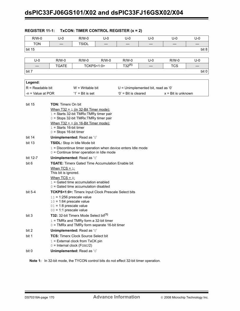
dsPIC33FJ06GS101/X02 and dsPIC33FJ16GSX02/X04
REGISTER 11-1: TxCON: TIMER CONTROL REGISTER (x = 2)
R/W-0 U-0 R/W-0 U-0 U-0 U-0 U-0 U-0TON — TSIDL — — — — —
bit 15 bit 8
U-0 R/W-0 R/W-0 R/W-0 R/W-0 U-0 R/W-0 U-0— TGATE TCKPS<1:0> T32(1) — TCS —
bit 7 bit 0
Legend:R = Readable bit W = Writable bit U = Unimplemented bit, read as ‘0’-n = Value at POR ‘1’ = Bit is set ‘0’ = Bit is cleared x = Bit is unknown
bit 15 TON: Timerx On bitWhen T32 = 1 (in 32-Bit Timer mode):1 = Starts 32-bit TMRx:TMRy timer pair0 = Stops 32-bit TMRx:TMRy timer pairWhen T32 = 0 (in 16-Bit Timer mode):1 = Starts 16-bit timer0 = Stops 16-bit timer
bit 14 Unimplemented: Read as ‘0’bit 13 TSIDL: Stop in Idle Mode bit
1 = Discontinue timer operation when device enters Idle mode0 = Continue timer operation in Idle mode
bit 12-7 Unimplemented: Read as ‘0’bit 6 TGATE: Timerx Gated Time Accumulation Enable bit
When TCS = 1:This bit is ignored.When TCS = 0:1 = Gated time accumulation enabled0 = Gated time accumulation disabled
bit 5-4 TCKPS<1:0>: Timerx Input Clock Prescale Select bits11 = 1:256 prescale value10 = 1:64 prescale value01 = 1:8 prescale value00 = 1:1 prescale value
bit 3 T32: 32-bit Timerx Mode Select bit(1)
1 = TMRx and TMRy form a 32-bit timer0 = TMRx and TMRy form separate 16-bit timer
bit 2 Unimplemented: Read as ‘0’bit 1 TCS: Timerx Clock Source Select bit
1 = External clock from TxCK pin0 = Internal clock (FOSC/2)
bit 0 Unimplemented: Read as ‘0’
Note 1: In 32-bit mode, the TYCON control bits do not effect 32-bit timer operation.
DS70318A-page 170 Advance Information © 2008 Microchip Technology Inc.

dsPIC33FJ06GS101/X02 and dsPIC33FJ16GSX02/X04
REGISTER 11-2: TyCON: TIMER CONTROL REGISTER (y = 3)
R/W-0 U-0 R/W-0 U-0 U-0 U-0 U-0 U-0TON(2) — TSIDL(1) — — — — —
bit 15 bit 8
U-0 R/W-0 R/W-0 R/W-0 U-0 U-0 R/W-0 U-0— TGATE(2) TCKPS<1:0>(2) — — TCS(2) —
bit 7 bit 0
Legend:R = Readable bit W = Writable bit U = Unimplemented bit, read as ‘0’-n = Value at POR ‘1’ = Bit is set ‘0’ = Bit is cleared x = Bit is unknown
bit 15 TON: Timery On bit(2)
1 = Starts 16-bit Timerx0 = Stops 16-bit Timerx
bit 14 Unimplemented: Read as ‘0’bit 13 TSIDL: Stop in Idle Mode bit(1)
1 = Discontinue timer operation when device enters Idle mode0 = Continue timer operation in Idle mode
bit 12-7 Unimplemented: Read as ‘0’bit 6 TGATE: Timerx Gated Time Accumulation Enable bit(2)
When TCS = 1:This bit is ignored.When TCS = 0:1 = Gated time accumulation enabled0 = Gated time accumulation disabled
bit 5-4 TCKPS<1:0>: Timerx Input Clock Prescale Select bits(2)
11 = 1:256 prescale value10 = 1:64 prescale value01 = 1:8 prescale value00 = 1:1 prescale value
bit 3-2 Unimplemented: Read as ‘0’bit 1 TCS: Timerx Clock Source Select bit(2)
1 = External clock from TxCK pin0 = Internal clock (FOSC/2)
bit 0 Unimplemented: Read as ‘0’
Note 1: When 32-bit timer operation is enabled (T32 = 1) in the Timer Control (TxCON<3>) register, the TSIDL bitmust be cleared to operate the 32-bit timer in Idle mode.
2: When the 32-bit timer operation is enabled (T32 = 1) in the Timer Control (TxCON<3>) register, these bitshave no effect.
© 2008 Microchip Technology Inc. Advance Information DS70318A-page 171

dsPIC33FJ06GS101/X02 and dsPIC33FJ16GSX02/X04
NOTES:
DS70318A-page 172 Advance Information © 2008 Microchip Technology Inc.

dsPIC33FJ06GS101/X02 and dsPIC33FJ16GSX02/X04
12.0 INPUT CAPTURE
The input capture module is useful in applicationsrequiring frequency (period) and pulse measurement.The dsPIC33FJ06GSX02 and dsPIC33FJ06GSX04devices support up to two input capture channels.
The input capture module captures the 16-bit value ofthe selected Time Base register when an event occursat the ICx pin. The events that cause a capture eventare listed below in three categories:
• Simple Capture Event modes:- Capture timer value on every falling edge of
input at ICx pin- Capture timer value on every rising edge of
input at ICx pin• Capture timer value on every edge (rising and
falling)• Prescaler Capture Event modes:
- Capture timer value on every 4th rising edge of input at ICx pin
- Capture timer value on every 16th rising edge of input at ICx pin
Each input capture channel can select one of thetwo 16-bit timers (Timer2 or Timer3) for the timebase. The selected timer can use either an internalor external clock.
Other operational features include:
• Device wake-up from capture pin during CPU Sleep and Idle modes
• Interrupt on input capture event• 4-word FIFO buffer for capture values
- Interrupt optionally generated after 1, 2, 3 or 4 buffer locations are filled
• Use of input capture to provide additional sources of external interrupts
FIGURE 12-1: INPUT CAPTURE BLOCK DIAGRAM
Note: This data sheet summarizes the featuresof the dsPIC33FJ06GS101/X02 anddsPIC33FJ16GSX02/X04 families ofdevices. It is not intended to be acomprehensive reference source. Tocomplement the information in this datasheet, refer to the dsPIC33F FamilyReference Manual, “Section 12. InputCapture” (DS70198), which is availableon the Microchip website(www.microchip.com).
ICxBUF
ICx PinICM<2:0> (ICxCON<2:0>)
Mode Select3
1 0
Set Flag ICxIF(in IFSn Register)
TMR2 TMR3
Edge Detection Logic
16 16
FIFOR/WLogic
ICxI<1:0>
ICOV, ICBNE (ICxCON<4:3>)
ICxCONInterrupt
Logic
System Bus
From 16-bit Timers
ICTMR(ICxCON<7>)
FIFO
PrescalerCounter(1, 4, 16)
andClock Synchronizer
Note 1: An ‘x’ in a signal, register or bit name denotes the number of the capture channel.
© 2008 Microchip Technology Inc. Advance Information DS70318A-page 173

dsPIC33FJ06GS101/X02 and dsPIC33FJ16GSX02/X04
12.1 Input Capture Registers REGISTER 12-1: ICxCON: INPUT CAPTURE x CONTROL REGISTER (x = 1, 2)
U-0 U-0 R/W-0 U-0 U-0 U-0 U-0 U-0— — ICSIDL — — — — —
bit 15 bit 8
R/W-0 R/W-0 R/W-0 R-0, HC R-0, HC R/W-0 R/W-0 R/W-0ICTMR ICI<1:0> ICOV ICBNE ICM<2:0>
bit 7 bit 0
Legend: HC = Cleared in HardwareR = Readable bit W = Writable bit U = Unimplemented bit, read as ‘0’-n = Value at POR ‘1’ = Bit is set ‘0’ = Bit is cleared x = Bit is unknown
bit 15-14 Unimplemented: Read as ‘0’bit 13 ICSIDL: Input Capture Module Stop in Idle Control bit
1 = Input capture module halts in CPU Idle mode0 = Input capture module continues to operate in CPU Idle mode
bit 12-8 Unimplemented: Read as ‘0’bit 7 ICTMR: Input Capture Timer Select bits
1 = TMR2 contents are captured on capture event0 = TMR3 contents are captured on capture event
bit 6-5 ICI<1:0>: Select Number of Captures per Interrupt bits11 = Interrupt on every fourth capture event10 = Interrupt on every third capture event01 = Interrupt on every second capture event00 = Interrupt on every capture event
bit 4 ICOV: Input Capture Overflow Status Flag bit (read-only)1 = Input capture overflow occurred0 = No input capture overflow occurred
bit 3 ICBNE: Input Capture Buffer Empty Status bit (read-only)1 = Input capture buffer is not empty, at least one more capture value can be read0 = Input capture buffer is empty
bit 2-0 ICM<2:0>: Input Capture Mode Select bits111 = Input capture functions as interrupt pin only when device is in Sleep or Idle mode
Rising edge detect-only, all other control bits are not applicable.110 = Unused (module disabled)101 = Capture mode, every 16th rising edge100 = Capture mode, every 4th rising edge011 = Capture mode, every rising edge010 = Capture mode, every falling edge001 = Capture mode, every edge (rising and falling)
ICI<1:0> bits do not control interrupt generation for this mode.000 = Input capture module turned off
DS70318A-page 174 Advance Information © 2008 Microchip Technology Inc.

dsPIC33FJ06GS101/X02 and dsPIC33FJ16GSX02/X04
13.0 OUTPUT COMPARE
The Output Compare module can select either Timer2or Timer3 for its time base. The module compares thevalue of the timer with the value of one or two compareregisters depending on the operating mode selected.
The state of the output pin changes when the timervalue matches the compare register value. The OutputCompare module generates either a single outputpulse or a sequence of output pulses, by changing thestate of the output pin on the compare match events.The Output Compare module can also generateinterrupts on compare match events.
The Output Compare module has multiple operatingmodes:
• Active Low One-Shot mode• Active High One-Shot mode• Toggle mode• Delayed One-Shot mode• Continuous Pulse mode• PWM mode without fault protection• PWM mode with fault protection
FIGURE 13-1: OUTPUT COMPARE MODULE BLOCK DIAGRAM
Note: This data sheet summarizes the featuresof the dsPIC33FJ06GS101/X02 anddsPIC33FJ16GSX02/X04 families ofdevices. It is not intended to be acomprehensive reference source. Tocomplement the information in this datasheet, refer to the dsPIC33F FamilyReference Manual, Section 13. “OutputCompare” (DS70209), which is availableon the Microchip website(www.microchip.com).
OCxR
Comparator
OutputLogic
OCM<2:0>
Output Enable
OCx
Set Flag bitOCxIF
OCxRS
Mode Select
3
0 1 OCTSEL 0 1
16 16
OCFA
TMR2 TMR2
QSR
TMR3 TMR3 Rollover Rollover
Note: An ‘x’ in a signal, register or bit name denotes the number of the output compare channels.
© 2008 Microchip Technology Inc. Advance Information DS70318A-page 175

dsPIC33FJ06GS101/X02 and dsPIC33FJ16GSX02/X04
13.1 Output Compare ModesConfigure the Output Compare modes by setting theappropriate Output Compare Mode (OCM<2:0>) bits inthe Output Compare Control (OCxCON<2:0>) register.Table 13-1 lists the different bit settings for the Output
Compare modes. Figure 13-2 illustrates the outputcompare operation for various modes. The userapplication must disable the associated timer whenwriting to the output compare control registers to avoidmalfunctions.
TABLE 13-1: OUTPUT COMPARE MODES
FIGURE 13-2: OUTPUT COMPARE OPERATION
OCM<2:0> Mode OCx Pin Initial State OCx Interrupt Generation
000 Module Disabled Controlled by GPIO register —001 Active Low One-Shot 0 OCx Rising edge 010 Active High One-Shot 1 OCx Falling edge011 Toggle Mode Current output is maintained OCx Rising and Falling edge100 Delayed One-Shot 0 OCx Falling edge101 Continuous Pulse mode 0 OCx Falling edge110 PWM mode without fault
protection0, if OCxR is zero
1, if OCxR is non-zeroNo interrupt
111 PWM mode with fault protection 0, if OCxR is zero1, if OCxR is non-zero
OCFA Falling edge for OC1 to OC4
OCxRS
TMRyOCxR
Timer is reset onperiod match
Continuous Pulse Mode(OCM = 101)
PWM Mode(OCM = 110 or 111)
Active Low One-Shot(OCM = 001)
Active High One-Shot(OCM = 010)
Toggle Mode(OCM = 011)
Delayed One-Shot(OCM = 100)
Output Compare Mode enabled
DS70318A-page 176 Advance Information © 2008 Microchip Technology Inc.

dsPIC33FJ06GS101/X02 and dsPIC33FJ16GSX02/X04
REGISTER 13-1: OCxCON: OUTPUT COMPARE x CONTROL REGISTER (x = 1, 2)
U-0 U-0 R/W-0 U-0 U-0 U-0 U-0 U-0— — OCSIDL — — — — —
bit 15 bit 8
U-0 U-0 U-0 R-0 HC R/W-0 R/W-0 R/W-0 R/W-0— — — OCFLT OCTSEL OCM<2:0>
bit 7 bit 0
Legend: HC = Cleared in Hardware HS = Set in HardwareR = Readable bit W = Writable bit U = Unimplemented bit, read as ‘0’-n = Value at POR ‘1’ = Bit is set ‘0’ = Bit is cleared x = Bit is unknown
bit 15-14 Unimplemented: Read as ‘0’bit 13 OCSIDL: Stop Output Compare in Idle Mode Control bit
1 = Output Compare x halts in CPU Idle mode0 = Output Compare x continues to operate in CPU Idle mode
bit 12-5 Unimplemented: Read as ‘0’bit 4 OCFLT: PWM Fault Condition Status bit
1 = PWM Fault condition has occurred (cleared in hardware only)0 = No PWM Fault condition has occurred(This bit is only used when OCM<2:0> = 111.)
bit 3 OCTSEL: Output Compare Timer Select bit1 = Timer3 is the clock source for Compare x0 = Timer2 is the clock source for Compare x
bit 2-0 OCM<2:0>: Output Compare Mode Select bits111 = PWM mode on OCx, Fault pin enabled110 = PWM mode on OCx, Fault pin disabled101 = Initialize OCx pin low, generate continuous output pulses on OCx pin100 = Initialize OCx pin low, generate single output pulse on OCx pin011 = Compare event toggles OCx pin010 = Initialize OCx pin high, compare event forces OCx pin low001 = Initialize OCx pin low, compare event forces OCx pin high 000 = Output compare channel is disabled
© 2008 Microchip Technology Inc. Advance Information DS70318A-page 177
dsPIC33FJ06GS101/X02 and dsPIC33FJ16GSX02/X04
NOTES:
DS70318A-page 178 Advance Information © 2008 Microchip Technology Inc.

dsPIC33FJ06GS101/X02 and dsPIC33FJ16GSX02/X04
14.0 HIGH-SPEED PWM
The High-Speed PWM module on thedsPIC33FJ06GS101/X02 anddsPIC33FJ16GSX02/X04 devices support a widevariety of PWM modes and output formats. This PWMmodule is ideal for power conversion applications suchas:
• AC/DC converters• DC/DC converters• Power Factor Correction• Uninterruptible Power Supply (UPS)• Inverters• Battery chargers• Digital lighting
14.1 Features OverviewThe High-Speed PWM module incorporates followingfeatures:
• 2-4 PWM generators with 4-8 outputs• Individual time base and duty cycle for each of the
eight PWM outputs• Dead time for rising and falling edges:• Duty cycle resolution of 1.04 ns at 40 MIPS• Dead-time resolution of 1.04 ns at 40 MIPS• Phase shift resolution of 1.04 ns at 40 MIPS• Frequency resolution of 1.04 ns at 40 MIPS• PWM modes supported:
- Standard Edge-Aligned- True Independent Output- Complementary- Center-Aligned- Push-Pull- Multi-Phase- Variable Phase- Fixed Off-Time- Current Reset- Current-Limit
• Independent Fault/Current-Limit inputs for each of the eight PWM outputs
• Output override control• Special Event Trigger• PWM capture feature
• Pre-scalar for input clock• Dual Trigger from PWM TO ADC• PWMxH, PWMxL output pin swapping• PWM4H, PWM4L pins Re-mappable• On-the-Fly PWM Frequency, Duty cycle and
Phase Shift changes• Disabling of Individual PWM generators to reduce
power consumption• Leading-Edge Blanking (LEB) functionality
Figure 14-1 conceptualizes the PWM module in asimplified block diagram. Figure 14-2 illustrates howthe module hardware is partitioned for each PWMoutput pair for the Complementary PWM mode. Eachfunctional unit of the PWM module is discussed insubsequent sections.
The PWM module contains four PWM generators. Themodule has up to eight PWM output pins: PWM1H,PWM1L, PWM2H, PWM2L, PWM3H, PWM3L,PWM4H and PWM4L. For complementary outputs,these eight I/O pins are grouped into H/L pairs.
14.2 Feature DescriptionThe PWM module is designed for applications thatrequire:
• high resolution at high PWM frequencies• the ability to drive standard edge-aligned, center-
aligned complementary mode, and push-pull mode outputs
• the ability to create multi-phase PWM outputs
For center-aligned mode, the duty cycle, period phaseand dead-time resolutions will be 8 ns.
Two common, medium-power converter topologies arePush-Pull and Half-Bridge. These designs require thePWM output signal to be switched between alternatepins, as provided by the Push-Pull PWM mode.
Phase shifted PWM describes the situation where eachPWM generator provides outputs, but the phaserelationship between the generator outputs isspecifiable and changeable.
Multi-Phase PWM is often used to improve DC-DCconverter load transient response, and reduce the sizeof output filter capacitors and inductors. MultipleDC/DC converters are often operated in parallel butphase shifted in time. A single PWM output operatingat 250 kHz has a period of 4 µs. But an array of fourPWM channels, staggered by 1 µs each, yields aneffective switching frequency of 1 MHz. Multi-phasePWM applications typically use a fixed-phaserelationship.
Note: This data sheet summarizes the featuresof the dsPIC33FJ06GS101/X02 anddsPIC33FJ16GSX02/X04 families ofdevices. It is not intended to be acomprehensive reference source. Tocomplement the information in this datasheet, refer to the dsPIC33F FamilyReference Manual, “Section 43.High- Speed PWM” (DS70323), which isavailable on the Microchip website(www.microchip.com). Note: Duty cycle, Dead-time, Phase shift and
Frequency resolution is 8.32 ns inCenter-aligned PWM mode.
© 2008 Microchip Technology Inc. Advance Information DS70318A-page 179

dsPIC33FJ06GS101/X02 and dsPIC33FJ16GSX02/X04
Variable Phase PWM is useful in Zero VoltageTransition (ZVT) power converters. Here the PWM dutycycle is always 50%, and the power flow is controlledby varying the relative phase shift between the twoPWM generators.
DS70318A-page 180 Advance Information © 2008 Microchip Technology Inc.
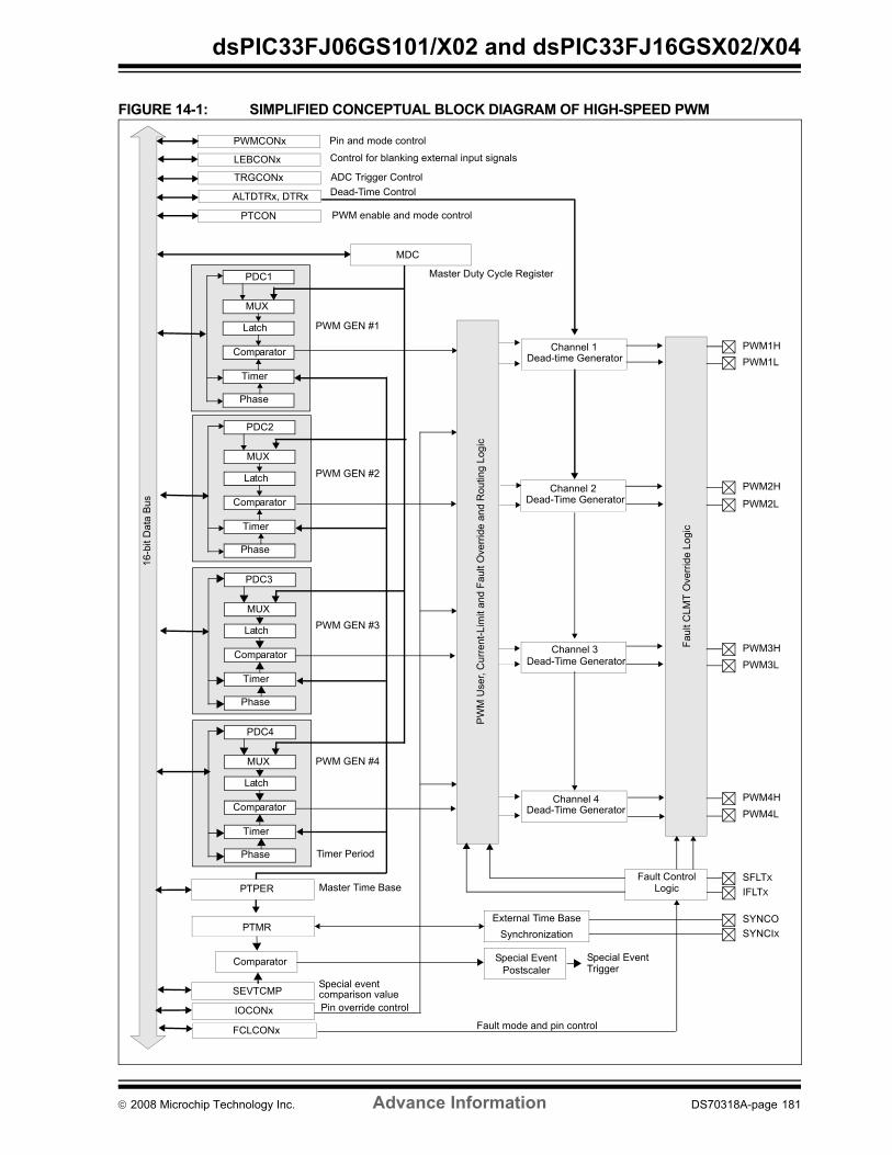
dsPIC33FJ06GS101/X02 and dsPIC33FJ16GSX02/X04
FIGURE 14-1: SIMPLIFIED CONCEPTUAL BLOCK DIAGRAM OF HIGH-SPEED PWM
MUX
Latch
Comparator
Timer
PDC2
Phase
MUX
Latch
Comparator
Timer
PDC3
Phase
MUX
Latch
Comparator
Timer
PDC4
Phase
MUX
Latch
Comparator
Timer
PDC1
PWMCONx
LEBCONx
Channel 1 Dead-time Generator
PTCON
SEVTCMP
Comparator Special Event
IOCONx
PWM enable and mode control
Channel 3 Dead-Time Generator
Channel 4 Dead-Time Generator
ALTDTRx, DTRx Dead-Time Control
Special EventPostscaler
SFLTX
PWM3LPWM3H
PWM2L
PWM2H
16-b
it D
ata
Bus
PWM1LPWM1H
FCLCONx
Pin and mode control
MDC
ADC Trigger Control
Master Duty Cycle Register
Fault mode and pin control
Pin override control
Special event
PTPER
Timer Period
PWM GEN #1
PWM GEN #2
PWM GEN #4
PTMR
Master Time Base
Phase
PWM GEN #3
Channel 2 Dead-Time Generator
PWM4LPWM4H
PW
M U
ser,
Cur
rent
-Lim
it an
d Fa
ult O
verr
ide
and
Rou
ting
Logi
c
Faul
t CLM
T O
verr
ide
Logi
c
Trigger
comparison value
IFLTX
Fault Control Logic
TRGCONx
Control for blanking external input signals
External Time Base Synchronization
SYNCOSYNCIX
© 2008 Microchip Technology Inc. Advance Information DS70318A-page 181
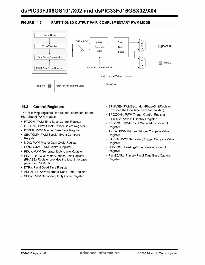
dsPIC33FJ06GS101/X02 and dsPIC33FJ16GSX02/X04
FIGURE 14-2: PARTITIONED OUTPUT PAIR, COMPLEMENTARY PWM MODE
14.3 Control RegistersThe following registers control the operation of theHigh-Speed PWM module.
• PTCON: PWM Time Base Control Register• PTCON2: PWM Clock Divider Select Register• PTPER: PWM Master Time Base Register• SEVTCMP: PWM Special Event Compare
Register• MDC: PWM Master Duty Cycle Register• PWMCONx: PWM Control Register• PDCx: PWM Generator Duty Cycle Register• PHASEx: PWM Primary Phase Shift Register
(PHASEx Register provides the local time base period for PWMxH)
• DTRx: PWM Dead Time Register• ALTDTRx: PWM Alternate Dead Time Register• SDCx: PWM Secondary Duty Cycle Register
• SPHASEx: PWM Secondary Phase Shift Register (Provides the local time base for PWMxL)
• TRGCONx: PWM Trigger Control Register• IOCONx: PWM I/O Control Register• FCLCONx: PWM Fault Current-Limit Control
Register• TRIGx: PWM Primary Trigger Compare Value
Register• STRIGx: PWM Secondary Trigger Compare Value
Register• LEBCONx: Leading-Edge Blanking Control
Register• PWMCAPx: Primary PWM Time Base Capture
Register
PWM Duty Cycle Register
Duty Cycle Comparator
Fault Override Values
Channel override values
Fault Pin Assignment LogicFault Pin
PWMXH
PWMXL
TMR < PDC PWM
Override Logic
Dead
Time
Logic
Fault Active
Phase Offset
MUX
MUX
Timer/Counter
DS70318A-page 182 Advance Information © 2008 Microchip Technology Inc.
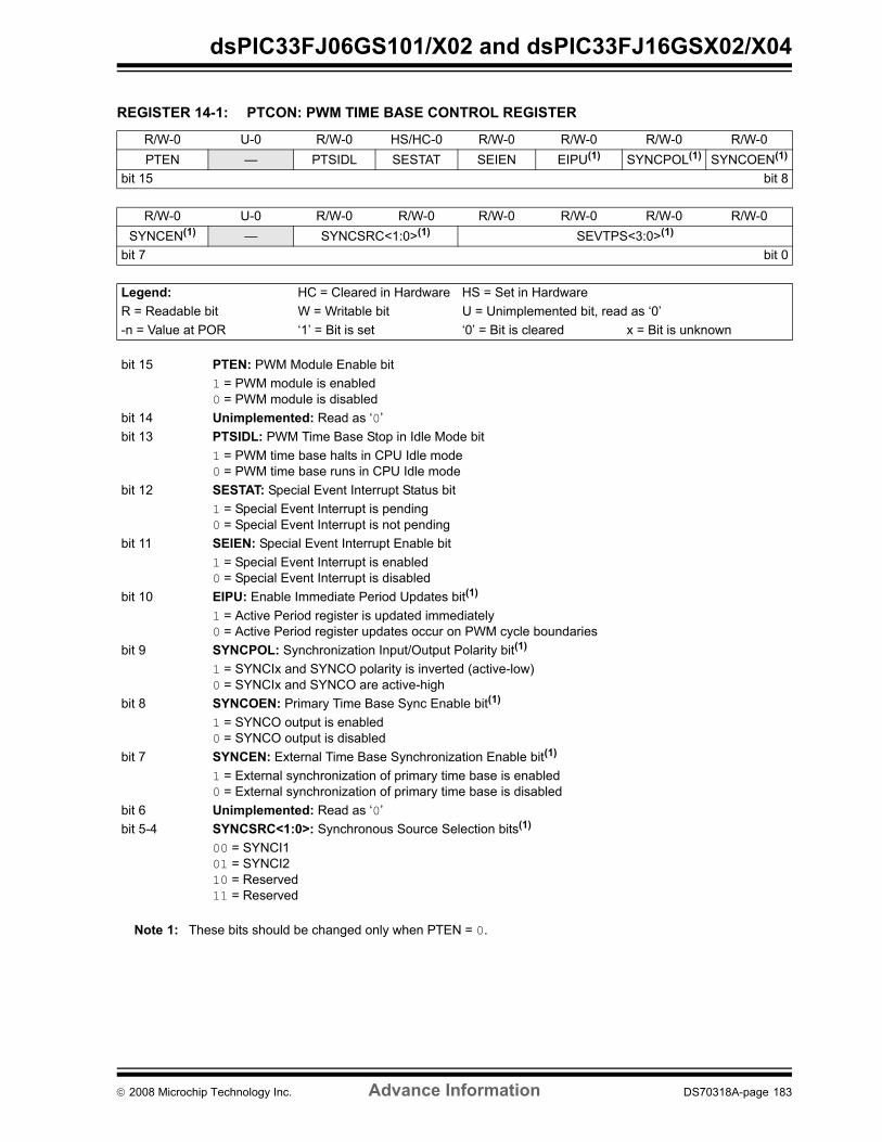
dsPIC33FJ06GS101/X02 and dsPIC33FJ16GSX02/X04
REGISTER 14-1: PTCON: PWM TIME BASE CONTROL REGISTER
R/W-0 U-0 R/W-0 HS/HC-0 R/W-0 R/W-0 R/W-0 R/W-0PTEN — PTSIDL SESTAT SEIEN EIPU(1) SYNCPOL(1) SYNCOEN(1)
bit 15 bit 8
R/W-0 U-0 R/W-0 R/W-0 R/W-0 R/W-0 R/W-0 R/W-0SYNCEN(1) — SYNCSRC<1:0>(1) SEVTPS<3:0>(1)
bit 7 bit 0
Legend: HC = Cleared in Hardware HS = Set in HardwareR = Readable bit W = Writable bit U = Unimplemented bit, read as ‘0’-n = Value at POR ‘1’ = Bit is set ‘0’ = Bit is cleared x = Bit is unknown
bit 15 PTEN: PWM Module Enable bit 1 = PWM module is enabled0 = PWM module is disabled
bit 14 Unimplemented: Read as ‘0’ bit 13 PTSIDL: PWM Time Base Stop in Idle Mode bit
1 = PWM time base halts in CPU Idle mode0 = PWM time base runs in CPU Idle mode
bit 12 SESTAT: Special Event Interrupt Status bit1 = Special Event Interrupt is pending0 = Special Event Interrupt is not pending
bit 11 SEIEN: Special Event Interrupt Enable bit1 = Special Event Interrupt is enabled0 = Special Event Interrupt is disabled
bit 10 EIPU: Enable Immediate Period Updates bit(1)
1 = Active Period register is updated immediately0 = Active Period register updates occur on PWM cycle boundaries
bit 9 SYNCPOL: Synchronization Input/Output Polarity bit(1)
1 = SYNCIx and SYNCO polarity is inverted (active-low)0 = SYNCIx and SYNCO are active-high
bit 8 SYNCOEN: Primary Time Base Sync Enable bit(1)
1 = SYNCO output is enabled0 = SYNCO output is disabled
bit 7 SYNCEN: External Time Base Synchronization Enable bit(1)
1 = External synchronization of primary time base is enabled0 = External synchronization of primary time base is disabled
bit 6 Unimplemented: Read as ‘0’bit 5-4 SYNCSRC<1:0>: Synchronous Source Selection bits(1)
00 = SYNCI101 = SYNCI210 = Reserved11 = Reserved
Note 1: These bits should be changed only when PTEN = 0.
© 2008 Microchip Technology Inc. Advance Information DS70318A-page 183
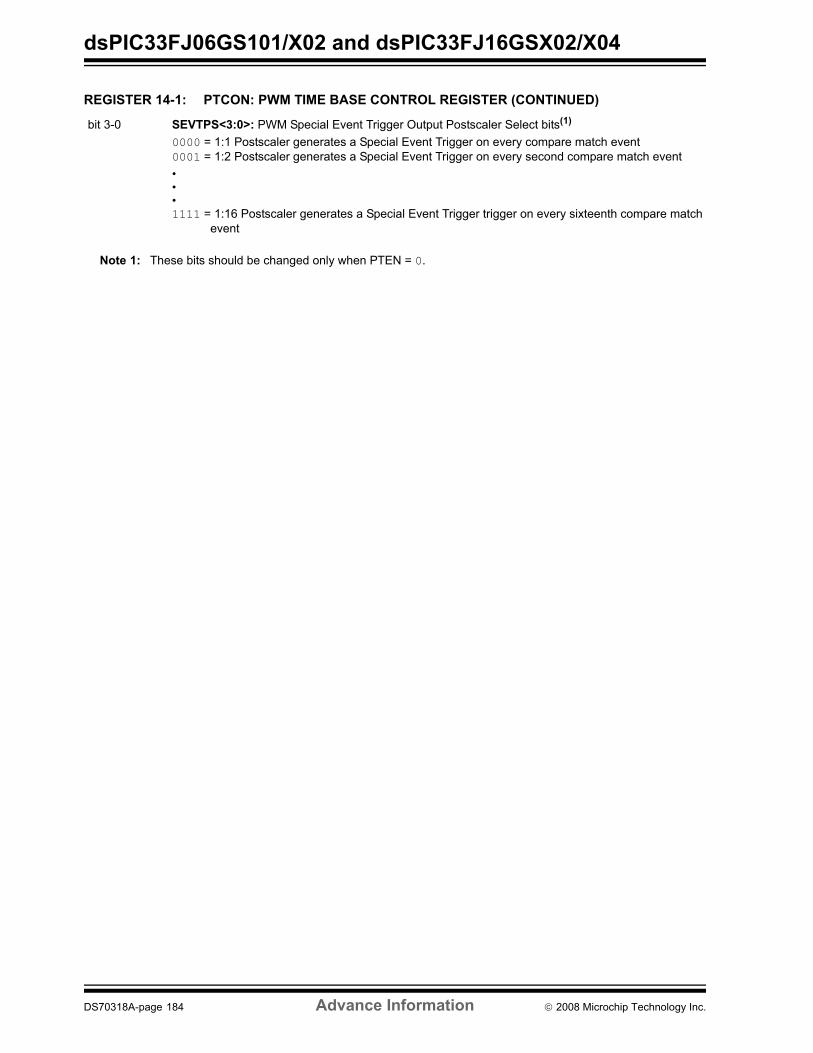
dsPIC33FJ06GS101/X02 and dsPIC33FJ16GSX02/X04
bit 3-0 SEVTPS<3:0>: PWM Special Event Trigger Output Postscaler Select bits(1)
0000 = 1:1 Postscaler generates a Special Event Trigger on every compare match event0001 = 1:2 Postscaler generates a Special Event Trigger on every second compare match event•••1111 = 1:16 Postscaler generates a Special Event Trigger trigger on every sixteenth compare match
event
REGISTER 14-1: PTCON: PWM TIME BASE CONTROL REGISTER (CONTINUED)
Note 1: These bits should be changed only when PTEN = 0.
DS70318A-page 184 Advance Information © 2008 Microchip Technology Inc.

dsPIC33FJ06GS101/X02 and dsPIC33FJ16GSX02/X04
REGISTER 14-2: PTCON2: PWM CLOCK DIVIDER SELECT REGISTER
U-0 U-0 U-0 U-0 U-0 U-0 U-0 U-0— — — — — — — —
bit 15 bit 8
U-0 U-0 U-0 U-0 U-0 R/W-0 R/W-0 R/W-0— — — — — PCLKDIV<2:0>(1)
bit 7 bit 0
Legend:R = Readable bit W = Writable bit U = Unimplemented bit, read as ‘0’-n = Value at POR ‘1’ = Bit is set ‘0’ = Bit is cleared x = Bit is unknown
bit 15-3 Unimplemented: Read as ‘0’bit 2-0 PCLKDIV<2:0>: PWM Input Clock Prescaler (Divider) Select bits(1)
000 = Divide by 1, maximum PWM timing resolution (power-on default)001 = Divide by 2, maximum PWM timing resolution010 = Divide by 4, maximum PWM timing resolution011 = Divide by 8, maximum PWM timing resolution100 = Divide by 16, maximum PWM timing resolution101 = Divide by 32, maximum PWM timing resolution110 = Divide by 64, maximum PWM timing resolution111 = Reserved
Note 1: These bits should be changed only when PTEN = 0. Changing the clock selection during operation willyield unpredictable results.
REGISTER 14-3: PTPER: PWM MASTER TIME BASE REGISTER
R/W-1 R/W-1 R/W-1 R/W-1 R/W-1 R/W-1 R/W-1 R/W-1PTPER <15:8>
bit 15 bit 8
R/W-1 R/W-1 R/W-1 R/W-1 R/W-1 R/W-0 R/W-0 R/W-0PTPER <7:0>
bit 7 bit 0
Legend:R = Readable bit W = Writable bit U = Unimplemented bit, read as ‘0’-n = Value at POR ‘1’ = Bit is set ‘0’ = Bit is cleared x = Bit is unknown
bit 15-0 PTPER<15:0>: PWM Master Time Base (PMTMR) Period Value bits
Note: The minimum value that can be loaded into the PTPER register is 0x0010 and the maximum value is0xFFF8.
© 2008 Microchip Technology Inc. Advance Information DS70318A-page 185
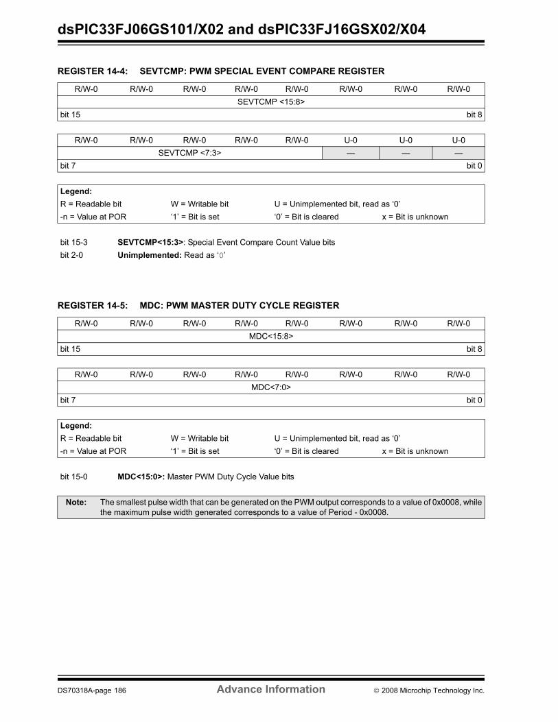
dsPIC33FJ06GS101/X02 and dsPIC33FJ16GSX02/X04
REGISTER 14-4: SEVTCMP: PWM SPECIAL EVENT COMPARE REGISTER
R/W-0 R/W-0 R/W-0 R/W-0 R/W-0 R/W-0 R/W-0 R/W-0SEVTCMP <15:8>
bit 15 bit 8
R/W-0 R/W-0 R/W-0 R/W-0 R/W-0 U-0 U-0 U-0SEVTCMP <7:3> — — —
bit 7 bit 0
Legend:R = Readable bit W = Writable bit U = Unimplemented bit, read as ‘0’-n = Value at POR ‘1’ = Bit is set ‘0’ = Bit is cleared x = Bit is unknown
bit 15-3 SEVTCMP<15:3>: Special Event Compare Count Value bitsbit 2-0 Unimplemented: Read as ‘0’
REGISTER 14-5: MDC: PWM MASTER DUTY CYCLE REGISTER
R/W-0 R/W-0 R/W-0 R/W-0 R/W-0 R/W-0 R/W-0 R/W-0MDC<15:8>
bit 15 bit 8
R/W-0 R/W-0 R/W-0 R/W-0 R/W-0 R/W-0 R/W-0 R/W-0MDC<7:0>
bit 7 bit 0
Legend:R = Readable bit W = Writable bit U = Unimplemented bit, read as ‘0’-n = Value at POR ‘1’ = Bit is set ‘0’ = Bit is cleared x = Bit is unknown
bit 15-0 MDC<15:0>: Master PWM Duty Cycle Value bits
Note: The smallest pulse width that can be generated on the PWM output corresponds to a value of 0x0008, whilethe maximum pulse width generated corresponds to a value of Period - 0x0008.
DS70318A-page 186 Advance Information © 2008 Microchip Technology Inc.

dsPIC33FJ06GS101/X02 and dsPIC33FJ16GSX02/X04
REGISTER 14-6: PWMCONx: PWM CONTROL REGISTER
HS/HC-0 HS/HC-0 HS/HC-0 R/W-0 R/W-0 R/W-0 R/W-0 R/W-0FLTSTAT(1) CLSTAT(1) TRGSTAT FLTIEN CLIEN TRGIEN ITB(3) MDCS(3)
bit 15 bit 8
R/W-0 R/W-0 U-0 U-0 U-0 R/W-0 R/W-0 R/W-0DTC<1:0> — — — CAM(2,3) XPRES IUE
bit 7 bit 0
Legend: HC = Cleared in Hardware HS = Set in HardwareR = Readable bit W = Writable bit U = Unimplemented bit, read as ‘0’-n = Value at POR ‘1’ = Bit is set ‘0’ = Bit is cleared x = Bit is unknown
bit 15 FLTSTAT: Fault Interrupt Status(1)
1 = Fault Interrupt is pending0 = No Fault Interrupt is pendingThis bit is cleared by setting FLTIEN = 0.
bit 14 CLSTAT: Current-Limit Interrupt Status bit(1)
1 = Current-limit interrupt is pending0 = No current-limit interrupt is pendingThis bit is cleared by setting CLIEN = 0.
bit 13 TRGSTAT: Trigger Interrupt Status bit1 = Trigger interrupt is pending0 = No trigger interrupt is pendingThis bit is cleared by setting TRGIEN = 0.
bit 12 FLTIEN: Fault Interrupt Enable bit1 = Fault interrupt is enabled0 = Fault interrupt is disabled and FLTSTAT bit is cleared
bit 11 CLIEN: Current-Limit Interrupt Enable bit1 = Current-limit interrupt enabled0 = Current-limit interrupt disabled and CLSTAT bit is cleared
bit 10 TRGIEN: Trigger Interrupt Enable bit1 = A trigger event generates an interrupt request0 = Trigger event interrupts are disabled and TRGSTAT bit is cleared
bit 9 ITB: Independent Time Base Mode bit(3)
1 = PHASEx/SPHASEx register provides time base period for this PWM generator0 = PTPER register provides timing for this PWM generator
bit 8 MDCS: Master Duty Cycle Register Select bit(3)
1 = MDC register provides duty cycle information for this PWM generator0 = PDCx/SDCx register provides duty cycle information for this PWM generator
bit 7-6 DTC<1:0>: Dead-Time Control bits00 = Positive dead time actively applied for all output modes01 = Negative dead time actively applied for all output modes10 = Dead-time function is disabled11 = Reserved
Note 1: Software must clear the interrupt status here, and the corresponding IFS bit in Interrupt Controller. 2: The Independent Time Base mode (ITB = 1) must be enabled to use Center-Aligned mode. If ITB = 0, the
CAM bit is ignored.3: These bits should be changed only when PTEN = 0. Changing the clock selection during operation will
yield unpredictable results.
© 2008 Microchip Technology Inc. Advance Information DS70318A-page 187

dsPIC33FJ06GS101/X02 and dsPIC33FJ16GSX02/X04
bit 5-3 Unimplemented: Read as ‘0’bit 2 CAM: Center-Aligned Mode Enable bit(2,3)
1 = Center-aligned mode is enabled0 = Center-aligned mode is disabled
bit 1 XPRES: External PWM Reset Control bit1 = Current-limit source resets time base for this PWM generator if it is in independent time base mode 0 = External pins do not affect PWM time base
bit 0 IUE: Immediate Update Enable bit1 = Updates to the active MDC/PDCx/SDCx registers are immediate0 = Updates to the active MDC/PDCx/SDCx registers are synchronized to the PWM time base
REGISTER 14-6: PWMCONx: PWM CONTROL REGISTER (CONTINUED)
Note 1: Software must clear the interrupt status here, and the corresponding IFS bit in Interrupt Controller. 2: The Independent Time Base mode (ITB = 1) must be enabled to use Center-Aligned mode. If ITB = 0, the
CAM bit is ignored.3: These bits should be changed only when PTEN = 0. Changing the clock selection during operation will
yield unpredictable results.
DS70318A-page 188 Advance Information © 2008 Microchip Technology Inc.

dsPIC33FJ06GS101/X02 and dsPIC33FJ16GSX02/X04
REGISTER 14-7: PDCx: PWM GENERATOR DUTY CYCLE REGISTER
R/W-0 R/W-0 R/W-0 R/W-0 R/W-0 R/W-0 R/W-0 R/W-0PDCx<15:8>
bit 15 bit 8
R/W-0 R/W-0 R/W-0 R/W-0 R/W-0 R/W-0 R/W-0 R/W-0PDCx<7:0>
bit 7 bit 0
Legend:R = Readable bit W = Writable bit U = Unimplemented bit, read as ‘0’-n = Value at POR ‘1’ = Bit is set ‘0’ = Bit is cleared x = Bit is unknown
bit 15-0 PDCx<15:0>: PWM Generator # Duty Cycle Value bits
Note: In Independent PWM mode, the PDCx register controls the PWMxH duty cycle only. In Complementary,Redundant, and Push-Pull PWM modes, the PDCx register controls the duty cycle of both the PWMxH andPWMxL. The smallest pulse width that can be generated on the PWM output corresponds to a value of0x0008, while the maximum pulse width generated corresponds to a value of 0xFFEF.
REGISTER 14-8: SDCx: PWM SECONDARY DUTY CYCLE REGISTER
R/W-0 R/W-0 R/W-0 R/W-0 R/W-0 R/W-0 R/W-0 R/W-0SDCx<15:8>
bit 15 bit 8
R/W-0 R/W-0 R/W-0 R/W-0 R/W-0 R/W-0 R/W-0 R/W-0SDCx<7:0>
bit 7 bit 0
Legend:R = Readable bit W = Writable bit U = Unimplemented bit, read as ‘0’-n = Value at POR ‘1’ = Bit is set ‘0’ = Bit is cleared x = Bit is unknown
bit 15-0 SDCx<15:0>: Secondary Duty Cycle for PWMxL output pin
Note: The SDCx register is used in Independent PWM mode only. When used in Independent PWM mode, theSDCx register controls the PWMxL duty cycle. The smallest pulse width that can be generated on the PWMoutput corresponds to a value of 0x0008, while the maximum pulse width generated corresponds to a valueof 0xFFEF.
© 2008 Microchip Technology Inc. Advance Information DS70318A-page 189

dsPIC33FJ06GS101/X02 and dsPIC33FJ16GSX02/X04
REGISTER 14-9: PHASEx: PWM PRIMARY PHASE SHIFT REGISTER
R/W-0 R/W-0 R/W-0 R/W-0 R/W-0 R/W-0 R/W-0 R/W-0PHASEx<15:8>
bit 15 bit 8
R/W-0 R/W-0 R/W-0 R/W-0 R/W-0 R/W-0 R/W-0 R/W-0PHASEx<7:0>
bit 7 bit 0
Legend:R = Readable bit W = Writable bit U = Unimplemented bit, read as ‘0’-n = Value at POR ‘1’ = Bit is set ‘0’ = Bit is cleared x = Bit is unknown
bit 15-0 PHASEx<15:0>: PWM Phase Shift Value or Independent Time Base Period for this PWM Generator bits
Note: If PWMCONx<ITB> = 0, the following applies based on the mode of operation:
• Complementary, Redundant, and Push-Pull Output mode (ICOCONx<PMOD> = 00, 01, or 10)PHASEx<15:0> = Phase shift value for PWMxH and PWMxL outputs
• True Independent Output mode (IOCONx<PMOD> = 11)PHASEx<15:0> = Phase shift value for PWMxH only
If PWMCONx<ITB> = 1, the following applies based on the mode of operation:
• Complementary, Redundant, and Push-Pull Output mode (ICOCONx<PMOD> = 00, 01, or 10)PHASEx<15:0> = Independent time base period value for PWMxH and PWMxL
• True Independent Output mode (IOCONx<PMOD> = 11)PHASEx<15:0> = Independent time base period value for PWMxH only
DS70318A-page 190 Advance Information © 2008 Microchip Technology Inc.
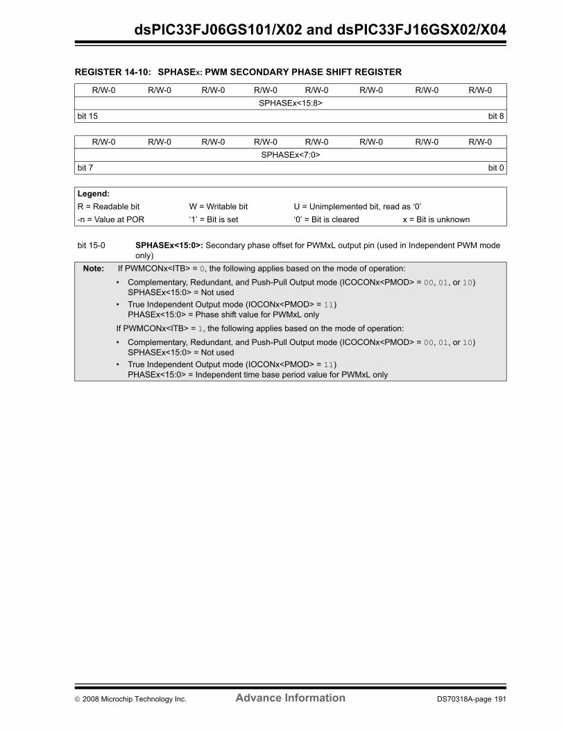
dsPIC33FJ06GS101/X02 and dsPIC33FJ16GSX02/X04
REGISTER 14-10: SPHASEx: PWM SECONDARY PHASE SHIFT REGISTER
R/W-0 R/W-0 R/W-0 R/W-0 R/W-0 R/W-0 R/W-0 R/W-0SPHASEx<15:8>
bit 15 bit 8
R/W-0 R/W-0 R/W-0 R/W-0 R/W-0 R/W-0 R/W-0 R/W-0SPHASEx<7:0>
bit 7 bit 0
Legend:R = Readable bit W = Writable bit U = Unimplemented bit, read as ‘0’-n = Value at POR ‘1’ = Bit is set ‘0’ = Bit is cleared x = Bit is unknown
bit 15-0 SPHASEx<15:0>: Secondary phase offset for PWMxL output pin (used in Independent PWM mode only)
Note: If PWMCONx<ITB> = 0, the following applies based on the mode of operation:
• Complementary, Redundant, and Push-Pull Output mode (ICOCONx<PMOD> = 00, 01, or 10)SPHASEx<15:0> = Not used
• True Independent Output mode (IOCONx<PMOD> = 11)PHASEx<15:0> = Phase shift value for PWMxL only
If PWMCONx<ITB> = 1, the following applies based on the mode of operation:
• Complementary, Redundant, and Push-Pull Output mode (ICOCONx<PMOD> = 00, 01, or 10)SPHASEx<15:0> = Not used
• True Independent Output mode (IOCONx<PMOD> = 11)PHASEx<15:0> = Independent time base period value for PWMxL only
© 2008 Microchip Technology Inc. Advance Information DS70318A-page 191

dsPIC33FJ06GS101/X02 and dsPIC33FJ16GSX02/X04
.
REGISTER 14-11: DTRx: PWM DEAD TIME REGISTER
U-0 U-0 R/W-0 R/W-0 R/W-0 R/W-0 R/W-0 R/W-0— — DTRx<13:8>
bit 15 bit 8
R/W-0 R/W-0 R/W-0 R/W-0 R/W-0 R/W-0 R/W-0 R/W-0DTRx<7:0>
bit 7 bit 0
Legend:R = Readable bit W = Writable bit U = Unimplemented bit, read as ‘0’-n = Value at POR ‘1’ = Bit is set ‘0’ = Bit is cleared x = Bit is unknown
bit 15-14 Unimplemented: Read as ‘0’bit 13-0 DTRx<13:0>: Unsigned 14-bit Dead-Time Value bits for PWMx Dead-Time Unit bits
REGISTER 14-12: ALTDTRx: PWM ALTERNATE DEAD TIME REGISTER U-0 U-0 R/W-0 R/W-0 R/W-0 R/W-0 R/W-0 R/W-0— — ALTDTRx<13:8>
bit 15 bit 8
R/W-0 R/W-0 R/W-0 R/W-0 R/W-0 R/W-0 R/W-0 R/W-0ALTDTR <7:0>
bit 7 bit 0
Legend:R = Readable bit W = Writable bit U = Unimplemented bit, read as ‘0’-n = Value at POR ‘1’ = Bit is set ‘0’ = Bit is cleared x = Bit is unknown
bit 15-14 Unimplemented: Read as ‘0’bit 13-0 ALTDTRx<13:0>: Unsigned 14-bit Dead-Time Value bits for PWMx Dead-Time Unit bits
DS70318A-page 192 Advance Information © 2008 Microchip Technology Inc.

dsPIC33FJ06GS101/X02 and dsPIC33FJ16GSX02/X04
REGISTER 14-13: TRGCONx: PWM TRIGGER CONTROL REGISTER
R/W-0 R/W-0 R/W-0 R/W-0 U-0 U-0 U-0 U-0TRGDIV<3:0> — — — —
bit 15 bit 8
R/W-0 U-0 R/W-0 R/W-0 R/W-0 R/W-0 R/W-0 R/W-0DTM(1) — TRGSTRT<5:0>
bit 7 bit 0
Legend:R = Readable bit W = Writable bit U = Unimplemented bit, read as ‘0’-n = Value at POR ‘1’ = Bit is set ‘0’ = Bit is cleared x = Bit is unknown
bit 15-12 TRGDIV<3:0>: Trigger # Output Divider0000 = Trigger output for every trigger event0001 = Trigger output for every 2nd trigger event0010 = Trigger output for every 3rd trigger event0011 = Trigger output for every 4th trigger event0100 = Trigger output for every 5th trigger event0101 = Trigger output for every 6th trigger event0110 = Trigger output for every 7th trigger event0111 = Trigger output for every 8th trigger event1000 = Trigger output for every 9th trigger event1001 = Trigger output for every 10th trigger event1010 = Trigger output for every 11th trigger event1011 = Trigger output for every 12th trigger event1100 = Trigger output for every 13th trigger event1101 = Trigger output for every 14th trigger event1110 = Trigger output for every 15th trigger event1111 = Trigger output for every 16th trigger event
bit 11-8 Unimplemented: Read as ‘0’bit 7 DTM: Dual Trigger Mode(1)
1 = Secondary Trigger event is combined with the primary trigger event to create PWM trigger.0 = Secondary Trigger event is not combined with the primary trigger event to create PWM trigger. Two
separate PWM triggers are generated.bit 6 Unimplemented: Read as ‘0’bit 5-0 TRGSTRT<5:0>: Trigger Postscaler Start Enable Select bits
000000 = Wait 0 PWM cycles before generating the first trigger event after the module is enabled000001 = Wait 1 PWM cycles before generating the first trigger event after the module is enabled000010 = Wait 1 PWM cycles before generating the first trigger event after the module is enabled•••111111 = Wait 63 PWM cycles before generating the first trigger event after the module is enabled
Note 1: The secondary generator cannot generate PWM trigger interrupts.
© 2008 Microchip Technology Inc. Advance Information DS70318A-page 193

dsPIC33FJ06GS101/X02 and dsPIC33FJ16GSX02/X04
REGISTER 14-14: IOCONx: PWM I/O CONTROL REGISTER
R/W-0 R/W-0 R/W-0 R/W-0 R/W-0 R/W-0 R/W-0 R/W-0PENH PENL POLH POLL PMOD<1:0>(1) OVRENH OVRENL
bit 15 bit 8
R/W-0 R/W-0 R/W-0 R/W-0 R/W-0 R/W-0 R/W-0 R/W-0OVRDAT<1:0> FLTDAT<1:0> CLDAT<1:0> SWAP OSYNC
bit 7 bit 0
Legend:R = Readable bit W = Writable bit U = Unimplemented bit, read as ‘0’-n = Value at POR ‘1’ = Bit is set ‘0’ = Bit is cleared x = Bit is unknown
bit 15 PENH: PWMH Output Pin Ownership bit1 = PWM module controls PWMxH pin0 = GPIO module controls PWMxH pin
bit 14 PENL: PWML Output Pin Ownership bit1 = PWM module controls PWMxL pin0 = GPIO module controls PWMxL pin
bit 13 POLH: PWMH Output Pin Polarity bit1 = PWMxH pin is active-low0 = PWMxH pin is high active
bit 12 POLL: PWML Output Pin Polarity bit1 = PWMxL pin is active-low0 = PWMxL pin is high active
bit 11-10 PMOD<1:0>: PWM # I/O Pin Mode bits(1)
00 = PWM I/O pin pair is in the Complementary Output mode01 = PWM I/O pin pair is in the Redundant Output mode10 = PWM I/O pin pair is in the Push-Pull Output mode11 = PWM I/O pin pair is in the True Independent Output mode
bit 9 OVRENH: Override Enable for PWMxH Pin bit1 = OVRDAT<1> provides data for output on PWMxH pin0 = PWM generator provides data for PWMxH pin
bit 8 OVRENL: Override Enable for PWMxL Pin bit1 = OVRDAT<0> provides data for output on PWMxL pin0 = PWM generator provides data for PWMxL pin
bit 7-6 OVRDAT<1:0>: Data for PWMxH and PWMxL Pins if Override is Enabled bitsIf OVERENH = 1 then OVRDAT<1> provides data for PWMxHIf OVERENL = 1 then OVRDAT<0> provides data for PWMxL
bit 5-4 FLTDAT<1:0>: Data for PWMxH and PWMxL Pins if FLTMOD is Enabled bitsFCLCONx<IFLTMOD> = 0: Normal Fault modeIf Fault active, then FLTDAT<1> provides data for PWMxHIf Fault active, then FLTDAT<0> provides data for PWMxL
FCLCONx<IFLTMOD> = 1: Independent Fault modeIf Current-Limit active, then FLTDAT<1> provides data for PWMxHIf Fault active, then FLTDAT<0> provides data for PWMxL
Note 1: These bits should be changed only when PTEN = 0. Changing the clock selection during operation willyield unpredictable results.
DS70318A-page 194 Advance Information © 2008 Microchip Technology Inc.

dsPIC33FJ06GS101/X02 and dsPIC33FJ16GSX02/X04
bit 3-2 CLDAT<1:0>: Data for PWMxH and PWMxL Pins if CLMODE is Enabled bitsFCLCONx<IFLTMOD> = 0: Normal Fault modeIf current-limit active, then CLDAT<1> provides data for PWMxHIf current-limit active, then CLDAT<0> provides data for PWMxL
FCLCONx<IFLTMOD> = 1: Independent Fault modeCLDAT<1:0> is ignored
bit 1 SWAP<1:0>: SWAP PWMxH and PWMxL pins1 = PWMxH output signal is connected to PWMxL pin and PWMxL signal is connected to PWMxH pins0 = PWMxH and PWMxL pins are mapped to their respective pins
bit 0 OSYNC: Output Override Synchronization bit1 = Output overrides via the OVRDAT<1:0> bits are synchronized to the PWM time base0 = Output overrides via the OVDDAT<1:0> bits occur on next CPU clock boundary
REGISTER 14-14: IOCONx: PWM I/O CONTROL REGISTER (CONTINUED)
Note 1: These bits should be changed only when PTEN = 0. Changing the clock selection during operation willyield unpredictable results.
© 2008 Microchip Technology Inc. Advance Information DS70318A-page 195

dsPIC33FJ06GS101/X02 and dsPIC33FJ16GSX02/X04
REGISTER 14-15: FCLCONx: PWM FAULT CURRENT-LIMIT CONTROL REGISTER
R/W-0 R/W-0 R/W-0 R/W-0 R/W-0 R/W-0 R/W-0 R/W-0IFLTMOD CLSRC<4:0> CLPOL(1) CLMOD
bit 15 bit 8
R/W-0 R/W-0 R/W-0 R/W-0 R/W-0 R/W-0 R/W-0 R/W-0FLTSRC<4:0> FLTPOL(1) FLTMOD<1:0>
bit 7 bit 0
Legend:R = Readable bit W = Writable bit U = Unimplemented bit, read as ‘0’-n = Value at POR ‘1’ = Bit is set ‘0’ = Bit is cleared x = Bit is unknown
bit 15 IFLTMOD: Independent Fault Mode Enable bit1 = Independent fault mode: Current-limit input maps FLTDAT<1> to PWMxH output, and Fault input maps FLTDAT<0> to PWMxL output. The CLDAT<1:0> bits are not used for override functions0 = Normal fault mode: Current-limit feature maps CLDAT<1:0> bits to the PWMxH and PWMxL
outputs. The PWM fault feature maps FLTDAT<1:0> to the PWMxH and PWMxL outputs.bit 14-10 CLSRC<4:0>: Current-Limit control signal source select for PWM # generator
00000 = Analog Comparator 100001 = Analog Comparator 200010 = Analog Comparator 300011 = Analog Comparator 4
00100 = Reserved•••00111 = Reserved
01000 = Fault 101001 = Fault 201010 = Fault 301011 = Fault 401100 = Fault 501101 = Fault 601110 = Fault 701111 = Fault 8
10000 = Reserved•••11111 = Reserved
bit 9 CLPOL: Current-Limit Polarity bit for PWM Generator #(1)
1 = The selected current-limit source is active-low0 = The selected current-limit source is high active
Note 1: These bits should be changed only when PTEN = 0. Changing the clock selection during operation willyield unpredictable results.
DS70318A-page 196 Advance Information © 2008 Microchip Technology Inc.

dsPIC33FJ06GS101/X02 and dsPIC33FJ16GSX02/X04
bit 8 CLMODE: Current-Limit Mode Enable bit for PWM Generator #1 = Current-limit function is enabled0 = Current-limit function is disabled
bit 7-3 FLTSRC<4:0>: Fault Control Signal Source Select for PWM Generator # bits00000 = Analog Comparator 100001 = Analog Comparator 200010 = Analog Comparator 300011 = Analog Comparator 4
00100 = Reserved•••00111 = Reserved
01000 = Fault 101001 = Fault 201010 = Fault 301011 = Fault 401100 = Fault 501101 = Fault 601110 = Fault 701111 = Fault 8
10000 = Reserved•••11111 = Reserved
bit 2 FLTPOL: Fault Polarity bit for PWM Generator #(1)
1 = The selected Fault source is active-low0 = The selected Fault source is high active
bit 1-0 FLTMOD<1:0>: Fault Mode bits for PWM Generator #00 = The selected Fault source forces PWMxH, PWMxL pins to FLTDAT values (latched condition)01 = The selected Fault source forces PWMxH, PWMxL pins to FLTDAT values (cycle)10 = Reserved11 = Fault input is disabled
REGISTER 14-15: FCLCONx: PWM FAULT CURRENT-LIMIT CONTROL REGISTER (CONTINUED)
Note 1: These bits should be changed only when PTEN = 0. Changing the clock selection during operation willyield unpredictable results.
© 2008 Microchip Technology Inc. Advance Information DS70318A-page 197
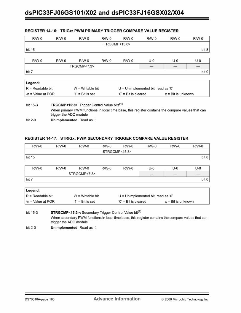
dsPIC33FJ06GS101/X02 and dsPIC33FJ16GSX02/X04
REGISTER 14-16: TRIGx: PWM PRIMARY TRIGGER COMPARE VALUE REGISTER
R/W-0 R/W-0 R/W-0 R/W-0 R/W-0 R/W-0 R/W-0 R/W-0TRGCMP<15:8>
bit 15 bit 8
R/W-0 R/W-0 R/W-0 R/W-0 R/W-0 U-0 U-0 U-0TRGCMP<7:3> — — —
bit 7 bit 0
Legend:R = Readable bit W = Writable bit U = Unimplemented bit, read as ‘0’-n = Value at POR ‘1’ = Bit is set ‘0’ = Bit is cleared x = Bit is unknown
bit 15-3 TRGCMP<15:3>: Trigger Control Value bits(1) When primary PWM functions in local time base, this register contains the compare values that can trigger the ADC module
bit 2-0 Unimplemented: Read as ‘0’
REGISTER 14-17: STRIGx: PWM SECONDARY TRIGGER COMPARE VALUE REGISTER
R/W-0 R/W-0 R/W-0 R/W-0 R/W-0 R/W-0 R/W-0 R/W-0STRGCMP<15:8>
bit 15 bit 8
R/W-0 R/W-0 R/W-0 R/W-0 R/W-0 U-0 U-0 U-0STRGCMP<7:3> — — —
bit 7 bit 0
Legend:R = Readable bit W = Writable bit U = Unimplemented bit, read as ‘0’-n = Value at POR ‘1’ = Bit is set ‘0’ = Bit is cleared x = Bit is unknown
bit 15-3 STRGCMP<15:3>: Secondary Trigger Control Value bit(1) When secondary PWM functions in local time base, this register contains the compare values that can trigger the ADC module
bit 2-0 Unimplemented: Read as ‘0’
DS70318A-page 198 Advance Information © 2008 Microchip Technology Inc.

dsPIC33FJ06GS101/X02 and dsPIC33FJ16GSX02/X04
REGISTER 14-18: LEBCONx: LEADING-EDGE BLANKING CONTROL REGISTER
R/W-0 R/W-0 R/W-0 R/W-0 R/W-0 R/W-0 R/W-0 R/W-0PHR PHF PLR PLF FLTLEBEN CLLEBEN LEB<9:8>
bit 15 bit 8
R/W-0 R/W-0 R/W-0 R/W-0 R/W-0 U-0 U-0 U-0LEB<7:3> — — —
bit 7 bit 0
Legend:R = Readable bit W = Writable bit U = Unimplemented bit, read as ‘0’-n = Value at POR ‘1’ = Bit is set ‘0’ = Bit is cleared x = Bit is unknown
bit 15 PHR: PWMxH Rising Edge Trigger Enable bit1 = Rising edge of PWMxH will trigger LEB counter0 = LEB ignores rising edge of PWMxH
bit 14 PHF: PWMH Falling Edge Trigger Enable bit1 = Falling edge of PWMxH will trigger LEB counter0 = LEB ignores falling edge of PWMxH
bit 13 PLR: PWML Rising Edge Trigger Enable bit1 = Rising edge of PWMxL will trigger LEB counter0 = LEB ignores rising edge of PWMxL
bit 12 PLF: PWML Falling Edge Trigger Enable bit1 = Falling edge of PWMxL will trigger LEB counter0 = LEB ignores falling edge of PWMxL
bit 11 FLTLEBEN: Fault Input LEB Enable bit1 = Leading Edge Blanking is applied to selected Fault Input0 = Leading Edge Blanking is not applied to selected Fault Input
bit 10 CLLEBEN: Current-Limit LEB Enable bit1 = Leading Edge Blanking is applied to selected Current-Limit Input0 = Leading Edge Blanking is not applied to selected Current-Limit Input
bit 9-3 LEB: Leading Edge Blanking for Current-Limit and Fault Inputs bitsValue is 8 nsec increments
bit 2-0 Unimplemented: Read as ‘0’
© 2008 Microchip Technology Inc. Advance Information DS70318A-page 199

dsPIC33FJ06GS101/X02 and dsPIC33FJ16GSX02/X04
REGISTER 14-19: PWMCAPx: PRIMARY PWM TIME BASE CAPTURE REGISTER
R/W-0 R/W-0 R/W-0 R/W-0 R/W-0 R/W-0 R/W-0 R/W-0PWMCAP<15:8>
bit 15 bit 8
R/W-0 R/W-0 R/W-0 R/W-0 R/W-0 U-0 U-0 U-0PWMCAP<7:3> — — —
bit 7 bit 0
Legend:R = Readable bit W = Writable bit U = Unimplemented bit, read as ‘0’-n = Value at POR ‘1’ = Bit is set ‘0’ = Bit is cleared x = Bit is unknown
bit 15-3 PWMCAP<15:3>: Captured PWM Time Base Value(1,2)
The value in this register represents the captured PWM time base value when a leading edge isdetected on the current-limit input.
bit 2-0 Unimplemented: Read as ‘0’
Note 1: The capture feature is only available on primary output (PWMxH).
2: This feature is active only after LEB processing on the current-limit input signal is complete.
DS70318A-page 200 Advance Information © 2008 Microchip Technology Inc.

dsPIC33FJ06GS101/X02 and dsPIC33FJ16GSX02/X04
15.0 SERIAL PERIPHERAL INTERFACE (SPI)
The Serial Peripheral Interface (SPI) module is asynchronous serial interface useful for communicatingwith other peripheral or microcontroller devices. Theseperipheral devices can be serial EEPROMs, shiftregisters, display drivers, analog-to-digital convertersand so on. The SPI module is compatible with SPI andSIOP from Motorola®.
The SPI module consists of a 16-bit shift register,SPIxSR (where x = 1), used for shifting data in and out,and a buffer register, SPIxBUF. A control register,SPIxCON, configures the module. Additionally, a statusregister, SPIxSTAT, indicates status conditions.
The serial interface consists of 4 pins:
• SDIx (serial data input)• SDOx (serial data output)• SCKx (shift clock input or output)• SSx (active low slave select).
In Master mode operation, SCK is a clock output. InSlave mode, it is a clock input.
15.1 InterruptsA series of 8 or 16 clock pulses shift out bits from theSPIxSR to SDOx pin and simultaneously shift in datafrom the SDIx pin. An interrupt is generated when thetransfer is complete and the corresponding interrupt flagbit (SPIxF1IE) is set. This interrupt can be disabledthrough an interrupt enable bit (SPIxF1IE).
15.2 Receive OperationsThe receive operation is double-buffered. When acomplete byte is received, it is transferred from SPIxSRto SPIxBUF.
If the receive buffer is full when new data is beingtransferred from SPIxSR to SPIxBUF, the module setsthe SPIROV bit, indicating an overflow condition. Thetransfer of the data from SPIxSR to SPIxBUF is notcompleted, and the new data is lost. The module will notrespond to SCL transitions while SPIROV is ‘1’,effectively disabling the module until SPIxBUF is read byuser software.
15.3 Transmit OperationsTransmit writes are also double-buffered. The userapplication writes to SPIxBUF. When the Master or Slavetransfer is completed, the contents of the shift register(SPIxSR) are moved to the receive buffer. If any transmitdata has been written to the buffer register, the contentsof the transmit buffer are moved to SPIxSR. The receiveddata is thus placed in SPIxBUF and the transmit data inSPIxSR is ready for the next transfer.
15.4 SPI Setup: Master ModeTo set up the SPI module for the Master mode ofoperation:
1. If using interrupts:a) Clear the SPIxIF bit in the respective IFSn
register.b) Set the SPIxIE bit in the respective IECn
register.c) Write the SPIxIP bits in the respective IPCn
register to set the interrupt priority.2. Write the desired settings to the SPIxCON
register with MSTEN (SPIxCON1<5>) = 1. 3. Clear the SPIROV bit (SPIxSTAT<6>).4. Enable SPI operation by setting the SPIEN bit
(SPIxSTAT<15>).5. Write the data to be transmitted to the SPIxBUF
register. Transmission (and reception) will start assoon as data is written to the SPIxBUF register.
Note: This data sheet summarizes the featuresof the dsPIC33FJ06GS101/X02 anddsPIC33FJ16GSX02/X04 families ofdevices. It is not intended to be acomprehensive reference source. Tocomplement the information in this datasheet, refer to the dsPIC33F FamilyReference Manual, “Section 18. SerialPeripheral Interface (SPI)” (DS70206),which is available on the Microchipwebsite (www.microchip.com).
Note: Both the transmit buffer (SPIxTXB) andthe receive buffer (SPIxRXB) are mappedto the same register address, SPIxBUF.Do not perform read-modify-writeoperations (such as bit-orientedinstructions) on the SPIxBUF register.
© 2008 Microchip Technology Inc. Advance Information DS70318A-page 201

dsPIC33FJ06GS101/X02 and dsPIC33FJ16GSX02/X04
15.5 SPI Setup: Slave ModeTo set up the SPI module for the Slave mode of operation:
1. Clear the SPIxBUF register.2. If using interrupts:
a) Clear the SPIxIF bit in the respective IFSnregister.
b) Set the SPIxIE bit in the respective IECnregister.
c) Write the SPIxIP bits in the respective IPCnregister to set the interrupt priority.
3. Write the desired settings to the SPIxCON1 andSPIxCON2 registers with MSTEN(SPIxCON1<5>) = 0.
4. Clear the SMP bit.5. If the CKE bit is set, then set the SSEN bit
(SPIxCON1<7>) to enable the SSx pin.6. Clear the SPIROV bit (SPIxSTAT<6>).7. Enable SPI operation by setting the SPIEN bit
(SPIxSTAT<15>).
The SPI module generates an interrupt indicatingcompletion of a byte or word transfer, as well as aseparate interrupt for all SPI error conditions.
FIGURE 15-1: SPI MODULE BLOCK DIAGRAM
Internal Data Bus
SDIx
SDOx
SSx
SCKx
SPIxSRbit 0
Shift Control
EdgeSelect
FCYPrimary1:1/4/16/64
Enable
Prescaler
Sync
SPIxBUF
Control
TransferTransfer
Write SPIxBUFRead SPIxBUF
16
SPIxCON1<1:0>
SPIxCON1<4:2>
Master Clock
ClockControl
SecondaryPrescaler
1:1 to 1:8
SPIxRXB SPIxTXB
DS70318A-page 202 Advance Information © 2008 Microchip Technology Inc.

dsPIC33FJ06GS101/X02 and dsPIC33FJ16GSX02/X04
FIGURE 15-2: SPI MASTER/SLAVE CONNECTION
FIGURE 15-3: SPI MASTER, FRAME MASTER CONNECTION DIAGRAM
FIGURE 15-4: SPI MASTER, FRAME SLAVE CONNECTION DIAGRAM
Serial Receive Buffer(SPIxRXB)
LSbMSb
SDIx
SDOx
PROCESSOR 2 (SPI Slave)
SCKx
SSx(1)
Serial Transmit Buffer(SPIxTXB)
Serial Receive Buffer(SPIxRXB)
Shift Register(SPIxSR)
MSb LSb
SDOx
SDIx
PROCESSOR 1 (SPI Master)
Serial Clock
(SSEN (SPIxCON1<7>) = 1 and MSTEN (SPIxCON1<5>) = 0)
Note 1: Using the SSx pin in Slave mode of operation is optional.2: User application must write transmit data to or read received data from SPIxBUF. The SPIxTXB and SPIxRXB registers
are memory mapped to SPIxBUF.
SCKx
Serial Transmit Buffer(SPIxTXB)
(MSTEN (SPIxCON1<5>) = 1)
SPI Buffer(SPIxBUF)(2)
SPI Buffer(SPIxBUF)(2)
Shift Register(SPIxSR)
SSx
SDOx
SDIx
dsPIC33F
Serial Clock
SSx
SCKx
Frame SyncPulse
SDIx
SDOx
PROCESSOR 2
SSx
SCKx
SDOx
SDIx
dsPIC33F
Serial Clock
SSx
SCKx
Frame SyncPulse
SDIx
SDOx
PROCESSOR 2
SSx
SCKx
© 2008 Microchip Technology Inc. Advance Information DS70318A-page 203

dsPIC33FJ06GS101/X02 and dsPIC33FJ16GSX02/X04
FIGURE 15-5: SPI SLAVE, FRAME MASTER CONNECTION DIAGRAM
FIGURE 15-6: SPI SLAVE, FRAME SLAVE CONNECTION DIAGRAM
EQUATION 15-1: RELATIONSHIP BETWEEN DEVICE AND SPI CLOCK SPEED
TABLE 15-1: SAMPLE SCKx FREQUENCIES
FCY = 40 MHzSecondary Prescaler Settings
1:1 2:1 4:1 6:1 8:1
Primary Prescaler Settings 1:1 Invalid Invalid 10000 6666.67 50004:1 10000 5000 2500 1666.67 1250
16:1 2500 1250 625 416.67 312.5064:1 625 312.5 156.25 104.17 78.125
FCY = 5 MHz
Primary Prescaler Settings 1:1 5000 2500 1250 833 6254:1 1250 625 313 208 156
16:1 313 156 78 52 3964:1 78 39 20 13 10
Note: SCKx frequencies shown in kHz.
SDOx
SDIx
dsPIC33F
Serial Clock
SSx
SCKx
Frame SyncPulse
SDIx
SDOx
PROCESSOR 2
SSx
SCKx
SDOx
SDIx
dsPIC33F
Serial Clock
SSx
SCKx
Frame SyncPulse
SDIx
SDOx
PROCESSOR 2
SSx
SCKx
Primary Prescaler * Secondary PrescalerFCY
FSCK =
DS70318A-page 204 Advance Information © 2008 Microchip Technology Inc.

dsPIC33FJ06GS101/X02 and dsPIC33FJ16GSX02/X04
REGISTER 15-1: SPIxSTAT: SPIx STATUS AND CONTROL REGISTER
R/W-0 U-0 R/W-0 U-0 U-0 U-0 U-0 U-0SPIEN — SPISIDL — — — — —
bit 15 bit 8
U-0 R/C-0 U-0 U-0 U-0 U-0 R-0 R-0— SPIROV — — — — SPITBF SPIRBF
bit 7 bit 0
Legend: C = Clearable bitR = Readable bit W = Writable bit U = Unimplemented bit, read as ‘0’-n = Value at POR ‘1’ = Bit is set ‘0’ = Bit is cleared x = Bit is unknown
bit 15 SPIEN: SPIx Enable bit1 = Enables module and configures SCKx, SDOx, SDIx and SSx as serial port pins0 = Disables module
bit 14 Unimplemented: Read as ‘0’bit 13 SPISIDL: Stop in Idle Mode bit
1 = Discontinue module operation when device enters Idle mode0 = Continue module operation in Idle mode
bit 12-7 Unimplemented: Read as ‘0’bit 6 SPIROV: Receive Overflow Flag bit
1 = A new byte/word is completely received and discarded. The user software has not read the previous data in the SPIxBUF register.
0 = No overflow has occurred.bit 5-2 Unimplemented: Read as ‘0’bit 1 SPITBF: SPIx Transmit Buffer Full Status bit
1 = Transmit not yet started, SPIxTXB is full0 = Transmit started, SPIxTXB is emptyAutomatically set in hardware when CPU writes SPIxBUF location, loading SPIxTXBAutomatically cleared in hardware when SPIx module transfers data from SPIxTXB to SPIxSR
bit 0 SPIRBF: SPIx Receive Buffer Full Status bit1 = Receive complete, SPIxRXB is full0 = Receive is not complete, SPIxRXB is emptyAutomatically set in hardware when SPIx transfers data from SPIxSR to SPIxRXBAutomatically cleared in hardware when core reads SPIxBUF location, reading SPIxRXB
© 2008 Microchip Technology Inc. Advance Information DS70318A-page 205
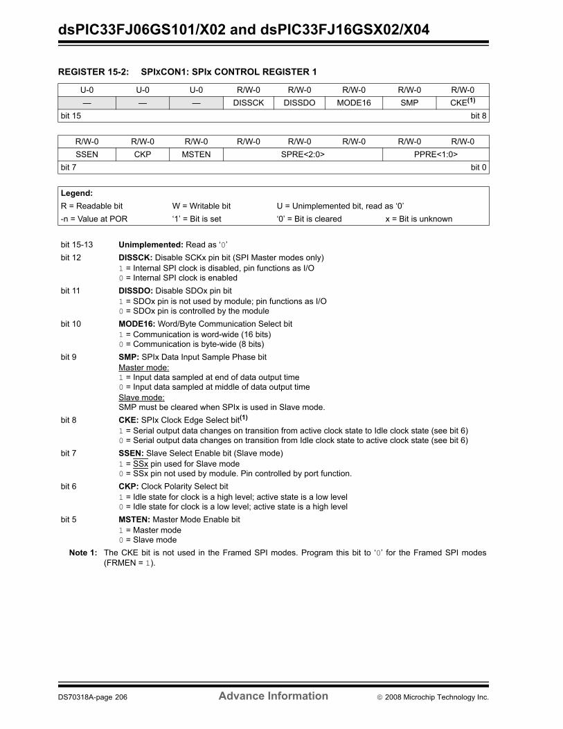
dsPIC33FJ06GS101/X02 and dsPIC33FJ16GSX02/X04
REGISTER 15-2: SPIXCON1: SPIx CONTROL REGISTER 1
U-0 U-0 U-0 R/W-0 R/W-0 R/W-0 R/W-0 R/W-0— — — DISSCK DISSDO MODE16 SMP CKE(1)
bit 15 bit 8
R/W-0 R/W-0 R/W-0 R/W-0 R/W-0 R/W-0 R/W-0 R/W-0SSEN CKP MSTEN SPRE<2:0> PPRE<1:0>
bit 7 bit 0
Legend:R = Readable bit W = Writable bit U = Unimplemented bit, read as ‘0’-n = Value at POR ‘1’ = Bit is set ‘0’ = Bit is cleared x = Bit is unknown
bit 15-13 Unimplemented: Read as ‘0’bit 12 DISSCK: Disable SCKx pin bit (SPI Master modes only)
1 = Internal SPI clock is disabled, pin functions as I/O0 = Internal SPI clock is enabled
bit 11 DISSDO: Disable SDOx pin bit1 = SDOx pin is not used by module; pin functions as I/O0 = SDOx pin is controlled by the module
bit 10 MODE16: Word/Byte Communication Select bit1 = Communication is word-wide (16 bits)0 = Communication is byte-wide (8 bits)
bit 9 SMP: SPIx Data Input Sample Phase bitMaster mode:1 = Input data sampled at end of data output time0 = Input data sampled at middle of data output timeSlave mode:SMP must be cleared when SPIx is used in Slave mode.
bit 8 CKE: SPIx Clock Edge Select bit(1)
1 = Serial output data changes on transition from active clock state to Idle clock state (see bit 6)0 = Serial output data changes on transition from Idle clock state to active clock state (see bit 6)
bit 7 SSEN: Slave Select Enable bit (Slave mode)1 = SSx pin used for Slave mode0 = SSx pin not used by module. Pin controlled by port function.
bit 6 CKP: Clock Polarity Select bit1 = Idle state for clock is a high level; active state is a low level0 = Idle state for clock is a low level; active state is a high level
bit 5 MSTEN: Master Mode Enable bit1 = Master mode0 = Slave mode
Note 1: The CKE bit is not used in the Framed SPI modes. Program this bit to ‘0’ for the Framed SPI modes(FRMEN = 1).
DS70318A-page 206 Advance Information © 2008 Microchip Technology Inc.

dsPIC33FJ06GS101/X02 and dsPIC33FJ16GSX02/X04
bit 4-2 SPRE<2:0>: Secondary Prescale bits (Master mode)111 = Secondary prescale 1:1110 = Secondary prescale 2:1...000 = Secondary prescale 8:1
bit 1-0 PPRE<1:0>: Primary Prescale bits (Master mode)11 = Primary prescale 1:110 = Primary prescale 4:101 = Primary prescale 16:100 = Primary prescale 64:1
REGISTER 15-2: SPIXCON1: SPIx CONTROL REGISTER 1 (CONTINUED)
Note 1: The CKE bit is not used in the Framed SPI modes. Program this bit to ‘0’ for the Framed SPI modes(FRMEN = 1).
© 2008 Microchip Technology Inc. Advance Information DS70318A-page 207
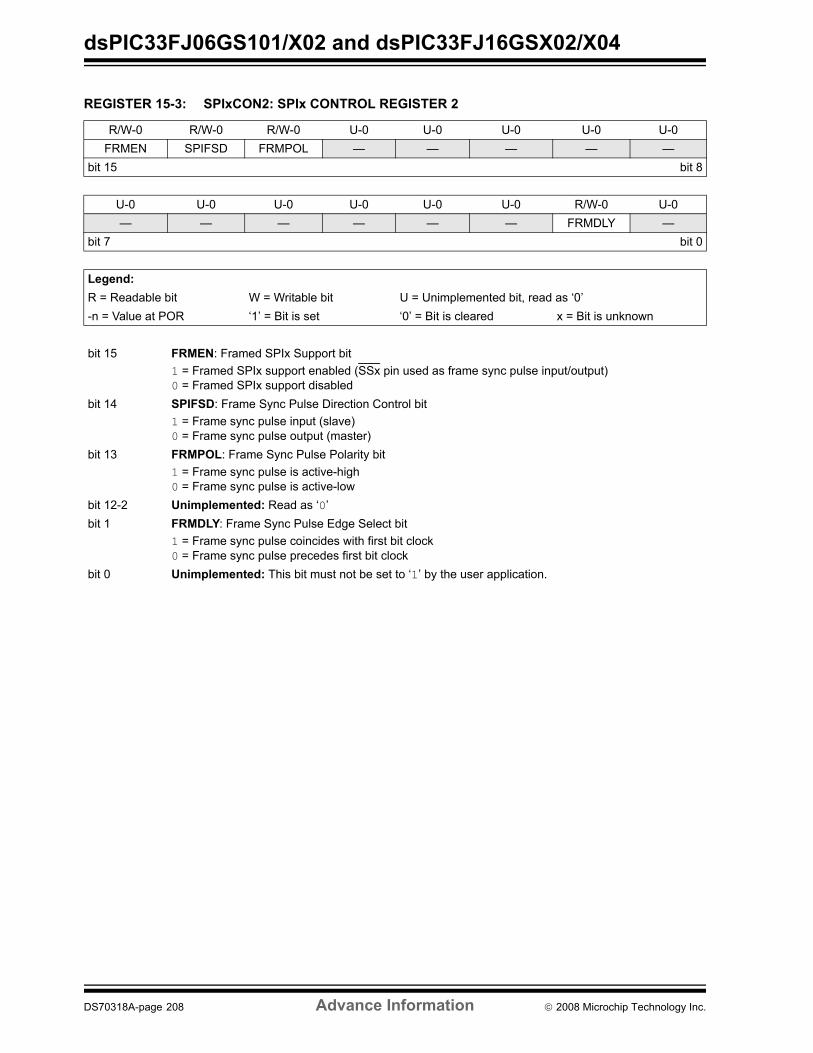
dsPIC33FJ06GS101/X02 and dsPIC33FJ16GSX02/X04
REGISTER 15-3: SPIxCON2: SPIx CONTROL REGISTER 2
R/W-0 R/W-0 R/W-0 U-0 U-0 U-0 U-0 U-0FRMEN SPIFSD FRMPOL — — — — —
bit 15 bit 8
U-0 U-0 U-0 U-0 U-0 U-0 R/W-0 U-0— — — — — — FRMDLY —
bit 7 bit 0
Legend:R = Readable bit W = Writable bit U = Unimplemented bit, read as ‘0’-n = Value at POR ‘1’ = Bit is set ‘0’ = Bit is cleared x = Bit is unknown
bit 15 FRMEN: Framed SPIx Support bit1 = Framed SPIx support enabled (SSx pin used as frame sync pulse input/output)0 = Framed SPIx support disabled
bit 14 SPIFSD: Frame Sync Pulse Direction Control bit1 = Frame sync pulse input (slave)0 = Frame sync pulse output (master)
bit 13 FRMPOL: Frame Sync Pulse Polarity bit1 = Frame sync pulse is active-high0 = Frame sync pulse is active-low
bit 12-2 Unimplemented: Read as ‘0’bit 1 FRMDLY: Frame Sync Pulse Edge Select bit
1 = Frame sync pulse coincides with first bit clock0 = Frame sync pulse precedes first bit clock
bit 0 Unimplemented: This bit must not be set to ‘1’ by the user application.
DS70318A-page 208 Advance Information © 2008 Microchip Technology Inc.

dsPIC33FJ06GS101/X02 and dsPIC33FJ16GSX02/X04
16.0 INTER-INTEGRATED CIRCUIT (I2C™)
The Inter-Integrated Circuit (I2C) module providescomplete hardware support for both Slave andMulti-Master modes of the I2C serial communicationstandard, with a 16-bit interface.
The I2C module has a 2-pin interface:
• The SCLx pin is clock.• The SDAx pin is data.
The I2C module offers the following key features:
• I2C interface supporting both Master and Slave modes of operation.
• I2C Slave mode supports 7 and 10-bit address.• I2C Master mode supports 7 and 10-bit address.• I2C port allows bidirectional transfers between
master and slaves.• Serial clock synchronization for I2C port can be
used as a handshake mechanism to suspend and resume serial transfer (SCLREL control).
• I2C supports multi-master operation, detects bus collision and arbitrates accordingly.
16.1 Operating ModesThe hardware fully implements all the master and slavefunctions of the I2C Standard and Fast modespecifications, as well as 7 and 10-bit addressing.
The I2C module can operate either as a slave or amaster on an I2C bus.
The following types of I2C operation are supported:
• I2C slave operation with 7-bit address• I2C slave operation with 10-bit address• I2C master operation with 7- or 10-bit address
For details about the communication sequence in eachof these modes, refer to the “dsPIC33F FamilyReference Manual”. Please see the Microchip website(www.microchip.com) for the latest dsPIC33F FamilyReference Manual chapters.
16.2 I2C RegistersI2CxCON and I2CxSTAT are control and statusregisters, respectively. The I2CxCON register isreadable and writable. The lower six bits of I2CxSTATare read-only. The remaining bits of the I2CSTAT areread/write:
• I2CxRSR is the shift register used for shifting data internal to the module and the user application has no access to it.
• I2CxRCV is the receive buffer and the register to which data bytes are written, or from which data bytes are read.
• I2CxTRN is the transmit register to which bytes are written during a transmit operation.
• The I2CxADD register holds the slave address.• A status bit, ADD10, indicates 10-bit Address
mode. • The I2CxBRG acts as the Baud Rate Generator
(BRG) reload value.
In receive operations, I2CxRSR and I2CxRCV togetherform a double-buffered receiver. When I2CxRSRreceives a complete byte, it is transferred to I2CxRCV,and an interrupt pulse is generated.
16.3 I2C InterruptsThe I2C module generates two interrupts:
• MI2CxIF (I2C Master Events Interrupt flag)• SI2CxIF (I2C Slave Events Interrupt flag)
A separate interrupt is generated for all I2C error conditions.
16.4 Baud Rate Generator In I2C Master mode, the reload value for the Baud RateGenerator (BRG) is located in the I2CxBRG register.When the BRG is loaded with this value, the BRGcounts down to zero and stops until another reload hastaken place. If clock arbitration is taking place, forexample, the BRG is reloaded when the SCLx pin issampled high.
As per the I2C standard, FSCL can be 100 kHz or400 kHz. However, the user application can specify anybaud rate up to 1 MHz. I2CxBRG values of ‘0’ or ‘1’ areillegal.
EQUATION 16-1: SERIAL CLOCK RATE
Note: This data sheet summarizes the featuresof the dsPIC33FJ06GS101/X02 anddsPIC33FJ16GSX02/X04 families ofdevices. It is not intended to be acomprehensive reference source. Tocomplement the information in this datasheet, refer to the dsPIC33F FamilyReference Manual, “Section 19.Inter-Integrated Circuit (I2C™)”(DS70195), which is available on theMicrochip website (www.microchip.com).
I2CxBRG = FCY FCYFSCL 1,111,111 – 1–( )
© 2008 Microchip Technology Inc. Advance Information DS70318A-page 209

dsPIC33FJ06GS101/X02 and dsPIC33FJ16GSX02/X04
FIGURE 16-1: I2C™ BLOCK DIAGRAM (X = 1)
InternalData Bus
SCLx
SDAx
Shift
Match Detect
I2CxADD
Start and StopBit Detect
Clock
Address Match
ClockStretching
I2CxTRNLSb
Shift Clock
BRG Down Counter
ReloadControl
TCY/2
Start and StopBit Generation
AcknowledgeGeneration
CollisionDetect
I2CxCON
I2CxSTAT
Con
trol L
ogic
Read
LSb
Write
Read
I2CxBRG
I2CxRSR
Write
Read
Write
Read
Write
Read
Write
Read
Write
Read
I2CxMSK
I2CxRCV
DS70318A-page 210 Advance Information © 2008 Microchip Technology Inc.

dsPIC33FJ06GS101/X02 and dsPIC33FJ16GSX02/X04
16.5 I2C Module AddressesThe 10-bit I2CxADD register contains the Slave modeaddresses.
If the A10M bit (I2CxCON<10>) is ‘0’, the address isinterpreted by the module as a 7-bit address. When anaddress is received, it is compared with the 7 LeastSignificant bits of the I2CxADD register.
If the A10M bit is ‘1’, the address is assumed to be a10-bit address. When an address is received, it iscompared with the binary value, ‘11110 A9 A8’(where A9 and A8 are two Most Significant bits ofI2CxADD). If that value matches, the next address iscompared with the Least Significant 8 bits of I2CxADD,as specified in the 10-bit addressing protocol.
TABLE 16-1: SUPPORTED 7-BIT I2C™ SLAVE ADDRESSES
16.6 Slave Address MaskingThe I2CxMSK register (Register 16-3) designatesaddress bit positions as “don’t care” for both 7-bit and10-bit Address modes. Setting a particular bitlocation (= 1) in the I2CxMSK register causes the slavemodule to respond, whether the correspondingaddress bit value is a ‘0’ or ‘1’. For example, whenI2CxMSK is set to ‘00100000’, the Slave moduledetects both addresses, ‘0000000’ and ‘00100000’.
To enable address masking, the IPMI (IntelligentPeripheral Management Interface) must be disabled byclearing the IPMIEN bit (I2CxCON<11>).
16.7 IPMI SupportThe control bit IPMIEN enables the module to supportthe Intelligent Peripheral Management Interface (IPMI).When this bit is set, the module accepts and acts uponall addresses.
16.8 General Call Address SupportThe general call address can address all devices.When this address is used, all devices should, intheory, respond with an Acknowledgement.
The general call address is one of eight addressesreserved for specific purposes by the I2C protocol. Itconsists of all ‘0’s with R_W = 0.
The general call address is recognized when theGeneral Call Enable (GCEN) bit is set(I2CxCON<7> = 1). When the interrupt is serviced, thesource for the interrupt can be checked by reading thecontents of the I2CxRCV to determine if the addresswas device-specific or a general call address.
16.9 Automatic Clock StretchIn Slave modes, the module can synchronize bufferreads and write to the master device by clock stretching.
16.9.1 TRANSMIT CLOCK STRETCHINGBoth 10-bit and 7-bit Transmit modes implement clockstretching by asserting the SCLREL bit after the fallingedge of the ninth clock, if the TBF bit is cleared,indicating the buffer is empty.
In Slave Transmit modes, clock stretching is alwaysperformed, irrespective of the STREN bit. The user’sISR must set the SCLREL bit before transmission isallowed to continue. By holding the SCLx line low, theuser application has time to service the ISR and loadthe contents of the I2CxTRN before the master devicecan initiate another transmit sequence.
16.9.2 RECEIVE CLOCK STRETCHINGThe STREN bit in the I2CxCON register can be used toenable clock stretching in Slave Receive mode. Whenthe STREN bit is set, the SCLx pin is held low at theend of each data receive sequence.
The user’s ISR must set the SCLREL bit beforereception is allowed to continue. By holding the SCLxline low, the user application has time to service theISR and read the contents of the I2CxRCV before themaster device can initiate another receive sequence.This prevents buffer overruns.
16.10 Software Controlled Clock Stretching (STREN = 1)
When the STREN bit is ‘1’, the software can clear theSCLREL bit to allow software to control the clockstretching.
If the STREN bit is ‘0’, a software write to the SCLRELbit is disregarded and has no effect on the SCLREL bit.
Address Description
0x00 General call address or Start byte0x01-0x03 Reserved0x04-0x07 HS mode Master codes0x08-0x77 Valid 7-bit addresses0x78-0x7B Valid 10-bit addresses (lower 7 bits)0x7C-0x7F Reserved
© 2008 Microchip Technology Inc. Advance Information DS70318A-page 211

dsPIC33FJ06GS101/X02 and dsPIC33FJ16GSX02/X04
16.11 Slope ControlThe I2C standard requires slope control on the SDAxand SCLx signals for Fast mode (400 kHz). The controlbit, DISSLW, enables the user application to disableslew rate control if desired. It is necessary to disablethe slew rate control for 1 MHz mode.
16.12 Clock ArbitrationClock arbitration occurs when the master deasserts theSCLx pin (SCLx allowed to float high) during anyreceive, transmit or Restart/Stop condition. When theSCLx pin is allowed to float high, the Baud RateGenerator (BRG) is suspended from counting until theSCLx pin is actually sampled high. When the SCLx pinis sampled high, the BRG is reloaded with the contentsof I2CxBRG and begins counting. This processensures that the SCLx high time is always at least oneBRG rollover count in the event that the clock is heldlow by an external device.
16.13 Multi-Master Communication, Bus Collision and Bus Arbitration
Multi-Master mode support is achieved by busarbitration. When the master outputs address/data bitsonto the SDAx pin, arbitration takes place when themaster outputs a ‘1’ on SDAx by letting SDAx float highwhile another master asserts a ‘0’. When the SCLx pinfloats high, data should be stable. If the expected dataon SDAx is a ‘1’ and the data sampled on theSDAx pin = 0, then a bus collision has taken place. Themaster sets the I2C master events interrupt flag andresets the master portion of the I2C port to its Idle state.
DS70318A-page 212 Advance Information © 2008 Microchip Technology Inc.

dsPIC33FJ06GS101/X02 and dsPIC33FJ16GSX02/X04
REGISTER 16-1: I2CxCON: I2Cx CONTROL REGISTER
R/W-0 U-0 R/W-0 R/W-1 HC R/W-0 R/W-0 R/W-0 R/W-0I2CEN — I2CSIDL SCLREL IPMIEN A10M DISSLW SMEN
bit 15 bit 8
R/W-0 R/W-0 R/W-0 R/W-0 HC R/W-0 HC R/W-0 HC R/W-0 HC R/W-0 HCGCEN STREN ACKDT ACKEN RCEN PEN RSEN SEN
bit 7 bit 0
Legend: U = Unimplemented bit, read as ‘0’R = Readable bit W = Writable bit HS = Set in hardware HC = Cleared in hardware-n = Value at POR ‘1’ = Bit is set ‘0’ = Bit is cleared x = Bit is unknown
bit 15 I2CEN: I2Cx Enable bit 1 = Enables the I2Cx module and configures the SDAx and SCLx pins as serial port pins0 = Disables the I2Cx module. All I2C pins are controlled by port functions.
bit 14 Unimplemented: Read as ‘0’bit 13 I2CSIDL: Stop in Idle Mode bit
1 = Discontinue module operation when device enters an Idle mode0 = Continue module operation in Idle mode
bit 12 SCLREL: SCLx Release Control bit (when operating as I2C slave)1 = Release SCLx clock0 = Hold SCLx clock low (clock stretch)If STREN = 1: Bit is R/W (i.e., software can write ‘0’ to initiate stretch and write ‘1’ to release clock). Hardware clearat beginning of slave transmission. Hardware clear at end of slave reception.If STREN = 0: Bit is R/S (i.e., software can only write ‘1’ to release clock). Hardware clear at beginning of slavetransmission.
bit 11 IPMIEN: Intelligent Peripheral Management Interface (IPMI) Enable bit1 = IPMI mode is enabled; all addresses Acknowledged0 = IPMI mode disabled
bit 10 A10M: 10-bit Slave Address bit1 = I2CxADD is a 10-bit slave address0 = I2CxADD is a 7-bit slave address
bit 9 DISSLW: Disable Slew Rate Control bit1 = Slew rate control disabled0 = Slew rate control enabled
bit 8 SMEN: SMbus Input Levels bit1 = Enable I/O pin thresholds compliant with SMbus specification0 = Disable SMbus input thresholds
bit 7 GCEN: General Call Enable bit (when operating as I2C slave)1 = Enable interrupt when a general call address is received in the I2CxRSR
(module is enabled for reception)0 = General call address disabled
bit 6 STREN: SCLx Clock Stretch Enable bit (when operating as I2C slave)Used in conjunction with SCLREL bit.1 = Enable software or receive clock stretching0 = Disable software or receive clock stretching
© 2008 Microchip Technology Inc. Advance Information DS70318A-page 213

dsPIC33FJ06GS101/X02 and dsPIC33FJ16GSX02/X04
bit 5 ACKDT: Acknowledge Data bit (when operating as I2C master, applicable during master receive)Value that is transmitted when the software initiates an Acknowledge sequence.1 = Send NACK during Acknowledge0 = Send ACK during Acknowledge
bit 4 ACKEN: Acknowledge Sequence Enable bit (when operating as I2C master, applicable during master receive)1 = Initiate Acknowledge sequence on SDAx and SCLx pins and transmit ACKDT data bit.
Hardware clear at end of master Acknowledge sequence.0 = Acknowledge sequence not in progress
bit 3 RCEN: Receive Enable bit (when operating as I2C master)1 = Enables Receive mode for I2C. Hardware clear at end of eighth bit of master receive data byte.0 = Receive sequence not in progress
bit 2 PEN: Stop Condition Enable bit (when operating as I2C master)1 = Initiate Stop condition on SDAx and SCLx pins. Hardware clear at end of master Stop sequence.0 = Stop condition not in progress
bit 1 RSEN: Repeated Start Condition Enable bit (when operating as I2C master)1 = Initiate Repeated Start condition on SDAx and SCLx pins. Hardware clear at end of
master Repeated Start sequence.0 = Repeated Start condition not in progress
bit 0 SEN: Start Condition Enable bit (when operating as I2C master)1 = Initiate Start condition on SDAx and SCLx pins. Hardware clear at end of master Start sequence.0 = Start condition not in progress
REGISTER 16-1: I2CxCON: I2Cx CONTROL REGISTER (CONTINUED)
DS70318A-page 214 Advance Information © 2008 Microchip Technology Inc.
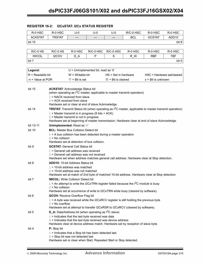
dsPIC33FJ06GS101/X02 and dsPIC33FJ16GSX02/X04
REGISTER 16-2: I2CxSTAT: I2Cx STATUS REGISTER
R-0 HSC R-0 HSC U-0 U-0 U-0 R/C-0 HSC R-0 HSC R-0 HSCACKSTAT TRSTAT — — — BCL GCSTAT ADD10
bit 15 bit 8
R/C-0 HS R/C-0 HS R-0 HSC R/C-0 HSC R/C-0 HSC R-0 HSC R-0 HSC R-0 HSCIWCOL I2COV D_A P S R_W RBF TBF
bit 7 bit 0
Legend: U = Unimplemented bit, read as ‘0’R = Readable bit W = Writable bit HS = Set in hardware HSC = Hardware set/cleared-n = Value at POR ‘1’ = Bit is set ‘0’ = Bit is cleared x = Bit is unknown
bit 15 ACKSTAT: Acknowledge Status bit (when operating as I2C master, applicable to master transmit operation)1 = NACK received from slave0 = ACK received from slaveHardware set or clear at end of slave Acknowledge.
bit 14 TRSTAT: Transmit Status bit (when operating as I2C master, applicable to master transmit operation)1 = Master transmit is in progress (8 bits + ACK)0 = Master transmit is not in progressHardware set at beginning of master transmission. Hardware clear at end of slave Acknowledge.
bit 13-11 Unimplemented: Read as ‘0’bit 10 BCL: Master Bus Collision Detect bit
1 = A bus collision has been detected during a master operation0 = No collisionHardware set at detection of bus collision.
bit 9 GCSTAT: General Call Status bit1 = General call address was received0 = General call address was not receivedHardware set when address matches general call address. Hardware clear at Stop detection.
bit 8 ADD10: 10-bit Address Status bit1 = 10-bit address was matched0 = 10-bit address was not matchedHardware set at match of 2nd byte of matched 10-bit address. Hardware clear at Stop detection.
bit 7 IWCOL: Write Collision Detect bit1 = An attempt to write the I2CxTRN register failed because the I2C module is busy 0 = No collisionHardware set at occurrence of write to I2CxTRN while busy (cleared by software).
bit 6 I2COV: Receive Overflow Flag bit1 = A byte was received while the I2CxRCV register is still holding the previous byte0 = No overflowHardware set at attempt to transfer I2CxRSR to I2CxRCV (cleared by software).
bit 5 D_A: Data/Address bit (when operating as I2C slave)1 = Indicates that the last byte received was data0 = Indicates that the last byte received was device addressHardware clear at device address match. Hardware set by reception of slave byte.
bit 4 P: Stop bit 1 = Indicates that a Stop bit has been detected last0 = Stop bit was not detected lastHardware set or clear when Start, Repeated Start or Stop detected.
© 2008 Microchip Technology Inc. Advance Information DS70318A-page 215

dsPIC33FJ06GS101/X02 and dsPIC33FJ16GSX02/X04
bit 3 S: Start bit 1 = Indicates that a Start (or Repeated Start) bit has been detected last0 = Start bit was not detected lastHardware set or clear when Start, Repeated Start or Stop detected.
bit 2 R_W: Read/Write Information bit (when operating as I2C slave)1 = Read – indicates data transfer is output from slave0 = Write – indicates data transfer is input to slaveHardware set or clear after reception of I2C device address byte.
bit 1 RBF: Receive Buffer Full Status bit 1 = Receive complete, I2CxRCV is full0 = Receive not complete, I2CxRCV is emptyHardware set when I2CxRCV is written with received byte. Hardware clear when software readsI2CxRCV.
bit 0 TBF: Transmit Buffer Full Status bit1 = Transmit in progress, I2CxTRN is full0 = Transmit complete, I2CxTRN is emptyHardware set when software writes I2CxTRN. Hardware clear at completion of data transmission.
REGISTER 16-2: I2CxSTAT: I2Cx STATUS REGISTER (CONTINUED)
DS70318A-page 216 Advance Information © 2008 Microchip Technology Inc.

dsPIC33FJ06GS101/X02 and dsPIC33FJ16GSX02/X04
REGISTER 16-3: I2CxMSK: I2Cx SLAVE MODE ADDRESS MASK REGISTER
U-0 U-0 U-0 U-0 U-0 U-0 R/W-0 R/W-0— — — — — — AMSK9 AMSK8
bit 15 bit 8
R/W-0 R/W-0 R/W-0 R/W-0 R/W-0 R/W-0 R/W-0 R/W-0AMSK7 AMSK6 AMSK5 AMSK4 AMSK3 AMSK2 AMSK1 AMSK0
bit 7 bit 0
Legend:R = Readable bit W = Writable bit U = Unimplemented bit, read as ‘0’-n = Value at POR ‘1’ = Bit is set ‘0’ = Bit is cleared x = Bit is unknown
bit 15-10 Unimplemented: Read as ‘0’bit 9-0 AMSKx: Mask for Address bit x Select bit
1 = Enable masking for bit x of incoming message address; bit match not required in this position0 = Disable masking for bit x; bit match required in this position
© 2008 Microchip Technology Inc. Advance Information DS70318A-page 217

dsPIC33FJ06GS101/X02 and dsPIC33FJ16GSX02/X04
NOTES:
DS70318A-page 218 Advance Information © 2008 Microchip Technology Inc.

dsPIC33FJ06GS101/X02 and dsPIC33FJ16GSX02/X04
17.0 UNIVERSAL ASYNCHRONOUS RECEIVER TRANSMITTER (UART)
The Universal Asynchronous Receiver Transmitter(UART) module is one of the serial I/O modulesavailable in the dsPIC33FJ06GS101/X02 anddsPIC33FJ16GSX02/X04 device family. The UART is afull-duplex asynchronous system that cancommunicate with peripheral devices, such aspersonal computers, LIN, RS-232 and RS-485interfaces. The module also supports a hardware flowcontrol option with the UxCTS and UxRTS pins andalso includes an IrDA® encoder and decoder.
The primary features of the UART module are:
• Full-Duplex, 8- or 9-bit Data Transmission through the UxTX and UxRX pins
• Even, Odd or No Parity Options (for 8-bit data)• One or two stop bits
• Hardware flow control option with UxCTS and UxRTS pins
• Fully integrated Baud Rate Generator with 16-bit prescaler
• Baud rates ranging from 1 Mbps to 15 bps at 16xmode at 40 MIPS
• Baud rates ranging from 4 Mbps to 61 bps at 4xmode at 40 MIPS
• 4-deep First-In First-Out (FIFO) Transmit Databuffer
• 4-deep FIFO Receive Data buffer• Parity, framing and buffer overrun error detection• Support for 9-bit mode with Address Detect
(9th bit = 1)• Transmit and Receive interrupts• A separate interrupt for all UART error conditions• Loopback mode for diagnostic support• Support for sync and break characters• Support for automatic baud rate detection• IrDA encoder and decoder logic• 16x baud clock output for IrDA support• Support for DMA
A simplified block diagram of the UART module isshown in Figure 17-1. The UART module consists ofthese key hardware elements:
• Baud Rate Generator• Asynchronous Transmitter• Asynchronous Receiver
FIGURE 17-1: UART SIMPLIFIED BLOCK DIAGRAM
Note: This data sheet summarizes the featuresof the dsPIC33FJ06GS101/X02 anddsPIC33FJ16GSX02/X04 families ofdevices. It is not intended to be acomprehensive reference source. Tocomplement the information in this datasheet, refer to the dsPIC33F FamilyReference Manual, “Section 17. UART”(DS70188), which is available on theMicrochip website (www.microchip.com).
UxRX
Hardware Flow Control
UART Receiver
UART Transmitter UxTX
Baud Rate Generator
UxRTS
IrDA®
UxCTS
© 2008 Microchip Technology Inc. Advance Information DS70318A-page 219

dsPIC33FJ06GS101/X02 and dsPIC33FJ16GSX02/X04
17.1 UART Baud Rate Generator (BRG)The UART module includes a dedicated 16-bit BaudRate Generator (BRG). The BRGx register controls theperiod of a free-running 16-bit timer. Equation 17-1shows the formula for computation of the baud ratewith BRGH = 0.
EQUATION 17-1: UART BAUD RATE WITH BRGH = 0
Example 17-1 shows the calculation of the baud rateerror for the following conditions:
• FCY = 4 MHz • Desired Baud Rate = 9600
The maximum baud rate (BRGH = 0) possible isFCY/16 (for BRGx = 0), and the minimum baud ratepossible is FCY/(16 * 65536).
Equation 17-2 shows the formula for computation ofthe baud rate with BRGH = 1.
EQUATION 17-2: UART BAUD RATE WITH BRGH = 1
The maximum baud rate (BRGH = 1) possible is FCY/4(for BRGx = 0), and the minimum baud rate possible isFCY/(4 * 65536).
Writing a new value to the BRGx register causes theBRG timer to be reset (cleared). This ensures the BRGdoes not wait for a timer overflow before generating thenew baud rate.
EXAMPLE 17-1: BAUD RATE ERROR CALCULATION (BRGH = 0)
Note: FCY denotes the instruction cycle clockfrequency (FOSC/2).
Baud Rate = FCY
16 • (BRGx + 1)
FCY16 • Baud Rate
BRGx = – 1
Note: FCY denotes the instruction cycle clockfrequency (FOSC/2).
Baud Rate = FCY
4 • (BRGx + 1)
FCY4 • Baud Rate
BRGx = – 1
Desired Baud Rate = FCY/(16 (BRGx + 1)) Solving for BRGx Value:
BRGx = ((FCY/Desired Baud Rate)/16) – 1BRGx = ((4000000/9600)/16) – 1 BRGx = 25
Calculated Baud Rate = 4000000/(16 (25 + 1)) = 9615
Error = (Calculated Baud Rate – Desired Baud Rate)Desired Baud Rate
= (9615 – 9600)/9600 = 0.16%
DS70318A-page 220 Advance Information © 2008 Microchip Technology Inc.

dsPIC33FJ06GS101/X02 and dsPIC33FJ16GSX02/X04
17.2 Transmitting in 8-bit Data ModeComplete the following steps to transmit data in 8-bitdata mode:
1. Set up the UART:a) Write appropriate values for data, parity and
Stop bits.b) Write appropriate baud rate value to the
BRGx register.c) Set up transmit and receive interrupt enable
and priority bits.2. Enable the UART.3. Set the UTXEN bit (causes a transmit interrupt).4. Write data byte to lower byte of UxTXREG word.
The value will be immediately transferred to theTransmit Shift Register (TSR) and the serial bitstream will start shifting out with the next risingedge of the baud clock.
A transmit interrupt will be generated as per theinterrupt control bits, UTXISEL<1:0>.
17.3 Transmitting in 9-bit Data ModeComplete the following steps to transmit data in 9-bitdata mode:
1. Set up the UART (as described in Section 17.2“Transmitting in 8-bit Data Mode”).
2. Enable the UART.3. Set the UTXEN bit (causes a transmit interrupt).4. Write UxTXREG as a 16-bit value only.
A word write to UxTXREG triggers the transferof the 9-bit data to the TSR. The serial bit streamwill start shifting out with the first rising edge ofthe baud clock.
A transmit interrupt will be generated as per thesetting of control bits, UTXISEL<1:0>.
17.4 Break and Sync Transmit Sequence
The following sequence will send a message frameheader made up of a Break, followed by an auto-baudSync byte.
1. Configure the UART for the desired mode.2. Set UTXEN and UTXBRK, which sets up the
Break character.3. Load the UxTXREG register with a dummy
character to initiate transmission (value isignored).
Write 0x55 to UxTXREG, which loads the Synccharacter into the transmit FIFO. After the Break hasbeen sent, the UTXBRK bit is reset by hardware. TheSync character now transmits.
17.5 Receiving in 8-bit or 9-bit Data Mode
Complete the following steps to receive data in 8-bit or9-bit data mode:
1. Set up the UART (as described in Section 17.2“Transmitting in 8-bit Data Mode”).
2. Enable the UART.A receive interrupt will be generated when oneor more data characters have been received asper interrupt control bits, URXISEL<1:0>.
3. Read the OERR bit to determine if an overrunerror has occurred. The OERR bit must be resetin software.
4. Read UxRXREG.
The act of reading the UxRXREG character will movethe next character to the top of the receive FIFO,including a new set of PERR and FERR values.
17.6 Flow Control Using UxCTS and UxRTS Pins
UARTx Clear to Send (UxCTS) and Request to Send(UxRTS) are the two hardware controlled active-lowpins associated with the UART module. The UEN<1:0>bits in the UxMODE register configures these pins. These two pins allow the UART to operate in Simplexand Flow Control modes. They are implemented tocontrol the transmission and the reception between theData Terminal Equipment (DTE).
17.7 Infrared SupportThe UART module provides two types of infrared UARTsupport:
• IrDA clock output to support external IrDA encoder and decoder device (legacy module support)
• Full implementation of the IrDA encoder and decoder
17.7.1 EXTERNAL IrDA SUPPORT – IrDA CLOCK OUTPUT
To support external IrDA encoder and decoder devices,the BCLK pin (same as the UxRTS pin) can beconfigured to generate the 16x baud clock. WithUEN<1:0> = 11, the BCLK pin will output the 16x baudclock if the UART module is enabled. The pin can beused to support the IrDA codec chip.
17.7.2 BUILT-IN IrDA ENCODER AND DECODER
The UART module includes full implementation of theIrDA encoder and decoder. The built-in IrDA encoderand decoder functionality is enabled using the IREN bit(UxMODE<12>). When enabled (IREN = 1), thereceive pin (UxRX) acts as the input from the infraredreceiver. The transmit pin (UxTX) acts as the output tothe infrared transmitter.
© 2008 Microchip Technology Inc. Advance Information DS70318A-page 221

dsPIC33FJ06GS101/X02 and dsPIC33FJ16GSX02/X04
REGISTER 17-1: UxMODE: UARTx MODE REGISTER
R/W-0 U-0 R/W-0 R/W-0 R/W-0 U-0 R/W-0 R/W-0UARTEN — USIDL IREN(1) RTSMD — UEN<1:0>
bit 15 bit 8
R/W-0 HC R/W-0 R/W-0 HC R/W-0 R/W-0 R/W-0 R/W-0 R/W-0WAKE LPBACK ABAUD URXINV BRGH PDSEL<1:0> STSEL
bit 7 bit 0
Legend: HC = Cleared in HardwareR = Readable bit W = Writable bit U = Unimplemented bit, read as ‘0’-n = Value at POR ‘1’ = Bit is set ‘0’ = Bit is cleared x = Bit is unknown
bit 15 UARTEN: UARTx Enable bit1 = UARTx is enabled; all UARTx pins are controlled by UARTx as defined by UEN<1:0>0 = UARTx is disabled; all UARTx pins are controlled by port latches; UARTx power consumption
minimalbit 14 Unimplemented: Read as ‘0’bit 13 USIDL: Stop in Idle Mode bit
1 = Discontinue module operation when device enters Idle mode0 = Continue module operation in Idle mode
bit 12 IREN: IrDA Encoder and Decoder Enable bit(1)
1 = IrDA encoder and decoder enabled0 = IrDA encoder and decoder disabled
bit 11 RTSMD: Mode Selection for UxRTS Pin bit1 = UxRTS pin in Simplex mode0 = UxRTS pin in Flow Control mode
bit 10 Unimplemented: Read as ‘0’bit 9-8 UEN<1:0>: UARTx Enable bits
11 = UxTX, UxRX and BCLK pins are enabled and used; UxCTS pin controlled by port latches10 = UxTX, UxRX, UxCTS and UxRTS pins are enabled and used01 = UxTX, UxRX and UxRTS pins are enabled and used; UxCTS pin controlled by port latches00 = UxTX and UxRX pins are enabled and used; UxCTS and UxRTS/BCLK pins controlled by
port latchesbit 7 WAKE: Wake-up on Start bit Detect During Sleep Mode Enable bit
1 = UARTx will continue to sample the UxRX pin; interrupt generated on falling edge; bit cleared in hardware on following rising edge
0 = No wake-up enabledbit 6 LPBACK: UARTx Loopback Mode Select bit
1 = Enable Loopback mode0 = Loopback mode is disabled
bit 5 ABAUD: Auto-Baud Enable bit1 = Enable baud rate measurement on the next character – requires reception of a Sync field (55h)
before other data; cleared in hardware upon completion0 = Baud rate measurement disabled or completed
bit 4 URXINV: Receive Polarity Inversion bit 1 = UxRX Idle state is ‘0’0 = UxRX Idle state is ‘1’
Note 1: This feature is only available for the 16x BRG mode (BRGH = 0).
DS70318A-page 222 Advance Information © 2008 Microchip Technology Inc.

dsPIC33FJ06GS101/X02 and dsPIC33FJ16GSX02/X04
bit 3 BRGH: High Baud Rate Enable bit1 = BRG generates 4 clocks per bit period (4x baud clock, High-Speed mode)0 = BRG generates 16 clocks per bit period (16x baud clock, Standard mode)
bit 2-1 PDSEL<1:0>: Parity and Data Selection bits11 = 9-bit data, no parity10 = 8-bit data, odd parity01 = 8-bit data, even parity00 = 8-bit data, no parity
bit 0 STSEL: Stop Bit Selection bit1 = Two Stop bits0 = One Stop bit
REGISTER 17-1: UxMODE: UARTx MODE REGISTER (CONTINUED)
Note 1: This feature is only available for the 16x BRG mode (BRGH = 0).
© 2008 Microchip Technology Inc. Advance Information DS70318A-page 223

dsPIC33FJ06GS101/X02 and dsPIC33FJ16GSX02/X04
REGISTER 17-2: UxSTA: UARTx STATUS AND CONTROL REGISTER
R/W-0 R/W-0 R/W-0 U-0 R/W-0 HC R/W-0 R-0 R-1UTXISEL1 UTXINV(1) UTXISEL0 — UTXBRK UTXEN UTXBF TRMT
bit 15 bit 8
R/W-0 R/W-0 R/W-0 R-1 R-0 R-0 R/C-0 R-0URXISEL<1:0> ADDEN RIDLE PERR FERR OERR URXDA
bit 7 bit 0
Legend: HC = Cleared in HardwareR = Readable bit W = Writable bit U = Unimplemented bit, read as ‘0’-n = Value at POR ‘1’ = Bit is set ‘0’ = Bit is cleared x = Bit is unknown
bit 15,13 UTXISEL<1:0>: Transmission Interrupt Mode Selection bits 11 = Reserved; do not use10 = Interrupt when a character is transferred to the Transmit Shift Register, and as a result, the
transmit buffer becomes empty01 = Interrupt when the last character is shifted out of the Transmit Shift Register; all transmit
operations are completed00 = Interrupt when a character is transferred to the Transmit Shift Register (this implies there is
at least one character open in the transmit buffer)bit 14 UTXINV: IrDA® Encoder Transmit Polarity Inversion bit(1)
1 = IrDA encoded, UxTX Idle state is ‘1’0 = IrDA encoded, UxTX Idle state is ‘0’
bit 12 Unimplemented: Read as ‘0’bit 11 UTXBRK: Transmit Break bit
1 = Send Sync Break on next transmission – Start bit, followed by twelve ‘0’ bits, followed by Stop bit;cleared by hardware upon completion
0 = Sync Break transmission disabled or completedbit 10 UTXEN: Transmit Enable bit
1 = Transmit enabled, UxTX pin controlled by UARTx0 = Transmit disabled, any pending transmission is aborted and buffer is reset. UxTX pin controlled
by port.bit 9 UTXBF: Transmit Buffer Full Status bit (read-only)
1 = Transmit buffer is full0 = Transmit buffer is not full, at least one more character can be written
bit 8 TRMT: Transmit Shift Register Empty bit (read-only)1 = Transmit Shift Register is empty and transmit buffer is empty (the last transmission has completed)0 = Transmit Shift Register is not empty, a transmission is in progress or queued
bit 7-6 URXISEL<1:0>: Receive Interrupt Mode Selection bits 11 = Interrupt is set on UxRSR transfer making the receive buffer full (i.e., has 4 data characters)10 = Interrupt is set on UxRSR transfer making the receive buffer 3/4 full (i.e., has 3 data characters)0x = Interrupt is set when any character is received and transferred from the UxRSR to the receive
buffer. Receive buffer has one or more characters.bit 5 ADDEN: Address Character Detect bit (bit 8 of received data = 1)
1 = Address Detect mode enabled. If 9-bit mode is not selected, this does not take effect.0 = Address Detect mode disabled
Note 1: Value of bit only affects the transmit properties of the module when the IrDA encoder is enabled (IREN = 1).
DS70318A-page 224 Advance Information © 2008 Microchip Technology Inc.

dsPIC33FJ06GS101/X02 and dsPIC33FJ16GSX02/X04
bit 4 RIDLE: Receiver Idle bit (read-only)1 = Receiver is Idle0 = Receiver is active
bit 3 PERR: Parity Error Status bit (read-only)1 = Parity error has been detected for the current character (character at the top of the receive FIFO)0 = Parity error has not been detected
bit 2 FERR: Framing Error Status bit (read-only)1 = Framing error has been detected for the current character (character at the top of the receive
FIFO)0 = Framing error has not been detected
bit 1 OERR: Receive Buffer Overrun Error Status bit (read-/clear-only)1 = Receive buffer has overflowed0 = Receive buffer has not overflowed. Clearing a previously set OERR bit (1 → 0 transition) will reset
the receiver buffer and the UxRSR to the empty state.bit 0 URXDA: Receive Buffer Data Available bit (read-only)
1 = Receive buffer has data, at least one more character can be read0 = Receive buffer is empty
REGISTER 17-2: UxSTA: UARTx STATUS AND CONTROL REGISTER (CONTINUED)
Note 1: Value of bit only affects the transmit properties of the module when the IrDA encoder is enabled (IREN = 1).
© 2008 Microchip Technology Inc. Advance Information DS70318A-page 225

dsPIC33FJ06GS101/X02 and dsPIC33FJ16GSX02/X04
NOTES:
DS70318A-page 226 Advance Information © 2008 Microchip Technology Inc.

dsPIC33FJ06GS101/X02 and dsPIC33FJ16GSX02/X04
18.0 HIGH-SPEED 10-BIT ANALOG-TO-DIGITAL CONVERTER (ADC)
The dsPIC33FJ06GS101/X02 and dsPIC33FJ16GSX02/X04 devices provide high-speed successiveapproximation analog to digital conversions to supportapplications such as AC/DC and DC/DC powerconverters.
18.1 Features OverviewThe ADC module incorporates following features:
• 10-bit resolution• Unipolar inputs• Up to two successive approximation registers
(SARs)• Up to 12 external input channels• Up to two internal analog inputs• Dedicated result register for each analog input• ±1 LSB accuracy at 3.3V• Single supply operation• 4 Msps conversion rate at 3.3V (devices with two
SARs)• 2 Msps conversion rate at 3.3V (devices with one
SAR)• Low-Power CMOS technology
18.2 Module DescriptionThis ADC module is designed for applications thatrequire low latency between the request for conversionand the resultant output data. Typical applicationsinclude:
• AC/DC power supplies• DC/DC converters• Power Factor Correction (PFC)
This ADC works with the High-Speed PWM module inpower control applications that require high-frequencycontrol loops. This module can sample and convert twoanalog inputs in 0.5 microsecond when two SARs areused. This small conversion delay reduces the “phaselag” between measurement and control systemresponse.
Up to five inputs may be sampled at a time (four inputsfrom the dedicated Sample and Hold circuits and onefrom the shared Sample and Hold circuit). If multipleinputs request conversion, the ADC will convert them ina sequential manner starting with the lowest orderinput.
This ADC design provides each pair of analog inputs(AN1,AN0), (AN3,AN2),..., the ability to specify its owntrigger source out of a maximum of sixteen differenttrigger sources. This capability allows this ADC to sam-ple and convert analog inputs that are associated withPWM generators operating on independent timebases.The user application typically requires synchronizationbetween analog data sampling and PWM output to theapplication circuit. The very high speed operation ofthis ADC module allows “data on demand”. In addition, several hardware features have beenadded to the peripheral interface to improve real-timeperformance in a typical DSP based application.• Result alignment options• Automated sampling• External conversion start control• Two internal inputs to monitor 1.2V internal
reference and EXTREF input signalA block diagram of the ADC module is shown in Figure 18-6.
Note: This data sheet summarizes the featuresof the dsPIC33FJ06GS101/X02 anddsPIC33FJ16GSX02/X04 families ofdevices. It is not intended to be acomprehensive reference source. Tocomplement the information in this datasheet, refer to the dsPIC33F FamilyReference Manual, “Section 44. High-Speed 10-bit Analog-to-DigitalConverter (ADC)” (DS70321), which isavailable on the Microchip website(www.microchip.com).
© 2008 Microchip Technology Inc. Advance Information DS70318A-page 227

dsPIC33FJ06GS101/X02 and dsPIC33FJ16GSX02/X04
18.3 Module FunctionalityThe High-Speed 10-bit ADC is designed to supportpower conversion applications when used with theHigh-Speed PWM module. The ADC may have one ortwo SAR modules, depending on the device variant. Iftwo SARs are present on a device, two conversionscan be processed at a time, yielding 4 Msps conversionrate. If only one SAR is present on a device, only oneconversion can be processed at a time, yielding 2 Mspsconversion rate. The High-Speed 10-Bit ADC producestwo 10-bit conversion results in 0.5 microsecond.
The ADC module supports up to 12 external analoginputs and two internal analog inputs. To monitorreference voltage, two internal inputs AN12 and AN13are connected to the EXTREF and internal band gapvoltages (1.2V), respectively.
The analog reference voltage is defined as the devicesupply voltage (AVDD / AVSS).
The ADC module uses following Control and Statusregisters:
• A/D Control Register (ADCON)• A/D Status Register (ADSTAT)• A/D Base Register (ADBASE)• A/D Port Configuration Register (ADPCFG)• A/D Convert Pair Control Register 0 (ADCPC0)• A/D Convert Pair Control Register 1 (ADCPC1)• A/D Convert Pair Control Register 2 (ADCPC2)• A/D Convert Pair Control Register 3 (ADCPC3)
The ADCON register controls the operation of theADC module. The ADSTAT register displays thestatus of the conversion processes. The ADPCFGregisters configure the port pins as analog inputs oras digital I/O. The ADCPCx registers control thetriggering of the ADC conversions. See Register 18-1through Register 18-8 for detailed bit configurations.
Note: A unique feature of the ADC module is itsability to sample inputs in anasynchronous manner. Individual sampleand hold circuits can be triggeredindependently of each other.
DS70318A-page 228 Advance Information © 2008 Microchip Technology Inc.

dsPIC33FJ06GS101/X02 and dsPIC33FJ16GSX02/X04
FIGURE 18-1: ADC BLOCK DIAGRAM FOR dsPIC33FJ06GS101 DEVICES WITH ONE SAR
Even numbered inputs with dedicated
Shared Sample and Hold
Dat
aFo
rmat
SARCore
Eight
Registers16-bit
Sample and Hold (S&H) circuits
Bus
Inte
rface
AN0
AN1
AN3
AN6
AN7
AN2
© 2008 Microchip Technology Inc. Advance Information DS70318A-page 229

dsPIC33FJ06GS101/X02 and dsPIC33FJ16GSX02/X04
FIGURE 18-2: ADC BLOCK DIAGRAM FOR dsPIC33FJ06GS102 DEVICES WITH ONE SAR
Even numbered inputs with dedicated
Shared Sample and Hold
Dat
aFo
rmat
SARCore
Eight
Registers16-bit
Sample and Hold (S&H) circuits
Bus
Inte
rface
AN0
AN2
AN1
AN4
AN5
AN3
DS70318A-page 230 Advance Information © 2008 Microchip Technology Inc.

dsPIC33FJ06GS101/X02 and dsPIC33FJ16GSX02/X04
FIGURE 18-3: ADC BLOCK DIAGRAM FOR dsPIC33FJ06GS202 DEVICES WITH ONE SAR
AN12(1)
AN13(2)
Even numbered inputs with dedicated
Shared Sample and Hold
Dat
aFo
rmat
SARCore
Eight
Registers16-bit
Sample and Hold (S&H) circuits
Bus
Inte
rface
AN0
AN2
AN1
AN4
AN5
AN3
(INTREF)
(EXTREF)
Note 1: AN12 (EXTREF) is an internal analog input. To measure the voltage at AN12 (EXTREF), an analog compar-ator must be enabled and EXTREF must be selected as the comparator reference.
2: AN13 (INTREF) is an internal analog input and is not available on a pin.
© 2008 Microchip Technology Inc. Advance Information DS70318A-page 231

dsPIC33FJ06GS101/X02 and dsPIC33FJ16GSX02/X04
FIGURE 18-4: ADC BLOCK DIAGRAM FOR dsPIC33FJ16GS402/404 DEVICES WITH ONE SAR
Even numbered inputs with dedicated
Shared Sample and HoldD
ata
Form
at
SARCore
Ten
Registers16-bit
Sample and Hold (S&H) circuits
Bus
Inte
rface
AN0
AN2
AN1
AN5
AN6
AN7
AN3
AN4
DS70318A-page 232 Advance Information © 2008 Microchip Technology Inc.

dsPIC33FJ06GS101/X02 and dsPIC33FJ16GSX02/X04
FIGURE 18-5: ADC BLOCK DIAGRAM FOR dsPIC33FJ16GS502 DEVICES WITH TWO SARS
AN12(1)
AN13(2)
Even numbered inputs with dedicated
Odd numbered inputswith shared S&H
Even numbered inputswith shared S&H
Dat
aFo
rmat
SARCore
Five
Registers16-bit
SARCore
Sample and Hold (S&H) circuits
Bus
Inte
rface
AN0
AN2
AN6
AN1
AN3
Dat
aFo
rmat Five
Registers16-bit
AN4
AN5
AN7
(INTREF)
(EXTREF)
Note 1: AN12 (EXTREF) is an internal analog input. To measure the voltage at AN12 (EXTREF), an analog compar-ator must be enabled and EXTREF must be selected as the comparator reference.
2: AN13 (INTREF) is an internal analog input and is not available on a pin.
© 2008 Microchip Technology Inc. Advance Information DS70318A-page 233

dsPIC33FJ06GS101/X02 and dsPIC33FJ16GSX02/X04
FIGURE 18-6: ADC BLOCK DIAGRAM FOR dsPIC33FJ16GS504 DEVICES WITH TWO SARS
AN12(1)
AN13(2)
Even numbered inputs with dedicated
Odd numbered inputswith shared S&H
Even numbered inputswith shared S&H
Dat
aFo
rmat
SARCore
Seven
Registers16-bit
SARCore
Sample and Hold (S&H) circuits
Bus
Inte
rface
AN0
AN2
AN6
AN1
AN3
AN8
AN10
Dat
aFo
rmat Seven
Registers16-bit
AN4
AN5
AN7
AN9
AN11
(INTREF)
(EXTREF)
Note 1: AN12 (EXTREF) is an internal analog input. To measure the voltage at AN12 (EXTREF), an analogcomparator must be enabled and EXTREF must be selected as the comparator reference.
2: AN13 (INTREF) is an internal analog input and is not available on a pin.
DS70318A-page 234 Advance Information © 2008 Microchip Technology Inc.

dsPIC33FJ06GS101/X02 and dsPIC33FJ16GSX02/X04
REGISTER 18-1: A/D CONTROL REGISTER (ADCON)
R/W-0 U-0 R/W-0 R/W-0 U-0 R/W-0 U-0 R/W-0ADON — ADSIDL SLOWCLK — GSWTRG — FORM
bit 15 bit 8
R/W-0 R/W-0 R/W-0 R/W-0 U-0 R/W-0 R/W-1 R/W-1EIE(1) ORDER(1) SEQSAMP ASYNCSAMP — ADCS<2:0>
bit 7 bit 0
Legend:R = Readable bit W = Writable bit U = Unimplemented bit, read as ‘0’-n = Value at POR ‘1’ = Bit is set ‘0’ = Bit is cleared x = Bit is unknown
bit 15 ADON: A/D Operating Mode bit1 = A/D converter module is operating0 = A/D converter is off
bit 14 Unimplemented: Read as ‘0’ bit 13 ADSIDL: Stop in Idle Mode bit
1 = Discontinue module operation when device enters Idle mode0 = Continue module operation in Idle mode
bit 12 SLOWCLK: Enable The Slow Clock Divider bit1 = Use the clock divider for low frequency ADC input clock. This divider provides lower numerical
divide ratios to enable the fastest ADC operation with slower input clocks.0 = Use the clock divider for high frequency ADC input clock. This divider provides higher numerical
divide ratios.bit 11 Unimplemented: Read as ‘0’ bit 10 GSWTRG: Global Software Trigger bit
When this bit is set by the user, it will trigger conversions if selected by the TRGSRC<4:0> bits in theADCPCx registers. This bit must be cleared by the user prior to initiating another global trigger (i.e.,this bit is not auto-clearing).
bit 9 Unimplemented: Read as ‘0’bit 8 FORM: Data Output Format bit
1 = Fractional (DOUT = dddd dddd dd00 0000)0 = Integer (DOUT = 0000 00dd dddd dddd)
bit 7 EIE: Early Interrupt Enable bit(1)
1 = Interrupt is generated after first conversion is completed0 = Interrupt is generated after second conversion is completed
bit 6 ORDER: Conversion Order bit(1)
1 = Odd numbered analog input is converted first, followed by conversion of even numbered input0 = Even numbered analog input is converted first, followed by conversion of odd numbered input
bit 5 SEQSAMP: Sequential Sample Enable.1 = Shared Sample and Hold (S&H) circuit is sampled at the start of the second conversion if
ORDER = 0. If ORDER = 1, then the shared S&H is sampled at the start of the first conversion.0 = Shared S&H is sampled at the same time the dedicated S&H is sampled if the shared S&H is not
currently busy with an existing conversion process. If the shared S&H is busy at the time thededicated S&H is sampled, then the shared S&H will sample at the start of the new conversioncycle.
Note 1: This control bit can only be changed while ADC is disabled (ADON = 0).
© 2008 Microchip Technology Inc. Advance Information DS70318A-page 235

dsPIC33FJ06GS101/X02 and dsPIC33FJ16GSX02/X04
bit 4 ASYNCSAMP: Asynchronous Dedicated S&H Sampling Enable bit1 = The dedicated S&H is constantly sampling and then terminates sampling as soon as the trigger
pulse is detected. 0 = The dedicated S&H starts sampling when the trigger event is detected and completes the sampling
process in two ADC clock cycles.bit 3 Unimplemented: Read as ‘0’bit 2-0 ADCS<2:0>: A/D Conversion Clock Divider Select bits
If SLOWCLK = 0, the ADC clock divider operation is as follows(2):111 = FADC/14 110 = FADC/13 101 = FADC/12•••000 = FADC/7
If SLOWCLK = 1, the ADC clock divider operation is as follows:111 = FADC/8110 = FADC/7101 = FADC/6100 = FADC/5011 = FADC/4010 = FADC/3001 = FADC/2000 = FADC/1
REGISTER 18-1: A/D CONTROL REGISTER (ADCON) (CONTINUED)
Note 1: This control bit can only be changed while ADC is disabled (ADON = 0).
DS70318A-page 236 Advance Information © 2008 Microchip Technology Inc.

dsPIC33FJ06GS101/X02 and dsPIC33FJ16GSX02/X04
REGISTER 18-2: A/D STATUS REGISTER (ADSTAT)
U-0 U-0 U-0 U-0 U-0 U-0 U-0 U-0— — — — — — — —
bit 15 bit 8
U-0 R/C-0H-S
R/C-0H-S
R/C-0H-S
R/C-0H-S
R/C-0H-S
R/C-0H-S
R/C-0H-S
— P6RDY P5RDY P4RDY P3RDY P2RDY P1RDY P0RDYbit 7 bit 0
Legend:R = Readable bit W = Writable bit U = Unimplemented bit, read as ‘0’-n = Value at PORC = Clear in software
‘1’ = Bit is setH-S = Set by hardware
‘0’ = Bit is cleared x = Bit is unknown
bit 15-7 Unimplemented: Read as ‘0’bit 6 P6RDY: Conversion Data for Pair 6 Ready bit
Bit is set when data is ready in buffer, cleared when a ‘0’ is written to this bit.bit 5 P5RDY: Conversion Data for Pair 5 Ready bit
Bit is set when data is ready in buffer, cleared when a ‘0’ is written to this bit.bit 4 P4RDY: Conversion Data for Pair 4 Ready bit
Bit is set when data is ready in buffer, cleared when a ‘0’ is written to this bit.bit 3 P3RDY: Conversion Data for Pair 3 Ready bit
Bit is set when data is ready in buffer, cleared when a ‘0’ is written to this bit.bit 2 P2RDY: Conversion Data for Pair 2 Ready bit
Bit is set when data is ready in buffer, cleared when a ‘0’ is written to this bit.bit 1 P1RDY: Conversion Data for Pair 1 Ready bit
Bit is set when data is ready in buffer, cleared when a ‘0’ is written to this bit.bit 0 P0RDY: Conversion Data for Pair 0 Ready bit
Bit is set when data is ready in buffer, cleared when a ‘0’ is written to this bit.
© 2008 Microchip Technology Inc. Advance Information DS70318A-page 237

dsPIC33FJ06GS101/X02 and dsPIC33FJ16GSX02/X04
REGISTER 18-3: A/D BASE REGISTER (ADBASE)
R/W-0 R/W-0 R/W-0 R/W-0 R/W-0 R/W-0 R/W-0 R/W-0ADBASE<15:8>
bit 15 bit 8
R/W-0 R/W-0 R/W-0 R/W-0 R/W-0 R/W-0 R/W-0 U-0ADBASE<7:1> —
bit 7 bit 0
Legend:R = Readable bit W = Writable bit U = Unimplemented bit, read as ‘0’-n = Value at POR ‘1’ = Bit is set ‘0’ = Bit is cleared x = Bit is unknown
bit 15-1 ADC Base Register: This register contains the base address of the user’s ADC Interrupt Service Routine jump table. This register, when read, contains the sum of the ADBASE register contents and the encoded value of the PxRDY Status bits.
The encoder logic provides the bit number of the highest priority PxRDY bits where P0RDY is thehighest priority, and P6RDY is lowest priority.
bit 0 Unimplemented: Read as ‘0’
Note 1: The encoding results are shifted left two bits so bits 1-0 of the result are always zero.
2: As an alternative to using the ADBASE Register, the ADCP0-6 ADC Pair Conversion Complete Interruptscan be used to invoke A to D conversion completion routines for individual ADC input pairs.
REGISTER 18-4: A/D PORT CONFIGURATION REGISTER (ADPCFG)
U-0 U-0 U-0 U-0 R/W-0 R/W-0 R/W-0 R/W-0— — — — PCFG11 PCFG10 PCFG9 PCFG8
bit 15 bit 8
R/W-0 R/W-0 R/W-0 R/W-0 R/W-0 R/W-0 R/W-0 R/W-0PCFG7 PCFG6 PCFG5 PCFG4 PCFG3 PCFG2 PCFG1 PCFG0
bit 7 bit 0
Legend:R = Readable bit W = Writable bit U = Unimplemented bit, read as ‘0’-n = Value at POR ‘1’ = Bit is set ‘0’ = Bit is cleared x = Bit is unknown
bit 15-12 Unimplemented: Read as ‘0’bit 11-0 PCFG<11:0>: A/D Port Configuration Control bits
1 = Port pin in Digital mode, port read input enabled, A/D input multiplexor connected to AVSS0 = Port pin in Analog mode, port read input disabled, A/D samples pin voltage
DS70318A-page 238 Advance Information © 2008 Microchip Technology Inc.

dsPIC33FJ06GS101/X02 and dsPIC33FJ16GSX02/X04
REGISTER 18-5: A/D CONVERT PAIR CONTROL REGISTER 0 (ADCPC0)
R/W-0 R/W-0 R/W-0 R/W-0 R/W-0 R/W-0 R/W-0 R/W-0IRQEN1 PEND1 SWTRG1 TRGSRC1<4:0>
bit 15 bit 8
R/W-0 R/W-0 R/W-0 R/W-0 R/W-0 R/W-0 R/W-0 R/W-0IRQEN0 PEND0 SWTRG0 TRGSRC0<4:0>
bit 7 bit 0
Legend:R = Readable bit W = Writable bit U = Unimplemented bit, read as ‘0’-n = Value at POR ‘1’ = Bit is set ‘0’ = Bit is cleared x = Bit is unknown
bit 15 IRQEN1: Interrupt Request Enable 1 bit1 = Enable IRQ generation when requested conversion of channels AN3 and AN2 is completed0 = IRQ is not generated
bit 14 PEND1: Pending Conversion Status 1 bit 1 = Conversion of channels AN3 and AN2 is pending. Set when selected trigger is asserted0 = Conversion is complete
bit 13 SWTRG1: Software Trigger 1 bit1 = Start conversion of AN3 and AN2 (if selected in TRGSRC bits)(1).
bit 12-8 TRGSRC1<4:0>: Trigger 1 Source Selection bitsSelects trigger source for conversion of analog channels AN3 and AN2.00000 = No conversion enabled00001 = Individual software trigger selected00010 = Global software trigger selected00011 = PWM Special Event Trigger selected00100 = PWM Generator 1 primary trigger selected00101 = PWM Generator 2 primary trigger selected00110 = PWM Generator 3 primary trigger selected00111 = PWM Generator 4 primary trigger selected01000 = Reserved•••01100 = Timer1 period match01101 = Reserved01110 = PWM Generator 1 secondary trigger selected01111 = PWM Generator 2 secondary trigger selected10000 = PWM Generator 3 secondary trigger selected10001 = PWM Generator 4 secondary trigger selected10010 = Reserved•••10110 = Reserved10111 = PWM Generator 1 current-limit ADC trigger11000 = PWM Generator 2 current-limit ADC trigger11001 = PWM Generator 3 current-limit ADC trigger11010 = PWM Generator 4 current-limit ADC trigger11011 = Reserved•••11111 = Timer2 period match
Note 1: If other conversions are in progress, then conversion will be performed when the conversion resources areavailable. This bit will be reset when the PEND bit is set.
© 2008 Microchip Technology Inc. Advance Information DS70318A-page 239

dsPIC33FJ06GS101/X02 and dsPIC33FJ16GSX02/X04
bit 7 IRQEN0: Interrupt Request Enable 0 bit1 = Enable IRQ generation when requested conversion of channels AN1 and AN0 is completed0 = IRQ is not generated
bit 6 PEND0: Pending Conversion Status 0 bit1 = Conversion of channels AN1 and AN0 is pending. Set when selected trigger is asserted.0 = Conversion is complete
bit 5 SWTRG0: Software Trigger 0 bit1 = Start conversion of AN1 and AN0 (if selected by TRGSRC bits)(1).
bit 4-0 TRGSRC0<4:0>: Trigger 0 Source Selection bits
Selects trigger source for conversion of analog channels AN1 and AN0.00000 = No conversion enabled00001 = Individual software trigger selected00010 = Global software trigger selected00011 = PWM Special Event Trigger selected00100 = PWM Generator 1 primary trigger selected00101 = PWM Generator 2 primary trigger selected00110 = PWM Generator 3 primary trigger selected00111 = PWM Generator 4 primary trigger selected01000 = Reserved•••01101 = Timer1 period match01101 = Reserved01110 = PWM Generator 1 secondary trigger selected01111 = PWM Generator 2 secondary trigger selected10000 = PWM Generator 3 secondary trigger selected10001 = PWM Generator 4 secondary trigger selected10010 = Reserved•••10110 = Reserved10111 = PWM Generator 1 current-limit ADC trigger11000 = PWM Generator 2 current-limit ADC trigger11001 = PWM Generator 3 current-limit ADC trigger11010 = PWM Generator 4 current-limit ADC trigger11011 = Reserved•••11111 = Timer2 period match
REGISTER 18-5: A/D CONVERT PAIR CONTROL REGISTER 0 (ADCPC0) (CONTINUED)
Note 1: If other conversions are in progress, then conversion will be performed when the conversion resources areavailable. This bit will be reset when the PEND bit is set.
DS70318A-page 240 Advance Information © 2008 Microchip Technology Inc.

dsPIC33FJ06GS101/X02 and dsPIC33FJ16GSX02/X04
REGISTER 18-6: A/D CONVERT PAIR CONTROL REGISTER 1 (ADCPC1)
R/W-0 R/W-0 R/W-0 R/W-0 R/W-0 R/W-0 R/W-0 R/W-0IRQEN3 PEND3 SWTRG3 TRGSRC3<4:0>
bit 15 bit 8
R/W-0 R/W-0 R/W-0 R/W-0 R/W-0 R/W-0 R/W-0 R/W-0IRQEN2 PEND2 SWTRG2 TRGSRC2<4:0>
bit 7 bit 0
Legend:R = Readable bit W = Writable bit U = Unimplemented bit, read as ‘0’-n = Value at POR ‘1’ = Bit is set ‘0’ = Bit is cleared x = Bit is unknown
bit 15 IRQEN3: Interrupt Request Enable 3 bit1 = Enable IRQ generation when requested conversion of channels AN7 and AN6 is completed0 = IRQ is not generated
bit 14 PEND3: Pending Conversion Status 3 bit 1 = Conversion of channels AN7 and AN6 is pending. Set when selected trigger is asserted0 = Conversion is complete
bit 13 SWTRG3: Software Trigger 3 bit1 = Start conversion of AN7 and AN6 (if selected in TRGSRC bits)(1).
bit 12-8 TRGSRC3<4:0>: Trigger 3 Source Selection bitsSelects trigger source for conversion of analog channels AN7 and AN6.00000 = No conversion enabled00001 = Individual software trigger selected00010 = Global software trigger selected00011 = PWM Special Event Trigger selected00100 = PWM Generator 1 primary trigger selected00101 = PWM Generator 2 primary trigger selected00110 = PWM Generator 3 primary trigger selected00111 = PWM Generator 4 primary trigger selected01000 = Reserved•••01100 = Timer1 period match01101 = Reserved01110 = PWM Generator 1 secondary trigger selected01111 = PWM Generator 2 secondary trigger selected10000 = PWM Generator 3 secondary trigger selected10001 = PWM Generator 4 secondary trigger selected10010 = Reserved•••10110 = Reserved10111 = PWM Generator 1 current-limit ADC trigger11000 = PWM Generator 2 current-limit ADC trigger11001 = PWM Generator 3 current-limit ADC trigger11010 = PWM Generator 4 current-limit ADC trigger11011 = Reserved•••11111 = Timer2 period match
Note 1: If other conversions are in progress, then conversion will be performed when the conversion resources areavailable. This bit will be reset when the PEND bit is set.
© 2008 Microchip Technology Inc. Advance Information DS70318A-page 241

dsPIC33FJ06GS101/X02 and dsPIC33FJ16GSX02/X04
bit 7 IRQEN2: Interrupt Request Enable 2 bit1 = Enable IRQ generation when requested conversion of channels AN5 and AN4 is completed0 = IRQ is not generated
bit 6 PEND2: Pending Conversion Status 2 bit1 = Conversion of channels AN5 and AN4 is pending. Set when selected trigger is asserted.0 = Conversion is complete
bit 5 SWTRG2: Software Trigger 2 bit1 = Start conversion of AN5 and AN4 (if selected by TRGSRC bits)(1).
bit 4-0 TRGSRC2<4:0>: Trigger 2 Source Selection bitsSelects trigger source for conversion of analog channels AN5 and AN4.00000 = No conversion enabled00001 = Individual software trigger selected00010 = Global software trigger selected00011 = PWM Special Event Trigger selected00100 = PWM Generator 1 primary trigger selected00101 = PWM Generator 2 primary trigger selected00110 = PWM Generator 3 primary trigger selected00111 = PWM Generator 4 primary trigger selected01000 = Reserved•••01101 = Timer1 period match01101 = Reserved01110 = PWM Generator 1 secondary trigger selected01111 = PWM Generator 2 secondary trigger selected10000 = PWM Generator 3 secondary trigger selected10001 = PWM Generator 4 secondary trigger selected10010 = Reserved•••10110 = Reserved10111 = PWM Generator 1 current-limit ADC trigger11000 = PWM Generator 2 current-limit ADC trigger11001 = PWM Generator 3 current-limit ADC trigger11010 = PWM Generator 4 current-limit ADC trigger11011 = Reserved•••11111 = Timer2 period match
REGISTER 18-6: A/D CONVERT PAIR CONTROL REGISTER 1 (ADCPC1) (CONTINUED)
Note 1: If other conversions are in progress, then conversion will be performed when the conversion resources areavailable. This bit will be reset when the PEND bit is set.
DS70318A-page 242 Advance Information © 2008 Microchip Technology Inc.

dsPIC33FJ06GS101/X02 and dsPIC33FJ16GSX02/X04
REGISTER 18-7: A/D CONVERT PAIR CONTROL REGISTER 2 (ADCPC2)
R/W-0 R/W-0 R/W-0 R/W-0 R/W-0 R/W-0 R/W-0 R/W-0IRQEN5 PEND5 SWTRG5 TRGSRC5<4:0>
bit 15 bit 8
R/W-0 R/W-0 R/W-0 R/W-0 R/W-0 R/W-0 R/W-0 R/W-0IRQEN4 PEND4 SWTRG4 TRGSRC4<4:0>
bit 7 bit 0
Legend:R = Readable bit W = Writable bit U = Unimplemented bit, read as ‘0’-n = Value at POR ‘1’ = Bit is set ‘0’ = Bit is cleared x = Bit is unknown
bit 15 IRQEN5: Interrupt Request Enable 5 bit1 = Enable IRQ generation when requested conversion of channels AN11 and AN10 is completed0 = IRQ is not generated
bit 14 PEND5: Pending Conversion Status 5 bit 1 = Conversion of channels AN11 and AN10 is pending. Set when selected trigger is asserted0 = Conversion is complete
bit 13 SWTRG5: Software Trigger 5 bit1 = Start conversion of AN11 and AN10 (if selected in TRGSRC bits)(1).
bit 12-8 TRGSRC5<4:0>: Trigger 5 Source Selection bitsSelects trigger source for conversion of analog channels AN11 and AN1000000 = No conversion enabled00001 = Individual software trigger selected00010 = Global software trigger selected00011 = PWM Special Event Trigger selected00100 = PWM Generator 1 primary trigger selected00101 = PWM Generator 2 primary trigger selected00110 = PWM Generator 3 primary trigger selected00111 = PWM Generator 4 primary trigger selected01000 = Reserved•••01100 = Timer1 period match01101 = Reserved01110 = PWM Generator 1 secondary trigger selected01111 = PWM Generator 2 secondary trigger selected10000 = PWM Generator 3 secondary trigger selected10001 = PWM Generator 4 secondary trigger selected10010 = Reserved•••10110 = Reserved10111 = PWM Generator 1 current-limit ADC trigger11000 = PWM Generator 2 current-limit ADC trigger11001 = PWM Generator 3 current-limit ADC trigger11010 = PWM Generator 4 current-limit ADC trigger11011 = Reserved•••11111 = Timer2 period match
Note 1: If other conversions are in progress, then conversion will be performed when the conversion resources are available. This bit will be reset when the PEND bit is set.
© 2008 Microchip Technology Inc. Advance Information DS70318A-page 243

dsPIC33FJ06GS101/X02 and dsPIC33FJ16GSX02/X04
bit 7 IRQEN4: Interrupt Request Enable 4 bit1 = Enable IRQ generation when requested conversion of channels AN9 and AN8 is completed0 = IRQ is not generated
bit 6 PEND4: Pending Conversion Status 4 bit1 = Conversion of channels AN9 and AN8 is pending. Set when selected trigger is asserted.0 = Conversion is complete
bit 5 SWTRG4: Software Trigger4 bit1 = Start conversion of AN9 and AN8 (if selected by TRGSRC bits)(1).
bit 4-0 TRGSRC4<4:0>: Trigger 4 Source Selection bitsSelects trigger source for conversion of analog channels AN9 and AN8.00000 = No conversion enabled00001 = Individual software trigger selected00010 = Global software trigger selected00011 = PWM Special Event Trigger selected00100 = PWM Generator 1 primary trigger selected00101 = PWM Generator 2 primary trigger selected00110 = PWM Generator 3 primary trigger selected00111 = PWM Generator 4 primary trigger selected01000 = Reserved•••01101 = Timer1 period match01101 = Reserved01110 = PWM Generator 1 secondary trigger selected01111 = PWM Generator 2 secondary trigger selected10000 = PWM Generator 3 secondary trigger selected10001 = PWM Generator 4 secondary trigger selected10010 = Reserved•••10110 = Reserved10111 = PWM Generator 1 current-limit ADC trigger11000 = PWM Generator 2 current-limit ADC trigger11001 = PWM Generator 3 current-limit ADC trigger11010 = PWM Generator 4 current-limit ADC trigger11011 = Reserved•••11111 = Timer2 period match
REGISTER 18-7: A/D CONVERT PAIR CONTROL REGISTER 2 (ADCPC2) (CONTINUED)
Note 1: If other conversions are in progress, then conversion will be performed when the conversion resources are available. This bit will be reset when the PEND bit is set.
DS70318A-page 244 Advance Information © 2008 Microchip Technology Inc.

dsPIC33FJ06GS101/X02 and dsPIC33FJ16GSX02/X04
REGISTER 18-8: A/D CONVERT PAIR CONTROL REGISTER 3 (ADCPC3)
U-0 U-0 U-0 U-0 U-0 U-0 U-0 U-0— — — — — — — —
bit 15 bit 8
R/W-0 R/W-0 R/W-0 R/W-0 R/W-0 R/W-0 R/W-0 R/W-0IRQEN6 PEND6 SWTRG6 TRGSRC6<4:0>
bit 7 bit 0
Legend:R = Readable bit W = Writable bit U = Unimplemented bit, read as ‘0’-n = Value at POR ‘1’ = Bit is set ‘0’ = Bit is cleared x = Bit is unknown
bit 15-8 Unimplemented: Read as ‘0’bit 7 IRQEN6: Interrupt Request Enable 6 bit
1 = Enable IRQ generation when requested conversion of channels AN13 and AN12 is completed0 = IRQ is not generated
bit 6 PEND6: Pending Conversion Status 6 bit1 = Conversion of channels AN13 and AN 12 is pending. Set when selected trigger is asserted.0 = Conversion is complete
bit 5 SWTRG6: Software Trigger 6 bit1 = Start conversion of AN13 (INTREF) and AN12 EXTREF) if selected by TRGSRC bitsIf other conversions are in progress, conversion will be performed when the conversion resources are available. This bit will be reset when the PEND bit is set.
© 2008 Microchip Technology Inc. Advance Information DS70318A-page 245

dsPIC33FJ06GS101/X02 and dsPIC33FJ16GSX02/X04
bit 4-0 TRGSRC6<4:0>: Trigger 6 Source Selection bitsSelects trigger source for conversion of analog channels AN13 and AN12.00000 = No conversion enabled00001 = Individual software trigger selected00010 = Global software trigger selected00011 = PWM Special Event Trigger selected00100 = PWM Generator 1 primary trigger selected00101 = PWM Generator 2 primary trigger selected00110 = PWM Generator 3 primary trigger selected00111 = PWM Generator 4 primary trigger selected01000 = Reserved•••01101 = Timer1 period match01101 = Reserved01110 = PWM Generator 1 secondary trigger selected01111 = PWM Generator 2 secondary trigger selected10000 = PWM Generator 3 secondary trigger selected10001 = PWM Generator 4 secondary trigger selected10010 = Reserved•••10110 = Reserved10111 = PWM Generator 1 current-limit ADC trigger11000 = PWM Generator 2 current-limit ADC trigger11001 = PWM Generator 3 current-limit ADC trigger11010 = PWM Generator 4 current-limit ADC trigger11011 = Reserved•••11111 = Timer2 period match
REGISTER 18-8: A/D CONVERT PAIR CONTROL REGISTER 3 (ADCPC3) (CONTINUED)
DS70318A-page 246 Advance Information © 2008 Microchip Technology Inc.

dsPIC33FJ06GS101/X02 and dsPIC33FJ16GSX02/X04
19.0 HIGH-SPEED ANALOG COMPARATOR
The dsPIC33F SMPS Comparator module monitorscurrent and/or voltage transients that may be too fastfor the CPU and ADC to capture.
19.1 Features Overview
The SMPS Comparator module offers following majorfeatures:
• 16 selectable comparator inputs• Up to four analog comparators• 10-bit DAC for each analog comparator• Programmable output polarity• Interrupt generation capability• DACOUT pin to provide DAC output
• DAC has three ranges of operation:- AVDD / 2- Internal Reference 1.2V 1%- External Reference < (AVDD - 1.6V)
• ADC sample and convert trigger capability• Disable capability reduces power consumption• Functional support for PWM Module:
- PWM Duty Cycle Control- PWM Period Control- PWM Fault Detect
19.2 Module Description
Figure 19-1 shows a functional block diagram of oneanalog comparator from the SMPS Comparatormodule. The analog comparator provides high speedoperation with a typical delay of 20 ns. The comparatorhas a typical offset voltage of ±5 mV. The negativeinput of the comparator is always connected to theDAC circuit. The positive input of the comparator isconnected to an analog multiplexer that selects thedesired source pin.
The analog comparator input pins are typically sharedwith pins used by the analog-to-digital converter (ADC)module. Both the comparator and the ADC can usethe same pins at the same time. This capabilityenables a user to measure an input voltage with theADC and detect voltage transients with thecomparator.
FIGURE 19-1: COMPARATOR MODULE BLOCK DIAGRAM
Note: This data sheet summarizes the featuresof the dsPIC33FJ06GS101/X02 anddsPIC33FJ16GSX02/X04 families ofdevices. It is not intended to be acomprehensive reference source. Tocomplement the information in this datasheet, refer to the dsPIC33F FamilyReference Manual, “Section 45.High-Speed Analog Comparator”(DS70296), which is available on theMicrochip website (www.microchip.com).
CMPxA*
CMPxC*
DAC
CMPPOL
0
1
AVDD/2INTREF
MUX
MUX
CMREF
CMPx*
INSEL<1:0>
10
Trigger to PWM
Interrupt Request
CMPxB*
CMPxD*Glitch Filter Pulse
EXTREF
Status
AVSS
Generator *x = 1, 2, 3, and 4
RANGE
DACOUT
DACOE
© 2008 Microchip Technology Inc. Advance Information DS70318A-page 247

dsPIC33FJ06GS101/X02 and dsPIC33FJ16GSX02/X04
19.3 Module Applications
This module provides a means for the SMPS dsPICDSC devices to monitor voltage and currents in apower conversion application. The ability to detecttransient conditions and stimulate the dsPIC DSCprocessor and/or peripherals without requiring theprocessor and ADC to constantly monitor voltages orcurrents frees the dsPIC DSC to perform other tasks.
The Comparator module has a high-speed comparatorand an associated 10-bit DAC that provides aprogrammable reference voltage to inverting input ofthe comparator. The polarity of the comparator outputis user programmable. The output of the module canbe used in the following modes:
• Generate an interrupt• Trigger an ADC sample and convert process• Truncate the PWM signal (current-limit)• Truncate the PWM period (current-minimum)• Disable the PWM outputs (Fault-latch)
The output of the Comparator module may be used inmultiple modes at the same time, such as: (1)generate an interrupt, (2) have the ADC take a sampleand convert it and (3) truncate the PWM output inresponse to a voltage being detected beyond itsexpected value.
The Comparator module can also be used to wake-upthe system from Sleep or Idle mode when the analoginput voltage exceeds the programmed thresholdvoltage.
19.4 DAC
The range of the DAC is controlled via an analogmultiplexer that selects either AVDD/2, internal 1.2V1% reference, or an external reference sourceEXTREF. The full range of the DAC (AVDD/2) willtypically be used when the chosen input source pin isshared with the ADC. The reduced range option(INTREF) will likely be used when monitoring currentlevels using a current sense resistor. Usually, themeasured voltages in such applications are small(<1.25V), therefore the option of using a reducedreference range for the comparator extends theavailable DAC resolution in these applications. Theuse of an external reference enables the user toconnect to a reference that better suits theirapplication.
DACOUT shown in Figure 19-1 can only be associatedwith a single comparator at a given time.
19.5 Interaction with I/O Buffers
If the comparator module is enabled and a pin hasbeen selected as the source for the comparator, thenthe chosen I/O pad must disable the digital input bufferassociated with the pad to prevent excessive currentsin the digital buffer due to analog input voltages.
19.6 Digital Logic
The CMPCONx register (see Register 19-1) providesthe control logic that configures the Comparatormodule. The digital logic provides a glitch filter for thecomparator output to mask transient signals in lessthan two instruction cycles. In Sleep or Idle mode, theglitch filter is bypassed to enable an asynchronouspath from the comparator to the interrupt controller.This asynchronous path can be used to wake-up theprocessor from Sleep or Idle mode.
The comparator can be disabled while in Idle mode ifthe CMPSIDL bit is set. If a device has multiplecomparators, if any CMPSIDL bit is set, then the entiregroup of comparators will be disabled while in Idlemode. This behavior reduces complexity in the designof the clock control logic for this module.
The digital logic also provides a one TCY width pulsegenerator for triggering the ADC and generatinginterrupt requests.
The CMPDACx (see Register 19-2) register providesthe digital input value to the reference DAC.
If the module is disabled, the DAC and comparator aredisabled to reduce power consumption.
19.7 Comparator Input Range
The comparator has a limitation for the input CommonMode Range (CMR) of (AVDD – 1.5V) typical. Thismeans that both inputs should not exceed this range.As long as one of the inputs is within the CommonMode Range, the comparator output will be correct.However, any input exceeding the CMR limitation willcause the comparator input to be saturated.
If both inputs exceed the CMR, the comparator outputwill be indeterminate.
19.8 DAC Output Range
The DAC has a limitation for the maximum referencevoltage input of (AVDD - 1.6) volts. An externalreference voltage input should not exceed this value orthe reference DAC output will become indeterminate.
19.9 Comparator Registers
The Comparator module is controlled by the followingregisters:
• Comparator Control Register (CMPCONx)• Comparator DAC Control Register (CMPDACx)
Note: It should be ensured in software that mul-tiple DACOE bits are not set. The outputon the DACOUT pin will be indeterminateif multiple comparators enable the DACoutput.
DS70318A-page 248 Advance Information © 2008 Microchip Technology Inc.

dsPIC33FJ06GS101/X02 and dsPIC33FJ16GSX02/X04
REGISTER 19-1: COMPARATOR CONTROL REGISTER (CMPCONx)
R/W-0 U-0 R/W-0 U-0 U-0 U-0 U-0 U-0CMPON — CMPSIDL — — — — DACOE
bit 15 bit 8
R/W-0 R/W-0 R/W-0 U-0 R/W-0 U-0 R/W-0 R/W-0INSEL<1:0> EXTREF — CMPSTAT — CMPPOL RANGE
bit 7 bit 0
Legend:R = Readable bit W = Writable bit U = Unimplemented bit, read as ‘0’-n = Value at POR ‘1’ = Bit is set ‘0’ = Bit is cleared x = Bit is unknown
bit 15 CMPON: Comparator Operating Mode bit1 = Comparator module is enabled0 = Comparator module is disabled (reduces power consumption)
bit 14 Unimplemented: Read as ‘0’bit 13 CMPSIDL: Stop in Idle Mode bit
1 = Discontinue module operation when device enters Idle mode.0 = Continue module operation in Idle mode.
If a device has multiple comparators, any CMPSIDL bit set to ‘1’ disables ALL comparators while inIdle mode.
bit 12-9 Reserved: Read as ‘0’ bit 8 DACOE: DAC Output Enable
1 = DAC analog voltage is output to DACOUT pin(1)
0 = DAC analog voltage is not connected to DACOUT pinbit 7-6 INSEL<1:0>: Input Source Select for Comparator bits
00 = Select CMPxA input pin01 = Select CMPxB input pin10 = Select CMPxC input pin11 = Select CMPxD input pin
bit 5 EXTREF: Enable External Reference bit1 = External source provides reference to DAC (maximum DAC voltage determined by external
voltage source)0 = Internal reference sources provide reference to DAC (maximum DAC voltage determined by
RANGE bit setting)bit 4 Reserved: Read as ‘0’ bit 3 CMPSTAT: Current State of Comparator Output Including CMPPOL Selection bitbit 2 Reserved: Read as ‘0’ bit 1 CMPPOL: Comparator Output Polarity Control bit
1 = Output is inverted0 = Output is non inverted
bit 0 RANGE: Selects DAC Output Voltage Range bit1 = High Range: Max DAC value = AVDD / 2, 1.65V at 3.3V AVDD0 = Low Range: Max DAC value = INTREF, 1.2V ±1%
Note 1: DACOUT can be associated only with a single comparator at any given time. The software must ensure that multiple comparators do not enable the DAC output by setting their respective DACOE bit.
© 2008 Microchip Technology Inc. Advance Information DS70318A-page 249

dsPIC33FJ06GS101/X02 and dsPIC33FJ16GSX02/X04
REGISTER 19-2: COMPARATOR DAC CONTROL REGISTER (CMPDACx)
U-0 U-0 U-0 U-0 U-0 U-0 R/W-0 R/W-0— — — — — — CMREF<9:8>
bit 15 bit 8
R/W-0 R/W-0 R/W-0 R/W-0 R/W-0 R/W-0 R/W-0 R/W-0CMREF<7:0>
bit 7 bit 0
Legend:R = Readable bit W = Writable bit U = Unimplemented bit, read as ‘0’-n = Value at POR ‘1’ = Bit is set ‘0’ = Bit is cleared x = Bit is unknown
bit 15-10 Reserved: Read as ‘0’ bit 9-0 CMREF<9:0>: Comparator Reference Voltage Select bits
1111111111 = (CMREF * INTREF/1024) or (CMREF * (AVDD/2)/1024) volts depending on Range bitor (CMREF * EXTREF/1024) if EXTREF is set
•••0000000000 = 0.0 volts
DS70318A-page 250 Advance Information © 2008 Microchip Technology Inc.

dsPIC33FJ06GS101/X02 and dsPIC33FJ16GSX02/X04
20.0 SPECIAL FEATURES
The dsPIC33FJ06GS101/X02 anddsPIC33FJ16GSX02/X04 devices include severalfeatures intended to maximize application flexibility andreliability, and minimize cost through elimination ofexternal components. These are:• Flexible configuration• Watchdog Timer (WDT)• Code Protection and CodeGuard™ Security• JTAG Boundary Scan Interface• In-Circuit Serial Programming™ (ICSP™)• In-Circuit emulation• Brown-out Reset (BOR)
20.1 Configuration BitsThe Configuration bits can be programmed (readas ‘0’), or left unprogrammed (read as ‘1’), to selectvarious device configurations. These bits are mappedstarting at program memory location 0xF80000.
The individual Configuration bit descriptions for theFBS, FGS, FOSCSEL, FOSC, FWDT, FPOR and FICDConfiguration registers are shown in Table 20-2.
Note that address 0xF80000 is beyond the user programmemory space. It belongs to the configuration memoryspace (0x800000-0xFFFFFF), which can only beaccessed using table reads and table writes.The upper byte of all device Configuration registersshould always be ‘1111 1111’. This makes themappear to be NOP instructions in the remote event thattheir locations are ever executed by accident. SinceConfiguration bits are not implemented in thecorresponding locations, writing ‘1’s to these locationshas no effect on device operation.
To prevent inadvertent configuration changes duringcode execution, all programmable Configuration bitsare write-once. After a bit is initially programmed duringa power cycle, it cannot be written to again. Changinga device configuration requires that power to the devicebe cycled.
The Device Configuration register map is shown inTable 20-1.
Note: This data sheet summarizes the featuresof the dsPIC33FJ06GS101/X02 anddsPIC33FJ16GSX02/X04 devices. It isnot intended to be a comprehensivereference source. To complement theinformation in this data sheet, refer to the“dsPIC33F Family Reference Manual”.Please see the Microchip web site(www.microchip.com) for the latestdsPIC33F Family Reference Manualsections.
TABLE 20-1: DEVICE CONFIGURATION REGISTER MAPAddress Name Bit 7 Bit 6 Bit 5 Bit 4 Bit 3 Bit 2 Bit 1 Bit 0
0xF80000 FBS — — — — BSS<2:0> BWRP0xF80002 RESERVED Reserved(1)
0xF80004 FGS — — — — — GSS<1:0> GWRP0xF80006 FOSCSEL IESO — — — FNOSC<2:0>0xF80008 FOSC FCKSM<1:0> IOL1WAY — — OSCIOFNC POSCMD<1:0>0xF8000A FWDT FWDTEN WINDIS — WDTPRE WDTPOST<3:0>0xF8000C FPOR — — — — BOREN FPWRT<2:0>0xF8000E FICD BKBUG COE JTAGEN — — — ICS<1:0>0xF80010 FUID0 User Unit ID Byte 00xF80012 FUID1 User Unit ID Byte 1Note 1: When you read these bits, these bits will appear as ‘1’. When your write to these bits, set these bits to ‘1’.
© 2008 Microchip Technology Inc. Advance Information DS70318A-page 251

dsPIC33FJ06GS101/X02 and dsPIC33FJ16GSX02/X04
TABLE 20-2: dsPIC33F CONFIGURATION BITS DESCRIPTIONBit Field Register Description
BWRP FBS Boot Segment Program Flash Write Protection1 = Boot segment can be written0 = Boot segment is write-protected
BSS<2:0> FBS Boot Segment Program Flash Code Protection SizeX11 = No Boot program Flash segment
Boot space is 256 Instruction Words (except interrupt vectors)110 = Standard security; boot program Flash segment ends at
0x0003FE010 = High security; boot program Flash segment ends at 0x0003FE
Boot space is 768 Instruction Words (except interrupt vectors)101 = Standard security; boot program Flash segment, ends at
0x0007FE001 = High security; boot program Flash segment ends at 0x0007FE
Boot space is 1792 Instruction Words (except interrupt vectors)100 = Standard security; boot program Flash segment ends at
0x000FFE000 = High security; boot program Flash segment ends at 0x000FFE
GSS<1:0> FGS General Segment Code-Protect bit11 = User program memory is not code-protected10 = Standard security0x = High security
GWRP FGS General Segment Write-Protect bit1 = User program memory is not write-protected0 = User program memory is write-protected
IESO FOSCSEL Two-speed Oscillator Start-up Enable bit1 = Start-up device with FRC, then automatically switch to the user-selected oscillator source when ready0 = Start-up device with user-selected oscillator source
FNOSC<2:0> FOSCSEL Initial Oscillator Source Selection bits111 = Internal Fast RC (FRC) oscillator with postscaler110 = Internal Fast RC (FRC) oscillator with divide-by-16101 = LPRC oscillator100 = Secondary (LP) oscillator011 = Primary (XT, HS, EC) oscillator with PLL010 = Primary (XT, HS, EC) oscillator001 = Internal Fast RC (FRC) oscillator with PLL000 = FRC oscillator
FCKSM<1:0> FOSC Clock Switching Mode bits1x = Clock switching is disabled, Fail-Safe Clock Monitor is disabled01 = Clock switching is enabled, Fail-Safe Clock Monitor is disabled00 = Clock switching is enabled, Fail-Safe Clock Monitor is enabled
IOL1WAY FOSC Peripheral pin select configuration1 = Allow only one reconfiguration0 = Allow multiple reconfiguration
OSCIOFNC FOSC OSC2 Pin Function bit (except in XT and HS modes)1 = OSC2 is clock output0 = OSC2 is general purpose digital I/O pin
DS70318A-page 252 Advance Information © 2008 Microchip Technology Inc.

dsPIC33FJ06GS101/X02 and dsPIC33FJ16GSX02/X04
POSCMD<1:0> FOSC Primary Oscillator Mode Select bits11 = Primary oscillator disabled10 = HS Crystal Oscillator mode01 = XT Crystal Oscillator mode00 = EC (External Clock) mode
FWDTEN FWDT Watchdog Timer Enable bit1 = Watchdog Timer always enabled (LPRC oscillator cannot be disabled.
Clearing the SWDTEN bit in the RCON register will have no effect.)0 = Watchdog Timer enabled/disabled by user software (LPRC can be
disabled by clearing the SWDTEN bit in the RCON register)WINDIS FWDT Watchdog Timer Window Enable bit
1 = Watchdog Timer in Non-Window mode0 = Watchdog Timer in Window mode
WDTPRE FWDT Watchdog Timer Prescaler bit1 = 1:1280 = 1:32
WDTPOST<3:0> FWDT Watchdog Timer Postscaler bits1111 = 1:32,7681110 = 1:16,384•••0001 = 1:20000 = 1:1
FPWRT<2:0> FPOR Power-on Reset Timer Value Select bits111 = PWRT = 128 ms110 = PWRT = 64 ms101 = PWRT = 32 ms100 = PWRT = 16 ms011 = PWRT = 8 ms010 = PWRT = 4 ms001 = PWRT = 2 ms000 = PWRT = Disabled
BOREN FPOR Brown-out Reset Enable bit1 = BOR is enabled 0 = BOR is disabled
BKBUG FICD Background Debug Enable bit1 = Device will reset in User mode0 = Device will reset in Debug mode
COE FICD Debugger/Emulator Enable bit1 = Device will reset in Operational mode0 = Device will reset in Clip-On Emulation mode
JTAGEN FICD JTAG Enable bit1 = JTAG is enabled 0 = JTAG is disabled
ICS<1:0> FICD ICD Communication Channel Select Enable bits11 = Communicate on PGC1/EMUC1 and PGD1/EMUD1 10 = Communicate on PGC2/EMUC2 and PGD2/EMUD201 = Communicate on PGC3/EMUC3 and PGD3/EMUD300 = Reserved, do not use.
TABLE 20-2: dsPIC33F CONFIGURATION BITS DESCRIPTION (CONTINUED)Bit Field Register Description
© 2008 Microchip Technology Inc. Advance Information DS70318A-page 253

dsPIC33FJ06GS101/X02 and dsPIC33FJ16GSX02/X04
20.2 On-Chip Voltage RegulatorThe dsPIC33FJ06GS101/X02 and dsPIC33FJ16GSX02/X04 devices power their core digital logic at anominal 2.5V. This can create a conflict for designs thatare required to operate at a higher typical voltage, suchas 3.3V. To simplify system design, all devices in thedsPIC33FJ06GS101/X02 and dsPIC33FJ16GSX02/X04family incorporate an on-chip regulator that allows thedevice to run its core logic from VDD.
The regulator provides power to the core from the otherVDD pins. When the regulator is enabled, a low-ESR(less than 5 ohms) capacitor (such as tantalum orceramic) must be connected to the VDDCORE/VCAP pin(Figure 20-1). This helps to maintain the stability of theregulator. The recommended value for the filtercapacitor is provided in Table 23-13 located inSection 23.1 “DC Characteristics”.
On a POR, it takes approximately 20 μs for the on-chipvoltage regulator to generate an output voltage. Duringthis time, designated as TSTARTUP, code execution isdisabled. TSTARTUP is applied every time the deviceresumes operation after any power-down.
FIGURE 20-1: CONNECTIONS FOR THE ON-CHIP VOLTAGE REGULATOR(1,2)
20.3 BOR: Brown-Out ResetThe Brown-out Reset (BOR) module is based on aninternal voltage reference circuit that monitors theregulated supply voltage VDDCORE. The main purposeof the BOR module is to generate a device Reset whena brown-out condition occurs. Brown-out conditions aregenerally caused by glitches on the AC mains (forexample, missing portions of the AC cycle waveformdue to bad power transmission lines, or voltage sagsdue to excessive current draw when a large inductiveload is turned on).
A BOR generates a Reset pulse, which resets thedevice. The BOR selects the clock source, based onthe device Configuration bit values (FNOSC<2:0> andPOSCMD<1:0>).
If an oscillator mode is selected, the BOR activates theOscillator Start-up Timer (OST). The system clock isheld until OST expires. If the PLL is used, the clock isheld until the LOCK bit (OSCCON<5>) is ‘1’.
Concurrently, the PWRT time-out (TPWRT) is appliedbefore the internal Reset is released. If TPWRT = 0 anda crystal oscillator is being used, then a nominal delayof TFSCM = 100 is applied. The total delay in this caseis TFSCM.
The BOR Status bit (RCON<1>) is set to indicate that aBOR has occurred. The BOR circuit continues tooperate while in Sleep or Idle modes and resets thedevice should VDD fall below the BOR thresholdvoltage.
Note: It is important for the low-ESR capacitor tobe placed as close as possible to theVDDCORE pin.
Note 1: These are typical operating voltages. Refer to Table 23-13 located in Section 23.1 “DC Characteristics” for the full operating ranges of VDD and VDDCORE.
2: It is important for the low-ESR capacitor to be placed as close as possible to the VDDCORE pin.
VDD
VDDCORE/VCAP
VSS
dsPIC33F
CF
3.3V
DS70318A-page 254 Advance Information © 2008 Microchip Technology Inc.
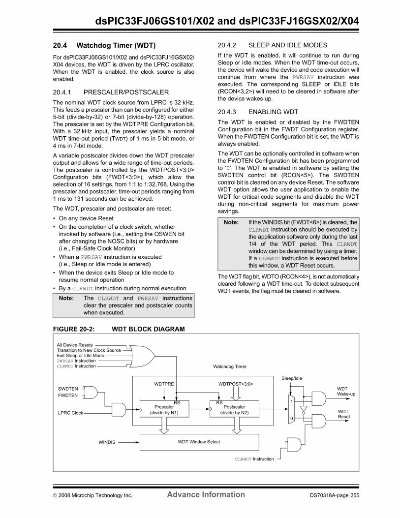
dsPIC33FJ06GS101/X02 and dsPIC33FJ16GSX02/X04
20.4 Watchdog Timer (WDT)For dsPIC33FJ06GS101/X02 and dsPIC33FJ16GSX02/X04 devices, the WDT is driven by the LPRC oscillator.When the WDT is enabled, the clock source is alsoenabled.
20.4.1 PRESCALER/POSTSCALERThe nominal WDT clock source from LPRC is 32 kHz.This feeds a prescaler than can be configured for either5-bit (divide-by-32) or 7-bit (divide-by-128) operation.The prescaler is set by the WDTPRE Configuration bit.With a 32 kHz input, the prescaler yields a nominalWDT time-out period (TWDT) of 1 ms in 5-bit mode, or4 ms in 7-bit mode.
A variable postscaler divides down the WDT prescaleroutput and allows for a wide range of time-out periods.The postscaler is controlled by the WDTPOST<3:0>Configuration bits (FWDT<3:0>), which allow theselection of 16 settings, from 1:1 to 1:32,768. Using theprescaler and postscaler, time-out periods ranging from1 ms to 131 seconds can be achieved.
The WDT, prescaler and postscaler are reset:
• On any device Reset• On the completion of a clock switch, whether
invoked by software (i.e., setting the OSWEN bit after changing the NOSC bits) or by hardware (i.e., Fail-Safe Clock Monitor)
• When a PWRSAV instruction is executed (i.e., Sleep or Idle mode is entered)
• When the device exits Sleep or Idle mode to resume normal operation
• By a CLRWDT instruction during normal execution
20.4.2 SLEEP AND IDLE MODESIf the WDT is enabled, it will continue to run duringSleep or Idle modes. When the WDT time-out occurs,the device will wake the device and code execution willcontinue from where the PWRSAV instruction wasexecuted. The corresponding SLEEP or IDLE bits(RCON<3,2>) will need to be cleared in software afterthe device wakes up.
20.4.3 ENABLING WDTThe WDT is enabled or disabled by the FWDTENConfiguration bit in the FWDT Configuration register.When the FWDTEN Configuration bit is set, the WDT isalways enabled.
The WDT can be optionally controlled in software whenthe FWDTEN Configuration bit has been programmedto ‘0’. The WDT is enabled in software by setting theSWDTEN control bit (RCON<5>). The SWDTENcontrol bit is cleared on any device Reset. The softwareWDT option allows the user application to enable theWDT for critical code segments and disable the WDTduring non-critical segments for maximum powersavings.
The WDT flag bit, WDTO (RCON<4>), is not automaticallycleared following a WDT time-out. To detect subsequentWDT events, the flag must be cleared in software.
FIGURE 20-2: WDT BLOCK DIAGRAM
Note: The CLRWDT and PWRSAV instructionsclear the prescaler and postscaler countswhen executed.
Note: If the WINDIS bit (FWDT<6>) is cleared, theCLRWDT instruction should be executed bythe application software only during the last1/4 of the WDT period. This CLRWDTwindow can be determined by using a timer.If a CLRWDT instruction is executed beforethis window, a WDT Reset occurs.
All Device ResetsTransition to New Clock SourceExit Sleep or Idle ModePWRSAV InstructionCLRWDT Instruction
0
1
WDTPRE WDTPOST<3:0>
Watchdog Timer
Prescaler(divide by N1)
Postscaler(divide by N2)
Sleep/Idle
WDT
WDT Window SelectWINDIS
WDT
CLRWDT Instruction
SWDTENFWDTEN
LPRC Clock
RS RS
Wake-up
Reset
© 2008 Microchip Technology Inc. Advance Information DS70318A-page 255

dsPIC33FJ06GS101/X02 and dsPIC33FJ16GSX02/X04
20.5 JTAG InterfacedsPIC33FJ06GS101/X02 and dsPIC33FJ16GSX02/X04 devices implement a JTAG interface, which sup-ports boundary scan device testing, as well as in-circuitprogramming. Detailed information on this interface willbe provided in future revisions of the document.
20.6 In-Circuit Serial ProgrammingdsPIC33FJ06GS101/X02 and dsPIC33FJ16GSX02/X04 family digital signal controllers can be seriallyprogrammed while in the end application circuit. This isdone with two lines for clock and data and three otherlines for power, ground and the programmingsequence. Serial programming allows customers tomanufacture boards with unprogrammed devices andthen program the digital signal controller just beforeshipping the product. Serial programming also allowsthe most recent firmware or a custom firmware to beprogrammed. Refer to the “dsPIC33F/PIC24H FlashProgramming Specification” (DS70152) for detailsabout In-Circuit Serial Programming (ICSP).
Any of the three pairs of programming clock/data pinscan be used:
• PGC1/EMUC1 and PGD1/EMUD1• PGC2/EMUC2 and PGD2/EMUD2 • PGC3/EMUC3 and PGD3/EMUD3
20.7 In-Circuit DebuggerWhen MPLAB® ICD 2 is selected as a debugger, the in-circuit debugging functionality is enabled. This functionallows simple debugging functions when used withMPLAB IDE. Debugging functionality is controlledthrough the EMUCx (Emulation/Debug Clock) andEMUDx (Emulation/Debug Data) pin functions.
Any of the three pairs of debugging clock/data pins canbe used:
• PGC1/EMUC1 and PGD1/EMUD1• PGC2/EMUC2 and PGD2/EMUD2 • PGC3/EMUC3 and PGD3/EMUD3
To use the in-circuit debugger function of the device,the design must implement ICSP connections toMCLR, VDD, VSS, PGC, PGD and the EMUDx/EMUCxpin pair. In addition, when the feature is enabled, someof the resources are not available for general use.These resources include the first 80 bytes of data RAMand two I/O pins.
DS70318A-page 256 Advance Information © 2008 Microchip Technology Inc.
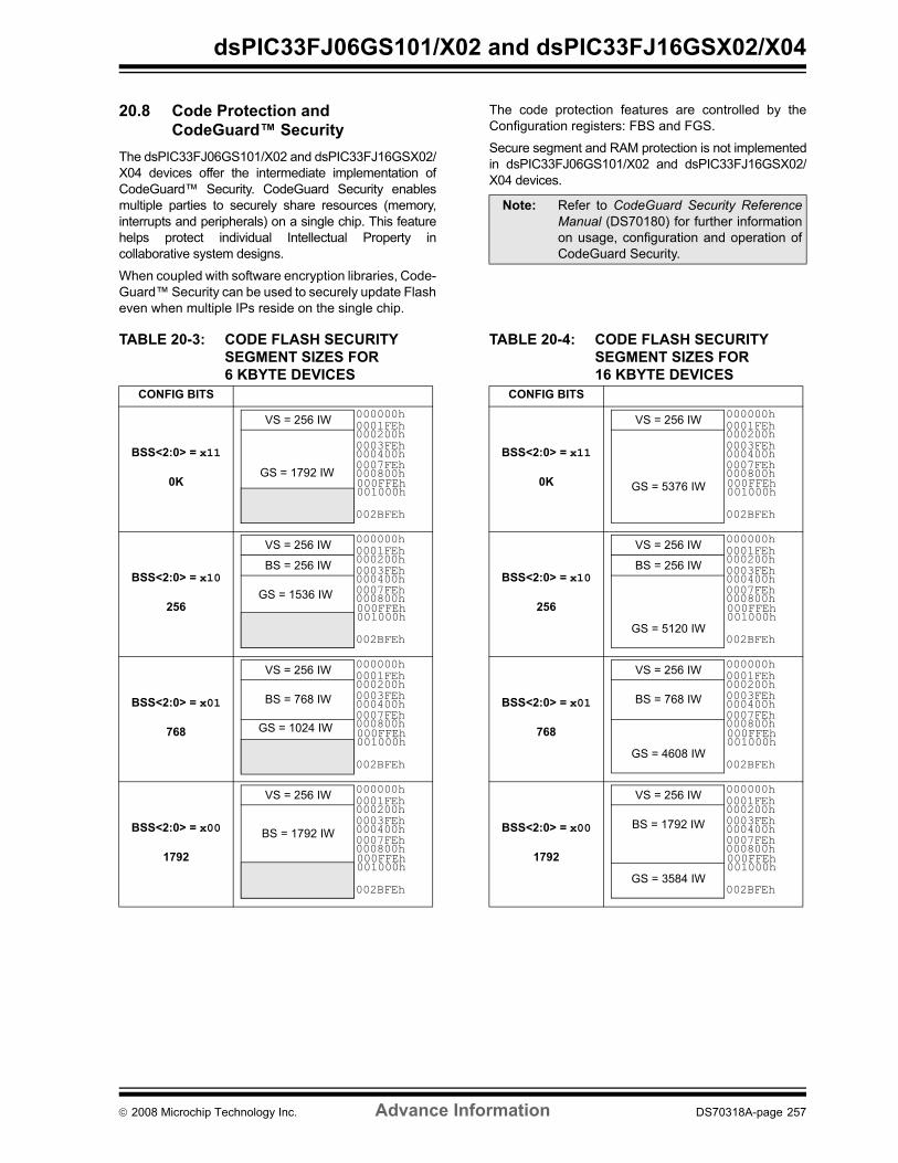
dsPIC33FJ06GS101/X02 and dsPIC33FJ16GSX02/X04
20.8 Code Protection and CodeGuard™ Security
The dsPIC33FJ06GS101/X02 and dsPIC33FJ16GSX02/X04 devices offer the intermediate implementation ofCodeGuard™ Security. CodeGuard Security enablesmultiple parties to securely share resources (memory,interrupts and peripherals) on a single chip. This featurehelps protect individual Intellectual Property incollaborative system designs.
When coupled with software encryption libraries, Code-Guard™ Security can be used to securely update Flasheven when multiple IPs reside on the single chip.
TABLE 20-3: CODE FLASH SECURITY SEGMENT SIZES FOR 6 KBYTE DEVICES
The code protection features are controlled by theConfiguration registers: FBS and FGS.
Secure segment and RAM protection is not implementedin dsPIC33FJ06GS101/X02 and dsPIC33FJ16GSX02/X04 devices.
TABLE 20-4: CODE FLASH SECURITY SEGMENT SIZES FOR 16 KBYTE DEVICES
CONFIG BITS
BSS<2:0> = x11
0K
BSS<2:0> = x10
256
BSS<2:0> = x01
768
BSS<2:0> = x00
1792
002BFEh
0001FEh000200h
000000hVS = 256 IW
0003FEh000400h0007FEh000800hGS = 1792 IW000FFEh001000h
002BFEh
0001FEh000200h
000000hVS = 256 IW
0003FEh000400h0007FEh000800h000FFEh001000h
GS = 1536 IW
BS = 256 IW
002BFEh
0001FEh000200h
000000hVS = 256 IW
0003FEh000400h0007FEh000800h000FFEh001000h
GS = 1024 IW
BS = 768 IW
002BFEh
0001FEh000200h
000000hVS = 256 IW
0003FEh000400h0007FEh000800h000FFEh001000h
BS = 1792 IW
Note: Refer to CodeGuard Security ReferenceManual (DS70180) for further informationon usage, configuration and operation ofCodeGuard Security.
CONFIG BITS
BSS<2:0> = x11
0K
BSS<2:0> = x10
256
BSS<2:0> = x01
768
BSS<2:0> = x00
1792
002BFEh
0001FEh000200h
000000hVS = 256 IW
0003FEh000400h0007FEh000800h
GS = 5376 IW 000FFEh001000h
002BFEh
0001FEh000200h
000000hVS = 256 IW
0003FEh000400h0007FEh000800h000FFEh001000h
GS = 5120 IW
BS = 256 IW
002BFEh
0001FEh000200h
000000hVS = 256 IW
0003FEh000400h0007FEh000800h000FFEh001000h
GS = 4608 IW
BS = 768 IW
002BFEh
0001FEh000200h
000000hVS = 256 IW
0003FEh000400h0007FEh000800h
GS = 3584 IW
000FFEh001000h
BS = 1792 IW
© 2008 Microchip Technology Inc. Advance Information DS70318A-page 257

dsPIC33FJ06GS101/X02 and dsPIC33FJ16GSX02/X04
NOTES:
DS70318A-page 258 Advance Information © 2008 Microchip Technology Inc.

dsPIC33FJ06GS101/X02 and dsPIC33FJ16GSX02/X04
21.0 INSTRUCTION SET SUMMARY
The dsPIC33F instruction set is identical to that of thedsPIC30F.
Most instructions are a single program memory word(24 bits). Only three instructions require two programmemory locations.
Each single-word instruction is a 24-bit word, dividedinto an 8-bit opcode, which specifies the instructiontype and one or more operands, which further specifythe operation of the instruction.
The instruction set is highly orthogonal and is groupedinto five basic categories:
• Word or byte-oriented operations• Bit-oriented operations• Literal operations• DSP operations• Control operations
Table 21-1 shows the general symbols used indescribing the instructions.
The dsPIC33F instruction set summary in Table 21-2lists all the instructions, along with the status flagsaffected by each instruction.
Most word or byte-oriented W register instructions(including barrel shift instructions) have threeoperands:
• The first source operand, which is typically a register ‘Wb’ without any address modifier
• The second source operand, which is typically a register ‘Ws’ with or without an address modifier
• The destination of the result, which is typically a register ‘Wd’ with or without an address modifier
However, word or byte-oriented file register instructionshave two operands:
• The file register specified by the value ‘f’• The destination, which could be either the file
register ‘f’ or the W0 register, which is denoted as ‘WREG’
Most bit-oriented instructions (including simplerotate/shift instructions) have two operands:
• The W register (with or without an address modifier) or file register (specified by the value of ‘Ws’ or ‘f’)
• The bit in the W register or file register (specified by a literal value or indirectly by the contents of register ‘Wb’)
The literal instructions that involve data movement canuse some of the following operands:
• A literal value to be loaded into a W register or file register (specified by ‘k’)
• The W register or file register where the literal value is to be loaded (specified by ‘Wb’ or ‘f’)
However, literal instructions that involve arithmetic orlogical operations use some of the following operands:
• The first source operand, which is a register ‘Wb’ without any address modifier
• The second source operand, which is a literal value
• The destination of the result (only if not the same as the first source operand), which is typically a register ‘Wd’ with or without an address modifier
The MAC class of DSP instructions can use some of thefollowing operands:
• The accumulator (A or B) to be used (required operand)
• The W registers to be used as the two operands• The X and Y address space prefetch operations• The X and Y address space prefetch destinations• The accumulator write-back destination
The other DSP instructions do not involve anymultiplication and can include:
• The accumulator to be used (required)• The source or destination operand (designated as
Wso or Wdo, respectively) with or without an address modifier
• The amount of shift specified by a W register ‘Wn’ or a literal value
The control instructions can use some of the followingoperands:
• A program memory address • The mode of the table read and table write
instructions
Note: This data sheet summarizes the featuresof the dsPIC33FJ06GS101/X02 anddsPIC33FJ16GSX02/X04 devices. It isnot intended to be a comprehensivereference source. To complement theinformation in this data sheet, refer to the“dsPIC33F Family Reference Manual”.Please see the Microchip web site(www.microchip.com) for the latestdsPIC33F Family Reference Manualsections.
© 2008 Microchip Technology Inc. Advance Information DS70318A-page 259

dsPIC33FJ06GS101/X02 and dsPIC33FJ16GSX02/X04
Most instructions are a single word. Certaindouble-word instructions are designed to provide all therequired information in these 48 bits. In the secondword, the 8 MSbs are ‘0’s. If this second word isexecuted as an instruction (by itself), it will execute asa NOP.
The double-word instructions execute in two instructioncycles.
Most single-word instructions are executed in a singleinstruction cycle, unless a conditional test is true, or theprogram counter is changed as a result of theinstruction. In these cases, the execution takes twoinstruction cycles with the additional instruction cycle(s)
executed as a NOP. Notable exceptions are the BRA(unconditional/computed branch), indirect CALL/GOTO,all table reads and writes and RETURN/RETFIEinstructions, which are single-word instructions but taketwo or three cycles. Certain instructions that involveskipping over the subsequent instruction require eithertwo or three cycles if the skip is performed, dependingon whether the instruction being skipped is a single-wordor two-word instruction. Moreover, double-word movesrequire two cycles.
Note: For more details on the instruction set,refer to the “dsPIC30F/33F Programmer’sReference Manual” (DS70157).
TABLE 21-1: SYMBOLS USED IN OPCODE DESCRIPTIONSField Description
#text Means literal defined by “text”(text) Means “content of text”[text] Means “the location addressed by text”{ } Optional field or operation<n:m> Register bit field.b Byte mode selection.d Double-Word mode selection.S Shadow register select.w Word mode selection (default)Acc One of two accumulators {A, B}AWB Accumulator write back destination address register ∈ {W13, [W13]+ = 2}bit4 4-bit bit selection field (used in word addressed instructions) ∈ {0...15}C, DC, N, OV, Z MCU Status bits: Carry, Digit Carry, Negative, Overflow, Sticky ZeroExpr Absolute address, label or expression (resolved by the linker)f File register address ∈ {0x0000...0x1FFF}lit1 1-bit unsigned literal ∈ {0,1}lit4 4-bit unsigned literal ∈ {0...15}lit5 5-bit unsigned literal ∈ {0...31}lit8 8-bit unsigned literal ∈ {0...255}lit10 10-bit unsigned literal ∈ {0...255} for Byte mode, {0:1023} for Word modelit14 14-bit unsigned literal ∈ {0...16384}lit16 16-bit unsigned literal ∈ {0...65535}lit23 23-bit unsigned literal ∈ {0...8388608}; LSb must be ‘0’None Field does not require an entry, can be blankOA, OB, SA, SB DSP Status bits: ACCA Overflow, ACCB Overflow, ACCA Saturate, ACCB SaturatePC Program CounterSlit10 10-bit signed literal ∈ {-512...511}Slit16 16-bit signed literal ∈ {-32768...32767}Slit6 6-bit signed literal ∈ {-16...16}Wb Base W register ∈ {W0..W15}Wd Destination W register ∈ { Wd, [Wd], [Wd++], [Wd--], [++Wd], [--Wd] }Wdo Destination W register ∈
{ Wnd, [Wnd], [Wnd++], [Wnd--], [++Wnd], [--Wnd], [Wnd+Wb] } Wm,Wn Dividend, Divisor working register pair (direct addressing)
DS70318A-page 260 Advance Information © 2008 Microchip Technology Inc.

dsPIC33FJ06GS101/X02 and dsPIC33FJ16GSX02/X04
Wm*Wm Multiplicand and Multiplier working register pair for Square instructions ∈ {W4 * W4,W5 * W5,W6 * W6,W7 * W7}
Wm*Wn Multiplicand and Multiplier working register pair for DSP instructions ∈{W4 * W5,W4 * W6,W4 * W7,W5 * W6,W5 * W7,W6 * W7}
Wn One of 16 working registers ∈ {W0..W15}Wnd One of 16 destination working registers ∈ {W0..W15}Wns One of 16 source working registers ∈ {W0..W15}WREG W0 (working register used in file register instructions)Ws Source W register ∈ { Ws, [Ws], [Ws++], [Ws--], [++Ws], [--Ws] }Wso Source W register ∈
{ Wns, [Wns], [Wns++], [Wns--], [++Wns], [--Wns], [Wns+Wb] } Wx X data space prefetch address register for DSP instructions
∈ {[W8] + = 6, [W8] + = 4, [W8] + = 2, [W8], [W8] - = 6, [W8] - = 4, [W8] - = 2, [W9] + = 6, [W9] + = 4, [W9] + = 2, [W9], [W9] - = 6, [W9] - = 4, [W9] - = 2, [W9 + W12], none}
Wxd X data space prefetch destination register for DSP instructions ∈ {W4..W7}Wy Y data space prefetch address register for DSP instructions
∈ {[W10] + = 6, [W10] + = 4, [W10] + = 2, [W10], [W10] - = 6, [W10] - = 4, [W10] - = 2, [W11] + = 6, [W11] + = 4, [W11] + = 2, [W11], [W11] - = 6, [W11] - = 4, [W11] - = 2, [W11 + W12], none}
Wyd Y data space prefetch destination register for DSP instructions ∈ {W4..W7}
TABLE 21-1: SYMBOLS USED IN OPCODE DESCRIPTIONS (CONTINUED)Field Description
© 2008 Microchip Technology Inc. Advance Information DS70318A-page 261

dsPIC33FJ06GS101/X02 and dsPIC33FJ16GSX02/X04
TABLE 21-2: INSTRUCTION SET OVERVIEW BaseInstr
#AssemblyMnemonic Assembly Syntax Description # of
Words# of
CyclesStatus Flags
Affected
1 ADD ADD Acc Add Accumulators 1 1 OA,OB,SA,SB
ADD f f = f + WREG 1 1 C,DC,N,OV,Z
ADD f,WREG WREG = f + WREG 1 1 C,DC,N,OV,Z
ADD #lit10,Wn Wd = lit10 + Wd 1 1 C,DC,N,OV,Z
ADD Wb,Ws,Wd Wd = Wb + Ws 1 1 C,DC,N,OV,Z
ADD Wb,#lit5,Wd Wd = Wb + lit5 1 1 C,DC,N,OV,Z
ADD Wso,#Slit4,Acc 16-bit Signed Add to Accumulator 1 1 OA,OB,SA,SB
2 ADDC ADDC f f = f + WREG + (C) 1 1 C,DC,N,OV,Z
ADDC f,WREG WREG = f + WREG + (C) 1 1 C,DC,N,OV,Z
ADDC #lit10,Wn Wd = lit10 + Wd + (C) 1 1 C,DC,N,OV,Z
ADDC Wb,Ws,Wd Wd = Wb + Ws + (C) 1 1 C,DC,N,OV,Z
ADDC Wb,#lit5,Wd Wd = Wb + lit5 + (C) 1 1 C,DC,N,OV,Z
3 AND AND f f = f .AND. WREG 1 1 N,Z
AND f,WREG WREG = f .AND. WREG 1 1 N,Z
AND #lit10,Wn Wd = lit10 .AND. Wd 1 1 N,Z
AND Wb,Ws,Wd Wd = Wb .AND. Ws 1 1 N,Z
AND Wb,#lit5,Wd Wd = Wb .AND. lit5 1 1 N,Z
4 ASR ASR f f = Arithmetic Right Shift f 1 1 C,N,OV,Z
ASR f,WREG WREG = Arithmetic Right Shift f 1 1 C,N,OV,Z
ASR Ws,Wd Wd = Arithmetic Right Shift Ws 1 1 C,N,OV,Z
ASR Wb,Wns,Wnd Wnd = Arithmetic Right Shift Wb by Wns 1 1 N,Z
ASR Wb,#lit5,Wnd Wnd = Arithmetic Right Shift Wb by lit5 1 1 N,Z
5 BCLR BCLR f,#bit4 Bit Clear f 1 1 None
BCLR Ws,#bit4 Bit Clear Ws 1 1 None
6 BRA BRA C,Expr Branch if Carry 1 1 (2) None
BRA GE,Expr Branch if greater than or equal 1 1 (2) None
BRA GEU,Expr Branch if unsigned greater than or equal 1 1 (2) None
BRA GT,Expr Branch if greater than 1 1 (2) None
BRA GTU,Expr Branch if unsigned greater than 1 1 (2) None
BRA LE,Expr Branch if less than or equal 1 1 (2) None
BRA LEU,Expr Branch if unsigned less than or equal 1 1 (2) None
BRA LT,Expr Branch if less than 1 1 (2) None
BRA LTU,Expr Branch if unsigned less than 1 1 (2) None
BRA N,Expr Branch if Negative 1 1 (2) None
BRA NC,Expr Branch if Not Carry 1 1 (2) None
BRA NN,Expr Branch if Not Negative 1 1 (2) None
BRA NOV,Expr Branch if Not Overflow 1 1 (2) None
BRA NZ,Expr Branch if Not Zero 1 1 (2) None
BRA OA,Expr Branch if Accumulator A overflow 1 1 (2) None
BRA OB,Expr Branch if Accumulator B overflow 1 1 (2) None
BRA OV,Expr Branch if Overflow 1 1 (2) None
BRA SA,Expr Branch if Accumulator A saturated 1 1 (2) None
BRA SB,Expr Branch if Accumulator B saturated 1 1 (2) None
BRA Expr Branch Unconditionally 1 2 None
BRA Z,Expr Branch if Zero 1 1 (2) None
BRA Wn Computed Branch 1 2 None
7 BSET BSET f,#bit4 Bit Set f 1 1 None
BSET Ws,#bit4 Bit Set Ws 1 1 None
8 BSW BSW.C Ws,Wb Write C bit to Ws<Wb> 1 1 None
BSW.Z Ws,Wb Write Z bit to Ws<Wb> 1 1 None
9 BTG BTG f,#bit4 Bit Toggle f 1 1 None
BTG Ws,#bit4 Bit Toggle Ws 1 1 None
DS70318A-page 262 Advance Information © 2008 Microchip Technology Inc.

dsPIC33FJ06GS101/X02 and dsPIC33FJ16GSX02/X04
10 BTSC BTSC f,#bit4 Bit Test f, Skip if Clear 1 1 (2 or 3)
None
BTSC Ws,#bit4 Bit Test Ws, Skip if Clear 1 1 (2 or 3)
None
11 BTSS BTSS f,#bit4 Bit Test f, Skip if Set 1 1 (2 or 3)
None
BTSS Ws,#bit4 Bit Test Ws, Skip if Set 1 1 (2 or 3)
None
12 BTST BTST f,#bit4 Bit Test f 1 1 Z
BTST.C Ws,#bit4 Bit Test Ws to C 1 1 C
BTST.Z Ws,#bit4 Bit Test Ws to Z 1 1 Z
BTST.C Ws,Wb Bit Test Ws<Wb> to C 1 1 C
BTST.Z Ws,Wb Bit Test Ws<Wb> to Z 1 1 Z
13 BTSTS BTSTS f,#bit4 Bit Test then Set f 1 1 Z
BTSTS.C Ws,#bit4 Bit Test Ws to C, then Set 1 1 C
BTSTS.Z Ws,#bit4 Bit Test Ws to Z, then Set 1 1 Z
14 CALL CALL lit23 Call subroutine 2 2 None
CALL Wn Call indirect subroutine 1 2 None
15 CLR CLR f f = 0x0000 1 1 None
CLR WREG WREG = 0x0000 1 1 None
CLR Ws Ws = 0x0000 1 1 None
CLR Acc,Wx,Wxd,Wy,Wyd,AWB Clear Accumulator 1 1 OA,OB,SA,SB
16 CLRWDT CLRWDT Clear Watchdog Timer 1 1 WDTO,Sleep
17 COM COM f f = f 1 1 N,Z
COM f,WREG WREG = f 1 1 N,Z
COM Ws,Wd Wd = Ws 1 1 N,Z
18 CP CP f Compare f with WREG 1 1 C,DC,N,OV,Z
CP Wb,#lit5 Compare Wb with lit5 1 1 C,DC,N,OV,Z
CP Wb,Ws Compare Wb with Ws (Wb – Ws) 1 1 C,DC,N,OV,Z
19 CP0 CP0 f Compare f with 0x0000 1 1 C,DC,N,OV,Z
CP0 Ws Compare Ws with 0x0000 1 1 C,DC,N,OV,Z
20 CPB CPB f Compare f with WREG, with Borrow 1 1 C,DC,N,OV,Z
CPB Wb,#lit5 Compare Wb with lit5, with Borrow 1 1 C,DC,N,OV,Z
CPB Wb,Ws Compare Wb with Ws, with Borrow (Wb – Ws – C)
1 1 C,DC,N,OV,Z
21 CPSEQ CPSEQ Wb, Wn Compare Wb with Wn, skip if = 1 1 (2 or 3)
None
22 CPSGT CPSGT Wb, Wn Compare Wb with Wn, skip if > 1 1 (2 or 3)
None
23 CPSLT CPSLT Wb, Wn Compare Wb with Wn, skip if < 1 1 (2 or 3)
None
24 CPSNE CPSNE Wb, Wn Compare Wb with Wn, skip if ≠ 1 1 (2 or 3)
None
25 DAW DAW Wn Wn = decimal adjust Wn 1 1 C
26 DEC DEC f f = f – 1 1 1 C,DC,N,OV,Z
DEC f,WREG WREG = f – 1 1 1 C,DC,N,OV,Z
DEC Ws,Wd Wd = Ws – 1 1 1 C,DC,N,OV,Z
27 DEC2 DEC2 f f = f – 2 1 1 C,DC,N,OV,Z
DEC2 f,WREG WREG = f – 2 1 1 C,DC,N,OV,Z
DEC2 Ws,Wd Wd = Ws – 2 1 1 C,DC,N,OV,Z
28 DISI DISI #lit14 Disable Interrupts for k instruction cycles 1 1 None
TABLE 21-2: INSTRUCTION SET OVERVIEW (CONTINUED) BaseInstr
#AssemblyMnemonic Assembly Syntax Description # of
Words# of
CyclesStatus Flags
Affected
© 2008 Microchip Technology Inc. Advance Information DS70318A-page 263

dsPIC33FJ06GS101/X02 and dsPIC33FJ16GSX02/X04
29 DIV DIV.S Wm,Wn Signed 16/16-bit Integer Divide 1 18 N,Z,C,OV
DIV.SD Wm,Wn Signed 32/16-bit Integer Divide 1 18 N,Z,C,OV
DIV.U Wm,Wn Unsigned 16/16-bit Integer Divide 1 18 N,Z,C,OV
DIV.UD Wm,Wn Unsigned 32/16-bit Integer Divide 1 18 N,Z,C,OV
30 DIVF DIVF Wm,Wn Signed 16/16-bit Fractional Divide 1 18 N,Z,C,OV
31 DO DO #lit14,Expr Do code to PC + Expr, lit14 + 1 times 2 2 None
DO Wn,Expr Do code to PC + Expr, (Wn) + 1 times 2 2 None
32 ED ED Wm*Wm,Acc,Wx,Wy,Wxd Euclidean Distance (no accumulate) 1 1 OA,OB,OAB,SA,SB,SAB
33 EDAC EDAC Wm*Wm,Acc,Wx,Wy,Wxd Euclidean Distance 1 1 OA,OB,OAB,SA,SB,SAB
34 EXCH EXCH Wns,Wnd Swap Wns with Wnd 1 1 None
35 FBCL FBCL Ws,Wnd Find Bit Change from Left (MSb) Side 1 1 C
36 FF1L FF1L Ws,Wnd Find First One from Left (MSb) Side 1 1 C
37 FF1R FF1R Ws,Wnd Find First One from Right (LSb) Side 1 1 C
38 GOTO GOTO Expr Go to address 2 2 None
GOTO Wn Go to indirect 1 2 None
39 INC INC f f = f + 1 1 1 C,DC,N,OV,Z
INC f,WREG WREG = f + 1 1 1 C,DC,N,OV,Z
INC Ws,Wd Wd = Ws + 1 1 1 C,DC,N,OV,Z
40 INC2 INC2 f f = f + 2 1 1 C,DC,N,OV,Z
INC2 f,WREG WREG = f + 2 1 1 C,DC,N,OV,Z
INC2 Ws,Wd Wd = Ws + 2 1 1 C,DC,N,OV,Z
41 IOR IOR f f = f .IOR. WREG 1 1 N,Z
IOR f,WREG WREG = f .IOR. WREG 1 1 N,Z
IOR #lit10,Wn Wd = lit10 .IOR. Wd 1 1 N,Z
IOR Wb,Ws,Wd Wd = Wb .IOR. Ws 1 1 N,Z
IOR Wb,#lit5,Wd Wd = Wb .IOR. lit5 1 1 N,Z
42 LAC LAC Wso,#Slit4,Acc Load Accumulator 1 1 OA,OB,OAB,SA,SB,SAB
43 LNK LNK #lit14 Link Frame Pointer 1 1 None
44 LSR LSR f f = Logical Right Shift f 1 1 C,N,OV,Z
LSR f,WREG WREG = Logical Right Shift f 1 1 C,N,OV,Z
LSR Ws,Wd Wd = Logical Right Shift Ws 1 1 C,N,OV,Z
LSR Wb,Wns,Wnd Wnd = Logical Right Shift Wb by Wns 1 1 N,Z
LSR Wb,#lit5,Wnd Wnd = Logical Right Shift Wb by lit5 1 1 N,Z
45 MAC MAC Wm*Wn,Acc,Wx,Wxd,Wy,Wyd,AWB
Multiply and Accumulate 1 1 OA,OB,OAB,SA,SB,SAB
MAC Wm*Wm,Acc,Wx,Wxd,Wy,Wyd Square and Accumulate 1 1 OA,OB,OAB,SA,SB,SAB
46 MOV MOV f,Wn Move f to Wn 1 1 None
MOV f Move f to f 1 1 N,Z
MOV f,WREG Move f to WREG 1 1 N,Z
MOV #lit16,Wn Move 16-bit literal to Wn 1 1 None
MOV.b #lit8,Wn Move 8-bit literal to Wn 1 1 None
MOV Wn,f Move Wn to f 1 1 None
MOV Wso,Wdo Move Ws to Wd 1 1 None
MOV WREG,f Move WREG to f 1 1 N,Z
MOV.D Wns,Wd Move Double from W(ns):W(ns + 1) to Wd 1 2 None
MOV.D Ws,Wnd Move Double from Ws to W(nd + 1):W(nd) 1 2 None
47 MOVSAC MOVSAC Acc,Wx,Wxd,Wy,Wyd,AWB Prefetch and store accumulator 1 1 None
TABLE 21-2: INSTRUCTION SET OVERVIEW (CONTINUED) BaseInstr
#AssemblyMnemonic Assembly Syntax Description # of
Words# of
CyclesStatus Flags
Affected
DS70318A-page 264 Advance Information © 2008 Microchip Technology Inc.
dsPIC33FJ06GS101/X02 and dsPIC33FJ16GSX02/X04
48 MPY MPY Wm*Wn,Acc,Wx,Wxd,Wy,Wyd
Multiply Wm by Wn to Accumulator 1 1 OA,OB,OAB,SA,SB,SAB
MPY Wm*Wm,Acc,Wx,Wxd,Wy,Wyd
Square Wm to Accumulator 1 1 OA,OB,OAB,SA,SB,SAB
49 MPY.N MPY.N Wm*Wn,Acc,Wx,Wxd,Wy,Wyd
-(Multiply Wm by Wn) to Accumulator 1 1 None
50 MSC MSC Wm*Wm,Acc,Wx,Wxd,Wy,Wyd,AWB
Multiply and Subtract from Accumulator 1 1 OA,OB,OAB,SA,SB,SAB
51 MUL MUL.SS Wb,Ws,Wnd {Wnd + 1, Wnd} = signed(Wb) * signed(Ws) 1 1 None
MUL.SU Wb,Ws,Wnd {Wnd + 1, Wnd} = signed(Wb) * unsigned(Ws) 1 1 None
MUL.US Wb,Ws,Wnd {Wnd + 1, Wnd} = unsigned(Wb) * signed(Ws) 1 1 None
MUL.UU Wb,Ws,Wnd {Wnd + 1, Wnd} = unsigned(Wb) * unsigned(Ws)
1 1 None
MUL.SU Wb,#lit5,Wnd {Wnd + 1, Wnd} = signed(Wb) * unsigned(lit5) 1 1 None
MUL.UU Wb,#lit5,Wnd {Wnd + 1, Wnd} = unsigned(Wb) * unsigned(lit5)
1 1 None
MUL f W3:W2 = f * WREG 1 1 None
52 NEG NEG Acc Negate Accumulator 1 1 OA,OB,OAB,SA,SB,SAB
NEG f f = f + 1 1 1 C,DC,N,OV,Z
NEG f,WREG WREG = f + 1 1 1 C,DC,N,OV,Z
NEG Ws,Wd Wd = Ws + 1 1 1 C,DC,N,OV,Z
53 NOP NOP No Operation 1 1 None
NOPR No Operation 1 1 None
54 POP POP f Pop f from Top-of-Stack (TOS) 1 1 None
POP Wdo Pop from Top-of-Stack (TOS) to Wdo 1 1 None
POP.D Wnd Pop from Top-of-Stack (TOS) to W(nd):W(nd + 1)
1 2 None
POP.S Pop Shadow Registers 1 1 All
55 PUSH PUSH f Push f to Top-of-Stack (TOS) 1 1 None
PUSH Wso Push Wso to Top-of-Stack (TOS) 1 1 None
PUSH.D Wns Push W(ns):W(ns + 1) to Top-of-Stack (TOS) 1 2 None
PUSH.S Push Shadow Registers 1 1 None
56 PWRSAV PWRSAV #lit1 Go into Sleep or Idle mode 1 1 WDTO,Sleep
57 RCALL RCALL Expr Relative Call 1 2 None
RCALL Wn Computed Call 1 2 None
58 REPEAT REPEAT #lit14 Repeat Next Instruction lit14 + 1 times 1 1 None
REPEAT Wn Repeat Next Instruction (Wn) + 1 times 1 1 None
59 RESET RESET Software device Reset 1 1 None
60 RETFIE RETFIE Return from interrupt 1 3 (2) None
61 RETLW RETLW #lit10,Wn Return with literal in Wn 1 3 (2) None
62 RETURN RETURN Return from Subroutine 1 3 (2) None
63 RLC RLC f f = Rotate Left through Carry f 1 1 C,N,Z
RLC f,WREG WREG = Rotate Left through Carry f 1 1 C,N,Z
RLC Ws,Wd Wd = Rotate Left through Carry Ws 1 1 C,N,Z
64 RLNC RLNC f f = Rotate Left (No Carry) f 1 1 N,Z
RLNC f,WREG WREG = Rotate Left (No Carry) f 1 1 N,Z
RLNC Ws,Wd Wd = Rotate Left (No Carry) Ws 1 1 N,Z
65 RRC RRC f f = Rotate Right through Carry f 1 1 C,N,Z
RRC f,WREG WREG = Rotate Right through Carry f 1 1 C,N,Z
RRC Ws,Wd Wd = Rotate Right through Carry Ws 1 1 C,N,Z
TABLE 21-2: INSTRUCTION SET OVERVIEW (CONTINUED) BaseInstr
#AssemblyMnemonic Assembly Syntax Description # of
Words# of
CyclesStatus Flags
Affected
© 2008 Microchip Technology Inc. Advance Information DS70318A-page 265
dsPIC33FJ06GS101/X02 and dsPIC33FJ16GSX02/X04
66 RRNC RRNC f f = Rotate Right (No Carry) f 1 1 N,Z
RRNC f,WREG WREG = Rotate Right (No Carry) f 1 1 N,Z
RRNC Ws,Wd Wd = Rotate Right (No Carry) Ws 1 1 N,Z
67 SAC SAC Acc,#Slit4,Wdo Store Accumulator 1 1 None
SAC.R Acc,#Slit4,Wdo Store Rounded Accumulator 1 1 None
68 SE SE Ws,Wnd Wnd = sign-extended Ws 1 1 C,N,Z
69 SETM SETM f f = 0xFFFF 1 1 None
SETM WREG WREG = 0xFFFF 1 1 None
SETM Ws Ws = 0xFFFF 1 1 None
70 SFTAC SFTAC Acc,Wn Arithmetic Shift Accumulator by (Wn) 1 1 OA,OB,OAB,SA,SB,SAB
SFTAC Acc,#Slit6 Arithmetic Shift Accumulator by Slit6 1 1 OA,OB,OAB,SA,SB,SAB
71 SL SL f f = Left Shift f 1 1 C,N,OV,Z
SL f,WREG WREG = Left Shift f 1 1 C,N,OV,Z
SL Ws,Wd Wd = Left Shift Ws 1 1 C,N,OV,Z
SL Wb,Wns,Wnd Wnd = Left Shift Wb by Wns 1 1 N,Z
SL Wb,#lit5,Wnd Wnd = Left Shift Wb by lit5 1 1 N,Z
72 SUB SUB Acc Subtract Accumulators 1 1 OA,OB,OAB,SA,SB,SAB
SUB f f = f – WREG 1 1 C,DC,N,OV,Z
SUB f,WREG WREG = f – WREG 1 1 C,DC,N,OV,Z
SUB #lit10,Wn Wn = Wn – lit10 1 1 C,DC,N,OV,Z
SUB Wb,Ws,Wd Wd = Wb – Ws 1 1 C,DC,N,OV,Z
SUB Wb,#lit5,Wd Wd = Wb – lit5 1 1 C,DC,N,OV,Z
73 SUBB SUBB f f = f – WREG – (C) 1 1 C,DC,N,OV,Z
SUBB f,WREG WREG = f – WREG – (C) 1 1 C,DC,N,OV,Z
SUBB #lit10,Wn Wn = Wn – lit10 – (C) 1 1 C,DC,N,OV,Z
SUBB Wb,Ws,Wd Wd = Wb – Ws – (C) 1 1 C,DC,N,OV,Z
SUBB Wb,#lit5,Wd Wd = Wb – lit5 – (C) 1 1 C,DC,N,OV,Z
74 SUBR SUBR f f = WREG – f 1 1 C,DC,N,OV,Z
SUBR f,WREG WREG = WREG – f 1 1 C,DC,N,OV,Z
SUBR Wb,Ws,Wd Wd = Ws – Wb 1 1 C,DC,N,OV,Z
SUBR Wb,#lit5,Wd Wd = lit5 – Wb 1 1 C,DC,N,OV,Z
75 SUBBR SUBBR f f = WREG – f – (C) 1 1 C,DC,N,OV,Z
SUBBR f,WREG WREG = WREG – f – (C) 1 1 C,DC,N,OV,Z
SUBBR Wb,Ws,Wd Wd = Ws – Wb – (C) 1 1 C,DC,N,OV,Z
SUBBR Wb,#lit5,Wd Wd = lit5 – Wb – (C) 1 1 C,DC,N,OV,Z
76 SWAP SWAP.b Wn Wn = nibble swap Wn 1 1 None
SWAP Wn Wn = byte swap Wn 1 1 None
77 TBLRDH TBLRDH Ws,Wd Read Prog<23:16> to Wd<7:0> 1 2 None
78 TBLRDL TBLRDL Ws,Wd Read Prog<15:0> to Wd 1 2 None
79 TBLWTH TBLWTH Ws,Wd Write Ws<7:0> to Prog<23:16> 1 2 None
80 TBLWTL TBLWTL Ws,Wd Write Ws to Prog<15:0> 1 2 None
81 ULNK ULNK Unlink Frame Pointer 1 1 None
82 XOR XOR f f = f .XOR. WREG 1 1 N,Z
XOR f,WREG WREG = f .XOR. WREG 1 1 N,Z
XOR #lit10,Wn Wd = lit10 .XOR. Wd 1 1 N,Z
XOR Wb,Ws,Wd Wd = Wb .XOR. Ws 1 1 N,Z
XOR Wb,#lit5,Wd Wd = Wb .XOR. lit5 1 1 N,Z
83 ZE ZE Ws,Wnd Wnd = Zero-extend Ws 1 1 C,Z,N
TABLE 21-2: INSTRUCTION SET OVERVIEW (CONTINUED) BaseInstr
#AssemblyMnemonic Assembly Syntax Description # of
Words# of
CyclesStatus Flags
Affected
DS70318A-page 266 Advance Information © 2008 Microchip Technology Inc.
dsPIC33FJ06GS101/X02 and dsPIC33FJ16GSX02/X04
22.0 DEVELOPMENT SUPPORTThe PIC® microcontrollers are supported with a fullrange of hardware and software development tools:
• Integrated Development Environment- MPLAB® IDE Software
• Assemblers/Compilers/Linkers- MPASMTM Assembler- MPLAB C18 and MPLAB C30 C Compilers- MPLINKTM Object Linker/
MPLIBTM Object Librarian- MPLAB ASM30 Assembler/Linker/Library
• Simulators- MPLAB SIM Software Simulator
• Emulators- MPLAB ICE 2000 In-Circuit Emulator- MPLAB REAL ICE™ In-Circuit Emulator
• In-Circuit Debugger- MPLAB ICD 2
• Device Programmers- PICSTART® Plus Development Programmer- MPLAB PM3 Device Programmer- PICkit™ 2 Development Programmer
• Low-Cost Demonstration and Development Boards and Evaluation Kits
22.1 MPLAB Integrated Development Environment Software
The MPLAB IDE software brings an ease of softwaredevelopment previously unseen in the 8/16-bitmicrocontroller market. The MPLAB IDE is a Windows®
operating system-based application that contains:
• A single graphical interface to all debugging tools- Simulator- Programmer (sold separately)- Emulator (sold separately)- In-Circuit Debugger (sold separately)
• A full-featured editor with color-coded context• A multiple project manager• Customizable data windows with direct edit of
contents• High-level source code debugging• Visual device initializer for easy register
initialization• Mouse over variable inspection• Drag and drop variables from source to watch
windows• Extensive on-line help• Integration of select third party tools, such as
HI-TECH Software C Compilers and IAR C Compilers
The MPLAB IDE allows you to:
• Edit your source files (either assembly or C)• One touch assemble (or compile) and download
to PIC MCU emulator and simulator tools (automatically updates all project information)
• Debug using:- Source files (assembly or C)- Mixed assembly and C- Machine code
MPLAB IDE supports multiple debugging tools in asingle development paradigm, from the cost-effectivesimulators, through low-cost in-circuit debuggers, tofull-featured emulators. This eliminates the learningcurve when upgrading to tools with increased flexibilityand power.
© 2008 Microchip Technology Inc. Advance Information DS70318A-page 267

dsPIC33FJ06GS101/X02 and dsPIC33FJ16GSX02/X04
22.2 MPASM AssemblerThe MPASM Assembler is a full-featured, universalmacro assembler for all PIC MCUs.
The MPASM Assembler generates relocatable objectfiles for the MPLINK Object Linker, Intel® standard HEXfiles, MAP files to detail memory usage and symbolreference, absolute LST files that contain source linesand generated machine code and COFF files fordebugging.
The MPASM Assembler features include:
• Integration into MPLAB IDE projects• User-defined macros to streamline
assembly code• Conditional assembly for multi-purpose
source files• Directives that allow complete control over the
assembly process
22.3 MPLAB C18 and MPLAB C30 C Compilers
The MPLAB C18 and MPLAB C30 Code DevelopmentSystems are complete ANSI C compilers forMicrochip’s PIC18 and PIC24 families of microcontrol-lers and the dsPIC30 and dsPIC33 family of digital sig-nal controllers. These compilers provide powerfulintegration capabilities, superior code optimization andease of use not found with other compilers.
For easy source level debugging, the compilers providesymbol information that is optimized to the MPLAB IDEdebugger.
22.4 MPLINK Object Linker/MPLIB Object Librarian
The MPLINK Object Linker combines relocatableobjects created by the MPASM Assembler and theMPLAB C18 C Compiler. It can link relocatable objectsfrom precompiled libraries, using directives from alinker script.
The MPLIB Object Librarian manages the creation andmodification of library files of precompiled code. Whena routine from a library is called from a source file, onlythe modules that contain that routine will be linked inwith the application. This allows large libraries to beused efficiently in many different applications.
The object linker/library features include:
• Efficient linking of single libraries instead of linking many smaller files
• Enhanced code maintainability by grouping related modules together
• Flexible creation of libraries with easy module listing, replacement, deletion and extraction
22.5 MPLAB ASM30 Assembler, Linker and Librarian
MPLAB ASM30 Assembler produces relocatablemachine code from symbolic assembly language fordsPIC30F devices. MPLAB C30 C Compiler uses theassembler to produce its object file. The assemblergenerates relocatable object files that can then bearchived or linked with other relocatable object files andarchives to create an executable file. Notable featuresof the assembler include:
• Support for the entire dsPIC30F instruction set• Support for fixed-point and floating-point data• Command line interface• Rich directive set• Flexible macro language• MPLAB IDE compatibility
22.6 MPLAB SIM Software SimulatorThe MPLAB SIM Software Simulator allows codedevelopment in a PC-hosted environment bysimulating the PIC MCUs and dsPIC® DSCs on aninstruction level. On any given instruction, the dataareas can be examined or modified and stimuli can beapplied from a comprehensive stimulus controller.Registers can be logged to files for further run-timeanalysis. The trace buffer and logic analyzer displayextend the power of the simulator to record and trackprogram execution, actions on I/O, most peripheralsand internal registers.
The MPLAB SIM Software Simulator fully supportssymbolic debugging using the MPLAB C18 andMPLAB C30 C Compilers, and the MPASM andMPLAB ASM30 Assemblers. The software simulatoroffers the flexibility to develop and debug code outsideof the hardware laboratory environment, making it anexcellent, economical software development tool.
DS70318A-page 268 Advance Information © 2008 Microchip Technology Inc.

dsPIC33FJ06GS101/X02 and dsPIC33FJ16GSX02/X04
22.7 MPLAB ICE 2000 High-Performance In-Circuit Emulator
The MPLAB ICE 2000 In-Circuit Emulator is intendedto provide the product development engineer with acomplete microcontroller design tool set for PICmicrocontrollers. Software control of the MPLAB ICE2000 In-Circuit Emulator is advanced by the MPLABIntegrated Development Environment, which allowsediting, building, downloading and source debuggingfrom a single environment.
The MPLAB ICE 2000 is a full-featured emulatorsystem with enhanced trace, trigger and datamonitoring features. Interchangeable processormodules allow the system to be easily reconfigured foremulation of different processors. The architecture ofthe MPLAB ICE 2000 In-Circuit Emulator allowsexpansion to support new PIC microcontrollers.
The MPLAB ICE 2000 In-Circuit Emulator system hasbeen designed as a real-time emulation system withadvanced features that are typically found on moreexpensive development tools. The PC platform andMicrosoft® Windows® 32-bit operating system werechosen to best make these features available in asimple, unified application.
22.8 MPLAB REAL ICE In-Circuit Emulator System
MPLAB REAL ICE In-Circuit Emulator System isMicrochip’s next generation high-speed emulator forMicrochip Flash DSC and MCU devices. It debugs andprograms PIC® Flash MCUs and dsPIC® Flash DSCswith the easy-to-use, powerful graphical user interface ofthe MPLAB Integrated Development Environment (IDE),included with each kit.
The MPLAB REAL ICE probe is connected to the designengineer’s PC using a high-speed USB 2.0 interface andis connected to the target with either a connectorcompatible with the popular MPLAB ICD 2 system(RJ11) or with the new high-speed, noise tolerant,Low-Voltage Differential Signal (LVDS) interconnection(CAT5).
MPLAB REAL ICE is field upgradeable through futurefirmware downloads in MPLAB IDE. In upcomingreleases of MPLAB IDE, new devices will be supported,and new features will be added, such as software break-points and assembly code trace. MPLAB REAL ICEoffers significant advantages over competitive emulatorsincluding low-cost, full-speed emulation, real-timevariable watches, trace analysis, complex breakpoints, aruggedized probe interface and long (up to three meters)interconnection cables.
22.9 MPLAB ICD 2 In-Circuit DebuggerMicrochip’s In-Circuit Debugger, MPLAB ICD 2, is apowerful, low-cost, run-time development tool,connecting to the host PC via an RS-232 or high-speedUSB interface. This tool is based on the Flash PICMCUs and can be used to develop for these and otherPIC MCUs and dsPIC DSCs. The MPLAB ICD 2 utilizesthe in-circuit debugging capability built into the Flashdevices. This feature, along with Microchip’s In-CircuitSerial ProgrammingTM (ICSPTM) protocol, offerscost-effective, in-circuit Flash debugging from thegraphical user interface of the MPLAB IntegratedDevelopment Environment. This enables a designer todevelop and debug source code by setting breakpoints,single stepping and watching variables, and CPUstatus and peripheral registers. Running at full speedenables testing hardware and applications in realtime. MPLAB ICD 2 also serves as a developmentprogrammer for selected PIC devices.
22.10 MPLAB PM3 Device ProgrammerThe MPLAB PM3 Device Programmer is a universal,CE compliant device programmer with programmablevoltage verification at VDDMIN and VDDMAX formaximum reliability. It features a large LCD display(128 x 64) for menus and error messages and amodular, detachable socket assembly to supportvarious package types. The ICSP™ cable assembly isincluded as a standard item. In Stand-Alone mode, theMPLAB PM3 Device Programmer can read, verify andprogram PIC devices without a PC connection. It canalso set code protection in this mode. The MPLAB PM3connects to the host PC via an RS-232 or USB cable.The MPLAB PM3 has high-speed communications andoptimized algorithms for quick programming of largememory devices and incorporates an SD/MMC card forfile storage and secure data applications.
© 2008 Microchip Technology Inc. Advance Information DS70318A-page 269

dsPIC33FJ06GS101/X02 and dsPIC33FJ16GSX02/X04
22.11 PICSTART Plus Development Programmer
The PICSTART Plus Development Programmer is aneasy-to-use, low-cost, prototype programmer. Itconnects to the PC via a COM (RS-232) port. MPLABIntegrated Development Environment software makesusing the programmer simple and efficient. ThePICSTART Plus Development Programmer supportsmost PIC devices in DIP packages up to 40 pins.Larger pin count devices, such as the PIC16C92X andPIC17C76X, may be supported with an adapter socket.The PICSTART Plus Development Programmer is CEcompliant.
22.12 PICkit 2 Development ProgrammerThe PICkit™ 2 Development Programmer is a low-costprogrammer and selected Flash device debugger withan easy-to-use interface for programming many ofMicrochip’s baseline, mid-range and PIC18F families ofFlash memory microcontrollers. The PICkit 2 Starter Kitincludes a prototyping development board, twelvesequential lessons, software and HI-TECH’s PICC™Lite C compiler, and is designed to help get up to speedquickly using PIC® microcontrollers. The kit provideseverything needed to program, evaluate and developapplications using Microchip’s powerful, mid-rangeFlash memory family of microcontrollers.
22.13 Demonstration, Development and Evaluation Boards
A wide variety of demonstration, development andevaluation boards for various PIC MCUs and dsPICDSCs allows quick application development on fullyfunctional systems. Most boards include prototypingareas for adding custom circuitry and provide applicationfirmware and source code for examination and modifica-tion.
The boards support a variety of features, including LEDs,temperature sensors, switches, speakers, RS-232interfaces, LCD displays, potentiometers and additionalEEPROM memory.
The demonstration and development boards can beused in teaching environments, for prototyping customcircuits and for learning about various microcontrollerapplications.
In addition to the PICDEM™ and dsPICDEM™demonstration/development board series of circuits,Microchip has a line of evaluation kits and demonstra-tion software for analog filter design, KEELOQ® securityICs, CAN, IrDA®, PowerSmart battery management,SEEVAL® evaluation system, Sigma-Delta ADC, flowrate sensing, plus many more.
Check the Microchip web page (www.microchip.com)for the complete list of demonstration, developmentand evaluation kits.
DS70318A-page 270 Advance Information © 2008 Microchip Technology Inc.

dsPIC33FJ06GS101/X02 and dsPIC33FJ16GSX02/X04
23.0 ELECTRICAL CHARACTERISTICSThis section provides an overview of dsPIC33FJ06GS101/X02 and dsPIC33FJ16GSX02/X04 electrical characteristics.Additional information will be provided in future revisions of this document as it becomes available.
Absolute maximum ratings for the dsPIC33FJ06GS101/X02 and dsPIC33FJ16GSX02/X04 family are listed below.Exposure to these maximum rating conditions for extended periods may affect device reliability. Functional operation ofthe device at these or any other conditions above the parameters indicated in the operation listings of this specificationis not implied.
Absolute Maximum Ratings(1) Ambient temperature under bias............................................................................................................ .-40°C to +125°CStorage temperature .............................................................................................................................. -65°C to +150°CVoltage on VDD with respect to VSS ......................................................................................................... -0.3V to +4.0VVoltage on any combined analog and digital pin and MCLR, with respect to VSS ......................... -0.3V to (VDD + 0.3V)Voltage on any digital-only pin with respect to VSS .................................................................................. -0.3V to +5.6VVoltage on VDDCORE with respect to VSS ................................................................................................ 2.25V to 2.75VMaximum current out of VSS pin ...........................................................................................................................300 mAMaximum current into VDD pin(2)...........................................................................................................................250 mAMaximum output current sunk by any I/O pin(3) ........................................................................................................4 mAMaximum output current sourced by any I/O pin(3)...................................................................................................4 mAMaximum current sunk by all ports .......................................................................................................................200 mAMaximum current sourced by all ports(2)...............................................................................................................200 mAMaximum output current sunk by non-remappable PWM pins ...............................................................................16 mAMaximum output current sourced by non-remappable PWM pins ..........................................................................16 mA
Note 1: Stresses above those listed under “Absolute Maximum Ratings” may cause permanent damage to thedevice. This is a stress rating only, and functional operation of the device at those or any other conditionsabove those indicated in the operation listings of this specification is not implied. Exposure to maximumrating conditions for extended periods may affect device reliability.
2: Maximum allowable current is a function of device maximum power dissipation (see Table 23-2).
3: Exceptions are PWMxL, and PWMxH, which are able to sink/source 16 mA, and digital pins, which are ableto sink/source 8 mA.
© 2008 Microchip Technology Inc. Advance Information DS70318A-page 271

dsPIC33FJ06GS101/X02 and dsPIC33FJ16GSX02/X04
23.1 DC Characteristics
TABLE 23-1: OPERATING MIPS VS. VOLTAGE
Characteristic VDD Range(in Volts)
Temp Range(in °C)
Max MIPS
dsPIC33FJ06GS101/X02 and dsPIC33FJ16GSX02/X04
3.0-3.6V -40°C to +85°C 40
3.0-3.6V -40°C to +125°C 40
TABLE 23-2: THERMAL OPERATING CONDITIONSRating Symbol Min Typ Max Unit
Industrial Temperature DevicesOperating Junction Temperature Range TJ -40 — +125 °COperating Ambient Temperature Range TA -40 — +85 °C
Extended Temperature DevicesOperating Junction Temperature Range TJ -40 — +140 °COperating Ambient Temperature Range TA -40 — +125 °C
Power Dissipation:Internal chip power dissipation:
PINT = VDD x (IDD – Σ IOH) PD PINT + PI/O WI/O Pin Power Dissipation:
I/O = Σ ({VDD – VOH} x IOH) + Σ (VOL x IOL) Maximum Allowed Power Dissipation PDMAX (TJ – TA)/θJA W
TABLE 23-3: THERMAL PACKAGING CHARACTERISTICSCharacteristic Symbol Typ Max Unit Notes
Package Thermal Resistance, 44-pin QFN θJA 62.4 — °C/W 1Package Thermal Resistance, 44-pin TFQP θJA 60 — °C/W 1Package Thermal Resistance, 28-pin SPDIP θJA 108 — °C/W 1Package Thermal Resistance, 28-pin SOIC θJA 80.2 — °C/W 1Package Thermal Resistance, 28-pin QFN-S θJA 32 — °C/W 1Package Thermal Resistance, 18-pin SOIC θJA 63.6 — °C/W 1Note 1: Junction to ambient thermal resistance, Theta-JA (θJA) numbers are achieved by package simulations.
DS70318A-page 272 Advance Information © 2008 Microchip Technology Inc.

dsPIC33FJ06GS101/X02 and dsPIC33FJ16GSX02/X04
TABLE 23-4: DC TEMPERATURE AND VOLTAGE SPECIFICATIONS
DC CHARACTERISTICS
Standard Operating Conditions: 3.0V to 3.6V(unless otherwise stated)Operating temperature -40°C ≤ TA ≤ +85°C for Industrial
-40°C ≤ TA ≤ +125°C for Extended
Param No. Symbol Characteristic Min Typ(1) Max Units Conditions
Operating VoltageDC10 Supply Voltage
VDD 3.0 — 3.6 V Industrial and ExtendedDC12 VDR RAM Data Retention Voltage(2) 1.1 1.3 1.8 VDC16 VPOR VDD Start Voltage(3)
to ensure internal Power-on Reset signal
— — VSS V
DC17 SVDD VDD Rise Rate(3)
to ensure internalPower-on Reset signal
0.03 — — V/ms 0-3.0V in 0.1s
DC18 VCORE VDD Core Internal regulator voltage
2.25 — 2.75 V Voltage is dependent on load, temperature and VDD
Note 1: Data in “Typ” column is at 3.3V, +25°C unless otherwise stated.2: This is the limit to which VDD may be lowered without losing RAM data.3: These parameters are characterized but not tested in manufacturing.
© 2008 Microchip Technology Inc. Advance Information DS70318A-page 273
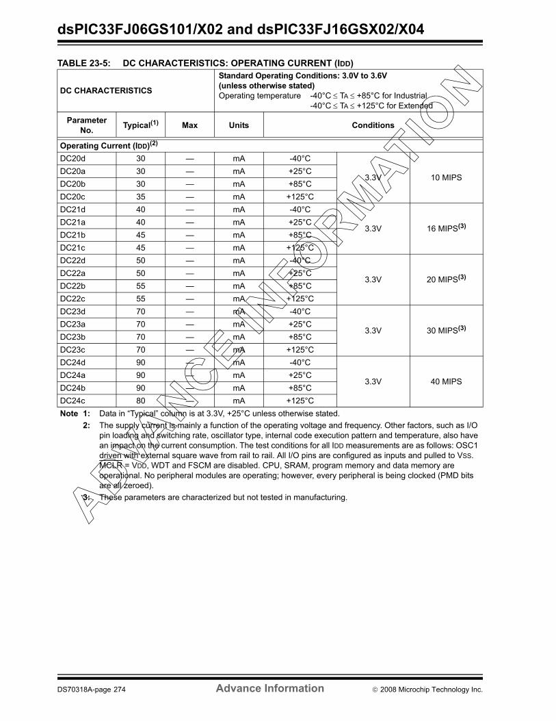
dsPIC33FJ06GS101/X02 and dsPIC33FJ16GSX02/X04
TABLE 23-5: DC CHARACTERISTICS: OPERATING CURRENT (IDD)
DC CHARACTERISTICS
Standard Operating Conditions: 3.0V to 3.6V(unless otherwise stated)Operating temperature -40°C ≤ TA ≤ +85°C for Industrial
-40°C ≤ TA ≤ +125°C for Extended
Parameter No. Typical(1) Max Units Conditions
Operating Current (IDD)(2)
DC20d 30 — mA -40°C
3.3V 10 MIPSDC20a 30 — mA +25°CDC20b 30 — mA +85°CDC20c 35 — mA +125°CDC21d 40 — mA -40°C
3.3V 16 MIPS(3)DC21a 40 — mA +25°CDC21b 45 — mA +85°CDC21c 45 — mA +125°CDC22d 50 — mA -40°C
3.3V 20 MIPS(3)DC22a 50 — mA +25°CDC22b 55 — mA +85°CDC22c 55 — mA +125°CDC23d 70 — mA -40°C
3.3V 30 MIPS(3)DC23a 70 — mA +25°CDC23b 70 — mA +85°CDC23c 70 — mA +125°CDC24d 90 — mA -40°C
3.3V 40 MIPSDC24a 90 — mA +25°CDC24b 90 — mA +85°CDC24c 80 — mA +125°CNote 1: Data in “Typical” column is at 3.3V, +25°C unless otherwise stated.
2: The supply current is mainly a function of the operating voltage and frequency. Other factors, such as I/O pin loading and switching rate, oscillator type, internal code execution pattern and temperature, also have an impact on the current consumption. The test conditions for all IDD measurements are as follows: OSC1 driven with external square wave from rail to rail. All I/O pins are configured as inputs and pulled to VSS. MCLR = VDD, WDT and FSCM are disabled. CPU, SRAM, program memory and data memory are operational. No peripheral modules are operating; however, every peripheral is being clocked (PMD bits are all zeroed).
3: These parameters are characterized but not tested in manufacturing.
DS70318A-page 274 Advance Information © 2008 Microchip Technology Inc.

dsPIC33FJ06GS101/X02 and dsPIC33FJ16GSX02/X04
TABLE 23-6: DC CHARACTERISTICS: IDLE CURRENT (IIDLE)
DC CHARACTERISTICS
Standard Operating Conditions: 3.0V to 3.6V(unless otherwise stated)Operating temperature -40°C ≤ TA ≤ +85°C for Industrial
-40°C ≤ TA ≤ +125°C for Extended
Parameter No. Typical(1) Max Units Conditions
Idle Current (IIDLE): Core OFF Clock ON Base Current(2)
DC40d 3 — mA -40°C
3.3V 10 MIPSDC40a 3 — mA +25°CDC40b 3 — mA +85°CDC40c 3 — mA +125°CDC41d 4 — mA -40°C
3.3V 16 MIPS(3)DC41a 4 mA +25°C—DC41b 5 — mA +85°CDC41c 5 — mA +125°CDC42d 6 — mA -40°C
3.3V 20 MIPS(3)DC42a 6 — mA +25°CDC42b 7 — mA +85°CDC42c 7 — mA +125°CDC43d 9 — mA -40°C
3.3V 30 MIPS(3)DC43a 9 — mA +25°CDC43b 9 — mA +85°CDC43c 9 — mA +125°CDC44d 10 — mA -40°C
3.3V 40 MIPSDC44a 10 — mA +25°CDC44b 16 — mA +85°CDC44c 10 — mA +125°CNote 1: Data in “Typical” column is at 3.3V, +25°C unless otherwise stated.
2: Base IIDLE current is measured with core off, clock on and all modules turned off. Peripheral Module Disable SFR registers are zeroed. All I/O pins are configured as inputs and pulled to VSS.
3: These parameters are characterized but not tested in manufacturing.
© 2008 Microchip Technology Inc. Advance Information DS70318A-page 275

dsPIC33FJ06GS101/X02 and dsPIC33FJ16GSX02/X04
TABLE 23-7: DC CHARACTERISTICS: POWER-DOWN CURRENT (IPD)
DC CHARACTERISTICS
Standard Operating Conditions: 3.0V to 3.6V(unless otherwise stated)Operating temperature -40°C ≤ TA ≤ +85°C for Industrial
-40°C ≤ TA ≤ +125°C for Extended
Parameter No. Typical(1) Max Units Conditions
Power-Down Current (IPD)(2)
DC60d 55 — μA -40°C
3.3V Base Power-Down Current(3,4)DC60a 211 — μA +25°CDC60b 244 — μA +85°CDC60c 245 — μA +125°CDC61d 8 — μA -40°C
3.3V Watchdog Timer Current: ΔIWDT(3)DC61a 10 — μA +25°CDC61b 12 — μA +85°CDC61c 13 — μA +125°CNote 1: Data in the Typical column is at 3.3V, +25°C unless otherwise stated.
2: Base IPD is measured with all peripherals and clocks shut down. All I/Os are configured as inputs and pulled to VSS. WDT, etc., are all switched off.
3: The Δ current is the additional current consumed when the module is enabled. This current should be added to the base IPD current.
4: These currents are measured on the device containing the most memory in this family.
TABLE 23-8: DC CHARACTERISTICS: DOZE CURRENT (IDOZE)
DC CHARACTERISTICS
Standard Operating Conditions: 3.0V to 3.6V(unless otherwise stated)Operating temperature -40°C ≤ TA ≤ +85°C for Industrial
-40°C ≤ TA ≤ +125°C for Extended
Parameter No. Typical(1) Max Doze Ratio Units Conditions
DC73a 25 — 1:2 mA-40°C 3.3V 40 MIPSDC73f 23 — 1:64 mA
DC73g 23 — 1:128 mADC70a 42 — 1:2 mA
+25°C 3.3V 40 MIPSDC70f 26 — 1:64 mADC70g 25 — 1:128 mADC71a 41 — 1:2 mA
+85°C 3.3V 40 MIPSDC71f 25 — 1:64 mADC71g 24 — 1:128 mADC72a 42 — 1:2 mA
+125°C 3.3V 40 MIPSDC72f 26 — 1:64 mADC72g 25 — 1:128 mA
Note 1: Data in the Typical column is at 3.3V, +25°C unless otherwise stated.
DS70318A-page 276 Advance Information © 2008 Microchip Technology Inc.

dsPIC33FJ06GS101/X02 and dsPIC33FJ16GSX02/X04
TABLE 23-9: DC CHARACTERISTICS: I/O PIN INPUT SPECIFICATIONS
DC CHARACTERISTICS
Standard Operating Conditions: 3.0V to 3.6V(unless otherwise stated)Operating temperature -40°C ≤ TA ≤ +85°C for Industrial
-40°C ≤ TA ≤ +125°C for Extended
Param No. Symbol Characteristic Min Typ(1) Max Units Conditions
VIL Input Low VoltageDI10 I/O pins VSS — 0.2 VDD V
DI15 MCLR VSS — 0.2 VDD VDI16 OSC1 (XT mode) VSS — 0.2 VDD VDI17 OSC1 (HS mode) VSS — 0.2 VDD VDI18 SDAx, SCLx VSS — 0.3 VDD V SMbus disabledDI19 SDAx, SCLx VSS — 0.2 VDD V SMbus enabled
VIH Input High VoltageDI20 I/O pins:
with analog functions digital-only
0.8 VDD0.8 VDD
——
VDD5.5
VV
DI25 MCLR 0.8 VDD — VDD VDI26 OSC1 (XT mode) 0.7 VDD — VDD VDI27 OSC1 (HS mode) 0.7 VDD — VDD VDI28 SDAx, SCLx 0.7 VDD — VDD V SMbus disabledDI29 SDAx, SCLx 0.8 VDD — VDD V SMbus enabled
ICNPU CNx Pull-up CurrentDI30 — 250 — μA VDD = 3.3V, VPIN = VSS
IIL Input Leakage Current(2,3)
DI50 I/O Ports:4 mA Source/Sink Capability
8 mA Source/Sink Capability
16 mA Source/Sink Capability
—
—
—
±2
±4
±8
—
—
—
μA
μA
μA
VSS ≤ VPIN ≤ VDD,Pin at high-impedanceVSS ≤ VPIN ≤ VDD,Pin at high-impedanceVSS ≤ VPIN ≤ VDD,Pin at high-impedance
DI51 Analog Input Pins — — ±1 μA VSS ≤ VPIN ≤ VDD, Pin at high-impedance, 40°C ≤ TA ≤ +85°C
DI51b Analog Input Pins — — ±3.5 μA VSS ≤ VPIN ≤ VDD, Pin at high-impedance, -40°C ≤ TA ≤ +125°C
DI55 MCLR — — ±2 μA VSS ≤ VPIN ≤ VDD
DI56 OSC1 — — ±2 μA VSS ≤ VPIN ≤ VDD, XT and HS modes
Note 1: Data in “Typ” column is at 3.3V, +25°C unless otherwise stated.2: The leakage current on the MCLR pin is strongly dependent on the applied voltage level. The specified
levels represent normal operating conditions. Higher leakage current may be measured at different input voltages.
3: Negative current is defined as current sourced by the pin.
© 2008 Microchip Technology Inc. Advance Information DS70318A-page 277

dsPIC33FJ06GS101/X02 and dsPIC33FJ16GSX02/X04
TABLE 23-10: DC CHARACTERISTICS: I/O PIN OUTPUT SPECIFICATIONS
DC CHARACTERISTICS
Standard Operating Conditions: 3.0V to 3.6V(unless otherwise stated)Operating temperature -40°C ≤ TA ≤ +85°C for Industrial
-40°C ≤ TA ≤ +125°C for Extended
Param No. Symbol Characteristic Min Typ Max Units Conditions
DO10 VOL Output Low VoltageI/O ports:
4 mA Source/Sink Capability8 mA Source/Sink Capability16 mA Source/Sink Capability
———
0.40.40.4
———
VVV
IOL = 4 mA, VDD = 3.3VIOL = 8 mA, VDD = 3.3VIOL = 16 mA, VDD = 3.3V
DO16 OSC2/CLKO — 0.4 — V IOL = 2 mA, VDD = 3.3VDO20 VOH Output High Voltage
I/O ports:4 mA Source/Sink Capability8 mA Source/Sink Capability16 mA Source/Sink Capability
———
2.402.402.40
———
VVV
IOH = -4 mA, VDD = 3.3VIOH = -8 mA, VDD = 3.3VIOH = -16 mA, VDD = 3.3V
DO26 OSC2/CLKO — 2.41 — V IOH = -1.3 mA, VDD = 3.3V
TABLE 23-11: ELECTRICAL CHARACTERISTICS: BOR
DC CHARACTERISTICS
Standard Operating Conditions: 3.0V to 3.6V(unless otherwise stated)Operating temperature -40°C ≤ TA ≤ +85°C for Industrial
-40°C ≤ TA ≤ +125°C for Extended
ParamNo. Symbol Characteristic Min(1) Typ Max Units Conditions
BO10 VBOR BOR Event on VDD transition high-to-lowBOR event is tied to VDD core voltage decrease
2.55 — 2.75 V
Note 1: Parameters are for design guidance only and are not tested in manufacturing.
DS70318A-page 278 Advance Information © 2008 Microchip Technology Inc.

dsPIC33FJ06GS101/X02 and dsPIC33FJ16GSX02/X04
TABLE 23-13: INTERNAL VOLTAGE REGULATOR SPECIFICATIONS
TABLE 23-12: DC CHARACTERISTICS: PROGRAM MEMORY
DC CHARACTERISTICS
Standard Operating Conditions: 3.0V to 3.6V(unless otherwise stated)Operating temperature -40°C ≤ TA ≤ +85°C for Industrial
-40°C ≤ TA ≤ +125°C for Extended
ParamNo. Symbol Characteristic Min Typ(1) Max Units Conditions
Program Flash MemoryD130 EP Cell Endurance 10,000 — — E/W -40°C to +125°CD131 VPR VDD for Read VMIN — 3.6 V VMIN = Minimum operating
voltageD132B VPEW VDD for Self-Timed Write VMIN — 3.6 V VMIN = Minimum operating
voltageD134 TRETD Characteristic Retention 20 — — Year Provided no other specifications
are violated, -40°C to +125°CD135 IDDP Supply Current during
Programming— 10 — mA
D136 TRW Row Write Time — 1.6 — msD137 TPE Page Erase Time — 20 — msD138 TWW Word Write Cycle Time 20 — 40 μsNote 1: Data in “Typ” column is at 3.3V, +25°C unless otherwise stated.
Operating Conditions: -40°C < TA < +85°C (unless otherwise stated)
ParamNo. Symbol Characteristics Min Typ Max Units Comments
CEFC External Filter Capacitor Value
1 10 — μF Capacitor must be low series resistance (< 5 ohms)
© 2008 Microchip Technology Inc. Advance Information DS70318A-page 279

dsPIC33FJ06GS101/X02 and dsPIC33FJ16GSX02/X04
23.2 AC Characteristics and Timing Parameters This section defines dsPIC33FJ06GS101/X02 and dsPIC33FJ16GSX02/X04 AC characteristics and timing parameters.
TABLE 23-14: TEMPERATURE AND VOLTAGE SPECIFICATIONS – AC
FIGURE 23-1: LOAD CONDITIONS FOR DEVICE TIMING SPECIFICATIONS
TABLE 23-15: CAPACITIVE LOADING REQUIREMENTS ON OUTPUT PINS
AC CHARACTERISTICS
Standard Operating Conditions: 3.0V to 3.6V(unless otherwise stated)Operating temperature -40°C ≤ TA ≤ +85°C for Industrial
-40°C ≤ TA ≤ +125°C for ExtendedOperating voltage VDD range as described in Section 23.0 “Electrical Characteristics”.
Param No. Symbol Characteristic Min Typ Max Units Conditions
DO50 COSC2 OSC2 pin — — 15 pF In XT and HS modes when external clock is used to drive OSC1
DO56 CIO All I/O pins and OSC2 — — 50 pF EC mode DO58 CB SCLx, SDAx — — 400 pF In I2C™ mode
VDD/2
CL
RL
Pin
Pin
VSS
VSS
CL
RL = 464ΩCL = 50 pF for all pins except OSC2
15 pF for OSC2 output
Load Condition 1 – for all pins except OSC2 Load Condition 2 – for OSC2
DS70318A-page 280 Advance Information © 2008 Microchip Technology Inc.

dsPIC33FJ06GS101/X02 and dsPIC33FJ16GSX02/X04
FIGURE 23-2: EXTERNAL CLOCK TIMING
Q1 Q2 Q3 Q4
OSC1
CLKO
Q1 Q2 Q3 Q4
OS20
OS25OS30 OS30
OS40OS41
OS31 OS31
TABLE 23-16: EXTERNAL CLOCK TIMING REQUIREMENTS
AC CHARACTERISTICS
Standard Operating Conditions: 3.0V to 3.6V(unless otherwise stated)Operating temperature -40°C ≤ TA ≤ +85°C for Industrial
-40°C ≤ TA ≤ +125°C for Extended
ParamNo. Symb Characteristic Min Typ(1) Max Units Conditions
OS10 FIN External CLKI Frequency(External clocks allowed onlyin EC and ECPLL modes)
DC — 40 MHz EC
Oscillator Crystal Frequency 3.510
——
1040
MHzMHz
XTHS
OS20 TOSC TOSC = 1/FOSC 12.5 — DC nsOS25 TCY Instruction Cycle Time(2) 25 — DC nsOS30 TosL,
TosHExternal Clock in (OSC1)High or Low Time
0.375 x TOSC — 0.625 x TOSC ns EC
OS31 TosR,TosF
External Clock in (OSC1)Rise or Fall Time
— — 20 ns EC
OS40 TckR CLKO Rise Time(3) — 5.2 — nsOS41 TckF CLKO Fall Time(3) — 5.2 — nsNote 1: Data in “Typ” column is at 3.3V, +25°C unless otherwise stated.
2: Instruction cycle period (TCY) equals two times the input oscillator time-base period. All specified values are based on characterization data for that particular oscillator type under standard operating conditions with the device executing code. Exceeding these specified limits may result in an unstable oscillator operation and/or higher than expected current consumption. All devices are tested to operate at “min.” values with an external clock applied to the OSC1/CLKI pin. When an external clock input is used, the “max.” cycle time limit is “DC” (no clock) for all devices.
3: Measurements are taken in EC mode. The CLKO signal is measured on the OSC2 pin.
© 2008 Microchip Technology Inc. Advance Information DS70318A-page 281

dsPIC33FJ06GS101/X02 and dsPIC33FJ16GSX02/X04
TABLE 23-17: PLL CLOCK TIMING SPECIFICATIONS (VDD = 3.0V TO 3.6V)
AC CHARACTERISTICSStandard Operating Conditions: 3.0V to 3.6V (unless otherwise stated)Operating temperature -40°C ≤ TA ≤ +85°C for Industrial
-40°C ≤ TA ≤ +125°C for Extended
ParamNo. Symbol Characteristic Min Typ(1) Max Units Conditions
OS50 FPLLI PLL Voltage Controlled Oscillator (VCO) Input Frequency Range
0.8 — 8 MHz ECPLL, XTPLL modes
OS51 FSYS On-Chip VCO System Frequency
100 — 200 MHz
OS52 TLOCK PLL Start-up Time (Lock Time) 0.9 1.5 3.1 mSOS53 DCLK CLKO Stability (Jitter) -3 0.5 3 % Measured over 100 ms
periodNote 1: Data in “Typ” column is at 3.3V, +25°C unless otherwise stated. Parameters are for design guidance only
and are not tested in manufacturing.
TABLE 23-18: AUXILIARY PLL CLOCK TIMING SPECIFICATIONS (VDD = 3.0V TO 3.6V)
AC CHARACTERISTICSStandard Operating Conditions: 3.0V to 3.6V (unless otherwise stated)Operating temperature -40°C ≤ TA ≤ +85°C for Industrial
-40°C ≤ TA ≤ +125°C for Extended
ParamNo. Symbol Characteristic Min Typ(1) Max Units Conditions
FHPOUT 0n-chip 16x-PLL CCO fre-quency
105 120 135 MHz
FHPIN On-chip 16x-PLL Phase Detec-tor input frequency
6.56 7.5 8.44 MHz
TSU Frequency generator lock time — — 10 µsNote 1: Data in “Typ” column is at 3.3V, +25°C unless otherwise stated. Parameters are for design guidance only
and are not tested in manufacturing.
TABLE 23-19: AC CHARACTERISTICS: INTERNAL RC ACCURACY
AC CHARACTERISTICS Standard Operating Conditions: 3.0V to 3.6V (unless otherwise stated)Operating temperature -40°C ≤ TA ≤ +85°C for industrial
Param No. Characteristic Min Typ Max Units Conditions
Internal FRC Accuracy @ FRC Frequency = 7.37 MHz(1,2)
F20 FRC — ±1 — % -40°C ≤ TA ≤ +85°C VDD = 3.0-3.6VFRC — ±2 — % -40°C ≤ TA ≤ +125°C VDD = 3.0-3.6V
Note 1: Frequency calibrated at +25°C and 3.3V. TUN bits can be used to compensate for temperature drift.2: FRC is set to initial frequency of 7.37 MHz (±2%) at +25°C.
DS70318A-page 282 Advance Information © 2008 Microchip Technology Inc.

dsPIC33FJ06GS101/X02 and dsPIC33FJ16GSX02/X04
FIGURE 23-3: I/O TIMING CHARACTERISTICS
TABLE 23-20: INTERNAL RC ACCURACY
AC CHARACTERISTICSStandard Operating Conditions: 3.0V to 3.6V (unless otherwise stated)Operating temperature -40°C ≤ TA ≤ +85°C for Industrial
-40°C ≤ TA ≤ +125°C for Extended
ParamNo. Characteristic Min Typ Max Units Conditions
LPRC @ 32.768 kHz(1)
F21 LPRC -20 ±6 +20 % -40°C ≤ TA ≤ +85°C VDD = 3.0-3.6VLPRC -70 — +70 % -40°C ≤ TA ≤ +125°C VDD = 3.0-3.6V
Note 1: Change of LPRC frequency as VDD changes.
Note: Refer to Figure 23-1 for load conditions.
I/O Pin(Input)
I/O Pin(Output)
DI35
Old Value New Value
DI40
DO31DO32
TABLE 23-21: I/O TIMING REQUIREMENTS
AC CHARACTERISTICS
Standard Operating Conditions: 3.0V to 3.6V(unless otherwise stated)Operating temperature -40°C ≤ TA ≤ +85°C for Industrial
-40°C ≤ TA ≤ +125°C for Extended
ParamNo. Symbol Characteristic Min Typ(1) Max Units Conditions
DO31 TIOR Port Output Rise Time — 10 25 ns Refer to Figure 23-1 for test conditions
DO32 TIOF Port Output Fall Time — 10 25 ns Refer to Figure 23-1 for test conditions
DI35 TINP INTx Pin High or Low Time (output) 20 — — nsDI40 TRBP CNx High or Low Time (input) 2 — — TCY
Note 1: Data in “Typ” column is at 3.3V, +25°C unless otherwise stated.
© 2008 Microchip Technology Inc. Advance Information DS70318A-page 283
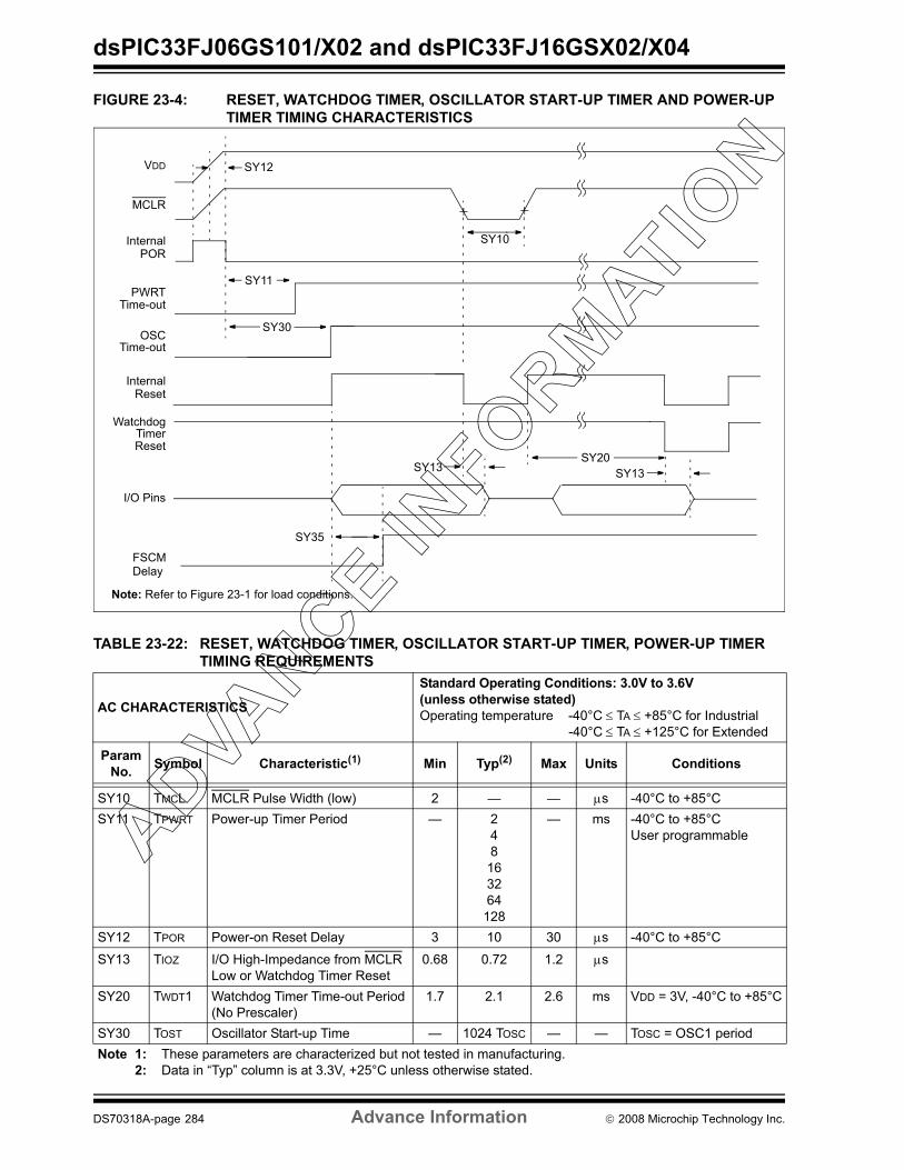
dsPIC33FJ06GS101/X02 and dsPIC33FJ16GSX02/X04
FIGURE 23-4: RESET, WATCHDOG TIMER, OSCILLATOR START-UP TIMER AND POWER-UP TIMER TIMING CHARACTERISTICS
TABLE 23-22: RESET, WATCHDOG TIMER, OSCILLATOR START-UP TIMER, POWER-UP TIMER TIMING REQUIREMENTS
AC CHARACTERISTICS
Standard Operating Conditions: 3.0V to 3.6V(unless otherwise stated)Operating temperature -40°C ≤ TA ≤ +85°C for Industrial
-40°C ≤ TA ≤ +125°C for Extended
ParamNo. Symbol Characteristic(1) Min Typ(2) Max Units Conditions
SY10 TMCL MCLR Pulse Width (low) 2 — — μs -40°C to +85°CSY11 TPWRT Power-up Timer Period — 2
48163264
128
— ms -40°C to +85°CUser programmable
SY12 TPOR Power-on Reset Delay 3 10 30 μs -40°C to +85°C
SY13 TIOZ I/O High-Impedance from MCLR Low or Watchdog Timer Reset
0.68 0.72 1.2 μs
SY20 TWDT1 Watchdog Timer Time-out Period (No Prescaler)
1.7 2.1 2.6 ms VDD = 3V, -40°C to +85°C
SY30 TOST Oscillator Start-up Time — 1024 TOSC — — TOSC = OSC1 periodNote 1: These parameters are characterized but not tested in manufacturing.
2: Data in “Typ” column is at 3.3V, +25°C unless otherwise stated.
VDD
MCLR
InternalPOR
PWRTTime-out
OSCTime-out
InternalReset
WatchdogTimerReset
SY11
SY10
SY20SY13
I/O Pins
SY13
Note: Refer to Figure 23-1 for load conditions.
FSCM Delay
SY35
SY30
SY12
DS70318A-page 284 Advance Information © 2008 Microchip Technology Inc.

dsPIC33FJ06GS101/X02 and dsPIC33FJ16GSX02/X04
FIGURE 23-5: TIMER1, 2 AND 3 EXTERNAL CLOCK TIMING CHARACTERISTICS
Note: Refer to Figure 23-1 for load conditions.
Tx11
Tx15
Tx10
Tx20
TMRxOS60
TxCK
TABLE 23-23: TIMER1 EXTERNAL CLOCK TIMING REQUIREMENTS(1)
AC CHARACTERISTICS
Standard Operating Conditions: 3.0V to 3.6V(unless otherwise stated)Operating temperature -40°C ≤ TA ≤ +85°C for Industrial
-40°C ≤ TA ≤ +125°C for Extended
ParamNo. Symbol Characteristic Min Typ Max Units Conditions
TA10 TTXH TxCK High Time Synchronous,no prescaler
0.5 TCY + 20 — — ns Must also meet parameter TA15
Synchronous,with prescaler
10 — — ns
Asynchronous 10 — — nsTA11 TTXL TxCK Low Time Synchronous,
no prescaler0.5 TCY + 20 — — ns Must also meet
parameter TA15Synchronous,with prescaler
10 — — ns
Asynchronous 10 — — nsTA15 TTXP TxCK Input Period Synchronous,
no prescalerTCY + 40 — — ns
Synchronous,with prescaler
Greater of:20 ns or
(TCY + 40)/N
— — — N = prescale value(1, 8, 64, 256)
Asynchronous 20 — — nsOS60 Ft1 T1CK Oscillator Input frequency
Range (oscillator enabled by setting bit TCS (T1CON<1>))
DC — 50 kHz
TA20 TCKEXTMRL Delay from External TxCK Clock Edge to Timer Increment
0.5 TCY 1.5 TCY —
Note 1: Timer1 is a Type A.
© 2008 Microchip Technology Inc. Advance Information DS70318A-page 285
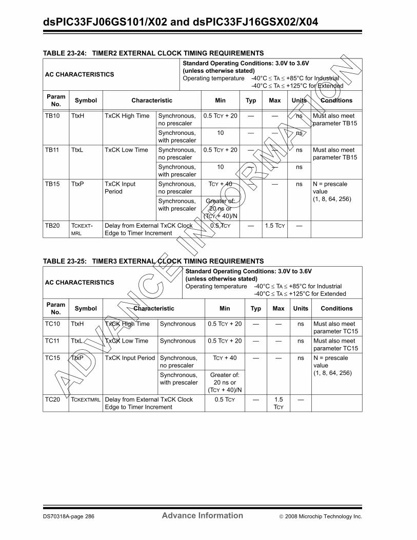
dsPIC33FJ06GS101/X02 and dsPIC33FJ16GSX02/X04
TABLE 23-24: TIMER2 EXTERNAL CLOCK TIMING REQUIREMENTS
AC CHARACTERISTICS
Standard Operating Conditions: 3.0V to 3.6V(unless otherwise stated)Operating temperature -40°C ≤ TA ≤ +85°C for Industrial
-40°C ≤ TA ≤ +125°C for Extended
ParamNo. Symbol Characteristic Min Typ Max Units Conditions
TB10 TtxH TxCK High Time Synchronous,no prescaler
0.5 TCY + 20 — — ns Must also meet parameter TB15
Synchronous,with prescaler
10 — — ns
TB11 TtxL TxCK Low Time Synchronous,no prescaler
0.5 TCY + 20 — — ns Must also meet parameter TB15
Synchronous,with prescaler
10 — — ns
TB15 TtxP TxCK Input Period
Synchronous,no prescaler
TCY + 40 — — ns N = prescale value(1, 8, 64, 256)Synchronous,
with prescalerGreater of:
20 ns or(TCY + 40)/N
TB20 TCKEXT-MRL
Delay from External TxCK Clock Edge to Timer Increment
0.5 TCY — 1.5 TCY —
TABLE 23-25: TIMER3 EXTERNAL CLOCK TIMING REQUIREMENTS
AC CHARACTERISTICS
Standard Operating Conditions: 3.0V to 3.6V(unless otherwise stated)Operating temperature -40°C ≤ TA ≤ +85°C for Industrial
-40°C ≤ TA ≤ +125°C for Extended
ParamNo. Symbol Characteristic Min Typ Max Units Conditions
TC10 TtxH TxCK High Time Synchronous 0.5 TCY + 20 — — ns Must also meet parameter TC15
TC11 TtxL TxCK Low Time Synchronous 0.5 TCY + 20 — — ns Must also meet parameter TC15
TC15 TtxP TxCK Input Period Synchronous,no prescaler
TCY + 40 — — ns N = prescalevalue (1, 8, 64, 256)Synchronous,
with prescalerGreater of:
20 ns or (TCY + 40)/N
TC20 TCKEXTMRL Delay from External TxCK Clock Edge to Timer Increment
0.5 TCY — 1.5 TCY
—
DS70318A-page 286 Advance Information © 2008 Microchip Technology Inc.

dsPIC33FJ06GS101/X02 and dsPIC33FJ16GSX02/X04
FIGURE 23-6: INPUT CAPTURE (CAPx) TIMING CHARACTERISTICS
FIGURE 23-7: OUTPUT COMPARE MODULE (OCx) TIMING CHARACTERISTICS
TABLE 23-26: INPUT CAPTURE TIMING REQUIREMENTS
AC CHARACTERISTICS
Standard Operating Conditions: 3.0V to 3.6V(unless otherwise stated)Operating temperature -40°C ≤ TA ≤ +85°C for Industrial
-40°C ≤ TA ≤ +125°C for Extended
ParamNo. Symbol Characteristic(1) Min Max Units Conditions
IC10 TccL ICx Input Low Time No Prescaler 0.5 TCY + 20 — nsWith Prescaler 10 — ns
IC11 TccH ICx Input High Time No Prescaler 0.5 TCY + 20 — nsWith Prescaler 10 — ns
IC15 TccP ICx Input Period (TCY + 40)/N — ns N = prescale value (1, 4, 16)
Note 1: These parameters are characterized but not tested in manufacturing.
TABLE 23-27: OUTPUT COMPARE MODULE TIMING REQUIREMENTS
AC CHARACTERISTICS
Standard Operating Conditions: 3.0V to 3.6V(unless otherwise stated)Operating temperature -40°C ≤ TA ≤ +85°C for Industrial
-40°C ≤ TA ≤ +125°C for Extended
Param No. Symbol Characteristic(1) Min Typ Max Units Conditions
OC10 TccF OCx Output Fall Time — — — ns See parameter D032OC11 TccR OCx Output Rise Time — — — ns See parameter D031Note 1: These parameters are characterized but not tested in manufacturing.
ICx
IC10 IC11
IC15
Note: Refer to Figure 23-1 for load conditions.
OCx
OC11 OC10(Output Compare
Note: Refer to Figure 23-1 for load conditions.
or PWM Mode)
© 2008 Microchip Technology Inc. Advance Information DS70318A-page 287

dsPIC33FJ06GS101/X02 and dsPIC33FJ16GSX02/X04
FIGURE 23-8: OC/PWM MODULE TIMING CHARACTERISTICS
OCFA
OCx
OC20
OC15
TABLE 23-28: SIMPLE OC/PWM MODE TIMING REQUIREMENTS
AC CHARACTERISTICS
Standard Operating Conditions: 3.0V to 3.6V(unless otherwise stated)Operating temperature -40°C ≤ TA ≤ +85°C for Industrial
-40°C ≤ TA ≤ +125°C for Extended
Param No. Symbol Characteristic(1) Min Typ Max Units Conditions
OC15 TFD Fault Input to PWM I/O Change
— — 50 ns —
OC20 TFLT Fault Input Pulse Width 50 — — ns —Note 1: These parameters are characterized but not tested in manufacturing.
DS70318A-page 288 Advance Information © 2008 Microchip Technology Inc.

dsPIC33FJ06GS101/X02 and dsPIC33FJ16GSX02/X04
FIGURE 23-9: HIGH-SPEED PWM MODULE FAULT TIMING CHARACTERISTICS
FIGURE 23-10: HIGH-SPEED PWM MODULE TIMING CHARACTERISTICS
FLTx
PWMx
MP30
MP20
PWMx
MP11 MP10
Note: Refer to Figure 23-1 for load conditions.
TABLE 23-29: HIGH-SPEED PWM MODULE TIMING REQUIREMENTS
AC CHARACTERISTICS
Standard Operating Conditions: 3.0V to 3.6V(unless otherwise stated)Operating temperature -40°C ≤ TA ≤ +85°C for Industrial
-40°C ≤ TA ≤ +125°C for Extended
ParamNo. Symbol Characteristic(1) Min Typ Max Units Conditions
MP10 TFPWM PWM Output Fall Time — 2.5 — ns See parameter D032MP11 TRPWM PWM Output Rise Time — 2.5 — ns See parameter D031
MP20 TFD Fault Input ↓ to PWMI/O Change
— — 15 ns —
MP30 TFH Minimum Pulse Width — 8 — ns —
Note 1: These parameters are characterized but not tested in manufacturing.
© 2008 Microchip Technology Inc. Advance Information DS70318A-page 289
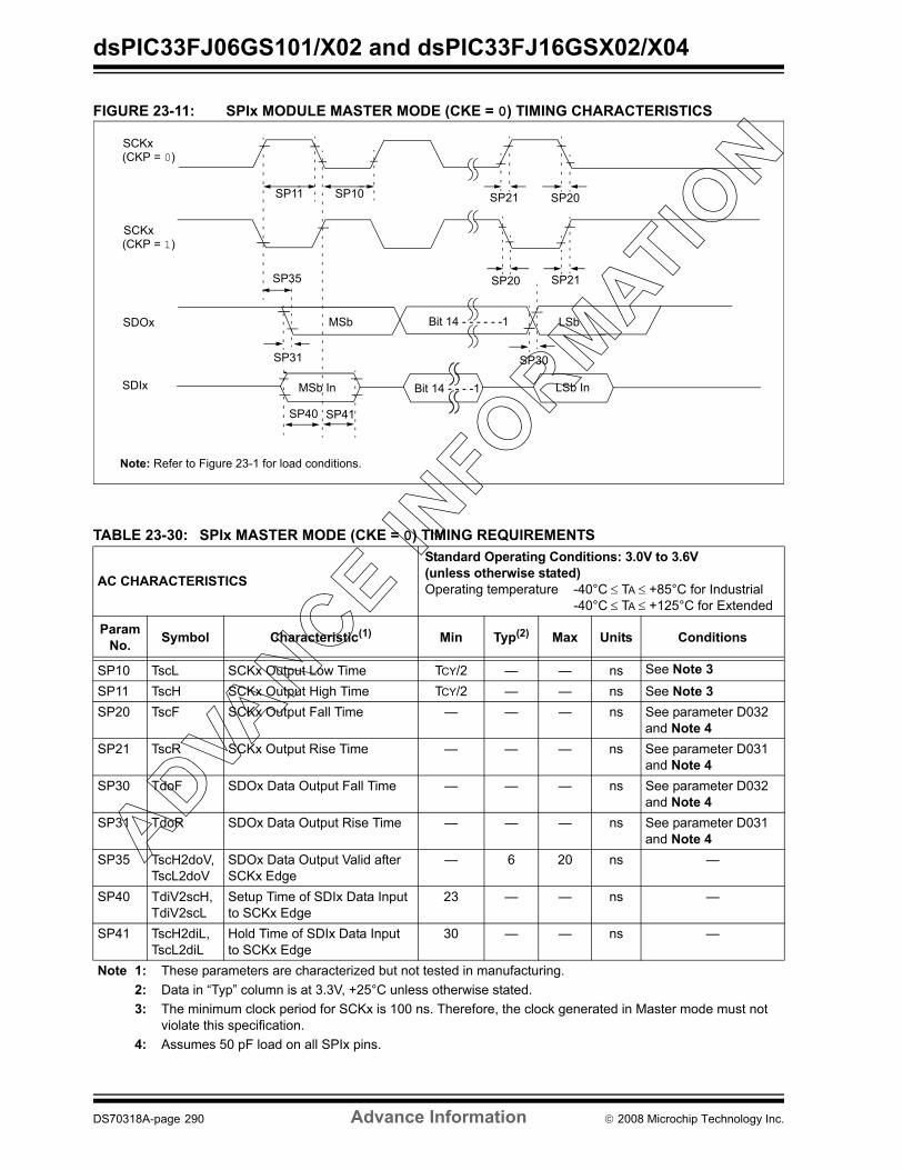
dsPIC33FJ06GS101/X02 and dsPIC33FJ16GSX02/X04
FIGURE 23-11: SPIx MODULE MASTER MODE (CKE = 0) TIMING CHARACTERISTICS
SCKx(CKP = 0)
SCKx(CKP = 1)
SDOx
SDIx
SP11 SP10
SP40 SP41
SP21SP20SP35
SP20SP21
MSb LSbBit 14 - - - - - -1
MSb In LSb InBit 14 - - - -1
SP30SP31
Note: Refer to Figure 23-1 for load conditions.
TABLE 23-30: SPIx MASTER MODE (CKE = 0) TIMING REQUIREMENTS
AC CHARACTERISTICS
Standard Operating Conditions: 3.0V to 3.6V(unless otherwise stated)Operating temperature -40°C ≤ TA ≤ +85°C for Industrial
-40°C ≤ TA ≤ +125°C for Extended
ParamNo. Symbol Characteristic(1) Min Typ(2) Max Units Conditions
SP10 TscL SCKx Output Low Time TCY/2 — — ns See Note 3SP11 TscH SCKx Output High Time TCY/2 — — ns See Note 3SP20 TscF SCKx Output Fall Time — — — ns See parameter D032
and Note 4SP21 TscR SCKx Output Rise Time — — — ns See parameter D031
and Note 4SP30 TdoF SDOx Data Output Fall Time — — — ns See parameter D032
and Note 4SP31 TdoR SDOx Data Output Rise Time — — — ns See parameter D031
and Note 4SP35 TscH2doV,
TscL2doVSDOx Data Output Valid after SCKx Edge
— 6 20 ns —
SP40 TdiV2scH,TdiV2scL
Setup Time of SDIx Data Inputto SCKx Edge
23 — — ns —
SP41 TscH2diL,TscL2diL
Hold Time of SDIx Data Inputto SCKx Edge
30 — — ns —
Note 1: These parameters are characterized but not tested in manufacturing.2: Data in “Typ” column is at 3.3V, +25°C unless otherwise stated.3: The minimum clock period for SCKx is 100 ns. Therefore, the clock generated in Master mode must not
violate this specification.4: Assumes 50 pF load on all SPIx pins.
DS70318A-page 290 Advance Information © 2008 Microchip Technology Inc.

dsPIC33FJ06GS101/X02 and dsPIC33FJ16GSX02/X04
FIGURE 23-12: SPIx MODULE MASTER MODE (CKE = 1) TIMING CHARACTERISTICS
TABLE 23-31: SPIx MODULE MASTER MODE (CKE = 1) TIMING REQUIREMENTS
AC CHARACTERISTICS
Standard Operating Conditions: 3.0V to 3.6V(unless otherwise stated)Operating temperature -40°C ≤ TA ≤ +85°C for Industrial
-40°C ≤ TA ≤ +125°C for Extended
ParamNo. Symbol Characteristic(1) Min Typ(2) Max Units Conditions
SP10 TscL SCKx Output Low Time TCY/2 — — ns See Note 3SP11 TscH SCKx Output High Time TCY/2 — — ns See Note 3SP20 TscF SCKx Output Fall Time — — — ns See parameter D032
and Note 4SP21 TscR SCKx Output Rise Time — — — ns See parameter D031
and Note 4SP30 TdoF SDOx Data Output Fall Time — — — ns See parameter D032
and Note 4SP31 TdoR SDOx Data Output Rise Time — — — ns See parameter D031
and Note 4SP35 TscH2doV,
TscL2doVSDOx Data Output Valid afterSCKx Edge
— 6 20 ns —
SP36 TdoV2sc, TdoV2scL
SDOx Data Output Setup toFirst SCKx Edge
30 — — ns —
SP40 TdiV2scH, TdiV2scL
Setup Time of SDIx Data Input to SCKx Edge
23 — — ns —
SP41 TscH2diL, TscL2diL
Hold Time of SDIx Data Inputto SCKx Edge
30 — — ns —
Note 1: These parameters are characterized but not tested in manufacturing.2: Data in “Typ” column is at 3.3V, +25°C unless otherwise stated.3: The minimum clock period for SCKx is 100 ns. The clock generated in Master mode must not violate this
specification.4: Assumes 50 pF load on all SPIx pins.
SCKX(CKP = 0)
SCKX(CKP = 1)
SDOX
SDIX
SP36
SP30,SP31
SP35
MSb
MSb In
Bit 14 - - - - - -1
LSb InBit 14 - - - -1
LSb
Note: Refer to Figure 23-1 for load conditions.
SP11 SP10 SP20SP21
SP21SP20
SP40
SP41
© 2008 Microchip Technology Inc. Advance Information DS70318A-page 291

dsPIC33FJ06GS101/X02 and dsPIC33FJ16GSX02/X04
FIGURE 23-13: SPIx MODULE SLAVE MODE (CKE = 0) TIMING CHARACTERISTICS
SSX
SCKX(CKP = 0)
SCKX(CKP = 1)
SDOX
SP50
SP40SP41
SP30,SP31 SP51
SP35
MSb LSbBit 14 - - - - - -1
MSb In Bit 14 - - - -1 LSb In
SP52
SP73SP72
SP72SP73SP71 SP70
Note: Refer to Figure 23-1 for load conditions.
SDIX
TABLE 23-32: SPIx MODULE SLAVE MODE (CKE = 0) TIMING REQUIREMENTS
AC CHARACTERISTICS
Standard Operating Conditions: 3.0V to 3.6V(unless otherwise stated)Operating temperature -40°C ≤ TA ≤ +85°C for Industrial
-40°C ≤ TA ≤ +125°C for Extended
ParamNo. Symbol Characteristic(1) Min Typ(2) Max Units Conditions
SP70 TscL SCKx Input Low Time 30 — — ns —SP71 TscH SCKx Input High Time 30 — — ns —SP72 TscF SCKx Input Fall Time — 10 25 ns See Note 3SP73 TscR SCKx Input Rise Time — 10 25 ns See Note 3SP30 TdoF SDOx Data Output Fall Time — — — ns See parameter D032
and Note 3SP31 TdoR SDOx Data Output Rise Time — — — ns See parameter D031
and Note 3SP35 TscH2doV,
TscL2doVSDOx Data Output Valid after SCKx Edge
— — 30 ns —
SP40 TdiV2scH, TdiV2scL
Setup Time of SDIx Data Input to SCKx Edge
20 — — ns —
SP41 TscH2diL, TscL2diL
Hold Time of SDIx Data Input to SCKx Edge
20 — — ns —
SP50 TssL2scH, TssL2scL
SSx ↓ to SCKx ↑ or SCKx Input 120 — — ns —
SP51 TssH2doZ SSx ↑ to SDOx OutputHigh-Impedance
10 — 50 ns See Note 3
SP52 TscH2ssHTscL2ssH
SSx after SCKx Edge 1.5 TCY +40 — — ns —
Note 1: These parameters are characterized but not tested in manufacturing.2: Data in “Typ” column is at 3.3V, +25°C unless otherwise stated.3: Assumes 50 pF load on all SPIx pins.
DS70318A-page 292 Advance Information © 2008 Microchip Technology Inc.

dsPIC33FJ06GS101/X02 and dsPIC33FJ16GSX02/X04
FIGURE 23-14: SPIx MODULE SLAVE MODE (CKE = 1) TIMING CHARACTERISTICS
SSx
SCKx(CKP = 0)
SCKx(CKP = 1)
SDOx
SDI
SP50
SP60
SDIx
SP30,SP31
MSb Bit 14 - - - - - -1 LSb
SP51
MSb In Bit 14 - - - -1 LSb In
SP35
SP52
SP52
SP73SP72
SP72SP73SP71 SP70
SP40SP41
Note: Refer to Figure 23-1 for load conditions.
© 2008 Microchip Technology Inc. Advance Information DS70318A-page 293

dsPIC33FJ06GS101/X02 and dsPIC33FJ16GSX02/X04
TABLE 23-33: SPIx MODULE SLAVE MODE (CKE = 1) TIMING REQUIREMENTS
AC CHARACTERISTICS
Standard Operating Conditions: 3.0V to 3.6V(unless otherwise stated)Operating temperature -40°C ≤ TA ≤ +85°C for Industrial
-40°C ≤ TA ≤ +125°C for Extended
ParamNo. Symbol Characteristic(1) Min Typ(2) Max Units Conditions
SP70 TscL SCKx Input Low Time 30 — — ns —SP71 TscH SCKx Input High Time 30 — — ns —SP72 TscF SCKx Input Fall Time — 10 25 ns See Note 3SP73 TscR SCKx Input Rise Time — 10 25 ns See Note 3SP30 TdoF SDOx Data Output Fall Time — — — ns See parameter
D032 and Note 3SP31 TdoR SDOx Data Output Rise Time — — — ns See parameter
D031 and Note 3SP35 TscH2doV,
TscL2doVSDOx Data Output Valid afterSCKx Edge
— — 30 ns —
SP40 TdiV2scH, TdiV2scL
Setup Time of SDIx Data Inputto SCKx Edge
20 — — ns —
SP41 TscH2diL, TscL2diL
Hold Time of SDIx Data Inputto SCKx Edge
20 — — ns —
SP50 TssL2scH, TssL2scL
SSx ↓ to SCKx ↓ or SCKx ↑ Input
120 — — ns —
SP51 TssH2doZ SSx ↑ to SDOX OutputHigh-Impedance
10 — 50 ns See Note 4
SP52 TscH2ssHTscL2ssH
SSx ↑ after SCKx Edge 1.5 TCY + 40 — — ns —
SP60 TssL2doV SDOx Data Output Valid afterSSx Edge
— — 50 ns —
Note 1: These parameters are characterized but not tested in manufacturing.2: Data in “Typ” column is at 3.3V, +25°C unless otherwise stated.3: The minimum clock period for SCKx is 100 ns. The clock generated in Master mode must not violate this
specification.4: Assumes 50 pF load on all SPIx pins.
DS70318A-page 294 Advance Information © 2008 Microchip Technology Inc.

dsPIC33FJ06GS101/X02 and dsPIC33FJ16GSX02/X04
FIGURE 23-15: I2Cx BUS START/STOP BITS TIMING CHARACTERISTICS (MASTER MODE)
FIGURE 23-16: I2Cx BUS DATA TIMING CHARACTERISTICS (MASTER MODE)
IM31 IM34SCLx
SDAx
StartCondition
StopCondition
IM30 IM33
Note: Refer to Figure 23-1 for load conditions.
IM11IM10 IM33
IM11IM10
IM20
IM26IM25
IM40 IM40 IM45
IM21
SCLx
SDAxIn
SDAxOut
Note: Refer to Figure 23-1 for load conditions.
© 2008 Microchip Technology Inc. Advance Information DS70318A-page 295

dsPIC33FJ06GS101/X02 and dsPIC33FJ16GSX02/X04
TABLE 23-34: I2Cx BUS DATA TIMING REQUIREMENTS (MASTER MODE)
AC CHARACTERISTICS
Standard Operating Conditions: 3.0V to 3.6V(unless otherwise stated)Operating temperature -40°C ≤ TA ≤ +85°C for Industrial
-40°C ≤ TA ≤ +125°C for Extended
ParamNo. Symbol Characteristic Min(1) Max Units Conditions
IM10 TLO:SCL Clock Low Time 100 kHz mode TCY/2 (BRG + 1) — μs —400 kHz mode TCY/2 (BRG + 1) — μs —1 MHz mode(2) TCY/2 (BRG + 1) — μs —
IM11 THI:SCL Clock High Time 100 kHz mode TCY/2 (BRG + 1) — μs —400 kHz mode TCY/2 (BRG + 1) — μs —1 MHz mode(2) TCY/2 (BRG + 1) — μs —
IM20 TF:SCL SDAx and SCLxFall Time
100 kHz mode — 300 ns CB is specified to be from 10 to 400 pF400 kHz mode 20 + 0.1 CB 300 ns
1 MHz mode(2) — 100 nsIM21 TR:SCL SDAx and SCLx
Rise Time100 kHz mode — 1000 ns CB is specified to be
from 10 to 400 pF400 kHz mode 20 + 0.1 CB 300 ns1 MHz mode(2) — 300 ns
IM25 TSU:DAT Data InputSetup Time
100 kHz mode 250 — ns —400 kHz mode 100 — ns1 MHz mode(2) 40 — ns
IM26 THD:DAT Data InputHold Time
100 kHz mode 0 — μs —400 kHz mode 0 0.9 μs1 MHz mode(2) 0.2 — μs
IM30 TSU:STA Start ConditionSetup Time
100 kHz mode TCY/2 (BRG + 1) — μs Only relevant for Repeated Startcondition
400 kHz mode TCY/2 (BRG + 1) — μs1 MHz mode(2) TCY/2 (BRG + 1) — μs
IM31 THD:STA Start Condition Hold Time
100 kHz mode TCY/2 (BRG + 1) — μs After this period thefirst clock pulse isgenerated
400 kHz mode TCY/2 (BRG + 1) — μs1 MHz mode(2) TCY/2 (BRG + 1) — μs
IM33 TSU:STO Stop Condition Setup Time
100 kHz mode TCY/2 (BRG + 1) — μs —400 kHz mode TCY/2 (BRG + 1) — μs1 MHz mode(2) TCY/2 (BRG + 1) — μs
IM34 THD:STO Stop Condition 100 kHz mode TCY/2 (BRG + 1) — ns —Hold Time 400 kHz mode TCY/2 (BRG + 1) — ns
1 MHz mode(2) TCY/2 (BRG + 1) — nsIM40 TAA:SCL Output Valid
From Clock100 kHz mode — 3500 ns —400 kHz mode — 1000 ns —1 MHz mode(2) — 400 ns —
IM45 TBF:SDA Bus Free Time 100 kHz mode 4.7 — μs Time the bus must be free before a newtransmission can start
400 kHz mode 1.3 — μs1 MHz mode(2) 0.5 — μs
IM50 CB Bus Capacitive Loading — 400 pF Note 1: BRG is the value of the I2C Baud Rate Generator. Refer to Section 19. “Inter-Integrated Circuit (I2C™)”
(DS70195) in the “dsPIC33F Family Reference Manual” available from the Microchip website.2: Maximum pin capacitance = 10 pF for all I2Cx pins (for 1 MHz mode only).
DS70318A-page 296 Advance Information © 2008 Microchip Technology Inc.
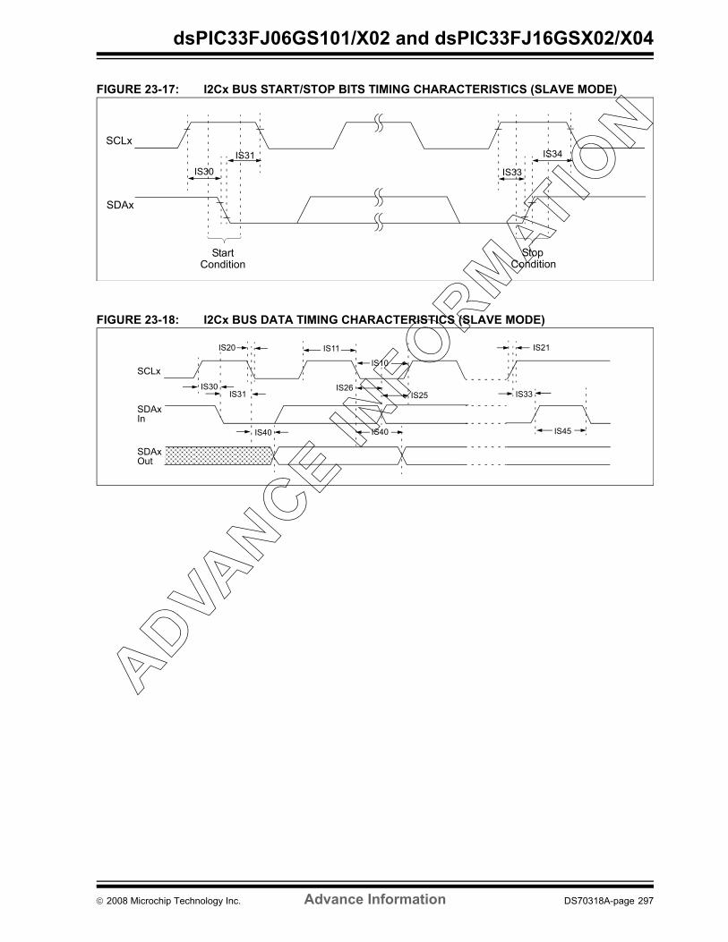
dsPIC33FJ06GS101/X02 and dsPIC33FJ16GSX02/X04
FIGURE 23-17: I2Cx BUS START/STOP BITS TIMING CHARACTERISTICS (SLAVE MODE)
FIGURE 23-18: I2Cx BUS DATA TIMING CHARACTERISTICS (SLAVE MODE)
IS31 IS34SCLx
SDAx
StartCondition
StopCondition
IS30 IS33
IS30IS31 IS33
IS11
IS10
IS20
IS26IS25
IS40 IS40 IS45
IS21
SCLx
SDAxIn
SDAxOut
© 2008 Microchip Technology Inc. Advance Information DS70318A-page 297

dsPIC33FJ06GS101/X02 and dsPIC33FJ16GSX02/X04
TABLE 23-35: I2Cx BUS DATA TIMING REQUIREMENTS (SLAVE MODE)
AC CHARACTERISTICS
Standard Operating Conditions: 3.0V to 3.6V(unless otherwise stated)Operating temperature -40°C ≤ TA ≤ +85°C for Industrial
-40°C ≤ TA ≤ +125°C for Extended
Param. Symbol Characteristic Min Max Units Conditions
IS10 TLO:SCL Clock Low Time 100 kHz mode 4.7 — μs Device must operate at a minimum of 1.5 MHz
400 kHz mode 1.3 — μs Device must operate at a minimum of 10 MHz
1 MHz mode(1) 0.5 — μs —IS11 THI:SCL Clock High Time 100 kHz mode 4.0 — μs Device must operate at a
minimum of 1.5 MHz400 kHz mode 0.6 — μs Device must operate at a
minimum of 10 MHz1 MHz mode(1) 0.5 — μs —
IS20 TF:SCL SDAx and SCLxFall Time
100 kHz mode — 300 ns CB is specified to be from10 to 400 pF400 kHz mode 20 + 0.1 CB 300 ns
1 MHz mode(1) — 100 nsIS21 TR:SCL SDAx and SCLx
Rise Time100 kHz mode — 1000 ns CB is specified to be from
10 to 400 pF400 kHz mode 20 + 0.1 CB 300 ns1 MHz mode(1) — 300 ns
IS25 TSU:DAT Data InputSetup Time
100 kHz mode 250 — ns —400 kHz mode 100 — ns1 MHz mode(1) 100 — ns
IS26 THD:DAT Data InputHold Time
100 kHz mode 0 — μs —400 kHz mode 0 0.9 μs1 MHz mode(1) 0 0.3 μs
IS30 TSU:STA Start ConditionSetup Time
100 kHz mode 4.7 — μs Only relevant for Repeated Start condition400 kHz mode 0.6 — μs
1 MHz mode(1) 0.25 — μsIS31 THD:STA Start Condition
Hold Time 100 kHz mode 4.0 — μs After this period, the first
clock pulse is generated400 kHz mode 0.6 — μs1 MHz mode(1) 0.25 — μs
IS33 TSU:STO Stop Condition Setup Time
100 kHz mode 4.7 — μs —400 kHz mode 0.6 — μs1 MHz mode(1) 0.6 — μs
IS34 THD:STO
Stop ConditionHold Time
100 kHz mode 4000 — ns —400 kHz mode 600 — ns1 MHz mode(1) 250 ns
IS40 TAA:SCL Output Valid From Clock
100 kHz mode 0 3500 ns —400 kHz mode 0 1000 ns1 MHz mode(1) 0 350 ns
IS45 TBF:SDA Bus Free Time 100 kHz mode 4.7 — μs Time the bus must be free before a new transmission can start
400 kHz mode 1.3 — μs1 MHz mode(1) 0.5 — μs
IS50 CB Bus Capacitive Loading — 400 pF —Note 1: Maximum pin capacitance = 10 pF for all I2Cx pins (for 1 MHz mode only).
DS70318A-page 298 Advance Information © 2008 Microchip Technology Inc.

dsPIC33FJ06GS101/X02 and dsPIC33FJ16GSX02/X04
TABLE 23-36: 10-BIT HIGH-SPEED A/D MODULE SPECIFICATIONS
AC CHARACTERISTICS
Standard Operating Conditions: 3.0V and 3.6V(unless otherwise stated)Operating temperature -40°C ≤ TA ≤ +85°C for Industrial
-40°C ≤ TA ≤ +125°C for Extended
Param No. Symbol Characteristic Min. Typ Max. Units Conditions
Device SupplyAD01 AVDD Module VDD Supply Greater of
VDD – 0.3or 2.7
Lesser ofVDD + 0.3
or 5.5
V —
AD02 AVSS Module VSS Supply Vss – 0.3 VSS + 0.3 V —Analog Input
AD10 VINH-VINL Full-Scale Input Span VSS VDD V —AD11 VIN Absolute Input Voltage AVSS – 0.3 AVDD + 0.3 V —AD13 — Leakage Current — ±0.001 ±0.610 μA VINL = AVSS = 0V,
AVDD = 3.3VSource Impedance = 100 Ω
AD17 RIN Recommended ImpedanceOf Analog Voltage Source
— 100 Ω —
DC AccuracyAD20 Nr Resolution 10 data bits bits —AD21A INL Integral Nonlinearity — ±0.5 < ±2 LSb VINL = AVSS = 0V
AVDD = 3.3VAD22A DNL Differential Nonlinearity — ±0.5 < ±1 LSb VINL = AVSS = 0V
AVDD = 3.3VAD23A GERR Gain Error — ±0.75 <±3.0 LSb VINL = AVSS = 0V
AVDD = 3.3VAD24A EOFF Offset Error — ±2.0 <±5.0 LSb VINL = AVSS = VSS = 0V,
AVDD = VDD = 3.3VAD25 — Monotonicity(2) — — — — Guaranteed
Dynamic PerformanceAD30 THD Total Harmonic Distortion — -73 — dB —AD31 SINAD Signal to Noise and
Distortion — 58 — dB —
AD32 SFDR Spurious Free Dynamic Range
— -73 — dB —
AD33 FNYQ Input Signal Bandwidth — — 0.5 MHz —AD34 ENOB Effective Number of Bits — 9.4 — bits —Note 1: Because the sample caps will eventually lose charge, clock rates below 10 kHz can affect linearity
performance, especially at elevated temperatures.2: The A/D conversion result never decreases with an increase in the input voltage, and has no missing
codes.
© 2008 Microchip Technology Inc. Advance Information DS70318A-page 299

dsPIC33FJ06GS101/X02 and dsPIC33FJ16GSX02/X04
FIGURE 23-19: A/D CONVERSION TIMING PER INPUT
TABLE 23-37: 10-BIT HIGH-SPEED A/D MODULE TIMING REQUIREMENTS
AC CHARACTERISTICS
Standard Operating Conditions: 3.0V to 3.6V(unless otherwise stated)Operating temperature -40°C ≤ TA ≤ +85°C for Industrial
-40°C ≤ TA ≤ +125°C for Extended
Param No. Symbol Characteristic Min. Typ(1) Max. Units Conditions
Clock ParametersAD50b TAD ADC Clock Period 41.6 — — ns
Conversion RateAD55b tCONV Conversion Time — 12 TAD — —AD56b FCNV Throughput Rate
Devices with Single SAR 2.0 — — MSPSDevices with Dual SARs 4.0 — — MSPS
AD57b TSAMP Sample Time 2.0 TAD — — —Timing Parameters
AD60b tPCS Conversion Start from SampleTrigger(2)
— — 1.0 TAD —
AD63b tDPU Time to Stabilize Analog Stage from ADC Off to ADC On(1)
1.0 — 10 μs —
Note 1: These parameters are characterized but not tested in manufacturing.2: Because the sample caps will eventually lose charge, clock rates below 10 kHz can affect linearity
performance, especially at elevated temperatures.
TAD
A/D Data
ADBUFxx
9 0 2 1 0
Old Data New Data
CONV
A/D Clock
Trigger Pulse
Tconv
DS70318A-page 300 Advance Information © 2008 Microchip Technology Inc.

dsPIC33FJ06GS101/X02 and dsPIC33FJ16GSX02/X04
TABLE 23-38: COMPARATOR AC AND DC SPECIFICATIONSStandard Operating Conditions (unless otherwise stated)
Operating temperature: -40°C ≤ TA ≤ +85°C for Industrial-40°C ≤ TA ≤ +125°C for Extended
Param. No.
Symbol Characteristic Min Typ Max Units Comments
VIOFF Input offset voltage ±5 ±15 mVVICM Input common mode
voltage range(1)0 — AVDD –
1.5V
VGAIN Open loop gain(1) 90 — — dbCMRR Common mode rejection
ratio(1)70 — — db
TRESP Large signal response 20 30 ns V+ input step of 100 mv while V- input held at AVDD/2. Delay measured from analog input pin to PWM output pin.
Note 1: Note 1: Parameters are for design guidance only and are not tested in manufacturing.
TABLE 23-39: DAC DC SPECIFICATIONSStandard Operating Conditions (unless otherwise stated)Operating temperature: -40°C ≤ TA ≤ +85°C for Industrial
-40°C ≤ TA ≤ +125°C for ExtendedParam.
No.Symbol Characteristic Min Typ Max Units Comments
CVRSRC External reference voltage(1) 0 AVDD – 1.6
V
CVRES Resolution 10 Bits
INLDNLEOFFEG
Transfer Function AccuracyIntegral Non-Linearity ErrorDifferential Non-Linearity ErrorOffset ErrorGain Error
————
±1.0±0.8±2.0±2.0
————
LSBLSBLSBLSB
AVDD = 3.3 V, DACREF = (AVDD/2) V
Note 1: Note 1: Parameters are for design guidance only and are not tested in manufacturing.
TABLE 23-40: DAC AC SPECIFICATIONSStandard Operating Conditions (unless otherwise stated)Operating temperature: -40°C ≤ TA ≤ +85°C for Industrial
-40°C ≤ TA ≤ +125°C for ExtendedParam.
No.Symbol Characteristic Min Typ Max Units Comments
TSET Settling Time(1) 2.0 µs Measured when range = 1 (High Range), and CMREF<9:0> transitions from 0x1FF to 0x300.
Note 1: Note 1: Parameters are for design guidance only and are not tested in manufacturing.
© 2008 Microchip Technology Inc. Advance Information DS70318A-page 301
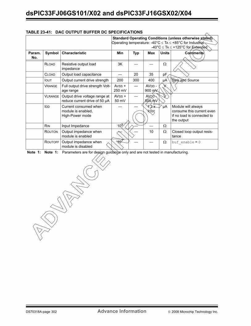
dsPIC33FJ06GS101/X02 and dsPIC33FJ16GSX02/X04
TABLE 23-41: DAC OUTPUT BUFFER DC SPECIFICATIONSStandard Operating Conditions (unless otherwise stated)
Operating temperature: -40°C ≤ TA ≤ +85°C for Industrial-40°C ≤ TA ≤ +125°C for Extended
Param. No.
Symbol Characteristic Min Typ Max Units Comments
RLOAD Resistive output load impedance
3K — — Ω
CLOAD Output load capacitance — 20 35 pFIOUT Output current drive strength 200 300 400 µA Sink and SourceVRANGE Full output drive strength Volt-
age rangeAVSS + 250 mV
— AVDD - 900 mV
V
VLRANGE Output drive voltage range at reduce current drive of 50 µA
AVSS + 50 mV
— AVDD - 500 mV
V
IDD Current consumed when module is enabled, High-Power mode
— — 1.3 x IOUT
µA Module will always consume this current even if no load is connected to the output
RIN Input Impedance 109 — — ΩROUTON Output impedance when
module is enabled— — 10 Ω Closed loop output resis-
tanceROUTOFF Output impedance when
module is disabled107 — — Ω buf_enable = 0
Note 1: Note 1: Parameters are for design guidance only and are not tested in manufacturing.
DS70318A-page 302 Advance Information © 2008 Microchip Technology Inc.

dsPIC33FJ06GS101/X02 and dsPIC33FJ16GSX02/X04
24.0 PACKAGING INFORMATION
Legend: XX...X Customer-specific informationY Year code (last digit of calendar year)YY Year code (last 2 digits of calendar year)WW Week code (week of January 1 is week ‘01’)NNN Alphanumeric traceability code Pb-free JEDEC designator for Matte Tin (Sn)* This package is Pb-free. The Pb-free JEDEC designator ( )
can be found on the outer packaging for this package.
Note: If the full Microchip part number cannot be marked on one line, it is carried over to the nextline, thus limiting the number of available characters for customer-specific information.
3e
3e
28-Lead SPDIP
XXXXXXXXXXXXXXXXXXXXXXXXXXXXXXXXXX
YYWWNNN
Example
dsPIC33FJ06GS
0730235
28-Lead SOIC
XXXXXXXXXXXXXXXXXXXXXXXXXXXXXXXXXXXXXXXXXXXXXXXXXXXXXXXXXXXX
YYWWNNN
Example
dsPIC33FJ06GS
0730235
202-E/SP
202-E/SO
3e
3e
18-Lead SOIC (.300”)
XXXXXXXXXXXXXXXXXXXXXXXXXXXXXXXXXXXX
YYWWNNN
Example
dsPIC33FJ06
0730235
GS101-I/SO3e
© 2008 Microchip Technology Inc. Advance Information DS70318A-page 303

dsPIC33FJ06GS101/X02 and dsPIC33FJ16GSX02/X04
24.1 Package Marking Information (Continued)
Legend: XX...X Customer-specific informationY Year code (last digit of calendar year)YY Year code (last 2 digits of calendar year)WW Week code (week of January 1 is week ‘01’)NNN Alphanumeric traceability code Pb-free JEDEC designator for Matte Tin (Sn)* This package is Pb-free. The Pb-free JEDEC designator ( )
can be found on the outer packaging for this package.
Note: If the full Microchip part number cannot be marked on one line, it is carried over to the nextline, thus limiting the number of available characters for customer-specific information.
3e
3e
28-Lead QFN-S
XXXXXXXXXXXXXXXXYYWWNNN
Example
33FJ06GS202EMM0730235
XXXXXXXXXX
44-Lead QFN
XXXXXXXXXXXXXXXXXXXX
YYWWNNN
dsPIC33FJ16
Example
GS504-E/ML0730235
44-Lead TQFP
XXXXXXXXXXXXXXXXXXXXXXXXXXXXXX
YYWWNNN
Example
dsPIC33FJ16GS504
0730235-E/PT
3e
3e
3e
DS70318A-page 304 Advance Information © 2008 Microchip Technology Inc.

dsPIC33FJ06GS101/X02 and dsPIC33FJ16GSX02/X04
24.2 Package Details
���������� ��������� ����������������������� !��"#$
%� ��&�� ������������� ����������������������������������� ������������������ �������� ���������������������������� � !��������!��� �"�� ���������� ����� ���������#���������$�� ���������#���������������������� �%��&����#���� ��'� !������������� �������������#���(�$"�)�'�&$�
*��+ *����!���������,����������������������������������������������-".+ -���������!������������������������������������������������#�#��������
%� �& .������������������#��/���� ��������#������������$�������#����/�������#������������������ �������#+00������������#����0#��/�����
1��� $2332$","-�!��������3���� $24 45$ $(6
4����������� 4 �7����� � ���8�*��5�������9����� ( : : ��;&$�� � ����/����,���/�� (� ��%& : :���� ������ (� %��% : %� %5�������<� �� " �%� %�*��$�� � ����/����<� �� "� 8�&%�*��5�������3����� ! �8�=%�*����������>�#������? � %��& : %�8&.����3����� 3 %�'% : ���8.���#���� 3� ��'%�-"..����(�����,�# � %@ : 7@3�� �,���/�� � %��7 : %� 3�� �<� �� � %� � : %�&�$�� �!�����(�����,�# � &@ : �&@$�� �!�����(�����*����� � &@ : �&@
c
hh
LL1
A2
A1
A
NOTE 1
1 2 3
be
EE1
D
φ
β
α
N
$�������# ,��������� !������ �%'A%&�*
© 2008 Microchip Technology Inc. Advance Information DS70318A-page 305
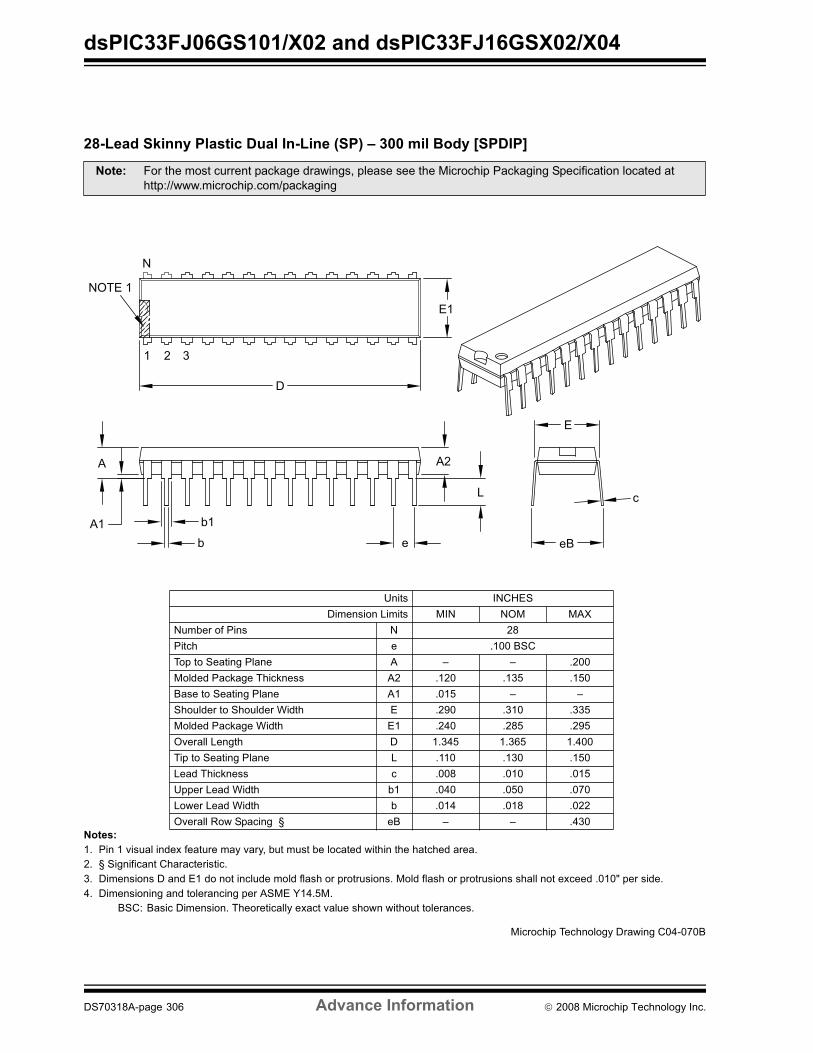
dsPIC33FJ06GS101/X02 and dsPIC33FJ16GSX02/X04
��������'��� ��� ��(���"����������)�������� !�("$
%� ��&�� ������������� ����������������������������������� ������������������ �������� ���������������������������� � !��������!��� �"�� ���������� ����� ���������#���������$�� ���������#���������������������� ��%�%B�#���� ��'� !������������� �������������#���(�$"�)�'�&$�
*��+ *����!���������,����������������������������������������������
%� �& .������������������#��/���� ��������#������������$�������#����/�������#������������������ �������#+00������������#����0#��/�����
1��� 24�9"�!��������3���� $24 45$ $(6
4����������� 4 �7����� � ��%%�*��,�#����������������� ( : : ��%%$�� � ����/����,���/�� (� ���% �� & ��&%*������������������� (� �%�& : :���� ���������� ���<� �� " ��=% � �% � &$�� � ����/����<� �� "� ��'% ��7& ��=&5�������3����� ! �� '& �� ;& ��'%%,�#����������������� 3 ���% �� % ��&%3�� �,���/�� � �%%7 �%�% �%�&1##���3�� �<� �� �� �%'% �%&% �%8%3�����3�� �<� �� � �%�' �%�7 �%��5�������-����#�������� �* : : �' %
NOTE 1
N
1 2
D
E1
eB
c
E
L
A2
eb
b1A1
A
3
$�������# ,��������� !������ �%'A%8%*
DS70318A-page 306 Advance Information © 2008 Microchip Technology Inc.

dsPIC33FJ06GS101/X02 and dsPIC33FJ16GSX02/X04
���������� ��*���+�� �%�������'�,��--��././��0����� !*+%��$1� 2��3���#�� �� ���, 2
%� ��&�� ������������� ����������������������������������� ������������������ �������� ���/���������������� � � !������������� �������������#���(�$"�)�'�&$�
*��+ *����!���������,����������������������������������������������-".+ -���������!������������������������������������������������#�#��������
%� �& .������������������#��/���� ��������#������������$�������#����/�������#������������������ �������#+00������������#����0#��/�����
1��� $2332$","-�!��������3���� $24 45$ $(6
4����������� 4 �7����� � %�;&�*��5�������9����� ( %�7% %�=% ��%%���� ���� (� %�%% %�%� %�%&��������,���/�� ( %��%�-".5�������<� �� " ;�%%�*��"�#�� ��� �<� �� "� �;& �8% '�8%5�������3����� ! ;�%%�*��"�#�� ��� �3����� !� �;& �8% '�8%��������<� �� � %�� %� 7 %�' ��������3����� 3 %� % %�'% %�&%�������A��A"�#�� ��� C %��% : :
D
E
21
N
E2
EXPOSEDPAD
2
1
D2
N
e
b
K
LNOTE 1
A3
A
A1
TOP VIEW BOTTOM VIEW
$�������# ,��������� !������ �%'A��'*
© 2008 Microchip Technology Inc. Advance Information DS70318A-page 307

dsPIC33FJ06GS101/X02 and dsPIC33FJ16GSX02/X04
���������� ��*���+�� �%�������'�,��--��././��0����� !*+%��$1� 2��3���#�� �� ���, 2
%� �& .������������������#��/���� ��������#������������$�������#����/�������#������������������ �������#+00������������#����0#��/�����
DS70318A-page 308 Advance Information © 2008 Microchip Technology Inc.

dsPIC33FJ06GS101/X02 and dsPIC33FJ16GSX02/X04
33�������� ��*���+�� �%�������'�,��-����/������ !*+%$
%� ��&�� ������������� ����������������������������������� ������������������ �������� ���/���������������� � � !������������� �������������#���(�$"�)�'�&$�
*��+ *����!���������,����������������������������������������������-".+ -���������!������������������������������������������������#�#��������
%� �& .������������������#��/���� ��������#������������$�������#����/�������#������������������ �������#+00������������#����0#��/�����
1��� $2332$","-�!��������3���� $24 45$ $(6
4����������� 4 ''����� � %�;&�*��5�������9����� ( %�7% %�=% ��%%���� ���� (� %�%% %�%� %�%&��������,���/�� ( %��%�-".5�������<� �� " 7�%%�*��"�#�� ��� �<� �� "� ;� % ;�'& ;�7%5�������3����� ! 7�%%�*��"�#�� ��� �3����� !� ;� % ;�'& ;�7%��������<� �� � %��& %� % %� 7��������3����� 3 %� % %�'% %�&%�������A��A"�#�� ��� C %��% : :
D EXPOSEDPAD
D2
e
b
KL
E2
21
NNOTE 1
21
E
N
BOTTOM VIEWTOP VIEW
A3 A1
A
$�������# ,��������� !������ �%'A�% *
© 2008 Microchip Technology Inc. Advance Information DS70318A-page 309

dsPIC33FJ06GS101/X02 and dsPIC33FJ16GSX02/X04
33�������� ��*���+�� �%�������'�,��-����/������ !*+%$
%� �& .������������������#��/���� ��������#������������$�������#����/�������#������������������ �������#+00������������#����0#��/�����
DS70318A-page 310 Advance Information © 2008 Microchip Technology Inc.

dsPIC33FJ06GS101/X02 and dsPIC33FJ16GSX02/X04
33�������� ��42��*���+�� 5��'�4��6�/6�/6����� �������!4*+$
%� ��&�� ������������� ����������������������������������� ������������������ �������� �����������������������#������D��E����������� � !��������!���� �"�� ���������� ����� ���������#���������$�� ���������#���������������������� �%��&����#���� ��'� !������������� �������������#���(�$"�)�'�&$�
*��+ *����!���������,����������������������������������������������-".+ -���������!������������������������������������������������#�#��������
%� �& .������������������#��/���� ��������#������������$�������#����/�������#������������������ �������#+00������������#����0#��/�����
1��� $2332$","-�!��������3���� $24 45$ $(6
4��������3�� 4 ''3�� ������ � %�7%�*��5�������9����� ( : : ���%$�� � ����/����,���/�� (� %�=& ��%% ��%&���� ����� (� %�%& : %��&.����3����� 3 %�'& %�;% %�8&.���#���� 3� ��%%�-"..����(���� � %@ �&@ 8@5�������<� �� " ���%%�*��5�������3����� ! ���%%�*��$�� � ����/����<� �� "� �%�%%�*��$�� � ����/����3����� !� �%�%%�*��3�� �,���/�� � %�%= : %��%3�� �<� �� � %� % %� 8 %�'&$�� �!�����(�����,�# � ��@ ��@ � @$�� �!�����(�����*����� � ��@ ��@ � @
A
E
E1
DD1
e
b
NOTE 1NOTE 2
N
1 2 3
c
A1L
A2L1
α
φ
β
$�������# ,��������� !������ �%'A%8;*
© 2008 Microchip Technology Inc. Advance Information DS70318A-page 311

dsPIC33FJ06GS101/X02 and dsPIC33FJ16GSX02/X04
33�������� ��42��*���+�� 5��'�4��6�/6�/6����� �������!4*+$
%� �& .������������������#��/���� ��������#������������$�������#����/�������#������������������ �������#+00������������#����0#��/�����
DS70318A-page 312 Advance Information © 2008 Microchip Technology Inc.
dsPIC33FJ06GS101/X02 and dsPIC33FJ16GSX02/X04
APPENDIX A: REVISION HISTORYRevision A (January 2008)This is the initial revision of this document.
© 2008 Microchip Technology Inc. Advance Information DS70318A-page 313

dsPIC33FJ06GS101/X02 and dsPIC33FJ16GSX02/X04
NOTES:
DS70318A-page 314 Advance Information © 2008 Microchip Technology Inc.

dsPIC33FJ06GS101/X02 and dsPIC33FJ16GSX02/X04
INDEXNumerics10-bit High Speed Analog-to-Digital Converter. See A/D
AA/D .................................................................................... 227A/D Control Register (ADCON)......................................... 235A/D Convert Pair Control Register 0 (ADCPC0) ............... 239A/D Convert Pair Control Register 1 (ADCPC1) ............... 241A/D Convert Pair Control Register 2 (ADCPC2) ............... 243A/D Convert Pair Control Register 3 (ADCPC3) ............... 245A/D Port Configuration Register (ADPCFG) ..................... 238A/D Status Register (ADSTAT)......................................... 237AC Characteristics ............................................................ 280
Internal RC Accuracy ................................................ 282Load Conditions ........................................................ 280
Alternate Vector Table (AIVT) ............................................. 83Arithmetic Logic Unit (ALU)................................................. 23Assembler
MPASM Assembler................................................... 268Automatic Clock Stretch.................................................... 211
Receive Mode ........................................................... 211Transmit Mode .......................................................... 211
BBarrel Shifter ....................................................................... 27Bit-Reversed Addressing .................................................... 62
Example ...................................................................... 63Implementation ........................................................... 62Sequence Table (16-Entry)......................................... 63
Block Diagrams16-bit Timer1 Module ................................................ 165Connections for On-Chip Voltage Regulator............. 254Device Clock ............................................................. 123DSP Engine ................................................................ 24dsPIC33FJ06GS101/X02 and dsPIC33FJ16GSX02/X04
CPU Core ........................................................... 18Input Capture ............................................................ 173Output Compare ....................................................... 175PLL............................................................................ 125Reset System.............................................................. 75Shared Port Structure ............................................... 136SPI ............................................................................ 202Timer2 (16-bit) .......................................................... 167Timer2/3 (32-bit) ....................................................... 169UART ........................................................................ 219Watchdog Timer (WDT) ............................................ 255
CC Compilers
MPLAB C18 .............................................................. 268MPLAB C30 .............................................................. 268
Clock Switching................................................................. 132Enabling .................................................................... 132Sequence.................................................................. 132
Code ExamplesErasing a Program Memory Page............................... 73Initiating a Programming Sequence............................ 74Loading Write Buffers ................................................. 74Port Write/Read ........................................................ 137PWRSAV Instruction Syntax..................................... 133
Code Protection ........................................................ 251, 257Comparator Control Register (CMPCONx) ....................... 249Comparator DAC Control Register (CMPDACx)............... 250
Configuration Bits ............................................................. 251Configuration Register Map.............................................. 251Configuring Analog Port Pins............................................ 137CPU
Control Register.......................................................... 20CPU Clocking System ...................................................... 124
PLL Configuration..................................................... 125Selection................................................................... 124Sources .................................................................... 124
Customer Change Notification Service............................. 319Customer Notification Service .......................................... 319Customer Support............................................................. 319
DData Accumulators and Adder/Subtracter .......................... 25
Data Space Write Saturation ...................................... 27Overflow and Saturation ............................................. 25Round Logic ............................................................... 26Write Back .................................................................. 26
Data Address Space........................................................... 31Alignment.................................................................... 31Memory Map for dsPIC33FJ06GS101/102Devices with 256 KBs RAM........................................ 32Memory Map for dsPIC33FJ06GS202 Device with 1 KB RAM .......................................................... 33Memory Map for dsPIC33FJ16GS402/404/502/504 Devices with 2 KBs RAM............................................ 34Near Data Space ........................................................ 31Software Stack ........................................................... 59Width .......................................................................... 31
DC Characteristics............................................................ 272I/O Pin Input Specifications ...................................... 277I/O Pin Output Specifications.................................... 278Idle Current (IDOZE) .................................................. 276Idle Current (IIDLE) .................................................... 275Operating Current (IDD) ............................................ 274Power-Down Current (IPD)........................................ 276Program Memory...................................................... 279Temperature and Voltage Specifications.................. 273
Development Support ....................................................... 267Doze Mode ....................................................................... 134DSP Engine ........................................................................ 23
Multiplier ..................................................................... 25dsPIC33FJ06GS101........................................................... 14
EElectrical Characteristics .................................................. 271
AC Characteristics and Timing Parameters ............. 280Errata.................................................................................. 12
FFail-Safe Clock Monitor .................................................... 132Flash Program Memory ...................................................... 69
Control Registers........................................................ 70Operations .................................................................. 70Programming Algorithm.............................................. 73RTSP Operation ......................................................... 70Table Instructions ....................................................... 69
Flexible Configuration....................................................... 251
HHigh-Speed PWM............................................................. 179
© 2008 Microchip Technology Inc. Advance Information DS70318A-page 315

dsPIC33FJ06GS101/X02 and dsPIC33FJ16GSX02/X04
II/O Ports ............................................................................ 135
Parallel I/O (PIO)....................................................... 135Write/Read Timing .................................................... 137
I2CAddresses ................................................................. 211Baud Rate Generator ................................................ 209General Call Address Support .................................. 211Interrupts................................................................... 209IPMI Support ............................................................. 211Master Mode Operation
Clock Arbitration................................................ 212Multi-Master Communication, Bus Collision and
Bus Arbitration .......................................... 212Operating Modes ...................................................... 209Registers................................................................... 209Slave Address Masking ............................................ 211Slope Control ............................................................ 212Software Controlled Clock Stretching (STREN = 1).. 211
In-Circuit Debugger ........................................................... 256In-Circuit Emulation........................................................... 251In-Circuit Serial Programming (ICSP) ....................... 251, 256Infrared Support
External IrDA, IrDA Clock Output.............................. 221Input Capture .................................................................... 173
Registers................................................................... 174Input Change Notification.................................................. 137Instruction Addressing Modes............................................. 59
File Register Instructions ............................................ 59Fundamental Modes Supported.................................. 60MAC Instructions......................................................... 60MCU Instructions ........................................................ 59Move and Accumulator Instructions............................ 60Other Instructions........................................................ 60
Instruction SetOverview ................................................................... 262Summary................................................................... 259
Instruction-Based Power-Saving Modes ........................... 133Idle ............................................................................ 134Sleep......................................................................... 133
Interfacing Program and Data Memory Spaces .................. 64Internal RC Oscillator
Use with WDT ........................................................... 255Internet Address................................................................ 319Interrupt Control and Status Registers................................ 87
IECx ............................................................................ 87IFSx............................................................................. 87INTCON1 .................................................................... 87INTCON2 .................................................................... 87IPCx ............................................................................ 87
Interrupt Setup Procedures ............................................... 121Initialization ............................................................... 121Interrupt Disable........................................................ 121Interrupt Service Routine .......................................... 121Trap Service Routine ................................................ 121
Interrupt Vector Table (IVT) ................................................ 83Interrupts Coincident with Power Save Instructions.......... 134
JJTAG Boundary Scan Interface ........................................ 251JTAG Interface .................................................................. 256
LLeading-Edge Blanking Control Register (LEBCONx) ...... 198
MMemory Organization ......................................................... 29Microchip Internet Web Site.............................................. 319Modulo Addressing ............................................................. 61
Applicability................................................................. 62Operation Example..................................................... 61Start and End Address ............................................... 61W Address Register Selection.................................... 61
MPLAB ASM30 Assembler, Linker, Librarian ................... 268MPLAB ICD 2 In-Circuit Debugger ................................... 269MPLAB ICE 2000 High-Performance Universal In-Circuit Emulator ............................................................ 269MPLAB Integrated Development Environment Software ...................................................... 267MPLAB PM3 Device Programmer .................................... 269MPLAB REAL ICE In-Circuit Emulator System ................ 269MPLINK Object Linker/MPLIB Object Librarian ................ 268
OOpen-Drain Configuration................................................. 137Oscillator Configuration .................................................... 123Output Compare ............................................................... 175
PPackaging ......................................................................... 303
18-Lead SOIC........................................................... 30528-Lead QFN-S ........................................................ 30728-Lead QFN-S Land Pattern................................... 30828-Lead SPDIP......................................................... 30644-Lead QFN............................................................ 30944-Lead QFN Land Pattern ...................................... 31044-Lead TQFP.......................................................... 31144-Lead TQFP Land Pattern .................................... 312Marking..................................................................... 303
Peripheral Module Disable (PMD) .................................... 134PICSTART Plus Development Programmer..................... 270Pinout I/O Descriptions (table)............................................ 15PLL Block Diagram ........................................................... 125Power-on Reset (POR)....................................................... 80Power-Saving Features .................................................... 133
Clock Frequency and Switching ............................... 133Primary PWM Time Base Capture Register (PWMCAPx) 199Program Address Space..................................................... 29
Construction ............................................................... 64Data Access from Program Memory Using Program Space Visibility................................... 67Data Access from Program Memory Using Table Instructions ............................................. 66Data Access from, Address Generation ..................... 65Memory Map............................................................... 29Table Read Instructions
TBLRDH ............................................................. 66TBLRDL.............................................................. 66
Visibility Operation...................................................... 67Program Memory
Interrupt Vector ........................................................... 30Organization ............................................................... 30Reset Vector ............................................................... 30
PWM Alternate Dead Time Register (ALTDTRx) ............. 191PWM Control Register (PWMCONx) ................................ 186PWM Dead Time Register (DTRx) ................................... 191PWM Fault Current-Limit Control Register (FCLCONx) ... 195PWM I/O Control Register (IOCONx) ............................... 193PWM Master Duty Cycle Register (MDC)......................... 185PWM Time Base Control Register (PTCON).................... 182
DS70318A-page 316 Advance Information © 2008 Microchip Technology Inc.

dsPIC33FJ06GS101/X02 and dsPIC33FJ16GSX02/X04
PWM Trigger Compare Value Register (TRIGx)............... 197
RReader Response ............................................................. 320Registers
ADCON..................................................................... 235ADCPC0 ................................................................... 239ADCPC1 ................................................................... 241ADCPC2 ................................................................... 243ADCPC3 ................................................................... 245ADPCFG ................................................................... 238ADSTAT.................................................................... 237ALTDTRx .................................................................. 191CLKDIV (Clock Divisor)............................................. 127CMPCONx ................................................................ 249CMPDACx................................................................. 250CORCON (Core Control) ............................................ 22DTRx......................................................................... 191FCLCONx ................................................................. 195I2CxCON (I2Cx Control) ........................................... 213I2CxMSK (I2Cx Slave Mode Address Mask) ............ 217I2CxSTAT (I2Cx Status) ........................................... 215ICxCON (Input Capture x Control) ............................ 174IEC0 (Interrupt Enable Control Register 0) ................. 99IEC1 (Interrupt Enable Control Register 1) ............... 101IEC3 (Interrupt Enable Control Register 3) ............... 102IEC4 (Interrupt Enable Control Register 4) ............... 102IEC5 (Interrupt Enable Control Register 5) ............... 103IFS0 (Interrupt Flag Status Register 0) ....................... 92IFS1 (Interrupt Flag Status Register 1) ....................... 94IFS3 (Interrupt Flag Status Register 3) ....................... 95IFS4 (Interrupt Flag Status Register 4) ....................... 95IFS5 (Interrupt Flag Status Register 5) ....................... 96IFS6 (Interrupt Flag Status Register 6) ............... 97, 104IFS7 (Interrupt Flag Status Register 7) ............... 98, 105INTCON1 (Interrupt Control Register 1) ..................... 89INTTREG Interrupt Control and Status Register....... 120IOCONx .................................................................... 193IPC0 (Interrupt Priority Control Register 0) ............... 106IPC1 (Interrupt Priority Control Register 1) ............... 107IPC14 (Interrupt Priority Control Register 14) ........... 112IPC16 (Interrupt Priority Control Register 16) ........... 112IPC2 (Interrupt Priority Control Register 2) ............... 108IPC23 (Interrupt Priority Control Register 23) ........... 113IPC24 (Interrupt Priority Control Register 24) ........... 114IPC25 (Interrupt Priority Control Register 25) ........... 115IPC26 (Interrupt Priority Control Register 26) ........... 116IPC27 (Interrupt Priority Control Register 27) ........... 117IPC28 (Interrupt Priority Control Register 28) ........... 118IPC29 (Interrupt Priority Control Register 29) ........... 119IPC3 (Interrupt Priority Control Register 3) ............... 109IPC4 (Interrupt Priority Control Register 4) ............... 110IPC5 (Interrupt Priority Control Register 5) ............... 111IPC7 (Interrupt Priority Control Register 7) ............... 111LEBCONx ................................................................. 198MDC.......................................................................... 185NVMCON (Flash Memory Control) ............................. 71NVMKEY (Nonvolatile Memory Key) .......................... 72OCxCON (Output Compare x Control) ..................... 177OSCCON (Oscillator Control) ................................... 126PLLFBD (PLL Feedback Divisor).............................. 128PTCON ..................................................................... 182PWMCAPx ................................................................ 199PWMCONx ............................................................... 186RCON (Reset Control) ................................................ 76SEVTCMP................................................................. 185
SPIxCON1 (SPIx Control 1) ..................................... 206SPIxCON2 (SPIx Control 2) ..................................... 208SPIxSTAT (SPIx Status and Control) ....................... 205SR (CPU Status) .................................................. 20, 88T1CON (Timer1 Control) .......................................... 166TRIGx ....................................................................... 197TxCON (Type B Time Base Control) ........................ 170TyCON (Type C Time Base Control)........................ 171UxMODE (UARTx Mode) ......................................... 222UxSTA (UARTx Status and Control) ........................ 224
ResetIllegal Opcode....................................................... 75, 82Trap Conflict ......................................................... 81, 82Uninitialized W Register ....................................... 75, 82
Reset Sequence ................................................................. 83Resets ................................................................................ 75
SSerial Peripheral Interface (SPI) ....................................... 201Software Reset Instruction (SWR)...................................... 81Software Simulator (MPLAB SIM) .................................... 268Software Stack Pointer, Frame Pointer
CALLL Stack Frame ................................................... 59Special Event Compare Register (SEVTCMP)................. 185Special Features of the CPU ............................................ 251SPI
Master, Frame Master Connection ........................... 203Master/Slave Connection ......................................... 203Slave, Frame Master Connection ............................. 204Slave, Frame Slave Connection ............................... 204
Symbols Used in Opcode Descriptions ............................ 260
TTemperature and Voltage Specifications
AC............................................................................. 280Timer1 .............................................................................. 165Timer2/3 ........................................................................... 167Timing Characteristics
A/D Conversion10-Bit High-Speed (CHPS = 01, SIMSAM = 0,
ASAM = 0, SSRC = 000).......................... 300CLKO and I/O ........................................................... 283
Timing DiagramsBrown-out Situations .................................................. 81External Clock .......................................................... 281I2Cx Bus Data (Master Mode) .................................. 295I2Cx Bus Data (Slave Mode) .................................... 297I2Cx Bus Start/Stop Bits (Master Mode)................... 295I2Cx Bus Start/Stop Bits (Slave Mode)..................... 297Input Capture (CAPx) ............................................... 287Motor Control PWM .................................................. 289Motor Control PWM Fault ......................................... 289OC/PWM .................................................................. 288Output Compare (OCx) ............................................ 287Reset, Watchdog Timer, Oscillator Start-up Timer and
Power-up Timer ................................................ 284SPIx Master Mode (CKE = 0) ................................... 290SPIx Master Mode (CKE = 1) ................................... 291SPIx Slave Mode (CKE = 0) ..................................... 292SPIx Slave Mode (CKE = 1) ..................................... 293Timer1, 2, 3 External Clock ...................................... 285
Timing RequirementsCLKO and I/O ........................................................... 283External Clock .......................................................... 281Input Capture............................................................ 287
Timing Specifications
© 2008 Microchip Technology Inc. Advance Information DS70318A-page 317

dsPIC33FJ06GS101/X02 and dsPIC33FJ16GSX02/X04
10-bit A/D Conversion Requirements ....................... 300I2Cx Bus Data Requirements (Master Mode) ........... 296I2Cx Bus Data Requirements (Slave Mode) ............. 298Motor Control PWM Requirements ........................... 289Output Compare Requirements ................................ 287PLL Clock.................................................................. 282Reset, Watchdog Timer, Oscillator Start-upTimer, Power-up Timer and Brown-out Reset Requirements ................................................. 284Simple OC/PWM Mode Requirements ..................... 288SPIx Master Mode (CKE = 0) Requirements ............ 290SPIx Master Mode (CKE = 1) Requirements ............ 291SPIx Slave Mode (CKE = 0) Requirements .............. 292SPIx Slave Mode (CKE = 1) Requirements .............. 294Timer1 External Clock Requirements ....................... 285Timer2 External Clock Requirements ....................... 286Timer3 External Clock Requirements ....................... 286
UUART
Baud RateGenerator (BRG)............................................... 220
Break and Sync Transmit Sequence ........................ 221Flow Control Using UxCTS and UxRTS Pins............ 221Receiving in 8-bit or 9-bit Data Mode........................ 221Transmitting in 8-bit Data Mode................................ 221Transmitting in 9-bit Data Mode................................ 221
Universal Asynchronous Receiver Transmitter (UART).... 219Using the RCON Status Bits ............................................... 82
VVoltage Regulator (On-Chip)............................................. 254
WWatchdog Time-out Reset (WDTR) .................................... 81Watchdog Timer (WDT) ............................................ 251, 255
Programming Considerations ................................... 255WWW Address.................................................................. 319WWW, On-Line Support...................................................... 12
DS70318A-page 318 Advance Information © 2008 Microchip Technology Inc.

dsPIC33FJ06GS101/X02 and dsPIC33FJ16GSX02/X04
THE MICROCHIP WEB SITEMicrochip provides online support via our WWW site atwww.microchip.com. This web site is used as a meansto make files and information easily available tocustomers. Accessible by using your favorite Internetbrowser, the web site contains the followinginformation:
• Product Support – Data sheets and errata, application notes and sample programs, design resources, user’s guides and hardware support documents, latest software releases and archived software.
• General Technical Support – Frequently Asked Questions (FAQ), technical support requests, online discussion groups, Microchip consultant program member listing.
• Business of Microchip – Product selector and ordering guides, latest Microchip press releases, listing of seminars and events, listings of Microchip sales offices, distributors and factory representatives.
CUSTOMER CHANGE NOTIFICATION SERVICEMicrochip’s customer notification service helps keepcustomers current on Microchip products. Subscriberswill receive e-mail notification whenever there arechanges, updates, revisions or errata related to aspecified product family or development tool of interest.
To register, access the Microchip web site atwww.microchip.com, click on Customer ChangeNotification and follow the registration instructions.
CUSTOMER SUPPORTUsers of Microchip products can receive assistancethrough several channels:
• Distributor or Representative• Local Sales Office• Field Application Engineer (FAE)• Technical Support
Customers should contact their distributor,representative or field application engineer (FAE) forsupport. Local sales offices are also available to helpcustomers. A listing of sales offices and locations isincluded in the back of this document.
Technical support is available through the web siteat: http://support.microchip.com
© 2008 Microchip Technology Inc. Advance Information DS70318A-page 319

dsPIC33FJ06GS101/X02 and dsPIC33FJ16GSX02/X04
READER RESPONSEIt is our intention to provide you with the best documentation possible to ensure successful use of your Microchipproduct. If you wish to provide your comments on organization, clarity, subject matter, and ways in which ourdocumentation can better serve you, please FAX your comments to the Technical Publications Managerat (480) 792-4150.
Please list the following information, and use this outline to provide us with your comments about this document.
To: Technical Publications Manager
RE: Reader ResponseTotal Pages Sent ________
From: Name
CompanyAddressCity / State / ZIP / Country
Telephone: (_______) _________ - _________
Application (optional):
Would you like a reply? Y N
Device: Literature Number:
Questions:
FAX: (______) _________ - _________
DS70318AdsPIC33FJ06GS101/X02 and dsPIC33FJ16GSX02/X04
1. What are the best features of this document?
2. How does this document meet your hardware and software development needs?
3. Do you find the organization of this document easy to follow? If not, why?
4. What additions to the document do you think would enhance the structure and subject?
5. What deletions from the document could be made without affecting the overall usefulness?
6. Is there any incorrect or misleading information (what and where)?
7. How would you improve this document?
DS70318A-page 320 Advance Information © 2008 Microchip Technology Inc.

© 2008 Microchip Technology Inc. Advance Information DS70318A-page 321
dsPIC33FJ06GS101/X02 and dsPIC33FJ16GSX02/X04
PRODUCT IDENTIFICATION SYSTEMTo order or obtain information, e.g., on pricing or delivery, refer to the factory or the listed sales office.
Architecture: 33 = 16-bit Digital Signal Controller
Flash Memory Family: FJ = Flash program memory, 3.3V
Product Group: GS1 = Switch Mode Power Supply (SMPS) familyGS2 = Switch Mode Power Supply (SMPS) familyGS4 = Switch Mode Power Supply (SMPS) familyGS5 = Switch Mode Power Supply (SMPS) family
Pin Count: 01 = 18-pin02 = 28-pin04 = 44-pin
Temperature Range: I = -40°C to+85°C (Industrial)E = -40°C to+125°C (Extended)
Package: SO = Plastic Small Outline - Wide - 7.50 mm body (SOIC)SP = Skinny Plastic Dual In-Line - 300 mil body (SPDIP)ML = Plastic Quad Flat, No Lead Package - 8x8 mm body (QFN)MM = Plastic Quad Flat, No Lead Package - 6x6x0.9 mm body (QFN-S)PT = Plastic Thin Quad Flatpack - 10x10x1 mm body (TQFP)
Examples:a) dsPIC33FJ06GS102-E/SP:
SMPS dsPIC33, 6 KB program memory, 28-pin, Extended temp.,SPDIP package.
Microchip TrademarkArchitectureFlash Memory FamilyProgram Memory Size (KB)Product GroupPin Count
Temperature RangePackagePattern
dsPIC 33 FJ 06 GS1 02 T E / SP - XXX
Tape and Reel Flag (if applicable)

DS70318A-page 322 Advance Information © 2008 Microchip Technology Inc.
AMERICASCorporate Office2355 West Chandler Blvd.Chandler, AZ 85224-6199Tel: 480-792-7200 Fax: 480-792-7277Technical Support: http://support.microchip.comWeb Address: www.microchip.comAtlantaDuluth, GA Tel: 678-957-9614 Fax: 678-957-1455BostonWestborough, MA Tel: 774-760-0087 Fax: 774-760-0088ChicagoItasca, IL Tel: 630-285-0071 Fax: 630-285-0075DallasAddison, TX Tel: 972-818-7423 Fax: 972-818-2924DetroitFarmington Hills, MI Tel: 248-538-2250Fax: 248-538-2260KokomoKokomo, IN Tel: 765-864-8360Fax: 765-864-8387Los AngelesMission Viejo, CA Tel: 949-462-9523 Fax: 949-462-9608Santa ClaraSanta Clara, CA Tel: 408-961-6444Fax: 408-961-6445TorontoMississauga, Ontario, CanadaTel: 905-673-0699 Fax: 905-673-6509
ASIA/PACIFICAsia Pacific OfficeSuites 3707-14, 37th FloorTower 6, The GatewayHarbour City, KowloonHong KongTel: 852-2401-1200Fax: 852-2401-3431Australia - SydneyTel: 61-2-9868-6733Fax: 61-2-9868-6755China - BeijingTel: 86-10-8528-2100 Fax: 86-10-8528-2104China - ChengduTel: 86-28-8665-5511Fax: 86-28-8665-7889China - Hong Kong SARTel: 852-2401-1200 Fax: 852-2401-3431China - NanjingTel: 86-25-8473-2460Fax: 86-25-8473-2470China - QingdaoTel: 86-532-8502-7355Fax: 86-532-8502-7205China - ShanghaiTel: 86-21-5407-5533 Fax: 86-21-5407-5066China - ShenyangTel: 86-24-2334-2829Fax: 86-24-2334-2393China - ShenzhenTel: 86-755-8203-2660 Fax: 86-755-8203-1760China - WuhanTel: 86-27-5980-5300Fax: 86-27-5980-5118China - XiamenTel: 86-592-2388138 Fax: 86-592-2388130China - XianTel: 86-29-8833-7252Fax: 86-29-8833-7256China - ZhuhaiTel: 86-756-3210040 Fax: 86-756-3210049
ASIA/PACIFICIndia - BangaloreTel: 91-80-4182-8400 Fax: 91-80-4182-8422India - New DelhiTel: 91-11-4160-8631Fax: 91-11-4160-8632India - PuneTel: 91-20-2566-1512Fax: 91-20-2566-1513Japan - YokohamaTel: 81-45-471- 6166 Fax: 81-45-471-6122Korea - DaeguTel: 82-53-744-4301Fax: 82-53-744-4302Korea - SeoulTel: 82-2-554-7200Fax: 82-2-558-5932 or 82-2-558-5934Malaysia - Kuala LumpurTel: 60-3-6201-9857Fax: 60-3-6201-9859Malaysia - PenangTel: 60-4-227-8870Fax: 60-4-227-4068Philippines - ManilaTel: 63-2-634-9065Fax: 63-2-634-9069SingaporeTel: 65-6334-8870Fax: 65-6334-8850Taiwan - Hsin ChuTel: 886-3-572-9526Fax: 886-3-572-6459Taiwan - KaohsiungTel: 886-7-536-4818Fax: 886-7-536-4803Taiwan - TaipeiTel: 886-2-2500-6610 Fax: 886-2-2508-0102Thailand - BangkokTel: 66-2-694-1351Fax: 66-2-694-1350
EUROPEAustria - WelsTel: 43-7242-2244-39Fax: 43-7242-2244-393Denmark - CopenhagenTel: 45-4450-2828 Fax: 45-4485-2829France - ParisTel: 33-1-69-53-63-20 Fax: 33-1-69-30-90-79Germany - MunichTel: 49-89-627-144-0 Fax: 49-89-627-144-44Italy - Milan Tel: 39-0331-742611 Fax: 39-0331-466781Netherlands - DrunenTel: 31-416-690399 Fax: 31-416-690340Spain - MadridTel: 34-91-708-08-90Fax: 34-91-708-08-91UK - WokinghamTel: 44-118-921-5869Fax: 44-118-921-5820
WORLDWIDE SALES AND SERVICE
01/02/08