

High-Output-Drive Operational Amplifier With Shutdown (Rev. D)
25
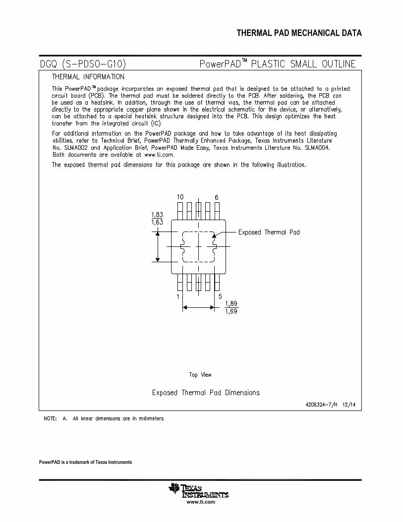
1FEATURES 1 2 3 4 8 7 6 5 1OUT 1IN- 1IN+ GND V DD 2OUT 2IN- 2IN+ TLV4112 D OR DGN PACKAGE (TOP VIEW) P0029-01 DESCRIPTION TLV4110-EP, TLV4111-EP TLV4112-EP, TLV4113-EP www.ti.com............................................................................................................................................................... SGLS314D –JUNE 2006–REVISED MAY 2008 HIGH-OUTPUT-DRIVE OPERATIONAL AMPLIFIERS WITH SHUTDOWN 23• Controlled Baseline – One Assembly Site – One Test Site – One Fabrication Site • Extended Temperature Performance of –55°C to 125°C • Enhanced Diminishing Manufacturing Sources (DMS) Support • Enhanced Product-Change Notification • Qualification Pedigree (1) The TLV411x single-supply operational amplifiers • High Output Drive . . . >300 mA provide output currents in excess of 300 mA at 5 V. This enables standard pin-out amplifiers to be used • Rail-To-Rail Output as high current buffers or in coil driver applications. • Unity-Gain Bandwidth . . . 2.7 MHz The TLV4110 and TLV4113 come with a shutdown • Slew Rate . . . 1.5 V/μs feature. • Supply Current . . . 700 μA/Per Channel The TLV411x is available in the ultra-small MSOP • Supply Voltage Range . . . 2.5 V to 6 V PowerPAD™ package, which offers the exceptional thermal impedance required for amplifiers delivering • Universal Op Amp EVM high current levels. (1) Component qualification in accordance with JEDEC and industry standards to ensure reliable operation over an All TLV411x devices are offered in SOIC (single and extended temperature range. This includes, but is not limited dual) and MSOP PowerPAD (dual). to, Highly Accelerated Stress Test (HAST) or biased 85/85, temperature cycle, autoclave or unbiased HAST, electromigration, bond intermetallic life, and mold compound life. Such qualification testing should not be viewed as justifying use of this component beyond specified performance and environmental limits. FAMILY PACKAGE TABLE PACKAGE TYPES NUMBER OF DEVICE SHUTDOWN UNIVERSAL EVM BOARD CHANNELS MSOP SOIC TLV4110 1 8 8 Yes TLV4111 1 8 8 – See the EVM Selection Guide (SLOU060) TLV4112 2 8 8 – TLV4113 2 10 14 Yes 1 Please be aware that an important notice concerning availability, standard warranty, and use in critical applications of Texas Instruments semiconductor products and disclaimers thereto appears at the end of this data sheet. 2PowerPAD is a trademark of Texas Instruments. 3Parts, Microsim PSpice are trademarks of MicroSim Corporation. PRODUCTION DATA information is current as of publication date. Copyright © 2006–2008, Texas Instruments Incorporated Products conform to specifications per the terms of the Texas Instruments standard warranty. Production processing does not necessarily include testing of all parameters.
Transcript of High-Output-Drive Operational Amplifier With Shutdown (Rev. D)

1FEATURES
1
2
3
4
8
7
6
5
1OUT1IN−1IN+GND
VDD
2OUT2IN−2IN+
TLV4112D OR DGN PACKAGE
(TOP VIEW)
P0029-01
DESCRIPTION
TLV4110-EP, TLV4111-EPTLV4112-EP, TLV4113-EP
www.ti.com............................................................................................................................................................... SGLS314D–JUNE 2006–REVISED MAY 2008
HIGH-OUTPUT-DRIVE OPERATIONAL AMPLIFIERSWITH SHUTDOWN
23• Controlled Baseline– One Assembly Site– One Test Site– One Fabrication Site
• Extended Temperature Performance of–55°C to 125°C
• Enhanced Diminishing Manufacturing Sources(DMS) Support
• Enhanced Product-Change Notification• Qualification Pedigree (1)
The TLV411x single-supply operational amplifiers• High Output Drive . . . >300 mA provide output currents in excess of 300 mA at 5 V.
This enables standard pin-out amplifiers to be used• Rail-To-Rail Outputas high current buffers or in coil driver applications.• Unity-Gain Bandwidth . . . 2.7 MHz The TLV4110 and TLV4113 come with a shutdown
• Slew Rate . . . 1.5 V/µs feature.• Supply Current . . . 700 µA/Per Channel The TLV411x is available in the ultra-small MSOP• Supply Voltage Range . . . 2.5 V to 6 V PowerPAD™ package, which offers the exceptional
thermal impedance required for amplifiers delivering• Universal Op Amp EVMhigh current levels.(1) Component qualification in accordance with JEDEC and
industry standards to ensure reliable operation over an All TLV411x devices are offered in SOIC (single andextended temperature range. This includes, but is not limited dual) and MSOP PowerPAD (dual).to, Highly Accelerated Stress Test (HAST) or biased 85/85,temperature cycle, autoclave or unbiased HAST,electromigration, bond intermetallic life, and mold compoundlife. Such qualification testing should not be viewed asjustifying use of this component beyond specifiedperformance and environmental limits.
FAMILY PACKAGE TABLEPACKAGE TYPESNUMBER OFDEVICE SHUTDOWN UNIVERSAL EVM BOARDCHANNELS MSOP SOIC
TLV4110 1 8 8 YesTLV4111 1 8 8 –
See the EVM Selection Guide (SLOU060)TLV4112 2 8 8 –TLV4113 2 10 14 Yes
1
Please be aware that an important notice concerning availability, standard warranty, and use in critical applications ofTexas Instruments semiconductor products and disclaimers thereto appears at the end of this data sheet.
2PowerPAD is a trademark of Texas Instruments.3Parts, Microsim PSpice are trademarks of MicroSim Corporation.
PRODUCTION DATA information is current as of publication date. Copyright © 2006–2008, Texas Instruments IncorporatedProducts conform to specifications per the terms of the TexasInstruments standard warranty. Production processing does notnecessarily include testing of all parameters.

IOH − High-Level Output Current − mA
2.0
2.1
2.2
2.3
2.4
2.5
2.6
2.7
2.8
2.9
3.0
0 50 100 150 200 250 300
VO
H −
Hig
h-Le
vel O
utpu
t Vol
tage
− V
G004
VDD = 3 V
TA = 70C
TA = 25C
TA = 0C
TA = −40C
TA = 125C
IOL − Low-Level Output Current − mA
0.0
0.1
0.2
0.3
0.4
0.5
0.6
0.7
0.8
0.9
1.0
0 50 100 150 200 250 300
VO
L −
Low
-Lev
el O
utpu
t Vol
tage
− V
G005
VDD = 3 VTA = 70C
TA = 25C
TA = −40C
TA = 0C
TA = 125C
TLV4110-EP, TLV4111-EPTLV4112-EP, TLV4113-EPSGLS314D–JUNE 2006–REVISED MAY 2008............................................................................................................................................................... www.ti.com
TLV4110 AND TLV4111 AVAILABLE OPTIONSTA PACKAGED DEVICES
MSOPSMALL OUTLINE (D) (1) (2) SMALL OUTLINE SYMBOL(DGN) (1)
TLV4110MDREP (3) TLV4110MDGNREP (3) BTB–55°C to 125°C
TLV4111MDREP (3) TLV4111MDGNREP (3) BTC
(1) The R designation indicates package is taped and reeled.(2) In the SOIC package, the maximum RMS output power is thermally limited to 350 mW; 700 mW peaks can be driven, as long as the
RMS value is less than 350 mW.(3) Product preview.
TLV4112 AND TLV4113 AVAILABLE OPTIONSPACKAGED DEVICES
MSOPTA SMALL OUTLINESMALL OUTLINE SMALL OUTLINE(D) (1) (2) SYMBOL SYMBOL(DGN) (1) (DGQ) (1)
TLV4112MDREP (3) TLV4112MDGNREP (3) BTD – ––55°C to 125°C
TLV4113MDREP (3) – – TLV4113MDGQREP BTE
(1) The R designation indicates package is taped and reeled.(2) In the SOIC package, the maximum RMS output power is thermally limited to 350 mW; 700 mW peaks can be driven, as long as the
RMS value is less than 350 mW.(3) Product preview.
2 Submit Documentation Feedback Copyright © 2006–2008, Texas Instruments Incorporated
Product Folder Link(s): TLV4110-EP, TLV4111-EP TLV4112-EP, TLV4113-EP

TLV411X PACKAGE PINOUTS
1
2
3
4
5
6
7
14
13
12
11
10
9
8
1OUT1IN−1IN+GND
NC1SHDN
NC
VDD
2OUT2IN−2IN+NC2SHDNNC
(TOP VIEW)
1
2
3
4
8
7
6
5
NCIN−IN+
GND
SHDNVDDOUTNC
TLV4110D OR DGN PACKAGE
(TOP VIEW)
1
2
3
4
8
7
6
5
1OUT1IN−1IN+GND
VDD
2OUT2IN−2IN+
TLV4112D OR DGN PACKAGE
(TOP VIEW)
TLV4113D OR DGN PACKAGE
NC − No internal connection
123
45
1098
76
1OUT1IN−1IN+GND
1SHDN
VDD+2OUT2IN−2IN+2SHDN
TLV4113DGQ PACKAGE
(TOP VIEW)
8
7
6
5
NCIN−IN+
GND
NCVDDOUTNC
TLV4111D OR DGN PACKAGE
(TOP VIEW)
P0029-02
1
2
3
4
ABSOLUTE MAXIMUM RATINGS
TLV4110-EP, TLV4111-EPTLV4112-EP, TLV4113-EP
www.ti.com............................................................................................................................................................... SGLS314D–JUNE 2006–REVISED MAY 2008
over operating free-air temperature range (unless otherwise noted) (1)
VDD Supply voltage (2) 7 VVID Differential input voltage ±VDD
VI Input voltage range ±VDD
IO Output current (3) 800 mATJ ≤ 105°C 350 mA
IO Continuous RMS output current (each output of amplifier)TJ ≤ 150°C 110 mA
TJ ≤ 105°C 500 mAPeak output current (each output ofIO amplifier TJ ≤ 150°C 155 mAContinuous total power dissipation See Dissipation Rating Table
TA Operating free-air temperature range –55°C to 125°CTJ Maximum junction temperature 150°CTstg Storage temperature range –65°C to 150°C
Lead temperature 1,6 mm (1/16 inch) from case for 10 seconds 260°C
(1) Stresses beyond those listed under "absolute maximum ratings" may cause permanent damage to the device. These are stress ratingsonly, and functional operation of the device at these or any other conditions beyond those indicated under "recommended operatingconditions" is not implied. Exposure to absolute-maximum-rated conditions for extended periods may affect device reliability.
(2) All voltage values, except differential voltages, are with respect to GND.(3) To prevent permanent damage, the die temperature must not exceed the maximum junction temperature.
Copyright © 2006–2008, Texas Instruments Incorporated Submit Documentation Feedback 3
Product Folder Link(s): TLV4110-EP, TLV4111-EP TLV4112-EP, TLV4113-EP

1
10
100
120 125 130 135 140 145 150 155 160
Est
imat
ed Y
ears
of L
ife
Continous T J − C
DISSIPATION RATING TABLE
TLV4110-EP, TLV4111-EPTLV4112-EP, TLV4113-EPSGLS314D–JUNE 2006–REVISED MAY 2008............................................................................................................................................................... www.ti.com
Figure 1. TLV4113MDGQ Wirebond Life
θJC θJA TA ≤ 25°C TA = 25°CPACKAGE (°C/W) (°C/W) POWER RATING POWER RATINGD (8) 38.3 176 710 mW 142 mWD (14) 26.9 122.3 1022 mW 204.4 mW
DGN (8) (1) 4.7 52.7 2.37 W 474.4 mWDGQ (10) (1) 4.7 52.3 2.39 W 478 mW
(1) See the Texas Instruments document, PowerPAD Thermally Enhanced Package Application Report (SLMA002), for more information onthe PowerPAD package. The thermal data was measured on a PCB layout, based on information in the section entitled TexasInstruments Recommended Board for PowerPAD, on page 33 of SLMA002.
4 Submit Documentation Feedback Copyright © 2006–2008, Texas Instruments Incorporated
Product Folder Link(s): TLV4110-EP, TLV4111-EP TLV4112-EP, TLV4113-EP

RECOMMENDED OPERATING CONDITIONS
ELECTRICAL CHARACTERISTICS
TLV4110-EP, TLV4111-EPTLV4112-EP, TLV4113-EP
www.ti.com............................................................................................................................................................... SGLS314D–JUNE 2006–REVISED MAY 2008
MIN MAX UNITVDD Supply voltage 2.5 6 VVICR Common-mode input voltage range 0 VDD – 1.5 VTA Operating free-air temperature –55 125 °C
VDD = 3 V 2.1V(on) V
VDD = 5 V 3.8Shutdown turnon/off voltage level (1)
VDD = 3 V 0.9V(off) V
VDD = 5 V 1.65
(1) Relative to GND
at recommended operating conditions, VDD = 3 V and 5 V (unless otherwise noted)
PARAMETER TEST CONDITIONS TA(1) MIN TYP MAX UNIT
DC PERFORMANCE25°C 175 3500VIC = VDD/2, VO = VDD/2 , RL = 100 Ω,VIO Input offset voltage µVRS = 50 Ω Full range 4000
αVIO Offset voltage drift 25°C 3 µV/°CVDD = 3 V, RS = 50 Ω, VIC = 0 to 2 V 25°C 63
CMRR Common-mode rejection ratio dBVDD = 5 V, RS = 50 Ω, VIC = 0 to 4 V 25°C 68
25°C 78 84RL = 100 Ω
Full range 67VDD = 3 V
25°C 85 100RL = 10 kΩ
Full range 75Large-signal differential voltageAVD dBamplification 25°C 88 94RL = 100 Ω
Full range 75VDD = 5 V
25°C 90 110RL = 10 kΩ
Full range 85INPUT CHARACTERISTICS
25°C 0.3 25IIO Input offset current pA
Full range 100025°C 0.3 50
IIB Input bias current pAFull range 2000
ri(d) Differential input resistance 25°C 1000 GΩCIC Common-mode input capacitance f = 100 Hz 25°C 5 pF
(1) Full range is –55°C to 125°C.
Copyright © 2006–2008, Texas Instruments Incorporated Submit Documentation Feedback 5
Product Folder Link(s): TLV4110-EP, TLV4111-EP TLV4112-EP, TLV4113-EP

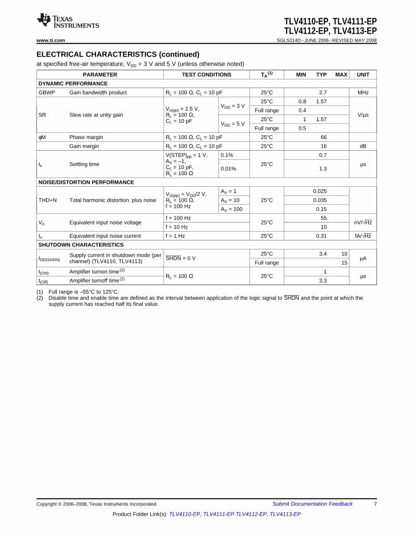
ELECTRICAL CHARACTERISTICS (continued)
TLV4110-EP, TLV4111-EPTLV4112-EP, TLV4113-EPSGLS314D–JUNE 2006–REVISED MAY 2008............................................................................................................................................................... www.ti.com
at specified free-air temperature, VDD = 3 V and 5 V (unless otherwise noted)
PARAMETER TEST CONDITIONS TA(1) MIN TYP MAX UNIT
OUTPUT CHARACTERISTICS25°C 2.7 2.97
IOH = –10 mAFull range 2.6VDD = 3 V, VVIC = VDD/2 25°C 2.6 2.73
IOH = –100 mAFull range 2.5
VOH High-level output voltage25°C 4.7 4.96
IOH = –10 mAFull range 4.6VDD = 5 V, VVIC = VDD/2 25°C 4.6 4.76
IOH = –100 mAFull range 4.5
25°C 0.03 0.1IOL = 10 mA
Full range 0.2VDD = 3 V and 5 V,VOL Low-level output voltage VVIC = VDD/2 25°C 0.33 0.4IOL = 100 mA
Full range 0.55VDD = 3 V ±220Measured at 0.5 VIO Output current 25°C mAfrom rail VDD = 5 V ±320
Sourcing 800IOS Short-circuit output current 25°C mA
Sinking 800POWER SUPPLY
25°C 700 1000IDD Supply current (per channel) VO = VDD/2 µA
Full range 150025°C 69 82VDD = 2.7 to 3.3 V, No load dBVIC = VDD/2 V Full range 65Power supply rejection ratioPSRR (ΔVDD / ΔVIO) 25°C 69 79VDD = 4.5 to 5.5 V, No load dBVIC = VDD/2 V Full range 65
(1) Full range is –55°C to 125°C.
6 Submit Documentation Feedback Copyright © 2006–2008, Texas Instruments Incorporated
Product Folder Link(s): TLV4110-EP, TLV4111-EP TLV4112-EP, TLV4113-EP
ELECTRICAL CHARACTERISTICS (continued)
TLV4110-EP, TLV4111-EPTLV4112-EP, TLV4113-EP
www.ti.com............................................................................................................................................................... SGLS314D–JUNE 2006–REVISED MAY 2008
at specified free-air temperature, VDD = 3 V and 5 V (unless otherwise noted)
PARAMETER TEST CONDITIONS TA(1) MIN TYP MAX UNIT
DYNAMIC PERFORMANCEGBWP Gain bandwidth product RL = 100 Ω, CL = 10 pF 25°C 2.7 MHz
25°C 0.8 1.57VDD = 3 VVo(pp) = 2.5 V, Full range 0.4
SR Slew rate at unity gain RL = 100 Ω, V/µs25°C 1 1.57CL = 10 pF VDD = 5 V
Full range 0.5φM Phase margin RL = 100 Ω, CL = 10 pF 25°C 66
Gain margin RL = 100 Ω, CL = 10 pF 25°C 16 dBV(STEP)pp = 1 V, 0.1% 0.7AV = –1,ts Settling time 25°C µsCL = 10 pF, 0.01% 1.3RL = 100 Ω
NOISE/DISTORTION PERFORMANCEAV = 1 0.025VO(pp) = VDD/2 V,
THD+N Total harmonic distortion, plus noise RL = 100 Ω, AV = 10 25°C 0.035f = 100 Hz AV = 100 0.15f = 100 Hz 55
Vn Equivalent input noise voltage 25°C nV/√Hzf = 10 Hz 10
In Equivalent input noise current f = 1 Hz 25°C 0.31 fA/√HzSHUTDOWN CHARACTERISTICS
25°C 3.4 10Supply current in shutdown mode (perIDD(SHDN) SHDN = 0 V µAchannel) (TLV4110, TLV4113) Full range 15t(ON) Amplifier turnon time (2) 1
RL = 100 Ω 25°C µst(Off) Amplifier turnoff time (2) 3.3
(1) Full range is –55°C to 125°C.(2) Disable time and enable time are defined as the interval between application of the logic signal to SHDN and the point at which the
supply current has reached half its final value.
Copyright © 2006–2008, Texas Instruments Incorporated Submit Documentation Feedback 7
Product Folder Link(s): TLV4110-EP, TLV4111-EP TLV4112-EP, TLV4113-EP

TYPICAL CHARACTERISTICS
40
50
60
70
80
90
100
110
120
f − Frequency − Hz
CM
RR
− C
omm
on-M
ode
Rej
ectio
n R
atio
− d
B
100 1k 10k 10M100k 1M
G003
VDD = 3 VTA = 25°C
VICR − Common-Mode Input V oltage − V
−6000
−4000
−2000
0
2000
4000
6000
−0.2 0.4 1.0 1.6 2.2 2.8 3.4 4.0 4.6 5.2
VIO
− In
put O
ffset
Vol
tage
− µ
V
G002
VDD = 5 VTA = 25°C
VICR − Common-Mode Input V oltage − V
−6000
−4000
−2000
0
2000
4000
6000
−0.4 0.0 0.4 0.8 1.2 1.6 2.0 2.4 2.8 3.2
VIO
− In
put O
ffset
Vol
tage
− µ
V
G001
VDD = 3 VTA = 25°C
TLV4110-EP, TLV4111-EPTLV4112-EP, TLV4113-EPSGLS314D–JUNE 2006–REVISED MAY 2008............................................................................................................................................................... www.ti.com
Table of GraphsFIGURE
VIO Input offset voltage vs Common-mode input voltage 2, 3CMRR Common-mode rejection ratio vs Frequency 4VOH High-level output voltage vs High-level output current 5, 7VOL Low-level output voltage vs Low-level output current 6, 8Zo Output impedance vs Frequency 9IDD Supply current vs Supply voltage 10kSVR Power supply voltage rejection ratio vs Frequency 11AVD Differential voltage amplification and phase vs Frequency 12
Gain-bandwidth product vs Supply voltage 13vs Supply voltage 14
SR Slew ratevs Temperature 15
Total harmonic distortion+noise vs Frequency 16Vn Equivalent input voltage noise vs Frequency 17
Phase margin vs Capacitive load 18Voltage-follower signal pulse response 19, 20Inverting large-signal pulse response 21Small-signal inverting pulse response 22Crosstalk vs Frequency 23Shutdown forward and reverse isolation 24Shutdown supply current vs Free-air temperature 25Shutdown supply current/output voltage 26
INPUT OFFSET VOLTAGE INPUT OFFSET VOLTAGE COMMON-MODE REJECTION RATIOvs vs vs
COMMON-MODE INPUT VOLTAGE COMMON-MODE INPUT VOLTAGE FREQUENCY
Figure 2. Figure 3. Figure 4.
8 Submit Documentation Feedback Copyright © 2006–2008, Texas Instruments Incorporated
Product Folder Link(s): TLV4110-EP, TLV4111-EP TLV4112-EP, TLV4113-EP

IOH − High-Level Output Current − mA
2.0
2.1
2.2
2.3
2.4
2.5
2.6
2.7
2.8
2.9
3.0
0 50 100 150 200 250 300
VO
H −
Hig
h-Le
vel O
utpu
t Vol
tage
− V
G004
VDD = 3 V
TA = 70C
TA = 25C
TA = 0C
TA = −40C
TA = 125C
IOL − Low-Level Output Current − mA
0.0
0.1
0.2
0.3
0.4
0.5
0.6
0.7
0.8
0.9
1.0
0 50 100 150 200 250 300
VO
L −
Low
-Lev
el O
utpu
t Vol
tage
− V
G005
VDD = 3 VTA = 70C
TA = 25C
TA = −40C
TA = 0C
TA = 125C
IOH − High-Level Output Current − mA
4.0
4.1
4.2
4.3
4.4
4.5
4.6
4.7
4.8
4.9
5.0
0 50 100 150 200 250 300
VO
H −
Hig
h-Le
vel O
utpu
t Vol
tage
− V
G006
VDD = 5 V
TA = 70C
TA = 25C
TA = 0C
TA = −40C
TA = 125C
f − Frequency − Hz
Zo
− O
utpu
t Im
peda
nce
− Ω
100 1k 10k 10M100k 1M
G008
0.1
1
100
10
VDD = 3 V and 5 VTA = 25°C
A = 100
A = 10
A = 1
VDD − Supply V oltage − V
0
200
400
600
800
1000
1200
0 1 2 3 4 5 6
I DD
− S
uppl
y C
urre
nt −
µA
G009
AV = 1VI = VDD/2 V
TA = 70C
TA = 25C
TA = 125C
TA = −40C
TA = 0C
IOL − Low-Level Output Current − mA
0.0
0.1
0.2
0.3
0.4
0.5
0.6
0.7
0.8
0.9
1.0
0 50 100 150 200 250 300
VO
L −
Low
-Lev
el O
utpu
t Vol
tage
− V
G007
VDD = 5 V
TA = 70C
TA = 25C
TA = 125C
TA = −40C
TA = 0C
−40
−20
0
20
40
60
80
100
120
f − Frequency − Hz
AV
D −
Diff
eren
tial V
olta
ge A
mpl
ifica
tion
− dB
100 1k 10k 10M100k 1M
G011
VDD = 3 V and 5 VRF = 100 kΩCL = 10 pFTA = 25°C
135
90
45
0
−45
Pha
se M
argi
n −
°
Phase
Gain
0
10
20
30
40
50
60
70
80
90
100
f − Frequency − Hz
PS
RR
− P
ower
Sup
ply
Rej
ectio
n R
atio
− V
100 1k 10k 10M100k 1M
G010
VDD = 3 V and 5 VRF = 1 kΩRI = 100 ΩVI = 0 VTA = 25°C
VDD − Supply V oltage − V
0.0
0.5
1.0
1.5
2.0
2.5
3.0
3.5
4.0
2.5 3.0 3.5 4.0 4.5 5.0 5.5
Gai
n-B
andw
idth
Pro
duct
− M
Hz
G012
RL = 100 ΩCL = 10 pFf = 1 kHzTA = 25°CAV = Open Loop
TLV4110-EP, TLV4111-EPTLV4112-EP, TLV4113-EP
www.ti.com............................................................................................................................................................... SGLS314D–JUNE 2006–REVISED MAY 2008
HIGH-LEVEL OUTPUT VOLTAGE LOW-LEVEL OUTPUT VOLTAGE HIGH-LEVEL OUTPUT VOLTAGEvs vs vs
HIGH-LEVEL OUTPUT CURRENT LOW-LEVEL OUTPUT CURRENT HIGH-LEVEL OUTPUT CURRENT
Figure 5. Figure 6. Figure 7.
LOW-LEVEL OUTPUT VOLTAGE OUTPUT IMPEDANCE SUPPLY CURRENTvs vs vs
LOW-LEVEL OUTPUT CURRENT FREQUENCY SUPPLY VOLTAGE
Figure 8. Figure 9. Figure 10.
POWER-SUPPLY REJECTION DIFFERENTIAL VOLTAGERATIO AMPLIFICATION AND PHASE GAIN-BANDWIDTH PRODUCT
vs vs vsFREQUENCY FREQUENCY SUPPLY VOLTAGE
Figure 11. Figure 12. Figure 13.
Copyright © 2006–2008, Texas Instruments Incorporated Submit Documentation Feedback 9
Product Folder Link(s): TLV4110-EP, TLV4111-EP TLV4112-EP, TLV4113-EP

f − Frequency − Hz
10
VDD = 5 VRL = 100 ΩVO(PP) = VDD/2AV = 1, 10, and 100
100 1k 100k
TH
D+N
− T
otal
Har
mon
ic D
isto
rtion
+ N
oise
− %
0.01
0.1
1
10
10k
A = 100
A = 10
A = 1
G015VDD − Supply V oltage − V
0.00
0.25
0.50
0.75
1.00
1.25
1.50
1.75
2.00
2.5 3.0 3.5 4.0 4.5 5.0 5.5 6.0
SR
− S
lew
Rat
e −
V/µ
s
G013
RL = 100 ΩCL = 10 pFAV = 1
SR+
SR−
TA − Free-Air T emperature − °C
0.00
0.25
0.50
0.75
1.00
1.25
1.50
1.75
2.00
−40 −25 −10 5 20 35 50 65 80 95 110 125
SR
− S
lew
Rat
e −
V/µ
s
G014
SR+
SR−
VDD = 3 V and 5 VRL = 100 ΩCL = 10 pFAV = 1
0
20
40
60
80
100
120
140
160
f − Frequency − Hz
Vn
− E
quiv
alen
t Inp
ut V
olta
ge N
oise
− n
V/H
z
10 100 1k 100k10k
VDD = 5 V
G016
VDD = 3 V
0
10
20
30
40
50
60
70
80
90
100
Capacitive Load − pF
VDD = 3 V and 5 VTA = 25°C
Pha
se M
argi
n −
°
10 100 1k 100k10k
RL = 100
G017
RL = 600 RNULL = 20
RNULL = 20
RNULL = 0
RNULL = 0
t − Time − µs
−2 0 2 4 6 8 10 12 14VO
− O
utpu
t Vol
tage
− V
G018
0
1
2
3
4
0
1
2
3
4
5
VI −
Inpu
t Vol
tage
− V
VI
VO
VDD = 5 VRL = 100 ΩCL = 10 pFTA = 25°CAV = 1
t − Time − µs
−0.2 0.0 0.2 0.4 0.6 0.8 1.0 1.2 1.4VO
− O
utpu
t Vol
tage
− V
G019
2.40
2.45
2.50
2.55
2.45
2.50
2.55
2.60
VI −
Inpu
t Vol
tage
− V VI
VO
VDD = 5 VRL = 100 ΩCL = 10 pFTA = 25°CVI = 100 mVAV = 1
t − Time − µs
−1 0 1 2 3 4 5 6 7 8VO
− O
utpu
t Vol
tage
− V
G020
0
1
2
3
4
−2
−1
0
1
2
3
VI −
Inpu
t Vol
tage
− V
VI
VO
VDD = 5 VRL = 100 ΩCL = 50 pFTA = 25°CVI = 2.5 VAV = −1
5
t − Time − µs
−0.2 0.2 0.6 1.0 1.4 1.8 2.2 2.6 3.0VO
− O
utpu
t Vol
tage
− V
G021
2.42
2.50
2.54
2.42
2.46
2.50
2.54
2.58
VI −
Inpu
t Vol
tage
− V
VI
VO
VDD = 5 VRL = 100 ΩCL = 50 pFTA = 25°CVI = 2.5 VAV = −1
2.46
TLV4110-EP, TLV4111-EPTLV4112-EP, TLV4113-EPSGLS314D–JUNE 2006–REVISED MAY 2008............................................................................................................................................................... www.ti.com
TOTAL HARMONICSLEW RATE SLEW RATE DISTORTION+NOISE
vs vs vsSUPPLY VOLTAGE TEMPERATURE FREQUENCY
Figure 14. Figure 15. Figure 16.
EQUIVALENT INPUT VOLTAGENOISE PHASE MARGIN
vs vs VOLTAGE-FOLLOWERFREQUENCY CAPACITIVE LOAD LARGE-SIGNAL PULSE RESPONSE
Figure 17. Figure 18. Figure 19.
VOLTAGE-FOLLOWER INVERTING LARGE-SIGNAL SMALL-SIGNAL INVERTINGSMALL-SIGNAL PULSE RESPONSE PULSE RESPONSE PULSE RESPONSE
Figure 20. Figure 21. Figure 22.
10 Submit Documentation Feedback Copyright © 2006–2008, Texas Instruments Incorporated
Product Folder Link(s): TLV4110-EP, TLV4111-EP TLV4112-EP, TLV4113-EP

−120
−100
−80
−60
−40
−20
0
f − Frequency − Hz
VDD = 3 V and 5 VRL = 100 ΩAll Channels
Cro
ssta
lk −
dB
10 100 1k 100k10k
G022
VI = 4 VPP
VI = 2 VPP
−160
−140
−120
−100
−80
−60
−40
−20
0
f − Frequency − Hz
VDD = 3 V and 5 VRL = 100 ΩCL = 50 pFTA = 25°CAV = 1
Shu
tdow
n F
/R Is
olat
ion
− dB
10 100 1k 10M10k
G023
VI = 0.1 VPP
VI = 2.5 VPP
100k 1M
TA − Free-Air T emperature − °C
−2
0
2
4
6
8
10
12
14
16
−40 −25 −10 5 20 35 50 65 80 95 110 125
I DD
− S
hutd
own
Sup
ply
Cur
rent
−
µA
G024
VDD = 3 V and 5 VVI = VDD/2No Load
t − Time − µsG025
−20 0 12020 40 60 80 100−2
4
3
2
1
0
2
1.5
0
2
4
6
0
0.5
1
VDD = 3 VRL = 100 ΩCL = 10 pFTA = 25°CVI = VDD/2AV = 1
IDD(SD)
VO
SD
I DD
(SD
) −
Shu
tdow
n S
uppl
y C
urre
nt −
µA
VO
− O
utpu
t Vol
tage
− V
SH
DN
− S
hutd
own
Pul
se −
V
TLV4110-EP, TLV4111-EPTLV4112-EP, TLV4113-EP
www.ti.com............................................................................................................................................................... SGLS314D–JUNE 2006–REVISED MAY 2008
CROSSTALK SHUTDOWN SUPPLY CURRENTvs SHUTDOWN FORWARD AND vs
FREQUENCY REVERSE ISOLATION FREE-AIR TEMPERATURE
Figure 23. Figure 24. Figure 25.SHUTDOWN SUPPLY CURRENT / OUTPUT VOLTAGE
Figure 26.
Copyright © 2006–2008, Texas Instruments Incorporated Submit Documentation Feedback 11
Product Folder Link(s): TLV4110-EP, TLV4111-EP TLV4112-EP, TLV4113-EP

APPLICATION INFORMATION
SHUTDOWN FUNCTION
DRIVING A CAPACITIVE LOAD
CLOAD
RF
InputOutput
RGRNULL
+
−
RL CL
RF
InputOutput
RGRNULL
+
−
RLSnubber
C
(a) (b)S0048-03
OFFSET VOLTAGE
VOO VIO1RFRG IIB RS1 RF
RG IIB RF
+
−VI
+
RG
RS
RF
IIB−
VO
IIB+
S0094-01
TLV4110-EP, TLV4111-EPTLV4112-EP, TLV4113-EPSGLS314D–JUNE 2006–REVISED MAY 2008............................................................................................................................................................... www.ti.com
Two members of the TLV411x family (TLV4110/3) have a shutdown terminal for conserving battery life inportable applications. When the shutdown terminal is tied low, the supply current is reduced to just nano ampsper channel, the amplifier is disabled, and the outputs are placed in a high-impedance mode. In order to savepower in shutdown mode, an external pullup resistor is required; therefore, to enable the amplifier, the shutdownterminal must be pulled high. When the shutdown terminal is left floating, care should be taken to ensure thatparasitic leakage current at the shutdown terminal does not inadvertently place the operational amplifier intoshutdown.
When the amplifier is configured in this manner, capacitive loading directly on the output decreases the device'sphase margin, leading to high-frequency ringing or oscillations. Therefore, for capacitive loads of greater than1 nF, it is recommended that a resistor be placed in series ®NULL) with the output of the amplifier, as shown inFigure 27. A maximum value of 20 Ω is recommended for most applications.
Figure 27. Driving a Capacitive Load
The output offset voltage, (VOO) is the sum of the input offset voltage (VIO) and both input bias currents (IIB) timesthe corresponding gains. The following schematic and formula can be used to calculate the output offset voltage.
Figure 28. Output Offset Voltage Model
12 Submit Documentation Feedback Copyright © 2006–2008, Texas Instruments Incorporated
Product Folder Link(s): TLV4110-EP, TLV4111-EP TLV4112-EP, TLV4113-EP

_
+
Rnull
RL CL
S0095-01
GENERAL POWER DESIGN CONSIDERATIONS
IDC(EQ) ICont (duty cycle)(1)
TLV4110-EP, TLV4111-EPTLV4112-EP, TLV4113-EP
www.ti.com............................................................................................................................................................... SGLS314D–JUNE 2006–REVISED MAY 2008
Figure 29.
When driving heavy loads at high junction temperatures there is an increased probability of electromigrationaffecting the long-term reliability of ICs. Therefore, to avoid this issue:• The output current must be limited (at these high-junction temperatures).
OR• The junction temperature must be limited.
The maximum continuous output current at a die temperature 150°C will be 1/3 of the current at 105°C.
The junction temperature will be dependent on the ambient temperature around the IC, thermal impedance fromthe die to the ambient and power dissipated within the IC.
TJ = TA + θJA × PDIS
Where:PDIS is the IC power dissipation and is equal to the output current multiplied by the voltage dropped acrossthe output of the IC.θJA is the thermal impedance between the junction and the ambient temperature of the IC.TJ is the junction temperature.TA is the ambient temperature.
Reducing one or more of these factors results in a reduced die temperature. The 8-pin SOIC (small outlineintegrated circuit) has a thermal impedance from junction to ambient of 176°C/W. For this reason it isrecommended that the maximum power dissipation of the 8-pin SOIC package be limited to 350 mW, with peakdissipation of 700 mW as long as the RMS value is less than 350 mW.
The use of the MSOP PowerPAD™ dramatically reduces the thermal impedance from junction to case. And, withcorrect mounting, the reduced thermal impedance greatly increases the IC's permissible power dissipation andoutput current handling capability. For example, the power dissipation of the PowerPAD™ is increased to above1 W. Sinusoidal and pulse-width modulated output signals also increase the output current capability. Theequivalent dc current is proportional to the square-root of the duty cycle:
CURRENT DUTY CYCLE EQUIVALENT DC CURRENTAT PEAK RATED CURRENT AS A PERCENTAGE OF PEAK
100 10070 8450 71
Copyright © 2006–2008, Texas Instruments Incorporated Submit Documentation Feedback 13
Product Folder Link(s): TLV4110-EP, TLV4111-EP TLV4112-EP, TLV4113-EP

GENERAL PowerPAD DESIGN CONSIDERATIONS
DIE
Side View (a)
End View (b) Bottom View (c)
DIE
ThermalPad
M0031-01
TLV4110-EP, TLV4111-EPTLV4112-EP, TLV4113-EPSGLS314D–JUNE 2006–REVISED MAY 2008............................................................................................................................................................... www.ti.com
Note that, with an operational amplifier, a duty cycle of 70% often results in the op-amp sourcing current 70% ofthe time and sinking current 30%; therefore, the equivalent dc current is still 0.84 times the continuous currentrating at a particular junction temperature.
The TLV411x is available in a thermally-enhanced PowerPAD family of packages. These packages areconstructed using a downset lead frame upon which the die is mounted [see Figure 30(a) and Figure 30(b)]. Thisarrangement results in the lead frame being exposed as a thermal pad on the underside of the package [seeFigure 30(c)]. Because this thermal pad has direct thermal contact with the die, excellent thermal performancecan be achieved by providing a good thermal path away from the thermal pad.
The PowerPAD package allows for both assembly and thermal management in one manufacturing operation.During the surface-mount solder operation (when the leads are being soldered), the thermal pad can also besoldered to a copper area underneath the package. Through the use of thermal paths within this copper area,heat can be conducted away from the package into either a ground plane or other heat-dissipating device.
The PowerPAD package represents a breakthrough in combining the small area and ease of assembly ofsurface mount with the previously awkward mechanical methods of heat sinking.
Figure 30. Views of Thermally Enhanced DGN Package
14 Submit Documentation Feedback Copyright © 2006–2008, Texas Instruments Incorporated
Product Folder Link(s): TLV4110-EP, TLV4111-EP TLV4112-EP, TLV4113-EP

68 mils × 70 mils) with 5 vias(Via diameter = 13 mils
Thermal Pad Area
Single or Dual
M0032−01
TLV4110-EP, TLV4111-EPTLV4112-EP, TLV4113-EP
www.ti.com............................................................................................................................................................... SGLS314D–JUNE 2006–REVISED MAY 2008
Although there are many ways to properly heatsink the PowerPAD package, the following steps illustrate therecommended approach.1. Prepare the PCB with a top-side etch pattern, as shown in Figure 31. There should be etch for the leads as
well as etch for the thermal pad.2. Place five holes (dual) or nine holes (quad) in the area of the thermal pad. These holes should be 13 mils in
diameter. Keep them small so that solder wicking through the holes is not a problem during reflow.3. Additional vias may be placed anywhere along the thermal plane outside of the thermal pad area. This helps
dissipate the heat generated by the TLV411x IC. These additional vias may be larger than the 13-mildiameter vias directly under the thermal pad. They can be larger because they are not in the thermal padarea to be soldered so that wicking is not a problem.
4. Connect all holes to the internal ground plane.5. When connecting these holes to the ground plane, do not use the typical web or spoke via connection
methodology. Web connections have a high thermal-resistance connection that is useful for slowing the heattransfer during soldering operations. This makes the soldering of vias that have plane connections easier. Inthis application, however, low thermal resistance is desired for the most efficient heat transfer. Therefore, theholes under the TLV411x PowerPAD package should make their connection to the internal ground plane witha complete connection around the entire circumference of the plated-through hole.
6. The top-side solder mask should leave the terminals of the package and the thermal pad area with its fiveholes (dual) or nine holes (quad) exposed. The bottom-side solder mask should cover the five or nine holesof the thermal pad area. This prevents solder from being pulled away from the thermal pad area during thereflow process.
7. Apply solder paste to the exposed thermal pad area and all of the IC terminals.8. With these preparatory steps in place, the TLV411x IC is simply placed in position and run through the solder
reflow operation as any standard surface-mount component. This results in a part that is properly installed.
Figure 31. PowerPAD PCB Etch and Via Pattern
Copyright © 2006–2008, Texas Instruments Incorporated Submit Documentation Feedback 15
Product Folder Link(s): TLV4110-EP, TLV4111-EP TLV4112-EP, TLV4113-EP

PD TMAX–TAJA
Where:
PD = Maximum power dissipation of TLV411x IC (watts)TMAX = Absolute maximum junction temperature (150°C)TA = Free-ambient air temperature (°C)θJA = θJC + θCA
θJC = Thermal coefficient from junction to caseθCA = Thermal coefficient from case to ambient air (°C/W) (2)
TA − Free-Air T emperature − °C
0.0
0.5
1.0
1.5
2.0
2.5
3.0
3.5
4.0
−55 −40 −25 −10 5 20 35 50 65 80 95 110 125
Max
imum
Pow
er D
issi
patio
n −
W
G026
TJ = 150°C
DGN PackageLow-K T est PCBθJA = 52.7°C/W
SOIC PackageLow-K T est PCBθJA = 176°C/W
TLV4110-EP, TLV4111-EPTLV4112-EP, TLV4113-EPSGLS314D–JUNE 2006–REVISED MAY 2008............................................................................................................................................................... www.ti.com
For a given θJA, the maximum power dissipation is shown in Figure 32 and is calculated by the following formula:
NOTE: Results are with no air flow and using JEDEC Standard Low-K test PCB.
Figure 32. Maximum Power Dissipation vs Free-Air Temperature
The next consideration is the package constraints. The two sources of heat within an amplifier are quiescentpower and output power. The designer should never forget about the quiescent heat generated within the device,especially multi-amplifier devices. Because these devices have linear output stages (Class A-B), most of the heatdissipation is at low output voltages with high output currents.
The other key factor when dealing with power dissipation is how the devices are mounted on the PCB. ThePowerPAD devices are extremely useful for heat dissipation. But, the device should always be soldered to acopper plane to fully use the heat dissipation properties of the PowerPAD. The SOIC package, on the otherhand, is highly dependent on how it is mounted on the PCB. As more trace and copper area is placed around thedevice, θJA decreases and the heat-dissipation capability increases. The currents and voltages shown in thesegraphs are for the total package. For the dual or quad amplifier packages, the sum of the RMS output currentsand voltages should be used to choose the proper package.
16 Submit Documentation Feedback Copyright © 2006–2008, Texas Instruments Incorporated
Product Folder Link(s): TLV4110-EP, TLV4111-EP TLV4112-EP, TLV4113-EP

MACROMODEL INFORMATION
* TLV4112_5V operational amplifier ”macromodel” subcircuit* updated using Model Editor release 9.1 on 01/18/00 at 15:50Model Editor is an OrCAD product.** connections: non−inverting input* | inverting input* | | positive power supply* | | | negative power supply* | | | | output* | | | | |.subckt TLV4112_5V 1 2 3 4 5*
c1 11 12 2.2439E−12c2 6 7 10.000E−12css 10 99 454.55E−15dc 5 53 dyde 54 5 dydlp 90 91 dxdln 92 90 dxdp 4 3 dx
egnd 99 0 poly(2) (3,0) (4,0) 0 .5 .5 fb 7 99 poly(5) vb vc ve vlp vln 0
+ 33.395E6 −1E3 1E3 33E6 −33E6 ga 6 0 11 12 168.39E−6 gcm 0 6 10 99 168.39E−12
iss 10 4 dc 13.800E−6hlim 90 0 vlim 1Kioff 0 6 dc 75E−9j1 11 2 10 jx1J2 12 1 10 jx2r2 6 9 100.00E3rd1 3 11 5.9386E3rd2 3 12 5.9386E3ro1 8 5 10ro2 7 99 10rp 3 4 3.3333E3rss 10 99 14.493E6vb 9 0 dc 0vc 3 53 dc .86795ve 54 4 dc .86795vlim 7 8 dc 0vlp 91 0 dc 300vln 0 92 dc 300.model dx D(Is=800.00E−18).model dy D(Is=800.00E−18 Rs=1m Cjo=10p).model jx1 NJF(Is=150.00E−12 Beta=2.0547E−3 +Vto=−1).model jx2 NJF(Is=150.00E−12 Beta=2.0547E−3 + Vto=−1).ends*$
IN−G
D
S
D
S
G
rp
IN+
rd1 rd2 rss egnd fb ro2
ro1
vlim
OUT
ga
ioffgcm
vb
c1
dciss
dp
GND
VDD
css
c2
ve de
dlp dln
vlnhlimvlp
10
4
1
11 12
3
53
54
9 6
8
5
7
91 90 92
vc
99
+
+
+
+
+
++
−
−
−
−
−−
−
− +
r2
2
S0096-01
TLV4110-EP, TLV4111-EPTLV4112-EP, TLV4113-EP
www.ti.com............................................................................................................................................................... SGLS314D–JUNE 2006–REVISED MAY 2008
Macromodel information provided was derived using Microsim Parts™, the model generation software used withMicrosim PSpice™ The Boyle macromodel (see Note 3) and subcircuit in Figure 33 are generated using theTLV411x typical electrical and operating characteristics at TA = 25°C. Using this information, output simulationsof the following key parameters can be generated to a tolerance of 20% (in most cases).
• Common-mode rejection ratio• Maximum positive output voltage swing• Phase margin• Maximum negative output voltage swing• DC output resistance• Slew rate• AC output resistance• Quiescent power dissipation• Short-circuit output current limit• Input bias current
• Open-loop voltage amplification• Unity-gain frequencyNOTE 3: G.R. Boyle, B. M. Cohn, D. O. Pederson, and J. E. Solomon, "Macromodeling of Integrated Circuit Operational Amplifiers," IEEE Journal of Solid-StateCircuits, SC-9, 353 (1974).
Figure 33. Boyle Macromodel and Subcircuit
Copyright © 2006–2008, Texas Instruments Incorporated Submit Documentation Feedback 17
Product Folder Link(s): TLV4110-EP, TLV4111-EP TLV4112-EP, TLV4113-EP
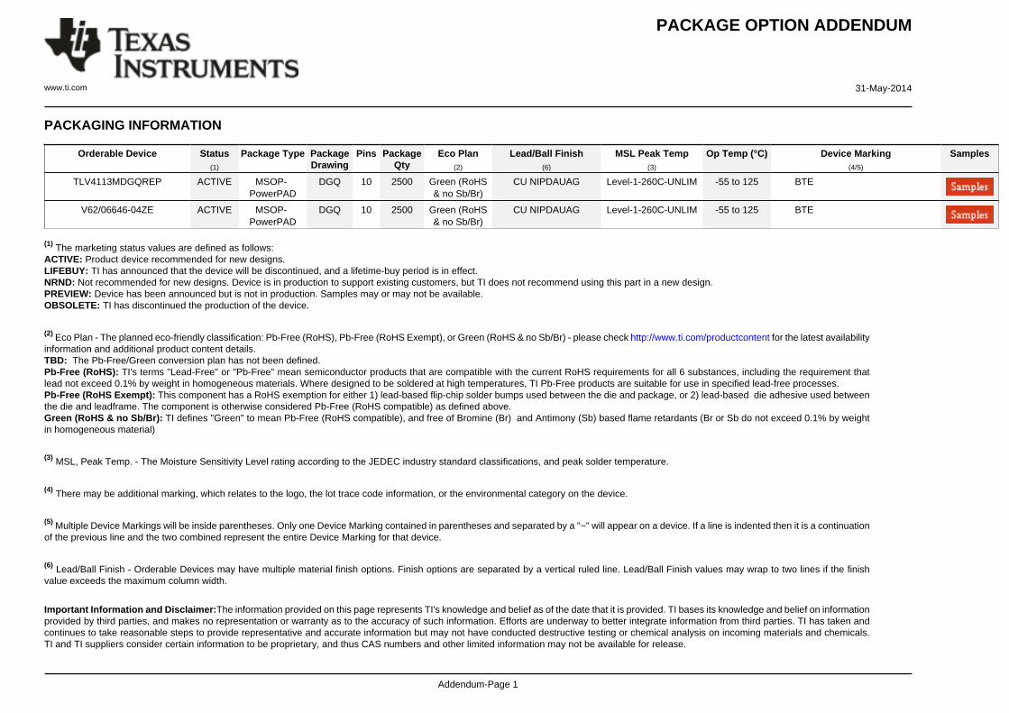
PACKAGE OPTION ADDENDUM
www.ti.com 31-May-2014
Addendum-Page 1
PACKAGING INFORMATION
Orderable Device Status(1)
Package Type PackageDrawing
Pins PackageQty
Eco Plan(2)
Lead/Ball Finish(6)
MSL Peak Temp(3)
Op Temp (°C) Device Marking(4/5)
Samples
TLV4113MDGQREP ACTIVE MSOP-PowerPAD
DGQ 10 2500 Green (RoHS& no Sb/Br)
CU NIPDAUAG Level-1-260C-UNLIM -55 to 125 BTE
V62/06646-04ZE ACTIVE MSOP-PowerPAD
DGQ 10 2500 Green (RoHS& no Sb/Br)
CU NIPDAUAG Level-1-260C-UNLIM -55 to 125 BTE
(1) The marketing status values are defined as follows:ACTIVE: Product device recommended for new designs.LIFEBUY: TI has announced that the device will be discontinued, and a lifetime-buy period is in effect.NRND: Not recommended for new designs. Device is in production to support existing customers, but TI does not recommend using this part in a new design.PREVIEW: Device has been announced but is not in production. Samples may or may not be available.OBSOLETE: TI has discontinued the production of the device.
(2) Eco Plan - The planned eco-friendly classification: Pb-Free (RoHS), Pb-Free (RoHS Exempt), or Green (RoHS & no Sb/Br) - please check http://www.ti.com/productcontent for the latest availabilityinformation and additional product content details.TBD: The Pb-Free/Green conversion plan has not been defined.Pb-Free (RoHS): TI's terms "Lead-Free" or "Pb-Free" mean semiconductor products that are compatible with the current RoHS requirements for all 6 substances, including the requirement thatlead not exceed 0.1% by weight in homogeneous materials. Where designed to be soldered at high temperatures, TI Pb-Free products are suitable for use in specified lead-free processes.Pb-Free (RoHS Exempt): This component has a RoHS exemption for either 1) lead-based flip-chip solder bumps used between the die and package, or 2) lead-based die adhesive used betweenthe die and leadframe. The component is otherwise considered Pb-Free (RoHS compatible) as defined above.Green (RoHS & no Sb/Br): TI defines "Green" to mean Pb-Free (RoHS compatible), and free of Bromine (Br) and Antimony (Sb) based flame retardants (Br or Sb do not exceed 0.1% by weightin homogeneous material)
(3) MSL, Peak Temp. - The Moisture Sensitivity Level rating according to the JEDEC industry standard classifications, and peak solder temperature.
(4) There may be additional marking, which relates to the logo, the lot trace code information, or the environmental category on the device.
(5) Multiple Device Markings will be inside parentheses. Only one Device Marking contained in parentheses and separated by a "~" will appear on a device. If a line is indented then it is a continuationof the previous line and the two combined represent the entire Device Marking for that device.
(6) Lead/Ball Finish - Orderable Devices may have multiple material finish options. Finish options are separated by a vertical ruled line. Lead/Ball Finish values may wrap to two lines if the finishvalue exceeds the maximum column width.
Important Information and Disclaimer:The information provided on this page represents TI's knowledge and belief as of the date that it is provided. TI bases its knowledge and belief on informationprovided by third parties, and makes no representation or warranty as to the accuracy of such information. Efforts are underway to better integrate information from third parties. TI has taken andcontinues to take reasonable steps to provide representative and accurate information but may not have conducted destructive testing or chemical analysis on incoming materials and chemicals.TI and TI suppliers consider certain information to be proprietary, and thus CAS numbers and other limited information may not be available for release.

PACKAGE OPTION ADDENDUM
www.ti.com 31-May-2014
Addendum-Page 2
In no event shall TI's liability arising out of such information exceed the total purchase price of the TI part(s) at issue in this document sold by TI to Customer on an annual basis.
OTHER QUALIFIED VERSIONS OF TLV4113-EP :
• Catalog: TLV4113
NOTE: Qualified Version Definitions:
• Catalog - TI's standard catalog product

TAPE AND REEL INFORMATION
*All dimensions are nominal
Device PackageType
PackageDrawing
Pins SPQ ReelDiameter
(mm)
ReelWidth
W1 (mm)
A0(mm)
B0(mm)
K0(mm)
P1(mm)
W(mm)
Pin1Quadrant
TLV4113MDGQREP MSOP-Power PAD
DGQ 10 2500 330.0 12.4 5.3 3.4 1.4 8.0 12.0 Q1
PACKAGE MATERIALS INFORMATION
www.ti.com 2-Mar-2012
Pack Materials-Page 1

*All dimensions are nominal
Device Package Type Package Drawing Pins SPQ Length (mm) Width (mm) Height (mm)
TLV4113MDGQREP MSOP-PowerPAD DGQ 10 2500 358.0 335.0 35.0
PACKAGE MATERIALS INFORMATION
www.ti.com 2-Mar-2012
Pack Materials-Page 2
IMPORTANT NOTICE
Texas Instruments Incorporated and its subsidiaries (TI) reserve the right to make corrections, enhancements, improvements and otherchanges to its semiconductor products and services per JESD46, latest issue, and to discontinue any product or service per JESD48, latestissue. Buyers should obtain the latest relevant information before placing orders and should verify that such information is current andcomplete. All semiconductor products (also referred to herein as “components”) are sold subject to TI’s terms and conditions of salesupplied at the time of order acknowledgment.TI warrants performance of its components to the specifications applicable at the time of sale, in accordance with the warranty in TI’s termsand conditions of sale of semiconductor products. Testing and other quality control techniques are used to the extent TI deems necessaryto support this warranty. Except where mandated by applicable law, testing of all parameters of each component is not necessarilyperformed.TI assumes no liability for applications assistance or the design of Buyers’ products. Buyers are responsible for their products andapplications using TI components. To minimize the risks associated with Buyers’ products and applications, Buyers should provideadequate design and operating safeguards.TI does not warrant or represent that any license, either express or implied, is granted under any patent right, copyright, mask work right, orother intellectual property right relating to any combination, machine, or process in which TI components or services are used. Informationpublished by TI regarding third-party products or services does not constitute a license to use such products or services or a warranty orendorsement thereof. Use of such information may require a license from a third party under the patents or other intellectual property of thethird party, or a license from TI under the patents or other intellectual property of TI.Reproduction of significant portions of TI information in TI data books or data sheets is permissible only if reproduction is without alterationand is accompanied by all associated warranties, conditions, limitations, and notices. TI is not responsible or liable for such altereddocumentation. Information of third parties may be subject to additional restrictions.Resale of TI components or services with statements different from or beyond the parameters stated by TI for that component or servicevoids all express and any implied warranties for the associated TI component or service and is an unfair and deceptive business practice.TI is not responsible or liable for any such statements.Buyer acknowledges and agrees that it is solely responsible for compliance with all legal, regulatory and safety-related requirementsconcerning its products, and any use of TI components in its applications, notwithstanding any applications-related information or supportthat may be provided by TI. Buyer represents and agrees that it has all the necessary expertise to create and implement safeguards whichanticipate dangerous consequences of failures, monitor failures and their consequences, lessen the likelihood of failures that might causeharm and take appropriate remedial actions. Buyer will fully indemnify TI and its representatives against any damages arising out of the useof any TI components in safety-critical applications.In some cases, TI components may be promoted specifically to facilitate safety-related applications. With such components, TI’s goal is tohelp enable customers to design and create their own end-product solutions that meet applicable functional safety standards andrequirements. Nonetheless, such components are subject to these terms.No TI components are authorized for use in FDA Class III (or similar life-critical medical equipment) unless authorized officers of the partieshave executed a special agreement specifically governing such use.Only those TI components which TI has specifically designated as military grade or “enhanced plastic” are designed and intended for use inmilitary/aerospace applications or environments. Buyer acknowledges and agrees that any military or aerospace use of TI componentswhich have not been so designated is solely at the Buyer's risk, and that Buyer is solely responsible for compliance with all legal andregulatory requirements in connection with such use.TI has specifically designated certain components as meeting ISO/TS16949 requirements, mainly for automotive use. In any case of use ofnon-designated products, TI will not be responsible for any failure to meet ISO/TS16949.
Products ApplicationsAudio www.ti.com/audio Automotive and Transportation www.ti.com/automotiveAmplifiers amplifier.ti.com Communications and Telecom www.ti.com/communicationsData Converters dataconverter.ti.com Computers and Peripherals www.ti.com/computersDLP® Products www.dlp.com Consumer Electronics www.ti.com/consumer-appsDSP dsp.ti.com Energy and Lighting www.ti.com/energyClocks and Timers www.ti.com/clocks Industrial www.ti.com/industrialInterface interface.ti.com Medical www.ti.com/medicalLogic logic.ti.com Security www.ti.com/securityPower Mgmt power.ti.com Space, Avionics and Defense www.ti.com/space-avionics-defenseMicrocontrollers microcontroller.ti.com Video and Imaging www.ti.com/videoRFID www.ti-rfid.comOMAP Applications Processors www.ti.com/omap TI E2E Community e2e.ti.comWireless Connectivity www.ti.com/wirelessconnectivity
Mailing Address: Texas Instruments, Post Office Box 655303, Dallas, Texas 75265Copyright © 2015, Texas Instruments Incorporated