High Mobility, Printable, and Solution-Processed Graphene ... files/E-publications... · High...
7
High Mobility, Printable, and Solution-Processed Graphene Electronics Shuai Wang, †,| Priscilla Kailian Ang, †,‡,| Ziqian Wang, § Ai Ling Lena Tang, † John T. L. Thong, § and Kian Ping Loh* ,† † Department of Chemistry, National University of Singapore, 3 Science Drive 3, Singapore 117543, ‡ NUS Graduate School for Integrative Sciences and Engineering, Singapore 117597, and § Department of Electrical and Computer Engineering, 4 Engineering Drive 3, Singapore 117576 ABSTRACT The ability to print graphene sheets onto large scale, flexible substrates holds promise for large scale, transparent electronics on flexible substrates. Solution processable graphene sheets derived from graphite can form stable dispersions in solutions and are amenable to bulk scale processing and ink jet printing. However, the electrical conductivity and carrier mobilities of this material are usually reported to be orders of magnitude poorer than that of the mechanically cleaved counterpart due to its higher density of defects, which restricts its use in electronics. Here, we show that by optimizing several key factors in processing, we are able to fabricate high mobility graphene films derived from large sized graphene oxide sheets, which paves the way for all-carbon post-CMOS electronics. All-carbon source-drain channel electronics fabricated from such films exhibit significantly improved transport characteristics, with carrier mobilities of 365 cm 2 /(V·s) for hole and 281 cm 2 /(V·s) for electron, measured in air at room temperature. In particular, intrinsic mobility as high as 5000 cm 2 /(V·s) can be obtained from such solution-processed graphene films when ionic screening is applied to nullify the Coulombic scattering by charged impurities. KEYWORDS Graphene, high mobility transistor, solution-processed, printable electronics, ionic screening, doping, impurity scattering T he discovery of graphene has revolutionized the field of electronics owing to its excellent electronic proper- ties and chemical and mechanical stability, which paves the way for ultrafast electronic devices and bio- and chemical sensors. 1,2 The mechanical exfoliation, or “Scotch tape” method, has been used to produce the first high-quality graphene sheets which set the performance standard for graphene produced by other methods. However, the “Scotch tape” method is not compatible with large-scale industrial processing and precludes the widespread implementation of graphene electronics; thus there are intense efforts world- wide to discover upwardly scalable production methods for high-quality graphene. Recent breakthroughs include the large-area deposition of few-layer graphene (FLG) using chemical vapor deposition on catalyst-coated substrates. 3 Another research thrust involves the solution processing of graphene derivatives. Chemical exfoliation methods which produce graphene oxide from graphite result in high-yield production of single sheet dispersions. 4,5 The solution- processability of GO offers unique advantages since it is readily amenable to spin-coating, spray-casting, drop-cast- ing, or inkjet printing onto substrates for large-scale produc- tion of graphene electronic circuits. The deoxidation of graphene oxide (GO) by chemical reduction and thermal annealing has been shown to produce zero-band-gap semi- metal graphene nanosheets which can exhibit trap-free band transport despite defects and disorder. 6 However, the tran- sistor carrier mobility in such a GO-derived graphene thin film is usually between 0.1 and 1 cm 2 /(V·s) as reported in literature, 4,6,7 which is several orders lower than that of the mechanically cleaved graphene. There are several possibili- ties for the poor performance in these chemically processed graphene (CPG). The charge percolation is limited by discon- nected network of π-delocalized tracks in these CPG. Defects created after the removal of C-O functional groups hinder the full recovery of the charge transport properties of pristine graphene 8 and further processing is needed to recover the extended aromatic framework. Therefore, there are still significant challenges ahead before CPG can be used in high mobility electronic devices. In this work, we discovered that by optimizing several key factors in film processing and device fabrication, unprec- edented performance in the electrical transport properties of CPG can be obtained. Our results reaffirm that CPG retains the intrinsic structural coherence for high mobility transport. Building upon this, we have also explored the premise of using CPG for inkjet printable all-carbon electronics. For electronic applications, the mobility and conductivity of graphene sheets are critical. 8 However it is widely known that the electrical characteristics of CPG are generally very poor. A survey of most reports found that a large percentage of CPG consists of GO flakes with sizes 1 µm or less due to prolonged ultrasonication and harsh oxidation treatment of the colloidal GO suspension. 4-11 We have a simple hypoth- * Corresponding author, [email protected]. | These authors contributed equally. Received for review: 09/2/2009 Published on Web: 12/21/2009 pubs.acs.org/NanoLett © 2010 American Chemical Society 92 DOI: 10.1021/nl9028736 | Nano Lett. 2010, 10, 92-98
Transcript of High Mobility, Printable, and Solution-Processed Graphene ... files/E-publications... · High...

High Mobility, Printable, andSolution-Processed Graphene ElectronicsShuai Wang,†,| Priscilla Kailian Ang,†,‡,| Ziqian Wang,§ Ai Ling Lena Tang,†John T. L. Thong,§ and Kian Ping Loh*,†
†Department of Chemistry, National University of Singapore, 3 Science Drive 3, Singapore 117543, ‡NUS GraduateSchool for Integrative Sciences and Engineering, Singapore 117597, and §Department of Electrical and ComputerEngineering, 4 Engineering Drive 3, Singapore 117576
ABSTRACT The ability to print graphene sheets onto large scale, flexible substrates holds promise for large scale, transparentelectronics on flexible substrates. Solution processable graphene sheets derived from graphite can form stable dispersions in solutionsand are amenable to bulk scale processing and ink jet printing. However, the electrical conductivity and carrier mobilities of thismaterial are usually reported to be orders of magnitude poorer than that of the mechanically cleaved counterpart due to its higherdensity of defects, which restricts its use in electronics. Here, we show that by optimizing several key factors in processing, we areable to fabricate high mobility graphene films derived from large sized graphene oxide sheets, which paves the way for all-carbonpost-CMOS electronics. All-carbon source-drain channel electronics fabricated from such films exhibit significantly improved transportcharacteristics, with carrier mobilities of 365 cm2/(V·s) for hole and 281 cm2/(V·s) for electron, measured in air at room temperature.In particular, intrinsic mobility as high as 5000 cm2/(V·s) can be obtained from such solution-processed graphene films when ionicscreening is applied to nullify the Coulombic scattering by charged impurities.
KEYWORDS Graphene, high mobility transistor, solution-processed, printable electronics, ionic screening, doping, impurityscattering
The discovery of graphene has revolutionized the fieldof electronics owing to its excellent electronic proper-ties and chemical and mechanical stability, which
paves the way for ultrafast electronic devices and bio- andchemical sensors.1,2 The mechanical exfoliation, or “Scotchtape” method, has been used to produce the first high-qualitygraphene sheets which set the performance standard forgraphene produced by other methods. However, the “Scotchtape” method is not compatible with large-scale industrialprocessing and precludes the widespread implementationof graphene electronics; thus there are intense efforts world-wide to discover upwardly scalable production methods forhigh-quality graphene. Recent breakthroughs include thelarge-area deposition of few-layer graphene (FLG) usingchemical vapor deposition on catalyst-coated substrates.3
Another research thrust involves the solution processing ofgraphene derivatives. Chemical exfoliation methods whichproduce graphene oxide from graphite result in high-yieldproduction of single sheet dispersions.4,5 The solution-processability of GO offers unique advantages since it isreadily amenable to spin-coating, spray-casting, drop-cast-ing, or inkjet printing onto substrates for large-scale produc-tion of graphene electronic circuits. The deoxidation ofgraphene oxide (GO) by chemical reduction and thermalannealing has been shown to produce zero-band-gap semi-
metal graphene nanosheets which can exhibit trap-free bandtransport despite defects and disorder.6 However, the tran-sistor carrier mobility in such a GO-derived graphene thinfilm is usually between 0.1 and 1 cm2/(V·s) as reported inliterature,4,6,7 which is several orders lower than that of themechanically cleaved graphene. There are several possibili-ties for the poor performance in these chemically processedgraphene (CPG). The charge percolation is limited by discon-nected network of π-delocalized tracks in these CPG. Defectscreated after the removal of C-O functional groups hinderthe full recovery of the charge transport properties of pristinegraphene8 and further processing is needed to recover theextended aromatic framework. Therefore, there are stillsignificant challenges ahead before CPG can be used in highmobility electronic devices.
In this work, we discovered that by optimizing several keyfactors in film processing and device fabrication, unprec-edented performance in the electrical transport propertiesof CPG can be obtained. Our results reaffirm that CPG retainsthe intrinsic structural coherence for high mobility transport.Building upon this, we have also explored the premise ofusing CPG for inkjet printable all-carbon electronics.
For electronic applications, the mobility and conductivityof graphene sheets are critical.8 However it is widely knownthat the electrical characteristics of CPG are generally verypoor. A survey of most reports found that a large percentageof CPG consists of GO flakes with sizes 1 µm or less due toprolonged ultrasonication and harsh oxidation treatment ofthe colloidal GO suspension.4-11 We have a simple hypoth-
* Corresponding author, [email protected].|These authors contributed equally.Received for review: 09/2/2009Published on Web: 12/21/2009
pubs.acs.org/NanoLett
© 2010 American Chemical Society 92 DOI: 10.1021/nl9028736 | Nano Lett. 2010, 10, 92-98

esis. We propose that the poor electrical characteristics canbe circumvented by using big sized GO (BSGOs) with lateralsize above 25 µm. Submicrometer sized GOs synthesizedby harsh oxidation conditions have a higher density ofdefects relative to BSGOs, due to the fact that the generationof smaller sized sheets from larger sized ones involveschemical destruction of aromatic bonds. The density of thesedefects may scale in a nonlinear way with the area of GOs;smaller GOs have a significantly larger density of disorderand defects on the basal planes due to a higher compositionof nonstoichiometric oxygen. Another important implicationin transport measurement is that for an edge-to-edge con-tinuous film constructed from networks of graphene flakes,the larger flakes should give a lower number of sheet-to-sheet junctions compared to the smaller flakes within a fixedchannel length.
Here we report a reproducible and simple method toobtain high-quality BSGO (Figure 1a) where more than 20%of the flakes have lateral dimension larger than 25 µm,according to size-counting using optical micrograph andscanning electron microscopy (SEM) images. Our methodis based on the modified Hummer’s method.7 We appliedcareful gradient separation and minimized the number ofsonication steps to avoid breaking up the larger sized GOsheets. (See Methods in Supporting Information.) Such BSGOsheets possess a significantly reduced number of C-Ogroups compared to small-sized GO, as evident from therelative proportion of the C-C bond versus C-O bonds inthe deconvoluted X-ray photoelectron spectroscopy (XPS)spectra. The deconvoluted area assignable to the C-C bondsof graphene (Figure 1d) is higher than that of small-sized GOby 10%.11 Despite a lower proportion of C-O groups, theaqueous solution of BSGO remains stable and opaque over
several months in concentrations as high as 50 mg mL-1
(Figure 1b). In addition, spin-coating of the BSGO solutiononto a SiO2/Si substrate allows the formation of a uniform,continuous graphene thin film as shown in Figure 1c wherethe film morphology probed by atomic force microscopy(AFM) shows incommensurately stacked BSGO sheets withthe edges of individual GO sheets clearly visible. By varyingthe concentration of BSGO solution, we are able to tune thethickness of the graphene film selectively from one to threelayers. Upon thermal annealing of BSGO-coated SiO2/Sisubstrate at 1000 °C, the C 1s peak signal assignable to theC-C bonds of graphene increases from 53% to 89%. AFMmeasurement also indicates a reduction of sheet thicknessfrom ∼1 nm, due to protruding oxygen groups on either sideof GO sheets, to 0.53 nm, a characteristic thickness ofgraphene sheet (see Figure S3 in Supporting Information).Significant structural changes reflective of the restoration ofdelocalized π-conjugation in GO-derived graphene sheets arealso evident from their Raman spectra (Figure 1d). The Gband for reduced BSGO is sharper and shifts to lowerfrequency (1586 cm-1) as compared to BSGO (1594 cm-1).The ratio of Raman D to G band intensity (ID/IG) decreasesfrom 0.81 to 0.78, thus indicating an increase in the averagesize of sp2 domains on reduced BSGO. The restoration of theπ-conjugated structure in the BSGO sheets translates to ahigh conductivity of 760 S/cm, which is close to that ofpolycrystalline graphite (1250 S/cm) (see Figures S4 and S5in Supporting Information). This makes these graphenesheets an attractive candidate for making continuous, highlyconducting graphene thin films by spin-coating or printingtechnologies amenable to large scale processing.
To investigate the transport characteristics of thesegraphene films, we fabricated graphene thin film field-effect
FIGURE 1. Big-sized GO (BSGO) sheets and their characterization. (a) AFM image of BSGO. (b) The narrow size distribution of BSGOs withGaussian mean at 250 ( 10 µm2. (c) AFM image of BSGO films showing good film morphology. Inset: GO solution remains stable after 5months with a concentration as high as 50 mg mL-1. (d) Deconvolution of XPS spectra and Raman spectra for BSGO before and after thermalannealing at 1000 °C.
© 2010 American Chemical Society 93 DOI: 10.1021/nl9028736 | Nano Lett. 2010, 10, 92-98

transistors (FET) with BSGO of varying thickness rangingfrom one to three layers (Figure 2). The thickness anduniformity of the graphene film were verified statistically byoptical contrast spectroscopy and AFM. Clear contrast dif-ference for single-layer, bilayer, and trilayer graphene filmsdeposited on a SiO2/Si surface with SiO2 thickness of 285nm can be observed from the contrast spectra generated bymeasuring the reflection spectra of white source light. Inaddition, tapping mode AFM topographical section analysiswas done randomly on 10 different areas of the SiO2/Sisubstrates (1 cm by 1 cm) which are coated with single-layer,bilayer, and trilayer graphene film to evaluate the thickness
and surface area coverage of graphene film. Graphene filmthickness (x) for single-layer graphene device is 0.5 < x e0.8 nm with a surface area coverage of 78 ( 8%, bilayergraphene device is 0.8 < x e 1.6 nm with surface areacoverage of 80 ( 7%, and trilayer graphene device is 1.6 <x e 2.4 nm with surface area coverage of 60 ( 5% (seeFigure S8 in Supporting Information). Oxygen plasma wasused to etch the graphene layers outside the active channelto reduce leakage current, which did not exceed 100 pA. Thecharge transport behavior of all graphene thin film FETs isrepresentative of the typical transport characteristic ofindividual mechanically cleaved graphene sheet as evi-
FIGURE 2. Single sheet graphene and thin graphene-based film field-effect transistor (FET). (a) Optical image of about single-layer reducedBSGO thin film with overlapping edges. (b) The transfer characteristics of single-layer reduced BSGO thin film FET with channel width W ∼31.8 µm, channel length L ∼ 26.92 µm, and hole and electron mobility of 5.4 and 1.1 cm2/(V·s), respectively, at constant Vds of 1 V. Insetshows the two-point probe measurement of the single-layer reduced BSGO thin film FET. Scale bar corresponds to 20 µm. (c) Optical imageof bilayer reduced BSGO thin film. (d) The transfer characteristics of bilayer reduced BSGO thin film FET with channel width W ∼ 32.55 µm,channel length L ∼ 30.00 µm, and hole and electron mobility of 50 and 10 cm2/(V·s), respectively, at constant Vds of 10 mV. Inset shows theschematic representation of the reduced BSGO thin film FET. (e) Optical image of about trilayer reduced BSGO thin film. (f) The transfercharacteristics of trilayer reduced BSGO thin film FET with channel width W ∼ 29.87 µm, channel length L ∼ 32.11 µm FET, and hole andelectron mobility of 92 and 51 cm2/(V·s), respectively at constant Vds of 10 mV. Inset shows the schematic representation of the reduced GOthin film FET. The thickness of gate dielectric SiO2 for all FETs is 285 nm.
© 2010 American Chemical Society 94 DOI: 10.1021/nl9028736 | Nano Lett. 2010, 10, 92-98

denced from the ambipolar behavior (panels b, d, and f ofFigure 2).2 The conductivity obtained for single-layer, bilayer,and trilayer graphene film is 58, 124, and 150 S/cm,respectively. Electron and hole mobility can be extractedfrom the linear regime of the transfer characteristics, usingµ ) [(∆Ids/Vds)(L/W)]/Cox ∆Vg where L and W are channellength and width respectively, Cox is silicon oxide gatecapacitance (which is 1.21 × 10⁻⁸ F/cm2 for a gate oxidethickness of 285 nm), Ids, Vds, and Vg are drain-sourcecurrent, drain-source voltage and gate voltage, respectively.From the I-Vg curves, we derive a maximum hole andelectron mobility of 5.4 and 1.1 cm2/(V·s) for the single-layergraphene film device, 50 and 10 cm2/(V·s) for the bilayergraphene film device, and 92 and 51 cm2/(V·s) for thetrilayer graphene film device, respectively. These values aresignificantly larger than the reported field effect transistormobilities of thin films derived from CPGs,4,6,7 thus substan-tiating that the high temperature annealing and large-sizedGOs in our case allow 2D charge percolation of the extendedπ-electron network. The π-electron systems in the CMGs aredisconnected due to regioselectivity in the deoxidationprocess, and a high temperature thermal annealing at 1000°C is needed to allow the coalescence of the initially isolatedπ-electron network.6 However, although these values aresignificantly larger than those reported for CPG thin films,
they are still at least 3 orders of magnitude lower than thosederived from mechanically cleaved graphene. Hence, thelimiting factors affecting charge carrier mobility were inves-tigated in the following sections.
The advantage of the solution-processable GOs is thatthey can be used to create large-scale all-carbon electrodesvia inkjet printing. This offers unique advantages overchemical vapor deposition method since no pre-patterningof catalysts is needed. Such graphene electrodes allow all-carbon contacts to be fabricated on graphene. Figure 3illustrates a schematic representation of two types of fabri-cation processes for printable graphene electrodes. In Figure3a-d, thick graphene electrodes are first drop-cast (orprinted) onto SiO2/Si substrates followed by spin-coating,drop-casting, or printing a thin layer of graphene over theseelectrodes to form all-carbon junctions. Figure 3e-h il-lustrates the combination of photolithography and conven-tional processes typically employed in the semiconductorindustry. First, narrow channels with width of 2 µm aredefined by photolithography. Next, graphene solution isdrop-cast (or printed) onto these channels which are subse-quently annealed at 150 °C for 20 min to improve adhesionof GO electrodes onto the SiO2/Si substrate. This device isthen immersed in acetone to remove the photoresist byshort time sonication. These remaining delineated GO elec-
FIGURE 3. Schematic representation of microfabrication of all-carbon graphene FET device. (a-d), Layer-by-layer approach where both grapheneactive channel and electrodes are deposited onto SiO2/Si substrate by drop-casting or printing until a suitable thickness is achieved. (e-h),Combination of photolithography and conventional device fabrication techniques employed in semiconductor industry for microfabricationof thin graphene electrodes with narrow width of 2 µm. (i) Schematic representation of electrodes made by photolithography. Optical micrographof a pair of graphene electrodes separated by a thin channel with width of 2 µm. (j) Schematic illustration of device made from (a) to (d). (k)Optical micrograph of all carbon electronic platform made of thin graphene active channel, and thick graphene source and drain.
© 2010 American Chemical Society 95 DOI: 10.1021/nl9028736 | Nano Lett. 2010, 10, 92-98
trodes after lift-off were vacuum annealed at 1000 °C. Highlyconducting graphene electrodes derived from BSGO areabout 50-100 nm thick with conductivity in the order of650 S/cm. We observed an enhancement in both hole andelectron mobility (365 and 281 cm2/(V·s), respectively) byover an order of magnitude for these all-carbon FET devicescompared to hole and electron mobility (92 and 51 cm2/(V·s), respectively) obtained from thin graphene film devicesmade with gold electrodes.
This provides a crucial clue that the reduction in contactresistance offered by graphene electrodes can be a key factorfor mobility enhancement. It is also interesting to note thatthe asymmetric factor, which is the ratio of hole to electronmobility, is significantly reduced when gold electrodes ongraphene are replaced by printed graphene electrodes. Suchasymmetric mobility is speculated to be due to two mainfactors. One, impurity doping by the underlying silicondioxide substrate results in different scattering cross sectionsfor graphene carriers by charged impurities.12 Negativelycharged impurities and siloxyl groups on silicon oxide havebeen found to p-dope single-layer graphene13 and organicthin-film transistors.14 This effect is especially deleterious atthe Dirac point (which defines the threshold voltage) sincethe screening of charged impurities is weak due to lowercarrier concentration. Two, charge transfer at the graphene/metal interface could result in a p-n or p-p heterojunctiondepending on the polarity of carriers in bulk graphenesheet.15 Therefore, we believe that interfacial π-π interac-
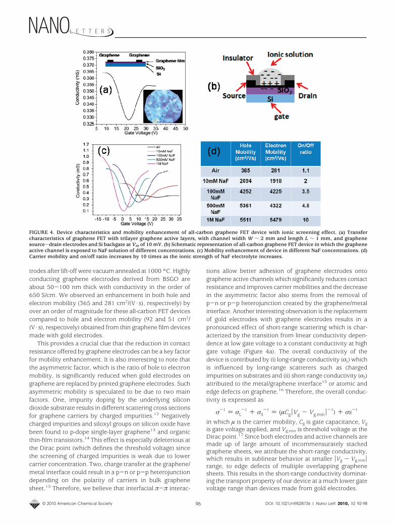
tions allow better adhesion of graphene electrodes ontographene active channels which significantly reduces contactresistance and improves carrier mobilities and the decreasein the asymmetric factor also stems from the removal ofp-n or p-p heterojunction created by the graphene/metalinterface. Another interesting observation is the replacementof gold electrodes with graphene electrodes results in apronounced effect of short-range scattering which is char-acterized by the transition from linear conductivity depen-dence at low gate voltage to a constant conductivity at highgate voltage (Figure 4a). The overall conductivity of thedevice is contributed by (i) long-range conductivity (σL) whichis influenced by long-range scatterers such as chargedimpurities on substrates and (ii) short-range conductivity (σS)attributed to the metal/graphene interface15 or atomic andedge defects on graphene.16 Therefore, the overall conduc-tivity is expressed as
σ-1 ) σL-1 + σS
-1 ) (µCg|Vg - Vg,min|-1) + σs-1
in which µ is the carrier mobility, Cg is gate capacitance, Vg
is gate voltage applied, and Vg,min is threshold voltage at theDirac point.17 Since both electrodes and active channels aremade up of large amount of incommensurately stackedgraphene sheets, we attribute the short-range conductivity,which results in sublinear behavior at smaller |Vg - Vg,min|range, to edge defects of multiple overlapping graphenesheets. This results in the short-range conductivity dominat-ing the transport property of our device at a much lower gatevoltage range than devices made from gold electrodes.
FIGURE 4. Device characteristics and mobility enhancement of all-carbon graphene FET device with ionic screening effect. (a) Transfercharacteristics of graphene FET with trilayer graphene active layers, with channel width W ∼ 2 mm and length L ∼ 1 mm, and graphenesource-drain electrodes and Si backgate at Vds of 10 mV. (b) Schematic representation of all-carbon graphene FET device in which the grapheneactive channel is exposed to NaF solution of different concentrations. (c) Mobility enhancement of device in different NaF concentrations. (d)Carrier mobility and on/off ratio increases by 10 times as the ionic strength of NaF electrolyte increases.
© 2010 American Chemical Society 96 DOI: 10.1021/nl9028736 | Nano Lett. 2010, 10, 92-98
Several possibilities for the types of scatterers as well asscattering mechanisms, which could potentially limit chargecarrier transport, have been discussed in terms of electron-phonon scattering,18 thermal activation barrier of carriers,4
electrostatic screening effect by surface charged impuri-ties,19 graphene ripples (quenched flexural phonons),20 andresonant scatterers.21 The possibility of mobility enhance-ment by the screening of charged impurities on substratesurfaces by applying high ionic strength solutions or highdielectric constant liquids has been demonstrated recentlywith varying degrees of success. Chen et al.19 reported asignificant improvement in the mobility of mechanicallycleaved graphene exposed to high ionic strength solutionswhile Ponomarenko et al.22 reported no significant improve-ment for graphene placed on various substrates in highdielectric constant liquids.
Insights into the main limiting factors in carrier mobil-ity can be obtained by studying the I-Vg characteristicsof a single-layer graphene film versus that of few-layergraphene film. According to our measurements (Figure2b, Figure 2d and Figure 2f), the carrier mobilities of thebilayer and trilayer graphene film are higher than that ofthe single-layer graphene film by ∼10 times. This indi-cates that the main limiting factor is not sheet-to-sheetjunction resistance4 but is dominated by other effects, i.e.,impurity scattering from the SiO2 substrates. Such impu-rity scattering effect will be expected to be more pro-nounced in single-layer graphene film compared to few-layer graphene film due to poorer screening in the formeras a result of lower carrier concentration. Coulomb scat-terers are also expected to be dominant in devices wheremobilities are low in the range of ∼100-1000 cm2/(V·s).22 A verification of the impurity scattering effect canbe seen when we exposed our CPG device to NaF elec-trolytes of different ionic concentrations to investigate thechanges in transfer characteristics in back-gate configu-ration (Figure 4b). The ionic electrolyte provides the ionicscreening needed to nullify the electric field from thenegatively charge impurities on SiO2 substrate.23,24 Re-markably, an improvement by over 1 order of magnitudefor hole and electron mobility (e.g., hole mobility in-creased from 365 to 5511 cm2/(V·s)) and on/off ratio (by10 times) (Figure 4c,d) can be achieved for the CPGdevice. This proves that electrostatic screening effect iscritical for thin graphene films, in which charged carriersin graphene films are insufficient to screen charge impuri-ties on the substrate. In addition, the Dirac point shiftedtoward zero gate voltage with increasing ionic strengthof NaF, thus indicating the screening of electric fieldscreated by charged impurities on SiO2 substrate and thenullification of doping. The reduction of asymmetric factoris also evident from Figure 4c, which can be rationalizedon the basis of the screening of Coulomb scatterers.Therefore, the main scattering mechanism that limits themobility of ultrathin CMG-based device is attributed to
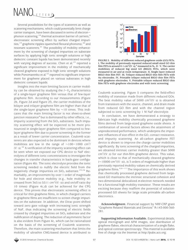
Coulomb scattering. Figure 5 compares the field-effectmobility of transistor made from different reduced GOs.The best mobility value of 5000 cm2/(V·s) is obtainedfrom transistors with the source, channel, and drain madefrom reduced GO film and with the channel regionsubjected to ionic screening by 1 M NaF electrolyte.
In conclusion, we have demonstrated a strategy tofabricate high mobility chemically processed graphenefilms derived from large-sized graphene oxide sheets. Acombination of several factors allows the attainment ofunpredecented performance, which underpins the impor-tant influences of size effect in the GO, contact resistance,and impurity scattering. An all-carbon graphene FETdevice is shown to improve the charge carrier mobilitiessignificantly. By ionic screening of the charged impurities,we obtained intrinsic carrier mobility greater than 5000cm2/(V·s) for our thin-film graphene device. This value,which is close to that of mechanically cleaved graphene(∼10000 cm2/(V·s)), is 3 orders of magnitude higher thanpreviously reported mobility values on chemically derivedgraphene films.4,6-11 The importance of this work showsthat chemically processed graphene derived from large-sized GO maintains the intrinsic structural cohesion andtwo-dimensional delocalized π-electron network neededfor a functional high mobility transistor. These results areexciting because they reaffirm the potential of solution-processed GO sheets for large scale printable all-carbonelectronics.
Acknowledgment. Financial support by NRF-CRP grant“Graphene Related Materials and Devices” R-143-000-360-281.
Supporting Information Available. Experimental details,optical micrograph and AFM images, size distribution ofgraphene flakes, electrical characterization of a single flake,and optical contrast spectroscopy. This material is availablefree of charge via the Internet at http://pubs.acs.org.
FIGURE 5. Mobility of different reduced graphene oxide (GO) FETs.I, The mobility of previously reported reduced small sized GO thinfilm FETs is around 0.1 cm2/(V·s),6 measured in N2. II-V, The carriermobilities of reduced big sized GO (BSGO) FETs, which weremeasured in air and at room temperature. II, Single-layer reducedBSGO thin film FET. III, Trilayer reduced BSGO thin film FETs withAu electrodes. IV, Printable trilayer reduced BSGO thin film FETswith graphene electrodes. V, Printable trilayer reduced BSGO thinfilm FETs with graphene electrodes and with ionic screening.
© 2010 American Chemical Society 97 DOI: 10.1021/nl9028736 | Nano Lett. 2010, 10, 92-98
REFERENCES AND NOTES(1) Gao, W.; Alemany, L. B.; Ci, L.; Ajayan, P. M. Nat. Chem. 2009, 1,
403.(2) Geim, A. K.; Novoselov, K. S. Nat. Mater. 2007, 6, 183.(3) Kim, K. S.; Zhao, Y.; Jang, H.; Lee; Sang Yoon; Kim, J. M.; Kim,
K. S.; Ahn, J.-H.; Kim, P.; Choi, J.-Y.; Hong, B. H. Nature 2009,457, 706.
(4) Eda, G.; Chhowalla, M. Nano Lett. 2009, 9, 814.(5) Becerril, H.; Mao, A.; J, Liu, Z.; Stoltenberg, R. M.; Bao, Z.; Chen,
Y. ACS Nano 2008, 2, 463.(6) Wang, S.; Chia, P.-J.; Chua, L.-L.; Zhao, L.-H.; Png, R.-Q.; Sivara-
makrishnan, S.; Zhou, M.; Goh, R. G-S.; Friend, R. H.; Wee, A. T.-S.; Ho, P. K.-H. Adv. Mater. 2008, 20, 3440.
(7) Eda, G.; Fanchini, G.; Chhowalla, M. Nat. Nanotechnol. 2008, 3,270.
(8) Stankovich, S.; Piner, R. D.; Nguyen, S. T.; Ruoff, R. S. Carbon2006, 44, 3342.
(9) Tung, V. C.; Allen, M. J.; Yang, Y.; Kaner, R. B. Nat. Nanotechnol.2009, 4, 25.
(10) Cote, L. J.; Kim, F.; Huang, J. X. J. Am. Chem. Soc. 2009, 131, 1043.(11) Stankovich, S.; Dikin, D. A.; Piner, R. D.; Kohlhaas, K. A.;
Kleinhammes, A.; Jia, Y. Y.; Wu, Y.; Nguyen, S. T.; Ruoff, R. S.Carbon 2007, 45, 1558.
(12) Novikov, D. S. Appl. Phys. Lett. 2007, 91, 102102.
(13) Casiraghi, C.; Pisana, S.; Novoselov, K. S.; Geim, A. K.; Ferrari,A. C. Appl. Phys. Lett. 2007, 91, 233108.
(14) Chua, L.-L.; Zaumseil, J.; Chang, J.-F.; Ou, E. C.-W.; Ho, P. K.-H.;Sirringhaus, H.; Friend, R. H. Nature 2005, 434, 194.
(15) Huard, B.; Stander, N.; Sulpizio, J. A.; Goldhaber-Gorden, D. Phys.Rev. B. 2008, 78, 121402.
(16) Gass, M. H.; Bangert, U.; Bleloch, A. L.; Wang, P.; Nair, R. R.;Geim, A. K. Nat. Nanotechnol. 2008, 3, 676.
(17) Morozov, S. V.; Novoselov, K. S.; Katsnelson, M. I.; Schedin, F.;Elias, D. C.; Jaszczak, J. A.; Geim, A. K. Phys. Rev. Lett. 2008, 100,No. 016602.
(18) Akturk, A.; Goldsman, N. J. Appl. Phys. 2008, 103, No. 053702.(19) Chen, F.; Xia, J. L.; Tao, N. J. Nano Lett. 2009, 9, 1621.(20) Katsnelson, M. I.; Geim, A. K. Philos. Trans. R. Soc.London, Ser. A
2008, 366, 195. Katsnelson, M. I.; Geim, A. K. Nano Lett. 2008,8, 173.
(21) Wehling, T. O.; Novoselov, K. S.; Morozov, S. V.; Vdovin, E.;Katsnelson, M. I.; Geim, A. K.; Lichtenstein, A. I. Nano Lett. 2008,8, 173.
(22) Ponomarenko, L. A.; Yang, R.; Mohiuddin, T. M.; Katsnelson, M. I.;Novoselov, K. S.; Morozov, S. V.; Zhukov, A. A.; Schedin, F.; Hill,E. W.; Geim, A. K. Phys. Rev. Lett. 2009, 102, 206603.
(23) Edmonds, D. T. Eur. Biophys. J. 1988, 16, 255.(24) Fowkes, F. M.; Burgess, T. E. Surf. Sci. 1969, 13, 184.
© 2010 American Chemical Society 98 DOI: 10.1021/nl9028736 | Nano Lett. 2010, 10, 92-98