Tilburg University The flexible accelerator mechanism in a ...

electronics
Article
High Level Design of a Flexible PCA HardwareAccelerator Using a New Block-Streaming Method
Mohammad Amir Mansoori * and Mario R. Casu
Department of Electronics and Telecommunications, Politecnico di Torino, 10129 Turin, Italy;[email protected]* Correspondence: [email protected]
Received: 3 February 2020; Accepted: 4 March 2020; Published: 7 March 2020�����������������
Abstract: Principal Component Analysis (PCA) is a technique for dimensionality reduction thatis useful in removing redundant information in data for various applications such as MicrowaveImaging (MI) and Hyperspectral Imaging (HI). The computational complexity of PCA has made thehardware acceleration of PCA an active research topic in recent years. Although the hardware designflow can be optimized using High Level Synthesis (HLS) tools, efficient high-performance solutionsfor complex embedded systems still require careful design. In this paper we propose a flexible PCAhardware accelerator in Field-Programmable Gate Arrays (FPGA) that we designed entirely in HLS.In order to make the internal PCA computations more efficient, a new block-streaming method isalso introduced. Several HLS optimization strategies are adopted to create an efficient hardware.The flexibility of our design allows us to use it for different FPGA targets, with flexible input datadimensions, and it also lets us easily switch from a more accurate floating-point implementationto a higher speed fixed-point solution. The results show the efficiency of our design compared tostate-of-the-art implementations on GPUs, many-core CPUs, and other FPGA approaches in terms ofresource usage, execution time and power consumption.
Keywords: FPGA; Principal Component Analysis (PCA); High Level Synthesis (HLS); hardwareacceleration; embedded systems; fixed-point implementation
1. Introduction
Principal Component Analysis (PCA) is a widely-used method for reducing dimensionality.It extracts from a set of observations the Principal Components (PCs) that correspond to the maximumvariations in the data. By projecting the data on an orthogonal basis of vectors corresponding to thefirst few PCs obtained with the analysis and removing the other PCs, the data dimensions can bereduced without a significant loss of information. Therefore, PCA can be used in various applicationswhen there is redundant information in the data. For example, in Microwave Imaging (MI), PCA isuseful before image reconstruction to reduce data dimensions in microwave measurements [1–3]. In arecent work [4], PCA is used as a feature extraction step prior to tumor classification in MI-based breastcancer detection.
PCA involves various computing steps consisting of complex arithmetic operations, which resultin a high computational cost and so a high execution time when implementing PCA in software.To tackle this problem, hardware acceleration is often used as an effective solution that helps reducethe total execution time and enhance the overall performance of PCA.
The main computing steps of PCA, which will be described thoroughly in the next section,include the computation of an often large covariance matrix, which stresses the I/O of hardwaresystems, and the computation of the singular values of the matrix. Since the covariance matrix issymmetric, the singular values are also the eigenvalues and can be computed either with Eigenvalue
Electronics 2020, 9, 449; doi:10.3390/electronics9030449 www.mdpi.com/journal/electronics

Electronics 2020, 9, 449 2 of 23
Decomposition (EVD) or with Singular Value Decomposition (SVD): the more appropriate algorithmto implement in hardware is chosen depending on the application and the performance requirements.Other important steps in PCA are the data normalization, which requires to compute the data mean,and the projection of the data on the selected PCs.
In recent years, numerous hardware accelerators have been proposed that implement either PCAin its entirety or some of its building blocks. For example, in [5] different hardware implementationsof EVD were compared and analyzed on CPU, GPU, and Field-Programmable Gate Arrays (FPGA),and it was shown that FPGA implementations offer the best computational performance, while theGPU ones require less design effort. A new FPGA architecture for EVD computation of polynomialmatrices was presented in [6], in which the authors show how the Xilinx System Generator tool canbe used to increase the design efficiency compared to traditional RTL manual coding. Leveraginga higher abstraction level to improve the design efficiency is also our goal, which we pursue usingthe High-Level Synthesis (HLS) design approach, as we discuss later, as opposed to VHDL- orVerilog-based RTL coding. Wang and Zambreno [7] introduce a floating-point FPGA design of SVDbased on the Hestenes-Jacobi algorithm. Other hardware accelerators for EVD and SVD were proposedin [8–11].
In [12] an embedded hardware was designed in FPGA using VHDL for the computation ofMean and Covariance matrices as two components of PCA. Fernandez et al. [13] presented a manualRTL design of PCA for Hyperspectral Imaging (HI) in a Virtex7 FPGA. The Covariance and Meancomputations could not be implemented in hardware due to the high resource utilization. Das et al. [14]designed an FPGA implementation of PCA in a network intrusion detection system, in whichthe training phase (i.e., computing the PCs) was done offline and only the mapping phase (i.e.,the projection of the data on the PC base) in the online section was accelerated in hardware. Our goalis instead to provide a complete PCA implementation, which can be easily adapted to the availableFPGA resources thanks to the design flexibility enabled by the HLS approach.
Recently, some FPGA accelerators have been introduced that managed to implement a completePCA algorithm. In [15] such an accelerator was designed in a Virtex7 FPGA using VHDL, but it isapplicable only to relatively small matrix dimensions. Two block memories were used for the internalmatrix multiplication to store the rows and columns of the matrices involved in the multiplication,which resulted in a high resource usage. Thanks to our design approach, instead, we are able toimplement a complete PCA accelerator for large matrices even with few FPGA resources.
FPGAs are not the only possible target for PCA acceleration. In [16], all the PCA componentswere implemented on two different hardware platforms, a GPU and a Massively Parallel ProcessingArray (MPPA). Hyperspectral images with different dimensions were used as test inputs to evaluatethe hardware performance. It is well known, however, that these kinds of hardware acceleratorsare not as energy-efficient as FPGAs. Therefore we do not consider them, especially because ourtarget computing devices are embedded systems in which FPGAs can provide an efficient way forhardware acceleration.
To design a hardware accelerator in FPGA, the traditional approach uses Hardware DescriptionLanguages (HDL) like VHDL or Verilog. Although this approach is still the predominant designmethodology, it increases the development time and the design effort. As embedded systemsare becoming more complex, designing an efficient hardware in RTL requires significant effort,which makes it difficult to find the best hardware architecture. An alternative solution that is becomingmore popular in recent years is the High Level Synthesis (HLS) approach. HLS raises the designabstraction level by using software programming languages like C or C++. Through the processesof scheduling, binding, and allocation, HLS converts a software code into its corresponding RTLdescription. The main advantage of HLS over HDL is that it enables designers to explore the designspace more quickly, thus reducing the total development time with a quality of results comparableand often better than RTL design. Another important advantage is the flexibility, which we use in

Electronics 2020, 9, 449 3 of 23
this work and which allows designers to use a single HLS code for different hardware targets withdifferent resource and performance constraints.
Recently, HLS-based accelerators have been proposed for PCA. In [17], a design based on HLSwas introduced for a gas identification system and implemented on a Zynq SoC. Schellhorn et al.,presented in [18] another PCA implementation on FPGA using HLS for the application of spectralimage analysis, in which the EVD part could not be implemented in hardware due to the limitedresources. In [19], we presented an FPGA accelerator by using HLS to design the SVD and projectionbuilding blocks of PCA. Although it could be used for relatively large matrix dimensions, the otherresource-demanding building blocks (especially covariance computation) were not included in thatdesign. In a preliminary version of this work [20], we proposed another HLS-based PCA acceleratorto be used with flexible data dimensions and precision, but limited in terms of hardware target to alow-cost Zynq SoC and without the support for block-streaming needed to handle large data matricesand covariance matrices, which instead we show in this paper.
The PCA hardware accelerators proposed in the literature have some drawbacks. The manualRTL approach used to design the majority of them is one of the disadvantages, which leads toan increase in the total development time. Most of the previous works, including some of theHLS-based designs, could not implement an entire PCA algorithm including all the computationalunits. Other implementations could not offer a flexible and efficient design with a high computationalperformance that could be used for different data sizes.
In this paper we close the gap in the state of the art and propose an efficient FPGA hardwareaccelerator that has the following characteristics:
• The PCA algorithm is implemented in FPGA in its entirety.• It uses a new block-streaming method for the internal covariance computation.• It is flexible because it is entirely designed in HLS and can be used for different input sizes and
FPGA targets.• It can easily switch between floating-point and fixed-point implementation, again thanks to the
HLS approach.• It can be easily deployed on various FPGA-based boards, which we prove by targeting both a
Zynq7000 and a Virtex7 in their respective development boards.
The rest of the paper is organized as follows. At first, in Section 2 the PCA algorithm is describedwith the details of its processing units. We briefly describe in Section 3 the application of PCA toHyperspectral Imaging (HI), which we use as a test case to report our experimental results and tocompare them with previously reported results. The proposed PCA hardware accelerator and theblock-streaming method is presented in Section 4 together with the HLS optimization techniques.The implementation results and the comparisons with other works are reported in Section 5. Finally,the conclusions are drawn in Section 6.
2. PCA Algorithm Description
Let X be an array of size R× C in which R (Rows) is the number of data samples and C (Columns)is the main dimension in which there is redundant information. PCA receives X and produces alower-dimensionality array Y of size R× L with L < C through the steps shown in Algorithm 1.
In the first step, the mean values of each column of the input data are computed and storedin matrix M for data normalization. The second step is the computation of the covariance of thenormalized data, which is one of the most computationally expensive steps of PCA due to the largenumber of multiplications and additions. After computing the eigenvalues or singular values (andthe corresponding eigen/singular vectors) of the covariance matrix by using EVD or SVD in thethird step, they are sorted in descending order and the first L eigen/singular vectors are selected as

Electronics 2020, 9, 449 4 of 23
Principal Components in the fourth step. The selection of PCs is based on the cumulative energy ofeigen/singular values. After computing the total energy (E) as in the following equation,
E =C
∑i=1
σi, (1)
where σi is the energy of the ith eigen/singular value, the first L components are selected in such away that their cumulative energy is no less than a predetermined fraction of total energy, the thresholdT (%), as follows:
100× ∑Li=1 σi
E≥ T. (2)
Finally, in the last step, the normalized input is projected into the principal components space toreduce the redundant information.
Algorithm 1: PCA algorithmStep 1- Mean computation: /* MR×C is the matrix representation of vector Mean1×C */[Mean]1×C = 1
R ∑Ri=1[Xi]1×C /* [X]i is the ith row of the input matrix XR×C */
MR×C : [Mi]1×C = [Mean]1×C, i = 1, 2, ..., R /* [Mi] is the ith row of matrix M*/Step 2- Covariance calculation:[COV]C×C = 1
R−1 (X−M)T × (X−M)
Step 3- EVD/SVD of covariance:COV = UΣUT
Step 4- Sort and selection:Σs, Us = Sort(Σ, U)
[PC]C×L = Select(Σs, Us)
Step 5- Projection:[Y]R×L = (X−M)× PC
3. Hyperspectral Imaging
Although we are interested in the application of PCA to Microwave Imaging (MI), to the best ofour knowledge there is no hardware accelerator for PCA in the literature that is specifically aimed atsuch application. In order to compare our proposed hardware with state-of-the-art PCA accelerators,we had to select another application for which an RTL- or HLS-based hardware design was available.Therefore, we selected the Hyperspectral Imaging (HI) application.
Hyperspectral Imaging (HI) sensors acquire digital images in several narrow spectral bands.This enables the construction of a continuous radiance spectrum for every pixel in the scene. Thus,HI data exploitation helps to remotely identify the ground materials-of-interest based on their spectralproperties [21].
HI data are organized in a matrix of size R× C in which R is the number of pixels in the imageand C is the number of spectral bands. Usually, there is redundant information in different bands thatcan be removed with PCA. In the following notations, we use interchangeably the terms R(Rows) andpixels, as well as C(Columns) and bands.
For MI, instead, the R× C matrix could represent data gathered in C different frequencies in themicrowave spectrum by R antennas, or a reconstructed image of the scattered electromagnetic field ofR pixels also at C frequencies.
4. PCA Hardware Accelerator Design
Figure 1 shows the architecture of the PCA accelerator and its main components. Since theaccelerator is developed in HLS using C++, the overall architecture correspond to a C++ function andits components correspond to subfunctions. At the highest level, there are two subfunctions named

Electronics 2020, 9, 449 5 of 23
Dispatcher and PCA core. The Dispatcher reads the input data stored in an external DDR memoryand sends them to the PCA core through the connecting FIFOs. The connection with FIFOs is alsodescribed in HLS with proper code pragmas.
Figure 1. Architecture of the proposed hardware accelerator for Principal Component Analysis (PCA)in Field-Programmable Gate Arrays (FPGA).
The PCA core contains different processing units. The first is the Mean unit, which computesthe mean vector corresponding to the mean value of each column of the input matrix. This vector isstored in an internal memory that is used by the next processing units, Cov and PU, for data centering.The Cov unit uses the new block-streaming method for computing the covariance matrix, which willbe explained thoroughly in the following subsection. It reads the required data from two sets of FIFOscorresponding to diagonal and off-diagonal computation. Then the SVD unit computes the singularvalues of the covariance matrix, and the Sort and Select unit sorts them and retains the first components.Finally, the Projection unit reads the input data again and computes the multiplication between thecentered data and the sorted and selected PCs to produce the final PCA output data, which are writtenback to the external DDR memory.
The computational cost of PCA depends on the input dimensions. When the main dimensionfrom which the redundant information must be removed (columns or bands in HI) is lower than theother dimension (rows or pixels in HI), the PCA performance is mainly limited by the computation ofthe covariance matrix, due to the large number of multiplications and additions that are proportionalto the number of pixels. Indeed, in the covariance computation all the pixels in one band must bemultiplied and accumulated with the corresponding pixels in all of the bands. This is illustrated inFigure 2 where the bands are specified by the letters α to n and pixels are indicated by the indices 1 toN. The result of the covariance computation, which is the output of the Cov unit, is a matrix of size(bands× bands) that becomes the input of the SVD unit. In HI applications, in which it is true thatpixels� bands, the covariance computation is the major limitation of the whole PCA design, hence itsacceleration can drastically enhance the overall performance.
Multiple parallel streaming FIFOs are needed to match the parallelism of the accelerated Cov unit.The number of FIFOs is determined based on the input data dimensions and the maximum bandwidthof the external memory. Streaming more data at the same time through the FIFOs enables a degreeof parallelism that is matched to the number of columns of the input matrix. It is important to notethat all of the hardware components are described in a single HLS top-level function, which simplifiesthe addition of different flexibility options to the design such as variable data dimensions, block sizes,and number of FIFOs.

Electronics 2020, 9, 449 6 of 23
The complexity of the Cov unit compared to other parts raises the importance of theblock-streaming method in covariance computation as this method allows using the same designfor higher data dimensions or improving the efficiency in low-cost embedded systems with fewerhardware resources.
Figure 2. Example of covariance computation with 9 bands and N pixels, PQ = ΣNi=1Pi ×Qi, where P, Q
are the symbols of bands (α to n).
4.1. Block-Streaming for Covariance Computation
The block-streaming method is helpful whenever there is a limitation in the maximum size ofinput data that can be stored in an internal memory in the Cov unit. Therefore, instead of streamingthe whole data one time, we stream “blocks” of data several times through the connecting FIFOs.There are two internal memories inside the Cov unit each of which can store a maximum number ofbands (Bmax) for each pixel. These memories are used in the diagonal and off-diagonal computations,so we call them “Diag” and “Off-diag” RAMs, respectively. The input data is partitioned into severalblocks along the main dimension (bands) with a maximum dimension of Bmax (block size). Each blockof data is streamed through the two sets of FIFOs located between the Dispatcher and Cov unit (Diagand Off-diag FIFOs) in a specific order, and after the partial calculation of all the elements of thecovariance matrix for one pixel, the data blocks for the next pixels will be streamed and the partialresults accumulated together to obtain the final covariance matrix.
To better understand the block-streaming method, we provide two examples in Figures 3–6.
Figure 3. Example of partitioning of input data into blocks. The total number of bands is B = 9 and theblock size is Bmax = 3.

Electronics 2020, 9, 449 7 of 23
Figure 4. Illustration of an example of covariance computation using the block-streaming method with3 blocks (B = 9, Bmax = 3).
The first example is illustrated in Figure 3 in which the total number of bands is B = 9 and theblock size is Bmax = 3. Therefore, we have 3 blocks of data that are specified in figure as P1 to P3.The Block-streaming method consists of the following steps that can be realized from Figure 4:
1. Diagonal computation:
The 3 blocks of data (P1 to P3) for the first pixel are streamed in Diag FIFOs one by one and afterstorage in the Diag RAM, the diagonal elements P11, P22, and P33 are computed.
2. Off-diagonal computation of the last block:
(a) Keep the last block (P3) in the Diag RAM.(b) Stream the first block (P1) into Off-Diag FIFOs, store it in Off-Diag RAM, and compute
P13 = P1× P3.(c) Stream the second block (P2) into Off-Diag FIFOs, store it in Off-Diag RAM, and compute
P23 = P2× P3.
3. Off-diagonal computation of the preceding blocks:
(a) Update the Diag RAM by the last values of Off-Diag RAM (P2).(b) Stream the first block (P1) into Off-Diag FIFOs, store it in Off-Diag RAM, and compute
P12 = P1× P2.
4. Stream Pixels: Steps 1 to 3 are repeated for the next pixels and the results are accumulated toobtain the final covariance matrix.
The second example is illustrated in Figure 5 in which the number of blocks is 4 and after thediagonal computation (in green color) there are 3 steps for off-diagonal computations that are indicatedin 3 different colors. Figure 6 shows the order of data storage in the Diag and Off-diag RAMs. After the7th and 9th steps, the Diag RAM is updated by the last value of Off-Diag RAM (P3 and P2).
Figure 5. Block-streaming method with 4 blocks (B/Bmax = 4).

Electronics 2020, 9, 449 8 of 23
Figure 6. Order of data storage in the Diagonal and Off-diagonal RAMs inside the Cov unit.
4.2. High Level Synthesis Optimizations
4.2.1. Tool Independent Optimization Directives and Their Hardware Implementation
To introduce the principles behind the hardware optimization techniques used in the proposeddesign, a more abstract description of the high-level directives is presented in this part withoutreferences to a specific hardware design tool. In Figure 7 the most widely used optimization directivesare illustrated with their corresponding hardware implementation. These directives are Loop Pipelining,Loop Unrolling, Array Partitioning, and Dataflow.
Loop Pipelining allows multiple operations of a loop to be executed concurrently by using thesame hardware iteratively. Loop Unrolling creates multiple instances of the hardware for the loop body,which allows some or all of the loop iterations to occur in parallel. By using Array Partitioning we cansplit an array, which is implemented in RTL by default as a single block RAM resource, into multiplesmaller arrays that are mapped to multiple block RAMs. This increases the number of memory portsproviding more bandwidth to access data. Finally, the Dataflow directive allows multiple functions orloops to operate concurrently. This is achieved by creating channels (FIFOs or Ping-Pong buffers) inthe design, which enables the operations in a function or loop to start before the previous function orloop completes all of its operations. Dataflow directive is mainly used to improve the overall latencyand throughput of the design. Latency is the time required to produce the output after receiving theinput. Throughput is the rate at which the outputs are produced (or the inputs are consumed) and ismeasured as the reciprocal of the time difference between two consecutive outputs (or inputs).
Figure 7. Hardware optimization directives.
Electronics 2020, 9, 449 9 of 23
The PCA hardware accelerator is designed in C++ using Vivado HLS, the HLS developmenttool for Xilinx FPGAs. The above-mentioned optimization directives can be applied easily in HLS byusing their corresponding code pragmas. HLS enables us to specify the hardware interfaces as wellas the level of parallelism and pipelined execution and specific hardware resource allocation thanksto the addition of code pragmas. By exploring different combinations of the optimization directives,it is possible to determine relatively easily the best configuration in terms of latency and resourceusage. Therefore, several interface and hardware optimization directives have been applied in the HLSsynthesis tool, as explained below.
4.2.2. Input Interfaces
The main input interface associated to the Dispatcher input and the output interface associated tothe PU output consist of AXI master ports, whose number and parallelism are adapted to the FPGAtarget. For the Zynq of the Zedboard, four AXI ports (with a fixed width of 64 bits) are connected tothe Dispatcher input in such a way to fully utilize the available memory bandwidth. In the Virtex7of the VC709 board we can use instead only one AXI port with a much larger bit-level parallelism.The output interface for both boards is one AXI master port that is responsible for writing the output tothe memory. Other interfaces are specified as internal FIFOs between the Dispatcher and the PCA core.As shown in Figure 1, four sets of FIFOs send the streaming data (containing a data block of bands)from the Dispatcher to the corresponding processing units in the PCA core. Mean and Projection unitsreceive two sets of FIFOs and Cov unit receives another two. Each set of FIFOs is partitioned by Bmax,the size of a data block, so that there are Bmax FIFOs in each set.
These FIFOs are automatically generated by applying the Vivado HLS Dataflow directive for theconnection between the Dispatcher and the PCA core. This directive lets the two functions executeconcurrently and their synchronization is made possible by the FIFO channels automatically insertedbetween them.
4.2.3. Code Description and Hardware Optimizations
In this part the code description for each PCA component is presented. To optimize the hardwareof each PCA unit, we analyzed the impact of different HLS optimizations on the overall performance.Specifically, we considered the impact of loop pipelining, loop unrolling, and array partitioning onlatency and resource consumption. The best HLS optimizations are selected in such a way that theoverall latency is minimized by utilizing as many resources as required.
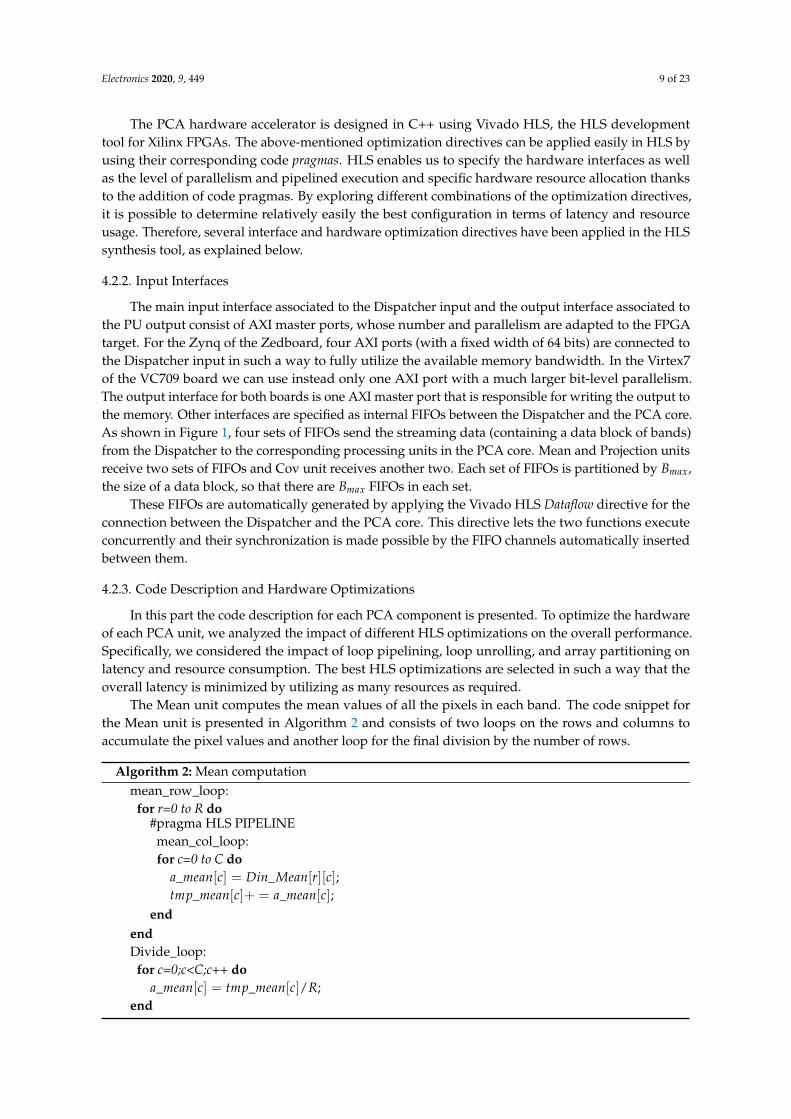
The Mean unit computes the mean values of all the pixels in each band. The code snippet forthe Mean unit is presented in Algorithm 2 and consists of two loops on the rows and columns toaccumulate the pixel values and another loop for the final division by the number of rows.
Algorithm 2: Mean computationmean_row_loop:for r=0 to R do
#pragma HLS PIPELINEmean_col_loop:for c=0 to C do
a_mean[c] = Din_Mean[r][c];tmp_mean[c]+ = a_mean[c];
endendDivide_loop:for c=0;c<C;c++ do
a_mean[c] = tmp_mean[c]/R;end

Electronics 2020, 9, 449 10 of 23
The best HLS optimization for the Mean unit is to pipeline the outer loop (line #pragma HLSPIPELINE in Algorithm 2), which reduces the Initiation Interval (II), i.e., the index of performance thatcorresponds to the minimum time interval (in clock cycles) between two consecutive executions of theloop (ideally, II = 1). In addition, the memory arrays a_mean and tmp_mean are partitioned by Bmax
(not shown in the code snippet) to have access to multiple memory locations at the same time, which isrequired for the loop pipelining to be effective, otherwise the II will increase due to the latency neededto access a single, non-partitioned memory.
The Cov unit uses the block-streaming method to compute the covariance matrix. Its pseudo codeis presented in Algorithm 3. The HLS optimizations include loop pipelining, unrolling, and the arraysfull partitioning. In Algorithm 3 full indexing is not displayed to make the code more readable andonly the relation between the variables and the indexes is shown by the parentheses. For example,DiagFIFO(r,b) indicates that the indexes of variable DiagFIFO are proportional to (r,b). The standardCov computation is adopted from [20] and is used for diagonal covariance computations. The writefunction in the last line writes the diagonal and off-diagonal elements of covariance matrix fromvariables CovDiag and CovOff to the corresponding locations in CovOut. As shown in Algorithm 3,there are two pipeline directives that are applied to the loops on the diagonal and off-diagonal blocks,respectively. The memory arrays need to be fully partitioned, which is required to unroll the innerloops. As described before, a thorough analysis of different possible optimizations was performed tofind out a trade-off between resource usage and latency.
Algorithm 3: Cov computation, block-streaming
for r=0 to R do /* Stream Pixels */for b=0 to NB do /* Diagonal Computations, NB = B/Bmax */
#pragma HLS PIPELINEDiagRAM = DiagFIFO(r, b)− a_mean(b);/* Start standard Cov computation [20] */for c1=0 to Bmax do
for c2=c1 to Bmax do.../* indexing */CovDiag(b, Index) = DiagRAM[c1] ∗ DiagRAM[c2];
endend/* Finish standard Cov computation */
endfor ct=1 to NB do /* Off-Diagonal computations */
for b=0 to NB-ct do#pragma HLS PIPELINEif Step3(a) then /*refer to Section 4.1, the four steps of block-streaming method*/
DiagRAM = O f f RAM;endO f f RAM = O f f FIFO(r, b)− a_mean(b);CovO f f (b, ct)+ = O f f RAM ∗ DiagRAM;
endend
end/* Write to the final Cov matrix */CovOut = write(CovDiag, CovO f f );
The next processing unit is the EVD of the covariance matrix. For real and symmetric matrices(like the covariance matrix) EVD is equal to SVD and both methods can be used. For SVD computation

Electronics 2020, 9, 449 11 of 23
of floating-point matrices, there is a built-in function in Vivado HLS that is efficient especially forlarge dimensions. On the other hand, a fixed-point implementation of EVD is highly beneficial forembedded systems due to the lower resource usage (or better latency) compared to the floating-pointversion of the same design.
For these reasons, in this paper we propose two versions of the PCA accelerator. The first one is thefloating-point version, which uses the built-in HLS function for SVD computation. The second one isthe fixed-point version, which uses the general two-sided Jacobi method for EVD computation [22,23].The details of this method for computing EVD is shown in Algorithm 4. As we will show in theresults section, there is no need to add any HLS optimization directives to the fixed-point EVD (for ourapplication) because the overall latency of the PCA core, which includes EVD, is lower than the datatransfer time, so there is no benefit in consuming any further resources to optimize the EVD hardware.We do not report the code of the floating-point version as it uses the built-in Vivado HLS function forSVD (Vivado Design Suite User Guide: High-Level Synthesis, UG902 (v2019.1), Xilinx, San Jose, CA,2019 https://www.xilinx.com/support/documentation/sw_manuals/xilinx2019_1/ug902-vivado-high-level-synthesis.pdf).
Algorithm 4: EVD computation, Two-sided Jacobi method/*Initialize the eigenvector matrix V and the maximum iterations max = bands*/V = I; /* I is the identity matrix */for l=1 to max do
for all pairs i<j do
/* Compute the Jacobi rotation which diagonalizes
[Hii HijHji Hjj
]=
[a cc b
]*/
τ = (b− a)/(2 ∗ c); t = sign(τ)/(|τ|+√
1 + τ2);cs = 1/
√1 + t2;sn = cs ∗ t;
/* update the 2× 2 submatrix */Hii = a− c ∗ t;Hjj = b + c ∗ t;Hij = Hji = 0;/* update the rest of rows and columns i and j */for k=1 to bands except i and j do
tmp = Hik;Hik = cs ∗ tmp− sn ∗ Hjk;Hjk = sn ∗ tmp + cs ∗ Hjk;Hki = Hik; Hkj = Hjk;
end/* update the eigenvector matrix V /*for k=1 to bands do
tmp = Vki;Vki = cs ∗ tmp− sn ∗Vkj;Vkj = sn ∗ tmp + cs ∗Vkj;
endend
end
The last processing unit is the Projection Unit (PU), which computes the multiplication betweenthe centered data and the principal components. Algorithm 5 presents the code snippet for the PU.Similar to the Mean unit, we applied some optimizations to this code. The second loop is pipelinedand, as a consequence, all the inner loops are unrolled. In addition, the memory arrays involved in the

Electronics 2020, 9, 449 12 of 23
multiplication must be partitioned. For more information on the hardware optimizations for Meanand PU and their impact on the latency and resource usage please refer to [20].
Algorithm 5: Projection computation
for r=0 to R dofor c1=0 to L do
#pragma HLS PIPELINEtmp = 0;
for n=0 to C do.../* Index control */Din_Nrml[n] = Din_PU[r][n]− a_mean[n];
endfor c2=0 to C do
tmp+ = (Din_Nrml[c2] ∗ PC[c2][c1];endData_Trans f ormed[r][c1] = tmp;
endend
4.3. Fixed-Point Design of the Accelerator
There are many considerations when selecting the best numerical representation (floating- orfixed- point) in digital hardware design. Floating-point arithmetic is more suited for applicationsrequiring high accuracy and high dynamic range. Fixed-point arithmetic is more suited for lowpower embedded systems with higher computational speed and fewer hardware resources. In someapplications, we need not only speed, but also high accuracy. To fulfill these requirements, we canuse a fixed-point design with a larger bit-width. This increases the resource usage to obtain a higheraccuracy, but results in a higher speed thanks to the low-latency fixed-point operations. Therefore,depending on the requirements, it is possible to select either a high-accuracy low-speed floating-point,a low-accuracy high-speed fixed-point, or a middle-accuracy high-speed fixed-point design. Availableresources in the target hardware determine which design or data representation is implementable onthe device. In high-accuracy high-speed applications, we can use the fixed-point design with a highresource usage (even more than the floating-point) to minimize the execution time.
To design the fixed-point version of the PCA accelerator, the computations in all of the processingunits must be in fixed-point. The total Word Length (WL) and Integer Word Length (IWL) must bedetermined for every variable. The range of input data and the data dimensions affect the word lengthsin fixed-point variables, so the fixed-point design may change depending on the data set.
For our HI data set with 12 bands, we used the MATLAB fixed-point converter to optimize theword lengths. In HLS we selected the closest word lengths to the MATLAB ones because some HLSfunctions do not accept all the fixed-point representations (for example in the fixed-point square rootfunction, IWL must be lower than WL).
The performance of EVD/SVD depends only on the number of bands. As we will see in the nextsection, the latency of our EVD design in HLS is significantly higher than the HLS built-in SVD functionfor floating-point inputs. One possible countermeasure is to use the SVD as the only floating-pointcomponent in a fixed-point design to obtain better latency, by adding proper interfaces for data-typeconversion. However, when the data transfer time (i.e., the Dispatcher latency) is higher than the PCAcore latency, the fixed-point EVD is more efficient because of the lower resource usage, which is thecase for a small number of bands.
Electronics 2020, 9, 449 13 of 23
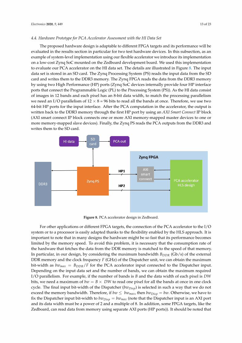
4.4. Hardware Prototype for PCA Accelerator Assessment with the HI Data Set
The proposed hardware design is adaptable to different FPGA targets and its performance will beevaluated in the results section in particular for two test hardware devices. In this subsection, as anexample of system-level implementation using our flexible accelerator we introduce its implementationon a low-cost Zynq SoC mounted on the Zedboard development board. We used this implementationto evaluate our PCA accelerator on the HI data set. The details are illustrated in Figure 8. The inputdata set is stored in an SD card. The Zynq Processing System (PS) reads the input data from the SDcard and writes them to the DDR3 memory. The Zynq FPGA reads the data from the DDR3 memoryby using two High Performance (HP) ports (Zynq SoC devices internally provide four HP interfaceports that connect the Programmable Logic (PL) to the Processing System (PS)). As the HI data consistof images in 12 bands and each pixel has an 8-bit data width, to match the processing parallelismwe need an I/O parallelism of 12 × 8 = 96 bits to read all the bands at once. Therefore, we use two64-bit HP ports for the input interface. After the PCA computation in the accelerator, the output iswritten back to the DDR3 memory through the first HP port by using an AXI Smart Connect IP block(AXI smart connect IP block connects one or more AXI memory-mapped master devices to one ormore memory-mapped slave devices). Finally, the Zynq PS reads the PCA outputs from the DDR3 andwrites them to the SD card.
Figure 8. PCA accelerator design in Zedboard.
For other applications or different FPGA targets, the connection of the PCA accelerator to the I/Osystem or to a processor is easily adapted thanks to the flexibility enabled by the HLS approach. It isimportant to note that in many designs the hardware might be so fast that its performance becomeslimited by the memory speed. To avoid this problem, it is necessary that the consumption rate ofthe hardware that fetches the data from the DDR memory is matched to the speed of that memory.In particular, in our design, by considering the maximum bandwidth BDDR (Gb/s) of the externalDDR memory and the clock frequency F (GHz) of the Dispatcher unit, we can obtain the maximumbit-width as bwmax = BDDR/F for the PCA accelerator input connected to the Dispatcher input.Depending on the input data set and the number of bands, we can obtain the maximum requiredI/O parallelism. For example, if the number of bands is B and the data width of each pixel is DWbits, we need a maximum of bw = B× DW to read one pixel for all the bands at once in one clockcycle. The final input bit-width of the Dispatcher (bwDisp) is selected in such a way that we do notexceed the memory bandwidth. Therefore, if bw ≤ bwmax, then bwDisp = bw. Otherwise, we have tofix the Dispatcher input bit-width to bwDisp = bwmax (note that the Dispatcher input is an AXI portand its data width must be a power of 2 and a multiple of 8. In addition, some FPGA targets, like theZedboard, can read data from memory using separate AXI ports (HP ports)). It should be noted that

Electronics 2020, 9, 449 14 of 23
all the above-mentioned conditions can be easily described in HLS using a set of variables and C++macros that are set at the design time. In order to map the design into a new FPGA target, the onlyrequired change is to adjust the pre-defined variables based on the hardware device.
5. Results
The proposed PCA accelerator is implemented using Vivado HLS 2019.1. To demonstrate theflexibility of the proposed method, we did the experiments on two Xilinx FPGA devices and theirdevelopment boards, the relatively small Zynq7000 (XC7z020clg484-1) on a Zedboard and the largeVirtex7 (XC7vx690tffg1761-2) on a VC709 board. The results are evaluated for different numbersof bands, blocks and pixels. In addition, for the smaller FPGA with limited resources, we report acomparison between the fixed-point and the floating-point versions of the accelerator. Finally, the HIdata set is used to evaluate the performance of the PCA accelerator in the Zynq device. Accuracy,execution time, and power consumption are also measured for both floating- and fixed-point design.Note that we define the execution time or latency as the period of time between reading the first inputdata from the external memory by the Dispatcher and writing the last PCA output to the memory bythe Projection unit.
In the following subsections the impact of input dimensions (bands and pixels), size of the blocks(Bmax in the block-streaming method), and data format (floating- or fixed-point) on the resource usageand latency is evaluated for the two hardware devices.
5.1. Number of Blocks, Bands, and Pixels
To show the efficiency of the trade-off between latency and resources enabled by theblock-streaming method, different numbers of bands and blocks are considered. In the first experimentwith the floating-point version on the Virtex7, we consider the total number of bands set at 48and the size of the block (Bmax) as a parameter that changes from 4 to 16. Figure 9 shows that,as expected, by using a larger block the total latency decreases in exchange for an increase in theresource usage. The latency for different parts of the accelerator is shown with different colors.The most time-consuming parts are Cov and Dispatcher (Dispatcher latency is the time for datatransfer through the FIFOs). By increasing the block size (when Bmax = 16) we can reduce the latencyof Cov computation, so that the only limitation becomes the Dispatcher latency. It should be notedthat the PCA core and the Dispatcher work concurrently, which reduces the overall latency of theentire design.
Figure 9. Impact of block size (Bmax) on the resource usage and latency for the Virtex7, bands = 48,pixels = 300× 300, floating-point design.
Increasing the number of pixels changes the latency of the design as the time to stream the wholedata increases. Figure 10 shows the latency of different parts of the design when changing the totalnumber of pixels. The resource consumption remains constant and does not change with the number

Electronics 2020, 9, 449 15 of 23
of pixels. As expected, the latency of SVD is also constant because it depends on the number of bands,not on the number of pixels. For the other parts, the latency increases almost proportionally.
Figure 10. Impact of the number of pixels on the latency for Virtex7, bands = 48, Bmax = 8,floating-point design.
In the next experiment the block size is fixed to Bmax = 8 and the total number of bands is variable.The resource usage in the Virtex7 for the floating-point version of the PCA core without the SVD part(PCA-SVD), and the latency for different bands with a fixed Bmax are shown in Figure 11. The numberof pixels in this case is 300× 300. The number of bands has a direct impact on the generated SVDhardware, so the resource usage of SVD unit is excluded from the total resources to obtain a betterestimate of the performance of the block-streaming method.
Figure 11. Latency and resource usage for Virtex7 with a fixed block size (Bmax = 8),floating-point design.
As shown in Figure 11, the latency increases with the number of bands because the computationaltime depends on the main dimension. From the resource usage, it is evident that the FFs, DSPs,and LUTs are almost constant (except for a slight increase due to other components of PCA core likeMean and PU). The number of BRAMs, however, increases because in the HLS design there are othertwo memory arrays in addition to Diagonal and Off-diagonal RAMs to store the temporary values ofthe computations (CovDiag and CovOff in Algorithm 3) and the dimensions of these arrays depend onthe ratio between the total bands and Bmax. Still, up to a very large number of bands, the total resourceusage of the most critical component is well below 30%.
5.2. Fixed-Point and Floating-Point Comparison
The fixed-point design of the PCA accelerator is evaluated on the Zynq7000 for different numbersof bands and blocks and is compared with the floating-point design. We first obtained the word

Electronics 2020, 9, 449 16 of 23
lengths using the MATLAB fixed-point converter and then used the nearest possible word lengths inthe HLS design.
The total resource usage for the fixed- and floating-point design is shown in Figure 12 for a fixednumber of bands (B = 12). In the floating-point design (histogram on the left side of Figure 12),the maximum block size is Bmax = 3 because the LUTs required for larger block values exceed the LUTsavailable. For the fixed-point design (histogram on the right side of Figure 12), however, the blocksize can be up to 4. The comparison of the floating- and fixed-point designs for the same block size(Bmax = 3) shows that there is a reduction in the resource usage for the fixed-point design except forthe DSP usage. This is because to obtain a similar accuracy the fixed-point representation requiresa larger bit-width. As a consequence, the HLS design requires more DSPs to implement the sameoperations in fixed-point.
Figure 12. Resource usage for Zedboard for fixed- and floating-point design, B = 12, pixels = 300× 300.
The larger amount of resources needed by fixed-point design is counterbalanced by the lowerlatency, as shown in Figure 13 for B = 12 and Bmax = 3, 4. The fixed-point design has a lower latencyat the same block size and even less latency when using a larger block (Bmax = 4). This is because thelatency of fixed-point operations is lower than the floating-point ones. For example, the fixed-pointadder has a latency of 1 clock cycle, while the floating-point adder has a latency of 5 clock cycles.
Figure 13. Comparison of the latency of the fixed- and floating-point design for Zedboard, B = 12,pixels = 300× 300.
Figures 14 and 15 illustrate the total latency of the PCA accelerator and its resource usage fordifferent numbers of bands for a fixed block size (Bmax = 3). As shown in Figure 14, the latency ofthe floating-point design is limited by the PCA core function, whereas in the fixed-point design theDispatcher latency is the main limitation. This is because the PCA core and the Dispatcher operateconcurrently, as noted before, and therefore the total latency is basically the maximum between the

Electronics 2020, 9, 449 17 of 23
two latencies, which may change depending on the implementation details (in this case floating-versus fixed-point data representation). The comparison of the resource usage in Figure 15 showsthat except for an increase in the DSP usage, other resources are reduced in the fixed-point design.As explained before, the increase in DSP usage is due to the larger bit-width needed for the fixed-pointdata representation.
Figure 14. Latency for Zynq7000 with a fixed block size (Bmax = 3), pixels = 300× 300.
Figure 15. Resource usage for Zynq7000 with a fixed block size (Bmax = 3), pixels = 300× 300.
5.3. Evaluation on Hyperspectral Images
The hyperspectral image data set is obtained from Purdue Research Foundation and is availableonline (https://engineering.purdue.edu/~biehl/MultiSpec/hyperspectral.html). It shows a portionof southern Tippecanoe county, Indiana, and comprises 12 bands each of which corresponds to animage of 949× 220 pixels. We will show that by using PCA, most of the information in the 12 bands isredundant and could be obtained from the first 3 principal components.
The PCA accelerator for this data set is evaluated on the Zynq7000 of the Zedboard for differentpossible block sizes (Bmax = 3, 4). The HLS estimation of the resource usage for the floating- andfixed-point design is indicated in Table 1. For the floating-point design, the maximum block size isBmax = 3. In fixed-point design, however, we can use a larger block size (Bmax = 4), which leads to theincrease in the resource usage.
Table 1. Resource usage obtained from HLS for HI data set on Zedboard, bands = 12.
BRAM (%) DSP (%) FF (%) LUT (%)
floating-point (Bmax = 3) 27 57 33 92fixed-point (Bmax = 3) 23 82 20 75fixed-point (Bmax = 4) 33 99 20 81
Table 2 shows the latency of different components of the design. According to Table 2,the fixed-point minimum latency is about half of the floating-point latency. in addition, the fixed-point

Electronics 2020, 9, 449 18 of 23
EVD latency is about 15 times larger than the floating-point SVD latency. However, this does notaffect the total latency because the Dispatcher latency in the fixed-point design is higher than the PCAcore latency. Therefore, due to the concurrency between Dispatcher and PCA core, the total latency islimited by the Dispatcher. The resource usage for EVD is lower than SVD, so by using the fixed-pointEVD we can improve the overall performance because the resources saved by EVD can be used in therest of the design for more parallelism leading to a lower total latency.
Table 2. Latency (ms) for Zedboard, HI data set, bands = 12.
Total Dispatcher PCA_core SVD/EVD Cov Mean PU
floating-point (Bmax = 3) 296.6981 202.0993 282.9185 0.399916 241.1409 13.77959 27.55981fixed-point (Bmax = 3) 202.0993 202.0993 141.7858 6.267679 98.75294 9.18632 27.55913fixed-point (Bmax = 4) 158.4643 158.4643 91.26137 6.267679 57.4145 6.88974 20.6694
The PCA accelerator resource usage and power consumption in the target hardware are measuredby the Vivado software and are shown in Table 3. In addition, the accuracy of the PCA outputfrom FPGA is compared with the MATLAB output by using the Mean Square Error (MSE) metric.MATLAB uses double precision, whereas our FPGA design uses single-precision floating-point as wellas fixed-point computations. Although the accuracy of our fixed-point design is reduced, its MSE isstill negligible. In contrast, the latency for the fixed-point improves by a factor of 1.8, which shows theefficiency of the fixed-point design.
Table 3. Vivado implementation of PCA accelerator on Zedboard for HI data, bands = 12, accuracy iscompared with MATLAB.
BRAM DSP FF LUT Power (W) Accuracy (MSE)
floating-point (Bmax = 3) 75 (27%) 124 (57%) 29,971 (28%) 27,090 (51%) 2.266 2.08× 10⁻⁷
fixed-point (Bmax = 4) 92 (33%) 218 (99%) 18,288 (17%) 20,801 (40%) 2.376 1.1× 10⁻³
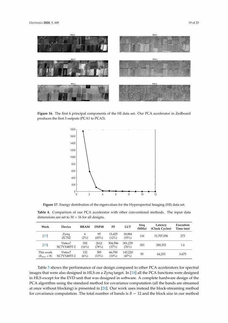
The PCA output images generated by the FPGA are visually the same as the MATLAB output.Figure 16 represents the first six outputs of PCA applied to the hyperspectral images data set. The FPGAproduces the first 3 principal components that are indicated in the figure as PCA1 to PCA3. As shownin the energy distribution in Figure 17, the first 3 principal components contain almost the entireenergy of the input data. The first 3 PCs in Figure 16 correspond to these 3 components. It is evidentfrom Figure 16 that the PCs after the third component do not contain enough information in contrastwith the first 3 PCs.
The flexibility of our PCA accelerator allows us to compare it with other state-of-the-art referencespresenting PCA acceleration with different dimensions and target devices. Table 4 represents theresource usage, frequency and execution time for our FPGA design compared with two otherreferences [15,17]. The input data for all of the references contain 30 rows (pixels) and 16 columns(bands in our design). The first reference uses an HLS approach to design its PCA accelerator ona Zynq FPGA, and the second one uses a manual RTL design in VHDL on a Virtex7 FPGA target.Our HLS design on the same Virtex7 FPGA uses fewer resources as indicated in Table 4. Although theclock frequency of our design is not as high as the previous methods, the total execution time for ourdesign is reduced by a factor 2.3x compared to the same FPGA target.
Electronics 2020, 9, 449 19 of 23
Figure 16. The first 6 principal components of the HI data set. Our PCA accelerator in Zedboardproduces the first 3 outputs (PCA1 to PCA3).
Figure 17. Energy distribution of the eigenvalues for the Hyperspectral Imaging (HI) data set.
Table 4. Comparison of our PCA accelerator with other conventional methods. The input datadimensions are set to 30× 16 for all designs.
Work Device BRAM DSP48 FF LUT freq Latency Execution(MHz) (Clock Cycles) Time (ms)
[17] Zynq 6 95 13,425 18,884 116 31,707,056 273ZC702 (2%) (43%) (12%) (35%)
[15] Virtex7 350 2612 304,596 301,235 183 289,352 1.6XC7VX485T-2 (16%) (78%) (37%) (76%)
This work Virtex7 132 385 66,790 145,220 95 64,253 0.675(Bmax = 8) XC7VX485T-2 (6%) (13%) (10%) (47%)
Table 5 shows the performance of our design compared to other PCA accelerators for spectralimages that were also designed in HLS on a Zynq target. In [18] all the PCA functions were designedin HLS except for the EVD unit that was designed in software. A complete hardware design of thePCA algorithm using the standard method for covariance computation (all the bands are streamedat once without blocking) is presented in [20]. Our work uses instead the block-streaming methodfor covariance computation. The total number of bands is B = 12 and the block size in our method

Electronics 2020, 9, 449 20 of 23
is Bmax = 3. The data representation is floating-point in all of the methods compared in Table 5.As shown in the Table, in our design the DSP and BRAM usage is higher and the FF and LUT usage islower. Despite the reduction in clock frequency, the total execution time of our design is the minimum(0.44 s) among the three accelerators.
Table 5. Comparison of the proposed PCA hardware design with other High Level Synthesis(HLS)-based accelerators. The dimensions of a spectral image data set (640× 480× 12) is selected forall of the designs.
Work Execution Time (s) BRAM (%) DSP48 (%) FF (%) LUT (%) freq (MHz)
[18] (PCA-SVD) 1.1 12 19 38 73 -[20] 0.83 9 32 51 94 100
Ours (Bmax = 3) 0.44 27 53 32 90 90
Finally, our FPGA design is compared with a GPU and MPPA implementation of the PCAalgorithm [16] for different data dimensions as shown in Table 6. In our design, the target device is theVirtex7 FPGA and the block size is set to Bmax = 10 as the numbers of bands are multiples of 10. For thesmaller number of pixels (100× 100), our FPGA design outperforms the other two implementations inGPU and MPPA in terms of execution time. For the larger number of pixels, the execution time forour design increases linearly and becomes more than the other designs. It has to be noted, however,that the typical power consumption in MPPAs and GPUs is significantly more than in FPGAs. In theradar chart in Figure 18, four important factors when selecting a hardware platform are considered andtheir mutual impact is analyzed. These factors are power consumption, latency per pixel, number ofbands (input size) and energy. The axes are normalized to the range 0 to 1 and the scale is logarithmicfor better visualization.
Figure 18. Comparison of different hardware platforms between latency per pixel, power consumption,input size (bands) and energy.
Table 6. Execution time (ms) for the PCA implementation on GPU, Massively Parallel Processing Array(MPPA), and FPGA (our work). The first two designs on GPU and MPPA are from [16].
Dimensions MPPA GPU Ours (FPGA), Bmax = 10
100× 100× 50 140.4 69.28 40.47300× 300× 20 47.2 70.87 62.37300× 300× 30 80.1 70.22 121.9300× 300× 50 170.7 75.74 268.11

Electronics 2020, 9, 449 21 of 23
As shown in Figure 18, for a small number of bands, a Zynq FPGA has a power consumption ofonly 2.37 W with a small latency. For larger bands, although GPUs and MPPAs have smaller latencythan FPGAs, they consume much more power (especially GPUs). By taking into account the energyconsumption that is smaller for FPGAs, one has to select the best hardware based on their needs anduse case. Using an FPGA for the PCA accelerator results in a power efficient hardware that can beused for large input sizes without a significant increase in the total latency.
6. Conclusions
In this paper, we proposed a new hardware accelerator for the PCA algorithm on FPGA byintroducing a new block-streaming method for computing the internal covariance matrix. By dividingthe input data into several blocks of fixed size and reading each block in a specific order, there is noneed to stream the entire data at once, which is one of the main problems of resource overuse in thedesign of PCA accelerators in FPGAs. The proposed PCA accelerator is developed in Vivado HLStool and several hardware optimization techniques are applied to the same design in HLS to improvethe design efficiency. A fixed-point version of our PCA design is also presented, which reduces thePCA latency compared to the floating-point version. Different data dimensions and FPGA targets areconsidered for hardware evaluation, and a hyperspectral image data set is used to assess the proposedPCA accelerator implemented on Zedboard.
Compared to a similar RTL-based FPGA implementation of PCA using VHDL, our HLSdesign has a 2.3× speedup in execution time, as well as a significant reduction of the resourceconsumption. Considering other HLS-based approaches, our design has a maximum of 2.5× speedup.The performance of the proposed FPGA design is compared with similar GPU and MPPAimplementations and, according to the results, the execution time changes with data dimensions.For a small number of pixels our FPGA design outperforms GPU and MPPA designs. For a largenumber of pixels the FPGA implementation remains the most power-efficient one.
Author Contributions: All authors contributed substantially to the paper: conceptualization, M.A.M. and M.R.C.;methodology, M.A.M. and M.R.C.; software, M.A.M.; hardware, M.A.M.; validation, M.A.M. and M.R.C.;writing—original draft preparation, M.A.M.; writing—review and editing, M.R.C.; supervision, M.R.C.;project administration, M.R.C.; funding acquisition, M.R.C. All authors have read and agreed to the publishedversion of the manuscript.
Funding: This work was supported by the EMERALD project funded by the European Union’s Horizon 2020research and innovation programme under the Marie Skłodowska-Curie grant agreement No. 764479.
Conflicts of Interest: The authors declare no conflict of interest. The funders had no role in the design of thestudy; in the collection, analyses, or interpretation of data; in the writing of the manuscript, or in the decision topublish the results.
Abbreviations
The following abbreviations are used in this manuscript:
PCA Principal Component AnalysisPC Principal ComponentMI Microwave ImagingHI Hyperspectral ImagingHLS High Level SynthesisHDL Hardware Description LanguageFPGA Field Programmable Gate ArrayEVD Eigenvalue DecompositionSVD Singular Value DecompositionMPPA Massively Parallel Processing ArrayCov CovariancePU Projection UnitPS Processing SystemPL Parallel LogicSoC System on Chip

Electronics 2020, 9, 449 22 of 23
References
1. Davis, S.K.; Van Veen, B.D.; Hagness, S.C.; Kelcz, F. Breast Tumor Characterization Based on UltrawidebandMicrowave Backscatter. IEEE Trans. Biomed. Eng. 2008, 55, 237–246. [CrossRef] [CrossRef] [PubMed]
2. Ricci, E.; Di Domenico, S.; Cianca, E.; Rossi, T.; Diomedi, M. PCA-based Artifact Removal Algorithm forStroke Detection using UWB Radar Imaging. Med. Biol. Eng. Comput. 2017, 55, 909–921. [CrossRef][CrossRef] [PubMed]
3. Oliveira, B.; Glavin, M.; Jones, E.; O’Halloran, M.; Conceição, R. Avoiding unnecessary breast biopsies:Clinically-informed 3D breast tumour models for microwave imaging applications. In Proceedings ofthe IEEE Antennas and Propagation Society International Symposium (APSURSI), Memphis, TN, USA,6–11 July 2014; pp. 1143–1144. [CrossRef]
4. Gerazov, B.; Conceicao, R.C. Deep learning for tumour classification in homogeneous breast tissue inmedical microwave imaging. In Proceedings of the IEEE EUROCON 17th International Conference on SmartTechnologies, Ohrid, Macedonia, 6–8 July 2017; pp. 564–569. [CrossRef]
5. Torun, M.U.; Yilmaz, O.; Akansu, A.N. FPGA, GPU, and CPU implementations of Jacobi algorithm foreigenanalysis. J. Parallel. Distrib. Comput. 2016. [CrossRef] [CrossRef]
6. Kasap, S.; Redif, S. Novel Field-Programmable Gate Array Architecture for Computing the EigenvalueDecomposition of Para-Hermitian Polynomial Matrices. IEEE Trans. VLSI Syst. 2014, 22, 522–536. [CrossRef][CrossRef]
7. Wang, X.; Zambreno, J. An FPGA Implementation of the Hestenes-Jacobi Algorithm for Singular ValueDecomposition. In Proceedings of the IEEE International Parallel & Distributed Processing SymposiumWorkshops, Phoenix, AZ, USA, 19–23 May 2014; pp. 220–227. [CrossRef]
8. Shuiping, Z.; Xin, T.; Chengyi, X.; Jinwen, T.; Delie, M. Fast implementation for the Singular Value andEigenvalue Decomposition based on FPGA. Chin. J. Electron. 2017, 26, 132–136. [CrossRef]
9. Ma, Y.; Wang, D. Accelerating SVD computation on FPGAs for DSP systems. In Proceedings of the IEEE 13thInternational Conference on Signal Processing (ICSP), Chengdu, China, 6–10 November 2016; pp. 487–490.[CrossRef]
10. Chen, Y.; Zhan, C.; Jheng, T.; Wu, A. Reconfigurable adaptive Singular Value Decomposition engine designfor high-throughput MIMO-OFDM systems. IEEE Trans. VLSI Syst. 2013, 21, 747–760. [CrossRef] [CrossRef]
11. Athi, M.V.; Zekavat, S.R.; Struthers, A.A. Real-time signal processing of massive sensor arrays via a parallelfast converging SVD algorithm: Latency, throughput, and resource analysis. IEEE Sens. J. 2016, 16, 2519–2526.[CrossRef] [CrossRef]
12. Perera, D.G.; Li, K.F. Embedded Hardware Solution for Principal Component Analysis. In Proceedings of theIEEE Pacific Rim Conference on Communications, Computers and Signal Processing, Victoria, BC, Canada,23–26 August 2011; pp. 730–735. [CrossRef]
13. Fernandez, D.; Gonzalez, C.; Mozos, D.; Lopez, S. FPGA implementation of the principal component analysisalgorithm for dimensionality reduction of hyperspectral images. J. Real Time Image Process. 2019, 16, 1–12.[CrossRef] [CrossRef]
14. Das, A.; Nguyen, D.; Zambreno, J.; Memik, G.; Choudhary, A. An FPGA-based network intrusion detectionarchitecture. IEEE Trans. Inf. Forensics Secur. 2008, 3, 118–132. [CrossRef] [CrossRef]
15. Korat, U.A.; Alimohammad, A. A reconfigurable hardware architecture for Principal Component Analysis.Circ. Syst. Signal Process. 2019, 38, 2097–2113. [CrossRef] [CrossRef]
16. Martel, E.; Lazcano, R.; López, J.; Madroñal, D.; Salvador, R.; López, S.; Juarez, E.; Guerra, R.; Sanz, C.;Sarmiento, R. Implementation of the Principal Component Analysis onto High-Performance ComputerFacilities for Hyperspectral Dimensionality Reduction: Results and Comparisons. Remote Sens. 2018, 10, 864.[CrossRef] [CrossRef]
17. Ali, A.A.S.; Amira, A.; Bensaali, F.; Benammar, M. Hardware PCA for gas identification systems using highLevel Synthesis on the Zynq SoC. In Proceedings of the IEEE 20th International Conference on Electronics,Circuits, and Systems (ICECS), Abu Dhabi, United Arab Emirates, 8–11 December 2013; pp. 707–710.[CrossRef]

Electronics 2020, 9, 449 23 of 23
18. Schellhorn, M.; Notni, G. Optimization of a Principal Component Analysis Implementation onField-Programmable Gate Arrays (FPGA) for Analysis of Spectral Images. In Proceedings of the DigitalImage Computing: Techniques and Applications (DICTA), Canberra, Australia, 10–13 December 2018;pp. 1–6. [CrossRef]
19. Mansoori, M.A.; Casu, M.R. Efficient FPGA Implementation of PCA Algorithm for Large Data using HighLevel Synthesis. In Proceedings of the 15th Conference on Ph.D Research in Microelectronics and Electronics(PRIME), Lausanne, Switzerland, 15–18 July 2019; pp. 65–68. [CrossRef]
20. Mansoori, M.A.; Casu, M.R. HLS-Based Flexible Hardware Accelerator for PCA Algorithm on a Low-CostZYNQ SoC. In Proceedings of the IEEE Nordic Circuits and Systems Conference (NORCAS): NORCHIPand International Symposium of System-on-Chip (SoC), Helsinki, Finland, 29–30 October 2019; pp. 1–7.[CrossRef]
21. Manolakis, D.; Shaw, G. Detection Algorithms for Hyperspectral Imaging Applications. IEEE Signal Process.Mag. 2002, 19, 29–43. [CrossRef] [CrossRef]
22. Demmel, J.; Veselic, K. Jacobi’s method is more accurate than QR. SIAM J. Matrix Anal. Appl. 1992,13, 1204–1245. [CrossRef] [CrossRef]
23. Beilina, L.; Karchevskii, E.; Karchevskii, M. Numerical Linear Algebra: Theory and Applications, 1st ed.; SpringerInternational Publishing: Cham, Switzerland, 2017. [CrossRef]
c© 2020 by the authors. Licensee MDPI, Basel, Switzerland. This article is an open accessarticle distributed under the terms and conditions of the Creative Commons Attribution(CC BY) license (http://creativecommons.org/licenses/by/4.0/).