
High-Frequency Clock Distribution Methods in Digital ... · High-Frequency Clock Distribution...
7
High-Frequency Clock Distribution Methods in Digital Integrated Circuits Sajjad Moazeni Electrical Engineering and Computer Sciences University of California at Berkeley Technical Report No. UCB/EECS-2017-116 http://www2.eecs.berkeley.edu/Pubs/TechRpts/2017/EECS-2017-116.html June 6, 2017
Transcript of High-Frequency Clock Distribution Methods in Digital ... · High-Frequency Clock Distribution...

High-Frequency Clock Distribution Methods in DigitalIntegrated Circuits
Sajjad Moazeni
Electrical Engineering and Computer SciencesUniversity of California at Berkeley
Technical Report No. UCB/EECS-2017-116http://www2.eecs.berkeley.edu/Pubs/TechRpts/2017/EECS-2017-116.html
June 6, 2017

Copyright © 2017, by the author(s).All rights reserved.
Permission to make digital or hard copies of all or part of this work forpersonal or classroom use is granted without fee provided that copies arenot made or distributed for profit or commercial advantage and that copiesbear this notice and the full citation on the first page. To copy otherwise, torepublish, to post on servers or to redistribute to lists, requires priorspecific permission.
Acknowledgement
The author would like to thank Prof. A. Niknejad of the University ofCalifornia, Berkeley for his assistance.

1
Abstract—This paper provides a comparative study of the
proposed global clock distribution methods for high-speed digital integrated circuits. Both non-networked and distributed schemes such as travelling and standing wave clock distributions have been reviewed. Performance metrics are described and qualitatively discussed and non-networked approaches were simulated in a low-power 65nm CMOS process.
Index Terms—Clock Distribution, CML Chain, CDW, LC-
resonance, Distributed Clock Networks.
I. INTRODUCTION he rapid trend of computation speed requires high-performance processors and high data-rate
communications (multi-Gbps) for wire-line and optical interconnects at inter and intra chip levels in high performance computing (HPC) and large scale data-centers. Despite the exponential increase in the number of transistors per die, processors’ clock frequency has been barely changed for during the last 10 years and this imposed direct computational bottlenecks [1]. The major reason is that distributing a high-speed clock over a large area of a chip in an energy-efficient way is extremely challenging due to the parasitic capacitance of wirings and device junctions. Traditional clock networks used inverter and buffer chains, which are not energy-efficient at the multi-GHz clock rate since the charging/discharging power consumption of a wire is 𝐶!𝑉!!! 𝑓, which cannot be improved by the Dennard’s scaling down process; 𝐶! remains almost constant for a fixed length wire, 𝑉!! does not scale down and consequently 𝑓 is still limited by the power budget. In addition, signal integrity issues caused by the buffers limit the performance of this approach. To alleviate these problems, multiple alternative methods have been proposed to reduce the capacitance load, using transmission lines instead of the wires, and also distributing the whole clock generators over the chip. In this paper, we studied these different methods used for the clock distribution: buffer chain, current mode logic (CML) clocking, capacitively driven wires (CDW), LC-resonance, and travelling and standing wave schemes using transmission lines. First, we define some of the most important metrics to assess these schemes in the next section. Sections III to VII are
S. Moazeni is with the University of California, Berkeley, CA 94720 USA (e-mail: [email protected]).
dedicated to describe each approach separately, and finally we compare the non-networked methods in Section VIII and conclude the paper in Section IX.
II. CLOCK DISTRIBUTION NETWORK METRICS
A. Power Power consumption is the most critical metric for a clock
distribution network. In most of the high-performance processors, the clock network dissipates more than 30% of the total power. There are mainly 3 methods to manage the power: reduce the clock voltage swing, reduce the effective load capacitance, and use transmission lines. We will discuss the energy-efficiency of each method in the following sections.
B. Jitter Another major consideration is the timing noise and
systematic offsets, known as the clock jitter, caused by the clock source and network. The jitter can be affected by the buffers’ noise, supply’s injected noise, phase mismatch, etc. The tolerable jitter depends on the application and the blocks receiving the clock signal. For instance, if the clock is driving an ADC or a high-speed wire-line transceiver, then the jitter specs directly sets the system performance.
C. Latency/Skew Although the clock edge rates should remain properly fast at
each leaf of the clock distribution tree, each node may see a different delay (or phase) of the clock. The definition of clock skew is the time difference between two clock signals at the half of their voltage swing. At the global clock network level, the goal is mostly to synchronize the clocks at the leaves and each block can tune its proper clock phase via a phase interpolator or delay lines. In another words, skew should be constant for all the clock users on the chip. The absolute skew value might be also a design specified parameter in some applications as well.
D. Area/Cross-section The wiring for clock networks is mostly done at the upper
metal levels due to their low resistance. Same layers are considered for power distribution and implementing inductors for the same reason. Thus, not only we prefer compact clock wiring to accommodate more high-speed transceivers for high bandwidth applications such as switch system-on-chips (SOC), but also it is important to minimize the clock network area to have more room for power grids. This metric restricts the usage of transmission lines for clocking in these chips since they are relatively wider than the normal wires. For
High-Frequency Clock Distribution Methods in Digital Integrated Circuits
Sajjad Moazeni, IEEE Student Member
T

2
Fig. 2. CDW method simulation results in 65nm technology (Red waveforms are the CDW and purple shows the load clock signal using buffer chains)
instance, 32um wide coplanar transmission lines result in the throughput density of 0.25Gb/s/um at 8Gb/s. On the other hand, 1.6um wide thick copper wires with CMOS-based buffers lead to 0.625Gb/s/um areal throughput density at 1Gb/s in an 180𝑛𝑚 technology.
III. BUFFER CHAIN
The most commonly used method of implementing a balanced clock distribution network on a chip is using CMOS-based inverters in a H-tree or grid structure network to balance the skews. The following Elmore delay model can be used to find the optimum sizing of gates and the number and length of segments to minimized the skew:
𝑡! = 𝑁[0.69𝑅!"𝐶!"# + 0.69𝑅!" + 0.38𝑅!𝐿𝑁
𝐶!𝐿𝑁
+ 0.69 𝑅!" +𝑅!𝐿𝑁
𝐶!"]
Where (𝑅! ,𝐶!) are the characteristics of the wire per length (𝐿) and inverters’ specifications are (𝑅!" ,𝐶!",𝐶!"#). Clocking speed is limited by the fan-out of the buffers that limits how fast clock transitions happen. In addition to poor energy-efficiency, the jitter performance in this approach is the poorest compared with the others due to the supply noise (poor PSRR of inverters) and mismatch between buffers. Moreover, process variations and large number of buffers affect the duty-cycle of the clock and consequently this method is not recommended for the large-scale designs.
IV. CML CHAIN CML buffer chain method can be implemented by using CML buffers instead of the CMOS inverters of the previous approach. In doing so, we can reduce the voltage swing to lower power dissipation. Also, the signal is more immune to the noise sources due to the differential signaling. However, the static current drawn from the CML buffers and extra CML to CMOS converters required for recovering the clock swings locally can limit the power efficiency. The number of buffers required for a fixed latency over a fixed length is smaller than the CMOS buffer chains and this can improve the overall energy-efficiency and also the jitter. The jitter and latency performance has been studied in [2], where the simulation on a 5mm wire using 200mV swing CML buffers (𝑅 = 200 𝑜ℎ𝑚, 𝐼 = 1𝑚𝐴,𝑊/𝐿 = 20𝑢/0.1𝑢) lead to the latency of 182ps and the jitter of 0.5ps by setting the optimal number of buffers and wire lengths.
V. CAPACITIVELY DRIVEN WIRES (CDW) In this method, we reduce the load and wiring capacitance
driven by the buffers by simply using a coupling capacitor in series with the load (shown in Fig. 1). The smaller load capacitance improves the delay, energy-efficiency in the price of smaller voltage swing. Similar to the previous approach, we need to recover the swing to the full rail-to-rail swing for each block locally. Also, the clock signals are now more sensitive to cross talk and coupling to other signals. This issue can be
addressed by using the differential signaling. Another disadvantage is that DC bias of the buffers should be set via auxiliary circuitry.
The authors in [3] have implemented and evaluated this approach in an 180nm technology node, assuming 200mV signal swing. The overall energy-efficiency improvement was 3.8x comparing with full swing buffer chains (excluding local buffers). Throughput density was also improved by 1.7x because of the higher clock rate.
Fig. 1 shows the modeling of a single stage CDW clock buffer. The coupling capacitance will reduce the voltage by 𝐶! /(𝐶! + 𝐶! + 𝐶! + 𝐶!). Elmore delay model time-constant for this example can be written as:
𝜏 = 𝑅!"##$% 𝐶!"# + 𝐶! + 𝑅![(𝐶!! +𝐶!2)|| 𝐶! +
𝐶!2
]
= 𝑅!"##$% 𝐶!! + 𝐶! + 𝑅!𝐶!/4
The results for a single stage buffer in 65nm process are shown in Fig. 2 and compared against the conventional approach with no coupling capacitor. Here, we assumed 200mV voltage swing. The wiring load is a 300um long and 4um wide top copper metal layer with 4x thickness. Also, 𝐶! = 𝐶! = 20𝑓𝐹 and the buffer size was set to 300um. Series capacitor clearly improved the rising/falling time and delay.
Fig. 1. Modeling of a single ended CDW clock buffer [3].

3
Fig. 3. LC-resonance scheme simulation results in 65nm (Red curve is the LC-resonated clock versus the original CML clock shown in green)
Fig. 4. Basic travelling wave oscillator concept [4].
Fig. 5. Basic travelling wave oscillators from [4].
However, the clock signal’s swing over the load is only 125mV that needs to get amplified and recovered for digital circuits operating at the full swing signal.
VI. LC- RESONANCE Another scheme to reduce the effective load capacitance
seen by the clock buffers is to use LC-resonance. By using an inductor, we can cancel out some portion of 𝐶! at the clock frequency and improve the clock rate, energy-efficiency, and the delay. Main advantage of this approach over the previous two methods is that the propagated clock signal can keep its large swing through the clock path and there’s no need to recover the swing. In addition, LC-resonance helps to reduce the jitter by filtering out the phase noise out of the clock frequency band. Fig. 3 shows the simulation result of this method in 65nm technology node. In this simulation, the wiring load is still assumed to be a 300um/4um thick metal layer with 𝐶! =20𝑓𝐹, 𝐿 = 12𝑛𝐻 and we used a CML buffer cell (𝑅 =100 𝑜ℎ𝑚, 𝐼 = 1 𝑚𝐴). LC-resonance enhanced the clock edge rates, however the overshoots after adding the inductor should be taken into account for reliability issues. Implementing this method in the high-performance processors is challenging since adding inductors normally require some cuts in the power grid as they are both on the same metal layers.
VII. DISTRIBUTED CLOCK NETWORKS The power consumptions of clock networks studied so far,
could be derived from 𝐶𝑉!𝑓, where 𝐶 is the total capacitance of the wiring and loads. As the frequency increases, the power linearly increases as well. We can use the transmission lines (TL) instead of narrow wires to propagate the clock over the chip; the power can be calculated from driving a 𝑍! load power in addition to the TL losses (𝑅𝐼! where R is the loss). Generally there are two approaches for implementing this:
A. Travelling wave, B. Standing wave. In the travelling wave approach, a closed loop path
(differential or single) with inverting stages is used in order to generate the oscillating signal over the chip. These clock sources are called rotary travelling wave oscillators (RTWO) and the clock phase at loads depend on the position of loading nodes in the loop. Transmission lines can be implemented in the top thick metal layers with low sheet resistances. Since
they are passive elements, they are less sensitive to process variation and do not add up to the jitter noise. In some applications of the distributed networks, designers used PLL or DLL blocks to control the skew and jitter of the clock. In the following subsections, we briefly discuss both of the proposed architectures.
A. Travelling Wave Clock Distribution In [4] authors used a network of coupled RTWOs to make a global clock network. The basic oscillator element (Fig. 4) is a transmission line connected to an impedance-matched inverter output, and the end of the line is connected to a high-impedance input of an inverter.
The RTWO operate as follows; Once the inverter is powered, the output voltage, 𝑉!! /2, propagates through the TL and since loading is ideally high-impedance Γ = 1, which leads to doubling the voltage at the inverter input and consequently, switching the inverter output. Now, the zero voltage propagates with the time delay of 𝑇! and creates once oscillation cycle. So the clock signal frequency is 1/2𝑇!, where 𝑇! = 𝑙/𝑣 and 𝑙 and 𝑣 are length and phase velocity in the TL, respectively. However, non-idealities can cause certain issues: 1. Transmission lines are lossy, 2. Impedances are not perfectly matched and open, 3. The delay of inverter is not zero and should be taken into account. In the realistic case the frequency of oscillation will be different because of parasites. If we distribute the parasitic capacitances along the TL length (𝑙), more accurate oscillation frequency can be derived from:
𝑓 =1
2𝑙 𝐿(𝐶 + (𝐶! + 𝐶!)/𝑙)
Power consumption can be estimated from the total short circuit and switching power dissipated by the inverter and the impedance and series-resistance loss of the TL. By coupling multiple of these distributed oscillators, we can take the advantage of phase averaging and reduce skew and jitter. Fig. 5 illustrates two of the proposed coupling architectures from [4]. It is claimed that the first method reduces the jitter because of phase averaging and the second one can achieve very low skew.

4
Fig. 7. Standing wave oscillators with 3 cross-coupled pairs [6].
Fig. 8. Clock buffers used in [6].
Fig. 6. Network of coupled RTWOs Architecture [5].
Simulation and measurement results of this method in
TSMC 0.18um technology using the transmission line of (𝑙 = 5𝑚𝑚 𝑅 = 50𝑜ℎ𝑚/𝑐𝑚 𝐿 = 4𝑛𝐻/𝑐𝑚 𝐶 = 1.2 𝑝𝑓/𝑐𝑚) at 10GHz clock rate shows 5.48mW power efficiency, which is 30% less than the estimated power of the buffer chains (𝐶𝑉!𝑓). In [5] authors used the differential signaling and used cross-coupled inverter buffers in a fashion similar to a Mobius strip (Fig. 6). The theory is the same as the single line RTWOs [4], however the high-speed clock signals in this method show less cross talk with other sensitive wires on the chip since the magnetic field and return path is confined. Also the jitter is improved due to the differential signaling.
B. Standing Wave Clock Distribution Coupled network of the standing wave oscillators (SWO) (Fig. 7) can be the alternative for RTWO based distributions [6]. Here, authors used a section of 𝜆/2 long transmission line with shorted endings and use negative resistance active cells (cross-coupled transistor pairs) to compensate the loss and eventually create a distributed clock generator over a large area of a die.
By distributing the transconductance of N cross-coupled pairs over the TL length (L), we can derive the propagation constant as follows:
𝛾 = (𝑅 + 𝑗𝑤𝐿)(−𝑁𝑔!𝑙
+ 𝑗𝑤(𝐶 +𝑁𝑐!𝑙))
Where 𝑅𝐿𝐶 is the characteristic of the TL, 𝑔! is the transconductance of each cell, and 𝑐! is the parasite capacitance of each negative-gm cell. So each cell should be designed that 𝑔!/𝑐! is maximum.
To couple these SWOs they chose to couple them from 15%-20% of length from each end. Systematic skews can be avoided by drawing the layout symmetrically. Considering the Phase averaging property of coupled oscillators grid, the jitter and skew in the global network is lower than the conventional methods. Buffers shown in Fig. 8 have been used locally to convert the low swing differential clock signal to the full swing CMOS level. The first stage is a differential amplifier with LP loading to reduce jitter and harmonics. The second stage is used to transform sine wave to full square form by using the cross-coupled latches. The shunt resistance is used to avoid the process, frequency, and temperature variations on the duty cycle.
This approach has been also proposed for clock distribution and synchronization of the wafer scale systems [7]. For their application, a large-scale phased array radio over a wafer, the power and jitter specs are very stringent. So they added a distributed PLL grid network to a coupled network of SWOs to alleviate the jitter and skew issues.
The SWO is implemented similar to [6] by shorting the twos sides of a transmission lines and adding the –𝐺! stages to compensate the line losses. Because of the injection locking between the oscillators, the steady state skew can be derived by setting 𝑑𝜃/𝑑𝑡 = 0 in:
𝑑𝜃!𝑑𝑡
= 𝜔! +𝐾𝑁
sin (𝜃! − 𝜃!)!
!!!
Δ𝑡!"#$ =𝑇2𝜋
sin!!(∆𝜔𝐾)
The optimum coupling point of the SWO unit cells can be
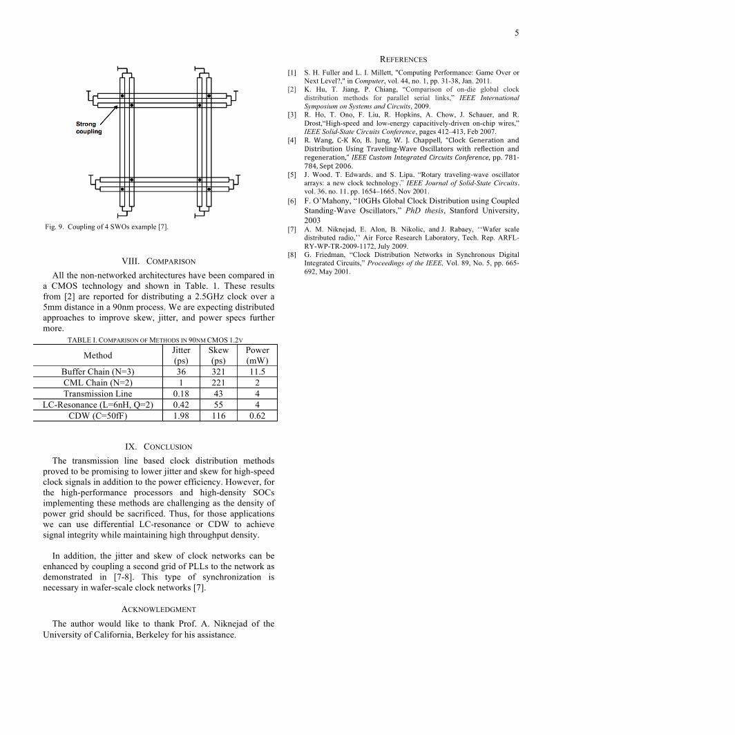
different for optimizing the skew or jitter. Although, from the jitter perspective buffers should be coupled to the point where the signal strength is maximum, authors of [7] proposed a grid shown in Fig. 9 to minimize the skew between the clock leaves.
5
Fig. 9. Coupling of 4 SWOs example [7].
VIII. COMPARISON All the non-networked architectures have been compared in
a CMOS technology and shown in Table. 1. These results from [2] are reported for distributing a 2.5GHz clock over a 5mm distance in a 90nm process. We are expecting distributed approaches to improve skew, jitter, and power specs further more.
IX. CONCLUSION The transmission line based clock distribution methods
proved to be promising to lower jitter and skew for high-speed clock signals in addition to the power efficiency. However, for the high-performance processors and high-density SOCs implementing these methods are challenging as the density of power grid should be sacrificed. Thus, for those applications we can use differential LC-resonance or CDW to achieve signal integrity while maintaining high throughput density.
In addition, the jitter and skew of clock networks can be
enhanced by coupling a second grid of PLLs to the network as demonstrated in [7-8]. This type of synchronization is necessary in wafer-scale clock networks [7].
ACKNOWLEDGMENT The author would like to thank Prof. A. Niknejad of the
University of California, Berkeley for his assistance.
REFERENCES [1] S. H. Fuller and L. I. Millett, "Computing Performance: Game Over or
Next Level?," in Computer, vol. 44, no. 1, pp. 31-38, Jan. 2011. [2] K. Hu, T. Jiang, P. Chiang, “Comparison of on-die global clock
distribution methods for parallel serial links,” IEEE International Symposium on Systems and Circuits, 2009.
[3] R. Ho, T. Ono, F. Liu, R. Hopkins, A. Chow, J. Schauer, and R. Drost,“High-speed and low-energy capacitively-driven on-chip wires,” IEEE Solid-State Circuits Conference, pages 412–413, Feb 2007.
[4] R. Wang, C-K Ko, B. Jung, W. J. Chappell, “Clock Generation andDistribution Using Traveling-Wave Oscillators with reflection andregeneration,” IEEECustomIntegratedCircuitsConference,pp.781-784,Sept2006.
[5] J. Wood, T. Edwards, and S. Lipa, “Rotary traveling-wave oscillator arrays: a new clock technology,” IEEE Journal of Solid-State Circuits, vol. 36, no. 11, pp. 1654–1665, Nov 2001.
[6] F. O’Mahony, “10GHs Global Clock Distribution using Coupled Standing-Wave Oscillators,” PhD thesis, Stanford University, 2003
[7] A. M. Niknejad, E. Alon, B. Nikolic, and J. Rabaey, ‘‘Wafer scale distributed radio,’’ Air Force Research Laboratory, Tech. Rep. ARFL-RY-WP-TR-2009-1172, July 2009.
[8] G. Friedman, “Clock Distribution Networks in Synchronous Digital Integrated Circuits,” Proceedings of the IEEE, Vol. 89, No. 5, pp. 665-692, May 2001.
TABLE I. COMPARISON OF METHODS IN 90NM CMOS 1.2V
Method Jitter (ps)
Skew (ps)
Power (mW)
Buffer Chain (N=3) 36 321 11.5 CML Chain (N=2) 1 221 2 Transmission Line 0.18 43 4
LC-Resonance (L=6nH, Q=2) 0.42 55 4 CDW (C=50fF) 1.98 116 0.62


