High Efficiency Low-Side Controller with True … · important notice
37
Copyright © 2016, Texas Instruments Incorporated Product Folder Sample & Buy Technical Documents Tools & Software Support & Community An IMPORTANT NOTICE at the end of this data sheet addresses availability, warranty, changes, use in safety-critical applications, intellectual property matters and other important disclaimers. PRODUCTION DATA. LM3017 SNOSC66D – MARCH 2012 – REVISED SEPTEMBER 2016 LM3017 High Efficiency Low-Side Controller With True Shutdown 1 1 Features 1• Fully Compliant to Thunderbolt™ Technology Specifications • True Shutdown for Short-Circuit Protection • Input Side Current Limit • Single Enable Pin With Three Modes of Operation: Boost, Pass-Through, or Shutdown • Built-in Charge Pump for High-Side NFET Disconnect Switch • 1-A Push-Pull Driver for Low-Side NFET • Peak Current Mode Control • Simple Slope Compensation • Protection Features: Thermal Shutdown, Cycle- by-Cycle Current Limit, Short-Circuit Protection, Output Overvoltage Protection, and Latch-Off • Internal Soft Start • Input Voltage Range: 5 V to 18 V • 600-kHz Fixed Frequency Operation • ±1% Reference Voltage Accuracy Over Temperature • Low Shutdown Current (< 1 μA), 40 nA Typical • 2.4 mm × 2.7 mm × 0.8 mm, 10-Pin WQFN Package 2 Applications • Thunderbolt™ Technology Host Ports • Notebook and Desktop Computers, Tablets, and Other Portable Consumer Electronics • Hard Disc Drives, Solid-State Drives • Offline Power Supplies • Set-Top Boxes 3 Description The LM3017 device is a versatile low-side NFET controller incorporating true shutdown and input side current limiting. The LM3017 is designed for simple implementation of boost conversions in Thunderbolt™ Technology. The LM3017 can also be configured for flyback or SEPIC designs. The input voltage range of 5 V to 18 V accommodates a two- or three-cell lithium ion battery or a 12-V rail. The enable pin accepts a single input to drive three different modes of operation: boost, pass-through, or shutdown mode. The LM3017 draws very low current in shutdown mode, typically 40 nA from the input supply. The LM3017 provides an adjustable output to drive the Power Load Switch or MUX for the host Thunderbolt™ port. The ability to drive an external high-side NMOS provides for true isolation of the load from the input. Current limiting on the input ensures that inrush and short-circuit currents are always under control. The LM3017 incorporates built-in thermal shutdown, cycle-by-cycle current limit, short-circuit protection, output overvoltage protection, and soft start. It is available in a 10-pin WQFN package. Device Information (1) PART NUMBER PACKAGE BODY SIZE (NOM) LM3017 WQFN (10) 2.40 mm × 2.70 mm (1) For all available packages, see the orderable addendum at the end of the data sheet. Typical Application Circuit
Transcript of High Efficiency Low-Side Controller with True … · important notice

Copyright © 2016, Texas Instruments Incorporated
Product
Folder
Sample &Buy
Technical
Documents
Tools &
Software
Support &Community
An IMPORTANT NOTICE at the end of this data sheet addresses availability, warranty, changes, use in safety-critical applications,intellectual property matters and other important disclaimers. PRODUCTION DATA.
LM3017SNOSC66D –MARCH 2012–REVISED SEPTEMBER 2016
LM3017 High Efficiency Low-Side Controller With True Shutdown
1
1 Features1• Fully Compliant to Thunderbolt™ Technology
Specifications• True Shutdown for Short-Circuit Protection• Input Side Current Limit• Single Enable Pin With Three Modes of
Operation: Boost, Pass-Through, or Shutdown• Built-in Charge Pump for High-Side NFET
Disconnect Switch• 1-A Push-Pull Driver for Low-Side NFET• Peak Current Mode Control• Simple Slope Compensation• Protection Features: Thermal Shutdown, Cycle-
by-Cycle Current Limit, Short-Circuit Protection,Output Overvoltage Protection, and Latch-Off
• Internal Soft Start• Input Voltage Range: 5 V to 18 V• 600-kHz Fixed Frequency Operation• ±1% Reference Voltage Accuracy Over
Temperature• Low Shutdown Current (< 1 µA), 40 nA Typical• 2.4 mm × 2.7 mm × 0.8 mm, 10-Pin WQFN
Package
2 Applications• Thunderbolt™ Technology Host Ports• Notebook and Desktop Computers, Tablets, and
Other Portable Consumer Electronics• Hard Disc Drives, Solid-State Drives• Offline Power Supplies• Set-Top Boxes
3 DescriptionThe LM3017 device is a versatile low-side NFETcontroller incorporating true shutdown and input sidecurrent limiting. The LM3017 is designed for simpleimplementation of boost conversions inThunderbolt™ Technology. The LM3017 can also beconfigured for flyback or SEPIC designs. The inputvoltage range of 5 V to 18 V accommodates a two- orthree-cell lithium ion battery or a 12-V rail. The enablepin accepts a single input to drive three differentmodes of operation: boost, pass-through, orshutdown mode. The LM3017 draws very low currentin shutdown mode, typically 40 nA from the inputsupply.
The LM3017 provides an adjustable output to drivethe Power Load Switch or MUX for the hostThunderbolt™ port. The ability to drive an externalhigh-side NMOS provides for true isolation of the loadfrom the input. Current limiting on the input ensuresthat inrush and short-circuit currents are always undercontrol. The LM3017 incorporates built-in thermalshutdown, cycle-by-cycle current limit, short-circuitprotection, output overvoltage protection, and softstart. It is available in a 10-pin WQFN package.
Device Information(1)
PART NUMBER PACKAGE BODY SIZE (NOM)LM3017 WQFN (10) 2.40 mm × 2.70 mm
(1) For all available packages, see the orderable addendum atthe end of the data sheet.
Typical Application Circuit

2
LM3017SNOSC66D –MARCH 2012–REVISED SEPTEMBER 2016 www.ti.com
Product Folder Links: LM3017
Submit Documentation Feedback Copyright © 2012–2016, Texas Instruments Incorporated
Table of Contents1 Features .................................................................. 12 Applications ........................................................... 13 Description ............................................................. 14 Revision History..................................................... 25 Pin Configuration and Functions ......................... 36 Specifications......................................................... 4
6.1 Absolute Maximum Ratings ...................................... 46.2 ESD Ratings.............................................................. 46.3 Recommended Operating Conditions....................... 46.4 Thermal Information .................................................. 46.5 Electrical Characteristics........................................... 56.6 Typical Characteristics .............................................. 7
7 Detailed Description .............................................. 97.1 Overview ................................................................... 97.2 Functional Block Diagram ......................................... 97.3 Feature Description................................................. 107.4 Device Functional Modes........................................ 12
8 Application and Implementation ........................ 148.1 Application Information............................................ 148.2 Typical Application .................................................. 14
9 Power Supply Recommendations ...................... 2810 Layout................................................................... 28
10.1 Layout Guidelines ................................................. 2810.2 Layout Examples................................................... 3010.3 Thermal Considerations ........................................ 30
11 Device and Documentation Support ................. 3111.1 Documentation Support ........................................ 3111.2 Receiving Notification of Documentation Updates 3111.3 Community Resources.......................................... 3111.4 Trademarks ........................................................... 3111.5 Electrostatic Discharge Caution............................ 3111.6 Glossary ................................................................ 31
12 Mechanical, Packaging, and OrderableInformation ........................................................... 31
4 Revision HistoryNOTE: Page numbers for previous revisions may differ from page numbers in the current version.
Changes from Revision C (March 2013) to Revision D Page
• Added ESD Ratings table, Feature Description section, Device Functional Modes, Application and Implementationsection, Power Supply Recommendations section, Layout section, Device and Documentation Support section, andMechanical, Packaging, and Orderable Information section .................................................................................................. 1
• Changed RθJA value in the Thermal Information table From: 36 To: 79.2.............................................................................. 4
Changes from Revision B (November 2012) to Revision C Page
• Added Updated to Rev C as Rev A and B were SVA Confidentials ...................................................................................... 1

30180903
3
LM3017www.ti.com SNOSC66D –MARCH 2012–REVISED SEPTEMBER 2016
Product Folder Links: LM3017
Submit Documentation FeedbackCopyright © 2012–2016, Texas Instruments Incorporated
(1) A = Analog, G = Ground, O = Output, P = Power
5 Pin Configuration and Functions
NKL Package10-Pin WQFN
Top View
Pin FunctionsPIN
TYPE (1) DESCRIPTIONNO. NAME
1 VCC O Driver supply voltage pin: output of internal regulator powering low side NMOS driver. A minimum of0.47 µF must be connected from this pin to PGND for proper operation.
2 DR O Low-side NMOS gate driver output: output gate drive to low side NMOS gate.
3 PGND G Power ground: ground for power section. External power circuit reference. Must be connected toAGND at a single point.
4 VG O High side NMOS gate driver output: output gate drive to high side NMOS gate.
5 EN/MODE A Multi-function input pin: this input provides for chip enable, and mode selection. See DeviceFunctional Modes for details.
6 FB A Feed-back input pin: negative input to error amplifier. Connect to feedback resistor tap to regulateoutput.
7 COMP A Compensation pin: a resistor and capacitor combination connected to this pin provides frequencycompensation for the regulator control loop.
8 AGND G Analog ground: ground for analog control circuitry. Reference point for all stated voltages.9 ISEN A Current sense input: current sense input, with respect to VIN, for all current limit functions.
10 VIN P Power supply input pin: input supply to regulator. See Application and Implementation forrecommendations on bypass capacitors on this pin.

4
LM3017SNOSC66D –MARCH 2012–REVISED SEPTEMBER 2016 www.ti.com
Product Folder Links: LM3017
Submit Documentation Feedback Copyright © 2012–2016, Texas Instruments Incorporated
(1) Stresses beyond those listed under Absolute Maximum Ratings may cause permanent damage to the device. These are stress ratingsonly, which do not imply functional operation of the device at these or any other conditions beyond those indicated under RecommendedOperating Conditions. Exposure to absolute-maximum-rated conditions for extended periods may affect device reliability.
(2) If Military/Aerospace specified devices are required, please contact the Texas Instruments Sales Office/Distributors for availability andspecifications.
6 Specifications
6.1 Absolute Maximum Ratingsover operating free-air temperature range (unless otherwise noted) (1) (2)
MIN MAX UNITVIN to PGND, AGND –0.3 20 VFB, COMP, VCC,DR to PGND, AGND –0.2 6 VEN/MODE –0.2 5.5 VVG –0.3 VIN + 6 VISEN to PGND, AGND VIN – 0.3 VIN VPeak low side driver output current 1 APower dissipation Internally limitedJunction temperature, TJ 150 °CStorage temperature, Tstg –65 150 °C
(1) JEDEC document JEP155 states that 500-V HBM allows safe manufacturing with a standard ESD control process.
6.2 ESD RatingsVALUE UNIT
V(ESD) Electrostatic discharge Human-body model (HBM), per ANSI/ESDA/JEDEC JS-001 (1) ±1500 V
6.3 Recommended Operating Conditionsover operating free-air temperature range (unless otherwise noted)
MIN MAX UNITVIN Supply voltage 5.4 18 VTJ Junction temperature –40 125 °C
(1) For more information about traditional and new thermal metrics, see the Semiconductor and IC Package Thermal Metrics applicationreport.
6.4 Thermal Information
THERMAL METRIC (1)LM3017
UNITNKL (WQFN)10 PINS
RθJA Junction-to-ambient thermal resistance 79.2 °C/WRθJC(top) Junction-to-case (top) thermal resistance 29.8 °C/WRθJB Junction-to-board thermal resistance 21.4 °C/WψJT Junction-to-top characterization parameter 0.6 °C/WψJB Junction-to-board characterization parameter 20.7 °C/WRθJC(bot) Junction-to-case (bottom) thermal resistance — °C/W
5
LM3017www.ti.com SNOSC66D –MARCH 2012–REVISED SEPTEMBER 2016
Product Folder Links: LM3017
Submit Documentation FeedbackCopyright © 2012–2016, Texas Instruments Incorporated
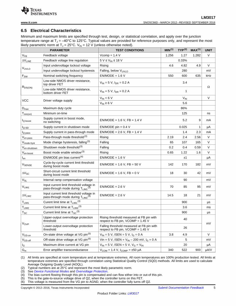
(1) All limits are specified at room temperature and at temperature extremes. All room temperatures are 100% production tested. All limits attemperature extremes are specified through correlation using Statistical Quality Control (SQD) methods. All limits are used to calculateAverage Outgoing Quaity Level (AOQL).
(2) Typical numbers are at 25°C and represent the most likely parametric norm.(3) See Device Functional Modes and Overvoltage Protection.(4) The bias current flowing through this pin is compensated and can flow either into or out-of this pin.(5) This is the gate-to-source voltage drive of Q2, when the controller turns on this FET.(6) This voltage is measured from the VG pin to AGND, when the controller fully turns off Q2.
6.5 Electrical CharacteristicsMinimum and maximum limits are specified through test, design, or statistical correlation, and apply over the junctiontemperature range at TJ = –40°C to 125°C. Typical values are provided for reference purposes only, and represent the mostlikely parametric norm at TJ = 25°C. VIN = 12 V (unless otherwise noted).
PARAMETER TEST CONDITIONS MIN (1) TYP (2) MAX (1) UNITVFB Feedback voltage Vcomp = 1.4 V 1.256 1.27 1.282 VΔVLINE Feedback voltage line regulation 5 V ≤ VIN ≤ 18 V 0.33%
VUVLOInput undervoltage lockout voltage Rising 4.6 4.82 4.9 VInput undervoltage lockout hysteresis Falling, below VUVLO 280 mV
FSW Nominal switching frequency EN/MODE = 1.6 V 550 600 635 kHz
RDS(ON)
Low-side NMOS driver resistance,top driver FET VIN = 5 V, IDR = 0.2 A 3.4
ΩLow-side NMOS driver resistance,bottom driver FET VIN = 5 V, IDR = 0.2 A 1
VCC Driver voltage supplyVIN < 6 V VIN VVIN ≥ 6 V 5.6
Dmax Maximum duty cycle 86%Tmin(on) Minimum on-time 125 ns
IQ-boostSupply current in boost mode,no switching EN/MODE = 1.6 V, FB = 1.4 V 5.2 9 mA
IQ-SD Supply current in shutdown mode EN/MODE pin = 0.4 V 0.025 1 µAIQ-pass Supply current in pass-through mode EN/MODE = 2.6 V, FB = 1.4 V 1.4 2.3 mAVen-pass Pass-through mode threshold (3) Rising 2.19 2.4 2.56 VVmode-hyst Mode change hysteresis, falling (3) Falling 65 107 165 VVen-shutdown Shutdown mode threshold (3) Falling 0.2 0.4 0.59 VVen-boost Boost mode enable window (3) Rising 0.65 1.22 1.6 VIen EN/MODE pin bias current (4) EN/MODE = 1.6 V ±1 µA
VSENSECycle-by-cycle current limit thresholdduring boost mode EN/MODE = 1.6 V, FB = 50 V 142 170 182 mV
ΔVSCShort-circuit current limit thresholdduring boost mode EN/MODE = 1.6 V, FB = 0 V 18 30 42 mV
VSL Internal ramp compensation voltage 90 mV
VLIM1Input current limit threshold voltage inpass-through mode during TLIM1
(3) EN/MODE = 2.6 V 70 85 95 mV
ΔVLIM2Input current limit threshold voltage inpass-through mode during TLIM2
(3) EN/MODE = 2.6 V 14.5 18 21 mV
TLIM1 Curent limit time at TLIM1(3) 900 µs
TLIM2 Current limit time at TLIM2(3) 3.6 ms
TSC Current limit time at TSC(3) 900 µs
VOVP
Upper-output overvoltage protectionthreshold
Rising threshold measured at FB pin withrespect to FB pin, VCOMP = 1.45 V 40
mVLower-output overvoltage protectionthreshold
Falling threshold measured at FB pin withrespect to FB pin, VCOMP = 1.45 V 26
VGS-on On-state drive voltage at VG pin (5) VIN = 5 V, ISEN = 5 V, IG = 0 A 3.8 4.9 VVGS-off Off-state drive voltage at VG pin (6) Vin = 5 V, ISEN = VIN – 200 mV, IG = 0 A 5 mVIG Maximum drive current at VG pin VIN = 5 V, ISEN = 5 V, VG = VIN 20 µAGm Error amplifier transconductance VCOM = 1.4 V, ICOMP = ±50 µA 340 522 900 µA/V

6
LM3017SNOSC66D –MARCH 2012–REVISED SEPTEMBER 2016 www.ti.com
Product Folder Links: LM3017
Submit Documentation Feedback Copyright © 2012–2016, Texas Instruments Incorporated
Electrical Characteristics (continued)Minimum and maximum limits are specified through test, design, or statistical correlation, and apply over the junctiontemperature range at TJ = –40°C to 125°C. Typical values are provided for reference purposes only, and represent the mostlikely parametric norm at TJ = 25°C. VIN = 12 V (unless otherwise noted).
PARAMETER TEST CONDITIONS MIN (1) TYP (2) MAX (1) UNIT
(7) This parameter is calculated from the error amplified Gm and AVOL, and is not tested.
AVOL Error amplifier open-loop voltage gain VCOM = 1.2 V to 1.8 V, ICOMP = 0 A 190 313 450 V/V
ROError amplifier open-loop outputresistance (7) 600 kΩ
IEAO Error amplifier output current swingsSourcing: VCOMP = 1.4 V, VFB = 1.1 V 27 66 115
µASinking: VCOMP = 1.4 V, VFB = 1.4 V 49 68 125
VEAO Error amplifier output voltage limitsUpper: VFB = 0 V, COMP pin floating 2.3
VLower: VFB = 1.4 V 0.82
Tr Drive pin rise time Cload = 3 nF, VDR = 0 V to 3 V 25 nsTf Drive pin fall time Cload = 3 nF, VDR = 3 V to 0 V 25 nsTSD Thermal shutdown threshold 165 °CTSD-hyst Thermal shutdown threshold hysteresis 10 °C

-60 -40 -20 0 20 40 60 80 100
0.5
1.0
1.5
2.0
2.5
3.0
3.5
4.0
4.5
5.0
CU
RR
EN
T L
IMIT
TIM
ING
(m
s)
TEMPERATURE (°C)
TLIM1TLIM2
4 5 6 7 8 9 10 11 12 13 14
2.5
3.0
3.5
4.0
4.5
5.0
5.5
6.0
6.5
PA
SS
FE
T G
AT
E-S
OU
RC
E V
OLT
AG
E (
V)
INPUT VOLTAGE (V)
-40°C27°C90°C
4 6 8 10 12 14 16 183.0
3.2
3.4
3.6
3.8
4.0
SU
PP
LY C
UR
RE
NT
(m
A)
INPUT VOLTAGE (V)
-40°C27°C90°C
-60 -40 -20 0 20 40 60 80 100
110
115
120
125
130
135
140
145
MIN
IMU
M O
N-T
IME
(ns
)
TEMPERATURE (°C)
-60 -40 -20 0 20 40 60 80 100
550
560
570
580
590
600
610
620
630
640
650
FR
EQ
UE
NC
Y (
kHz)
TEMPERATURE (°C)
8V12V
4 6 8 10 12 14 16 18
0.8
1.0
1.2
1.4
1.6
SU
PP
LY C
UR
RE
NT
(m
A)
INPUT VOLTAGE (v)
-40°C27°C90°C
7
LM3017www.ti.com SNOSC66D –MARCH 2012–REVISED SEPTEMBER 2016
Product Folder Links: LM3017
Submit Documentation FeedbackCopyright © 2012–2016, Texas Instruments Incorporated
6.6 Typical CharacteristicsVIN = 12 V, TJ = 25°C, and see Figure 16 (unless otherwise noted).
Figure 1. Switching Frequency vs Temperature Figure 2. Supply Current in Pass-Through Mode (IG-pass)
Figure 3. Supply Current in Boost Mode (IQ-boost) Figure 4. Minimum ON-Time vs Temperature
Figure 5. Current Limit Timing vs Temperature Figure 6. Pass FET Drive Voltage vs Input Voltage (VGS-on)

8 9 10 11 12
-0.25
-0.20
-0.15
-0.10
-0.05
0.00
0.05
0.10
0.15
0.20
0.25
ûV
OU
T(%
)
INPUT VOLTAGE (V)
0.1A output current0.5A output current1A output current
500 mV/Div5V/Div
200 mA/Div
TIME (5 ms/DIV)
EN
IO
VO
0.0 0.1 0.2 0.3 0.4 0.5 0.6 0.7 0.8 0.9 1.0
80
82
84
86
88
90
92
94
96
98
100
EF
FIC
IEN
CY
(%
)
OUTPUT CURRENT (A)
8Vin10Vin12Vin
0.0 0.1 0.2 0.3 0.4 0.5 0.6 0.7 0.8 0.9 1.0
-0.25
-0.20
-0.15
-0.10
-0.05
0.00
0.05
0.10
0.15
0.20
0.25
ûV
OU
T(%
)
OUTPUT CURRENT (A)
8Vin10Vin12Vin
-60 -40 -20 0 20 40 60 80 100
10
15
20
25
30
35
PA
SS
FE
T G
AT
E D
RIV
E C
UR
RE
NT
(�
A)
TEMPERATURE (°C)
VIN = 12V
2 3 4 5 6 7 8 9 10 11 124.8
5.0
5.2
5.4
5.6
5.8
6.0
6.2
VC
C (
V)
INPUT VOLTAGE (V)
-40°C27°C90°C
8
LM3017SNOSC66D –MARCH 2012–REVISED SEPTEMBER 2016 www.ti.com
Product Folder Links: LM3017
Submit Documentation Feedback Copyright © 2012–2016, Texas Instruments Incorporated
Typical Characteristics (continued)VIN = 12 V, TJ = 25°C, and see Figure 16 (unless otherwise noted).
Figure 7. Pass FET Drive Current vs Temperature Figure 8. VCC Voltage vs Input Voltage
VOUT = 15 V
Figure 9. Efficiency Figure 10. Load Regulation
Figure 11. Line Regulation
VIN = 8 V
Figure 12. Start-Up Waveforms

InternalReg
Drive Logic
+
-
�
Internal Slope Compensation
OSC
+
-
PWM
Limit
+-
LimitReferences
+
-E.A.
Current SenseAmp.
1.27VReference
SoftStart
OVP
EN/MODELogic
PassControl
ChargePump
VIN
VCC
DR
PGNDAGNDFB COMPEN/MODE
VG ISEN
Ramp Adjust
+
-
+
200 mV
-
Short-circuitComparator
A
Level Shifter
Copyright © 2016, Texas Instruments Incorporated
9
LM3017www.ti.com SNOSC66D –MARCH 2012–REVISED SEPTEMBER 2016
Product Folder Links: LM3017
Submit Documentation FeedbackCopyright © 2012–2016, Texas Instruments Incorporated
7 Detailed Description
7.1 OverviewThe LM3017 uses a fixed frequency, Pulse Width Modulated (PWM), current mode control architecture. A high-side current sense amplifier provides inductor current information by sensing the voltage drop across RSEN. Thevoltage across this resistor is fed into the ISEN pin. This voltage is then level shifted and fed into the positive inputof the PWM comparator. As with all architectures of this type, a compensation ramp is required to ensure stabilityof the current control loop under all operating conditions. A nominal value of the ramp is provided internally whileadditional ramp can be added through the ISEN pin. The output voltage is sensed through an external feedbackresistor divider network and fed into the error amplifier (EA) negative input (feedback pin, FB). The output of theerror amplifier (COMP pin) is added to the slope compensation ramp and fed into the negative input of the PWMcomparator.
At the start of any switching cycle, the oscillator sets a high signal on the DR pin (gate of the external MOSFET)and the external MOSFET turns on. When the voltage on the positive input of the PWM comparator exceeds thenegative input, the Drive Logic is reset and the external MOSFET turns off.
Under extremely light load or no-load conditions, the energy delivered to the output capacitor when the externalMOSFET is on during the minimum on time is more than what is delivered to the load. An overvoltagecomparator inside the LM3017 prevents the output voltage from rising under these conditions by sensing thefeedback (FB pin) voltage and resetting the RS latch. The latch remains in a reset state until the output decays tothe nominal value. Thus the operating frequency decreases at light loads, resulting in excellent efficiency.
7.2 Functional Block Diagram

10
LM3017SNOSC66D –MARCH 2012–REVISED SEPTEMBER 2016 www.ti.com
Product Folder Links: LM3017
Submit Documentation Feedback Copyright © 2012–2016, Texas Instruments Incorporated
7.3 Feature Description
7.3.1 True ShutdownThe LM3017 incorporates circuitry to control a high side NMOS transistor in series with the inductor. This featureis used to disconnect the load from the input supply and protect the system from shorts on the output. Using anNMOS, rather than a PMOS transistor, saves the use of a diode from the inductor to ground. When the NMOS isturned off, the inductor brings the source belowground, keeping it on until the current is safely brought to zero. Abuilt-in charge pump supplies typically VIN+ 5 V to drive the gate of this NMOS.
7.3.2 Operation of the EN/MODE PinThe EN/MODE pin is used to control the modes of the regulator by driving the high side gate (VG pin) to enableor disable the output through the pass MOSFET. Furthermore, it defines the current limit for each operationmode (see Device Functional Modes). Table 1 shows the modes versus the voltage on the EN/MODE pin.
Table 1. EN/MODE VoltageEN/MODE PIN VOLTAGE MODE
≤ 0.4 V Shutdown1.6 V to 2.2 V Boost
≥ 2.6 V Pass-through
Figure 13 shows the output voltage behavior in the various operation modes.
7.3.3 EN/MODE ControlAs stated previously, the EN/MODE pin controls the state of the LM3017. As with any digital input, the voltage onthis pin must not be allowed to slowly cross the various thresholds. Although hysteresis is used on this input,slowly varying signal may cause unpredictable behavior. Also, the EN/MODE pin must not be allowed to float.One way to control the LM3017, from digital logic, is to use the circuit shown in Figure 14. The resistor valuesare adjusted based on the above table and the logic supply used. The MOSFET can be any small signal device,such as the 2N7002.

µC
EN/MODE
LM3017
REN1
REN2
3.3V Logic
22 k:
11 k:
A
B
Copyright © 2016, Texas Instruments Incorporated
< 0.4V
Shut-down mode
> 2.6V
EN/MODE
Shut-down mode
Output Voltage
0V
Vin
Vout
1.6V < EN/MODE <2.2V
Boost On
Pass-throughPass OnBoost Off
Pass-throughPass OnBoost Off
Shut-down mode
Pass-throughPass OnBoost Off Boost On
Pass-throughPass OnBoost Off
Shut-down mode
11
LM3017www.ti.com SNOSC66D –MARCH 2012–REVISED SEPTEMBER 2016
Product Folder Links: LM3017
Submit Documentation FeedbackCopyright © 2012–2016, Texas Instruments Incorporated
Figure 13. Typical EN/MODE Operation
Figure 14. Typical EN/MODE Control Circuit
7.3.4 Overvoltage ProtectionThe LM3017 incorporates output overvoltage protection (OVP). At light, or no load the minimum switch on-timemay not be short enough to allow regulation in constant frequency PWM mode. In these cases, the outputvoltage (and therefore the voltage on the FB pin) tries to rise. When the voltage on the FB pin reachesapproximately 20 mV higher than the regulation point, the power switch (Q1) is turned off. Q1 remains off untilthe FB voltage drops back to the regulation point, at which time normal switching begins again. In this way, theLM3017 prevents the output voltage from rising too high with no load on the output.
7.3.5 Thermal ProtectionInternal thermal shutdown circuitry is provided to protect the LM3017 in the event that the maximum junctiontemperature is exceeded. When activated, typically at 165°C, the controller is forced into a low-power standbystate, disabling the output driver and the VCC regulator. After the temperature is reduced (typical hysteresis is10°C), the VCC regulator is re-enabled and the LM3017 performs a soft start.

12
LM3017SNOSC66D –MARCH 2012–REVISED SEPTEMBER 2016 www.ti.com
Product Folder Links: LM3017
Submit Documentation Feedback Copyright © 2012–2016, Texas Instruments Incorporated
7.3.6 Current Limit ProtectionThe LM3017 implements current limit protection by controlling the pass FET, Q2.
In boost mode the LM3017 features both cycle-by-cycle current limit and short-circuit protection. Unlike mostboost regulators, the LM3017 can protect itself from short circuits on the output by shutting off the pass FET. Theboost current limit, defined by VCL= 170 mV in Electrical Characteristics, turns off the boost FET for normaloverloads on a cycle-by-cycle basis. The current is limited to VCL / RSEN until the overload is removed. If theoutput must be shorted, or otherwise pulled below VIN, the inductor current has a tendency to run-away. This isprevented by the short-circuit protection feature, defined as VSC = 200 mV in Electrical Characteristics. When thiscurrent limit is tripped, the current is limited to VSC / RSEN by controlling the pass FET. If the short persists forTSC > 450 µs the pass FET is latched off. In this way, the current is limited to VSC / Rsen until the short is removedor the time of TSC = 450 µs is completed. Pulling the EN/MODE pin low (< 0.4 V, typical) is required to reset thisshort-circuit latch-off mode. The delay of TSC = 450 µs helps to prevent nuisance latch-off during a momentaryshort on the output.
7.4 Device Functional Modes
7.4.1 Shutdown ModePulling the EN/MODE pin to less than 0.4 V (typical), during any mode of operation, places the part in fullshutdown mode. The boost regulator and the pass FET is off and the load is disconnected from the input supply.In this mode, the regulator draws a maximum of 1 µA from the input supply.
7.4.2 Boost ModeThe boost regulator can be turned on by bringing the EN/MODE pin to greater than 1.6 V, but less than 2.2 V.This is the run mode for the boost regulator. Note that the LM3017 always starts in pass-through and transitionsto boost mode.
7.4.3 Standby ModeSetting the EN/MODE pin to greater than 2.6 V (typical), places the part in pass-through mode. The boostregulator is off and the pass MOSFET is on. During this mode, the load is connected to the input supply throughthe inductor and power diode, and is fully protected from output short circuits.
7.4.4 Start-Up Boost ModeDuring start-up in boost mode, peak inductor current may be higher compared to normal operation. To allow forthis, current limit levels and timing are different during start-up. The current limit is defined by VLIM2 = 100 mV(typical) in Electrical Characteristics, for the first TLIM2 = 3.6 ms (typical). The current is limited to VLIM2 / RSEN, forthis period. Once the TLIM2 = 3.6 ms (typical) timer has finished, the current limit is increased to VSC = 200 mV(typical). For the first TLIM2 = 3.6 ms (typical) of the start-up, the latch-off feature is not enabled; however, thecurrent is always limited to VLIM2 / RSEN. This allows the part to start up normally. If the current limit is still trippedat the end of TLIM2 = 3.6 ms (typical) , the TSC = 900 µs (typical) timer is started. Once the TSC = 900 µs (typical)time has expired, the pass FET (Q2) is latched off. This gives a total current-limited time of TSC + TLIM2 = 4.05 ms(typical), in cases where the LM3017 is started into a short circuit at the output.
7.4.5 Pass-Through ModeIn pass-through mode the power path is protected from shorts and overloads by the current limit defined asVLIM1 = 85 mV (typical) in Electrical Characteristics. When this current limit is tripped, the current is limited toVLIM1 / RSEN by controlling the pass FET. If the short persists for TLIM1 > 900 µs (typical) the pass FET (Q2) islatched off. In this way, the current is limited to VLIM1 / RSEN until the short is removed or the time ofTLIM1 = 900 µs (typical) is completed. Pulling the EN/MODE pin low (0.4 V, typical) is required to reset this latch-off mode.

13
LM3017www.ti.com SNOSC66D –MARCH 2012–REVISED SEPTEMBER 2016
Product Folder Links: LM3017
Submit Documentation FeedbackCopyright © 2012–2016, Texas Instruments Incorporated
Device Functional Modes (continued)7.4.6 Start-Up Pass-Through ModeDuring start-up in pass mode, the current limit is defined by VLIM2 = 100 mV (typical) in Electrical Characteristics,for the first TLIM2 = 3.6 ms (typical). The current is limited to VLIM2 / RSEN, for this period. Once the TLIM2 = 3.6 ms(typical) timer has finished, the current limit is reduced to VLIM1 = 85 mV (typical). For the first TLIM2 = 3.6 ms(typical) of the start-up, the latch-off feature is not enabled; however, the current is always limited to VLIM2 / RSEN.This higher limit allows the part to start up normally. If the current limit is still tripped at the end of TLIM2 = 3.6 ms(typical), the TLIM1 = 900 µs (typical) timer is started. Once the TLIM1= 900 µs time has expired, the pass FET(Q2)is latched off. This gives a total current-limited time of TLIM1+ TLIM2 = 4.5 ms (typical), in cases where the LM3017is started into a short circuit at the output.
Figure 15. Current Limit and Short-Circuit Protection

GND
FB
PGND
VG
DRVIN
LM3017
COMP
VCC
EN/MODE
ISEN
AGND
CIN1
CBYP CVCC
CCOMP2
CCOMP
RCOMP
L1Q2
Q1
RFBT
RFBB
CO2CO1 CO3
RSEN
RS
D1
U1
EN/MODE
GND
VIN = 8V to 12V VOUT = 15V@1A
Copyright © 2016, Texas Instruments Incorporated
14
LM3017SNOSC66D –MARCH 2012–REVISED SEPTEMBER 2016 www.ti.com
Product Folder Links: LM3017
Submit Documentation Feedback Copyright © 2012–2016, Texas Instruments Incorporated
8 Application and Implementation
NOTEInformation in the following applications sections is not part of the TI componentspecification, and TI does not warrant its accuracy or completeness. TI’s customers areresponsible for determining suitability of components for their purposes. Customers shouldvalidate and test their design implementation to confirm system functionality.
8.1 Application InformationThe LM3017 may be operated in either continuous or discontinuous conduction mode. The following descriptionsassume continuous conduction operation (CCM). This mode of operation has higher efficiency and lower EMIcharacteristics than the discontinuous mode.
8.2 Typical Application
Figure 16. 1-A High Efficiency Step-Up (Boost) Converter
8.2.1 Design RequirementsTo properly size the components for the application, the designer requires the following parameters: Inputvoltage range, output voltage, output current, and switching frequency. These four main parameters affect thechoices of component available to achieve a proper system behavior.
Table 2 lists the design parameters for this application example.
Table 2. Design ParametersPARAMETER VALUE
Input voltage, VIN 8 V to 12 VOutput voltage, VOUT 15 VOutput current, IOUT 1 A
Switching frequency, fS 600 kHz
8.2.2 Detailed Design ProcedureThe most common topology for the LM3017 is the boost or step-up topology. The boost converter converts a lowinput voltage into a higher output voltage. The basic configuration for a boost regulator is shown in Figure 17. Incontinuous conduction mode (when the inductor current never reaches zero at steady state), the boost regulatoroperates in two cycles. In the first cycle of operation, MOSFET Q is turned on and energy is stored in theinductor. During this cycle, diode D1 is reverse biased and load current is supplied by the output capacitor,COUT.

MA
XIM
UM
OU
TP
UT
VO
LTA
GE
(V
)
INPUT VOLTAGE (V)
120
140
100
80
60
40
205 6 7 8 9 10 11 12 13 14 15 16 17 18
MA
XIM
UM
OU
TP
UT
VO
LTA
GE
(V
)
INPUT VOLTAGE (V)
25
20
15
10
55 6 7 8 9 10 11 12 13 14 15 16 17 18
RFBT
V V 1OUT FB R
FBB
æ öç ÷= ´ +ç ÷è ø
+ +PWM
VOUTVIN
+VIN -+
L
L
RLOAD
+
-
VOUT
+VIN -+
L
RLOAD
+
-
VOUTD1
D1
COUT
COUT
Q
COUT
(a)
(b)
OUT IN D1INOUT D1
OUT D1
V V VVV +V ; D
1 D V V
- +
= =
- +
IN INOUT
OUT
V VV ; D 1
1 D V= = -
-
15
LM3017www.ti.com SNOSC66D –MARCH 2012–REVISED SEPTEMBER 2016
Product Folder Links: LM3017
Submit Documentation FeedbackCopyright © 2012–2016, Texas Instruments Incorporated
In the second cycle, MOSFET Q is off and the diode is forward biased. The energy stored in the inductor istransferred to the load and output capacitor. The ratio of these two cycles determines the output voltage. Theoutput voltage is defined with Equation 1.
(1)
Including the voltage drop of the diode in Equation 2.
where• D is the duty cycle of the switch• VD1 is the forward voltage drop of the diode (2)
The following sections describe selection of components for a boost converter.
Figure 17. 4 Simplified Boost Converter Diagram(a) First Cycle of Operation, (b) Second Cycle of Operation
8.2.2.1 Programming the Output VoltageThe output voltage can be programmed using a resistor divider between the output and the feedback pins, asshown in Figure 20. The resistors are selected such that the voltage at the feedback pin is equal to VFB (seeElectrical Characteristics). RFBT and RFBB can be selected using Equation 3.
(3)
Figure 18. Maximum Output Voltage Figure 19. Minimum Output Voltage

2 2
OUT LL
I iP DCR
1 D 12
é ùDæ öê ú= ´ +ç ÷
-ê úè øë û
( )
L L
OUT IN
S
IN
S OUT
I i
I D V
1 D 2 f L
1 D D VL
2 f I
= D
´=
- ´ ´
- ´ ´³
´ ´
IOUTIL 1 D
I I (max) i (max)Lpeak L L
D VINiL 2 L fS
=-
= + D
´
D =´ ´
16
LM3017SNOSC66D –MARCH 2012–REVISED SEPTEMBER 2016 www.ti.com
Product Folder Links: LM3017
Submit Documentation Feedback Copyright © 2012–2016, Texas Instruments Incorporated
Figure 18 shows maximum regulated output voltage based on maximum duty cycle value of 85% and byassuming a voltage drop on the output diode of 0.5 V and 90% efficiency. Figure 19 shows the minimumregulated output voltage, the calculation is based on minimum on time of 126 ns (typical) that generates aminimum duty cycle equal to Equation 4.
DMIN = tON(min) × fS = 0.076
where• fS is the switching frequency and it's equal to 600 kHz and by assuming 90% efficiency (4)
8.2.2.2 Power Inductor SelectionThe inductor is one of the two energy storage elements in a boost converter.
Choose the minimum IOUT to determine the minimum inductance L. A common choice is to set (2 x ΔiL) from 30%to 50% of IL. Choosing an appropriate core size for the inductor involves calculating the average and peakcurrents expected through the inductor. In a boost converter the inductor current IL, the peak of the inductorcurrent and the inductor current ripple ΔiL are equal to Equation 5.
(5)
The inductance used is a tradeoff between size and cost. Larger inductance means lower input ripple current;however, because the inductor is connected to the output during the off-time only, there is a limit to the reductionin output voltage ripple. Lower inductance results in smaller, less expensive magnetics.
All the analysis in this data sheet assumes operation in continuous conduction mode. To operate in continuousconduction mode, the conditions in Equation 6 must be met.
(6)
A core size with ratings higher than these values must be chosen. If the core is not properly rated, saturationdramatically reduces overall efficiency or damage the power stage. Choose an inductor with a saturation currentvalue higher than ILpeak. The LM3017 senses the peak current through the switch. The peak current through theswitch is the same as the peak current calculated in the previous equation.
Losses due to DCR of the inductance can be easily calculated with Equation 7.
(7)
No core losses are considered.
( )SEN OUT INS SL
S
R V V (min)1R V
K 2 L f
é ù´ -³ ´ -ê ú
´ ´ê úë û
LM3017
DRISEN
VIN L1 D1
Q1
COUT
VOUT
+
VG
RSEN Q2
RFBB
RFBT
FB
Copyright © 2016, Texas Instruments Incorporated
SENSESEN
OUT IN
S
VR
I D V1.2
1 D 2 f L
=æ ö´
´ +ç ÷- ´ ´è ø
OUT INSWpeak
S
I D VI
1 D 2 f L
´
= +
- ´ ´
17
LM3017www.ti.com SNOSC66D –MARCH 2012–REVISED SEPTEMBER 2016
Product Folder Links: LM3017
Submit Documentation FeedbackCopyright © 2012–2016, Texas Instruments Incorporated
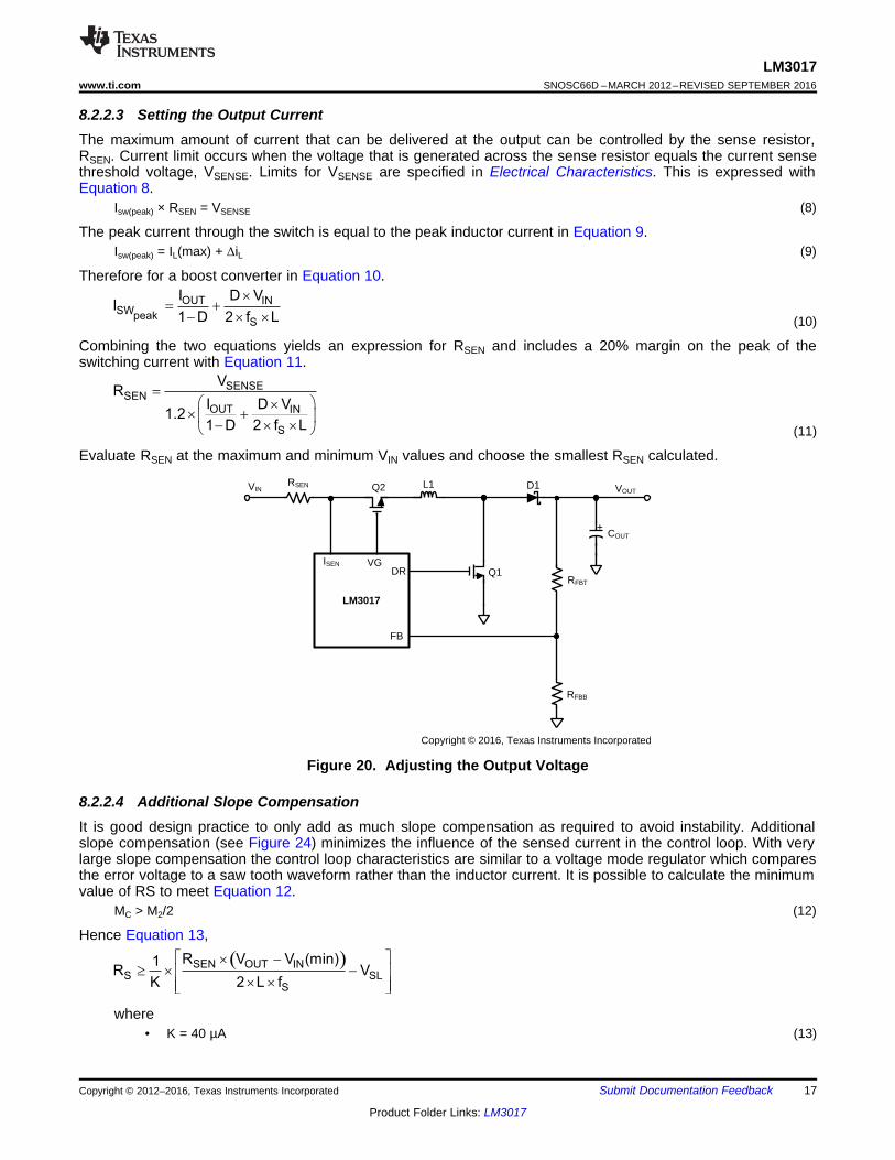
8.2.2.3 Setting the Output CurrentThe maximum amount of current that can be delivered at the output can be controlled by the sense resistor,RSEN. Current limit occurs when the voltage that is generated across the sense resistor equals the current sensethreshold voltage, VSENSE. Limits for VSENSE are specified in Electrical Characteristics. This is expressed withEquation 8.
Isw(peak) × RSEN = VSENSE (8)
The peak current through the switch is equal to the peak inductor current in Equation 9.Isw(peak) = IL(max) + ΔiL (9)
Therefore for a boost converter in Equation 10.
(10)
Combining the two equations yields an expression for RSEN and includes a 20% margin on the peak of theswitching current with Equation 11.
(11)
Evaluate RSEN at the maximum and minimum VIN values and choose the smallest RSEN calculated.
Figure 20. Adjusting the Output Voltage
8.2.2.4 Additional Slope CompensationIt is good design practice to only add as much slope compensation as required to avoid instability. Additionalslope compensation (see Figure 24) minimizes the influence of the sensed current in the control loop. With verylarge slope compensation the control loop characteristics are similar to a voltage mode regulator which comparesthe error voltage to a saw tooth waveform rather than the inductor current. It is possible to calculate the minimumvalue of RS to meet Equation 12.
MC > M2/2 (12)
Hence Equation 13,
where• K = 40 µA (13)

2 2LppOUT
SEN SEN
iIP R
1 D 12
é ùDæ öê ú= ´ +ç ÷
-ê úè øë û
SENSE CSSEN
OUT IN
S
V D VR
I D V
1 D 2 f L
- ´=
æ ö´+ç ÷
- ´ ´è ø
18
LM3017SNOSC66D –MARCH 2012–REVISED SEPTEMBER 2016 www.ti.com
Product Folder Links: LM3017
Submit Documentation Feedback Copyright © 2012–2016, Texas Instruments Incorporated
If the result of the previous equation is negative, it means that no additional slope compensation is required. TIrecommends a 100-Ω resistor.
8.2.2.5 Current Limit With Additional Slope CompensationIf an external slope compensation resistor is used, then the internal control signal is modified and this has aneffect on the current limit.
If RS is used, then this adds to the existing slope compensation. The command voltage, VCS, is then given byEquation 14.
VCS = VSL + ΔVSL
where• VSENSE is a defined parameter in Electrical Characteristics• VSL is the amplitude of the internal compensation ramp• ΔVSL = RS x K is the additional slope compensation generated (14)
This changes the equation for RSEN to Equation 15.
(15)
Because ΔVSL = RS × K as defined earlier, RS can be used to provide an additional method for setting the currentlimit. In some designs RS can also be used to help filter noise to keep the ISEN pin quiet. Dissipation due to RSENresistor is equal to Equation 16.
(16)
8.2.2.6 Power Diode SelectionObservation of the boost converter circuit shows that the average current through the diode is the average outputcurrent, and the peak current through the diode is the peak current through the inductor. The peak diode currentcan be calculated using Equation 17.
ID(Peak) = [IOUT / (1 − D)] + ΔiL (17)
The peak reverse voltage for a boost converter is equal to the regulator output voltage. The diode must becapable of handling this peak reverse voltage as well as the output rms current. To improve efficiency, TIrecommends a low forward drop Schottky diode due to low forward drop and near-zero reverse recovery time.The overall efficiency becomes more dependent on the selection of D at low duty cycles, where the boost diodecarries the load current for an increasing percentage of the time. This power dissipation can be calculated bychecking the typical diode forward voltage VD, from the I-V curve on the diode's datasheet and the multiplying itby IO. Diode data sheets also provides a typical junction-to-ambient thermal resistance, RθJA, which can be usedto estimate the operating die temperature of the Schottky. Multiplying the power dissipation (PD = IO × VD) byRθJA gives the temperature rise. The diode case size can then be selected to maintain the Schottky diodetemperature below the operational maximum.
8.2.2.7 Low-Side MOSFET Selection (Switching MOSFET)The drive pin, DR, of the LM3017 must be connected to the gate of an external MOSFET. In a boost topology,the drain of the external N-Channel MOSFET is connected to the inductor and the source is connected to theground. The drive pin voltage, VDR, depends on the input voltage (see Typical Characteristics).
The selected MOSFET directly affects the efficiency. The critical parameters for selection of a MOSFET are:1. Minimum threshold voltage, VTH(MIN)
2. On-resistance, RDS(ON)
3. Total gate charge, Qg
4. Reverse transfer capacitance, CRSS
5. Maximum drain to source voltage, VDS(MAX)

2 2LppOUT
Q2 DS(on)
iIP R
1 D 12
é ùDæ öê ú= ´ +ç ÷
-ê úè øë û
( ) SC2 in SC
sen
VE V 2 T
R
æ ö³ + ´ ´ç ÷
è ø
( ) LIM21 in LIM2
sen
VE V 2 T
R
æ ö³ + ´ ´ç ÷
è ø
( )L OUTSW S LH HL
I VP f t t
2
´= ´ ´ +
INMAX
OUT
V (min)D 1
V= -
2
OUTCOND MAX DS(on)
MAX
IP D R
1 D
æ ö= ´ ´ç ÷
-è ø
19
LM3017www.ti.com SNOSC66D –MARCH 2012–REVISED SEPTEMBER 2016
Product Folder Links: LM3017
Submit Documentation FeedbackCopyright © 2012–2016, Texas Instruments Incorporated
The off-state voltage of the MOSFET is approximately equal to the output voltage. VDS(MAX) of the MOSFET mustbe greater than the output voltage plus the voltage drop across the output diode (20% margin recommended).
The power losses in the MOSFET can be categorized into conduction losses, gate charging losses and switchinglosses. RDS(ON) is required to estimate the conduction losses. The conduction loss, PCOND, is the I2R loss acrossthe MOSFET. The maximum conduction loss is given by Equation 18 and Equation 19.
where• DMAX is the maximum duty cycle (18)
(19)
To consider the increase in MOSFET on resistance due to heating, a factor of 1.3 is introduced, henceEquation 20.
PCOND_real = PCOND(max) × 1.3 (20)
Gate charging loss, PG, results from the current required to charge and discharge the gate capacitance of thepower MOSFET and is approximated with Equation 21.
PG = VCC × QG fS (21)
QG is the total gate charge of the MOSFET. Gate charge loss differs from conduction and switching lossesbecause the actual dissipation occurs in the LM3017 and not in the MOSFET itself. This loss, PVCC, is estimatedwith Equation 22.
PVCC = (VIN – VCC) × QG × fS (22)
The switching losses are very difficult to calculate due to changing parasitics of a given MOSFET in operation.Often, the individual MOSFET datasheet does not give enough information to yield a useful result. The followingformulas give a rough idea how the switching losses are calculated with Equation 23.
where• tLH and tHL are rise and fall times of the MOSFET (23)
8.2.2.8 Pass MOSFET Selection (High-Side MOSFET)The VG pin drives the gate of the high side MOSFET (Pass FET Q2). This requires special considerations. Whenthe output is shorted, this FET must sustain the full input voltage and the short-circuit current simultaneously.This is due to the fact that the controller regulates the short-circuit current in a quasi-linear manner, through Q2.This power pulse only lasts for TLIM2 or TSC, depending on the operational mode. Therefore, the designer mustcarefully examine the SOA curve for the desired FET before committing to the design. Equation 24 andEquation 25 give the maximum energy pulses that Q2 is required to survive.
(24)
(25)
These two energy points must fall within the SOA of the selected FET. In addition, Q2 must have a low thresholdvoltage and low RDS(on) for high efficiency. Power dissipation during boost mode is given by Equation 26.
(26)

OUT OUTOpp L
o S
I I DV ESR i
1 D C f
´æ öD = ´ + D +ç ÷
- ´è ø
( )OUT
22 L
C (rms) OUT 2
iDI (1 D) I
31 D
é ùDê ú= - ´ ´ +ê ú-ë û
2
2ipp LPP
S i
1V i ESR
8 f C
æ öD = D ´ + ç ÷
´ ´è ø
( )IN
OUT IN INLC (rms)
OUT S
V V ViI
3 12 V f
- ´D= =
´ ´
20
LM3017SNOSC66D –MARCH 2012–REVISED SEPTEMBER 2016 www.ti.com
Product Folder Links: LM3017
Submit Documentation Feedback Copyright © 2012–2016, Texas Instruments Incorporated
8.2.2.9 Input Capacitor SelectionDue to the presence of an inductor at the input of a boost converter, the input current waveform is continuousand triangular. The inductor ensures that the input capacitor sees fairly low ripple currents. However, as the inputcapacitor gets smaller, the input ripple goes up. The rms current in the input capacitor is given by Equation 27.
(27)
The input capacitor must be capable of handling this rms current. Although the input capacitor is not as critical ina boost application, low values can cause impedance interactions. Therefore, a good quality capacitor must bechosen in the range of 10 µF to 20 µF. Furthermore, TI recommends a low-ESR, 0.1-µF ceramic bypasscapacitor to avoid transients and ringing due to parasitics. Bypass capacitors must be placed as close aspossible to the VIN pin and grounded close to the GND pin on the IC to minimize additional ESR and ESL.Equation 28 can be used to define the input voltage ripple.
where• ΔiLpp = 2 × ΔiL is the peak-to-peak inductor current ripple• ΔVipp is the peak-to-peak input voltage ripple (28)
Many times it is necessary to use an electrolytic capacitor on the input in parallel with the ceramics. The ESR ofthis capacitor can help to damp any ringing on the input supply caused by long power leads.
8.2.2.10 Output Capacitor SelectionThe output capacitor in a boost converter provides all the output current when the inductor is charging and itdetermines the steady state output voltage ripple ΔVOpp. As a result it sees very large ripple currents. The outputcapacitor must be selected based on its capacitance CO, its equivalent series resistance ESR and its RMScurrent rating. The rms current in the output capacitor is calculated with Equation 29.
where• ΔiL is the inductor ripple current• D is the duty cycle (29)
The magnitude of the output voltage ripple during the on-time is equal to the ripple voltage during the off-timeand it is composed of two parts. For simplicity, the analysis is performed for off-time only.
The first part of the ripple voltage is the surge created as the output diode D turns on. At this point inductor ordiode current is at the peak value, and the ripple voltage increase can be calculated with Equation 30.
ΔVO1 = IPK × ESR
where• IPK = IOUT / (1 − D) (30)
The second portion of the ripple voltage is the increase due to the charging of CO through the output diode. Thisportion can be approximated with Equation 31.
ΔVO2 = (IO / CO) × (D / fS) (31)
Equation 32 can be used to define the output voltage ripple.
(32)

VOUT PsOpp
ID
VOUT PsOpp
ID
21
LM3017www.ti.com SNOSC66D –MARCH 2012–REVISED SEPTEMBER 2016
Product Folder Links: LM3017
Submit Documentation FeedbackCopyright © 2012–2016, Texas Instruments Incorporated
The ESR of the output capacitor(s) has a strong influence on the slope and direction of the output voltage ripple.Capacitors with high ESR such as tantalum and aluminum electrolytic create an output voltage ripple that isdominated by ΔVO1 with a shape shown in Figure 21. Ceramic capacitors, in contrast, have a very low ESR andlower capacitance, and the shape of the output voltage ripple is dominated by ΔVO2 with a shape shown inFigure 22.
Figure 21. ΔVOpp Using High ESR Capacitors Figure 22. ΔVOpp Using Low ESR CapacitorsCeramic capacitors are recommended with a typical value from 10 µF to 100 µF. The minimum quality dielectricthat is suitable for switching power supply output capacitors is X5R, while X7R (or better) is preferred. Carefulattention must be paid to the DC voltage rating and case size, as ceramic capacitors can lose 60% or more oftheir rated capacitance at the maximum DC voltage. This is the reason that ceramic capacitors often derate to50% of their capacitance at their working voltage.
8.2.2.11 VCC Decoupling CapacitorThe internal bias of the LM3017 comes from either the internal bias voltage generator as shown in the blockdiagram or directly from the voltage at the VIN pin. At input voltages lower than 6 V, the internal IC bias is theinput voltage and at voltages above 6 V the internal bias voltage generator of the LM3017 provides the bias. Agood quality ceramic bypass capacitor must be connected from the VCC pin to the PGND pin for properoperation. This capacitor supplies the transient current required by the internal MOSFET driver, as well asfiltering the internal supply voltage for the controller. TI recommends a value of between 0.47 µF and 4.7 µF.
8.2.2.12 Slope Compensation RampThe LM3017 uses a current mode control scheme. The main advantages of current mode control are inherentcycle-by-cycle current limit for the switch, simpler control loop characteristics and excellent line and load transientresponse. However, there is a natural instability due to subharmornic oscillations that occurs for duty cycles, D,greater than 50% if slope compensation is not addressed in Equation 33.
MC > M2 / 2 (33)
For best input noise immunity, use Equation 34.MC = M2 (34)
For best sub-harmonic suppression, use Equation 35.MC = M2 / 2
where• MC is the slope of the compensation ramp• M1 is the slope of the inductor current during the ON time• M2 is the slope of the inductor current during the OFF time• RSEN is the sensing resistor value• VOUT represents the output voltage• VIN represents the input voltage• A is equal to 0.86 and it is the internal sensing amplification of the LM3017 (35)
In the case of the boost topology, use Equation 36 and Equation 37.

LM3017
DRISEN
VINL1
VG
RSEN
Q2
RSCS
Copyright © 2016, Texas Instruments Incorporated
Control Signal Compensation Rampwithout RSL
-MC
VSL
'VSL
Control Signal Compensation Ramp
with RSL
22
LM3017SNOSC66D –MARCH 2012–REVISED SEPTEMBER 2016 www.ti.com
Product Folder Links: LM3017
Submit Documentation Feedback Copyright © 2012–2016, Texas Instruments Incorporated
M1 = [VIN / L] × RSEN × A (36)M2 = [(VOUT – VIN) / L] × RSEN × A (37)
The compensation ramp is added internally in the LM3017. The slope of this compensation ramp is selected tosatisfy most applications, and its value depends on the switching frequency. This slope can be calculated usingEquation 38.
MC = VSL × fS (38)
In the above equation, VSL is the amplitude of the internal compensation ramp and fS is the controller's switchingfrequency. Limits for VSL are specified in Electrical Characteristics.
To provide the user additional flexibility, a patented scheme is implemented inside the IC to increase the slope ofthe compensation ramp externally, if the requirement arises. Adding a single external resistor, RS (as shown inFigure 24) increases the amplitude of the compensation ramp as shown in Figure 23 where Equation 39.
Figure 23. Additional Slope Compensation Added Using External Resistor RS
ΔVSL = K × Rs
where• K = 40 µA typically and changes slightly as the switching frequency changes (39)
A more general equation for the slope compensation ramp, MC, is shown in Equation 40 to include ΔVSL causedby the resistor, Rs.
MC = (VSL + ΔVSL) × fs (40)
Figure 24. Increasing the Slope of the Compensation Ramp
An additional capacitor, CS, could be added if the sensing signal generated by RSEN is very noisy (parasitic circuitcapacitance, inductance, and gate drive current create a spike in the current sense voltage at the point where Q1turns on). The time constant RSEN x CS must be long enough to reduce the parasitics spike without significantlyaffecting the shape of the actual current sense voltage (a typical range is from 100 pF to 2.2 nF).

( )2
ORR
R 1 Df
2 2 L
´ -w= =
p p ´
( )P
P
O O
2f
2 2 C ESR R
w= =
p p ´ ´ +
ZZ
O
1f
2 2 C ESR
w
= =
p p ´ ´
OVC0
SEN
R (1 D)G
2 A R
-
=
´ ´
R ZVC VC0 2
2P n n
s s1 1
G (s) Gs s s
1 1
æ öæ ö- +ç ÷ç ÷
w wè øè ø= ´æ öæ ö
+ + +ç ÷ç ÷ç ÷w w wè øè ø
+-
+D
VREF+-
L
CO
ROVIN
ESR
RFBT
RFBB
RSEN
+-
CCOMP
RCOMP
CCOMP2
+ -
Current SenseAmp.
+ -
A
23
LM3017www.ti.com SNOSC66D –MARCH 2012–REVISED SEPTEMBER 2016
Product Folder Links: LM3017
Submit Documentation FeedbackCopyright © 2012–2016, Texas Instruments Incorporated
8.2.2.13 Control Loop CompensationThe LM3017 uses peak current-mode PWM control to correct changes in output voltage due to line and loadtransients. Peak current-mode provides inherent cycle-by-cycle current limiting, improved line transient response,and easier control loop compensation. The control loop is comprised of two parts. The first is the power stage,which consists of the pulse width modulator, output filter, and the load. The second part is the error amplifier.Figure 25 shows the regulator control loop components.
Figure 25. Power Stage and Error Amp
The power stage in a CCM peak current mode boost converter consists of the DC gain, GVC0, a single lowfrequency pole, fP, the ESR zero, fZ, a right-half plane zero, fR, and a double pole resulting from the sampling ofthe peak current. The power stage transfer function (also called the Control-to-Output transfer function) can bewritten with Equation 41.
(41)
The DC gain is defined with Equation 42.
where• RO = VOUT / IOUT (42)
In the equation for GVC0, DC gain is highest when input voltage and output current are at the maximum. Thesystem ESR zero is defined with Equation 43.
(43)
The low frequency pole is Equation 44.
(44)
The right-half plane zero is Equation 45.
(45)

FB INm COMP
OUT OUT C O SEN
V V 1 1| T | G R 1
V V 2 f C A R= ´ ´ ´ ´ ´ =
p ´ ´ ´
RC
ff
5£
COMP COMP2P2
COMP COMP2 COMP
C C
C C R
+
w =
´ ´
FBBm
FBB FBTP1
COMP COMP2
RG
R R
C C
´
+
w =
+
Z1
COMP COMP
1
C Rw =
´
P1Z1
VA
P2
s1
G (s)s
s 1
æ öw +ç ÷
wè ø=æ ö
+ç ÷wè ø
( )n
C
1
1Q
M1 D 1 0.5
M
=é ùæ ö
p ´ - ´ + -ê úç ÷ê úè øë û
24
LM3017SNOSC66D –MARCH 2012–REVISED SEPTEMBER 2016 www.ti.com
Product Folder Links: LM3017
Submit Documentation Feedback Copyright © 2012–2016, Texas Instruments Incorporated
The sampling double pole quality factor is Equation 46.
(46)
The sampling double corner frequency is Equation 47.ωn = π × fS (47)
The natural inductor current slope is Equation 48.M1 = RSEN × VIN / L (48)
The external ramp slope is Equation 49.MC = (VSL + ΔVSL) × fS (49)
A step-up converter produces an undesirable right-half plane zero in the regulation feedback loop. This requirescompensating the regulator such that the crossover frequency occurs well below the frequency of the right-halfplane zero
8.2.2.13.1 Compensation Network Components Calculations
As shown in Figure 25, the LM3017 uses a compensation network base on a transconductance amplifier. Theclosed-loop transfer function is defined with Equation 50 through Equation 54.
T(s) = GVA(s) × GVC(s)
where• GVA(s) is the transfer function implemented by the compensation network (50)
(51)
(52)
(53)
(54)
To stabilize the regulator, ensure that the regulator crossover frequency is less than or equal to one-fifth of theright-half plane zero with Equation 55.
(55)
To determine the crossover frequency it is important to note that, at that frequency, the compensation impedance(ZCOMP) is dominated by a resistor, and the output impedance (ZOUT) is dominated by the impedance of an outputcapacitor. Therefore, when solving for the crossover frequency, the equation (by definition of the crossoverfrequency) of the loop gain is simplified to Equation 56.
where• |T| is the loop gain magnitude• VFB is feedback voltage, 1.275 V• VOUT is the output voltage• VIN is the input voltage

OCOMP2
COMP
ESR CC
R
´
=
COMP
C COMP
2C
f R=
p ´ ´
2
C O OUTCOMP SEN
FB IN m
2 f C VR A R
V V G
p ´ ´ ´
= ´ ´
´ ´
25
LM3017www.ti.com SNOSC66D –MARCH 2012–REVISED SEPTEMBER 2016
Product Folder Links: LM3017
Submit Documentation FeedbackCopyright © 2012–2016, Texas Instruments Incorporated
• Gm is the error amplifier transconductance• ZCOMP is the impedance of the compensation network from the COMP pin to ground• RSEN is the current sensing resistor• A is equal to 0.86 and it is the internal sensing amplification of the LM3017• CO is the output capacitor value (56)
Solve for RCOMP with Equation 57.
(57)
Once the compensation resistor is known, set the zero formed by the compensation capacitor and resistor toone-fourth of the crossover frequency in Equation 58.
where• CCOMP is the compensation capacitor (58)
The high-frequency capacitor CCOMP2, is chosen to cancel the zero introduced by output capacitance ESR withEquation 59.
(59)
For optimal transient performance, RCOMP and CCOMP might require adjustment by observing the load transientresponse.
For detailed explanation on how to select the right compensation components for a boost topology, see AN-1286Compensation for the LM3478 Boost Controller (SNVA067), and AN-1994 Modeling and Design of Current ModeControl Boost Converters (SNVA408).
8.2.2.13.2 Compensation Design Example
Table 3 lists the design parameters for this application example to calculate the compensation network.
Table 3. Design ParametersPARAMETER VALUE
Input voltage, VIN 8 V to 12 VOutput voltage, VOUT 15 VOutput current, IOUT 1 A
Switching frequency, fS 600 kHz
Duty cycle, D(considering losses)
0.482 with VIN = 8 V0.223 with VIN = 12 V
Right-half plane zero, fR136.187 kHz when VIN = 8 V
206.421 kHz when VIN = 12 VInductor, L 4.7 µH
Output capacitance, CO(considering derating due to
applied voltage)33 µF

26
LM3017SNOSC66D –MARCH 2012–REVISED SEPTEMBER 2016 www.ti.com
Product Folder Links: LM3017
Submit Documentation Feedback Copyright © 2012–2016, Texas Instruments Incorporated
space
VIN = 8 V, VOUT = 15 V, IOUT = 1 AFigure 26. Control-to-Output Transfer Function
GVC(s) Bode PlotChoose the crossover frequency with Equation 60.
fC = 20 kHz = fS / 20 fR / 5 (60)
Table 4. Calculated Compensation Network ComponentsPARAMETER CALCULATED VALUE ACTUAL VALUE
RCOMP 3.42 kΩ 3.4 kΩCCOMP 9.306 nF 10 nFCCOMP2 96.48 pF 100 pF
space
VIN = 8 V, VOUT = 15 V, IOUT = 1 A VIN = 8 V, VOUT = 15 V, IOUT = 1 A
Figure 27. GVC(s) and Compensation NetworkGVA(s) Bode Plots
Figure 28. Closed-Loop Bode Plot T(s)
Table 5. Bill of Materials (BOM) for LM3017DESIGNATION DESCRIPTION SIZE MANUFACTURER PART # VENDOR
CIN1 Cap 22 µF, 25 V X5R 1206 GRM31CR61E226KE15L Murata
CO1,CO2, CO3 Cap 22 µF, 25 V X5R 1206 GRM31CR61E226KE15L Murata
CCOMP Cap 0.022 µF 0603 C0603C103J1RACTU Kemet
CCOMP2 Cap 1000 pF 0603 C1608C0G1H101J TDK
CBYP Cap 0.1 µF, 25 V X7R 0603 06033C104KAT2A AVX
CVCC Cap 0.47 µF, 16 V X7R 0805 C2012X7R1C474K TDK
RCOMP RES, 3.4 kΩ, 1%, 0.1W 0603 CRCW06033K40FKEA Vishay

27
LM3017www.ti.com SNOSC66D –MARCH 2012–REVISED SEPTEMBER 2016
Product Folder Links: LM3017
Submit Documentation FeedbackCopyright © 2012–2016, Texas Instruments Incorporated
Table 5. Bill of Materials (BOM) for LM3017 (continued)DESIGNATION DESCRIPTION SIZE MANUFACTURER PART # VENDOR
RFBT RES, 21.5 kΩ, 1%, 0.1W 0603 CRCW060321K5FKEA Vishay
RFBB RES, 2 kΩ, 1%, 0.1W 0603 CRCW06032K00FKEA Vishay
RS RES, 100 Ω, 1%, 0.1W 0603 CRCW0603100RFKEA Vishay
RSEN RES, 0.03 Ω, 1%, 1W 1206 WSLP1206R0300FEA Vishay
Q1 NexFET™ N-CH, 25 V, 60 A, RDS(on)= 4.4 mΩ 8-SON CSD16323Q3 TI
Q2 NexFET™ N-CH, 25 V, 60 A, RDS(on)= 4.3 mΩ 8-SON CSD16340Q3 TI
D1 Diode Schottky, 30 V, 2 A SMB 20BQ030TRPBF Vishay
L1 Shielded Inductor, 4.7 µH, 2.3 A 4 mm L × 4 mm W × 1.85 mm H MPI4040R3-4R7-R Cooper
U1 LM3017 — — TI
8.2.3 Application Curve
Figure 29. Switch Node and Output Voltage RippleWith 5.5 VIN and 15 V at 1-A Output

28
LM3017SNOSC66D –MARCH 2012–REVISED SEPTEMBER 2016 www.ti.com
Product Folder Links: LM3017
Submit Documentation Feedback Copyright © 2012–2016, Texas Instruments Incorporated
9 Power Supply RecommendationsThe LM3017 is designed to operate from an input voltage supply range from 5 V to 18 V. This input supply mustbe able to withstand the maximum input current and maintain a voltage above 5 V. In cases where input supplyis placed farther away (more than a few inches) from LM3017, additional bulk capacitance may be required inaddition to the ceramic bypass capacitors.
10 Layout
10.1 Layout GuidelinesGood board layout is critical for switching controllers such as the LM3017. First the ground plane area must besufficient for thermal dissipation purposes and second, appropriate guidelines must be followed to reduce theeffects of switching noise. Switch mode converters are very fast switching devices. In such devices, the rapidincrease of input current combined with the parasitic trace inductance generates unwanted voltage noise spikes.The magnitude of this noise tends to increase as the output current increases. This parasitic spike noise maycreate electromagnetic interference (EMI), and can also cause problems in device performance. Therefore, takecare in layout to minimize the effect of this switching noise.
10.1.1 Filter CapacitorsCeramic filter capacitors are most effective when the inductance of the current loops that they filter is minimized.Place CBYP as close as possible to the VIN and GND pins of the LM3017. Place CVCC next to the VCC and GNDpins of the LM3017 (see Figure 16 for designators).
10.1.2 Sense LinesThe current sensing circuit in current mode devices can be easily effected by switching noise. This noise cancause duty cycle jitter which leads to increased spectral noise. RSEN must be connected to the ISEN pin with aseparate trace made as short as possible, TI also recommends to route the trace that connects the VIN pin tothe input voltage as close as possible to RSEN. Route this trace away from the inductor and the switch node(where D1, Q1, and L1 connect). For the voltage loop, keep RFBB/T close to the LM3017 and run a trace as closeas possible to the positive side of CO. As with the ISEN line, the FB line must be routed away from the inductorand the switch node. These measures minimize the length of high impedance lines and reduce noise pickup.
10.1.3 Compact LayoutThe most important layout rule is to keep the AC current loops as small as possible. Figure 30 shows the currentflow of a boost converter. The top schematic shows a dotted line which represents the current flow during on-state and the middle schematic shows the current flow during off-state. The bottom schematic shows the currentsreferred to as AC currents. They are the most critical ones because current is changing in very short timeperiods. The dotted line traces of the bottom schematic are the ones to make as short as possible. In a boostregulator the primary switching loop consists of the output capacitor, diode and MOSFET. Minimizing the area ofthis loop reduces the stray inductances and minimizes noise and possible erratic operation (see LayoutExamples). The output capacitor(s) must be placed as close as possible to the diode cathode and MOSFETGND.

29
LM3017www.ti.com SNOSC66D –MARCH 2012–REVISED SEPTEMBER 2016
Product Folder Links: LM3017
Submit Documentation FeedbackCopyright © 2012–2016, Texas Instruments Incorporated
Layout Guidelines (continued)
Figure 30. Current Flow in a Boost Application
10.1.4 Ground Plane and ViasA ground plane in the printed-circuit board is recommended as a means to connect the quiet end (input voltageground side) of the input filter capacitor to the output filter capacitors and the PGND pin of the controller. Connectall the low power ground connections directly to the regulator AGND. Connect the AGND and PGND pinstogether through a copper area covering the entire underside of the device. Place several vias in this undersidecopper area to ground plane. If a via is required to connect the sensing resistor to the ISEN pin, then place thatvia in the inner side of the sensing resistor such that no current flow occurs. Place several vias from the groundside of the output capacitor(s) to ground place, that minimizes the path for AC current. The PGND and AGNDpins have to be connected to the same ground very close to the IC. To avoid ground loop currents attach all thegrounds of the system only at one point.
30
LM3017SNOSC66D –MARCH 2012–REVISED SEPTEMBER 2016 www.ti.com
Product Folder Links: LM3017
Submit Documentation Feedback Copyright © 2012–2016, Texas Instruments Incorporated
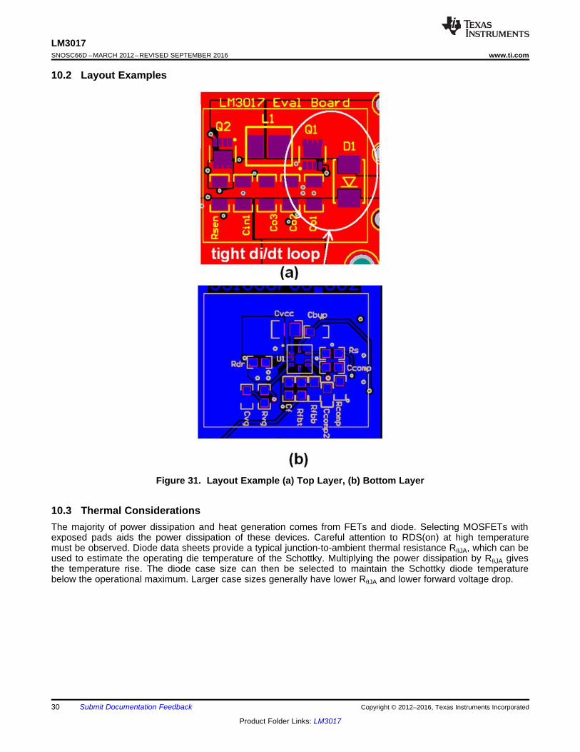
10.2 Layout Examples
Figure 31. Layout Example (a) Top Layer, (b) Bottom Layer
10.3 Thermal ConsiderationsThe majority of power dissipation and heat generation comes from FETs and diode. Selecting MOSFETs withexposed pads aids the power dissipation of these devices. Careful attention to RDS(on) at high temperaturemust be observed. Diode data sheets provide a typical junction-to-ambient thermal resistance RθJA, which can beused to estimate the operating die temperature of the Schottky. Multiplying the power dissipation by RθJA givesthe temperature rise. The diode case size can then be selected to maintain the Schottky diode temperaturebelow the operational maximum. Larger case sizes generally have lower RθJA and lower forward voltage drop.

31
LM3017www.ti.com SNOSC66D –MARCH 2012–REVISED SEPTEMBER 2016
Product Folder Links: LM3017
Submit Documentation FeedbackCopyright © 2012–2016, Texas Instruments Incorporated
11 Device and Documentation Support
11.1 Documentation Support
11.1.1 Related DocumentationFor related documentation see the following:• AN-1286 Compensation for the LM3478 Boost Controller (SNVA067)• AN-1994 Modeling and Design of Current Mode Control Boost Converters (SNVA408)
11.2 Receiving Notification of Documentation UpdatesTo receive notification of documentation updates, navigate to the device product folder on ti.com. In the upperright corner, click on Alert me to register and receive a weekly digest of any product information that haschanged. For change details, review the revision history included in any revised document.
11.3 Community ResourcesThe following links connect to TI community resources. Linked contents are provided "AS IS" by the respectivecontributors. They do not constitute TI specifications and do not necessarily reflect TI's views; see TI's Terms ofUse.
TI E2E™ Online Community TI's Engineer-to-Engineer (E2E) Community. Created to foster collaborationamong engineers. At e2e.ti.com, you can ask questions, share knowledge, explore ideas and helpsolve problems with fellow engineers.
Design Support TI's Design Support Quickly find helpful E2E forums along with design support tools andcontact information for technical support.
11.4 TrademarksE2E is a trademark of Texas Instruments.Thunderbolt is a trademark of Intel Corporation.All other trademarks are the property of their respective owners.
11.5 Electrostatic Discharge CautionThese devices have limited built-in ESD protection. The leads should be shorted together or the device placed in conductive foamduring storage or handling to prevent electrostatic damage to the MOS gates.
11.6 GlossarySLYZ022 — TI Glossary.
This glossary lists and explains terms, acronyms, and definitions.
12 Mechanical, Packaging, and Orderable InformationThe following pages include mechanical, packaging, and orderable information. This information is the mostcurrent data available for the designated devices. This data is subject to change without notice and revision ofthis document. For browser-based versions of this data sheet, refer to the left-hand navigation.

PACKAGE OPTION ADDENDUM
www.ti.com 24-Feb-2017
Addendum-Page 1
PACKAGING INFORMATION
Orderable Device Status(1)
Package Type PackageDrawing
Pins PackageQty
Eco Plan(2)
Lead/Ball Finish(6)
MSL Peak Temp(3)
Op Temp (°C) Device Marking(4/5)
Samples
LM3017LE/NOPB ACTIVE WQFN NKL 10 1000 Green (RoHS& no Sb/Br)
CU SN Level-3-260C-168 HR -40 to 125 SK6B
LM3017LEX/NOPB ACTIVE WQFN NKL 10 4500 Green (RoHS& no Sb/Br)
CU SN Level-3-260C-168 HR -40 to 125 SK6B
(1) The marketing status values are defined as follows:ACTIVE: Product device recommended for new designs.LIFEBUY: TI has announced that the device will be discontinued, and a lifetime-buy period is in effect.NRND: Not recommended for new designs. Device is in production to support existing customers, but TI does not recommend using this part in a new design.PREVIEW: Device has been announced but is not in production. Samples may or may not be available.OBSOLETE: TI has discontinued the production of the device.
(2) Eco Plan - The planned eco-friendly classification: Pb-Free (RoHS), Pb-Free (RoHS Exempt), or Green (RoHS & no Sb/Br) - please check http://www.ti.com/productcontent for the latest availabilityinformation and additional product content details.TBD: The Pb-Free/Green conversion plan has not been defined.Pb-Free (RoHS): TI's terms "Lead-Free" or "Pb-Free" mean semiconductor products that are compatible with the current RoHS requirements for all 6 substances, including the requirement thatlead not exceed 0.1% by weight in homogeneous materials. Where designed to be soldered at high temperatures, TI Pb-Free products are suitable for use in specified lead-free processes.Pb-Free (RoHS Exempt): This component has a RoHS exemption for either 1) lead-based flip-chip solder bumps used between the die and package, or 2) lead-based die adhesive used betweenthe die and leadframe. The component is otherwise considered Pb-Free (RoHS compatible) as defined above.Green (RoHS & no Sb/Br): TI defines "Green" to mean Pb-Free (RoHS compatible), and free of Bromine (Br) and Antimony (Sb) based flame retardants (Br or Sb do not exceed 0.1% by weightin homogeneous material)
(3) MSL, Peak Temp. - The Moisture Sensitivity Level rating according to the JEDEC industry standard classifications, and peak solder temperature.
(4) There may be additional marking, which relates to the logo, the lot trace code information, or the environmental category on the device.
(5) Multiple Device Markings will be inside parentheses. Only one Device Marking contained in parentheses and separated by a "~" will appear on a device. If a line is indented then it is a continuationof the previous line and the two combined represent the entire Device Marking for that device.
(6) Lead/Ball Finish - Orderable Devices may have multiple material finish options. Finish options are separated by a vertical ruled line. Lead/Ball Finish values may wrap to two lines if the finishvalue exceeds the maximum column width.
Important Information and Disclaimer:The information provided on this page represents TI's knowledge and belief as of the date that it is provided. TI bases its knowledge and belief on informationprovided by third parties, and makes no representation or warranty as to the accuracy of such information. Efforts are underway to better integrate information from third parties. TI has taken andcontinues to take reasonable steps to provide representative and accurate information but may not have conducted destructive testing or chemical analysis on incoming materials and chemicals.TI and TI suppliers consider certain information to be proprietary, and thus CAS numbers and other limited information may not be available for release.

PACKAGE OPTION ADDENDUM
www.ti.com 24-Feb-2017
Addendum-Page 2
In no event shall TI's liability arising out of such information exceed the total purchase price of the TI part(s) at issue in this document sold by TI to Customer on an annual basis.

TAPE AND REEL INFORMATION
*All dimensions are nominal
Device PackageType
PackageDrawing
Pins SPQ ReelDiameter
(mm)
ReelWidth
W1 (mm)
A0(mm)
B0(mm)
K0(mm)
P1(mm)
W(mm)
Pin1Quadrant
LM3017LE/NOPB WQFN NKL 10 1000 178.0 12.4 2.7 3.0 1.0 8.0 12.0 Q1
LM3017LEX/NOPB WQFN NKL 10 4500 330.0 12.4 2.7 3.0 1.0 8.0 12.0 Q1
PACKAGE MATERIALS INFORMATION
www.ti.com 20-Sep-2016
Pack Materials-Page 1

*All dimensions are nominal
Device Package Type Package Drawing Pins SPQ Length (mm) Width (mm) Height (mm)
LM3017LE/NOPB WQFN NKL 10 1000 210.0 185.0 35.0
LM3017LEX/NOPB WQFN NKL 10 4500 367.0 367.0 35.0
PACKAGE MATERIALS INFORMATION
www.ti.com 20-Sep-2016
Pack Materials-Page 2
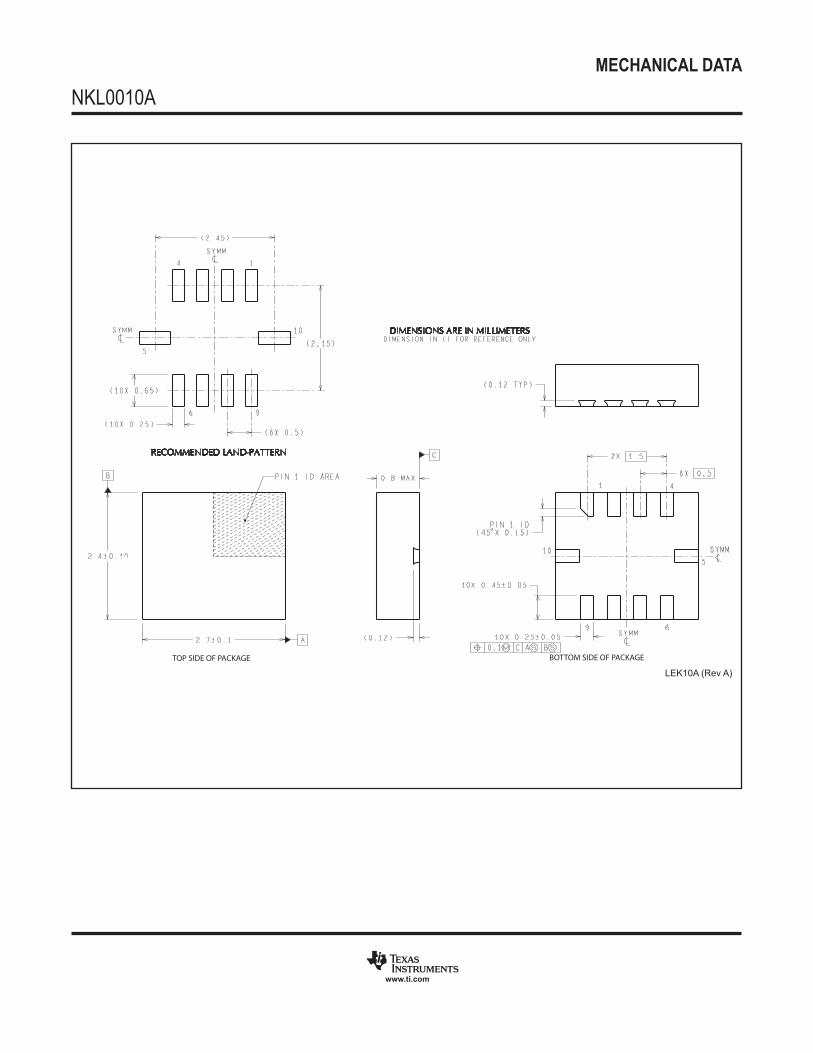
MECHANICAL DATA
NKL0010A
www.ti.com
LEK10A (Rev A)
TOP SIDE OF PACKAGE BOTTOM SIDE OF PACKAGE

IMPORTANT NOTICE
Texas Instruments Incorporated (TI) reserves the right to make corrections, enhancements, improvements and other changes to itssemiconductor products and services per JESD46, latest issue, and to discontinue any product or service per JESD48, latest issue. Buyersshould obtain the latest relevant information before placing orders and should verify that such information is current and complete.TI’s published terms of sale for semiconductor products (http://www.ti.com/sc/docs/stdterms.htm) apply to the sale of packaged integratedcircuit products that TI has qualified and released to market. Additional terms may apply to the use or sale of other types of TI products andservices.Reproduction of significant portions of TI information in TI data sheets is permissible only if reproduction is without alteration and isaccompanied by all associated warranties, conditions, limitations, and notices. TI is not responsible or liable for such reproduceddocumentation. Information of third parties may be subject to additional restrictions. Resale of TI products or services with statementsdifferent from or beyond the parameters stated by TI for that product or service voids all express and any implied warranties for theassociated TI product or service and is an unfair and deceptive business practice. TI is not responsible or liable for any such statements.Buyers and others who are developing systems that incorporate TI products (collectively, “Designers”) understand and agree that Designersremain responsible for using their independent analysis, evaluation and judgment in designing their applications and that Designers havefull and exclusive responsibility to assure the safety of Designers' applications and compliance of their applications (and of all TI productsused in or for Designers’ applications) with all applicable regulations, laws and other applicable requirements. Designer represents that, withrespect to their applications, Designer has all the necessary expertise to create and implement safeguards that (1) anticipate dangerousconsequences of failures, (2) monitor failures and their consequences, and (3) lessen the likelihood of failures that might cause harm andtake appropriate actions. Designer agrees that prior to using or distributing any applications that include TI products, Designer willthoroughly test such applications and the functionality of such TI products as used in such applications.TI’s provision of technical, application or other design advice, quality characterization, reliability data or other services or information,including, but not limited to, reference designs and materials relating to evaluation modules, (collectively, “TI Resources”) are intended toassist designers who are developing applications that incorporate TI products; by downloading, accessing or using TI Resources in anyway, Designer (individually or, if Designer is acting on behalf of a company, Designer’s company) agrees to use any particular TI Resourcesolely for this purpose and subject to the terms of this Notice.TI’s provision of TI Resources does not expand or otherwise alter TI’s applicable published warranties or warranty disclaimers for TIproducts, and no additional obligations or liabilities arise from TI providing such TI Resources. TI reserves the right to make corrections,enhancements, improvements and other changes to its TI Resources. TI has not conducted any testing other than that specificallydescribed in the published documentation for a particular TI Resource.Designer is authorized to use, copy and modify any individual TI Resource only in connection with the development of applications thatinclude the TI product(s) identified in such TI Resource. NO OTHER LICENSE, EXPRESS OR IMPLIED, BY ESTOPPEL OR OTHERWISETO ANY OTHER TI INTELLECTUAL PROPERTY RIGHT, AND NO LICENSE TO ANY TECHNOLOGY OR INTELLECTUAL PROPERTYRIGHT OF TI OR ANY THIRD PARTY IS GRANTED HEREIN, including but not limited to any patent right, copyright, mask work right, orother intellectual property right relating to any combination, machine, or process in which TI products or services are used. Informationregarding or referencing third-party products or services does not constitute a license to use such products or services, or a warranty orendorsement thereof. Use of TI Resources may require a license from a third party under the patents or other intellectual property of thethird party, or a license from TI under the patents or other intellectual property of TI.TI RESOURCES ARE PROVIDED “AS IS” AND WITH ALL FAULTS. TI DISCLAIMS ALL OTHER WARRANTIES ORREPRESENTATIONS, EXPRESS OR IMPLIED, REGARDING RESOURCES OR USE THEREOF, INCLUDING BUT NOT LIMITED TOACCURACY OR COMPLETENESS, TITLE, ANY EPIDEMIC FAILURE WARRANTY AND ANY IMPLIED WARRANTIES OFMERCHANTABILITY, FITNESS FOR A PARTICULAR PURPOSE, AND NON-INFRINGEMENT OF ANY THIRD PARTY INTELLECTUALPROPERTY RIGHTS. TI SHALL NOT BE LIABLE FOR AND SHALL NOT DEFEND OR INDEMNIFY DESIGNER AGAINST ANY CLAIM,INCLUDING BUT NOT LIMITED TO ANY INFRINGEMENT CLAIM THAT RELATES TO OR IS BASED ON ANY COMBINATION OFPRODUCTS EVEN IF DESCRIBED IN TI RESOURCES OR OTHERWISE. IN NO EVENT SHALL TI BE LIABLE FOR ANY ACTUAL,DIRECT, SPECIAL, COLLATERAL, INDIRECT, PUNITIVE, INCIDENTAL, CONSEQUENTIAL OR EXEMPLARY DAMAGES INCONNECTION WITH OR ARISING OUT OF TI RESOURCES OR USE THEREOF, AND REGARDLESS OF WHETHER TI HAS BEENADVISED OF THE POSSIBILITY OF SUCH DAMAGES.Unless TI has explicitly designated an individual product as meeting the requirements of a particular industry standard (e.g., ISO/TS 16949and ISO 26262), TI is not responsible for any failure to meet such industry standard requirements.Where TI specifically promotes products as facilitating functional safety or as compliant with industry functional safety standards, suchproducts are intended to help enable customers to design and create their own applications that meet applicable functional safety standardsand requirements. Using products in an application does not by itself establish any safety features in the application. Designers mustensure compliance with safety-related requirements and standards applicable to their applications. Designer may not use any TI products inlife-critical medical equipment unless authorized officers of the parties have executed a special contract specifically governing such use.Life-critical medical equipment is medical equipment where failure of such equipment would cause serious bodily injury or death (e.g., lifesupport, pacemakers, defibrillators, heart pumps, neurostimulators, and implantables). Such equipment includes, without limitation, allmedical devices identified by the U.S. Food and Drug Administration as Class III devices and equivalent classifications outside the U.S.TI may expressly designate certain products as completing a particular qualification (e.g., Q100, Military Grade, or Enhanced Product).Designers agree that it has the necessary expertise to select the product with the appropriate qualification designation for their applicationsand that proper product selection is at Designers’ own risk. Designers are solely responsible for compliance with all legal and regulatoryrequirements in connection with such selection.Designer will fully indemnify TI and its representatives against any damages, costs, losses, and/or liabilities arising out of Designer’s non-compliance with the terms and provisions of this Notice.
Mailing Address: Texas Instruments, Post Office Box 655303, Dallas, Texas 75265Copyright © 2017, Texas Instruments Incorporated