High efficiency DC-DC Converter Fed, reduced Switch, 5 level Sine PWM INVERTER for PV applications
27
Tribute to the great Scientist Nikola Tesla
-
Upload
ranjith1890 -
Category
Design
-
view
167 -
download
1
Transcript of High efficiency DC-DC Converter Fed, reduced Switch, 5 level Sine PWM INVERTER for PV applications

Tribute to the great Scientist
Nikola Tesla
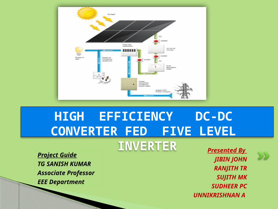
Presented By JIBIN JOHN
RANJITH TRSUJITH MK
SUDHEER PCUNNIKRISHNAN A
HIGH EFFICIENCY DC-DC CONVERTER FED FIVE LEVEL
INVERTERProject GuideTG SANISH KUMARAssociate ProfessorEEE Department
We are discussing with,
1.Why High efficiency Inverter system2.Wide input high efficiency high step-up Dc- Dc Converter
o Modes of operation3.Reduced switch 5 level inverter
o Modes of operation4. Integrated inverter system with high efficiency converter
o Simulation diagramo Simulation resulto Analysis
5.Hardware Implementationo Schematic Diagramo Top view of PCBo Hardware Result
6.Conclusion and future scope05/03/2023 3

05/03/2023 4
WHY HIGH EFFICIENCY INVERTER SYSTEM
Energy plays a pivotal role in our life daily activities. Energy demand is increasing day be day due to increase
in population urbanization and industrialization The worlds fossil fuel supply will thus depleted in a few
hundred years Result will be inflation and energy shortage Hence we the engineers have to take the responsibility
to use the renewable source in efficient manner For this Efficient power converts has an important role
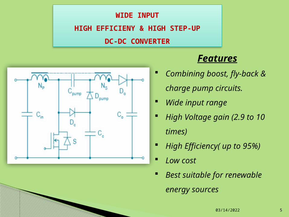
WIDE INPUT HIGH EFFICIENY & HIGH STEP-UP
DC-DC CONVERTER
Features Combining boost, fly-back &
charge pump circuits. Wide input range High Voltage gain (2.9 to 10
times) High Efficiency( up to 95%) Low cost Best suitable for renewable
energy sources
05/03/2023 5
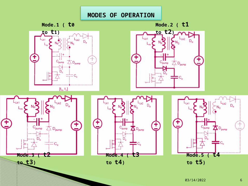
MODES OF OPERATION
05/03/2023 6
Mode.1 ( t0 to t1) Mode.2 ( t1 to t2)
Mode.3 ( t2 to t3) Mode.4 ( t3 to t4) Mode.5 ( t4 to t5)
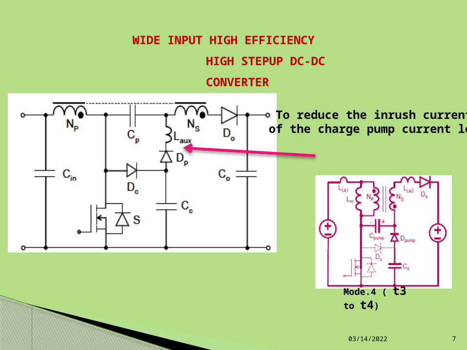
05/03/2023 7
Mode.4 ( t3 to t4)
To reduce the inrush current of the charge pump current loop
WIDE INPUT HIGH EFFICIENCY HIGH STEPUP DC-DC
CONVERTER
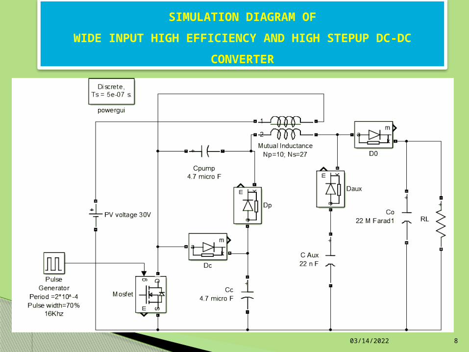
SIMULATION DIAGRAM OFWIDE INPUT HIGH EFFICIENCY AND HIGH STEPUP DC-DC
CONVERTER
05/03/2023 8
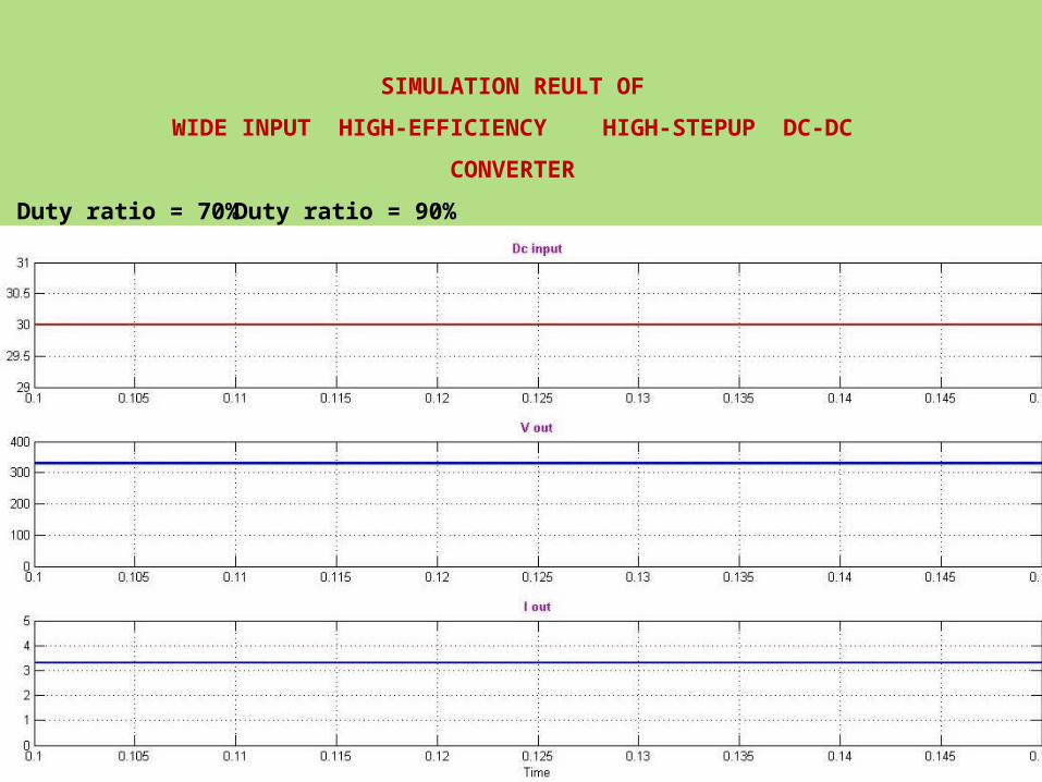
SIMULATION REULT OFWIDE INPUT HIGH-EFFICIENCY HIGH-STEPUP DC-DC
CONVERTERDuty ratio = 70% Duty ratio = 90%
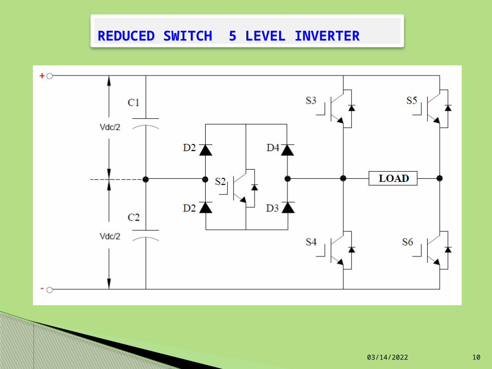
REDUCED SWITCH 5 LEVEL INVERTER
05/03/2023 10
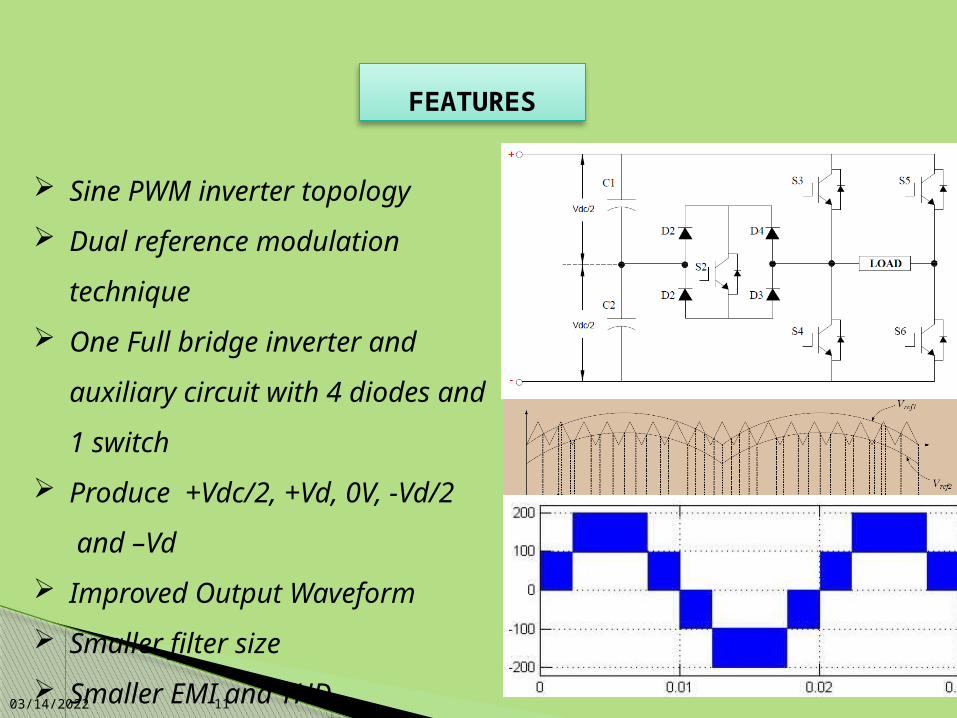
FEATURES
Sine PWM inverter topology Dual reference modulation
technique One Full bridge inverter and
auxiliary circuit with 4 diodes
and 1 switch Produce +Vdc/2, +Vd, 0V, -Vd/2
and –Vd
Improved Output Waveform Smaller filter size Smaller EMI and THD05/03/2023 11
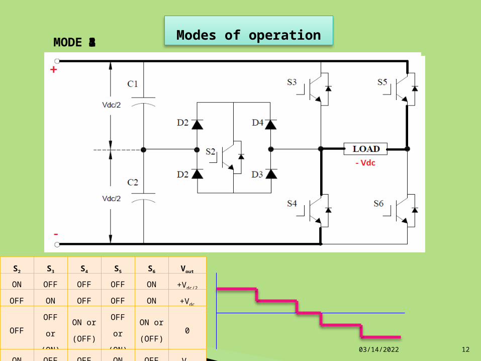
Modes of operation
S2 S3 S4 S5 S6 Vout
ON OFF OFF OFF ON +Vdc/2
OFF ON OFF OFF ON +Vdc
OFFOFF or (ON)
ON or (OFF)
OFF or (ON)
ON or (OFF)
0
ON OFF OFF ON OFF -Vdc/2
OFF OFF ON ON OFF -Vdc
MODE 21345
05/03/2023 12
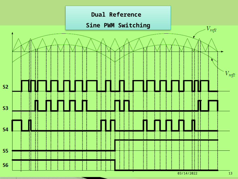
Dual Reference Sine PWM Switching
05/03/2023 13
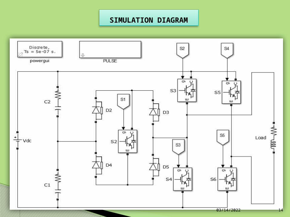
SIMULATION DIAGRAM
05/03/2023 14
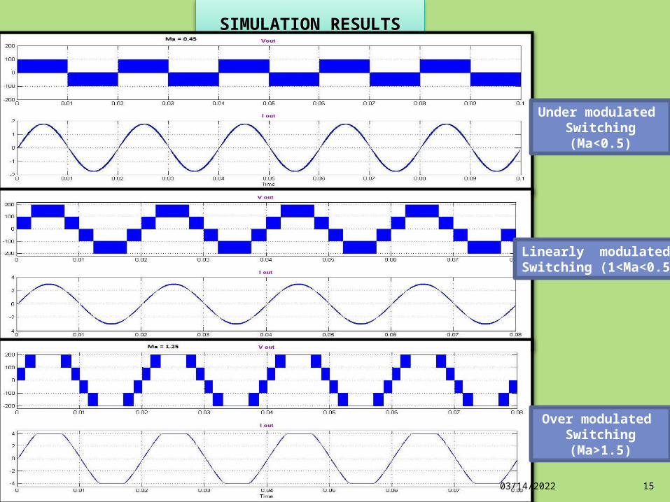
SIMULATION RESULTS
Under modulated Switching (Ma<0.5)
Linearly modulated Switching (1<Ma<0.5)
Over modulated Switching (Ma>1.5)
05/03/2023 15
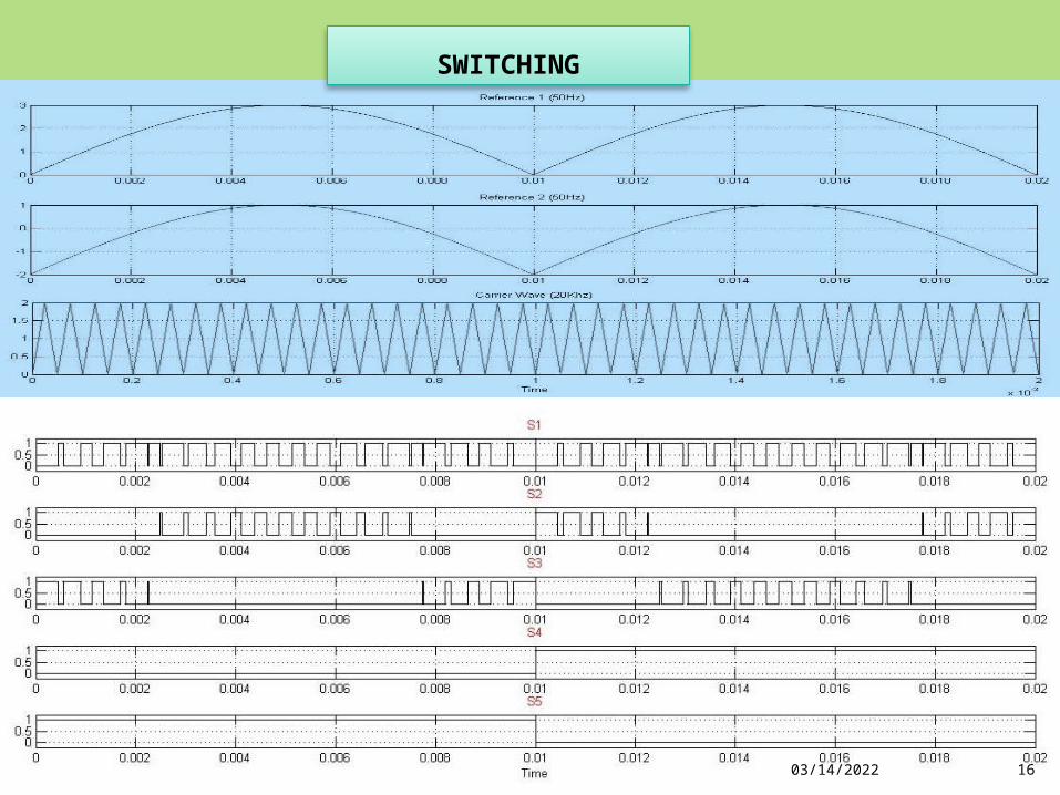
SWITCHING
05/03/2023 16
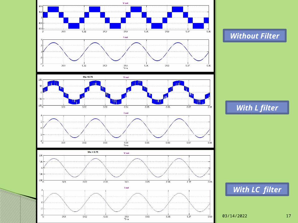
Without Filter
With L filter
With LC filter
05/03/2023 17
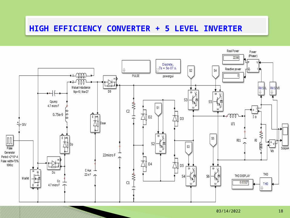
HIGH EFFICIENCY CONVERTER + 5 LEVEL INVERTER
05/03/2023 18
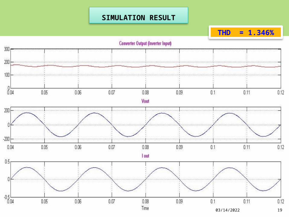
SIMULATION RESULT
05/03/2023 19
THD = 1.346%

ANALYSIS ON SIMULATION RESULTSSwitching Frequency
(Hz)
Duty Ratio
Load Vdc (Avg)
I in (Avg)Input power
V out (Avg)
I out (Avg)Pout
powerVoltage
Gain% µ
R
CONVERTER
16000 70%
1000 30 1.39 41.73 173.5 0.17 30.1 5.78 72%
600 30 1.54 45.43 146 0.24 35.55 4.87 78%500 30 1.60 47.81 138.6 0.28 38.36 4.62 80%400 30 1.74 52.17 131.2 0.33 43.04 4.37 82%250 30 2.50 74.74 127.8 0.51 65.31 4.26 87%200 30 3.04 91.18 127.6 0.64 81.42 4.25 89%100 30 5.75 172.7 126.5 1.26 160.1 4.22 93%
INVERTER
Hc =20 KHz & Href =
50Hz70%
1000 200 0.10 19.13 104.17 0.10 13.11 0.52 69%
500 200 0.19 37.81 120.8 0.24 25.19 0.60 67%300 200 0.29 57.83 121.4 0.40 42.12 0.61 73%200 200 0.40 79.34 118 0.59 64.54 0.59 81%
CONVERTER + INVERTER
70%
500 30 1.37 41.05 110.4 0.22 21.05 3.68 51%300 30 1.44 43.07 88.26 0.29 26.23 2.94 61%200 30 1.55 46.41 82.61 0.41 35.62 2.75 77%100 30 2.06 60.65 70.37 0.70 50.44 2.35 83%
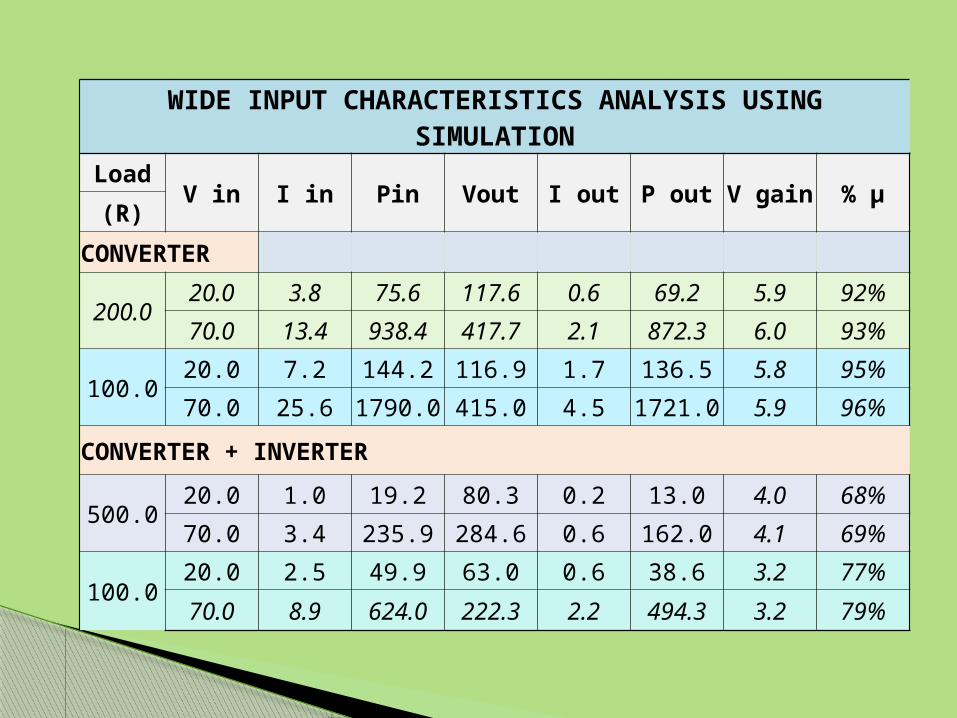
WIDE INPUT CHARACTERISTICS ANALYSIS USING SIMULATION
LoadV in I in Pin Vout I out P out V gain % µ
(R)CONVERTER
200.020.0 3.8 75.6 117.6 0.6 69.2 5.9 92%70.0 13.4 938.4 417.7 2.1 872.3 6.0 93%
100.0 20.0 7.2 144.2 116.9 1.7 136.5 5.8 95%70.0 25.6 1790.0 415.0 4.5 1721.0 5.9 96%
CONVERTER + INVERTER
500.0 20.0 1.0 19.2 80.3 0.2 13.0 4.0 68%70.0 3.4 235.9 284.6 0.6 162.0 4.1 69%
100.0 20.0 2.5 49.9 63.0 0.6 38.6 3.2 77%70.0 8.9 624.0 222.3 2.2 494.3 3.2 79%
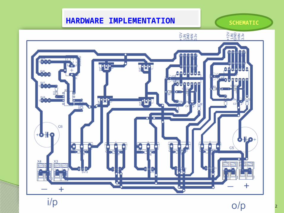
HARDWARE IMPLEMENTATION
05/03/2023 22
SCHEMATIC
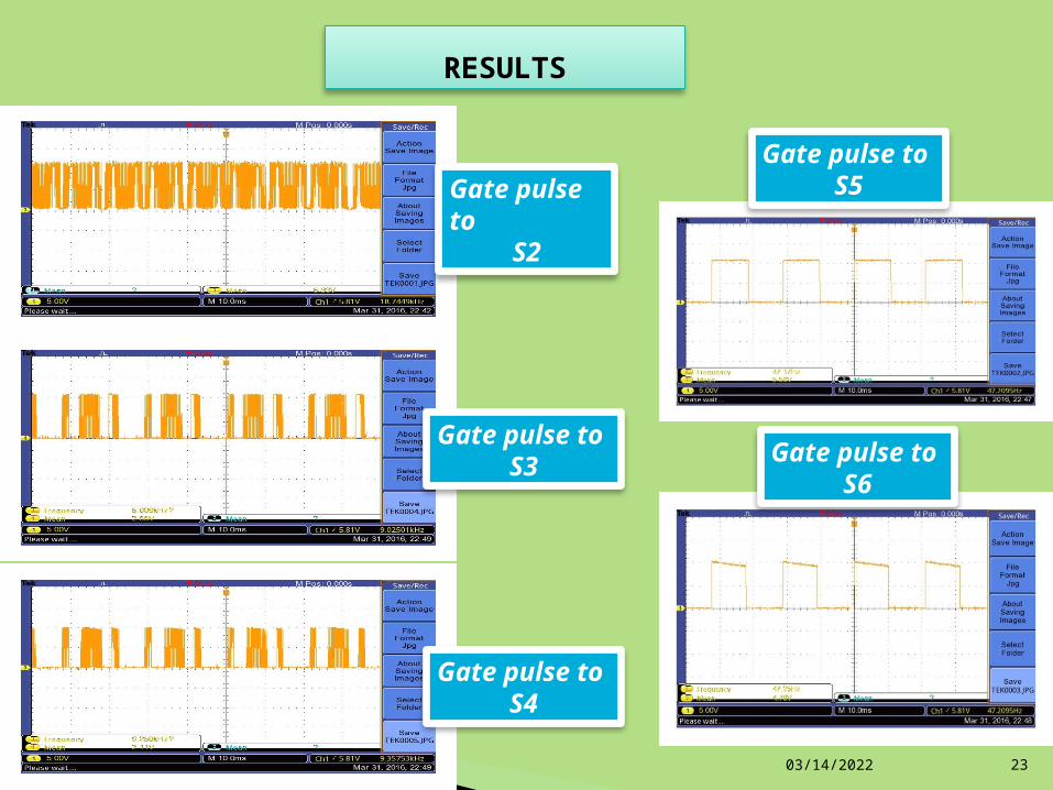
RESULTS
05/03/2023 23
Gate pulse to
S2
Gate pulse to S3
Gate pulse to S4
Gate pulse to S5
Gate pulse to S6
05/03/2023 24
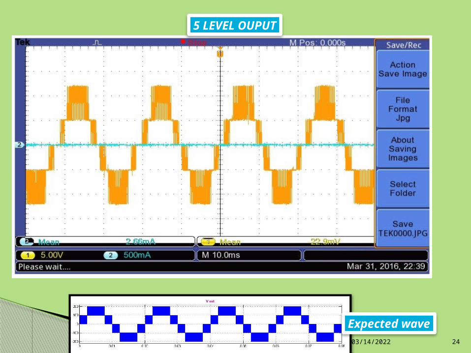
5 LEVEL OUPUT
Expected wave
CONCLUSION
Circuit Provides minimum THD (1.3% to 4.0% ) High Voltage gain about 2.5 to 10 times by keeping high
efficiency Providing wide input range characteristics The converter circuit recovers leakage inductance energy. The reduced switch multilevel inverter used 3 switches lesser
than conventional topology Switching losses comparatively lesser because of reduced
switches and two switches triggering with standard frequency The switching signals are generated with the help of
microcontroller dsPIC30F2010 Integration of converter with inverter provides high amplified
output with lesser THD and High efficiency about 80% and
above
Reference
1. TOMASZUK_ and A. KRUPA, “ High efficiency high step-up DC/DC converters – a review,” Bulleti of the polish
academy of sciences technical science, Vol. 59, No. 4, 2011
2. W. Yu, C. Hutchens, J.-S. Lai, J. Zhang, G. Lisi, A. Djabbari, G. Smith, and T. Hegarty, “High efficiency converter
with charge pump and coupled inductor for wide input photovoltaic AC module applications”, Energy Conversion
Congress and Exposition (ECCE) IEEE 1, 3895–3900 (2009).
3. S. J. Park, F. S. Kang, M. H. Lee, C. U. Kim, “A New Single-Phase Five-Level PWM Inverter Employing a
Deadbeat Control Scheme,” IEEE Trans. Power Electronics., vol. 18, no. 18, pp. 831-843, May. 2003.
4. Muhammad H. Rashid, Power electronics: Circuits, Devices, and Applications, 3rd ed. Pearson Prentice Hall, 2004,
pp.267.
5. Janyavula Deepthi and Dr S N Saxena, “Study of Variation of THD in a Diode Clamped Multilevel Inverter with
respect to Modulation Index” , 2nd International Conference and workshop on Emerging Trends in Technology
(ICWET) , International Journal of Computer Applications® (IJCA),2011
6. Paterrson Thomas, “Comparative study of three types of inverters basedon the output total harmonic distortion”,
2015, http://scholarsmine.mst.edu/masters_theses
7. Jean Noël Fiorina, “inverters and Harmonics”, Cahier Technique Merlin Gerin n° 159 / p.20, E/CT 159 first issued
september 1993
05/03/2023 26

Thank you for your attention . . .