High Dielectric Constant (k) Materialscoen.boisestate.edu/bknowlton/files/2011/09/MSE...High...
7
1 MSE 310/ECE 340 Electrical Properties of Materials 1 Knowlton Part 6: High Dielectric Constant (k), Gate Electrode, and Channel Materials ox EOT high k high k k t t k o ox ox ox k A C t Crystalline Si poly-crystalline Si amorphous SiO 2 Channel Si Wafer Insulator Insulator SiO 2 - Gate oxide Source Contact Drain Contact Poly Si Gate Contact source drain - - V gate V Drain channel + + + + + + + + + + + + + + M. Houssa et al., Materials Science and Engineering R, 51 (2006) 37-85 SiO 2 gate oxide is approaching physical limits thickness & current Frank, Dennard, Nowak, Soloman, Wong & Taur, Proceedings of the IEEE Circuit & Devices Device Scaling Limits, 89 (2001) 259 MSE 310/ECE 340 Electrical Properties of Materials 2 Knowlton High Dielectric Constant (k) Materials Robertson, J. Vac. Sci. Technol. B, 18(3), May/Jun 2000 Robertson, MRS Bulletin (March 2002) p. 217 Bandgap versus Dielectric Constant (k) Hik c Si Hik Si c e E e e e E Trend : As k ↑, E g ↓
Transcript of High Dielectric Constant (k) Materialscoen.boisestate.edu/bknowlton/files/2011/09/MSE...High...

1
MSE 310/ECE 340Electrical Propertiesof Materials
1Knowlton
Part 6: High Dielectric Constant (k), Gate Electrode, and Channel Materials
oxEOT high k
high k
kt t
k
o oxox
ox
k AC
t
Crystalline Si
poly-crystallineSi
amorphous SiO2
Channel
Si Wafer
Insulator InsulatorSiO2 - Gate oxide
Source Contact Drain ContactPoly SiGate Contact
source drain
-
-Vgate
VDrain
channel+ + ++ + + ++ + ++ + + +
M. Houssa et al., Materials Science and Engineering R, 51 (2006) 37-85
SiO2 gate oxide is approaching physical limitsthickness & current
Frank, Dennard, Nowak, Soloman, Wong & Taur, Proceedings of the IEEE Circuit & Devices Device Scaling Limits, 89 (2001) 259
MSE 310/ECE 340Electrical Propertiesof Materials
2Knowlton
High Dielectric Constant (k) Materials
Robertson, J. Vac. Sci. Technol. B, 18(3), May/Jun 2000Robertson, MRS Bulletin (March 2002) p. 217
Bandgap versus Dielectric Constant (k)
Hik c Si
Hik Si c
e E e
e e E
Trend: As k ↑, Eg ↓

2
MSE 310/ECE 340Electrical Propertiesof Materials
3Knowlton
High Dielectric Constant (k) Materials
Band Offsets: High k on Si
Robertson, MRS Bulletin (March 2002) p. 217
Hik c Si
Hik Si c
e E e
e e E
Aspects to Consider:1. Eg2. Ec & Ev3. meff
* 2
Recall in Barrier Region:
So:
2 ( )
,
kx
kx
eff e
eff
eff
e
J e
m V Ek
k m
m J
MSE 310/ECE 340Electrical Propertiesof Materials
4Knowlton
High Dielectric Constant (k) Materials
Band diagrams of MOS – compare SiO2 to high k materials
Southwick & Knowlton, IEEE TDMR, 6(2), (2006) 136-145

3
MSE 310/ECE 340Electrical Propertiesof Materials
5Knowlton
High Dielectric Constant (k) Materials
Need to consider the Thermodynamics of the materials system
Ellingham diagramG –vs- Temperature
The more negative Gis, the more stable the materials system is.
Example:
Grow Y2O3 on Si, Si will steal oxygen from Y2O3 to form interfacial layer (IL) of SiO2. Why?
R. DeHoff, Thermodynamics of Materials, (Prentice Hall, 1996) Ch. 11, fig. 11.4
SiO2
Y2O3
Al2O3
2 2 3
2 2 3 more stable than
SiO Y OG G
SiO Y O
MSE 310/ECE 340Electrical Propertiesof Materials
6Knowlton
High Dielectric Constant (k) MaterialsInterfacial layer (IL) of SiO2 Present for HfO2
, ,ox
ox eff ox physical high khigh k
kt t t
k
0 2 4 6 8 10 12 14tHfO2 nm
0
0.5
1
1.5
2
2.5
3
3.5
TOE
mn
EOT WRT tSiO2 & tHfO2
HfO2
CrystallineSi Channel
TiN
SiO2IL

4
MSE 310/ECE 340Electrical Propertiesof Materials
7Knowlton
High Dielectric Constant (k) Materials
EOT:
7 nm HfO2 & 1nm SiO2:EOT ~ 2 nm
8 nm HfO2: EOT ~ 1.25 nm
Southwick & Knowlton, IEEE TDMR, 6(2), (2006) 136-145
MSE 310/ECE 340Electrical Propertiesof Materials
8Knowlton 8
Possible Solution - SONOS
SONOS (SiO2-Si3N4-SiO2-Si) Advantages over Floating Gate:
Replace poly-Si floating gate with Si3N4
Stored charge lies in defect (bound) states below Si3N4 conduction bandImproved endurance - single defect will not cause the discharge/leakage of carriersCan reduce Thickness of TOSi3N4 thinner than floating gate Poly SiCarriers not “Floating” aroundMinimizes interaction with neighboring memory cellsThus, can scale down memory cell size
Todd Wallinger, SONOS Eases Non-Volatile Memory Integration in SoC, Semiconductor International (2007)
TLTL
BLBL
CTLCTL

5
MSE 310/ECE 340Electrical Propertiesof Materials
9Knowlton 9
Possible Solution - SONOS
Todd Wallinger, SONOS Eases Non-Volatile Memory Integration in SoC, Semiconductor International (2007)
PolySi
PolySi
Floating Gate Si
BL TL BL TL
Si3N4
Si
Gate stack scaled down in thickness & cell area
Energy BandDiagram
Energy BandDiagram
TLTL
BLBL
Flat BandCondition
CTLCTL
CTLCTL
= CTL= CTL
MSE 310/ECE 340Electrical Propertiesof Materials
10Knowlton 10
Possible Solution - SONOS
Todd Wallinger, SONOS Eases Non-Volatile Memory Integration in SoC, Semiconductor International (2007)
Poly Si
BL TL
Si3N4
Si
Gate stack scaled down in thickness & cell area
Energy BandDiagram
Flat BandCondition

6
MSE 310/ECE 340Electrical Propertiesof Materials
11Knowlton
High Dielectric Constant (k) Materials
Multilayer high k dielectric films for memory applications
Lee et al., Symposium on VLSI Technology Digest of Technical Papers (2006)Sanghun et al., IEEE TED 52 (2005) 2654.pdf
TANOS (Si/SiO2/SiN/A2O3/TaN)
SONOS (poly Si–SiO –SiN–SiO –Si)
MANOS (metal–Al2O3–SiN–SiO –Si)
MSE 310/ECE 340Electrical Propertiesof Materials
12Knowlton
Low Dielectric Constant (k) Materials
What About Low-k Dielectric Materials?
What would they be used for?
o oxox
ox
k AC
t
7
MSE 310/ECE 340Electrical Propertiesof Materials
13Knowlton
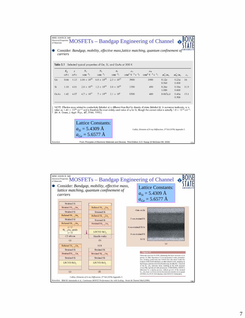
MOSFETs – Bandgap Engineering of Channel
Consider: Bandgap, mobility, effective mass,lattice matching, quantum confinement of carriers
From Principles of Electronic Materials and Devices, Third Edition, S.O. Kasap (© McGraw-Hill, 2005)
Lattice Constants:aSi = 5.4309 ÅaGe = 5.6577 Å
Cullity, Elements of X-ray Diffraction, 2nd Ed (1978) Appendix 5
MSE 310/ECE 340Electrical Propertiesof Materials
14Knowlton
MOSFETs – Bandgap Engineering of ChannelConsider: Bandgap, mobility, effective mass, lattice matching, quantum confinement of carriers
IBM RJ Antoniadis et al., Continuous MOFET Performance Inc with Scaling - Strain & Channel Matl (2006)
Lattice Constants:aSi = 5.4309 ÅaGe = 5.6577 Å
Cullity, Elements of X-ray Diffraction, 2nd Ed (1978) Appendix 5