
High-density data storage based on the atomic force microscope
14
High-Density Data Storage Based on the Atomic Force Microscope H. JONATHON MAMIN, ROBERT P. RIED, MEMBER, IEEE, BRUCE D. TERRIS, AND DANIEL RUGAR, MEMBER, IEEE Invited Paper The atomic force microscope (AFM), with its ability to image and modify surfaces on the nanometer scale, offers the potential for simple, compact, high-density data-storage devices. At the heart of the technique is a microfabricated cantilever with a sharp tip on the end. Using modern micromachining techniques, it is possible to batch fabricate cantilevers with tips that are sharp on the scale of 100 ˚ A. We have pursued a particular AFM storage scheme based on mechanical readback of topographic data using high- frequency, piezoresistive silicon cantilevers. Areal densities of 65 Gbit/in have been demonstrated, with readback rates greater than 10 Mbit/s. Nanoreplication techniques have been used to produce read-only disks. In addition, a write-once scheme was developed that uses integrated heating elements on the cantilevers in order to perform thermomechanical writing on a polymer substrate. Considerable progress has been made in addressing critical issues such as data rate, reliability, and practical implementation, but significant challenges still remain, both in the technology and in finding the most suitable applications. Keywords— Atomic force microscope, memories, microelectro- mechanical devices, piezoresistive devices. I. INTRODUCTION The history of the information age has been characterized by rapid advances in the underlying component technolo- gies, leading to continuous improvements in computing power at ever-decreasing cost. Much of the benefit has arisen from the power of scaling, as exemplified by the well-known Moore’s Law. In mass data storage based on magnetic recording, the progress has been just as dramatic as in semiconductor devices. In the past 40 years, the areal density of disk drives has increased by six orders of magnitude [1]. Recent laboratory demonstrations made at an areal density of 12 Gbit/in suggest that progress will continue for some time [2]. History is, in fact, littered Manuscript received November 19, 1998; revised February 16, 1999. This work was supported in part by DARPA Contract DABT-63-95-C- 0019. H. J. Mamin, B. D. Terris, and D. Rugar are with the IBM Research Division, Almaden Research Center, San Jose, CA 95120-6099 USA. R. P. Ried is with Input/Output, Inc., Stafford, TX 77477-2409 USA. Publisher Item Identifier S 0018-9219(99)04046-3. with failed predictions of the demise of magnetic recording. Still, one can be fairly certain that densities for magnetic recording will not increase another six orders of magnitude, as this would require bit cells of atomic dimensions. Indeed, at densities in the range of 100 Gbit/in (which are less than ten years away at the current rate of progress [1]), superparamagnetic effects, in which the magnetic bits are no longer stable at room temperature, are expected to pose serious challenges. It is therefore prudent to make some examination of technologies that could have the potential to provide a pathway to the higher densities needed in the years ahead. Ever since the invention of the scanning tunneling mi- croscope (STM) [3], with its ability to image surfaces at the atomic scale, people have envisioned the possibility of applying the technique to perform ultrahigh-density data storage [4]. A wide variety of schemes have been demonstrated for using the STM and its offspring, the atomic force microscope (AFM) [5], to modify as well as image surfaces with spatial resolution ranging from angstroms to tens of nanometers [6], [7]. Much of the work has focused on fundamental understanding of the mechanisms and interactions between the tip and sample. In the case of AFM-based storage, work toward a tip- based data-storage system has progressed beyond simply demonstrating the ability to make a small mark. Research is underway to address such critical issues as data rate, error rates, tracking, integration, and reliability. It is this work that is the main subject of this paper. II. GENERAL CONSIDERATIONS FOR SCANNING PROBE DATA STORAGE A. STM-Based Data Storage In the STM, a sharp tip is scanned in close proximity to a surface. An applied voltage between the tip and sample gives rise to a tunnel current that depends sensitively on the tip-sample separation. As the tip is scanned, the 0018–9219/99$10.00 1999 IEEE 1014 PROCEEDINGS OF THE IEEE, VOL. 87, NO. 6, JUNE 1999
Transcript of High-density data storage based on the atomic force microscope

High-Density Data Storage Based onthe Atomic Force Microscope
H. JONATHON MAMIN, ROBERT P. RIED,MEMBER, IEEE,
BRUCE D. TERRIS,AND DANIEL RUGAR, MEMBER, IEEE
Invited Paper
The atomic force microscope (AFM), with its ability to imageand modify surfaces on the nanometer scale, offers the potential forsimple, compact, high-density data-storage devices. At the heart ofthe technique is a microfabricated cantilever with a sharp tip onthe end. Using modern micromachining techniques, it is possibleto batch fabricate cantilevers with tips that are sharp on the scaleof 100 A. We have pursued a particular AFM storage schemebased on mechanical readback of topographic data using high-frequency, piezoresistive silicon cantilevers. Areal densities of 65Gbit/in2 have been demonstrated, with readback rates greater than10 Mbit/s. Nanoreplication techniques have been used to produceread-only disks. In addition, a write-once scheme was developedthat uses integrated heating elements on the cantilevers in orderto perform thermomechanical writing on a polymer substrate.Considerable progress has been made in addressing critical issuessuch as data rate, reliability, and practical implementation, butsignificant challenges still remain, both in the technology and infinding the most suitable applications.
Keywords—Atomic force microscope, memories, microelectro-mechanical devices, piezoresistive devices.
I. INTRODUCTION
The history of the information age has been characterizedby rapid advances in the underlying component technolo-gies, leading to continuous improvements in computingpower at ever-decreasing cost. Much of the benefit hasarisen from the power of scaling, as exemplified by thewell-known Moore’s Law. In mass data storage based onmagnetic recording, the progress has been just as dramaticas in semiconductor devices. In the past 40 years, theareal density of disk drives has increased by six ordersof magnitude [1]. Recent laboratory demonstrations madeat an areal density of 12 Gbit/insuggest that progresswill continue for some time [2]. History is, in fact, littered
Manuscript received November 19, 1998; revised February 16, 1999.This work was supported in part by DARPA Contract DABT-63-95-C-0019.
H. J. Mamin, B. D. Terris, and D. Rugar are with the IBM ResearchDivision, Almaden Research Center, San Jose, CA 95120-6099 USA.
R. P. Ried is with Input/Output, Inc., Stafford, TX 77477-2409 USA.Publisher Item Identifier S 0018-9219(99)04046-3.
with failed predictions of the demise of magnetic recording.Still, one can be fairly certain that densities for magneticrecording will not increase another six orders of magnitude,as this would require bit cells of atomic dimensions. Indeed,at densities in the range of 100 Gbit/in(which are lessthan ten years away at the current rate of progress [1]),superparamagnetic effects, in which the magnetic bits areno longer stable at room temperature, are expected to poseserious challenges. It is therefore prudent to make someexamination of technologies that could have the potentialto provide a pathway to the higher densities needed in theyears ahead.
Ever since the invention of the scanning tunneling mi-croscope (STM) [3], with its ability to image surfaces atthe atomic scale, people have envisioned the possibilityof applying the technique to perform ultrahigh-densitydata storage [4]. A wide variety of schemes have beendemonstrated for using the STM and its offspring, theatomic force microscope (AFM) [5], to modify as wellas image surfaces with spatial resolution ranging fromangstroms to tens of nanometers [6], [7]. Much of thework has focused on fundamental understanding of themechanisms and interactions between the tip and sample.In the case of AFM-based storage, work toward a tip-based data-storage system has progressed beyond simplydemonstrating the ability to make a small mark. Researchis underway to address such critical issues as data rate,error rates, tracking, integration, and reliability. It is thiswork that is the main subject of this paper.
II. GENERAL CONSIDERATIONS FOR
SCANNING PROBE DATA STORAGE
A. STM-Based Data Storage
In the STM, a sharp tip is scanned in close proximity toa surface. An applied voltage between the tip and samplegives rise to a tunnel current that depends sensitivelyon the tip-sample separation. As the tip is scanned, the
0018–9219/99$10.00 1999 IEEE
1014 PROCEEDINGS OF THE IEEE, VOL. 87, NO. 6, JUNE 1999

Fig. 1. Atomic-scale message demonstrating the ability to position single atoms with angstomprecision. Each bump is an individual xenon atom positioned with the tip of a scanning tunnelingmicroscope operating at 4.2K. This represents perhaps the ultimate in data-storage density, with asingle atomic “bit” (courtesy of D. Eigler, IBM Research Division, Almaden Research Center).
tunnel current is monitored and the tip position is servoedto maintain constant current. In this way, the underlyingsurface topography is mapped out [3]. From a data-storageperspective, the chief advantage of this approach, andperhaps the only reason it is worth contemplating, is thatone can truly image and modify surfaces with the tip ona nanometer, or even atomic, scale. A famous example ofthis is shown in Fig. 1, where individual xenon atoms werepositioned with angstrom precision using an STM to spellout “IBM.” This seminal work by Eigler and Schweizer wasperformed in ultrahigh vacuum (UHV) at 4.2K, and tookabout 22 h [8]. Though not performed for the purposes ofdata storage, this demonstration represents an effective arealdensity of the order of 10 bits/in , or 1 million Gbit/in(1.6 10 bit/cm ).
The STM has some characteristics, however, that wouldtend to seriously limit the speed and reliability of an STM-based storage device. Because of the steep dependence ofthe tunnel current on separation, the tip-sample separationmust be maintained to within about 0.1A to achievereasonable current stability. Using an active servo to dothis with any reasonable speed is difficult. There has beensome progress in improving the bandwidth of the STMusing novel mechanics and servo schemes [9], but suchimprovements have not come easily. The possibility ofoperating without a servo has often been proposed, butsuitable samples that have the required degree of flatnessover large scales have yet to be demonstrated.
In addition, the STM suffers from the difficulty of itsextreme dependence on the surface properties (e.g., work-function, oxidation state, cleanliness, etc.), and the exactconfiguration of the tip. These effects give rise to largeand unpredictable changes in tunnel current, especiallywhen operating under less than UHV conditions. For thesereasons, much of the work in data-storage applications hasfocused on the atomic force microscope implementation.
B. AFM-Based Data Storage
In the AFM, the sharp tip sits on the end of a softcantilever spring, so that extremely small forces are capable
Fig. 2. Image obtained with the AFM showing individual siliconadatoms on a clean reconstructed Si (111) surface (courtesy of R.Erlandsson, Linkoping University, Sweden).
of being sensed and applied [5]. The advantage is that thetip can actually “touch” the surface, i.e., come into repulsivecontact with it, without necessarily destroying the tip orsurface, due to the compliance of the cantilever. The tip canalso operate in a noncontact mode, in which it responds tothe attractive or repulsive forces exerted on it by the surface.
As with the STM, the AFM is capable of true atomicresolution. An example is shown in Fig. 2, in which in-dividual silicon adatoms in the famous Si (7 7) surfacereconstruction have been imaged on a clean surface in UHVusing noncontact mode AFM [10]. This remarkable abilityto access the atomic scale is what makes AFM-based datastorage so enticing.
Though the AFM holds the potential for atomic-levelstorage, any practical implementation of such a scheme isstill far from reality. As in STM, a major obstacle is theneed to move the tip at high speeds over a surface while
MAMIN et al.: HIGH-DENSITY DATA STORAGE 1015

Fig. 3. Concept of topographic data storage using an AFM tip.The tip rides over the surface of the substrate, causing deflectionof the cantilever as the tip moves over a topographic feature. Thedeflection is detected via a piezoresistive sensor.
controlling the tip-sample separation at the angstrom level.One can alternatively operate with the tip in contact, assuggested in Fig. 3. The advantage here is that, insteadof trying to maintain the tip at a fixed height above therapidly moving surface, following every hill and valley,the tip automatically follows the surface topography dueto the compliance of the cantilever. (Of course the varyingtopography will affect the loading force, so that the fea-ture heights must be kept below a reasonable limit.) Byeliminating the need for an active servo, the potential forhigh data rate is increased. The tradeoff is that one hasto deal with the tribology issues of sliding contact andits implications for reliability. Also, even at low loadingforces, the peak stresses can be quite high if the tip is verysharp. The result is that the bit sizes achieved in contactmode tend to be far from the atomic scale. Nonetheless,the densities are still high enough to be of considerableinterest, and contact-mode remains the basis for the mosthighly developed AFM storage approaches.
In the end, the chief advantage of the AFM approachto data storage may rest in its simplicity. Compared to amagnetic recording head, the tip is a very simple structure.It is reasonably straightforward, using conventional lithog-raphy and modern micromachining techniques to make tipsthat are sharp on the 100A scale, if not the atomic scale.Indeed, the entire concept of AFM storage is in principlenot very complicated: one has the media, a tip with sometype of sensor, and the means to move one relative to theother. The technique could potentially be simple, compact,and inexpensive.
C. Nontopographic Schemes for Probe-Based Data Storage
The tip of the AFM can respond not only to topographicchanges in the surface, but also to nontopographical ones,such as electrical or optical properties. An exhaustivereview of AFM data storage efforts is beyond the scopeof this paper. However, some examples of nontopographicapproaches are described below to illustrate the range ofpossibilities. In most cases, the AFM cantilever is usedprimarily as a convenient way to allow tip-sample contactat low loading forces.
One promising scheme based on charge storage in nitride-oxide-semiconductor (NOS) structures has been demon-
strated by Barrett and Quate [11]. The principle is similarto a flash memory, using the tip as a moving electrode.A voltage pulse on the tip causes charge to tunnel froma silicon substrate through an oxide barrier into a nitridefilm, where it is trapped. This causes a depletion regionthat can be detected as a change in capacitance. Usinga conducting AFM tip operating in contact, Barrett andQuate were able to show highly reliable writing with marksas small as 700A. The technique has the advantage thatit is electrical, so it is not limited by mechanical datarates. Though not strictly rewritable in the usual sense, itis reversible, with submillisecond erase times and up to10 read–write cycles expected [11], [12]. It is also notstrictly necessary to operate in contact, though the loss ofsignal is precipitous as one introduces an air gap, due tothe low dielectric constant of air. It remains to be seenwhether signal-to-noise issues and media issues will permithigher densities. A more immediate difficulty encounteredby Terris and Barrett is that of tip wear [13]. The nitridelayer is very hard, and it is very effective at blunting thetip, especially as one goes toward reasonably high velocitybetween tip and sample. It may be that with advancesin conducting diamond tips or carbon nanotube tips [14],this problem could be ameliorated. Depending on what theultimate density limits of this technique turn out to be, thistechnique could merit more attention.
Another electrical approach, demonstrated by Kado andTohda [15], uses a conducting tip to inject current intoa chalcogenide film similar to that used in optical phase-change recording [16]. The medium heats up or otherwiseis affected by the high current density or field and changesfrom an amorphous phase to a crystalline phase. As a resultof the phase transformation, the properties of the mediumchange, in particular its resistivity. The marks are thenread by measuring resistance between tip and substrateas the tip is scanned over the marks. In an impressivedemonstration, marks on the order of 100A were writtenand read back in this way. The technique requires a robustconducting tip and a relatively low tip-sample resistance,requirements that can be challenging when there is slidingcontact [17]. Again, advances in conducting diamond tipsor other coating technologies could alleviate this problem.
Nontopographic approaches based on near-field opticaltechniques have also been explored. The use of near-field scanning optical microscopy (NSOM) has beendemonstrated by Betziget al. to perform reading andwriting in magneto-optic materials [18]. In order to getaround the problem of low photon flux through the near-field apertures in traditional NSOM, Zenhausern, Martin,and Wickramasinghe have developed an aperturelesstechnique dubbed SIAM for scanning intereferometricapertureless microscopy [19]. In this approach, a tip is usedin place of an aperture. The tip acts as a localized scattererof light, with its scattering properties modulated by thedipole–dipole interaction with the sample. A heterodynedetection scheme, in which the scattered light interfereswith a reference beam, is used to increase the photonflux at the detector. Imaging on the 10-A scale has been
1016 PROCEEDINGS OF THE IEEE, VOL. 87, NO. 6, JUNE 1999

demonstrated with this technique, and Martinet al. haveused the approach to read out compact-disk-like patternswith a minimum feature size of 500A [20]. An analysisof the signal-to-noise ratio suggests that data rates of 30MHz or higher might be achievable. This approach has theadvantage that it does not require contact between the tipand sample, though in that case, some means must be foundto keep them in close proximity at high relative speeds.
One way to address this last issue is by adopting thetype of air-bearing technology used in magnetic recording.This approach has been used to perform a type of near-field optical recording using a special type of lens knownas a solid immersion lens (SIL). The SIL is made of a highindex material, which allows for a smaller focused spotwithin the lens [21]. By flying the lens close to the media,bits that are smaller than the optical diffraction limit havebeen written and read [22].
III. AFM D ATA STORAGE WITH TOPOGRAPHICREADBACK
In the remainder of the paper, we will discuss in somedetail one particular approach to AFM data storage, focus-ing on the work done in our own laboratory. The approachis that of mechanical readback of topographic featureson a rotating disk with contact-mode AFM. We describethe advances in cantilever development to create high-frequency cantilevers with integrated piezoresistive sensorsthat allow high readback rates and compact implementation.A writing scheme based on heating of the tip is described, aswell as an alternative means for stamping read-only diskswith sub-1000A features. We also discuss some of thecritical systems issues. In particular, we show that trackingon data on 1000A wide tracks is possible. We discuss thereliability issue and show that for the favorable combinationof a soft media and a hard tip, extended operation withoutany media wear is possible. Finally, we discuss some of thechallenges, technical and otherwise, on the road ahead.
The basic concept of this scheme is shown in Fig. 3.A disk containing topographic features rotates under thetip. As the features move under the tip, the tip rides downinto the pit, causing deflection of the cantilever, which isdetected by some sort of sensor. This very simple conceptdid not originate with the AFM: it hearkens back to theoriginal phonograph. Other stylus-based schemes have alsobeen developed, such as the RCA video disk [23]. Whatdistinguishes the AFM approach in this case is the abilityto microfabricate the very sharp tips and operate at verylow forces, so that one can achieve very high density andhigh data rate.
A. Cantilevers
Clearly the cantilever and the sensor structures are at theheart of the technique. Making suitable micromechanicalstructures has been a major part of the effort in ourlaboratory. What makes these components a challenge isthat they have to satisfy many conditions simultaneously.They must have high resonant frequency, because in thisscheme the data rate is determined by the mechanical
Fig. 4. Scanning electron micrograph of a 0.34�m thick, 12�m long, high-frequency single-crystal silicon cantilever with anintegrated piezoresistive sensor. The resonant frequency of thisdevice is 2.4 MHz.
response time. (Another way to achieve high data rates, byhaving multiple tips operating in parallel, will be describedlater.) High resonant frequency can be achieved by makingthe cantilevers stiff, but that is unacceptable, because lowloading forces are required to prevent damage to the tip ormedia. The way to achieve both high resonant frequency,and low stiffness , is to make the moving mass small,as can be seen by the simple harmonic oscillator relation
. Thus, the cantilevers should be thin, narrow,and short. There must of course be a sharp tip on the end.Finally, there must be a way to sense the motion of thecantilever, and the sensitivity must be adequate to detectthe small deflections in the bandwidth of interest.
The deflection sensor should ideally be integrated intothe cantilever. Tortoneseet al. have demonstrated the useof piezoresistive silicon cantilevers as integrated sensors[24]. We have taken this approach and further developed itto achieve high-frequency cantilevers.
Fig. 4 shows a scanning electron micrograph of one typeof single-crystal silicon piezoresistive cantilever that wehave developed [25]. It has a stiffness of about 1 N/m,a resonant frequency of 2.4 MHz, a length of 12m,and a thickness of 0.34m. An aluminum contact pad isused for injecting the current into the silicon cantilever,where it flows through a U-shaped silicon path and backto the other pad. The cantilever is made from a silicon-on-insulator (SOI) wafer and requires some novel processingsteps. Typically, AFM cantilevers are made through a bulkrelease process in which the entire wafer thickness is etchedaway from the back. This allows the cantilevers to overhangthe support, but it gives very poor control on the final lengthof the freestanding cantilever. For our short cantilevers, weneeded to develop an alternative. The cantilever shown herewas made with a front side release process, which givesexcellent control on the length. One alternative that hasrecently been demonstrated is to do a backside release witha deep reactive ion etch through the thickness of the wafer,which also gives excellent control [26].
MAMIN et al.: HIGH-DENSITY DATA STORAGE 1017

Incorporating piezoresistive sensors into such thin can-tilevers is a significant challenge, since the current must beconfined to one side of the neutral plane of the cantilever.Otherwise, the piezoresitive response due to the compres-sive stress on one side cancels the response due to thetensile stress on the other. To achieve this in our 0.34mthick cantilever, we used a low-energy implant followedby a rapid thermal anneal [25], [27]. Further details of thefabrication process can be found in [25].
The above cantilever also used a novel type of in-planetip. In this case, the tip sticks out like a spear fromthe cantilever. To access the surface of a sample withthe in-plane tip, the entire support chip and cantileverare angled at a fairly steep attack angle, 30–45.1 Theadvantage of the in-plane tip is that it adds essentiallyno mass to the cantilever and is very compatible withthin levers. In contrast, the mass of a more traditional tipcan load down the cantilever considerably and reduce itsresonant frequency, especially if one goes to even smallercantilevers. Also, the more traditional out-of-plane tips aremade through a subtractive process, so that one starts with asilicon layer as thick as the tip is high [24]. To end up witha thin lever, one needs extremely good tolerances to achievethe desired thickness. With the in-plane tip, the initial andfinal thicknesses of the silicon layer are the same, givingvery good thickness control.
The in-plane tip is formed by the intersection of threeplanes. One plane of the tip is that of the cantilever, oneis a plane perpendicular to the cantilever defined througha dry etch, and the third is a111 crystallographic planedefined in an anisotropic wet etch. Because the etch stopspreferentially on 111 planes, the process is very robust,and good tip uniformity can be achieved over the wafer.As evident in the scanning electron micrograph in Fig. 5,the tips can have a radius of curvature down to 40A.
The piezoresistive sensor on the cantilever has a dis-placement resolution down to 10 A/Hz , as shown inthe noise spectrum in Fig. 6. The baseline noise is closeto the intrinsic Johnson noise of the piezoresistor. Theintegrated noise in a 3-MHz bandwidth would be about 2A.In actuality, the integrated noise is typically higher (4–6A),because of excess noise. However, for features that are200A high, the minimum feature height of our samples, theratio of signal to sensor noise is at least 30 dB in a 3-MHzbandwidth, which is more than adequate. Fig. 6 shows anoise peak at 3 MHz, which is the resonant frequency ofour cantilever. This peak is due to the thermal-mechanicalmotion of the cantilever. It is insignificant for the data-storage application, as the integrated noise is negligible,but it does represent the first time to our knowledge that apiezoresistive cantilever has been sensitive enough to detectits own thermal noise in air.
1One should note that the effective stiffness of the cantilever changeswith the attack angle of the cantilever. If the cantilever is at an angle�with respect to the horizontal axis, then an analysis of the forces revealsthat the effective spring constant@Fz=@z = k0= cos2 �, wherez is thevertical axis, andk0 is the spring constant as usually defined.
Fig. 5. Scanning electron micrograph showing a close up of thein-plane tip. The radius is estimated to be 40A.
Fig. 6. Noise spectral density of the piezoresistive cantilevershowing its displacement resolution. The baseline noise of 1.3� 10�3 A/Hz1=2 is due to the Johnson noise of the resistor.The thermal-mechanical motion of the cantilever at its resonantfrequency of 3 MHz is clearly visible.
We have made even higher frequency piezoresistivecantilevers than described above. One example is shownin Fig. 7; it is 12 m long and has a 4.6-MHz resonantfrequency. We have also made an 8m long version witha 9-MHz resonant frequency. These should support datarates of at least 10 Mbit/s, as discussed below.
B. Write-Once and Read-Only Schemes
The above cantilevers are made for mechanical readbackof topographic information. The problem remains of how towrite the data on the disk. One scheme that we have pursuedfor some time is that of thermomechanical writing [28]. Inthis technique, the medium is a polymeric material suchas polycarbonate or polymethyl methacrylate (PMMA) ineither bulk or thin-film [29] form. The tip is heated by somemeans, causing heating and softening of the medium wherethe tip is in contact with it. The local pressure from the tipthen creates an indentation. In the original implementation[28], the tip heating was done via an external laser focusedon the tip. With this approach, it was possible to achieve
1018 PROCEEDINGS OF THE IEEE, VOL. 87, NO. 6, JUNE 1999
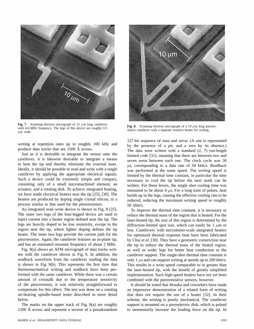
Fig. 7. Scanning electron micrograph of 12�m long cantileverwith 4.6-MHz frequency. The legs of this device are roughly 0.5�m wide.
writing at repetition rates up to roughly 100 kHz andproduce data tracks that are 1500A across.
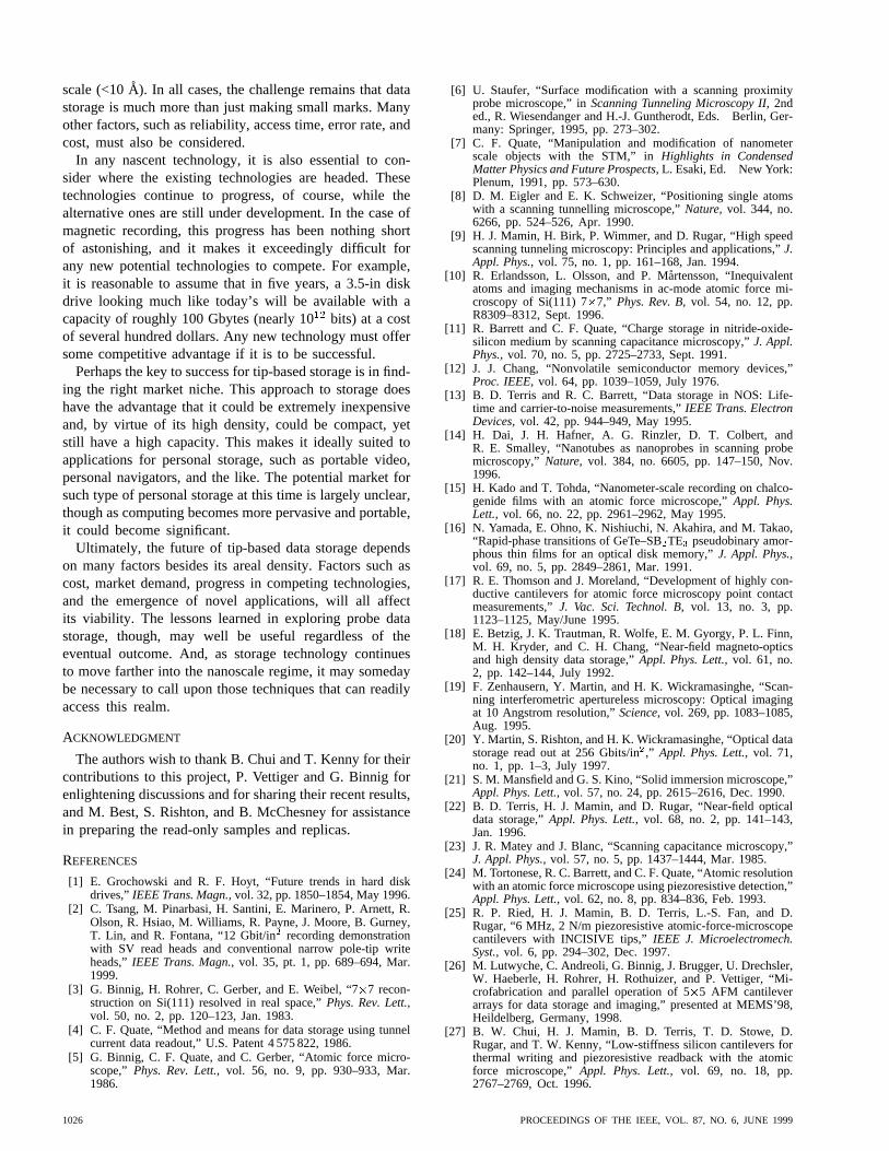
Just as it is desirable to integrate the sensor onto thecantilever, it is likewise desirable to integrate a meansto heat the tip and thereby eliminate the external laser.Ideally, it should be possible to read and write with a singlecantilever by applying the appropriate electrical signals.Such a device could be extremely simple and compact,consisting only of a small micromachined element, anactuator, and a rotating disk. To achieve integrated heating,we have made electrical heaters near the tip [25], [30]. Theheaters are produced by doping single crystal silicon, in aprocess similar to that used for the piezoresistors.
An integrated read–write device is shown in Fig. 8 [25].The outer two legs of the four-legged device are used toinject current into a heater region defined near the tip. Thelegs are heavily doped to be low resistivity, except in theregion near the tip, where lighter doping defines the tipheater. The inner two legs provide the current path for thepiezoresistor. Again, the cantilever features an in-plane tip,and has an estimated resonant frequency of about 2 MHz.
Fig. 9(a) shows an AFM micrograph of data tracks writ-ten with the cantilever shown in Fig. 8. In addition, thereadback waveform from the cantilever reading the datais shown in Fig. 9(b). This represents the first time thatthermomechanical writing and readback have been per-formed with the same cantilever. While there was a certainamount of crosstalk due to the temperature sensitivityof the piezoresistor, it was relatively straightforward tocompensate for this effect. The test was done on a rotatingair-bearing spindle-based tester described in more detailbelow.
The marks on the upper track of Fig. 9(a) are roughly1200 A across and represent a section of a pseudorandom
Fig. 8. Scanning electron micrograph of a 19�m long piezore-sistive cantilever with a separate resistive heater for writing.
127-bit sequence of ones and zeros. (A one is representedby the presence of a pit, and a zero by its absence.)The data were written with a standard (2, 7) run-lengthlimited code [31], meaning that there are between two andseven zeros between each one. The clock cycle was 30
s, corresponding to a data rate of 50 kbit/s. Readbackwas performed at the same speed. The writing speed islimited by the thermal time constant, in particular the timenecessary to cool the tip before the next mark can bewritten. For these levers, the single shot cooling time wasmeasured to be about 4s. For a long train of pulses, heatbuilds up in the legs, causing the effective cooling rate to bereduced, reducing the maximum writing speed to roughly50 kbit/s.
To improve the thermal time constant, it is necessary toreduce the thermal mass of the region that is heated. For thelaser-heated tip, the size of this region is determined by thediffraction-limited spot size, which can easily be 1m orless. Cantilevers with micrometer-scale integrated heatersfor optimized thermal response time have been fabricatedby Chuiet al. [30]. They have a geometric constriction nearthe tip to reduce the thermal mass of the heated region,as well as wider legs for better heat conduction to thecantilever support. The single-shot thermal time constant isonly 1 s and can support writing at speeds up to 200 kbit/s.This results in a write speed comparable to or greater thanthe laser-heated tip, with the benefit of greatly simplifiedimplementation. Such high-speed heaters have not yet beencombined with the piezoresistive sensors, however.
It should be noted that Hosaka and coworkers have madean impressive demonstration of a related form of writingthat does not require the use of a heater [32]. In theirscheme, the writing is purely mechanical. The cantileversupport is mounted on a piezoelectric disk, which is pulsedto momentarily increase the loading force on the tip. In
MAMIN et al.: HIGH-DENSITY DATA STORAGE 1019

(a)
(b)
Fig. 9. (a) Atomic force micrograph of data tracks composed of200 A high marks written thermomechanically with the integratedread–write device shown in Fig. 10. The scale bar is 1�m and (b)output waveform from the same device, reading at the same rate(50 kbit/s). Inset shows a portion of the rate 1/2 (2, 7) coding.
this way, the increased loading force causes a small pitto be made in the polycarbonate. Marks as small as 200Aacross have been written in this way, leading to a density of1 Tbit/in , among the highest of the AFM-based schemes.The marks have been read back on a rotating disk at speedsup to 1 MHz using low-mass cantilevers with an opticaldeflection sensor. The writing currently is slow, requiring5-ms pulses, but that is almost certainly not the intrinsiclimit.
Such topographic writing, whether thermally assisted ornot, is a write-once technique, though bulk erasing may wellbe possible. (For example, surface smoothing using heatinghas recently been demonstrated [33].) For many applica-tions, a write-once or read-only scheme may be adequate.In particular, the success of CD-ROM technology, forexample, shows that there is a large market for inexpensive,read-only data storage. While higher density versions ofCD-ROM, namely digital versatile disk (DVD)-ROM, arenow available, the growth path is limited by the laws ofoptics and the wavelength of light. Tip-based techniquesoffer one means to extend the concept of readback ofreplicated topographic disks to even higher densities. One
(a) (b)
Fig. 10. AFM images of (a) the e-beam written master and (b)the replica of features written on a track pitch of 1000A.
key factor is whether the features can be fabricated andreliably replicated at the nanometer scale.
Numerous approaches to replication of small featureshave been demonstrated recently, such as imprint lithog-raphy by Chouet al. [34] and pattern transfer of self-assembled monolayers by the Whitesides group [35]. Forour application, we have used an approach based on aphotopolymer technique [36]. First, a master disk wasproduced with the necessary small data features usingconventional electron-beam lithography. The substrate wasa silicon wafer with a layer of silicon oxide on top. Thepattern was written directly into a PMMA resist, and thena reactive ion etch was used to transfer the pattern intothe silicon oxide. A thin layer of amorphous TbFeCo wasthen sputtered onto the substrate to form a release layer.A small amount of the liquid photopolymer consisting ofa low-viscosity acrylate was placed on the master. A thintransparent substrate, typically a glass coupon, was then laidover the drop, causing it to flow over the area of the master.UV light was applied to cross link the photopolymer,turning it into a solid, hard layer. The glass substrate wasthen separated from the master, leaving the polymer replicabonded to the glass. The master could then be reused formaking another replica.
It was immediately evident that the replication processdoes an excellent job of reproducing the topography of themaster, even for feature sizes below 500A. Fig. 10 showsAFM micrographs of the master and the replica, showingexcellent fidelity of the pits, which have 500-A minimumdimension. The rms roughness of the replica is only 2–5A, comparable to the master. It is also possible to makereplicas of replicas in order to get back to the pit geometryand get a more direct comparison. The effective arealdensity in Fig. 10 is 65 Gb/in. Based on what we haveseen, we believe that it is possible to replicate even smallerfeatures and increase the density by another factor of four orso. Indeed, Krauss and Chou have recently demonstrated aform of imprint lithography capable of transferring patternsat densities up to 400 Gbit/in[37].
C. System Setup
The basic cantilever technology and writing/replicationmeans have been described above. In order to investigate
1020 PROCEEDINGS OF THE IEEE, VOL. 87, NO. 6, JUNE 1999

(a) (b)
Fig. 11. (a) Output waveform from the 4.6-MHz device of Fig. 7 in response to 1100-A highfeatures moving at 1 m/s on a spinning disk and (b) blow up of one section of the waveformshowing a 90 ns mechanical response.
real systems issues, such as data rate, error rate, timingjitter, track servoing, and long-term reliability, we haveoperated the cantilevers on a test stand capable of movingthe media at high speeds under the tip. The tester is builtaround an air-bearing spindle that provides sample rotation.One advantage of rotary motion (as opposed to– rasterscanning), is that high linear velocities are easily achieved.Second, it is easy to cover a large area, and finally, oneavoids the hysteresis effects and vibrations associated witha raster scan. The air-bearing spindles that we used haveexcellent stability and low run out.
With the ability to spin the sample rapidly, it is possibleto determine the maximum speed at which the tip can trackthe surface. For this particular test, we did not have any loadcontrol operating. We simply operated open loop, letting thetip touch at the high points of the sample. We spun at 3600r/min, giving a velocity at a radius of 2.5 mm of about1 m/s. The sample in this case was a silicon calibrationsample, which had a pattern of 1100A deep features etchedinto it.
A section of the readback waveform is shown in Fig. 11,along with a high-resolution section showing the mechan-ical step response [25]. These data were taken with acantilever of the type shown in Fig. 7. We observed a10–90% fall time of roughly 90 ns, which is sufficient tosupport a readback rate of at least 10 Mbit/s. This is roughlyequivalent to the peak data rate for the DVD.
In general operation, the cantilever is allowed to bend inorder to follow small-scale variations in sample topography.A vertical servo is used, however, to maintain generallyconstant loading force around the circumference of thedisk. This servo corrects for the vertical run out causedby sample tilt and only needs to operate at relatively lowfrequencies, well below the data rate. We have adapted thetwo-dimensional “fine” actuator from a CD player to actas our tip holder and positioner. The electromagneticallydriven actuator has a range of hundreds of microns in boththe vertical and cross-track directions. Using the signal fromthe piezoresistive cantilever as the error signal, a closed-loop servo bandwidth of nearly 1000 Hz was achieved tocontrol the vertical load on the cantilever [38]. Thermal
and other drifts in the piezoresistor output will give riseto variations in loading force. To handle these variationsduring long-term testing, the tip is automatically lifted offthe surface periodically and the error signal is rezeroed.
Equally important as servoing in the load direction isservoing in the cross-track direction. Staying on the data attrack pitches on the 1000-A scale is essential to any typeof tip-based data storage, or for that matter any high arealdensity storage scheme. The key to tracking is to generatea suitable error signal that will give information as to whenthe tip is on track, and if not, which direction it needs togo. In magnetic recording, one makes use of the fact that asthe head moves off the track, there is a monotonic decreasein signal amplitude over some range governed by the finitelateral extent of the head and track. This allows one to useoffset servo marks to give information as to where the headis relative to a given track. This basic approach of usingoffset servo marks for tracking has been demonstrated withthe AFM, but it presented a number of challenges [39].The main one is that the tip is narrower than the data beingread, so that the linear regime of signal amplitude versusoff-track position is very small.
A number of tracking schemes have been investigatedas alternatives to using offset servo marks. One of thesemakes use of the lateral forces exerted on the tip as it ridesup the sidewall of a pit. To measure such forces, a micro-machined bidirectional force sensor capable of measuringboth vertical and lateral forces was fabricated by Chuiet al.[40]. A scanning electron micrograph of the sensor is shownin Fig. 12. Four high aspect-ratio vertical ribs provide thelateral compliance, with the triangular cantilever providingthe vertical compliance. Both the ribs and the cantileverare piezoresistive, so that bidirectional sensing can beperformed with minimal crosstalk. A completely differentapproach has been pursued by Nakamura and coworkers,who have described the use of an optical tracking schemeto achieve a 2000-A track pitch [41]. Finally, we haverecently pursued a technique based on timing and havedemonstrated the ability to stay on a given data track towithin a few hundred angstroms with a bandwidth of a fewhundred Hertz [38].
MAMIN et al.: HIGH-DENSITY DATA STORAGE 1021

(a)
(b)
Fig. 12. (a) Bidirectional force sensor to measure the lateraland vertical forces independently and (b) single-crystal siliconimplementation of the sensor with an integrated tip. The inner tworibs have piezoresistors implanted along the sidewalls to performthe lateral sensing, while the outer two ribs provide a current pathto the V-shaped piezoresistive cantilever used to sense verticalmotion. By sensing the lateral force on the tip and maintaining itat zero, it is possible to keep the tip centered in a groove. (Courtesyof B. Chui and T. Kenny, Stanford University.)
In the timing-based approach, the tip’s radial position isobtained by measuring the time interval between specialtiming marks placed around the disk. The timing marksconsist of groups of three lines, or “triplets,” 1024 inall. These are made using the electron-beam masteringand replication process described above. As shown inFig. 13(a), the center line of the triplet is in the radialdirection, while the outer two lines are at a 22.5angle toit. The lines are approximately 30m long, 1000A wide,and 600A high. Measuring the timing between the outertwo lines gives a signal that is linear in the radial direction(the center line adds some robustness against errors). Thisis compared to a desired set point to generate a positionerror signal used to drive the tracking servo.
Data sectors were also written on the disk between thetiming lines, as shown in Fig. 13(a) and (b). The dataconsist of circular marks, 1000 or 2000A in diameter on upto 4000A center-to-center spacing. Shown in Fig. 14(a) arewaveforms from the four locations around the disk, showingthe signal from the 1000A marks and also the timing marksignals. The spacing between the timing marks, as well asthe length of the data burst, demonstrate unambiguouslythat the tip is indeed staying on track around the completedisk. Shown in Fig. 14(b) is an expanded plot of the signalfrom one of the 1000-A burst sections. Note that the peak-to-peak signal amplitude for the 2000-A center-to-center
(a) (b)
Fig. 13. (a) AFM image of timing lines used to perform trackservo. (b) Between the lines are data bursts of various lengths.
(a)
(b)
Fig. 14. Waveforms from four locations around the circumfer-ence of the disk, showing the ability of the track servo to maintainthe tip on a given track of 1000A marks. The shift in the baselineoccurring after the data bursts is due to the operation of the loadservo trying to keep the dc level constant.
spaced marks is identical to that of the isolated timingmarks, demonstrating the ability of the in-plane tip toresolve such features.
The track error signal (TES) has been measured tocharacterize the performance of the tracking quantitatively.A histogram of the TES, as determined by the time intervalmeasurement, is shown in Fig. 15. The disk was spinning
1022 PROCEEDINGS OF THE IEEE, VOL. 87, NO. 6, JUNE 1999

Fig. 15. Histogram of the timing error, showing a jitter corre-sponding to 31 nm (1�). The inset shows the track error signal asa function of time.
at 1 Hz at a track radius of 5 mm (30-mm/s linearvelocity). The standard deviation (1) of the distributionwas 310A. This implies that for a track pitch of 2000A, the fraction of time that the tip is off track by 1000A or more is approximately 10 . It should be pointedout that the electron-beam step size used in writing thetiming lines was 125A, and thus timing differences arisingfrom line jaggedness and field stitching are believed tocontribute significantly to the perceived tracking error.Thus, improvements to electron-beam technology may berequired if a track pitch below about 1000A is desired.Even at the 2000-A scale, though, the ability to showrobust tracking with such a relatively simple servo is anencouraging sign and an important first step toward anyreal data-storage device.
D. Wear and Reliability
Clearly, one of the main concerns in this type of tip-based recording, or in any form of contact recording, iswear, both of the tip and of the sample. With the tip beingin continuous contact with the spinning disk, it is expectedthat some wear will occur. However, by minimizing theloading force (typically 5 10 N) and using mediathat is softer than the tip, it is anticipated that tip wear willbe reduced to an acceptable level.
In general, one expects a tradeoff to occur betweendensity and wear. A smaller contact area between tipand media allows for higher density, but it also increasesthe loading stresses, making wear more probable. Lower
loading force via a softer cantilever can reduce the stressesbut tends to require lower frequency cantilevers and thuslower data rate, as well. A simple Hertzian analysis of ahard, spherical tip on a softer, flat media predicts that forthe cantilever stiffnesses and loading forces at which we areoperating, we are probably close to the onset of media wearat our densities of 65 Gb/in(10 Gbit/cm ) [25]. Thus, itis important to address this issue through testing.
To address the wear issue, tests have been made operatingwith the tip and media in contact for extended periods oftime. The tests made use of the load servo to maintain thetip loading force and the tracking servo to maintain the tipon a given track. In one particular test, a cantilever witha spring constant of 0.5 N/m was used, with an estimatedaverage loading force below 5 10 N, and a 30 mm/sdisk velocity. (Due to the use of the angled cantilever at45 , the effective spring constant was actually about 1N/m.) The test was run for 148 h, during which time thereadback signal was monitored. The tip and sample werethen characterized at the end of the test.
The test results can be summarized as follows. First,the device continued to operate reliably with good signal-to-noise ratio throughout the entire period of the test.Indeed, as shown in Fig. 16, the readback waveforms fromthe 2000A bits (4000 A center-to-center) were virtuallyunchanged during a 142-h period of measurement startingat 6 h into the test. Second, there was some wearing of thetip, as evidenced by the fact that by the end of the test,the readback signal from the closely spaced 1000-A bitsno longer showed the full peak-to-peak modulation. Thetip radius after testing, as measured by scanning electronmicroscopy and shown in Fig. 17, is estimated to be 500A, consistent with the observed resolution. Finally, noindication of media wear was seen in AFM images ofthe media, two of which are shown in Fig. 18. This testrepresents a total tip travel distance of 16 km, with eachbit having been read over 500 000 times.
Based on these results, we believe that the tip wear ishighly nonlinear in time, with some initial breakage orwear in occurring fairly quickly, at which point the tipbecomes much more stable. This is to be expected: asthe tip becomes less sharp, the pressure is reduced, andat some point the peak stresses fall below the threshold fordamage. It appears from the consistency of the waveformsin Fig. 16 that the tip was below, or at least not far above,this threshold. While more extensive testing and modelingis needed, these results already demonstrate at least thepossibility of obtaining realistic tip and media life timesfor AFM-based data storage having 2000A bits.
To make even sharper tips that are stable, and to makethe reading of even smaller bits more reliable, it will benecessary to tailor the tip and sample materials. Already wehave seen that the relative wear rates of the tip and samplecan be controlled by varying their respective hardness. Byreducing the bake time of the polymer, one can reduce itshardness, which resulted in media that led to less tip wear,but increased media wear. Alternatively, baking the samplelonger led to a harder sample and resulted in a dramatic loss
MAMIN et al.: HIGH-DENSITY DATA STORAGE 1023

Fig. 16. Waveforms taken at various periods during an extendedwear test lasting a total of 148 h. The timing marks and the 2000-Abits are clearly resolved throughout the length of the test. Eachmark was read roughly half a million times during this test.
Fig. 17. Scanning electron micrograph of the tip after the 148-hwear test. The final tip diameter of roughly 1000A is consistentwith the resolution in the readback waveforms.
of tip resolution after a few hours. The optimum situationis likely to combine the hardest possible tip material, (e.g.,diamond or silicon carbide) and a medium that is just hardenough to give acceptable wear rates during its lifetime.Ultimately, if it is not possible to maintain the desired tipsharpness for an acceptable period of time, it is not outof the question to build in redundant tips or the means toreplace tips.
The reliability issue is probably the greatest technicalchallenge facing tip-based storage. Wear and contamination
Fig. 18. AFM images of the sample after the extended wear test.Arrows mark the location and direction of the tip travel. On thescale of a few angstroms, no sample wear was detectable.
are potential problems that could ruin any tip-based device.The above results suggest that in a sufficiently clean andprotected environment, continuous operation is possibleat some level without losing the required tip sharpnessor generating wear. On the other hand, in a sufficientlyunfriendly environment, whether due to dirt, mechanicalshock, vibrations, or temperature extremes, AFM storagedevices can certainly be made to fail. The same statementcould of course also be made about magnetic disk drives.The issue is how well can these problems be alleviatedthrough proper engineering, and how reliable can the devicebe made under realistic operating conditions. More work isneeded to make these assessments.
IV. M ULTIPLE TIP ARRAYS
A complementary approach to achieving high data rates isto use parallel arrays of tips. In this approach, the data rateper tip can be relatively modest, but by having hundreds orthousands of tips in parallel, the effective data rate can beextremely high. Likewise, if there are enough tips so thateach tip has to access only a fraction of the total storagearea, then the access time will be reduced accordingly.Furthermore, if micromechanical actuators are used, thepossibility exists for making the structure highly integrated,with electronics and mechanical motion on a single chip,and for making the entire structure highly shock resistantdue to its low mass. Tip arrays for data storage are beingexplored at a number of laboratories, using tips operating inSTM mode [42], field emission mode [43], or AFM mode[26], [29], [44].2
The rate of progress in this area has been quite rapid.Minne and coworkers in the Quate group at Stanford Uni-versity have been at the forefront of fabricating and operat-
2TMS Technologies, Inc., Ithaca, NY, http://www.kionix.com.
1024 PROCEEDINGS OF THE IEEE, VOL. 87, NO. 6, JUNE 1999

Fig. 19. Microfabricated 32� 32 array of independently sensed silicon cantilevers for datastorage applications (courtesy of P. Vettiger, IBM Research Division, Zurich Research Laboratory).Cantilevers can be addressed through crossing row and column interconnects, allowing for up to 32cantilevers to be operated simultaneously. TheXY pitch is 92� 92 �m2.
ing AFM tip arrays, primarily for imaging and lithographyapplications [45], [46]. In an impressive demonstration,they have fabricated a one-dimensional array of 50 AFMcantilevers, each with an independent sensor andactuator,on a 200- m pitch. Separate electronics on a computer-controlled custom printed circuit card allow for servoingand data acquisition on multiple channels simultaneously.
At the IBM Zurich Research Laboratory, a two-dimensional array for data storage applications has recentlybeen fabricated [47]. The array, shown in Fig. 19, is a 32
32 array of silicon cantilevers with integrated heaters.Single cantilevers with this design have already beenused to demonstrate not just thermomechanical writing,but also thermal sensing of the pits [29]. Moreover, athermal erasing scheme has also been demonstrated [33].Using a thin film polymer media on a silicon substrate,uniform series of 400A marks have been made [29], [33],suggesting the extendibility of this approach to densitiesas high as 400 Gbit/in.
The tradeoffs in using tip arrays are mainly those ofreliability, tolerances, and complexity. If the reliability isan issue with a single tip, it may be even more difficult toachieve with multiple tips, though one could build in someredundancy. There are also stringent requirements on thetolerances. For example, the loading force on the tip needsto be uniform on every tip to perhaps 10%, which implies
the loading distance might need to be set to within roughly100 A. This implies that either the cantilevers must beindividually actuated, or else the tip heights and cantileverplanarity must be uniform to that extent. Likewise, thetip positions in the lateral direction must be accurate to asimilar extent. With this level of tolerance, even relativelysmall thermal expansions or other drifts might be enoughto ruin the alignment. Some control of tip spacing in thelateral direction may therefore be necessary. This could beachieved to some extent with a skew servo, which changesthe alignment angle of the tips relative to the data surface.Otherwise, individual actuation may be required. If each ofthe tips has to be actively servoed inand , the increasein complexity is considerable.
Impressive work is underway in the area of fabricatingarrays and demonstrating their operation. One can certainlyenvision that with a suitably large array, the desired levelof performance could be achieved. It remains to be seenwhether the challenges of the additional complexity can beovercome.
V. PROSPECTS
Tip-based data storage has the prospect for inexpensiveand compact devices. Because it relies on tips that can bemade very sharp, it has the potential for ultrahigh datadensity, with bit sizes from 1000A down to the atomic
MAMIN et al.: HIGH-DENSITY DATA STORAGE 1025
scale (<10A). In all cases, the challenge remains that datastorage is much more than just making small marks. Manyother factors, such as reliability, access time, error rate, andcost, must also be considered.
In any nascent technology, it is also essential to con-sider where the existing technologies are headed. Thesetechnologies continue to progress, of course, while thealternative ones are still under development. In the case ofmagnetic recording, this progress has been nothing shortof astonishing, and it makes it exceedingly difficult forany new potential technologies to compete. For example,it is reasonable to assume that in five years, a 3.5-in diskdrive looking much like today’s will be available with acapacity of roughly 100 Gbytes (nearly 10bits) at a costof several hundred dollars. Any new technology must offersome competitive advantage if it is to be successful.
Perhaps the key to success for tip-based storage is in find-ing the right market niche. This approach to storage doeshave the advantage that it could be extremely inexpensiveand, by virtue of its high density, could be compact, yetstill have a high capacity. This makes it ideally suited toapplications for personal storage, such as portable video,personal navigators, and the like. The potential market forsuch type of personal storage at this time is largely unclear,though as computing becomes more pervasive and portable,it could become significant.
Ultimately, the future of tip-based data storage dependson many factors besides its areal density. Factors such ascost, market demand, progress in competing technologies,and the emergence of novel applications, will all affectits viability. The lessons learned in exploring probe datastorage, though, may well be useful regardless of theeventual outcome. And, as storage technology continuesto move farther into the nanoscale regime, it may somedaybe necessary to call upon those techniques that can readilyaccess this realm.
ACKNOWLEDGMENT
The authors wish to thank B. Chui and T. Kenny for theircontributions to this project, P. Vettiger and G. Binnig forenlightening discussions and for sharing their recent results,and M. Best, S. Rishton, and B. McChesney for assistancein preparing the read-only samples and replicas.
REFERENCES
[1] E. Grochowski and R. F. Hoyt, “Future trends in hard diskdrives,” IEEE Trans. Magn.,vol. 32, pp. 1850–1854, May 1996.
[2] C. Tsang, M. Pinarbasi, H. Santini, E. Marinero, P. Arnett, R.Olson, R. Hsiao, M. Williams, R. Payne, J. Moore, B. Gurney,T. Lin, and R. Fontana, “12 Gbit/in2 recording demonstrationwith SV read heads and conventional narrow pole-tip writeheads,”IEEE Trans. Magn.,vol. 35, pt. 1, pp. 689–694, Mar.1999.
[3] G. Binnig, H. Rohrer, C. Gerber, and E. Weibel, “77 recon-struction on Si(111) resolved in real space,”Phys. Rev. Lett.,vol. 50, no. 2, pp. 120–123, Jan. 1983.
[4] C. F. Quate, “Method and means for data storage using tunnelcurrent data readout,” U.S. Patent 4 575 822, 1986.
[5] G. Binnig, C. F. Quate, and C. Gerber, “Atomic force micro-scope,” Phys. Rev. Lett.,vol. 56, no. 9, pp. 930–933, Mar.1986.
[6] U. Staufer, “Surface modification with a scanning proximityprobe microscope,” inScanning Tunneling Microscopy II,2nded., R. Wiesendanger and H.-J. Guntherodt, Eds. Berlin, Ger-many: Springer, 1995, pp. 273–302.
[7] C. F. Quate, “Manipulation and modification of nanometerscale objects with the STM,” inHighlights in CondensedMatter Physics and Future Prospects,L. Esaki, Ed. New York:Plenum, 1991, pp. 573–630.
[8] D. M. Eigler and E. K. Schweizer, “Positioning single atomswith a scanning tunnelling microscope,”Nature, vol. 344, no.6266, pp. 524–526, Apr. 1990.
[9] H. J. Mamin, H. Birk, P. Wimmer, and D. Rugar, “High speedscanning tunneling microscopy: Principles and applications,”J.Appl. Phys.,vol. 75, no. 1, pp. 161–168, Jan. 1994.
[10] R. Erlandsson, L. Olsson, and P. Martensson, “Inequivalentatoms and imaging mechanisms in ac-mode atomic force mi-croscopy of Si(111) 77,” Phys. Rev. B,vol. 54, no. 12, pp.R8309–8312, Sept. 1996.
[11] R. Barrett and C. F. Quate, “Charge storage in nitride-oxide-silicon medium by scanning capacitance microscopy,”J. Appl.Phys.,vol. 70, no. 5, pp. 2725–2733, Sept. 1991.
[12] J. J. Chang, “Nonvolatile semiconductor memory devices,”Proc. IEEE,vol. 64, pp. 1039–1059, July 1976.
[13] B. D. Terris and R. C. Barrett, “Data storage in NOS: Life-time and carrier-to-noise measurements,”IEEE Trans. ElectronDevices,vol. 42, pp. 944–949, May 1995.
[14] H. Dai, J. H. Hafner, A. G. Rinzler, D. T. Colbert, andR. E. Smalley, “Nanotubes as nanoprobes in scanning probemicroscopy,” Nature, vol. 384, no. 6605, pp. 147–150, Nov.1996.
[15] H. Kado and T. Tohda, “Nanometer-scale recording on chalco-genide films with an atomic force microscope,”Appl. Phys.Lett., vol. 66, no. 22, pp. 2961–2962, May 1995.
[16] N. Yamada, E. Ohno, K. Nishiuchi, N. Akahira, and M. Takao,“Rapid-phase transitions of GeTe–SB2TE3 pseudobinary amor-phous thin films for an optical disk memory,”J. Appl. Phys.,vol. 69, no. 5, pp. 2849–2861, Mar. 1991.
[17] R. E. Thomson and J. Moreland, “Development of highly con-ductive cantilevers for atomic force microscopy point contactmeasurements,”J. Vac. Sci. Technol. B,vol. 13, no. 3, pp.1123–1125, May/June 1995.
[18] E. Betzig, J. K. Trautman, R. Wolfe, E. M. Gyorgy, P. L. Finn,M. H. Kryder, and C. H. Chang, “Near-field magneto-opticsand high density data storage,”Appl. Phys. Lett.,vol. 61, no.2, pp. 142–144, July 1992.
[19] F. Zenhausern, Y. Martin, and H. K. Wickramasinghe, “Scan-ning interferometric apertureless microscopy: Optical imagingat 10 Angstrom resolution,”Science,vol. 269, pp. 1083–1085,Aug. 1995.
[20] Y. Martin, S. Rishton, and H. K. Wickramasinghe, “Optical datastorage read out at 256 Gbits/in2,” Appl. Phys. Lett.,vol. 71,no. 1, pp. 1–3, July 1997.
[21] S. M. Mansfield and G. S. Kino, “Solid immersion microscope,”Appl. Phys. Lett.,vol. 57, no. 24, pp. 2615–2616, Dec. 1990.
[22] B. D. Terris, H. J. Mamin, and D. Rugar, “Near-field opticaldata storage,”Appl. Phys. Lett.,vol. 68, no. 2, pp. 141–143,Jan. 1996.
[23] J. R. Matey and J. Blanc, “Scanning capacitance microscopy,”J. Appl. Phys.,vol. 57, no. 5, pp. 1437–1444, Mar. 1985.
[24] M. Tortonese, R. C. Barrett, and C. F. Quate, “Atomic resolutionwith an atomic force microscope using piezoresistive detection,”Appl. Phys. Lett.,vol. 62, no. 8, pp. 834–836, Feb. 1993.
[25] R. P. Ried, H. J. Mamin, B. D. Terris, L.-S. Fan, and D.Rugar, “6 MHz, 2 N/m piezoresistive atomic-force-microscopecantilevers with INCISIVE tips,”IEEE J. Microelectromech.Syst.,vol. 6, pp. 294–302, Dec. 1997.
[26] M. Lutwyche, C. Andreoli, G. Binnig, J. Brugger, U. Drechsler,W. Haeberle, H. Rohrer, H. Rothuizer, and P. Vettiger, “Mi-crofabrication and parallel operation of 55 AFM cantileverarrays for data storage and imaging,” presented at MEMS’98,Heildelberg, Germany, 1998.
[27] B. W. Chui, H. J. Mamin, B. D. Terris, T. D. Stowe, D.Rugar, and T. W. Kenny, “Low-stiffness silicon cantilevers forthermal writing and piezoresistive readback with the atomicforce microscope,”Appl. Phys. Lett.,vol. 69, no. 18, pp.2767–2769, Oct. 1996.
1026 PROCEEDINGS OF THE IEEE, VOL. 87, NO. 6, JUNE 1999

[28] H. J. Mamin and D. Rugar, “Thermomechanical writing withan atomic force microscope tip,”Appl. Phys. Lett.,vol. 61, no.8, pp. 1003–1005, Aug. 1992.
[29] P. Vettiger, J. Brugger, M. Despont, U. Drechsler, U. Durig, W.Haberle, M. Lutwyche, H. Rothuizen, R. Stutz, W. Widmer, andG. Binnig, “Ultrahigh density, high data rate NEMS-based AFMdata storage system,”J. Microelectron. Eng.,to be published.
[30] B. W. Chui, T. D. Stowe, Y. S. Ju, K. E. Goodson, T. W.Kenny, H. J. Mamin, B. D. Terris, R. P. Ried, and D. Rugar,“Low-stiffness silicon cantilevers with integrated heaters andpiezoresisitve sensors for high-density AFM thermomechanicaldata storage,”IEEE J. Microelectromech. Syst.,vol. 7, pp.69–78, Mar. 1998.
[31] C. D. Mee and E. D. Daniel,Magnetic Recording Technology,2nd ed. New York: McGraw-Hill, 1996.
[32] S. Hosaka, H. Koyanagi, A. Kikukawa, M. Miyamoto, K. Naka-mura, and K. Etoh, “Force modulation atomic force microscopyrecording for ultrahigh density recording,”J. Vac. Sci. Technol.B, vol. 15, no. 4, pp. 788–792, July/Aug. 1997.
[33] G. Binnig, M. Despont, U. Drechsler, W. Haberle, M.Lutwyche, P. Vettiger, H. J. Mamin, B. W. Chui, and T.W. Kenny, “Ultra-high density AFM data storage with erasecapability,” Appl. Phys. Lett.,vol. 74, no. 9, Mar. 1999.
[34] S. Y. Chou, P. R. Krauss, and P. J. Renstrom, “Imprintlithography with 25-nanometer resolution,”Science,vol. 272,pp. 85–87, Apr. 1996.
[35] S. Palacin, P. C. Hidber, J.-P. Bourgoin, C. Miramond, C.Fermon, and G. M. Whitesides, “Patterning with magneticmaterials on the micron scale,”Chem. Mater.,vol. 8, no. 6,pp. 1316–1325, June 1996.
[36] B. D. Terris, H. J. Mamin, M. E. Best, J. A. Logan, D. Rugar,and S. A. Rishton, “Nanoscale replication for scanning probedata storage,”Appl. Phys. Lett.,vol. 69, no. 27, pp. 4262–4264,Dec. 1996.
[37] P. R. Krauss and S. Y. Chou, “Nano compact disks with 400Gbit/in2 storage density fabricated using nanoimprint lithogra-phy and read with proximal probe,”Appl. Phys. Lett.,vol. 71,no. 21, pp. 3174–3176, Nov. 1997.
[38] B. D. Terris, S. A. Rishton, H. J. Mamin, R. P. Ried, and D.Rugar, “Atomic force microscope based data storage: Trackservo and wear study,”Appl. Phys. A,vol. 66, pt. II, pp.S809–S813, 1998.
[39] H. J. Mamin, B. D. Terris, L. S. Fan, S. Hoen, R. C. Barrett,and D. Rugar, “High-density data storage using proximal probetechniques,”IBM J. Res. Develop.,vol. 39, no. 6, pp. 681–699,Nov. 1995.
[40] B. W. Chui, T. W. Kenny, H. J. Mamin, B. D. Terris, and D.Rugar, “Independent detection of vertical and lateral forces witha sidewall-implanted dual-axis piezoresistive cantilever,”Appl.Phys. Lett.,vol. 72, no. 11, pp. 1388–1390, Mar. 1998.
[41] K. Nakamura, H. Koyanagi, and S. Hosaka, “Narrow pitchtracking for AFM recording using optical head,”Jpn. J. Appl.Phys. 1,vol. 37, no. 4B, pp. 2271–2273, Apr. 1998.
[42] G. K. Fedder, S. Santhanam, M. L. Reed, S. C. Eagle, D. F.Guillou, M. S.-C. Lu, and L. R. Carley, “Laminated high-aspect-ratio microstructures in a conventional CMOS process,”SensorsActuators A,vol. 57, no. 2, pp. 103–110, Nov. 1997.
[43] G. Gibson, T. I. Kamins, M. S. Keshner, S. L. Naberhuis, C.M. Perlow, and C. C. Yang, “Ultrahigh density storage device,”U.S. Patent 5 557 596, 1996.
[44] Nanochip, Inc., Hayward, CA, as described in C. Brown,“Microprobes promise a new memory option,”EE Times,pp.6–7, Jan. 12, 1998.
[45] C. F. Quate, “Scanning probes as a lithography tool for nanos-tructures,” Surf. Sci., vol. 386, no. 1–3, pp. 259–264, Oct.1997.
[46] S. C. Minne, G. Yaralioglu, S. R. Manalis, J. D. Adams, J.Zesch, A. Atalar, and C. F. Quate, “Automated parallel high-speed atomic force microscopy,”Appl. Phys. Lett.,vol. 72, no.18, pp. 2340–2342, May 1998.
[47] M. Despont, J. Brugger, U. Dreschler, U. Durig, W. Haberle,M. Lutwyche, H. Roithuizen, R. Stutz, R. Widmer, H. Rohrer,G. K. Binnig, and P. Vettiger, “VLSI-NEMS chip for AFM datastorage,” inIEEE Int. Micro Electro Mechanical Systems Tech.Dig. 1999,Orlando, FL, pp. 564–569.
H. Jonathon Mamin received the B.S. degreein physics from Stanford University, Stanford,CA, in 1978 and the Ph.D. degree in physicsfrom the University of California, Berkeley, in1984.
After receiving the Ph.D. degree, he remainedat Berkeley as a Postdoctoral Fellow in thethen emerging field of scanning tunneling mi-croscopy. Since 1987, he has been a ResearchStaff Member at the Almaden Research Center,IBM Research Division, San Jose, CA. He has
a long-standing interest in surface modification using scanning probes, aswell as in micromechanics and ultrahigh density data storage.
Dr. Mamin is a member of the American Physical Society and theAmerican Vacuum Society.
Robert P. Ried (Member, IEEE) received theB.S. degree in electrical engineering from RiceUniversity, Houston, TX, in 1984, the M.Eng.degree from Cornell University, Ithaca, NY, in1985, and the Ph.D. degree from the Universityof California, Berkeley, in 1994.
From 1985 to 1987, he was employed atAT&T Bell Laboratories, Holmdel, NJ, as a de-signer of long-distance, fiber-optic transmissionssystems. From 1995 to 1998, he was a Post-doctoral Researcher at the Almaden Research
Center, IBM Research. He is presently a Product Engineer at Input/Output,Inc., Stafford, TX. His MEMS projects have focused on micromachinedmicrophones, scanning-probe data storage, and vibration sensors.
Bruce D. Terris received the B.S. degree inapplied physics from Columbia University, NewYork, in 1979 and the M.S. and Ph.D. degrees inphysics from the University of Illinois, Urbana-Champaign, in 1981 and 1983, respectively.
After receiving the Ph.D. degree, he was aPostdoctoral Fellow for two years at ArgonneNational Laboratory. In 1985, he joined IBMas a Research Staff Member at the AlmadenResearch Center, San Jose, CA, where he iscurrently the Manager of Exploratory Magnetic
Media and Phenomena. His research interests have included thin filmsuperconductivity and magnetism, contact electrification of insulators, andnew types of scanning probe microscopes (STM, AFM, near-field optical,etc.). His current research is on patterning of magnetic structures for high-density data recording.
Dr. Terris is a member of the American Physical Society.
Daniel Rugar (Member, IEEE) received theB.A. degree in physics (magna cum laude) fromPomona College, Claremont, CA, in 1975 andthe Ph.D. degree in applied physics from Stan-ford University, Stanford, CA, in 1982.
From 1982 to 1984, he was a Research Asso-ciate at Stanford University, where he workedon acoustic microscopy in superfluid helium.In 1984, he joined the IBM Research Division,San Jose, CA, where he is presently Managerof Nanoscale Studies. He has worked on many
aspects of high-density data storage and scanning probe microscopy. Hiscurrent research interests include ultrahigh density data storage, magneticresonance force microscopy, and micromechanics. He has published morethan 90 papers and holds 13 patents.
Dr. Rugar is currently a Distinguished Lecturer for the IEEE MagneticsSociety and is a member of the American Physical Society.
MAMIN et al.: HIGH-DENSITY DATA STORAGE 1027


![Polymer Characterization with the Atomic Force Microscope · Polymer Characterization with the Atomic Force Microscope 117 commonly referred to as the Q-factor) [16]. Amplitude modulation](https://static.fdocuments.in/doc/165x107/5e69483f36ce3c04301224e8/polymer-characterization-with-the-atomic-force-microscope-polymer-characterization.jpg)

