HIGH DATA RATE RADIO TRANSMITTER FOR CUBE SATELLITES · PDF fileHIGH DATA RATE RADIO...
94
HIGH DATA RATE RADIO TRANSMITTER FOR CUBE SATELLITES by Peter Brent Henderson A project submitted in partial fulfillment of the requirements for the degree of MASTER OF SCIENCE in Electrical Engineering Approved: ________________________ ________________________ Dr. Jacob Gunther Dr. Reyhan Baktur Major Professor Committee Member ________________________ Dr. Bedri Cetiner Committee Member UTAH STATE UNIVERSITY Logan, Utah 2009
Transcript of HIGH DATA RATE RADIO TRANSMITTER FOR CUBE SATELLITES · PDF fileHIGH DATA RATE RADIO...

HIGH DATA RATE RADIO TRANSMITTER FOR CUBE SATELLITES
by
Peter Brent Henderson
A project submitted in partial fulfillment of the requirements for the degree
of
MASTER OF SCIENCE
in
Electrical Engineering
Approved:
________________________ ________________________ Dr. Jacob Gunther Dr. Reyhan Baktur Major Professor Committee Member
________________________ Dr. Bedri Cetiner
Committee Member
UTAH STATE UNIVERSITY Logan, Utah
2009

ii
Copyright © Peter Brent Henderson 2009
All Rights Reserved

iii
ABSTRACT
High Data Rate Radio Transmitter for Cube Satellites
by
Peter Brent Henderson, Master of Science
Utah State University, 2009 Major Professor: Dr. Jacob Gunther Department: Electrical and Computer Engineering There is a growing interest among universities and industry in the field of Cube
Satellites (CubeSats). These are very small satellites, about the size of a shoebox, which
can be launched into space at a much lower cost than typical large satellites. CubeSats
are generally low earth orbit (LEO) satellites, which mean they orbit at about 500 km
above earth. Due to the small nature of these satellites, large, powerful radio
communication links cannot be used. This is becoming an increasing constraint on the
abilities of CubeSats.
This report describes the research, design, and implementation of a high data rate
downlink radio for CubeSat systems. Such a downlink connection will allow for a much
larger library of payload options for these CubeSat systems. The implementation of a
high data rate downlink has the science and university communities interested as well as
the government and many commercial industries.
This report presents the design of a transceiver system based on a common radio

iv transmitter design. In the following chapters, the process of selecting various
components with a goal to minimize overall power consumption and physical size, while
maximizing transmitter power, is discussed. The design of a prototype transceiver
system is detailed, and the results from various tests on the system are presented.
(94 pages)

v
ACKNOWLEDGMENTS
More than just my own efforts have gone into making this project not only a
success, but possible. I am truly grateful for the opportunity that Dr. Gunther offered me
to work on this project and to assume such a critical role in this project’s success. His
council and guidance, as well as his trust in my engineering decisions, have made this
project not only very educational, but exciting and enjoyable.
I am also grateful for the support and assistance from the staff and other
professors in the Electrical and Computer Engineering Department at Utah State
University. I am especially grateful to Heidi Harper who would bend over backwards to
insure I have the proper equipment for this project. Justin Hamm and Trent Johnson also
aided in every way possible to provide updated computer equipment, cables, and other
technical supplies and software. It was also nice to work with Mary Lee Anderson
through all the graduate hoops relative to satisfying the graduate requirements.
I would like to thank Microwave Vector for their generous donation of two band
pass filters for this project.
The assistance provided by my mother, Lael Henderson, has also played a critical
role in all of my education. Not only her prayers and continual concern, but also her
direct financial assistance has made going to graduate school and supporting a family at
the same time possible. I am truly grateful for her love, never ending encouragement,
and faith in my school efforts.
Last, I would like to acknowledge the fact that not only all of my graduate work,

vi but also my undergraduate work, would not have been possible without the patience and
direct assistance by my wife, Emily. I hope that through this schooling effort, all of her
efforts in raising two children with minimal presence of their father will pay off. I look
forward to only having one full-time job and being able to focus my evenings and
weekends not on school work, but on my family, catching up on the last five years of
their lives, as well as being there for each new and exciting event to come in their lives.
Peter Henderson

vii
CONTENTS
Page ABSTRACT ....................................................................................................................... iii ACKNOWLEDGMENTS .................................................................................................. v! LIST OF TABLES ............................................................................................................. xi! LIST OF FIGURES .......................................................................................................... xii LIST OF ACRONYMS ................................................................................................... xiv CHAPTER !1. INTRODUCTION .........................................................................................................1
A. Background of Cube Satellites.................................................................................1 B. Need for Higher Rate Downlinks ............................................................................5 C. Project Proposal .......................................................................................................6 D. Chapter Overview ....................................................................................................6
2. PROJECT OVERVIEW ................................................................................................8
A. High-Level System Design ......................................................................................8
1) Adopted Transmitter Methodology ....................................................................8 2) Goals of Transmitter Design ............................................................................10 3) Board Layout ...................................................................................................11
B. Project Timeline .....................................................................................................11
1) Proof of Concept ..............................................................................................11 2) Flow of Project .................................................................................................12 3) Gantt Chart .......................................................................................................12
3. RESEARCH AND INITIAL EFFORTS .....................................................................14
A. Component Selection .............................................................................................14

viii
1) Objectives and Design Requirements ..............................................................14 2) Available Components .....................................................................................15
a) Maxim Integrated Circuits .........................................................................15 b) Analog Devices Incorporated ....................................................................17
3) Decision Matrix on Component Selection .......................................................18 4) Additional Components Required ....................................................................18 5) Carrier Frequency Selection ............................................................................22
B. Evaluation Kits .......................................................................................................24 C. Test Equipment and Software Packages ................................................................24
1) Lab Equipment .................................................................................................24 2) AFE Viewer Design .........................................................................................25 3) Software ...........................................................................................................29
4. DESIGN .......................................................................................................................31
A. RFIC Subsystem Design ........................................................................................31
1) Power ...............................................................................................................32 2) RF Considerations ............................................................................................33 3) Additional Circuits Required for Operation ....................................................33
B. AFE Subsystem Design .........................................................................................34
1) Power ...............................................................................................................35 2) RF Considerations ............................................................................................36 3) Digital Considerations .....................................................................................36 4) Additional Circuits Required for Operation ....................................................36
C. PAD Subsystem Design .........................................................................................37 D. PA Subsystem Design ............................................................................................38 E. RF Switch Subsystem Design ................................................................................38 F. Band Pass Filter Selection .....................................................................................39 G. Power Subsystem Design .......................................................................................40
1) Power Supply Requirements ............................................................................40 2) Initial EMI Considerations ...............................................................................42
H. Full RFFE System Design .....................................................................................42
1) Overall Design .................................................................................................42

ix
2) Schematic .........................................................................................................44 3) PCB Layout ......................................................................................................45
I. Antenna Selection ..................................................................................................46 J. Adapter Board Design ............................................................................................46
5. RESULTS ....................................................................................................................48
A. Evaluation Kit Results ...........................................................................................48
1) Individual .........................................................................................................48
a) RFIC ...........................................................................................................48 b) AFE ............................................................................................................52 c) PAD............................................................................................................57 d) PA ..............................................................................................................58 e) RF Switch...................................................................................................60
2) Joint ..................................................................................................................60
B. RF Frontend CCA ..................................................................................................64
1) Manufacturing ..................................................................................................64 2) Operational Findings ........................................................................................68 3) Performance Measurements .............................................................................69
6. CLOSING ....................................................................................................................71
A. Conclusion .............................................................................................................71
1) TX Power .........................................................................................................71 2) Overall System Power ......................................................................................71
B. Future .....................................................................................................................71
1) Changes for Following Revisions ....................................................................71 2) Remaining Work to Be Done ...........................................................................73
REFERENCES ..................................................................................................................74 APPENDIX ........................................................................................................................78 APPENDIX: DATA CD ....................................................................................................79

x
A. AFE Viewer Software ............................................................................................79 B. RFFE Schematic ....................................................................................................79 C. RFFE PCB Layout .................................................................................................79 D. Adapter Board Schematic ......................................................................................79 E. Adapter Board PCB Layout ...................................................................................79

xi
LIST OF TABLES
Table Page 2.1 PROJECT GANTT CHART..................................................................................13 3.1 KEY COMPONENT CHART ...............................................................................19 3.2 DECISION MATRIX ............................................................................................20 3.3 CARRIER FREQUENCY INFORMATION ........................................................23 4.1 VOLTAGE REGULATOR REQUIREMENTS ...................................................40

xii
LIST OF FIGURES
Figure Page 1.1 Cube satellite ............................................................................................................3 2.1 Overall high-level functionality ...............................................................................8 2.2 RFFE block diagram (detailed) ..............................................................................10 2.3 Circuit card layout..................................................................................................11 3.1 Lab bench setup .....................................................................................................26 3.2 AFE viewer system ................................................................................................26 3.3 AFE viewer block diagram ...................................................................................27 3.4 AFE viewer schematic ...........................................................................................28 3.5 AFE viewer software flow .....................................................................................29 4.1 MAX2837 block diagram .....................................................................................31 4.2 MAX19713 block diagram ....................................................................................35 4.3 Voltage regulation block diagram ..........................................................................42 4.4 Complete RFFE block diagram .............................................................................43 5.1 RFIC evaluation board ...........................................................................................49 5.2 RFIC 20MHz reference clock ................................................................................49 5.3 RFIC 40MHz reference oscillator ..........................................................................50 5.4 RFIC spectral output ..............................................................................................51 5.5 RFIC RX baseband tones .......................................................................................52 5.6 AFE evaluation board ............................................................................................53

xiii 5.7 AFE output from AFE viewer................................................................................54 5.8 Clock from FPGA ..................................................................................................55 5.9 AFE I channel output .............................................................................................55 5.10 AFE Q channel output ...........................................................................................56 5.11 PAD evaluation board ............................................................................................57 5.12 PAD gain ................................................................................................................58 5.13 PA evaluation board ...............................................................................................59 5.14 PA gain...................................................................................................................60 5.15 Full RFFE with evaluation kits ..............................................................................61 5.16 Transmitter output from the RFFE evaluation kits ................................................62 5.17 Unwanted 40MHz harmonics ................................................................................63 5.18 RFFE mounting configuration ...............................................................................65 5.19 RFFE top view .......................................................................................................66 5.20 RFFE bottom view .................................................................................................66 5.21 Adapter board top view ..........................................................................................67 5.22 Adapter board bottom view ...................................................................................67 5.23 AFE operation ........................................................................................................69 5.24 RFIC reference oscillator operation .......................................................................70

xiv
LIST OF ACRONYMS
AD Analog Devices
AFE Analog Front End
ASIC Application-Specific Integrated Circuit
BGA Ball Grid Array
BPF Band Pass Filter
CCA Circuit Card Assembly
CubeSat Cube Satellite
DC Direct Current
DTSP Double Throw Single Pole
EMI Electromagnetic Interference
FCC Federal Communications Commission
GPS Global Positioning System
I&Q In-Phase and Quadrature
IC Integrated Circuit
IF Intermediate Frequency
ISM Industrial, Scientific, and Medical
LEO Low Earth Orbit
LNA Low Noise Amplifier
LO Local Oscillator
Maxim Maxim Integrated Circuits

xv PA Power Amplifier
PAD Power Amplifier Driver
PCB Printed Circuit Board
PLL Phase Lock Loop
RadHard Radiation Hardening
RF Radio Frequency
RFFE Radio Frequency Front End
RFIC Radio Frequency Integrated Circuit
RSSI Received Signal Strength Indicator
RX Receive
RXBB1 RX Baseband I Amplifier 1
RXBB2 RX Baseband Q Amplifier 2
RXMX RX Mixer
SDL Space Dynamics Laboratory
SR Switching Regulator
TCXO Temperature Controlled Oscillator
TQFN Thin Quad Flat No Leads
TX Transmit
TXMX TX Mixer
TXPAD Transmit Power Amplifier Driver

CHAPTER 1
INTRODUCTION
A. Background of Cube Satellites Communication is a key component in our world. Almost everything that is done
in the world today involves some form of communication. Television, telephones, and
computer networks, such as the internet, are all forms of communication. All of these
methods of communication require some kind of medium to relay the communication
data and are used continually in our world today.
The mediums that relay communication data vary; these mediums could be
telephone lines, fiber optic connections, or wireless radio frequency (RF) transmissions.
Each method comes with its strengths and weaknesses. A wired link, such as telephone
or fiber optic, can operate at high data rates, thus providing large amounts of data
quickly. However, these links must be physically connected with wires or optical cables.
This constraint limits the distance links of this nature can cover, without relay stations
and additional processing—these items add substantial cost to wired links. Alternatively,
RF transmissions can cover large distances at much lower costs due to no physical
connections between stations. However, they typically suffer the disadvantage of lower
data rates. If the transmission distance is small, the components for an RF link can
remain small. Larger distances quickly increase the size and power consumption of RF
links. A combination of both wired and RF links provide the communication engineer
with a solution to almost every communication link challenge.

2 One common method for obtaining quality communication links over large areas
has been through the use of satellite RF transmissions. The altitude of satellite
transmissions provides an ideal advantage in RF communications by limiting the
propagation loss that occurs from buildings, trees and mountains. These obstacles do not
severely affect RF transmissions coming from an overhead satellite. Advances in space
technology have made the placement of such satellite systems obtainable for many
organizations.
Because of this advantage, a great deal of research and development has gone into
building high-speed communication links for satellite RF transmissions. Through this
research, things such as satellite telephones, which allow the user to make phone calls in
remote areas, have been developed. Other more common services from this research are
satellite television and radio services, as well as global positioning navigational systems
(GPS). Satellites are also used for military efforts and civilian earth observation, to
gather information such as weather patterns. All of these systems are based on large
satellite networks which are fed information from earth, and in turn, collect data from
sensors and then relay this information back to earth. These systems utilize high data rate
communication links in order to provide their services back to earth.
Thousands of large satellites have been launched into earth atmosphere and
beyond [1]. Because satellites can cover larger areas, such services as mentioned above
can be provided to large numbers of people with a small number of satellites. However,
these satellite RF communication links are not small or cheap. These systems take
several years to develop, and their cost typically ranges in the millions of dollars to build

3 and deploy. The size of these satellites also can range from a small car to a large bus.
Though, following typical technology trends, satellite systems are getting smaller with
time.
In 2003, the first set of a new family of satellites, called cube satellites
(CubeSats), were deployed into space [2]. These satellite systems differ from typical
satellites in the fact that they are much smaller, a little larger than a Rubik’s Cube (see
fig. 1.1 [3]). In 1999 a joint effort between California Polytechnic and Stanford
Universities produced a standard for CubeSat development. At the time, technology was
advancing sufficiently to make the deployment of such satellites into space not only
feasible but worthwhile. This standard calls out specific requirements such as overall
size, mass, and other key design constraints. These standards allow for the builder of the
satellite to focus on the actual satellite instead of the logistics required in getting the
CubeSat into space. The CubeSat design standard says, “The purpose of [cube satellites]
is to provide a standard for design of [small satellites] to reduce cost and development
Fig. 1.1 Cube satellite.

4 time, increase accessibility to space, and sustain frequent launches [4].” In 2004,
CubeSats could be built for around $35,000 and launched into space for another $40,000
[5]. This is a fraction of the cost to launch a typical large satellite into space. Narrowing
the entire project cost to under $100,000 opens the door to space for several
organizations. Since the development of the CubeSat standard, over 30 CubeSats have
been launched into space [6].
The CubeSat standard allows the interested parties the ability to focus on what
goes inside the CubeSat, instead of being concerned about getting the satellite into space.
As part of the CubeSat standard, a portion of the satellite is reserved for a payload.
Power systems, basic communications, and other components critical to the operation of
the satellite are elsewhere on the CubeSat. The overall size of the payload typically rages
from a third to one half the overall size of the satellite. It is this payload space that has
sparked the interest of many organizations interested in getting things into space.
Substantial knowledge can be obtained by getting things into space and analyzing
collected data. Universities and other science communities are interested in the
knowledge that can be gained by building and deploying CubeSats. These communities
include organizations from: America, Germany, Japan, and Turkey [7]. Additional
interest grows from the fact that the payload space allows for custom “science projects”
to be sent into space. In the past, payloads on CubeSats have consisted of things such as:
cold gas propulsion systems, color and monochrome CMOS imagers, or small biological
labs carrying bacteria [8]. With so many universities and science organizations interested
in deploying into space, the CubeSat standard has fostered beneficial relationships

5 between various parties of interest.
The advancement of technology in systems that may have been too large or power
hungry is now able to meet the payload requirements of the CubeSat standard. For
example, sensors are consuming less power and shrinking in size. However, a limitation
to CubeSats that are currently in production is the downlink radio. Typical
communication links to CubeSat systems are in the baud to kilo baud range. Such
connection speeds are extremely slow compared to modern computer networking speeds.
With the growing number of possible payloads, and interested parties, the data transfer
rate of these satellites is a growing concern.
B. Need for Higher Rate Downlinks
The library of payload options for CubeSats is increasing and this library could
grow larger if it was not limited by how data intensive the payloads are. Out of the thirty
plus CubeSats that have been sent to space, the fastest data transfer rate obtained was
38.4kbs [7]. Even existing payloads could benefit from higher data rate downlinks. The
developers of the QuakeSat, sent into space in 2003, indicated that “more bandwidth
would have been better because it was the major factor limiting the amount [data
collected] [9].” They were limited to a 200-byte packet of sensor data each pass. This is
a tremendously small amount of data compared to what modern sensor systems could
provide. Up till now the small size and low power of a CubeSat has made a high data
rate transmitter impractical.

6 C. Project Proposal This project entails the research and design of the RF Front End (RFFE) of a high
data rate CubeSat transceiver. This report presents each step performed in the
development of the transceiver design. Such steps include: initial design, component
selection, schematic development, PCB layout, and testing of the system. The goals of
this project are to produce a radio transceiver that maximizes data rate, while minimizing
overall size and power.
D. Chapter Overview
The project report is organized into chapters describing in detail the design of a
high data rate CubeSat transceiver.
Chapter 2 provides an overview of the radio design. A high-level system design
is discussed, along with the adopted transmitter methodology. Basic board layouts are
presented and a project timeline with key milestones are noted.
Chapter 3 describes the research performed and the initial efforts put forth on the
project. The method of selecting components is presented as well as how these
components perform against design requirements. The equipment used for testing, and
the software tools used on the project are also discussed.
Chapter 4 presents the design of the radio transceiver. This chapter takes each
subsystem of the overall design and discusses the considerations that went into their
design and implementation. It also looks into the overall system design, with any
additional components not discussed in individual subsystem sections.
Chapter 5 documents the results obtained from the evaluation kits of each

7 subsystem and how they operated individually as well as their performance working
together. The custom RFFE design is also evaluated.
Chapter 6 concludes the project with a summary of the results, and what
knowledge can be gained from this design. Also, a discussion on future work and what
can be done to improve the transceiver in preparation for the final CubeSat design is
provided.
8
CHAPTER 2
PROJECT OVERVIEW
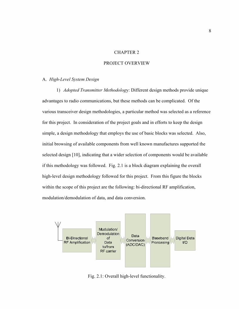
A. High-Level System Design 1) Adopted Transmitter Methodology: Different design methods provide unique
advantages to radio communications, but these methods can be complicated. Of the
various transceiver design methodologies, a particular method was selected as a reference
for this project. In consideration of the project goals and in efforts to keep the design
simple, a design methodology that employs the use of basic blocks was selected. Also,
initial browsing of available components from well known manufactures supported the
selected design [10], indicating that a wider selection of components would be available
if this methodology was followed. Fig. 2.1 is a block diagram explaining the overall
high-level design methodology followed for this project. From this figure the blocks
within the scope of this project are the following: bi-directional RF amplification,
modulation/demodulation of data, and data conversion.
Fig. 2.1: Overall high-level functionality.

9
The bi-directional RF amplification block amplifies RF signals passed to it from
the modulation/demodulation block and switch it onto the transmitting antenna. Also, it
will receive RF signals from the antenna and pass them over to the
modulation/demodulation block.
The modulation/demodulation block is in charge of taking the baseband analog
data from the data conversion block and modulating it up onto an RF carrier frequency.
It will then pass this modulated analog data to the bi-directional RF amplification block.
In turn, it will also take received RF signals from the bi-directional amplification block
and demodulate it back down to analog baseband to be passed to the data conversion
block.
The data conversion block will pass digital data between it and the baseband
processing block, and analog data between it and the modulation/demodulation block.
This block will receive digital data from the baseband processing block, convert it into
analog data, and send it off to the modulation/demodulation block. This block is bi-
directional, and hence it will also take analog data from the modulation/demodulation
block and convert it to digital data to be passed on to the baseband processing block.
From this transceiver methodology, the components that fall within the scope of
this project can be seen in greater detail in fig. 2.2. The design involves transmit and
receive paths. On the transmit path, In-phase and Quadrature sinusoidal signals (I&Q)
will be combined, modulated, and transmitted from the RFFE. On the receive path, RF
signals will be demodulated, separated into I&Q signals and passed to the baseband
processing block.

10
Fig. 2.2: RFFE block diagram (detailed).
2) Goals of Transmitter Design: With a design methodology selected, the options
available by actual components were optimized against the project goals. Again, the
primary goals of this project are to lower overall power consumption and physical size
while maximizing data rate. In order to lower overall power and physical size of the
system, as many blocks as possible need to be removed or combined onto a single
integrated circuit (IC). All the components in the design shown in fig. 2.2 are critical to
reliable operation of the transceiver, and hence cannot be removed. Therefore, the best
solution to minimize would be to take each of these blocks and place them into a single
Application-Specific Integrated Circuit (ASIC). Unfortunately, these types of ICs come
at an extreme cost, and hence are not an option for this project.
Initial manufacturer investigation indicated that there is a wide selection of
combination ICs that perform a group of the functions found in fig. 2.2. This solution
would take advantage of the power and size saving properties of ASICs while still
keeping project costs to a minimum. This route, of combining as many components onto

11 a single IC, was chosen in efforts to achieve the goals of this project. Minimizing the
number of ICs will lower the overall power consumption because the interfacing voltages
between ICs will be kept at a minimum. With fewer physical components, the overall
size of the RFFE will be reduced.
3) Board Layout: Additional design decisions were made in order to provide
easy isolation between this project and the rest of the radio system. This was achieved by
placing the RFFE and baseband processing systems on separate circuit card assemblies
(CCAs). Shown in fig. 2.3 is the physical separation of the RFFE and baseband
processing systems, referred to as the RF CCA and Digital CCA. All of the blocks that
fall within the scope of this project will be placed on the RF CCA and will interface to
the Digital CCA by a header connecting the two boards together.
This not only provides complete control over the assigned scope, but it also
provides good signal isolation between RF and digital signals. Different printed circuit
board (PCB) considerations must be taken into account when doing an analog circuit
design or a digital circuit design.
B. Project Timeline
1) Proof of Concept: The underlying uncertainties of this project coming from a
lack of experience and the uniqueness of the project goals, calls for a quick method to
Fig. 2.3: Circuit card layout.

12 prove the overall concept is possible. The proof of concept was done with the use of
evaluation boards of the selected components. These evaluation boards are provided
from the manufacture in order to quickly see test results of the component in the design.
A device can indicate on a data sheet its overall power consumption and other operating
characteristics, but physical testing of the device provides a clearer understanding of how
the device will behave, as well as assist in any design adjustments.
These evaluation boards can also be connected together to form a pseudo
prototype of the final design. In this manner, higher-level functionality can be evaluated.
Things such as overall power consumption and achievable data rate can be tested before
the efforts of a custom board design are expended.
2) Flow of Project: In order to efficiently use the time available, as well as insure
work is not done in vain, the flow of the project was established. Prior to a system design
involving a schematic and PCB layout, initial validation is performed with the evaluation
boards. Once these evaluation boards are working as desired, work on a custom board
design will proceed. This flow allows for the opportunity to redesign certain components
if the results obtained from the evaluation boards do not yield the anticipated information.
3) Gantt Chart: The bulk of this project is planned to occur during the 2009 year.
Shown in fig. 2.4 is the Gantt chart with the key milestones of the project as well as the
desired completion dates.

13
Table 2.1: PROJECT GANTT CHART

14
CHAPTER 3
RESEARCH AND INITIAL EFFORTS
A. Component Selection 1) Objectives and Design Requirements: In order to properly select components
that will aid in achieving the project goals, power, and size requirements of the RFFE
were quantified.
First, the power levels available to a payload on a CubeSat are typically on the
order of a few watts. The power generated by the solar panels on the CubeSat will
produce around 10 to 40 watts, depending on the solar panel design. With all the various
systems on the satellite, only a fraction of this overall power is available to the
transmitting radio. From this information, and additional guidance from personnel at the
Space Dynamics Laboratory (SDL), the overall consumed power by the RFFE is targeted
to 5 watts.
Second, the physical size of the radio needs to fit within the CubeSat standard.
However, the first revision of the RFFE will not be flown on an actual CubeSat. The
RFFE PCB size for this project will be minimized as much as possible and will serve as a
design guide for subsequent revisions. The volume of a typical CubeSat can be as small
as 10 centimeters cubed. The available payload area will allow for a transmitter PCB of
about 8 centimeters square. Quantitatively, the physical dimensions of the RFFE must be
less than 8 centimeters squared.
An additional concern in designing this CubeSat data link is the environmental

15 conditions of space flight. Without the protection of the atmosphere, CubeSats are
susceptible to high-energy subatomic particles and electromagnetic radiation. These
events can cause malfunctions in electronic circuitry. A common measure to prevent
such malfunctions is radiation hardening (RadHard). Some manufacturers of ICs provide
RadHard versions of their products. These ICs are equivalent in functionality to their
commercial grade counterparts, but the physical packaging and design method provides
greater resistance to such radiation upsets.
Building a transmitter that is RadHard qualified would be ideal, but there are a
number of factors that limit this as an option. Typical costs of RadHard components are
orders of magnitude more than their commercial equivalents. Also, manufacturers only
offer the RadHard option on a small subset of their components. The RadHard
equivalents require more power to operate, which conflicts with one of the project goals.
An additional discouragement to choosing RadHard components is that several CubeSat
missions have flown successfully with just commercial grade components [11].
2) Available Components: From initial investigation into different IC
manufacturers, two key companies appear to offer components that would satisfy the
established design constraints. These companies are Maxim Integrated Circuits and
Analog Devices Incorporated. Both these companies have a large library of RF devices
as well as proven solutions to RF transceiver problems. From these manufacturers,
components were compared and selected to design the most ideal configuration.
a) Maxim Integrated Circuits: Maxim Integrated Circuits (Maxim) have
eight different ICs that will satisfy the established design constraints. These eight ICs

16 belong to three different component families: Radio Frequency Integrated Circuit (RFIC)
transceivers, RFIC transmitters/receivers, and Analog Front Ends (AFE).
The first family of Maxim components is RFIC transceivers. These RFIC
transceivers have the ability to transmit and receive baseband I&Q data and modulate or
demodulate it to, or from, a carrier frequency. They provide several functions on a single
IC which satisfies the low power and physical size design constraints. They also have
sufficient bandwidth, up to 40MHz, to provide a high data rate connection. Conversely,
these ICs are frequency limited to the Industrial, Scientific, and Medical (ISM) bands at
2.4 and 5GHz. The part numbers for these ICs are: MAX2828, MAX2830, MAX2831,
and MAX2837 [12-15]. However, from this family of parts, the MAX2837 is not limited
to just an ISM band. Its operating frequency range is from 2.3-2.7GHz.
The second family of Maxim components consists of RFIC transmitters/receivers.
The transmitters will accept analog baseband I&Q data and modulate it up to a carrier
frequency. The receivers will take the modulated data and demodulate it back down to
I&Q analog baseband data. These ICs are all low power and highly integrated parts.
Yet, in order to have a complete system, two of these parts are required. The operating
frequency range of these parts does not include an ISM band. The part numbers for these
ICs are: MAX2112, MAX2120, and MAX2150 [16-18].
The last family of Maxim components investigated consists of a single AFE
device. This device has the ability to take analog I&Q data and convert it into digital
data. At the same time, it has the ability to take digital I&Q data and produce analog
data. This IC provides several functions on a single IC which satisfies the low power and

17 physical size design constraints. It also has sufficient bandwidth, up to 22MHz, to
provide a high data rate connection. The part number for this IC is: MAX19713 [19].
b) Analog Devices Incorporated: Analog Devices Incorporated (AD) has
nine different ICs that will satisfy the established design constraints. These nine ICs
belong to three different component families: RFIC transmitters, RFIC receivers, and
RFIC/AFE combinations.
The first family of AD components consists of RFIC transmitters. These RFICs
take baseband analog I&Q data and modulate them up to a carrier frequency. They have
a wide carrier frequency range from 0.4 to 2.7GHz. They also have sufficient bandwidth,
up to 160MHz, to provide a high data rate connection. The part numbers for these ICs
are: AD8346, AD8349, AD5372, and AD5375 [20-23].
The second family of AD components consists of RFIC receivers. These RFICs
take modulated data and demodulate it down to I&Q analog baseband data. They have a
wide carrier frequency range from .7 to 2.7GHz. They also have sufficient bandwidth, up
to 300MHz, to provide a high data rate connection. The part numbers for these ICs are:
AD5380 and AD5382 [24-25].
The third family of AD components consists of RFIC/AFE combinations. These
devices are transmit only and take baseband digital I&Q data and modulate them up to an
intermediate frequency (IF). They are highly integrated components that perform the
digital to analog conversion and the RF modulation of the data. They have sufficient
bandwidth, up to 400MHz, to provide a high data rate connection. The part numbers for
these ICs are: AD9856, AD9857, and AD9957 [26-28].

18 3) Decision Matrix on Component Selection: The abilities of each device were
placed within a spreadsheet (see Table 3.1). This spreadsheet compiles similar
characteristics of each device. With this spreadsheet, proper scores for a decision matrix
were produced.
From the information in Table 3.1, a decision matrix was formed. The
components are separated into two different categories. These categories are: RFIC and
AFE. Each component was scored on their corresponding features (see Table 3.2). For
the RFIC, the MAX2837 or MAX2150 will satisfy the design constraints the best.
However, the MAX2150 is a transmit-only device whereas the MAX2837 is a
transceiver. Therefore, the MAX2837 was selected as the RFIC device for this project.
For the AFE, the MAX19713 was clearly the best choice for this project.
Given the results of the decision matrixes, the best components for this project are
the MAX2837 for the RFIC and the MAX19713 for the AFE. With these two
components, full transceiver capabilities are possible. These two components combine
into two ICs all functionality of the components investigated. With only two ICs
performing the bulk of the analog processing, the overall power consumption will be low.
Additionally, the physical size of the project will consist primarily of just these two
components.
4) Additional Components Required: Some key functions of the RFFE are not
combined onto a single IC. These functions are as follows: Power Amplifier (PA), Power
Amplifier Driver (PAD), RF switch, and Band Pass Filter (BPF). Maxim and AD also
provide several options for these devices. The differences for these parts, between

19
Ta
ble
3.1:
KEY
CO
MPO
NEN
T C
HA
RT

20
Ta
ble
3.2:
DEC
ISIO
N M
ATR
IX

21 manufacturers, are minor enough that detailed comparisons were not performed.
Furthermore, each component selected has power regulation requirements. Because of
these requirements, a power regulation system must be designed. Following is a brief
discussion on each of these additional components and systems.
The PA selected is a Maxim MAX2247. This PA provides a maximum output
power of 900mW. The link budget for this project indicated the need for an RF
transmission power of 500mW. To account for potential loss in the transmission path,
the selection of a larger PA was debated. Yet, the PAs investigated appeared to operate
more efficiently when running near saturation. In efforts to keep overall power
consumption to a minimum, running the PA at its max efficiency is most important. This
device also comes in a small Ball Grid Array (BGA) package [29].
The PAD and RF switch were selected from a recommendation by an L-3
Communications Systems constituent [30]. The PAD selected is a Hittite HMC474SC70.
This PAD will amplify the transmit RF signal in preparation for the PA block. Its
frequency range is from direct current (DC) to 6GHz and it provides a gain of 13dB to
the input signal. Power consumption of this device is around 80mW and comes in a
SC70 package [31]. The RF switch is a Hittite HMC546LP2. This RF switch will
provide the switching between transmit and receive modes. This device comes in a 2x2
DFN package [32].
There was difficulty in selecting a BPF for this project. The filter manufactures
investigated provide a small set of standardized filters. Most filters, however, are custom
designs. The filtering range of interest for this project is 2.3-2.7GHz. This proved to be

22 an abnormally wide band for a filter. A custom filter design was requested, but the
resulting cost lead to selecting a standard filter. This BPF will pass frequencies from 2.2-
2.5GHz. Moreover, the narrower bandwidth filters were provided at no charge. The
filter selected is a FMD2530EGA donated by Microwave Vector [33].
The power regulation system is designed to provide required voltage levels to
each component on the RFFE. This regulation system will allow for a single input power
level to be provided to the board. A switching buck regulator was selected to provide
initial input voltage swing containment. Additional voltage regulators were selected for
each component. The switching regulator (SR) selected is a Linear Technologies
LTM4602HV. This switching buck regulator will take input voltages from 5 to 28 volts
and produce a 3.3 Volt output with up to 6 amps of current draw. The voltage regulators
for each device will be supplied from the 3.3 volt output of the SR. Eight different
voltage regulators will supply the various components of the RFFE. The combination of
the voltage regulators and switching buck regulator will provide needed power
conditioning for each component of the RFFE.
5) Carrier Frequency Selection: A high-level investigation into frequencies used
for CubeSat communication was performed prior to beginning the component selection
process. Four different frequency bands had been used for CubeSat communication, in
the past. Table 3.3 lists these frequency bands and their prescribed use by the Federal
Communications Commission (FCC). In light of the RFIC selected, the available carrier
frequencies for this project will be limited to 2.3-2.7GHz. This range of frequencies is
commonly referred to as S band. This band brings some valuable advantages for the

23 prototyping process. Within this range is an ISM band, as well as two satellite
communication bands. When testing the radio on the ground, the ISM band can be used
to avoid violating any FCC licensing regulations. When the radio is deployed, one of the
satellite bands can be used [34]. Unfortunately, the ISM band is highly occupied. This
will introduce legal challenges when applying for a portion of this band. Fortunately,
because of that same popularity, highly integrated components are available. Going to
another frequency band would increase overall size and power consumption of the
transmitter.
Table 3.3: CARRIER FREQUENCY INFORMATION
Band Frequency!Range Bandwidth FCC!defined!use FCC!Extended!Rules!IndexVHF!
(2!meter) 137"138MHz! 1MHz Satellite!Comms.(2!meter) 144"146MHz 2MHz Amature!Satellite!Comms.(2!meter) 146"148MHz 2MHz Amature!Radio(2!meter) 148"150.05MHz 2.05MHz Satellite!Comms. 5.218,!5.219,!G30
UHF(70!centimeter) 399.9"400.05MHz .15MHz Satellite!Comms. 5.26(70!centimeter) 400.15"403MHz 2.85MHz Satellite!Comms. 5.264,!US384,!US345,!US384(70!centimeter) 406"406.1MHz .1MHz Satellite!Comms. 5.266,!5.267(70!centimeter) 410"420MHz 10MHz Satellite!Comms. 5.268,!G5(70!centimeter) 460"470MHz 10MHz Weather!Satellites 5.287,!5.288,!5.289,!US201,!US209,!US216(33!centimeter) 902"928MHz 26MHz ISM!and!Amature 5.150,!US218,!US267,!US275
L"Band:(23!centimeter) 1.24"1.3GHz 60MHz Amature 5.332,!5.335,!5.282(21!centimeter) 1.39"1.392GHz 2MHz Fixed!Satellite 5.339,!US311,!US342,!US351,!US398(20!centimeter) 1.525"1.559GHz 34MHz Satellite!Comms. 5.341,!5.351,!5.356(20!centimeter) 1.559"1.6265GHz 67.5MHz GPS!Satellites …(20!centimeter) 1626.5"1660 33.5MHz Satellite!Comms. 5.341,!5.351,!5.375,!US342(17!centimeter) 1.675"1.71GHz 35MHz Weather!Satellites 5.289,!5.341,!US211
S"Band2"2.02GHz 20MHz Satellite!Comms. NG156
2.025"2.11GHz 85MHz Satellite!Comms. 5.391,!5.392,!US90,!US222,!US346,!US347,!US3932.18"2.3GHz 120MHz Satellite!Comms. NG168,!5.392,!US303
2.305"2.310GHz 5MHz Amature!Radio US3382.32"2.36GHz 40MHz Satellite!Comms. 5.396,!US3272.39"2.45GHz 60MHz Amature!Radio US276,!5.150,!5.2822.4"2.5GHz 100MHz ISM 5.150,!5.282,!US41,!5.402,!NG147,!US391
2.4835"2.5GHz 16.5MHz Satellite!Comms. 5.150,!5.402,!US41,!NG147,!US3913.3"3.5GHz 200MHz Amature!Radio 5.282,!US3423.6"4.2GHz 600MHz Satellite!Comms. US245,!US348,!US349,!NG180

24 B. Evaluation Kits Evaluation kits for each component were purchased to aid in the proof of concept.
Kits for the RFIC, AFE, PA, PAD, and SR were obtained. These evaluation boards can
be tested individually as well as together to see how each system will interact. Test
results of the evaluation boards can be found in Chapter 5.
C. Test Equipment and Software Packages 1) Lab Equipment: Along with the testing of the evaluation kits, specific test
equipment is needed in order to verify proper operation. Some of the evaluation kit data
sheets recommend certain test equipment [35-38]. This equipment consists of the
following devices: Spectrum Analyzer, Signal Generator, Oscilloscope, power supplies,
multi-meters, Logic Analyzer, Digital Pattern Generator, RF Power Meter, and a Data
Link Analyzer. A Logic Analyzer and a Digital Pattern Generator were not obtained for
this project. Each device and its use for this project are explained in the following
paragraphs.
The Spectrum Analyzer assists in displaying the RF spectrum of the various
analog signals. These signals consist of the actual RF transmissions as well as the
baseband I&Q values.
The Signal Generator will aid in simulating necessary signals to test the various
functions of each device. Various tones and even complex waveforms can be generated
and fed into the device of interest at precise power levels.
The Oscilloscope obtained for this project is a Digital Phosphorus Oscilloscope
that takes data samples at 20Gs/s. This device will provide the ability to look at the shape

25 of the analog signals. The sampling rate is high enough that analog signals of interest,
even at RF carrier levels, can be viewed and measured. It also has an embedded
computer to allow quick interfacing to programs such as MATLAB.
Several power supplies were needed for this project. Each evaluation board
requires about three power connections, each of which can vary in voltage level
depending upon the application. In conjunction with the power supplies, metering of the
voltage and current levels can be done with multi-meters.
The RF Power Meter will aid in measuring the overall RF power being emitted
from the transmitter system, as well as equipment calibration.
The data link analyzer will provide a bit error test. This device will send out a
known bit stream into the radio link and receive the same bit stream at the other end.
With this information, bit error rate measurements can be taken.
Shown in fig 3.1 is the lab bench setup for this project.
2) AFE Viewer Design: In order to simulate the digital interface without a Digital
Pattern Generator or Logic Analyzer, a digital interface was developed. This interface is
critical in testing the AFE evaluation board. Because of the uncertainties that would be
left unknown if the AFE went untested, it was decided to quickly design and implement a
substitute system called an AFE Viewer. By the use of a simple microcontroller, the
digital interface to the AFE can be tested. Shown in fig. 3.2 is the AFE Viewer system.
The key goal of this sub design is to quickly provide a digital AFE interface.
The AFE Viewer provides 10-bit transmit and receive interfaces to the AFE.
Additionally, 10 LEDs for the transmit and receive interfaces are provided to visually see

26
Fig. 3.1: Lab bench setup.
Fig. 3.2: AFE viewer system.
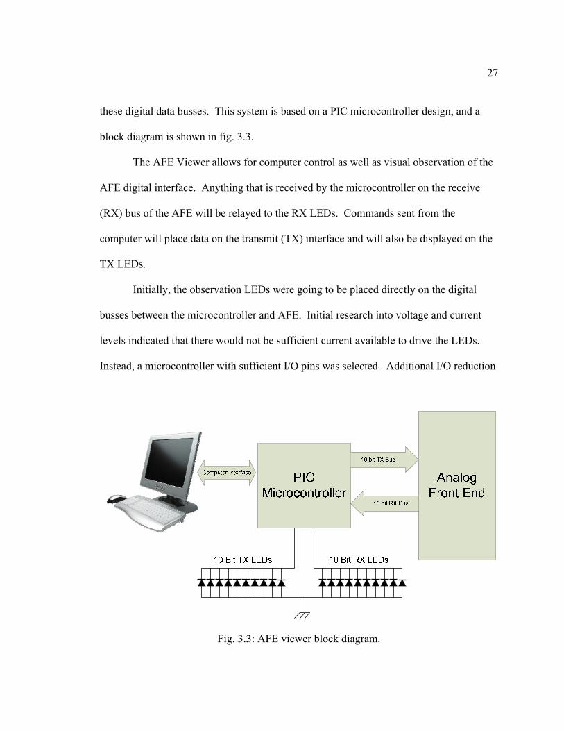
27
these digital data busses. This system is based on a PIC microcontroller design, and a
block diagram is shown in fig. 3.3.
The AFE Viewer allows for computer control as well as visual observation of the
AFE digital interface. Anything that is received by the microcontroller on the receive
(RX) bus of the AFE will be relayed to the RX LEDs. Commands sent from the
computer will place data on the transmit (TX) interface and will also be displayed on the
TX LEDs.
Initially, the observation LEDs were going to be placed directly on the digital
busses between the microcontroller and AFE. Initial research into voltage and current
levels indicated that there would not be sufficient current available to drive the LEDs.
Instead, a microcontroller with sufficient I/O pins was selected. Additional I/O reduction
Fig. 3.3: AFE viewer block diagram.

28 methods could have been employed, but the main goal of this design was to quickly
produce a working interface to the AFE. Shown in fig. 3.4 is the electrical schematic
developed for the AFE Viewer.
A short software program was developed to display the RX data bus as well as
control the TX bus. Shown in fig. 3.5 is a flow diagram of the software. The C code
used for this device can be found in Appendix A.
The microcontroller performs this cycle at about one kilohertz. This cycle is not
fast enough for final product equipment, but during initial testing of the AFE, the
performance speed was sufficient. Results obtained by the AFE Viewer system are
Fig. 3.4: AFE viewer schematic.

29
Fig. 3.5: AFE viewer software flow.
discussed in Chapter 5.
3) Software: Beyond the hardware selected, some software packages are needed.
These packages will allow for analysis of data collected from test equipment and aid in
schematic and PCB layout development. These software packages are MATLAB and
Eagle.
The MATLAB software used resides on the Oscilloscope. A unique interface
between the oscilloscope hardware and its embedded computer allows MATLAB to
capture data from the oscilloscope probes. With this ability, mathematical operations can
be performed on raw data. However, this functionality was not working properly at the

30 beginning of the project. Software modifications were needed in order to get this
interface working. By using .m file MATLAB scripts, a user interface was developed.
This interface provides the user with standard oscilloscope functions and brings the
selected data into the MATLAB environment.
Eagle, from CadSoft, is a schematic capture and PCB layout program. This
software package links schematic drawings to a PCB layout editor, to allow accurate
development of PCBs. This software also allows for the design of multi layer PCBs—a
necessity in miniaturizing physical size of the RFFE.

31
CHAPTER 4
DESIGN
A. RFIC Subsystem Design
As indicated in Chapter 3, the bulk of the analog processing occurs on a single IC,
referred to as the RFIC. This RFIC is the MAX2837 broadband transceiver. Within this
package, analog processing for both transmit and receive paths occurs. See fig. 4.1 for a
block diagram of the various function that occur within this IC [15].
Fig. 4.1: MAX2837 block diagram.

32
This RFIC has two analog paths. On the transmit path, differential I&Q data are
inputted into the IC. From there, these signals are filtered, modulated, mixed, and
amplified, prior to being outputted for final external processing. On the receive path, a
differential RF signal is received, amplified, demodulated, filtered, and then amplified
again, prior to being outputted for further baseband processing.
This RFIC comes in a 48 pin Thin Quad Flat No leads (TQFN) package. This
package provides a substantial amount of the required analog processing on a single IC.
The advantages of this IC are its small physical size and low-power consumption.
However, in order to obtain proper operation of this RFIC, power requirements, RF
considerations, and additional circuitry, were taken into account.
1) Power: This RFIC requires 11 different power supply connections for proper
operation. These supplies each provide power to different processing blocks within the
IC. Due to the sensitive nature of analog processing, a single supply into the IC is not
supported. Each processing block needs capacitive isolation between the others in order
to maintain satisfactory noise figures throughout the device. The separate voltage
supplies are as follows: RX Low Noise Amplifier (LNA), Internal Oscillator, Phase
Lock Loop (PLL), External Reference Clock, TX Power Amplifier Driver (TXPAD), TX
Mixer (TXMX), RX Mixer (RXMX), RX Baseband I Amplifier (RXBB1), RX Baseband
Q Amplifier (RXBB2), Phase Lock Loop Charge Pump, and Digital Circuitry.
According to the data sheet for this device, the overall current consumption should not
exceed 170mA [15]. This indicates, that in full operation, the device should consume
around 500mW, about 10% of the RFFE’s power budget.

33 Even though each of the 11 supply lines have been brought out separately from
the IC, with some external capacitance in place, a number of these lines can be fed from
the same voltage regulator. By doing this, the eleven supply lines can be fed from only
three voltage regulators. These regulators will be discussed further in section G of this
chapter.
2) RF Considerations: Certain requirements exist in regards to the analog
interfaces on the device. Differential analog connections are required on the I&Q
interfaces. These interfaces come at an advantage for moving analog signals across a
PCB layout. The RX and TX ports of the RFIC are differential as well. Prior to
connecting this interface to the external amplification systems, RF switch, and antenna,
the differential signals need to be converted into single ended signals. This conversion is
done by the use of high frequency transformers known as Baluns. The Phase Lock Loop
(PLL) circuit is placed as close as possible to the actual IC to minimize trace impedance
incurred by the characteristics of the PCB. Each of the differential analog interfaces
require 100 Ohm impedance connections. These connection requirements are satisfied
with proper PCB trace design and subsequent subsystem interface matching.
3) Additional Circuits Required for Operation: Beyond the analog considerations
taken into account, some additional systems, external to the IC, are required for proper
operation. The RFIC requires a 40MHz reference oscillator for precise timing of critical
systems. A number of methods could have been employed in order to produce this
reference. The method chosen is a Temperature Compensated Oscillator (TCXO). These
oscillators are tuned with high precision, and do not require additional subsystems for

34 proper operation.
Additional passive circuit networks are included on the RX and TX lines, as well
as the I&Q interfaces. These circuit networks allow for additional filtering and
debugging, once the PCB board has been produced. The need for these networks on the
final revision is unclear. Still, these networks are minimal in size and do not require any
external power compensation.
B. AFE Subsystem Design
In addition to the RFIC, a large portion of the remaining processing will take
place on the Analog Front End (AFE). The AFE selected is the MAX19317. Within this
package, signal conversion from analog-to-digital, and from digital-to-analog will occur.
See fig. 4.2 for a block diagram of this IC [19].
This AFE has two data paths. On the transmit path, 10-bit digital I&Q data is
brought into the device at double data rate. Then, with timing adjustments, it is converted
to differential analog I&Q signals. From there, the signals are outputted from the device.
On the receive path, differential I&Q signals are converted to 10-bit digital signals. They
are then multiplexed onto the digital receive bus at double data rate.
This device also provides three additional digital-to-analog converters and two
additional analog-to-digital converters. One of these additional analog-to-digital
interfaces is used for the Received Signal Strength Indicator (RSSI) that comes of the
RIFC. The main RX and TX paths, as well as the additional data converters are all
controlled by an SPI interface to the IC.
This AFE comes in a 56-pin TQFN package. This package performs the required

35 analog-and-digital data conversions on a single IC. The advantages of this IC are its
small physical size and low-power consumption. However, in order to obtain proper
operation of this AFE, power requirements, RF and digital considerations, and additional
circuitry were taken into account.
1) Power: The AFE requires two different voltage regulators, one for the analog
processing and the other for the digital processing. The analog processing portion
requires 3.3 volts for proper operation. The digital supply can vary in order to properly
interface to the digital processing system. For this project the AFE will be directly
Fig. 4.2: MAX19713 block diagram.

36 interfaced with an FPGA that runs its digital I/O pins at 2.5 volts. Hence, the digital
interface voltage for the AFE will be 2.5 volts. According to the data sheet for this
device the overall current consumption should not exceeded 37mA [19]. This indicates
that in full operation the device should consume around 122mW, about 2% of the RFFE’s
power budget. The voltage regulators for this device will be discussed further in section
G of this chapter.
2) RF Considerations: The analog I&Q interfaces on the AFE can operate from a
common mode voltage of zero with +- 400mV variance. These analog interfaces also
need to be matched to 100 ohms. Similar to those requirements found on the RFIC. The
additional analog inputs have similar common mode voltage and peak to peak voltage
requirements.
3) Digital Considerations: The digital interface of the AFE has a maximum
transition time of 90MHz. The AFE is capable of receiving a 45MHz clock frequency
while the I&Q data are brought in at double data rate. The In-Phase sample is brought
into the AFE on the rising edge of the clock and the Quadrature sample is brought in on
the falling edge. The digital interface requires an additional circuit to assist in the proper
handling of digital signals.
4) Additional Circuits Required for Operation: To aid in settling the high-
frequency digital transients, series resistors have been placed on all high-frequency
digital lines. These resistors have been placed in recommendation by the evaluation kit
to assist in proper digital data sampling. The resistor values, along with the inductance in
the PCB traces will act as a low-pass filter and reduce the transient response of each

37 digital line.
Beside these transient dampening resistors, a reference voltage circuit network
has been implemented. This provides proper reference offset voltages to the incoming
I&Q signals. This circuitry will allow for various voltage offsets and biases to be
implemented, with proper selection of series and parallel resistor values.
C. PAD Subsystem Design
Once the TX signal is presented at the output of the RFIC, it must be amplified,
prior to being fed into the PA. This amplification is done with a PAD. With a design
requirement of 500mW total output power, a PA was selected which has the ability to
output the required amount of power. The gain of this PA is 24dB. The output power of
the RFIC is, at best, 0dBm. An additional gain of 3dB is required in order to obtain an
output of 27dBm or 500mW. However, the RFIC has the ability to attenuate the output
power down to -45dBm. In order to utilize the full range of the RFIC and PA, the gain of
the PAD was selected to be a constant 16dB. The part chosen is a Hittite HMC474SC70.
This will allow for a dynamic output power range from -29dBm to 40dBm. The PA is
not capable of this much output power, but this will allow for compensation due to PCB
losses and other insertion losses from the BPF and RF switch.
According to the data sheet for this device the overall current consumption should
not exceeded 35mA [31]. This indicates that in full operation the device should consume
around 115mW, about 2% of the RFFE’s power budget. This device only requires one
voltage regulator. In order to isolate between RF stages, a separate voltage regulator is
used to supply power to this component. Section G in this chapter discusses in more

38 detail the voltage regulator selected for the PAD.
D. PA Subsystem Design A PA has been integrated into the design in order to amplify the signal from the
RFIC to the design requirement of 500mW. The PA will take the output of the PAD,
mentioned in section C, and provide the last amplification prior to radiating off the
antenna. The PA selected can supply up to 500mW and has an integrated impedance
matching circuit. This circuit allows for ease of integration without risking the possibility
of damaging the PA from either transmitting with no antenna, or with a poorly matched
antenna. The device selected for the PA is the Maxim MAX2247. This PA offers
500mW total output power and includes a bias input output power regulation.
According to the data sheet for this device the overall current consumption should
not exceeded 350mA [29]. This indicates that in full operation the device should
consume around 1.155W, about 23% of the RFFE’s power budget. This device requires
a single voltage regulator. Section G in this chapter discusses in more detail the voltage
regulator selected for the PA.
E. RF Switch Subsystem Design Since this project contains both a transmitter and receiver, and to avoid the use of
two antennas, an RF switch was implemented to allow switching between RX and TX
modes. This device is not part of the final CubeSat transmitter, and hence an RF switch
that satisfied basic insertion loss levels was selected and implemented. The part chosen
is a Hittite HMC546LP2. This device acts as a double throw single pole (DTSP) switch.

39 This switching functionality will allow for the receive path to access the antenna, as well
as allow the transmit path the same antenna access at different time intervals. The control
of this device is done by a single digital voltage level input, which will be controlled by
the FPGA.
The data sheet does not call out overall current consumption of this device. The
cost of this evaluation board is beyond budget. The data sheet does provide a maximum
overall power dissipated rating [32]. This value is the amount of RF power that can be
sent across the TX path to the antenna. The voltage regulator for the RF switch was
selected to allow for full power dissipation. Section G in this chapter discusses in more
detail the voltage regulator selected for the RF switch.
F. Band Pass Filter Selection The last component prior to the antenna connection is a band pass filter. This is a
static passive device that provides general filtering of unwanted RF power outside the
band of interest. Most surface mount filters are custom made, and have very narrow
bandwidths, whereas the requirements of this radio are to operate over a much wider
band. A custom wideband filter could have been developed, but would have been much
more costly to produce. Because of the cost involved, a narrower band filter that already
existed was selected. This filter will pass frequencies from 2.2-2.5GHz. Slightly offset
from the 2.3-2.7GHz abilities of the RFIC. This component will provide sufficient
filtering for this revision of the board. This filter is a passive device, and requires no
additional voltage regulators or passive components for proper operation.

40 G. Power Subsystem Design The final subsystem for this design is the power regulation system. Each of the
components discussed in sections A through E of this chapter require some form of
power regulation. A switching buck regulator (SR) was also added in order to isolate the
supply power from the voltage regulators. This SR will supply 3.3 volts to each of the
voltage regulators. The part chosen is from Linear Technologies and is a LTM4602HV.
It will take an input voltage from 5 to 28 volts and can source up to 6 amps of current at
3.3 volts [39]. The switching buck regulator will not be needed on the following RFFE
revision, as exact voltages and current levels available on CubeSat systems will be further
explored.
1) Power Supply Requirements: The RFFE subsystems require, in total, eight
voltage regulators: three for the RFIC, two for the AFE, and three for the remaining
transmit RF amplification/switching devices. Each of these regulators are in accordance
with the current and voltage specifications found on the data sheets of the devices they
supply. In Table 4.1 the various power supply requirements of each device and the
selected components are displayed [40-44].
The RFIC requires three voltage regulators. Each of these regulators supplies
Table 4.1: VOLTAGE REGULATOR REQUIREMENTS

41 2.85 volts to the RFIC. Of these three, two regulators supply up to 120mA and the other
supplies up to 300mA. The first two are both Maxim part number MAX8510EXK29.
One of these MAX8510EXK29 will be used to power the Reference Oscillator, PLL,
Charge Pump, and Transmit Oscillator subsystems. The other MAX8510EXK29 will be
used to power the VCO subsystem. The final regulator is a MAX8887EZK29 and it will
be used to power the LNA, TXPAD, TXMX, RXBB1, RXBB2, and RXMX subsystems.
These three regulators were selected from the MAX2837 evaluation kit data sheet.
The AFE requires two voltage regulators. These voltage regulators vary in
voltage, but not in current. They both will supply 150mA to the AFE, though one will
supply 3.3 volts while the other will supply 2.5 volts. The 3.3 volt regulator will power
the core of the AFE. The 2.5 volt regulator will power the digital interface. These two
regulators were selected from Maxim’s library of regulators.
The PAD, PA, and RF switch each have their own voltage regulators, each
supplying 3.3 volts to their prospective counterparts. The PAD’s voltage regulator
supplies 150mA. The PA and RF Switch’s voltage regulators supply 500mA. As with
the AFE regulators, these regulators were also chosen form Maxim’s library of
regulators. Shown in fig. 4.3 is a complete block diagram of the voltage regulation
subsystem.
Each of these voltage regulators requires input power of at least 3.3 volts.
Because the regulated voltages are also 3.3 volts or 2.85 volts, the operating efficiency of
the voltage regulators will remain high. The regulators will only loose efficiency when
smoothing out AC upsets on the supply lines.

42
Fig. 4.3: Voltage regulation block diagram.
2) Initial EMI Considerations: An important part to electronic system design is
electromagnetic interference (EMI). Electronic devices must be able to withstand
specified amounts of EMI as well as restrict their own production of EMI. EMI can
propagate throughout a system by electrical traces or by RF radiation. In order to
dampen EMI on the RFFE, basic filtering on each stage of voltage regulation and analog
processing has been implemented. No specific EMI avoidance measures have been
designed into this project.
H. Full RFFE System Design 1) Overall Design: With the design of each subsystem completed, the overall
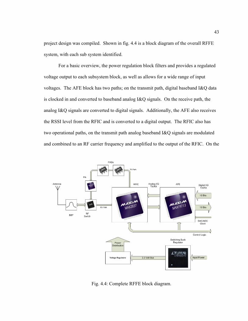
43 project design was compiled. Shown in fig. 4.4 is a block diagram of the overall RFFE
system, with each sub system identified.
For a basic overview, the power regulation block filters and provides a regulated
voltage output to each subsystem block, as well as allows for a wide range of input
voltages. The AFE block has two paths; on the transmit path, digital baseband I&Q data
is clocked in and converted to baseband analog I&Q signals. On the receive path, the
analog I&Q signals are converted to digital signals. Additionally, the AFE also receives
the RSSI level from the RFIC and is converted to a digital output. The RFIC also has
two operational paths, on the transmit path analog baseband I&Q signals are modulated
and combined to an RF carrier frequency and amplified to the output of the RFIC. On the
Fig. 4.4: Complete RFFE block diagram.

44 receive path, the received signal is amplified and demodulated into analog baseband I&Q
differential signals. The PAD takes the transmit output of the RFIC and amplifies it in
preparation for the PA stage. In the PA stage, final amplification of the RF signal is
preformed. Overall amplification can be adjusted with a bias input to the PA or by an
attenuation control on the RFIC. The RF switch provides the switching means to allow
the transmit and receive paths to share the same antenna at different times. And finally, a
band pass filter is on the front end of the radio to allow signals of interest to pass through,
while blocking any adjacent bands.
2) Schematic: The schematic for this project was developed by altering the
evaluation kit schematics as well as integrating the required components not evaluated.
See Appendix B for the RFFE schematic drawings. Page one of the schematic is the
RFIC subsystem. Here the RFIC, reference oscillator, and phase lock loop circuit are
shown. As per recommendation by the data sheet and evaluation kit, decoupling and
filtering capacitors were placed in various locations such as supply pins and other
frequency sensitive areas of the device [36].
Page two of the schematic is the AFE subsystem. This schematic displays the
decupling capacitors placed on the various supply lines as well as the regulator voltage
circuitry and dampening resistor networks for the digital interface.
Page three of the schematic is the passive filter networks. Both the transmit and
receive I&Q baseband legs and the RF carrier TX and RX legs are drawn here. Each of
these networks allows for passive filtering to be implemented if needed, depending upon
the behavior of each leg on the actual PCB traces.
45 Page four of the schematic is the amplification and switching stages of the radio.
This schematic displays the decupling capacitors placed on the various supply lines as
well as the transmission line conditioning.
Page five of the schematic is the voltage regulation subsystem. The large IC is
the switching buck regulator and the subsequent smaller blocks represent each individual
voltage regulator. Each regulated line is then branched to individual supply pins. The
zero ohm resistors on each of these paths provide a way to disable portions of the radio if
needed.
Page six of the schematic is the header interface for the radio board. This header
will provide access to the control lines as well as the digital bus interface. It also has pins
allocated for supplying power to the board. With the RFFE power supplied through this
header, a mother board can have complete control of the RFFE.
3) PCB Layout: In efforts to keep the physical size to a minimum, a 4-layer PCB
board is needed. Each layer was broken into sections to assist in isolating between
different types of signals. Proper micro strip traces for the RF portions of the RFFE
yielded to be the most difficult portion of the PCB layout. Picket fence ground isolation
between RF signals and any other signal levels were implemented to further isolate the
RF from the rest of the board design. Once the RFFE layout was established, the finish
size of the PCB was increased to fit the PIC-104 standard [45]. This standard is used at
SDL for CubeSat electronics.
Appendix C is the RFFE PCB layout. Page one is the top layer. This layer
contains the majority of the RFFE devices, as well as the RF traces and digital AFE

46 traces. Page two is the first inner layer. This layer is used for horizontal and lower PCB
trace runs. Page three is the second inner layer. This layer is used for vertical and upper
PCB trace runs. Page four is the bottom layer. This layer holds the RFFE header
interface and additional devices. Page five is the complete PCB layout.
I. Antenna Selection Initial design efforts were going to include the design of a custom antenna for the
project. However, priority of other components of the project overtook the antenna
design effort. A wide selection of antennas exists that have been designed for small
applications such as CubeSats, and hence a custom design risks repeating work that has
already been done. Initial antenna research indicates that most CubeSat systems use
dipole or patch antennas for communications [12]. For testing, monopole antennas are
used. These were readily available and have proper RF matching at the ISM frequency
band. See the future work section in Chapter 6 for more information on antenna efforts.
J. Adapter Board Design With the compact physical size of the RFFE, an adapter board to interface other
digital equipment was designed. This adapter board provides a method for digital devices
to connect to the RFFE. The adapter board was specifically designed for the Vertex 5
FPGA evaluation board, but can be adapted to any digital device. This board has also
been designed to allow full mounting of the RFFE. The schematic is found in Appendix
D.
Appendix E is the adapter board layout. This board has four layers, like the

47 RFFE. Page one is the top layer. This layer contains the header for connection to the
RFFE and a separate header to provide access to each RFFE control signal. Page two is
the first inner layer. This layer is used to provide a path for the analog to digital bus.
Page three is the second inner layer. This layer is used to provide a path for the digital-
to-analog bus. Page four is the bottom layer. This layer provides a path for the digital
control signals, as well as holds the FPGA evaluation board headers. Page five is the
complete PCB layout.

48
CHAPTER 5
RESULTS
A. Evaluation Kit Results The evaluation kits provide a base understanding of how the radio will operate.
This knowledge aids in improving the RFFE design. The following sections present the
data obtained from tests performed on the evaluation kits. The kits were tested both
individually and together.
1) Individual: Each evaluation board comes with a data sheet which includes
instructions on how to operate the device. These instructions were followed for each
device. The measured results were compared with what the data sheet indicates the
results should be. Any discrepancies were investigated and corrected if needed.
a) RFIC: Shown in fig. 5.1 is the RFIC evaluation board. Two tests were
performed on this device, a transmit test and a receive test. Prior to running these tests,
the frequencies of the reference oscillator and output clock signals were measured. The
data sheet indicates that the reference oscillator should run at 40MHz, and the reference
clock should be 20MHz [36]. Figures 5.2 and 5.3 are the waveforms acquired by
MATLAB, via the oscilloscope interface. Both of these clock signals appear to be within
a few kilohertz of the specified frequency.
On the transmit test, two sinusoidal tones, 5MHz and 10MHz, were respectively
applied to the I&Q baseband inputs. According to the data sheet, the RFIC will combine
and mix these tones with a selected local oscillator (LO) [36]. The frequency selected for

49
Fig. 5.1: RFIC evaluation board.
Fig. 5.2: RFIC 20MHz reference clock.
-10 -8 -6 -4 -2 0 2 4 6 8
x 10-8
0
0.05
0.1
0.15
0.2
0.25
Am
plitu
de (V
)
Time (s)
20MHz Reference Clock

50
Fig. 5.3: RFIC 40MHz reference oscillator.
this test was 2.5GHz. This produces four sinusoidal tones near the LO frequency, one at
±10MHz, and the other at ±5MHz. Figure 5.4 is a spectral reading of the RF output. The
center frequency is 2.5GHz and the corresponding tones can been seen at ±5MHz and
±10MHz. The yellow or lower of the two traces indicate the gain of the RFIC under
normal conditions. The blue or upper trace is the output gain obtainable if the mixer gain
in increased. The output power could be increased by an additional 10dB, but the cost of
this increase would be more LO leakage. As shown in fig. 5.4, the LO leakage at this
gain is about 24dBm lower than the signals of interest.
While testing the transmitter, the overall current consumed by the device was
174mA at 3.3 volts. The data sheet indicates that the consumed current at 3.3 volts,
during transmit mode, is nominal around 145mA [36]. The measured current is higher
than the specified value. This can be attributed to computer interface circuits on the
-10 -8 -6 -4 -2 0 2 4 6 8
x 10-8
-0.08
-0.06
-0.04
-0.02
0
0.02
0.04
0.06
0.08A
mpl
itude
(V)
Time (s)
40MHz Reference Oscillator
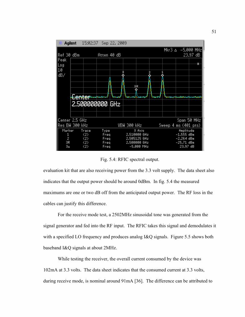
51
Fig. 5.4: RFIC spectral output. evaluation kit that are also receiving power from the 3.3 volt supply. The data sheet also
indicates that the output power should be around 0dBm. In fig. 5.4 the measured
maximums are one or two dB off from the anticipated output power. The RF loss in the
cables can justify this difference.
For the receive mode test, a 2502MHz sinusoidal tone was generated from the
signal generator and fed into the RF input. The RFIC takes this signal and demodulates it
with a specified LO frequency and produces analog I&Q signals. Figure 5.5 shows both
baseband I&Q signals at about 2MHz.
While testing the receiver, the overall current consumed by the device was
102mA at 3.3 volts. The data sheet indicates that the consumed current at 3.3 volts,
during receive mode, is nominal around 91mA [36]. The difference can be attributed to

52
Fig. 5.5: RFIC RX baseband tones.
the additional components on the evaluation kit used for interfacing to the computer.
A simultaneous transmit and receive test was performed to acquire the overall
current consumed during full duplex operation. The overall consumed current was
175mA at 3.3 volts. The data sheet does not clearly call out what this value should be.
The measured value was only a few milliamps above the transmit mode and because this
mode will never be used in the design, the measurement was rescored for documentation
purposes only.
b) AFE: Shown in fig. 5.6 is the AFE evaluation board. Two tests were
performed on this device, a transmit test and a receive test. Due to the lack of a Digital
Pattern Generator, the AFE was tested initially against the AFE Viewer and then against
the FPGA evaluation board. On the tests performed with the AFE Viewer, the clock
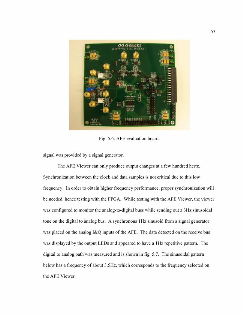
53
Fig. 5.6: AFE evaluation board. signal was provided by a signal generator.
The AFE Viewer can only produce output changes at a few hundred hertz.
Synchronization between the clock and data samples is not critical due to this low
frequency. In order to obtain higher frequency performance, proper synchronization will
be needed, hence testing with the FPGA. While testing with the AFE Viewer, the viewer
was configured to monitor the analog-to-digital buss while sending out a 3Hz sinusoidal
tone on the digital to analog bus. A synchronous 1Hz sinusoid from a signal generator
was placed on the analog I&Q inputs of the AFE. The data detected on the receive bus
was displayed by the output LEDs and appeared to have a 1Hz repetitive pattern. The
digital to analog path was measured and is shown in fig. 5.7. The sinusoidal pattern
below has a frequency of about 3.5Hz, which corresponds to the frequency selected on
the AFE Viewer.

54
Fig. 5.7: AFE output from AFE viewer.
The current consumed during this test with the AFE Viewer, was measured to be
47mA at 3.3 volts. The data sheet indicates that the current consumed in this operation
mode should be around 32mA [35]. This difference can be attributed to the additional
components on the evaluation kit used for interfacing to the computer.
The AFE was also tested with the FPGA evaluation board. Only the transmit
direction of the AFE was tested. In this configuration, the clock input to the AFE was
generated by the FPGA. Shown in fig. 5.8 is the clock signal generated. The frequency
of the clock signal measured is approximately 41MHz.
The FPGA was programmed to generate I&Q data samples at double the rate of
the clock frequency, as required in the AFE specification [35]. With user input on the
FPGA, selectable frequency tones were produced on the I&Q channels. Shown in figs.
5.9 and 5.10 are the I&Q analog outputs of the AFE when a 5MHz frequency selected.
-1 -0.8 -0.6 -0.4 -0.2 0 0.2 0.4 0.6 0.8
-5
-4
-3
-2
-1
0
1
2
3x 10⁻³
Am
plitu
de (V
)
Time (s)
AFE Output from AFE Viewer
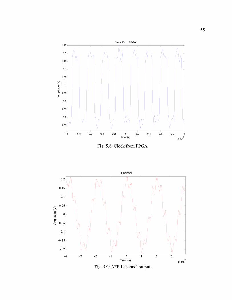
55
Fig. 5.8: Clock from FPGA.
Fig. 5.9: AFE I channel output.
-1 -0.8 -0.6 -0.4 -0.2 0 0.2 0.4 0.6 0.8 1
x 10-7
0.75
0.8
0.85
0.9
0.95
1
1.05
1.1
1.15
1.2
1.25
Am
plitu
de (V
)
Time (s)
Clock From FPGA
-4 -3 -2 -1 0 1 2 3
x 10-7
-0.2
-0.15
-0.1
-0.05
0
0.05
0.1
0.15
0.2
Am
plitu
de (V
)
Time (s)
I Channel

56
Fig. 5.10: AFE Q channel output.
The measured analog output signals are very close to the anticipated signals
produced by the FPGA. Initially, some synchronization issues existed, but these
pertained to the programming of the FPGA.
The current consumed during this tests was measured to be 51.5mA at 3.3 volts,
the data sheet indicates that the current consumed in this operation mode should be
around 32mA [35]. The difference can be explained by two items not mentioned in the
data sheet. First, a portion of the difference can be attributed to the additional
components on the evaluation kit, used for interfacing to the computer. The second
portion of the difference is because of the interface differences between the FPGA and
AFE Viewer. The FPGA has a 2.5 volt digital interface, and the AFE Viewer has a 3.3
volt interface. Hence, about the same amount of power is being supplied, just at a
different voltage and current level.
-4 -3 -2 -1 0 1 2 3
x 10-7
-0.2
-0.15
-0.1
-0.05
0
0.05
0.1
0.15
0.2
Am
plitu
de (V
)
Time (s)
Q Channel

57 c) PAD: Shown in fig. 5.11 is the PAD evaluation board. The PAD
provides a constant gain of the RF signal over the desired frequency range. This device
is tested by passing various carrier frequency tones within the range of 2.3-2.7GHz.
These tones are produced by a Signal Generator, and the gain difference is measured on a
Spectrum Analyzer. The input power and output power are measured. The difference
between these indicates the gain.
The input power is adjusted close to the point of saturation for the PAD, prior to
taking measurements. The input power is increased until a nonlinear gain is achieved.
At this point, the input power is lowered slightly to insure operation in the linear range of
the PAD. At this point, the maxim current and gain are obtained. The maximum input
power, without entering saturation, was found to be -5dBm
A frequency sweep across the band of interest is performed. Shown in fig. 5.12 is
Fig. 5.11: PAD evaluation board.

58 the gain difference between the input signal and the amplified output signal. The gain of
this device appeared to be a constant 12dB. The data sheet specifies a gain of 13dB for
this frequency range [31]. The slight difference can be attributed to cable loss.
Additional tests are performed to find the max output power. The max output power was
found to be 10dBm, with an input power of 7dBm. The current consumed by the PAD
was measured to be 25mA at 3.3 volts. The measured current is exactly that specified in
the data sheet [31].
d) PA: Shown in fig. 5.13 is the PA evaluation board. The PA provides
the final amplification of the RF signal prior to radiating on the antenna. This device is
tested by passing various carrier frequency tones within the range of 2.3-2.7GHz. These
tones are produced from a Signal Generator and the output is measured
Fig. 5.12: PAD gain.

59 on a Spectrum Analyzer. The input power and output power are measured. The
difference between these indicates the gain.
The input power is adjusted close to the point of saturation for the PA, prior to
taking measurements. The input power is increased until a nonlinear gain is achieved.
At this point, the input power is lowered slightly to insure operation in the linear range of
the PA. Here, the maxim current and gain are obtained. The maxim output power,
without entering saturation, was found to be 24dBm. A frequency sweep across the band
of interest is performed. Shown in fig. 5.14 is the gain difference between the input and
output signals. The gain across the frequencies of interests appears to be quite linear,
with an average gain of 24dB. The data sheet indicates the same gain across this
frequency range [37].
The current consumed by the PA was measured to be 330mA at 3.3 volts. The
Fig. 5.13: PA evaluation board.

60 data sheet specifies a power consumption of about 315mA [37]. The difference is due to
the fact that the input power was driven two high in order to overcome cable loss. This
drove the PA slightly into saturation.
e) RF Switch: The RF switch was not evaluated due to the high cost of
the evaluation kit. With the assumed simplicity of the device, and according to the data
sheet, operational details were assumed. Details such as insertion loss and overall current
consumption were taken directly from data sheet values. If needed, independent testing
of the RF switch can be performed on the RFFE.
2) Joint: With each component more fully understood by individual investigation
on their respective evaluation boards, the boards were connected together to evaluate
joint operation and interaction. Shown in fig. 5.15 is the simulation setup of the RFFE
Fig. 5.14: PA gain.

61
Fi
g. 5
:15:
Ful
l RFF
E w
ith e
valu
atio
n ki
ts.

62 design with evaluation kits.
Because interaction between the FPGA and AFE had already been explored, joint
testing was started from that point. From there, each additional system was added in
turn: the RFIC onto the AFE, then the PAD onto the RFIC, and finally the PA onto the
PAD. Each stage was added on when the previous stage was found to be operating
properly.
The overall system composed of all the evaluation boards connected together,
appears to be operating as anticipated. Baseband I&Q tones are generated from the
FPGA and sent through the RFFE. Shown in fig. 5.16 is the transmitter output of the
RFFE. This figure displays the I&Q tones modulated and amplified about the LO
frequency.
Fig. 5.16: Transmitter output from the RFFE evaluation kits.

63 An unanticipated issue arose during the joint testing of the RFFE evaluation
boards. While adjusting gain parameters on the RFIC, 40MHz harmonics of the signals
of interest were introduced. Shown in fig. 5.17 is the Spectrum Analyzer measurement of
the tone harmonics.
It was found that when maximizing the gain output of the RFIC these harmonics
are introduced. Subsequent gain stages amplify these harmonics out of the noise floor.
Lowering the power output of the RFIC minimizes these harmonics. However, it also
lessens the overall transmission power of the RFFE. In order to compensate for this loss
in transmission power and additional PAD was introduced into the RFFE.
In addition to the harmonics, the overall output power did not get above 24dBm.
Further investigation of the PA divulged that its maximum power output is only 24dBm.
Fig. 5.17 Unwanted 40MHz harmonics.

64 This was misunderstood when selecting this component. With this PA only 250mW of
output power can be obtained. A different PA will need to be selected for future
revisions of the RFFE.
During the joint testing of the RFFE evaluation kits, the overall current
consumption was monitored. The Switching Regulator’s evaluation kit was used to
supply power to each evaluation kit in the RFFE. The current was measured both on the
SR input and output. When maximum output power was obtained, the 3.3 volt SR output
was measured to be 384mA. The input to the SR at 5 volts was measured to be 279mA.
Hence, the overall power consumed by the RFFE should be less than 1.5 watts. With a
power budget of 5 watts, this provides ample room for a higher power PA. Without
enabling the PA, overall power consumption is under 1 watt.
B. RF Frontend CCA 1) Manufacturing: The manufacturing of the RFFE and Adapter Boards required
a significant effort in project management and coordination between different
manufacturing companies. After working though a number of PCB layout errors, the
RFFE and Adapter Board were manufactured by Advanced Circuits in Aurora, Colorado.
One challenge in the PCB effort was the layout for the PA. The fine pitch BGA package
of the PA recommends advanced PCB manufacturing techniques for proper
implementation. Without the use of Micro or Laser Etched Vias, using a package of this
size comes at a high risk of failure. These failures are due to high tolerances in more
standard manufacturing processes. Additionally, when placing parts like the PA, it is
common to encounter shorted leads. The parts for the RFFE and Adapter Boards were

65 placed by Tate Technologies in Spokane, Washington. Advanced Circuits and Tate
Technologies were selected because of their fast turnaround time and reasonable pricing.
Other manufactures, who have the ability to implement Micro and Laser Etched Vias,
could build the boards, but their cost exceeded budget constraints. Hence, the PCB
layout was altered such that common manufacturing processes could be used.
Figure 5.18 demonstrates how the RFFE mounts to the Adapter Board. Figures
5.19 and 5.20 are the top and bottom of the RFFE board. Figures 5.21 and 5.22 are the
top and bottom of the Adapter Board.
Fig. 5.18: RFFE mounting configuration.

66
Fig. 5.19: RFFE top view.
Fig. 5.20: RFFE bottom view.

67
Fig. 5.21: Adapter board top view.
Fig. 5.22: Adapter board bottom view.

68 2) Operational Findings: The RFFE system was tested and powered up in steps
in order to minimize risk of destroying parts from PCB layout errors or improper
installation. The SR and regulators were powered up with each subsystem disconnected,
to verify proper voltage output. The linear regulators all operated as anticipated. The
Switching Regulator, however, only provided 3.3V on its output bus when the input
voltage was 5V. Any variance in the input voltage would cause a direct variance on the
output bus. Because the SR will not be used on the end system, further investigation into
the cause of this problem was not performed. Only 5V should be supplied to the RFFE
during operation.
Each subsystem of the RFFE was tested individually prior to full board power up.
The PADs were powered first and were found to be operating correctly. When the PA
was powered up, a capacitor burned immediately. Further investigation divulged that the
selected capacitor was not rated for the voltage level used on the PA subsystem.
Furthermore, an RF signal could not be passed through the PA while powered on. This is
most likely due to shorting between pads of the PA. Further debugging on this part
would require taking X-ray photographs to inspect each pad for proper connectivity. The
RF switch passed RX and TX signals correctly and the front end filter operated according
to specifications. The AFE also performed as desired. Shown in fig. 5.23 is a 10MHz
baseband tone being passed from the FPGA through the AFE to the RFIC.
The RFIC functions as desired except for the PLL circuit. The PLL circuit
currently will not lock. Possible causes could be from improper impedance on the loop
filter circuit, or because the 40MHz reference signal has a higher level of noise than that

69
Fig. 5.23: AFE operation. of the evaluation board. However, successful communication was established to the
device by reading and writing to its registers. The reference clock, although noisy, is
functioning at the right frequency. Shown in fig. 5.24 is the 40MHz reference clock
being produced by the TXCO.
Beyond the issues noted, a few minor adjustments will be needed on the following
revision. A complete list of noted issues and adjustments required can be found in
Chapter 6.
3) Performance Measurements: Knowing how each subsystem operates
individually, a complete test was performed in order to obtain overall operational
performance. Because the PA failed initial tests, overall output power could not be
measured. Without the PA in operation, in TX/RX mode, the AFE, RFIC, PADs, and RF

70
Fig. 5.24: RFIC reference oscillator operation. Switch consumed 0.144mA at 5V, a total of 0.72 watts. This corresponds with the power
consumption findings of the evaluation boards.

71
CHAPTER 6
CLOSING
A. Conclusion 1) TX Power: Due to the failure of the PA, overall output power of the RFFE
could not be measured. The similarities in performance of the PADs on the RFFE and
evaluation boards indicate that similar output power levels would be obtained if the PA
was operational.
2) Overall System Power: Without the PA operating, overall power was
measured to be 0.144mA at 5V. Hence, complete analog processing of the signal of
interest can be performed in .72 watts. With the power budget allocated, this leaves over
4 watts for the amplification of the transmitted signal. A PA could operate at 25%
efficiency and still obtain 1 watt output power. However, with current efficiencies of 40
to 70 percent, PAs capable of 2 to 3 watts could be possible on following revisions. This
would increase the link budget margin substantially.
B. Future 1) Changes for Following Revisions: The complexity of this project has lead to
the need for future revisions. These revisions will implement improvements in the design
and other adjustments, to more fully optimize the performance of the RFFE. As potential
improvements or adjustments were discovered, they were implemented into the current
revision until time prohibited any further adjustments. The following paragraphs suggest

72 improvements or adjustments for future revisions.
The selected band pass filter of the RFFE limits the operational frequency. In
order to broaden the range of the RFFE, a custom filter design with a sufficient pass band
is needed.
Actual current draw of the RF switch was unknown initially. The voltage
regulator that supplies power to the RF switch can be changed or eliminated depending
upon the actual current draw. Additionally, the RF switch is only needed for
bidirectional communication. The ability to perform both functions is not needed on the
CubeSat. Hence, the RF switch is only necessary in the design if duplex communication
is desired.
Several passive filter networks have been implemented to allow for custom
filtering of the baseband I&Q analog lines. These filter networks have been added as a
precaution, and with additional testing, could be eliminated or minimized.
Proceeding revisions can also take into account the actual power levels that will
be supplied to the RFFE from the CubeSat. This will eliminate the need for the
Switching Buck Regulator. Only the voltage regulators will be needed for the RFFE to
function properly.
Antenna designs for both the CubeSat and ground station could be investigated
further. Analysis into custom designs, or carefully selected antennas from a manufacturer
can be performed.
With the misunderstood data about the PA, a higher output PA must be selected.
With this selection, voltage regulation and signal conditioning circuits will also be

73 affected.
The 4.7pF capacitors chosen for this system have a voltage limit of 3 volts.
Higher voltage tolerant capacitors are needed. Even operation at 3.3 volts caused these
capacitors to fail.
The baluns selected for converting the differential RF TX/RX signals have a
different pin out than anticipated. Schematic adjustments are required to match the pin
out of the selected balun.
Further efforts into insuring PLL lock are needed. This might come from
adjustment of PLL component values or a more detailed PCB design of the traces
involved.
2) Remaining Work to Be Done: Further development on the digital portion of
the radio will allow for testing of a full data link. This will require transmit and receive
RFFEs with accompanying digital processing platforms. With this link established,
performance measurements can be taken, and overall system optimizations can be
implemented.

74
REFERENCES
[1] Wikipedia Contributors, “Satellite,” Online: [http://en.wikipedia.org/w/index.php?title=Satellite&oldid=314333216], 2009.
[2] CubeSat Community Website, “Eurockot Launch 2003,” Online:
[http://cubesat.atl.calpoly.edu/pages/missions/past-launches/eurockot-2003.php], 2009.
[3] Stensat Group LLC., “The Stensat Group: About Us,” Online:
[http://www.stensat.org], 2007. [4] CubeSat Community Website, “CubeSat Design Specification Rev. 12,” Online:
[http://cubesat.atl.calpoly.edu/media/CDS_rev12.pdf], 2009. [5] L. David, “Cubesats: Tiny Spacecraft, Huge Payoffs,” Online:
[http://www.space.com/businesstechnology/cube_sats_040908.html], 2004. [6] AMSAT, “OSCAR Satellite Status Summary,” Online:
[http://www.amsat.org/amsat-new/satellites/all_oscars.php], 2006. [7] AMSAT, “Cubesat Information,” Online: [http://www.amsat.org/amsat-
new/satellites/cubesats.php], 2009. [8] Wikipedia Contributors, “CubeSat,” Online:
[http://en.wikipedia.org/w/index.php?title=CubeSat&oldid=308870022], 2009. [9] T. Bleier, P. Clarke, J. Cutler, L. DeMartini, C. Dunson, S. Flagg, A. Lorenz, E.
Tapio, “QuakeSat Lessons Learned: Notes from the Development of a Triple CubeSat,” Online: [http://www.quakefinder.com/services/quakesat-ssite/documents/Lessons_Learned_Final.pdf], 2004.
[10] Maxim Integrated Products, “Wireless: Design Guide,” Online:
[http://www.maxim-ic.com/design_guides/en/WIRELESS_23.pdf], 2007. [11] B. Klofas, J. Anderson, and K. Leveque, “A Survey of CubeSat Communications
Systems,” California Polytechnic State University and SRI International, Online: [http://www.klofas.com/papers/ComsSurvey-Bryan_Klofas.pdf], 2008.

75 [12] Maxim Integrated Products, “Single-/Dual-Band 802.11a/b/g World-Band
Transceiver ICs,” Online: [http://datasheets.maxim-ic.com/en/ds/MAX2828-MAX2829.pdf], 2004.
[13] Maxim Integrated Products, “2.4GHz to 2.5GHz 802.11g/b RF Transceiver, PA,
and Rx/Tx/Antenna Diversity Switch,” Online: [http://datasheets.maxim-ic.com/en/ds/MAX2830.pdf], 2007.
[14] Maxim Integrated Products, “2.4GHz to 2.5GHz 802.11g/b RF Transceivers with
Integrated PA,” Online: [http://datasheets.maxim-ic.com/en/ds/MAX2831-MAX2832.pdf], 2006.
[15] Maxim Integrated Products, “2.3GHz to 2.7GHz Wireless Broadband RF
Transceiver,” Online: [http://datasheets.maxim-ic.com/en/ds/MAX2837.pdf], 2008.
[16] Maxim Integrated Products, “Complete, Direct-Conversion Tuner for DVB-S2
Applications,” Online: [http://datasheets.maxim-ic.com/en/ds/MAX2112.pdf], 2007.
[17] Maxim Integrated Products, “Complete, Direct-Conversion Tuner for DVB-S and
Free-to-Air Applications,” Online: [http://datasheets.maxim-ic.com/en/ds/MAX2120.pdf], 2008.
[18] Maxim Integrated Products, “Wideband I/Q Modulator with Sigma-Delta
Fractional-N Synthesizer,” Online: [http://datasheets.maxim-ic.com/en/ds/MAX2150.pdf], 2008.
[19] Maxim Integrated Products, “10-Bit, 45Msps, Full-duplex Analog Front-End,”
Online: [http://datasheets.maxim-ic.com/en/ds/MAX19713.pdf], 2006. [20] Analog Devices, Inc., “0.8 GHz to 2.5 GHz Quadrature Modulator,” Online:
[http://www.analog.com/static/imported-files/data_sheets/AD8346.pdf], 2005. [21] Analog Devices, Inc., “700 MHz to 2700 MHz Quadrature Modulator,” Online:
[http://www.analog.com/static/imported-files/data_sheets/AD8349.pdf], 2004. [22] Analog Devices, Inc., “1500 MHz to 2500 MHz Quadrature Modulator,” Online:
[http://www.analog.com/static/imported-files/data_sheets/ADL5372.pdf], 2006. [23] Analog Devices, Inc., “400 MHz to 6 GHz Broadband Quadrature Modulator,”
Online: [http://www.analog.com/static/imported-files/data_sheets/ADL5375.pdf], 2007.

76 [24] Analog Devices, Inc., “400 to 6000 MHz Quadrature Demodulator,” Online:
[http://www.analog.com/static/imported-files/data_sheets/ADL5380.pdf], 2008. [25] Analog Devices, Inc., “700 MHz to 2.7 GHz Quadrature Demodulator,” Online:
[http://www.analog.com/static/imported-files/data_sheets/ADL5382.pdf], 2008. [26] Analog Devices, Inc., “CMOS 200 MHz Quadrature Digital Upconverter,”
Online: [http://www.analog.com/static/imported-files/data_sheets/AD9856.pdf], 2005.
[27] Analog Devices, Inc., “CMOS 200 MSPS 14-Bit Quadrature Digital
Upconverter,” Online: [http://www.analog.com/static/imported-files/data_sheets/AD9857.pdf], 2004.
[28] Analog Devices, Inc., “1 GSPS Quadrature Digital Upconverter with 18-Bit I/Q
Data Path and 14-Bit DAC,” Online: [http://www.analog.com/static/imported-files/data_sheets/AD9957.pdf], 2007.
[29] Maxim Integrated Products, “2.4GHz SiGe Linear Power Amplifier,” Online:
[http://datasheets.maxim-ic.com/en/ds/MAX2247.pdf], 2003. [30] M. Falslev, RF Engineer, L-3 Communications: Communications Systems West,
private consultation, Sept. 2009. [31] Hittite Microwave Corporation, “SiGe HBT Gain Block MMIC Amplifier, DC-6
GHz,” Online: [http://www.hittite.com/content/documents/datasheet/hmc474sc70.pdf], 2009.
[32] Hittite Microwave Corporation, “GaAs MMIC 10W Failsafe Switch 0.2 - 2.7
GHz,” Online: [http://www.hittite.com/content/documents/data_sheet/hmc546lp2.pdf], 2008.
[33] Microwave Vector, “Preliminary Specification-Part Number: FMD2350EGA,”
2008. [34] Federal Communications Commission, “FCC Online Table of Frequency
Allocations,” Online: [http://www.fcc.gov/oet/spectrum/table/fcctable.pdf], 2008. [35] Maxim Integrated Products, “MAX19710-MAX19713 Evaluation Kits/Evaluation
Systems,” Online: [http://datasheets.maxim-ic.com/en/ds/MAX19710EVCMODU-MAX19713EVKIT.pdf], 2007.
[36] Maxim Integrated Products, “MAX2837 Evaluation Kit,” Online:
[http://datasheets.maxim-ic.com/en/ds/MAX2837EVKIT.pdf], 2007.

77 [37] Maxim Integrated Products, “MAX2247 Evaluation Kit,” Online:
[http://datasheets.maxim-ic.com/en/ds/MAX2247EVKIT.pdf], 2002. [38] Linear Technology Corporation, “Quick Start Guide for Demonstration Circuit
DC 1084A-A High Density Power Module,” Online: [http://cds.linear.com/docs/Reference%20Design/dc1084A_A.pdf], 2009.
[39] Linear Technology Corporation, “LTM4602HV: 6A, 28VIN High Efficency
DC/DC !Module,” Online: [http://cds.linear.com/docs/Datasheet/4602hvf.pdf], 2007.
[40] Maxim Integrated Products, “Ultra-Low-Noise, High PSRR, Low-Dropout,
120mA Linear Regulators,” Online: [http://datasheets.maxim-ic.com/en/ds/MAX8510-MAX8512.pdf], 2006.
[41] Maxim Integrated Products, “Low-Dropout, 300mA Linear Regulators in
SOT23,” Online: [http://datasheets.maxim-ic.com/en/ds/MAX8887-MAX8888.pdf], 2006.
[42] Maxim Integrated Products, “150mA, SOT23, Low-Dropout Linear Regulators
with Internal Microprocessor Reset Circuit,” Online: [http://datasheets.maxim-ic.com/en/ds/MAX6329-MAX6349.pdf], 2004.
[43] Maxim Integrated Products, “High PSRR, Low-Dropout, 150mA Linear
Regulators,” Online: [http://datasheets.maxim-ic.com/en/ds/MAX8891-MAX8892.pdf], 2009.
[44] Maxim Integrated Products, “500mA Low-Dropout Linear Regulator in SOT23,”
Online: [http://datasheets.maxim-ic.com/en/ds/MAX1818.pdf], 2008. [45] PC/104 Embedded Consortium, “PCI-104 Specification,” Online:
[http://www.pc104.org/pc104_specs.php], 2003.

78
APPENDIX

79
APPENDIX
DATA CD
A. AFE Viewer Software
The microcontroller code used for the AFE Viewer can be found under the AFE
Viewer Software folder on the enclosed Data CD.
B. RFFE Schematic
The full schematic for the RFFE is “RFFE Schematic.pdf” on the enclosed Data
CD.
C. RFFE PCB Layout
The RFFE PCB layout is “RFFE PCB Layout.pdf” on the enclosed Data CD.
D. Adapter Board Schematic
The full schematic for the Adapter Board is “Adapter Board Schematic.pdf” on
the enclosed Data CD.
E. Adapter Board PCB Layout
The Adapter Board PCB layout is “Adapter Board PCB Layout.pdf” on the
enclosed Data CD.