HfTi-nanoSQUIDs for nanoscale magnetic detection · But, if the SQUID is equipped with a feedback...
19
HfTi-nanoSQUIDs for nanoscale magnetic detection PTB Berlin Sylke Bechstein , Claudia Köhn, Jan-Hendrik Storm, Dietmar Drung, Marianne Fleischer-Bartsch, Thomas Schurig PTB Braunschweig Oliver Kieler, Johannes Kohlmann, and Thomas Weimann IEEE/CSC & ESAS SUPERCONDUCTIVITY NEWS FORUM (global edition), January 2016. KRYO 2015 oral presentation. Not submitted for publication.
Transcript of HfTi-nanoSQUIDs for nanoscale magnetic detection · But, if the SQUID is equipped with a feedback...

HfTi-nanoSQUIDs for nanoscale magnetic detection PTB Berlin
Sylke Bechstein, Claudia Köhn, Jan-Hendrik Storm, Dietmar Drung, Marianne Fleischer-Bartsch, Thomas Schurig PTB Braunschweig
Oliver Kieler, Johannes Kohlmann, and Thomas Weimann
IEEE/CSC & ESAS SUPERCONDUCTIVITY NEWS FORUM (global edition), January 2016. KRYO 2015 oral presentation. Not submitted for publication.
SQUID – Applications at PTB
28.09.2015 2 S. Bechstein, Kryo 2015, Burg Warberg
TT-Thermometry
MFFT
New
Single Photon Detector
CCC
Resistance Metrology
Material Characterization
Integrated SQUID susceptometer (PTB)
NEMS
nSQUID + feedback
loop
10 µm
Readout of NEMS
Susceptometry
Biomedical Analytical Methods Metrology
• MCG • MEG, • LF-MRI • Nano particles
NanoSQUID (PTB) - NEMS (NPL) combination
IEEE/CSC & ESAS SUPERCONDUCTIVITY NEWS FORUM (global edition), January 2016. KRYO 2015 oral presentation. Not submitted for publication.
Presenter
Presentation Notes
It is often said: Superconductive interference devices (SQUIDs) are the most sensitive devices to detect small changes in the magnetic field and they are used worldwide for several applications.At PTB, SQUIDs are used in many ways in the large field of biomagnetic applications: Two examples are displayed: the first one is a 304-channel system consisting of 304 SQUID magnetometers which has been designed i.e. for Magnetic Cardiography. The newest multi-channel system, intended to be used for NMR experiments, consists of 75 SQUID current sensors. In this system, each sensor is connected to a detection coil and shielded in a Nb-cover to protect it against the applied magnetic field. Another important application field at PTB is the metrology. Probably one of the best known devices is the magnetic field fluctuation thermometer, which has become a practical tool to monitor the temperature of mK-stages very fast and precisely. In single photon detectors SQUIDs are used to readout the radiation photon detector. In cryogenic current comparators SQUIDs are used as null-detector. For material characterization, PTB has developed susceptometers with integreted excitation coils, which can be used for measurements in a wide frequency range of up to 1 MHz.These are all examples for SQUIDs developed in PTB's standard Nb/AlOx/Nb technology.The last example shows a nanoSQUID gradiometer - fabricated in a new Nb/HfTi/Nb technology - in combination with a nanoelectromechanical systems (NEMS). Here, the SQUID is used to readout the NEMS.

Dc SQUIDs
28.09.2015 3 S. Bechstein, Kryo 2015, Burg Warberg
dc SQUID
JJ
Shunt
Washer SQUID with SIS junctions (Nb/AlOx/Nb)
C R
L
Periodic flux-to-voltage characteristic.
C junction capacitance L SQUID loop inductance R resistance F magnetic flux F0 flux quantum V voltage WP working point
IEEE/CSC & ESAS SUPERCONDUCTIVITY NEWS FORUM (global edition), January 2016. KRYO 2015 oral presentation. Not submitted for publication.
Presenter
Presentation Notes
In general, a dc SQUID consists of a superconducting ring and two Josephson junctions, and has a periodic flux-to-voltage characteristic with the period of one flux quantum. An example of a simple SQUID design is shown in the image below. It is a washer type SQUID with Superconductor – Isolation – Superconductor (SIS) junctions. The washer type SQUID loop, the two Josephson junctions (JJ) and the two resistors, which are always needed for SIS junctions to suppress or eliminate the hysteresis, are clearly seen.

Dc SQUIDs
28.09.2015 4 S. Bechstein, Kryo 2015, Burg Warberg
dc SQUID
C R
L
Periodic flux-to-voltage characteristic.
C junction capacitance L SQUID loop inductance R resistance F magnetic flux F0 flux quantum V voltage WP working point
SQUID with constriction junctions,
Nb/Al bilayer C. Granata et al, Nature Nanotechnol. 19, 275501 (2006)
SQUID with SNS junctions (Nb/HfTi/Nb),
microstrip geometry, R. Wölbing et al., Appl. Phys. Lett. 102, 192601 (2013)
Washer SQUID with cross-type SIS
junctions (Nb/AlOx/Nb), M. Schmelz et al., Appl. Phys. Lett. 102, 192601 (2015)
10µm
(a) (b)
(c)
IEEE/CSC & ESAS SUPERCONDUCTIVITY NEWS FORUM (global edition), January 2016. KRYO 2015 oral presentation. Not submitted for publication.
Presenter
Presentation Notes
SQUIDs are based on several types of Josephson junctions. Three of them are exemplified here.(a) A newer SQUID design with cross-type SIS junctions. The junctions have a lateral size of about 800 nm x 800 nm. The Nb-leads in form of a cross enables an inner SQUID loop of about 1.5 µm even if relatively large areas are needed to realize the resistors. (b) A device with the Superconductor – Normal conductor – Superconductor junctions. SNS junctions offer large critical current densities and are self shunted. Thus, there is no need for shunt resistors.(c) An example for constriction junctions ( Dayem bridges), in which the reduced width of the superconductor causes a weak link and enables the Josephson tunneling.

Dc SQUID Readout
28.09.2015 5 S. Bechstein, Kryo 2015, Burg Warberg
dc SQUID
C R
L
Flux-locked loop (FLL) operation
WP is kept stable on the periodic flux-to-voltage characteristic.
C junction capacitance L SQUID loop inductance F magnetic flux F0 flux quantum V voltage VB bias voltage IB bias current RF feedback resistor FF feedback flux WP working point
IEEE/CSC & ESAS SUPERCONDUCTIVITY NEWS FORUM (global edition), January 2016. KRYO 2015 oral presentation. Not submitted for publication.
Presenter
Presentation Notes
As I mentioned before, the output signal of a SQUID is a periodic signal. But, if the SQUID is equipped with a feedback circuitry, one can operate the device in the flux look loop (FLL) mode. This is a mode, in which the output signal is converted into a current flowing through the feedback resistor – and coupled back into the SQUID loop. Thus, the working point is kept stable on the periodic characteristic with the benefit of a highly linearized output voltage and a high dynamic range.

Dc SQUID Readout
28.09.2015 6 S. Bechstein, Kryo 2015, Burg Warberg
SQUID current sensor (SCS) in a Nb shielding (Magnicon GmbH)
IEEE/CSC & ESAS SUPERCONDUCTIVITY NEWS FORUM (global edition), January 2016. KRYO 2015 oral presentation. Not submitted for publication.
Presenter
Presentation Notes
If a very sensitive SQUID like a nanoSQUID has to be read out, the noise of the output signal could be dominated by the noise of the room temperature electronic, even if a low noise electronic is used. To overcome this limitation, a SQUID current sensor (SCS) can be used as cooled preamplifier. A SQUID current sensor is a device which is extremely sensitive to the input current, but very insensitive to the ambient magnetic field. PTB has developed several types of current sensors.
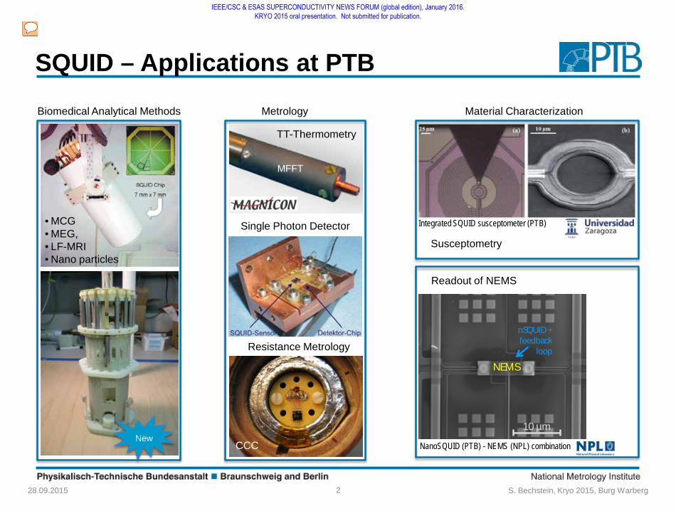
2-stage Readout
28.09.2015 7 S. Bechstein, Kryo 2015, Burg Warberg
SQUID series array
IEEE/CSC & ESAS SUPERCONDUCTIVITY NEWS FORUM (global edition), January 2016. KRYO 2015 oral presentation. Not submitted for publication.
Presenter
Presentation Notes
The best known SCS types consist of at least 16 single SQUIDs connected in series – which leads to the name ‘SQUID Series Array’ or SSA. The array acts as a single SQUID with enlarged output voltage.The signal, generated in the frontend SQUID, induces a current in the input coil of the SSA, and therefore a flux trough the input coil of the array. The output voltage of the array is then amplified by the room temperature electronics. (The feedback circuitry operates in the same way as described before.)

Demands for High Energy Resolution
28.09.2015 8 S. Bechstein, Kryo 2015, Burg Warberg
SΦ≈ 2L*16kBT*(LC)1/2
• efficiency ~ coupling or filling factor
small dimensions lower SQUID inductance + junction capacitance
• high energy resolution low and ultra-low temperatures
• high dynamic range
• high tolerance against applied magnetic field
ε = SΦ/(2L)
IEEE/CSC & ESAS SUPERCONDUCTIVITY NEWS FORUM (global edition), January 2016. KRYO 2015 oral presentation. Not submitted for publication.
Presenter
Presentation Notes
SQUIDs are extremely sensitive devices to detect changes in the magnetic field. The energy resolution depends on the magnetic flux noise and the SQUID inductance. The flux noise in turn depends on the inductance of the SQUID loop, the capacitance of the junctions, and the temperature, as well. Often, a high coupling or filling factor is needed for high efficiency. These are all reasons to shrink the size of the device. That means, one should develop SQUIDs rather with nano-sized junctions and nano- or micro-sized SQUID loops. In the last decade, a large number of working groups all over the world has developed nanoSQUIDs by using different technologies – partly with amazing results regarding the efficiency, or regarding the tolerated magnetic excitation field. But, most of these devices are not really convenient to handle, and some of them are not stable long term.
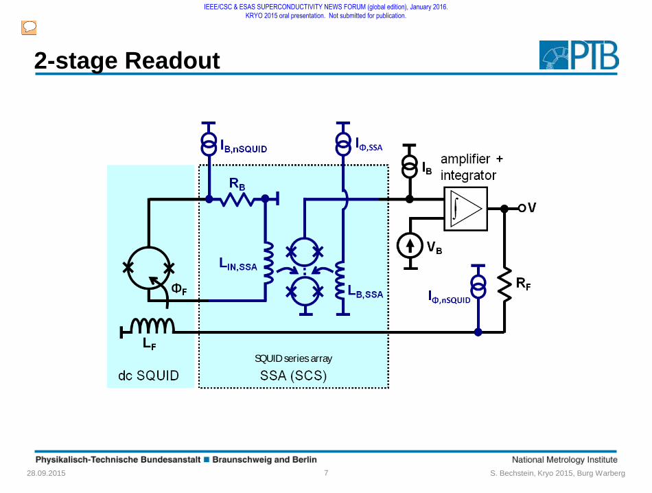
Josephson junctions: Intrinsically shunted SNS Junctions with HfTi Nominal lateral size: ca. 200nm x 200nm (180nm/220nm/240nm/260nm) Nominal barrier thickness: 30nm Distance between JJs: ≤ 1µm Design: PTB Berlin Fabrication: PTB Braunschweig SQUID Sensors: § SQUID gradiometers § SQUID current sensors Complements: § feedback § rf filter § 3 (4) different transformers
Nb/HfTi/Nb-NanoSQUIDs
28.09.2015 9 S. Bechstein, Kryo 2015, Burg Warberg
Chip 3mm x 3mm
nSQUID with transformers
IEEE/CSC & ESAS SUPERCONDUCTIVITY NEWS FORUM (global edition), January 2016. KRYO 2015 oral presentation. Not submitted for publication.
Presenter
Presentation Notes
That is the reason why PTB has started with a new family of micro- and nano-sized SQUID gradiometers which are made of a trilayer - with niobium as superconductor and HfTi as barrier. HfTi is a normal conductor which enables self-shunted junctions. That means there is no longer the need to integrate shunt resistors in the design. And thus, it enables a SQUID design with very small SQUID loops. PTB Braunschweig has developed a new technology based on electron beam lithography and a chemical mechanical polishing process (CMP), which enables junction sizes down to a few ten nm. Based on this new junction technology, PTB Berlin has developed several types of nano- and micro-sized SQUIDs. In general, these are SQUID series or parallel gradiometers, or SQUID current sensors. Each device is completed with a feedback circuitry, with rf filters to enhance the robustness, and with transformers, which are needed for sufficient coupling for feedback and working point adjustment into such small SQUID loops. The chip size is PTB’s standard chip size of about 3 mm x 3 mm. The soldering pads are located on the left-hand side, the rf filters (blue squares), too, whereas the SQUID sensor and the transformers are located on the lower right-hand corner.

Device Family
28.09.2015 10 S. Bechstein, Kryo 2015, Burg Warberg
nSQUID parallel gradiometer nSQUID current sensor µSQUID series gradiometer nSQUID series gradiometer
unpublished
S. Bechstein et al., „HfTi-nanoSQUID gradiometers with high linearity,“ Applied Physics Letters 106, 072601 (2015); doi: 10.1063/1.4909523
(a) (b) (c) (d)
IEEE/CSC & ESAS SUPERCONDUCTIVITY NEWS FORUM (global edition), January 2016. KRYO 2015 oral presentation. Not submitted for publication.
Presenter
Presentation Notes
Several types of nano and microSQUIDs are designed:(a) nanoSQUID parallel gradiometer(b) nanoSQUID series gradiometer(c) microSQUID series gradiometer with parts of a transformer(d) nanoSQUID current sensor.The equivalent schemes including the transformer are depicted below each SQUID design.(The transformers GCT and C7T are discussed in the next slide.)
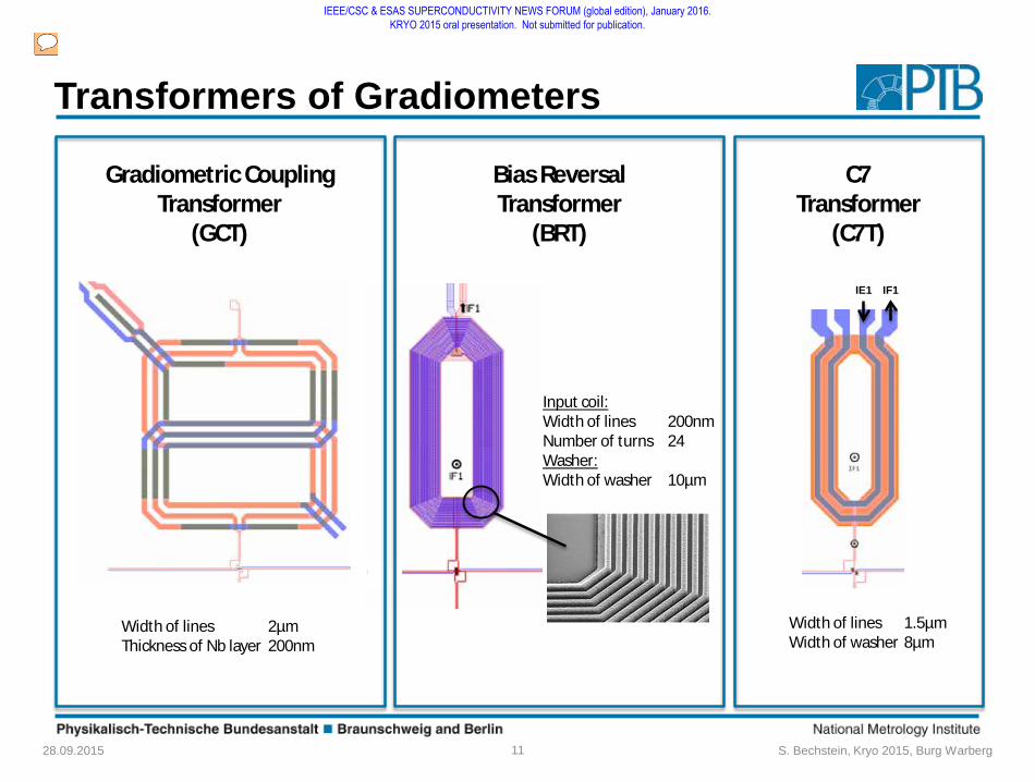
Transformers of Gradiometers
28.09.2015 11 S. Bechstein, Kryo 2015, Burg Warberg
C7 Transformer
(C7T)
IF1 IE1
Width of lines 1.5µm Width of washer 8µm
Bias Reversal Transformer
(BRT)
Input coil: Width of lines 200nm Number of turns 24 Washer: Width of washer 10µm
Gradiometric Coupling Transformer
(GCT)
Width of lines 2µm Thickness of Nb layer 200nm
IEEE/CSC & ESAS SUPERCONDUCTIVITY NEWS FORUM (global edition), January 2016. KRYO 2015 oral presentation. Not submitted for publication.
Presenter
Presentation Notes
The SQUID gradiometers are combined with different transformers designed for different purposes. Three types are available: • The first one is a Gradiometric Coupling Transformer (GCT) with both a gradiometric input and a gradiometric output coil in shape of an eight and with less niobium material than in the traditional washer structure.• The second one, the Bias Reversal Transformer (BRT) is a washer-type transformer intended to be used for bias reversal with its 24 turns of the input coil.• The third is a washer-type transformer, too, with both a feedback and an excitation coil. This transformer was originally developed for PTBs microsusceptometers (C7T).

Fabrication
28.09.2015 12 S. Bechstein, Kryo 2015, Burg Warberg
§ Clean room center Braunschweig § Electron beam lithography § Chemical mechanical polishing process (CMP) § Supporting structures consisting of Nb1 and HfTi integrated in design
§ homogeneous polished junctions
§ negligible small changes of Ic across the wafer area
§ protecting isolation @ bridges (e.g. filters)
high rate of yield
Clean room center (PTB Braunschweig).
IEEE/CSC & ESAS SUPERCONDUCTIVITY NEWS FORUM (global edition), January 2016. KRYO 2015 oral presentation. Not submitted for publication.
Presenter
Presentation Notes
Supporting structures are islands which are spread across the waver. They consist of two layers - the first niobium and the HfTi-layer, and support even wear across the waver during the chemical mechanical polishing (CMP) process. Thus, the junctions are more homogeneously polished which is essential for a reliable and reproducible SQUID fabrication: Since we use these supporting structures, the yield is excellent.

Inductance and Flux Noise
28.09.2015 13 S. Bechstein, Kryo 2015, Burg Warberg
Magnetic flux noise @ 20kHz … 50kHz
3 types of transformers
magnetic flux noise independent on type of transformer 110 nΦ0/√Hz achievable
Noise spectra
Setup: 2-stage configuration with SSA, FLL mode
IEEE/CSC & ESAS SUPERCONDUCTIVITY NEWS FORUM (global edition), January 2016. KRYO 2015 oral presentation. Not submitted for publication.
Presenter
Presentation Notes
The magnetic flux noise of the SQUIDs is always of substantial interest. In the diagram on the left-hand side, the flux noise measured in the white frequency region is depicted versus the measured SQUID inductance. The dark and light blue colored data points are obtained from two different wafers. It was found, that the white frequency noise of the parallel gradiometers is the lowest, as expected. It is about 115 nΦ0/√Hz. The white noise of the series gradiometers is about 200 nΦ0/√Hz. Here, the 12 data points represent 12 devices equipped with 3 different transformers. From these measurements we conclude, that the flux noise is independent on the type of transformer.Typical noise spectra of our nanoSQUID gradiometers look like depicted in the diagramm on the right-hand side: In the white frequency region, the flux noise level is about 200 nΦ0/√Hz (for the series gradiometer), or about 115 nΦ0/√Hz (in case of a parallel gradiometer with its lower inductance), respectively. In the lower frequency region, the level of flux noise is relatively high, thus the 1/f-corner is about 1 kHz. This behavior was already reported from other nanoSQUID groups, thus it isn’t specific to our devices.
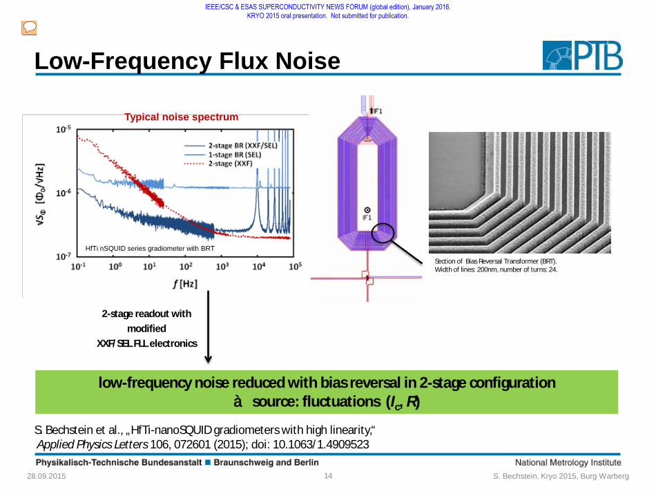
Low-Frequency Flux Noise
28.09.2015 14 S. Bechstein, Kryo 2015, Burg Warberg
2-stage readout with modified
XXF/SEL FLL electronics
Typical noise spectrum
low-frequency noise reduced with bias reversal in 2-stage configuration à source: fluctuations (Ic, R)
HfTi nSQUID series gradiometer with BRT
Section of Bias Reversal Transformer (BRT). Width of lines: 200nm, number of turns: 24.
S. Bechstein et al., „HfTi-nanoSQUID gradiometers with high linearity,“ Applied Physics Letters 106, 072601 (2015); doi: 10.1063/1.4909523
IEEE/CSC & ESAS SUPERCONDUCTIVITY NEWS FORUM (global edition), January 2016. KRYO 2015 oral presentation. Not submitted for publication.
Presenter
Presentation Notes
In order to investigate this unfavorable behavior, one of the nanoSQUID designs was equipped with a special transformer (BRT) which increases the current sensitivity to a level compatible with the maximum current of the SEL-type FLL electronics. (That is a commercially available electronic with bias reversal function.) In order to enable low noise measurements in the white noise range as well in the 1/f noise regime, an XXF-type electronics was combined with a modified SEL-type electronics in a common housing. In this special setup, the XXF-electronics provides the dc bias of the SSA and allows the readout in a two-stage configuration nanoSQUID/SSA. In addition, the modified SEL-electronics enables the dc and ac bias of the nanoSQUID. Using this setup, it was found, that for bias reversal frequencies between 1 kHz and 10 kHz, the noise in the lower frequency range is considerably reduced (dark blue data). This demonstrates the critical current or resistance fluctuations cause substantial contribution to the low-frequency flux noise.

Susceptometer Application
28.09.2015 15 S. Bechstein, Kryo 2015, Burg Warberg
HfTi-nanoSQUID gradiometers with GCT: linear (a) and nonlinear (b) part very low
suitable for susceptometer applications J
Measurement setup:
nSQUID locked in FLL mode (2-stage configuration)
linear increased/decreased
excitation field 0 < |Bp| ≤ |Bmax|
output signal
fit: polynomial of 6th degree
ΦLIN ΦNL
Setup: 2-stage configuration with SSA, FLL mode
Improved design: Bmax, GCT ≈ 15mT
IEEE/CSC & ESAS SUPERCONDUCTIVITY NEWS FORUM (global edition), January 2016. KRYO 2015 oral presentation. Not submitted for publication.
Presenter
Presentation Notes
For most of the applications, the linearity of the measuring system is of considerable interest - in addition to the flux noise.If a SQUID gradiometer is exposed to a magnetic excitation field, the output voltage of an empty device should be ideally zero, but in practice as small and linear as possible. In these two figures, the output voltage is converted into flux and depicted versus the applied magnetic field. In the diagram in the middle of the slide, the whole output signal is shown, in the diagram on the right-hand side, the nonlinear part thereof. Both figures show the data of several SQUID types in combination with different transformers. All these data are shown in black, whereas the bunch of colored data represents the HfTi-nanoSQUID series or parallel gradiometers which are combined with gradiometric coupling transformers.From both figures, one can conclude, that the output signal converted into flux, is dominated by the linear part, which represents the residual area of the gradiometric design. It was found, that if a HfTi-nanoSQUID series or parallel gradiometer is combined with a gradiometric coupling transformer (depicted by the bunch of colored lines), the linear as well as the nonlinear part of the output signal are very low - due to the fully gradiometric design including gradiometric transformers and the small junction size.Thus, these devices should be well suited for susceptometer applications.

NEMS Application
28.09.2015 16 S. Bechstein, Kryo 2015, Burg Warberg
Voltage across the nanoSQUID series gradiometer versus magnetic flux
(perpendicular to the SQUID loop).
suitable for NEMS readout J
Maximum voltage swing of a nanoSQUID series gradiometer with C7-transformer
versus dc magnetic field.
C7-transformer
BNEMS,dc
Setup: 1-stage configuration, AMP mode
B║
B┴
IEEE/CSC & ESAS SUPERCONDUCTIVITY NEWS FORUM (global edition), January 2016. KRYO 2015 oral presentation. Not submitted for publication.
Presenter
Presentation Notes
Another application is the readout of nanoelectromechanical systems (NEMS).In this case, the field tolerance against an in-plane dc magnetic field is rather of interest. Measurements of the maximum voltage swing and the corresponding bias current as well, show a typical Fraunhofer pattern with a first minimum at about 80 mT. These measurements as well as... (next slide)

NEMS Application
28.09.2015 17 S. Bechstein, Kryo 2015, Burg Warberg
Section of a combination of a nanoSQUID series gradiometer with GCT and NEMS
(cooperation with NPL).
NEMS
nSQUID + feedback
loop
transformer
InSQUID,bias INEMS,ac
10 µm
BNEMS,dc
IF
suitable for NEMS readout J
Voltage of a nanoSQUID series gradiometer with GCT/SSA combination
versus magnetic flux.
Setup: 2-stage configuration with SSA, AMP mode
IEEE/CSC & ESAS SUPERCONDUCTIVITY NEWS FORUM (global edition), January 2016. KRYO 2015 oral presentation. Not submitted for publication.
Presenter
Presentation Notes
... two-stage measurements as shown in the diagram, indicate the suitability of our new HfTi-nanoSQUIDs in dc magnetic fields of at least a few 10 mT up to a few hundred mT – depending on the type of transformer and the operation mode.The photo on the right-hand side shows a first attempt of a combination of a HfTi-nanoSQUID series gradiometer and a nanoelectomechanical system (NEMS). The double clamped nano-beam was produced at NPL using focused ion beam (FIB) for milling, and positioned above the nanoSQUID using a sharpened carbon fiber connected to an in chamber micromanipulator.Just now, this device is ready for measurements.
Milestone: new family of HfTi-nanoSQUID sensors
§ technology well established
§ complex sensors gradiometers and current sensors with transformers, feedback circuitry, rf filters
§ low level of nonlinearity susceptometer application
§ field tolerance of at least a few mT up to a few 100mT NEMS readout depending on operation and type of transformer
Outlook:
§ design § further improvement of field tolerance, smaller structures (transformers) § further adaption to each application (further specialization)
§ measurements § susceptometer measurements together with partners
(nano particles, molecules, single spin detection) § NEMS readout
Summary / Outlook
28.09.2015 18 S. Bechstein, Kryo 2015, Burg Warberg
IEEE/CSC & ESAS SUPERCONDUCTIVITY NEWS FORUM (global edition), January 2016. KRYO 2015 oral presentation. Not submitted for publication.

Physikalisch-Technische Bundesanstalt Braunschweig und Berlin Abbestr. 2-12 10587 Berlin Sylke Bechstein Phon: 030 3481-7426 E-Mail: [email protected] www.ptb.de
Status: 06.10.2015
Thank you: Corinna Neubauer Frank Ruede Lars Schikowski Kathrin Störr
This work was partly supported by the DFG under Grant No. SCHU1950/5-1 and within the European Metrology Research Programme EMRP ‘MetNEMS’ NEW-08, which is jointly funded by the participating countries within EURAMET and the European Union.
IEEE/CSC & ESAS SUPERCONDUCTIVITY NEWS FORUM (global edition), January 2016. KRYO 2015 oral presentation. Not submitted for publication.