hfss ppt
76
“HFSS (HIGH FREQUENCY STRUCTURAL SIMULATOR ) TUTORIAL ” BY Dr. Ravi Kumar Gangwar Asst. Prof. Department of Electronics Engineering I.S.M.Dhanbad, Jharkhand 1
-
Upload
shailjachaudhary -
Category
Documents
-
view
2 -
download
0
description
to learn usage of HFSS for strip fed as well as co axial antenna simulation
Transcript of hfss ppt

“HFSS (HIGH FREQUENCY STRUCTURAL SIMULATOR ) TUTORIAL ”
BY Dr. Ravi Kumar Gangwar
Asst. Prof. Department of Electronics Engineering
I.S.M.Dhanbad, Jharkhand1

Flow Of Presentation Introduction Of HFSS.Flow Chart for Design in HFSS.Algorithm for Design in HFSS.Design Example For HFSS.
DRA(Dielectric Resonator Antenna) with coaxial feed. DRA with microstrip feed.

What is HFSS ?HFSS is an interactive software package for
calculating the electromagnetic behavior of a structure.
Using HFSS we can compute:-Basic electromagnetic field quantities and, for open
boundary problems, radiated near and far fields.Characteristic port impedances and propagation
constants.Generalized S-parameters and S-parameters
renormalized to specific port impedances.

How to proceed for a project in HFSS?
We are expected to draw the structure, specify material characteristics for each object, and identify ports and special surface characteristics. HFSS then generates the necessary field solutions and associated port characteristics and S-parameters.
As we set up the problem, HFSS allows us to specify whether to solve the problem at one specific frequency or at several frequencies within a range.

System Requirement for HFSSoSupported Platforms:-
• Windows XP Professional (32-bit and 64-bit)
• Windows Server 2003 (32-bit and 64-bit)
• Windows Vista Service Pack 1 (32-bit and 64-bit)
oMinimum System Requirements:-
•Processor: All fully compatible 686 (or later) instruction set processors, 500 MHz•Hard Drive Space (for HFSS software): 200 MB•RAM: 512 MB

Flow Chart for Design a Project in HFSS
Start
Design geometrical structure of our project and assign related material for each shaped element according to our project
Assign boundary, excitation (lumped port, wave port)
Go for Analysis setup(Assign the frequency sweep range and solution frequency)
Run the designed structure and analyze the results
End

Algorithm for Design a Project in HFSS 1. Start.
2. Open HFSS software .
3. Insert Geometrical Project design.
4. Assign material for each element of the project.
5. Assign radiation boundary for the Designed structure .
6. Give the excitation(lumped port and wave port) to the designed structure.
7. Go for the analysis setup (assign frequency sweep range and solution frequency).
8. Run the project and analyzed the results.
9. Stop.
Design Example For HFSS
Open the software :-
It will open the new window which looks like this.
o DRA(dielectric Resonator Antenna)

Elements of HFSS Window:-

Open new project:-When we will open the software it will automatically open a new project window, just rename as per our requirement(rdra) .
Save the project:- Go to file click on ‘save as ‘ it will save the project where ever we want depend upon our requirement .

Set the drawing unit before we start design
• Go to modeler in menu and click on units it will one unit window select our required unit normally we select ‘mm’

Take ground plane:-
• For taking ground plane select Draw Box from the toolbar, if it is not available in toolbar than bring cursor to toolbar and by right click on mouse at anywhere in toolbar it will give us list in that click tick on 3D Draw solid. Or go to menu in that click on draw and then click box.
• Our aim is draw 50x50x3 ground plane .• We want it should look in center.

Ground plane of 50x50x3

Change the name of box.For that go to history tree in that double click on box1 and change the name as ground

change the dimension of box as 50x50x3For that go to the history tree and expand ground in that double click on create box .Now we will get one small window in that change position ,x size , y size and z size as shown in below.

Assign the material for ground.For assigning the material right click on grnd and select ‘pec’ material.

Draw rectangular DRA with dimension of 10x10x10(Length x Width x Height).
Do same as ground for rename and dimensions

Assign material for rdra.For that repeat same but select rdra from history tree and select add new material (dielectric constant is 20).
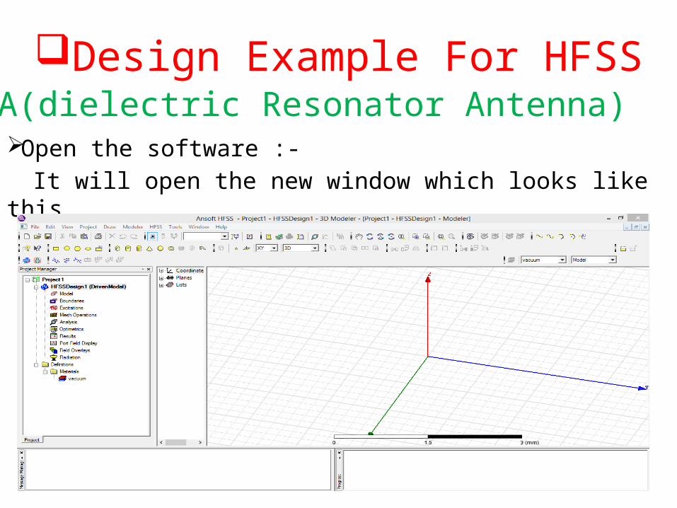
Designing of Coaxial probe for feeding Rectangular DRA.
• For designing of Coaxial feed first we will calculate Coaxial parameter.
• Inner Diameter-D1
Outer Diameter-D2
Dielectric material- Teflon
Conductor material- Pec

Calculation of Coaxial Probe parameter:-
• http://www1.sphere.ne.jp/i-lab/ilab/tool/cx_line_e.htm
Go to the below link and enter the data as impedance50 Ω and dielectric material constant 2.1(teflon).

Designing of dielectric part for coaxial probe:-Select cylinder dimension of 2 mm radius with 3 mm heightand subtract with ground which will create hole of taken cylinder , now again take same dimension cylinder.

How to do subtraction from one shape to other shape:-Select both shape from the history tree and perform subtract operation .

Designing of conductor part for coaxial probe:-Select one cylinder dimension of 0.6 mm radius and7 mm height and subtract from dielectric part whichwill create hole of required dimension ,now again select one cylinder of the same dimension.

Designing of radiation box:-Take one box dimension of 50 mm x 50 mm x 50 mm which will a vacuum .

Radiation box :-

Cont…

Assigning of port for excitation of coaxial probe:- Take one circle to cover the coaxial feed point so that we can assign the port.

Cont…Assign wave port as excitation, select circle form history tree and right click on that select assign excitation in that again select Wave port .

Cont…Now we need to define integration line as new line manually we need to define the line from center to circumference.

Cont…After define integration line, it will be defined which is showing in below figure.

Cont…It will give the impedance of 50 Ω.

Cont…
Wave port will looks like that after assigning.

Analysis setup:-Go to HFSS and click on that and select analysis setup in that click on add solution setup.

Cont...After clicking on add solution setup we will get above window in that we need to specify following:-
Maximum number of passes- 5 to 20(depends upon how much fine result we want) Maximum delta S- 0.02

Cont…

Add frequency sweep:-Go to HFSS and click on that and select analysis setup in that click on add frequency sweep.

Cont…
After getting the above window we need to do following changes depends upon our requirement :-
•Sweep name – sweep•Sweep type- fast•Type – linear count

Cont…

Validation check:-Click on validate.

Analysis of structure:-Click on analysis all.

Result:-Go to HFSS and click on results tab.

S11 versus frequency curve :-It will show the return loss versus frequency curve.

Calculation of Resonant frequency and Bandwidth:-
Bandwidth= (m2-m1) HzResonant frequency=m3 Hz

Calculation of far field pattern:-•For far field calculation we need to define radiation .•Go to project tree select radiation and right click on that than we will get some option in that select insert far field setup , and select infinite sphere.

Cont…

3-D radiation pattern :-For getting the 3-D radiation patter , go to HFSS then select results then select create far field report than select 3-D polar plot.

Designing of rectangular DRA with microstrip feeding
Select ground of given parameter as box from the tool bar
Selection of ground

Cont…Ground material will be copper or pec.

Substrate selection Substrate is going to keep on ground it can be selectdepend upon market availability, here we are keeping0.8mm thick.

Cont…For substrate we will FR4 material, which dielectric constant is 4.4

Rectangular DRA
Rectangular DRA dimension is 10mmx10mmx10mm is selected and kept on substrate .

Cont…Here we are choosing dielectric constant of 20 for Rectangular DRA.

Microstrip feed lineFor the calculation of width of microstrip line we will follow below slide.

How to calculate parameter of microstrip line.
We know that Substrate thickness (h)=0.8mmSubstrate dielectric constant(Ɛr)=4.4Microstrip line thickness=0.035mmResonant frequency=4.5 GHzImpedance = 50 Ω
By substituting these value in online calculator we can get the width of microstrip line.

Designing of Microstrip feed for Rectangular DRA.

Calculation of parameter :-http://www1.sphere.ne.jp/i-lab/ilab/tool/ms_line_e.htm

Cont…Microstrip line material will be same as groundand thickness will be also same as ground.

Designing of feed point for microstrip line:-
Feed point will be design by one rectangular sheetwhich dimension will be decided by below formula.

Dimension of sheet

Cont…Sheet will be used for assigning of wave port.

Assigning of wave port:-• Assign wave port as excitation, select sheet in that
rectangular form history tree and right click on that select assign excitation in that again select Wave port .
• Do the same as coaxial probe feed.

Cont…It will give the 50 Ω impedance.

Radiation box:-Radiation box dimension will be 50mmx50mmx50mm.

Cont…This radiation box will be assign as radiation boundary.

Radiation boundary:-

Analysis setup:-Go to HFSS and click on that and select analysis setup in that click on add solution setup.

Cont...After clicking on add solution setup we will get above window in that we need to specify following:-
Maximum number of passes- 5 to 20(depends upon how much fine result we want) Maximum delta S- 0.02

Cont…

Add frequency sweep:-Go to HFSS and click on that and select analysis setup in that click on add frequency sweep.

Cont…
After getting the above window we need to do following changes depends upon our requirement :-
•Sweep name – sweep•Sweep type- fast•Type – linear count

Validation check:-Click on validate.

Analysis of structure:-Click on analysis all.

Result:-Go to HFSS and click on results tab.

Return loss versus frequency curve:-

Results Calculation
• Bandwidth =m2-m1=(4.7-4.4) GHz = 0.3 GHz• Resonant frequency=m3=4.5 GHz

Thank
you