Heating Effects in Nanoscale Devices - InTech - Open Science Open
30
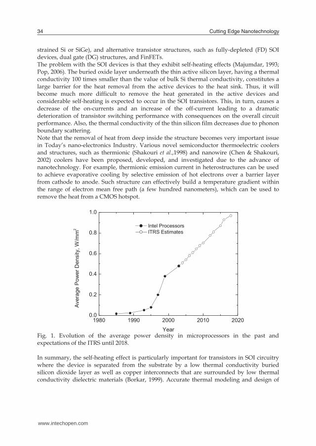
Heating Effects in Nanoscale Devices 33 X Heating Effects in Nanoscale Devices Dragica Vasileska 1 , Katerina Raleva 2 and Stephen M. Goodnick 1 1 Arizona State University, Tempe, AZ, 85287-5706, USA 2 University Sts Cyril and Methodius, Skopje, Macedonia 1. Introduction The ever increasing demand for faster microprocessors and the continuous trend to pack more transistors on a single chip has resulted in an unprecedented level of power dissipation, and therefore higher temperatures at the chip level. Thermal phenomena are not directly responsible for the electrical functionality and performance of semiconductor devices, but adversely affect their reliability. Four major thermally-induced reliability concerns for transistors are: (1) degradation of device thermal characteristics due to heating effects, (2) failure due to the electrostatic discharge phenomenon, (3) stresses due to different rates of thermal expansion of transistor constituents, and (4) failure of metallic interconnects due to diffusion or flow of atoms along a metal interconnect in the presence of a bias current, known as the electromigration phenomenon. Self-heating of the device and interconnects reduces electron mobility and results in a poor or, at best, non-optimal, performance of these devices and structures. Fig. 1 shows the trend of the average power density for high-performance microprocessors according to the ITRS. No flattening or slower decelerated increase will occur after the introduction of the Silicon on Insulator (SOI) technology. It should be noted that the power density shown in Fig. 1 is the average power density, i.e. the total chip power divided by the chip area. In logic circuits, such as microprocessors, the power is non-uniformly distributed. There are portions of the chip of quite low power dissipation (memory blocks) and, on the other hand, portions running at full speed with high activity factors where the power density can easily be more than a magnitude higher than the average chip power density from Fig. 1. The latter portions will create hot spots with quite high local temperature. The power density in the active transistor region (essentially the channel region underneath the gate) is again much higher than the average power density in a hot spot when the transistor is in the on-state. Thus, the treatment of self-heating and the realistic estimation of the power density is quite a complex problem. Sometime within the next five years, traditional CMOS technology is expected to reach limits of scaling. As channel lengths shrink below 22 nm, complex channel profiles are required to achieve desired threshold voltages and to alleviate the short-channel effects. To fabricate devices beyond current scaling limits, Integrated Circuits (IC) companies are simultaneously pushing planar, bulk silicon CMOS design while exploring alternative gate stack materials (high-k dielectrics and metal gates), band engineering methods (using 3 www.intechopen.com
Transcript of Heating Effects in Nanoscale Devices - InTech - Open Science Open

Heating Effects in Nanoscale Devices 33
Heating Effects in Nanoscale Devices
Dragica Vasileska, Katerina Raleva and Stephen M. Goodnick
X
Heating Effects in Nanoscale Devices
Dragica Vasileska1, Katerina Raleva2 and Stephen M. Goodnick1 1Arizona State University, Tempe, AZ, 85287-5706, USA
2University Sts Cyril and Methodius, Skopje, Macedonia
1. Introduction
The ever increasing demand for faster microprocessors and the continuous trend to pack more transistors on a single chip has resulted in an unprecedented level of power dissipation, and therefore higher temperatures at the chip level. Thermal phenomena are not directly responsible for the electrical functionality and performance of semiconductor devices, but adversely affect their reliability. Four major thermally-induced reliability concerns for transistors are: (1) degradation of device thermal characteristics due to heating effects, (2) failure due to the electrostatic discharge phenomenon, (3) stresses due to different rates of thermal expansion of transistor constituents, and (4) failure of metallic interconnects due to diffusion or flow of atoms along a metal interconnect in the presence of a bias current, known as the electromigration phenomenon. Self-heating of the device and interconnects reduces electron mobility and results in a poor or, at best, non-optimal, performance of these devices and structures. Fig. 1 shows the trend of the average power density for high-performance microprocessors according to the ITRS. No flattening or slower decelerated increase will occur after the introduction of the Silicon on Insulator (SOI) technology. It should be noted that the power density shown in Fig. 1 is the average power density, i.e. the total chip power divided by the chip area. In logic circuits, such as microprocessors, the power is non-uniformly distributed. There are portions of the chip of quite low power dissipation (memory blocks) and, on the other hand, portions running at full speed with high activity factors where the power density can easily be more than a magnitude higher than the average chip power density from Fig. 1. The latter portions will create hot spots with quite high local temperature. The power density in the active transistor region (essentially the channel region underneath the gate) is again much higher than the average power density in a hot spot when the transistor is in the on-state. Thus, the treatment of self-heating and the realistic estimation of the power density is quite a complex problem. Sometime within the next five years, traditional CMOS technology is expected to reach limits of scaling. As channel lengths shrink below 22 nm, complex channel profiles are required to achieve desired threshold voltages and to alleviate the short-channel effects. To fabricate devices beyond current scaling limits, Integrated Circuits (IC) companies are simultaneously pushing planar, bulk silicon CMOS design while exploring alternative gate stack materials (high-k dielectrics and metal gates), band engineering methods (using
3
www.intechopen.com
Cutting Edge Nanotechnology34
strained Si or SiGe), and alternative transistor structures, such as fully-depleted (FD) SOI devices, dual gate (DG) structures, and FinFETs. The problem with the SOI devices is that they exhibit self-heating effects (Majumdar, 1993; Pop, 2006). The buried oxide layer underneath the thin active silicon layer, having a thermal conductivity 100 times smaller than the value of bulk Si thermal conductivity, constitutes a large barrier for the heat removal from the active devices to the heat sink. Thus, it will become much more difficult to remove the heat generated in the active devices and considerable self-heating is expected to occur in the SOI transistors. This, in turn, causes a decrease of the on-currents and an increase of the off-current leading to a dramatic deterioration of transistor switching performance with consequences on the overall circuit performance. Also, the thermal conductivity of the thin silicon film decreases due to phonon boundary scattering. Note that the removal of heat from deep inside the structure becomes very important issue in Today’s nano-electronics Industry. Various novel semiconductor thermoelectric coolers and structures, such as thermionic (Shakouri et al.,1998) and nanowire (Chen & Shakouri, 2002) coolers have been proposed, developed, and investigated due to the advance of nanotechnology. For example, thermionic emission current in heterostructures can be used to achieve evaporative cooling by selective emission of hot electrons over a barrier layer from cathode to anode. Such structure can effectively build a temperature gradient within the range of electron mean free path (a few hundred nanometers), which can be used to remove the heat from a CMOS hotspot.
1980 1990 2000 2010 20200.0
0.2
0.4
0.6
0.8
1.0
Intel Processors ITRS Estimates
Aver
age
Pow
er D
ensi
ty, W
/mm
2
Year Fig. 1. Evolution of the average power density in microprocessors in the past and expectations of the ITRS until 2018. In summary, the self-heating effect is particularly important for transistors in SOI circuitry where the device is separated from the substrate by a low thermal conductivity buried silicon dioxide layer as well as copper interconnects that are surrounded by low thermal conductivity dielectric materials (Borkar, 1999). Accurate thermal modeling and design of
microelectronic devices and thin film structures at micro- and nanoscales poses a challenge to the thermal engineers who are less familiar with the basic concepts and ideas in sub-continuum heat transport.
2. Some General Aspects of Heat Conduction
The energy given up by the constituent particles such as atoms, molecules, or free electrons of the hotter regions of a body to those in cooler regions is called heat. Conduction is the mode of heat transfer in which energy exchange takes place in solids or in fluids in rest (i.e. no convection motion resulting from the displacement of the macroscopic portion of the medium) from the region of high temperature to the region of low temperature due to the presence of temperature gradient in the body. The heat flow can not be measured directly, but the concept has physical meaning because it is related to the measurable scalar quantity called temperature. Therefore, once the temperature distribution T(r,t) within a body is determined as a function of position and time, then the heat flow in the body is readily computed from the laws relating heat flow to the temperature gradient. The science of heat conduction is principally concerned with the determination of temperature distribution within solids. The basic law that gives the relationship between the heat flow and the temperature gradient, based on experimental observations, is generally named after the French mathematical physicist Joseph Fourier, who used it in his analytic theory of heat. For a homogeneous, isotropic solid (i.e. material in which thermal conductivity is independent of direction) the Fourier law is given in the form
2q(r, ) (r, ) /t T t W m (1)
where the temperature gradient is a vector normal to the isothermal surface, the heat flux vector q(r,t) represents heat flow per unit time, per unit area of the isothermal surface in the direction of the decreasing temperature, and is called the thermal conductivity of the material which is a positive, scalar quantity. Since the heat flux vector q(r,t) points in the direction of decreasing temperature, a minus sign is included in Eq. (1) to make the heat flow a positive quantity. When the heat flux is in W/m2 and the temperature gradient is in C/m, the thermal conductivity has the units W/(m C). Clearly, the heat flow rate for a given temperature gradient is directly proportional to the thermal conductivity of the material. Therefore, in the analysis of heat conduction, the thermal conductivity of the material is an important property, which controls the rate of heat flow in the medium. There is a wide difference in the thermal conductivities of various engineering materials. The highest value is given by pure metals and the lowest value by gases and vapors; the amorphous insulating materials and inorganic liquids have thermal conductivities that lie in between. Thermal conductivity also varies with temperature. For most pure metals it decreases with temperature, whereas for gases it increases with increasing temperature. At nanometer length scales, the familiar continuum Fourier law for heat conduction is expected to fail due to both classical and quantum size effects (Geppert, 1999; Zeng et al., 2003; Majumdar, 1993). The past two decades have seen increasing attention to thermal conductivity and heat conduction in nanostructures. Experimental methods for characterizing the thermal conductivity of thin films and nanowires have been developed
www.intechopen.com
Heating Effects in Nanoscale Devices 35
strained Si or SiGe), and alternative transistor structures, such as fully-depleted (FD) SOI devices, dual gate (DG) structures, and FinFETs. The problem with the SOI devices is that they exhibit self-heating effects (Majumdar, 1993; Pop, 2006). The buried oxide layer underneath the thin active silicon layer, having a thermal conductivity 100 times smaller than the value of bulk Si thermal conductivity, constitutes a large barrier for the heat removal from the active devices to the heat sink. Thus, it will become much more difficult to remove the heat generated in the active devices and considerable self-heating is expected to occur in the SOI transistors. This, in turn, causes a decrease of the on-currents and an increase of the off-current leading to a dramatic deterioration of transistor switching performance with consequences on the overall circuit performance. Also, the thermal conductivity of the thin silicon film decreases due to phonon boundary scattering. Note that the removal of heat from deep inside the structure becomes very important issue in Today’s nano-electronics Industry. Various novel semiconductor thermoelectric coolers and structures, such as thermionic (Shakouri et al.,1998) and nanowire (Chen & Shakouri, 2002) coolers have been proposed, developed, and investigated due to the advance of nanotechnology. For example, thermionic emission current in heterostructures can be used to achieve evaporative cooling by selective emission of hot electrons over a barrier layer from cathode to anode. Such structure can effectively build a temperature gradient within the range of electron mean free path (a few hundred nanometers), which can be used to remove the heat from a CMOS hotspot.
1980 1990 2000 2010 20200.0
0.2
0.4
0.6
0.8
1.0
Intel Processors ITRS Estimates
Aver
age
Pow
er D
ensi
ty, W
/mm
2
Year Fig. 1. Evolution of the average power density in microprocessors in the past and expectations of the ITRS until 2018. In summary, the self-heating effect is particularly important for transistors in SOI circuitry where the device is separated from the substrate by a low thermal conductivity buried silicon dioxide layer as well as copper interconnects that are surrounded by low thermal conductivity dielectric materials (Borkar, 1999). Accurate thermal modeling and design of
microelectronic devices and thin film structures at micro- and nanoscales poses a challenge to the thermal engineers who are less familiar with the basic concepts and ideas in sub-continuum heat transport.
2. Some General Aspects of Heat Conduction
The energy given up by the constituent particles such as atoms, molecules, or free electrons of the hotter regions of a body to those in cooler regions is called heat. Conduction is the mode of heat transfer in which energy exchange takes place in solids or in fluids in rest (i.e. no convection motion resulting from the displacement of the macroscopic portion of the medium) from the region of high temperature to the region of low temperature due to the presence of temperature gradient in the body. The heat flow can not be measured directly, but the concept has physical meaning because it is related to the measurable scalar quantity called temperature. Therefore, once the temperature distribution T(r,t) within a body is determined as a function of position and time, then the heat flow in the body is readily computed from the laws relating heat flow to the temperature gradient. The science of heat conduction is principally concerned with the determination of temperature distribution within solids. The basic law that gives the relationship between the heat flow and the temperature gradient, based on experimental observations, is generally named after the French mathematical physicist Joseph Fourier, who used it in his analytic theory of heat. For a homogeneous, isotropic solid (i.e. material in which thermal conductivity is independent of direction) the Fourier law is given in the form
2q(r, ) (r, ) /t T t W m (1)
where the temperature gradient is a vector normal to the isothermal surface, the heat flux vector q(r,t) represents heat flow per unit time, per unit area of the isothermal surface in the direction of the decreasing temperature, and is called the thermal conductivity of the material which is a positive, scalar quantity. Since the heat flux vector q(r,t) points in the direction of decreasing temperature, a minus sign is included in Eq. (1) to make the heat flow a positive quantity. When the heat flux is in W/m2 and the temperature gradient is in C/m, the thermal conductivity has the units W/(m C). Clearly, the heat flow rate for a given temperature gradient is directly proportional to the thermal conductivity of the material. Therefore, in the analysis of heat conduction, the thermal conductivity of the material is an important property, which controls the rate of heat flow in the medium. There is a wide difference in the thermal conductivities of various engineering materials. The highest value is given by pure metals and the lowest value by gases and vapors; the amorphous insulating materials and inorganic liquids have thermal conductivities that lie in between. Thermal conductivity also varies with temperature. For most pure metals it decreases with temperature, whereas for gases it increases with increasing temperature. At nanometer length scales, the familiar continuum Fourier law for heat conduction is expected to fail due to both classical and quantum size effects (Geppert, 1999; Zeng et al., 2003; Majumdar, 1993). The past two decades have seen increasing attention to thermal conductivity and heat conduction in nanostructures. Experimental methods for characterizing the thermal conductivity of thin films and nanowires have been developed
www.intechopen.com
Cutting Edge Nanotechnology36
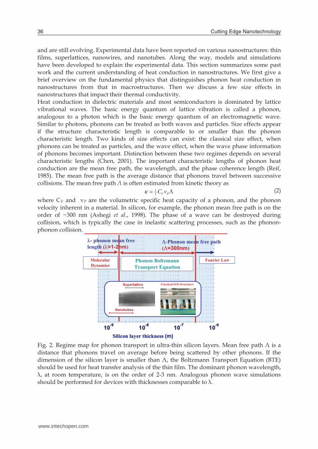
and are still evolving. Experimental data have been reported on various nanostructures: thin films, superlattices, nanowires, and nanotubes. Along the way, models and simulations have been developed to explain the experimental data. This section summarizes some past work and the current understanding of heat conduction in nanostructures. We first give a brief overview on the fundamental physics that distinguishes phonon heat conduction in nanostructures from that in macrostructures. Then we discuss a few size effects in nanostructures that impact their thermal conductivity. Heat conduction in dielectric materials and most semiconductors is dominated by lattice vibrational waves. The basic energy quantum of lattice vibration is called a phonon, analogous to a photon which is the basic energy quantum of an electromagnetic wave. Similar to photons, phonons can be treated as both waves and particles. Size effects appear if the structure characteristic length is comparable to or smaller than the phonon characteristic length. Two kinds of size effects can exist: the classical size effect, when phonons can be treated as particles, and the wave effect, when the wave phase information of phonons becomes important. Distinction between these two regimes depends on several characteristic lengths (Chen, 2001). The important characteristic lengths of phonon heat conduction are the mean free path, the wavelength, and the phase coherence length (Reif, 1985). The mean free path is the average distance that phonons travel between successive collisions. The mean free path Λ is often estimated from kinetic theory as 1
3 V PC v (2) where CV and vP are the volumetric specific heat capacity of a phonon, and the phonon velocity inherent in a material. In silicon, for example, the phonon mean free path is on the order of ~300 nm (Ashegi et al., 1998). The phase of a wave can be destroyed during collision, which is typically the case in inelastic scattering processes, such as the phonon-phonon collision.
10-9 10-8 10-7 10-6
Silicon layer thickness (m)
MolecularDynamics
Phonon Boltzmann Transport Equation
Fourier Law
Classical SOI StructuresSuperlattice
Nanotubes
10-9 10-8 10-7 10-6
Silicon layer thickness (m)
MolecularDynamics
Phonon Boltzmann Transport Equation
Fourier Law
Classical SOI StructuresSuperlattice
Nanotubes
-Phonon mean free path(=300nm)
- phonon mean freelength (=1-2nm)
Fig. 2. Regime map for phonon transport in ultra-thin silicon layers. Mean free path Λ is a distance that phonons travel on average before being scattered by other phonons. If the dimension of the silicon layer is smaller than Λ, the Boltzmann Transport Equation (BTE) should be used for heat transfer analysis of the thin film. The dominant phonon wavelength, λ, at room temperature, is on the order of 2-3 nm. Analogous phonon wave simulations should be performed for devices with thicknesses comparable to λ.
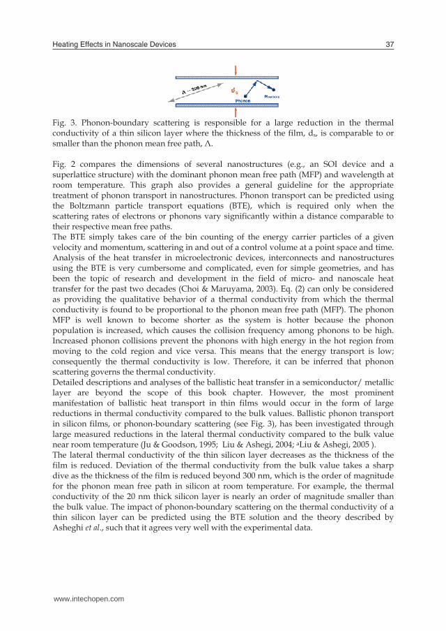
Fig. 3. Phonon-boundary scattering is responsible for a large reduction in the thermal conductivity of a thin silicon layer where the thickness of the film, ds, is comparable to or smaller than the phonon mean free path, Λ. Fig. 2 compares the dimensions of several nanostructures (e.g., an SOI device and a superlattice structure) with the dominant phonon mean free path (MFP) and wavelength at room temperature. This graph also provides a general guideline for the appropriate treatment of phonon transport in nanostructures. Phonon transport can be predicted using the Boltzmann particle transport equations (BTE), which is required only when the scattering rates of electrons or phonons vary significantly within a distance comparable to their respective mean free paths. The BTE simply takes care of the bin counting of the energy carrier particles of a given velocity and momentum, scattering in and out of a control volume at a point space and time. Analysis of the heat transfer in microelectronic devices, interconnects and nanostructures using the BTE is very cumbersome and complicated, even for simple geometries, and has been the topic of research and development in the field of micro- and nanoscale heat transfer for the past two decades (Choi & Maruyama, 2003). Eq. (2) can only be considered as providing the qualitative behavior of a thermal conductivity from which the thermal conductivity is found to be proportional to the phonon mean free path (MFP). The phonon MFP is well known to become shorter as the system is hotter because the phonon population is increased, which causes the collision frequency among phonons to be high. Increased phonon collisions prevent the phonons with high energy in the hot region from moving to the cold region and vice versa. This means that the energy transport is low; consequently the thermal conductivity is low. Therefore, it can be inferred that phonon scattering governs the thermal conductivity. Detailed descriptions and analyses of the ballistic heat transfer in a semiconductor/ metallic layer are beyond the scope of this book chapter. However, the most prominent manifestation of ballistic heat transport in thin films would occur in the form of large reductions in thermal conductivity compared to the bulk values. Ballistic phonon transport in silicon films, or phonon-boundary scattering (see Fig. 3), has been investigated through large measured reductions in the lateral thermal conductivity compared to the bulk value near room temperature (Ju & Goodson, 1995; Liu & Ashegi, 2004; aLiu & Ashegi, 2005 ). The lateral thermal conductivity of the thin silicon layer decreases as the thickness of the film is reduced. Deviation of the thermal conductivity from the bulk value takes a sharp dive as the thickness of the film is reduced beyond 300 nm, which is the order of magnitude for the phonon mean free path in silicon at room temperature. For example, the thermal conductivity of the 20 nm thick silicon layer is nearly an order of magnitude smaller than the bulk value. The impact of phonon-boundary scattering on the thermal conductivity of a thin silicon layer can be predicted using the BTE solution and the theory described by Asheghi et al., such that it agrees very well with the experimental data.
www.intechopen.com
Heating Effects in Nanoscale Devices 37
and are still evolving. Experimental data have been reported on various nanostructures: thin films, superlattices, nanowires, and nanotubes. Along the way, models and simulations have been developed to explain the experimental data. This section summarizes some past work and the current understanding of heat conduction in nanostructures. We first give a brief overview on the fundamental physics that distinguishes phonon heat conduction in nanostructures from that in macrostructures. Then we discuss a few size effects in nanostructures that impact their thermal conductivity. Heat conduction in dielectric materials and most semiconductors is dominated by lattice vibrational waves. The basic energy quantum of lattice vibration is called a phonon, analogous to a photon which is the basic energy quantum of an electromagnetic wave. Similar to photons, phonons can be treated as both waves and particles. Size effects appear if the structure characteristic length is comparable to or smaller than the phonon characteristic length. Two kinds of size effects can exist: the classical size effect, when phonons can be treated as particles, and the wave effect, when the wave phase information of phonons becomes important. Distinction between these two regimes depends on several characteristic lengths (Chen, 2001). The important characteristic lengths of phonon heat conduction are the mean free path, the wavelength, and the phase coherence length (Reif, 1985). The mean free path is the average distance that phonons travel between successive collisions. The mean free path Λ is often estimated from kinetic theory as 1
3 V PC v (2) where CV and vP are the volumetric specific heat capacity of a phonon, and the phonon velocity inherent in a material. In silicon, for example, the phonon mean free path is on the order of ~300 nm (Ashegi et al., 1998). The phase of a wave can be destroyed during collision, which is typically the case in inelastic scattering processes, such as the phonon-phonon collision.
10-9 10-8 10-7 10-6
Silicon layer thickness (m)
MolecularDynamics
Phonon Boltzmann Transport Equation
Fourier Law
Classical SOI StructuresSuperlattice
Nanotubes
10-9 10-8 10-7 10-6
Silicon layer thickness (m)
MolecularDynamics
Phonon Boltzmann Transport Equation
Fourier Law
Classical SOI StructuresSuperlattice
Nanotubes
-Phonon mean free path(=300nm)
- phonon mean freelength (=1-2nm)
Fig. 2. Regime map for phonon transport in ultra-thin silicon layers. Mean free path Λ is a distance that phonons travel on average before being scattered by other phonons. If the dimension of the silicon layer is smaller than Λ, the Boltzmann Transport Equation (BTE) should be used for heat transfer analysis of the thin film. The dominant phonon wavelength, λ, at room temperature, is on the order of 2-3 nm. Analogous phonon wave simulations should be performed for devices with thicknesses comparable to λ.
Fig. 3. Phonon-boundary scattering is responsible for a large reduction in the thermal conductivity of a thin silicon layer where the thickness of the film, ds, is comparable to or smaller than the phonon mean free path, Λ. Fig. 2 compares the dimensions of several nanostructures (e.g., an SOI device and a superlattice structure) with the dominant phonon mean free path (MFP) and wavelength at room temperature. This graph also provides a general guideline for the appropriate treatment of phonon transport in nanostructures. Phonon transport can be predicted using the Boltzmann particle transport equations (BTE), which is required only when the scattering rates of electrons or phonons vary significantly within a distance comparable to their respective mean free paths. The BTE simply takes care of the bin counting of the energy carrier particles of a given velocity and momentum, scattering in and out of a control volume at a point space and time. Analysis of the heat transfer in microelectronic devices, interconnects and nanostructures using the BTE is very cumbersome and complicated, even for simple geometries, and has been the topic of research and development in the field of micro- and nanoscale heat transfer for the past two decades (Choi & Maruyama, 2003). Eq. (2) can only be considered as providing the qualitative behavior of a thermal conductivity from which the thermal conductivity is found to be proportional to the phonon mean free path (MFP). The phonon MFP is well known to become shorter as the system is hotter because the phonon population is increased, which causes the collision frequency among phonons to be high. Increased phonon collisions prevent the phonons with high energy in the hot region from moving to the cold region and vice versa. This means that the energy transport is low; consequently the thermal conductivity is low. Therefore, it can be inferred that phonon scattering governs the thermal conductivity. Detailed descriptions and analyses of the ballistic heat transfer in a semiconductor/ metallic layer are beyond the scope of this book chapter. However, the most prominent manifestation of ballistic heat transport in thin films would occur in the form of large reductions in thermal conductivity compared to the bulk values. Ballistic phonon transport in silicon films, or phonon-boundary scattering (see Fig. 3), has been investigated through large measured reductions in the lateral thermal conductivity compared to the bulk value near room temperature (Ju & Goodson, 1995; Liu & Ashegi, 2004; aLiu & Ashegi, 2005 ). The lateral thermal conductivity of the thin silicon layer decreases as the thickness of the film is reduced. Deviation of the thermal conductivity from the bulk value takes a sharp dive as the thickness of the film is reduced beyond 300 nm, which is the order of magnitude for the phonon mean free path in silicon at room temperature. For example, the thermal conductivity of the 20 nm thick silicon layer is nearly an order of magnitude smaller than the bulk value. The impact of phonon-boundary scattering on the thermal conductivity of a thin silicon layer can be predicted using the BTE solution and the theory described by Asheghi et al., such that it agrees very well with the experimental data.
www.intechopen.com
Cutting Edge Nanotechnology38
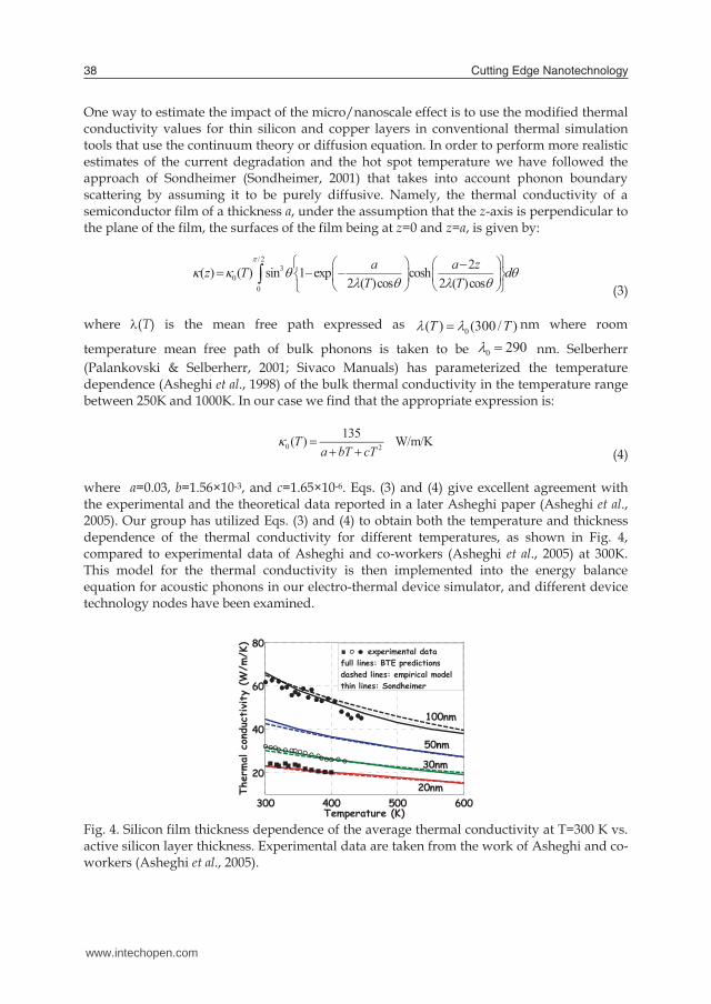
One way to estimate the impact of the micro/nanoscale effect is to use the modified thermal conductivity values for thin silicon and copper layers in conventional thermal simulation tools that use the continuum theory or diffusion equation. In order to perform more realistic estimates of the current degradation and the hot spot temperature we have followed the approach of Sondheimer (Sondheimer, 2001) that takes into account phonon boundary scattering by assuming it to be purely diffusive. Namely, the thermal conductivity of a semiconductor film of a thickness a, under the assumption that the z-axis is perpendicular to the plane of the film, the surfaces of the film being at z=0 and z=a, is given by:
/23
00
2( ) ( ) sin 1 exp cosh2 ( )cos 2 ( )cos
a a zz T dT T
(3) where (T) is the mean free path expressed as
0( ) (300 / )T T nm where room
temperature mean free path of bulk phonons is taken to be 0 290 nm. Selberherr
(Palankovski & Selberherr, 2001; Sivaco Manuals) has parameterized the temperature dependence (Asheghi et al., 1998) of the bulk thermal conductivity in the temperature range between 250K and 1000K. In our case we find that the appropriate expression is:
0 2
135( ) W/m/KTa bT cT
(4) where a=0.03, b=1.56×10⁻³, and c=1.65×10⁻⁶. Eqs. (3) and (4) give excellent agreement with the experimental and the theoretical data reported in a later Asheghi paper (Asheghi et al., 2005). Our group has utilized Eqs. (3) and (4) to obtain both the temperature and thickness dependence of the thermal conductivity for different temperatures, as shown in Fig. 4, compared to experimental data of Asheghi and co-workers (Asheghi et al., 2005) at 300K. This model for the thermal conductivity is then implemented into the energy balance equation for acoustic phonons in our electro-thermal device simulator, and different device technology nodes have been examined.
300 400 500 600
20
40
60
80
Temperature (K)
The
rmal c
ondu
ctivity
(W/m
/K)
experimental datafull lines: BTE predictionsdashed lines: empirical modelthin lines: Sondheimer
20nm
30nm
50nm
100nm
Fig. 4. Silicon film thickness dependence of the average thermal conductivity at T=300 K vs. active silicon layer thickness. Experimental data are taken from the work of Asheghi and co-workers (Asheghi et al., 2005).
In the ultra-fast laser heating processes at time scales of 10-15 to 10-12 seconds, as well as high speed transistors switching at timescales in the order of 10-11 seconds, the temperatures of the electron and phonon systems are not in equilibrium and may differ by orders of magnitude. Even after the phonon and electron reach equilibrium, the energy carried away by phonons can travel only to 10-100 nanometers; therefore, the temperature of the transistor can easily rise to several times its designed reliability limit. Under these circumstances, regardless of the cooling solution at the packaging level, a catastrophic failure at the device level can occur, because the impact of the rapid temperature rise is limited to the device and its vicinity. As a result, while the package level cooling solutions can reduce the quasi steady-state/average temperature across a microprocessor or at length scales in the order of one millimeter, it has very little impact at micro/nanoscales. Basically, there is no practical way to reduce the temperature at the device and interconnect level by means of a cooling device or solution; therefore, the options for thermal engineering of these devices are very limited. However, intelligent electro-thermal design along with careful floor planning at the device level can largely reduce the temperature rise within a device. This means that the role of the thermal engineer is to properly anticipate – perhaps in full collaboration with electrical engineers – and prevent the problem at the early stages and at the device level, rather than to pass the problem to the package-level thermal engineers.
3. Early attempts to Modeling Heating Effects in State of the Art Devices
In order to understand the modeling of heating effects in commercial device simulators, we first derive the differential equation of heat conduction for a stationary, homogeneous, isotropic solid with heat generation within the body. Heat generation in general may be due to nuclear, electrical, chemical, or other sources that may be a function of time and/or position. The heat generation rate in the medium, generally specified as heat generation per unit time, per unit volume, is denoted H(r,t) and is given in W/m3. We consider the energy balance equation for a small control volume stated as: rate of heat entering through the bounding surfaces of V + rate of energy generation in V = rate of storage of energy in V. In other words the rate of heat entering through the bounding surfaces of V (term 1) is:
1
A V
Term q ndA qdV (5)
where A is the surface area of the volume element V, n is the outward-drawn normal unit vector to the surface element dA, q is the heat flux vector at dA; here the minus sign is included to ensure that the heat flow is into the volume element V, and the divergence theorem is used to convert the surface integral to volume integral. The remaining two terms are evaluated as: Term2 = Rate of energy generation in V = ( , )
V
H r t dV (6)
Term3 = rate of energy storage in V = ( , )
VV
T r tC dVt
(7)
www.intechopen.com
Heating Effects in Nanoscale Devices 39
One way to estimate the impact of the micro/nanoscale effect is to use the modified thermal conductivity values for thin silicon and copper layers in conventional thermal simulation tools that use the continuum theory or diffusion equation. In order to perform more realistic estimates of the current degradation and the hot spot temperature we have followed the approach of Sondheimer (Sondheimer, 2001) that takes into account phonon boundary scattering by assuming it to be purely diffusive. Namely, the thermal conductivity of a semiconductor film of a thickness a, under the assumption that the z-axis is perpendicular to the plane of the film, the surfaces of the film being at z=0 and z=a, is given by:
/23
00
2( ) ( ) sin 1 exp cosh2 ( )cos 2 ( )cos
a a zz T dT T
(3) where (T) is the mean free path expressed as
0( ) (300 / )T T nm where room
temperature mean free path of bulk phonons is taken to be 0 290 nm. Selberherr
(Palankovski & Selberherr, 2001; Sivaco Manuals) has parameterized the temperature dependence (Asheghi et al., 1998) of the bulk thermal conductivity in the temperature range between 250K and 1000K. In our case we find that the appropriate expression is:
0 2
135( ) W/m/KTa bT cT
(4) where a=0.03, b=1.56×10⁻³, and c=1.65×10⁻⁶. Eqs. (3) and (4) give excellent agreement with the experimental and the theoretical data reported in a later Asheghi paper (Asheghi et al., 2005). Our group has utilized Eqs. (3) and (4) to obtain both the temperature and thickness dependence of the thermal conductivity for different temperatures, as shown in Fig. 4, compared to experimental data of Asheghi and co-workers (Asheghi et al., 2005) at 300K. This model for the thermal conductivity is then implemented into the energy balance equation for acoustic phonons in our electro-thermal device simulator, and different device technology nodes have been examined.
300 400 500 600
20
40
60
80
Temperature (K)
The
rmal c
ondu
ctivity
(W/m
/K)
experimental datafull lines: BTE predictionsdashed lines: empirical modelthin lines: Sondheimer
20nm
30nm
50nm
100nm
Fig. 4. Silicon film thickness dependence of the average thermal conductivity at T=300 K vs. active silicon layer thickness. Experimental data are taken from the work of Asheghi and co-workers (Asheghi et al., 2005).
In the ultra-fast laser heating processes at time scales of 10-15 to 10-12 seconds, as well as high speed transistors switching at timescales in the order of 10-11 seconds, the temperatures of the electron and phonon systems are not in equilibrium and may differ by orders of magnitude. Even after the phonon and electron reach equilibrium, the energy carried away by phonons can travel only to 10-100 nanometers; therefore, the temperature of the transistor can easily rise to several times its designed reliability limit. Under these circumstances, regardless of the cooling solution at the packaging level, a catastrophic failure at the device level can occur, because the impact of the rapid temperature rise is limited to the device and its vicinity. As a result, while the package level cooling solutions can reduce the quasi steady-state/average temperature across a microprocessor or at length scales in the order of one millimeter, it has very little impact at micro/nanoscales. Basically, there is no practical way to reduce the temperature at the device and interconnect level by means of a cooling device or solution; therefore, the options for thermal engineering of these devices are very limited. However, intelligent electro-thermal design along with careful floor planning at the device level can largely reduce the temperature rise within a device. This means that the role of the thermal engineer is to properly anticipate – perhaps in full collaboration with electrical engineers – and prevent the problem at the early stages and at the device level, rather than to pass the problem to the package-level thermal engineers.
3. Early attempts to Modeling Heating Effects in State of the Art Devices
In order to understand the modeling of heating effects in commercial device simulators, we first derive the differential equation of heat conduction for a stationary, homogeneous, isotropic solid with heat generation within the body. Heat generation in general may be due to nuclear, electrical, chemical, or other sources that may be a function of time and/or position. The heat generation rate in the medium, generally specified as heat generation per unit time, per unit volume, is denoted H(r,t) and is given in W/m3. We consider the energy balance equation for a small control volume stated as: rate of heat entering through the bounding surfaces of V + rate of energy generation in V = rate of storage of energy in V. In other words the rate of heat entering through the bounding surfaces of V (term 1) is:
1
A V
Term q ndA qdV (5)
where A is the surface area of the volume element V, n is the outward-drawn normal unit vector to the surface element dA, q is the heat flux vector at dA; here the minus sign is included to ensure that the heat flow is into the volume element V, and the divergence theorem is used to convert the surface integral to volume integral. The remaining two terms are evaluated as: Term2 = Rate of energy generation in V = ( , )
V
H r t dV (6)
Term3 = rate of energy storage in V = ( , )
VV
T r tC dVt
(7)
www.intechopen.com
Cutting Edge Nanotechnology40
Combining Eqs. (5) – (7) yields: ( , )( , ) ( , ) 0V
V
T r tq r t H r t C dVt
(8)
The last equation is derived for an arbitrary small volume element V within the solid, hence the volume V may be chosen so small as to remove the integral and one obtains: ( , )( , ) ( , ) V
T r tq r t H r t Ct
(9)
Substituting q(r,t) from Eq. (1) into Eq. (9) finally yields the differential equation of heat conduction for a stationary, homogeneous, isotropic solid with heat generation within the body as: ( , ) ( , )( , ) ( , ) V
T r t T r tT r t H r t C ct t
(10)
The energy generation term in Eq. (10) is discussed in more details in Section 3.1 below.
3.1 Form of the Heat Source Term Lai and Majumdar (Lai & Majumdar, 1996) developed a coupled electro-thermal model for studying thermal non-equilibrium in submicron silicon MOSFETs. Their results showed that the highest electron and lattice temperatures occur under the drain side of the gate electrode, which, also corresponds to the region where non-equilibrium effects such as impact ionization and velocity overshoot are maximum. Majumdar et al. (Majumdar et al., 1995) have analyzed the variation of hot electrons and associated hot phonon effects in GaAs MESFETs. These hot carriers were observed to decrease the output drain current by as much as 15%. Thus, they concluded that both electron and lattice heating should be included in the electrical behavior of devices. As it has been recognized that the simulation of devices operated under non-isothermal conditions was of growing importance, the heat flow equation given in Eq. (10) has been added to conventional drift-diffusion and/or hydrodynamic models to account for the mobility degradation due to lattice heating. There has been a discussion on the form of the heat generation term, details of which can be found in an excellent paper by Wachutka (Wachutka, 1990). Briefly, three different models are most commonly used and these include: (1) Joule Heating, (2) electron-lattice scattering and (3) the phonon model. Although these three models yield identical results in equilibrium, under non-equilibrium conditions the results of the three models can vary significantly.
Case 1: Within the Joule heating model, the thermal model consists of the heat diffusion equation using a Joule heating term as the source. The source term is computed from the electrical solution as the product of the local field and the current density (Gaur &,Navon, 1976)
H J E (11)
This source term is similar to the one used by Leung and co-workers (Leung et al., 1997) and assumes that recombination heating is negligible. In this case the “hot spot” will occur near the location where the dot product of the field and of the current density is the largest. Simulations that have used this expression as a heating term suggest that the bulk of the heating will occur directly under the gate region where most of the voltage drop occurs and where the current density is the largest because of the restricted electron flow path due to the depletion regions. A study by Raman and co-workers on lightly doped drain (LDD) devices suggested that the location of the hot-spot occurs at the drain side of the gate. The complete Leung and co-workers expression used for the source term is H J E+( - )( 3 )G BR G E k T (12) where the second term represents the heating rate due to non-radiative generation (G) and recombination (R) of electron-hole pairs. EG is the semiconductor band-gap, kB is the Boltzmann constant and T is the lattice temperature.
Case 2: Within the electron-lattice scattering model, the thermal system is represented as a single lattice temperature and is considered to be in thermal equilibrium. However, since the heat generation is due to non-equilibrium electron temperatures, the source term is then taken as a scattering term obtained from the relaxation time approximation and moments of the BTE. In essence, the transport is similar to case 1 in that the heat diffusion equation governs transport in the solid, except for the fact that the source term is now given as a moment of the relaxation time approximation, i.e.
32
e LB
e L
T TkH
(13)
In the above expression Te is the electron temperature, TL is the lattice temperature and e-L is the electron lattice scattering time constant. Case 3: Phonon-model. Under thermal non-equilibrium conditions a system of two phonons is used as represented later in the text. In this case, the ‘lattice’ temperature is taken to be the acoustic phonon temperature TA, because this is the mode responsible for diffusion. The energy balance equations for the acoustic and optical modes were for the first time derived by Majumdar and co-workers starting from the phonons Boltzmann transport equation. In all our investigations we have pursued this approach for the description of the phonon bath. A variant of this approach, that has been pursued by the Leeds group (Sadi et al., 2007) and by Eric Pop and co-workers [Pop, 2006], counts the number of generated acoustic and optical phonons in a given branch and mode. Then, the total heat generation rate per unit volume is computed as
ems abs
sim
nHN t
(14)
www.intechopen.com
Heating Effects in Nanoscale Devices 41
Combining Eqs. (5) – (7) yields: ( , )( , ) ( , ) 0V
V
T r tq r t H r t C dVt
(8)
The last equation is derived for an arbitrary small volume element V within the solid, hence the volume V may be chosen so small as to remove the integral and one obtains: ( , )( , ) ( , ) V
T r tq r t H r t Ct
(9)
Substituting q(r,t) from Eq. (1) into Eq. (9) finally yields the differential equation of heat conduction for a stationary, homogeneous, isotropic solid with heat generation within the body as: ( , ) ( , )( , ) ( , ) V
T r t T r tT r t H r t C ct t
(10)
The energy generation term in Eq. (10) is discussed in more details in Section 3.1 below.
3.1 Form of the Heat Source Term Lai and Majumdar (Lai & Majumdar, 1996) developed a coupled electro-thermal model for studying thermal non-equilibrium in submicron silicon MOSFETs. Their results showed that the highest electron and lattice temperatures occur under the drain side of the gate electrode, which, also corresponds to the region where non-equilibrium effects such as impact ionization and velocity overshoot are maximum. Majumdar et al. (Majumdar et al., 1995) have analyzed the variation of hot electrons and associated hot phonon effects in GaAs MESFETs. These hot carriers were observed to decrease the output drain current by as much as 15%. Thus, they concluded that both electron and lattice heating should be included in the electrical behavior of devices. As it has been recognized that the simulation of devices operated under non-isothermal conditions was of growing importance, the heat flow equation given in Eq. (10) has been added to conventional drift-diffusion and/or hydrodynamic models to account for the mobility degradation due to lattice heating. There has been a discussion on the form of the heat generation term, details of which can be found in an excellent paper by Wachutka (Wachutka, 1990). Briefly, three different models are most commonly used and these include: (1) Joule Heating, (2) electron-lattice scattering and (3) the phonon model. Although these three models yield identical results in equilibrium, under non-equilibrium conditions the results of the three models can vary significantly.
Case 1: Within the Joule heating model, the thermal model consists of the heat diffusion equation using a Joule heating term as the source. The source term is computed from the electrical solution as the product of the local field and the current density (Gaur &,Navon, 1976)
H J E (11)
This source term is similar to the one used by Leung and co-workers (Leung et al., 1997) and assumes that recombination heating is negligible. In this case the “hot spot” will occur near the location where the dot product of the field and of the current density is the largest. Simulations that have used this expression as a heating term suggest that the bulk of the heating will occur directly under the gate region where most of the voltage drop occurs and where the current density is the largest because of the restricted electron flow path due to the depletion regions. A study by Raman and co-workers on lightly doped drain (LDD) devices suggested that the location of the hot-spot occurs at the drain side of the gate. The complete Leung and co-workers expression used for the source term is H J E+( - )( 3 )G BR G E k T (12) where the second term represents the heating rate due to non-radiative generation (G) and recombination (R) of electron-hole pairs. EG is the semiconductor band-gap, kB is the Boltzmann constant and T is the lattice temperature.
Case 2: Within the electron-lattice scattering model, the thermal system is represented as a single lattice temperature and is considered to be in thermal equilibrium. However, since the heat generation is due to non-equilibrium electron temperatures, the source term is then taken as a scattering term obtained from the relaxation time approximation and moments of the BTE. In essence, the transport is similar to case 1 in that the heat diffusion equation governs transport in the solid, except for the fact that the source term is now given as a moment of the relaxation time approximation, i.e.
32
e LB
e L
T TkH
(13)
In the above expression Te is the electron temperature, TL is the lattice temperature and e-L is the electron lattice scattering time constant. Case 3: Phonon-model. Under thermal non-equilibrium conditions a system of two phonons is used as represented later in the text. In this case, the ‘lattice’ temperature is taken to be the acoustic phonon temperature TA, because this is the mode responsible for diffusion. The energy balance equations for the acoustic and optical modes were for the first time derived by Majumdar and co-workers starting from the phonons Boltzmann transport equation. In all our investigations we have pursued this approach for the description of the phonon bath. A variant of this approach, that has been pursued by the Leeds group (Sadi et al., 2007) and by Eric Pop and co-workers [Pop, 2006], counts the number of generated acoustic and optical phonons in a given branch and mode. Then, the total heat generation rate per unit volume is computed as
ems abs
sim
nHN t
(14)
www.intechopen.com
Cutting Edge Nanotechnology42
where n is the electron density, Nsim is the number of simulated particles and Δt is the simulation time. In our opinion, the best solution to the submicron heat transport problem only has been provided by Narumanchi and co-workers (Naramunchi, 2004). In their recent study they propose a model based on the solution of the BTE, accounting for the transverse acoustic and longitudinal acoustic as well as optical phonons. Their model incorporates realistic phonon dispersion curves for silicon. The interactions among the different phonon branches and different phonon frequencies are considered and the proposed model satisfies energy conservation. Frequency-dependent relaxation times, obtained from perturbation theory, and accounting for phonon interaction rules, are used. In the calculation of the relaxation rates, they have included impurity scattering and the three-phonon interactions (the normall (N) process and the Umklapp (U) process). U processes pose direct thermal resistance while N processes influence the thermal resistance by altering the phonon distribution function. In this study, the BTE is numerically solved using a structured finite volume approach. Using this model, experimental in-plane thermal conductivity data for silicon thin films over a wide range of temperatures are matched satisfactorily.
4. The ASU Approach to Solving Lattice Heating Problem in Nanoscale Devices
To properly treat heating without any approximations made in the problem at hand, one in principle has to solve the coupled Boltzmann transport equations for the electron and phonon systems together. More precisely, one has to solve the coupled electron − optical phonons – acoustic phonons – heat bath problem, where each sub-process involves different time scales and has to be addressed in a somewhat individual manner and included in the global picture via a self-consistent loop. Let us consider the coupled system of semi-classical Boltzmann transport equations for the distribution functions of electrons f(k,r,t) and phonons g(k,r,t):
k+q k k+q k k k+q k k+q,q , q , q ,q
q
k+q k k k+q,q ,q
k
(k) r
( )
e r k e a e a
p r e ap p
ev E f W W W Wt
gv q g W Wt t
(16)
Here k+q k
,qeW is the probability for electron transition from k+q to k due to emission of
phonon q. Similarly k+q k,qaW
refers to processes of absorption. The system is nonlinear, as
the probabilities W depend on the product f•g of the electron and phonon distribution functions. The transfer of energy between electrons and phonons is due to the terms W, with a timescale of the order of 0.1 ps (see Fig. 5 below for more details). This equation set poses a multi-scale problem since the left hand sides involve different time scales: the velocity vp of the phonons is two orders of magnitude lower than the velocity ve of the electrons. Accordingly, the heat transfer by the lattice is much slower process than the charge transfer. Note that, when considering the electron lattice coupling, the energy transfer from electrons to the high-energy optical phonons is very efficient. However, optical phonons possess negligible group velocity and, thus, do not participate significantly in the heat diffusion.
They instead must transfer their energy to acoustic phonons, which diffuse heat. The energy transfer between phonons is relatively slow compared to electron-optical phonon transport and, thus, thermal non-equilibrium may also exist between optical and acoustic phonons. Fig. 5 shows the primary path of thermal energy transport and the associated time constants.
High Electric Field
Optical Phonon Emission
Acoustic Phonon Emission
Heat Conduction in Semiconductor
~ 0.1ps ~ 0.1ps
~ 10ps
~ 10ps
Hot Electron Transport
Fig. 5. The most likely path between energy carrying particles in a semiconductor device is shown together with the corresponding scattering time constants. According to Fig. 5, the primary path of energy transport is represented first by scattering between electrons and optical phonons (TLO) and then optical phonons to the lattice (TA) (Tien et al., 1998). The BTE for the two kinds of phonons is then used to provide the energy balance of the process. As we already mentioned, the direct solution of the phonon Boltzmann equation itself is a very difficult task as it is difficult to mathematically express the anharmonic phonon decay process, and in addition to this one has to solve separate phonon Boltzmann equation for each mode of the acoustic and optical branches. As already noted in Section 2 above, some attempts to solve the problem within the relaxation time approximation have been made by Narumanchi and co-workers (Naramunchi et al., 2004). If we now include the electrons and holes into the picture with their corresponding Boltzmann transport equations, then the solution of the electron-hole-phonon coupled set of equations becomes a formidable task even for today’s high performance computing systems. Therefore, some simplifications of this global problem are needed. Since for device simulation we are mainly focused on accurately calculating the IV-characteristics of a device, the self-heating being a by-product of the current flow through the device can be treated in a more approximate manner, but which is still more accurate than the local heat conduction model. Majumder and co-workers (Lai & Majumdar, 1996; Majumdar et al., 1995), starting from the phonon Boltzmann equations derived energy balance equations separately for the optical phonon and the acoustic phonon bath. One can also derive these energy balance equations starting from the energy conservation principle. For electric field, E ≥ 106 V/m, electrons lose energy to optical phonons and optical phonons decay to acoustic phonons. Using the first law of thermodynamics, the energy conservation equations for optical and acoustic phonons are:
coll
LO
coll
eLO
tW
tW
tW
, (17)
www.intechopen.com

Heating Effects in Nanoscale Devices 43
where n is the electron density, Nsim is the number of simulated particles and Δt is the simulation time. In our opinion, the best solution to the submicron heat transport problem only has been provided by Narumanchi and co-workers (Naramunchi, 2004). In their recent study they propose a model based on the solution of the BTE, accounting for the transverse acoustic and longitudinal acoustic as well as optical phonons. Their model incorporates realistic phonon dispersion curves for silicon. The interactions among the different phonon branches and different phonon frequencies are considered and the proposed model satisfies energy conservation. Frequency-dependent relaxation times, obtained from perturbation theory, and accounting for phonon interaction rules, are used. In the calculation of the relaxation rates, they have included impurity scattering and the three-phonon interactions (the normall (N) process and the Umklapp (U) process). U processes pose direct thermal resistance while N processes influence the thermal resistance by altering the phonon distribution function. In this study, the BTE is numerically solved using a structured finite volume approach. Using this model, experimental in-plane thermal conductivity data for silicon thin films over a wide range of temperatures are matched satisfactorily.
4. The ASU Approach to Solving Lattice Heating Problem in Nanoscale Devices
To properly treat heating without any approximations made in the problem at hand, one in principle has to solve the coupled Boltzmann transport equations for the electron and phonon systems together. More precisely, one has to solve the coupled electron − optical phonons – acoustic phonons – heat bath problem, where each sub-process involves different time scales and has to be addressed in a somewhat individual manner and included in the global picture via a self-consistent loop. Let us consider the coupled system of semi-classical Boltzmann transport equations for the distribution functions of electrons f(k,r,t) and phonons g(k,r,t):
k+q k k+q k k k+q k k+q,q , q , q ,q
q
k+q k k k+q,q ,q
k
(k) r
( )
e r k e a e a
p r e ap p
ev E f W W W Wt
gv q g W Wt t
(16)
Here k+q k
,qeW is the probability for electron transition from k+q to k due to emission of
phonon q. Similarly k+q k,qaW
refers to processes of absorption. The system is nonlinear, as
the probabilities W depend on the product f•g of the electron and phonon distribution functions. The transfer of energy between electrons and phonons is due to the terms W, with a timescale of the order of 0.1 ps (see Fig. 5 below for more details). This equation set poses a multi-scale problem since the left hand sides involve different time scales: the velocity vp of the phonons is two orders of magnitude lower than the velocity ve of the electrons. Accordingly, the heat transfer by the lattice is much slower process than the charge transfer. Note that, when considering the electron lattice coupling, the energy transfer from electrons to the high-energy optical phonons is very efficient. However, optical phonons possess negligible group velocity and, thus, do not participate significantly in the heat diffusion.
They instead must transfer their energy to acoustic phonons, which diffuse heat. The energy transfer between phonons is relatively slow compared to electron-optical phonon transport and, thus, thermal non-equilibrium may also exist between optical and acoustic phonons. Fig. 5 shows the primary path of thermal energy transport and the associated time constants.
High Electric Field
Optical Phonon Emission
Acoustic Phonon Emission
Heat Conduction in Semiconductor
~ 0.1ps ~ 0.1ps
~ 10ps
~ 10ps
Hot Electron Transport
Fig. 5. The most likely path between energy carrying particles in a semiconductor device is shown together with the corresponding scattering time constants. According to Fig. 5, the primary path of energy transport is represented first by scattering between electrons and optical phonons (TLO) and then optical phonons to the lattice (TA) (Tien et al., 1998). The BTE for the two kinds of phonons is then used to provide the energy balance of the process. As we already mentioned, the direct solution of the phonon Boltzmann equation itself is a very difficult task as it is difficult to mathematically express the anharmonic phonon decay process, and in addition to this one has to solve separate phonon Boltzmann equation for each mode of the acoustic and optical branches. As already noted in Section 2 above, some attempts to solve the problem within the relaxation time approximation have been made by Narumanchi and co-workers (Naramunchi et al., 2004). If we now include the electrons and holes into the picture with their corresponding Boltzmann transport equations, then the solution of the electron-hole-phonon coupled set of equations becomes a formidable task even for today’s high performance computing systems. Therefore, some simplifications of this global problem are needed. Since for device simulation we are mainly focused on accurately calculating the IV-characteristics of a device, the self-heating being a by-product of the current flow through the device can be treated in a more approximate manner, but which is still more accurate than the local heat conduction model. Majumder and co-workers (Lai & Majumdar, 1996; Majumdar et al., 1995), starting from the phonon Boltzmann equations derived energy balance equations separately for the optical phonon and the acoustic phonon bath. One can also derive these energy balance equations starting from the energy conservation principle. For electric field, E ≥ 106 V/m, electrons lose energy to optical phonons and optical phonons decay to acoustic phonons. Using the first law of thermodynamics, the energy conservation equations for optical and acoustic phonons are:
coll
LO
coll
eLO
tW
tW
tW
, (17)
www.intechopen.com
Cutting Edge Nanotechnology44
coll
LOAA
A
tWT
tW
)( , (18)
We, WLO and WA are electron, optical phonon and acoustic phonon energy densities, respectively. We next use
LOLOLO dTCdW and AAA dTCdW (19) where CLO (specific heat capacity for optical phonons) can be estimated from Einstein model, while CA (specific heat capacity for acoustic phonons) from Debye model. Next, the collision terms are expressed using the relaxation time approximation (RTA):
phe
phBdeB
coll
eTkvmTk
ntW
23
21
23 2*
, (20)
ALO
ALOLO
coll
LO TTCtW
, (21)
where Te is the electron temperature, vd is the electron drift velocity and Tph can be optical or acoustic phonon temperature depending on which kind of phonons electrons interact with. Combining Eqs. (17)-(21), one gets:
ALO
ALOLO
LOe
d
LOe
LOeB
LOLO
TTCvnmTTnktTC 22
3 2*
(22a)
ALO
ALOLOAA
AA
TTCTtTC )( . (22b)
For electric field, E<106 V/m, electrons lose energy directly to acoustic phonons and in that case:
coll
eAA
AA t
WTtTC
)( (23a)
Ae
deB
AAe
BAA
AA
vmTknTnkT
tTC
2*
21
23
23)( (23b)
Under the assumption of very low electric fields, the electron temperature and acoustic phonon temperature equal the lattice temperature and terms 2 and 3 in Eq. (23) cancel. Using the low field conductivity and the mobility expressions we get that the heat source term reduces to the last term of Eq. (23b). Namely
2 2
22
*d dgen
v nm vq J E E (24)
where it is assumed that for low doping concentrations the relaxation time that appears in Eq. (24) is the acoustic phonon relaxation time since acoustic phonon scattering, being isotropic scattering process, is most effective in randomizing the carrier momentum when the carrier energy is very low (low applied electric fields). In our electro-thermal simulator, we solve steady-state versions of the Eqs. (22a) and (22b) for the optical and acoustic phonon temperatures self consistently with the Monte Carlo simulation of the electron Boltzmann transport equation for modeling n-channel fully-depleted (FD) silicon on insulator (SOI) devices. In other words, to simplify the calculations to a tractable form in the present work, we have used a Chapman-Enskog type expansion (Cercignani, 1988) to replace the microscopic phonon transport equation by a diffusion problem for the local density and energy of the phonons, where the diffusion coefficients are dependent on the state of the electrons. This method involves computation of the phonon energy dependent scattering tables in the Ensemble Monte Carlo (EMC) code for the electron transport, which already represents a big improvement over the current state of the art, where, as already discussed, the coupling of thermal and charge effects is strictly one way. This approach also takes care of the multi-scale nature of the problem, assuming a quasi steady state: the phonons are in steady state, albeit with a spatially dependent temperature distribution. In the present work we neglect the effect of the optical phonon dispersion on the tabulated scattering rates. Using our electro-thermal simulator we demonstrate that, contrary to earlier predictions, the non-locality of the electron transport and velocity overshoot effects significantly reduce current degradation in nanoscale devices due to the fact that carriers traveling ballistically do not dissipate energy in the active region of the device, rather in the drain contact. We also show that in nanoscale devices, the hotspot corresponding to the peak temperature moves towards the drain end of the channel where removal of heat is more effective, and where less effect on the transport dynamics occurs underneath the gate.
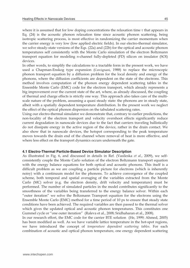
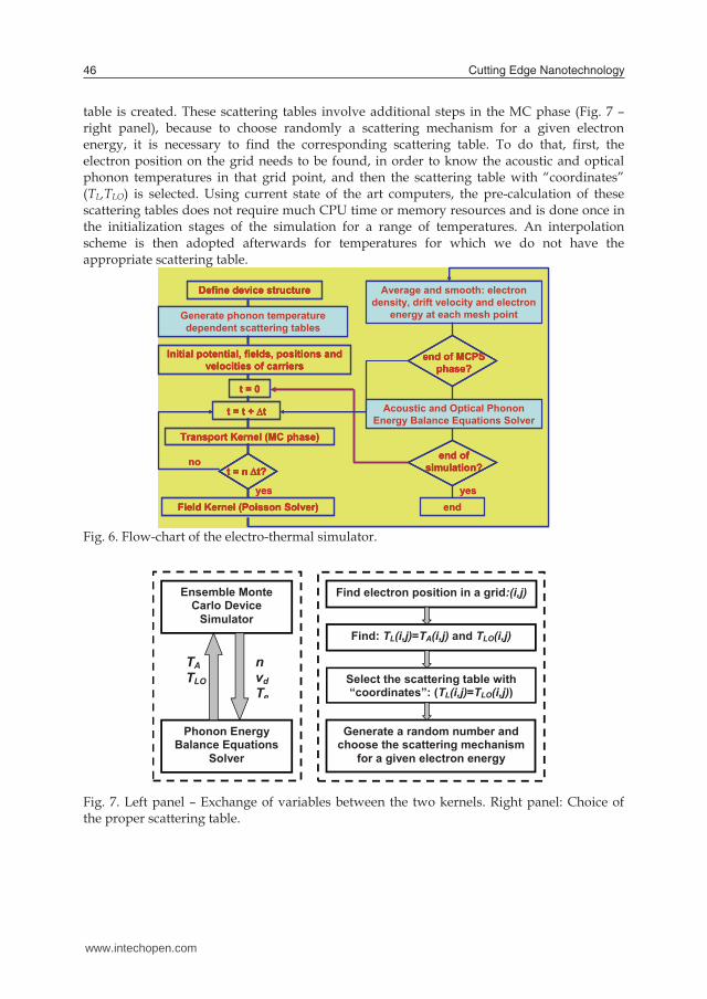
4.1 Electro-Thermal Particle-Based Device Simulator Description As illustrated in Fig. 6, and discussed in details in Ref. (Vasileska et al., 2009), we self-consistently couple the Monte Carlo solution of the electron Boltzmann transport equation with the energy balance equations for both optical and acoustic phonons. This itself is a difficult problem as we are coupling a particle picture for electrons (which is inherently noisy) with a continuum model for the phonons. To achieve convergence of the coupled scheme, both temporal and spatial averaging of the variables extracted from the Monte Carlo (MC) solver (e.g. the electron density, drift velocity and temperature) must be performed. The number of simulated particles in the model contributes significantly to the smoothness of the variables being transferred to the energy balance solver. Within each “outer iteration” we solve the Boltzmann Transport equation for the electrons using the Ensemble Monte Carlo (EMC) method for a time period of 10 ps to ensure that steady state conditions have been achieved. The required variables are then passed to the thermal solver which gives the updated optical and acoustic phonon temperatures. This constitutes one Gummel cycle or “one outer iteration” (Raleva et al., 2008; Sridhaharan et al., 2008). In our research effort, the EMC code for the carrier BTE solution (He, 1999; Ahmed, 2005) has been modified as well. As we have variable lattice temperature in the hot-spot regions, we have introduced the concept of temperature dependent scattering tables. For each combination of acoustic and optical phonon temperature, one energy dependent scattering
www.intechopen.com
Heating Effects in Nanoscale Devices 45
coll
LOAA
A
tWT
tW
)( , (18)
We, WLO and WA are electron, optical phonon and acoustic phonon energy densities, respectively. We next use
LOLOLO dTCdW and AAA dTCdW (19) where CLO (specific heat capacity for optical phonons) can be estimated from Einstein model, while CA (specific heat capacity for acoustic phonons) from Debye model. Next, the collision terms are expressed using the relaxation time approximation (RTA):
phe
phBdeB
coll
eTkvmTk
ntW
23
21
23 2*
, (20)
ALO
ALOLO
coll
LO TTCtW
, (21)
where Te is the electron temperature, vd is the electron drift velocity and Tph can be optical or acoustic phonon temperature depending on which kind of phonons electrons interact with. Combining Eqs. (17)-(21), one gets:
ALO
ALOLO
LOe
d
LOe
LOeB
LOLO
TTCvnmTTnktTC 22
3 2*
(22a)
ALO
ALOLOAA
AA
TTCTtTC )( . (22b)
For electric field, E<106 V/m, electrons lose energy directly to acoustic phonons and in that case:
coll
eAA
AA t
WTtTC
)( (23a)
Ae
deB
AAe
BAA
AA
vmTknTnkT
tTC
2*
21
23
23)( (23b)
Under the assumption of very low electric fields, the electron temperature and acoustic phonon temperature equal the lattice temperature and terms 2 and 3 in Eq. (23) cancel. Using the low field conductivity and the mobility expressions we get that the heat source term reduces to the last term of Eq. (23b). Namely
2 2
22
*d dgen
v nm vq J E E (24)
where it is assumed that for low doping concentrations the relaxation time that appears in Eq. (24) is the acoustic phonon relaxation time since acoustic phonon scattering, being isotropic scattering process, is most effective in randomizing the carrier momentum when the carrier energy is very low (low applied electric fields). In our electro-thermal simulator, we solve steady-state versions of the Eqs. (22a) and (22b) for the optical and acoustic phonon temperatures self consistently with the Monte Carlo simulation of the electron Boltzmann transport equation for modeling n-channel fully-depleted (FD) silicon on insulator (SOI) devices. In other words, to simplify the calculations to a tractable form in the present work, we have used a Chapman-Enskog type expansion (Cercignani, 1988) to replace the microscopic phonon transport equation by a diffusion problem for the local density and energy of the phonons, where the diffusion coefficients are dependent on the state of the electrons. This method involves computation of the phonon energy dependent scattering tables in the Ensemble Monte Carlo (EMC) code for the electron transport, which already represents a big improvement over the current state of the art, where, as already discussed, the coupling of thermal and charge effects is strictly one way. This approach also takes care of the multi-scale nature of the problem, assuming a quasi steady state: the phonons are in steady state, albeit with a spatially dependent temperature distribution. In the present work we neglect the effect of the optical phonon dispersion on the tabulated scattering rates. Using our electro-thermal simulator we demonstrate that, contrary to earlier predictions, the non-locality of the electron transport and velocity overshoot effects significantly reduce current degradation in nanoscale devices due to the fact that carriers traveling ballistically do not dissipate energy in the active region of the device, rather in the drain contact. We also show that in nanoscale devices, the hotspot corresponding to the peak temperature moves towards the drain end of the channel where removal of heat is more effective, and where less effect on the transport dynamics occurs underneath the gate.
4.1 Electro-Thermal Particle-Based Device Simulator Description As illustrated in Fig. 6, and discussed in details in Ref. (Vasileska et al., 2009), we self-consistently couple the Monte Carlo solution of the electron Boltzmann transport equation with the energy balance equations for both optical and acoustic phonons. This itself is a difficult problem as we are coupling a particle picture for electrons (which is inherently noisy) with a continuum model for the phonons. To achieve convergence of the coupled scheme, both temporal and spatial averaging of the variables extracted from the Monte Carlo (MC) solver (e.g. the electron density, drift velocity and temperature) must be performed. The number of simulated particles in the model contributes significantly to the smoothness of the variables being transferred to the energy balance solver. Within each “outer iteration” we solve the Boltzmann Transport equation for the electrons using the Ensemble Monte Carlo (EMC) method for a time period of 10 ps to ensure that steady state conditions have been achieved. The required variables are then passed to the thermal solver which gives the updated optical and acoustic phonon temperatures. This constitutes one Gummel cycle or “one outer iteration” (Raleva et al., 2008; Sridhaharan et al., 2008). In our research effort, the EMC code for the carrier BTE solution (He, 1999; Ahmed, 2005) has been modified as well. As we have variable lattice temperature in the hot-spot regions, we have introduced the concept of temperature dependent scattering tables. For each combination of acoustic and optical phonon temperature, one energy dependent scattering
www.intechopen.com
Cutting Edge Nanotechnology46
table is created. These scattering tables involve additional steps in the MC phase (Fig. 7 – right panel), because to choose randomly a scattering mechanism for a given electron energy, it is necessary to find the corresponding scattering table. To do that, first, the electron position on the grid needs to be found, in order to know the acoustic and optical phonon temperatures in that grid point, and then the scattering table with “coordinates” (TL,TLO) is selected. Using current state of the art computers, the pre-calculation of these scattering tables does not require much CPU time or memory resources and is done once in the initialization stages of the simulation for a range of temperatures. An interpolation scheme is then adopted afterwards for temperatures for which we do not have the appropriate scattering table.
Fig. 6. Flow-chart of the electro-thermal simulator.
Ensemble Monte Carlo Device
Simulator
Phonon Energy Balance Equations
Solver
TA TLO
n vd Te
Find electron position in a grid:(i,j)
Find: TL(i,j)=TA(i,j) and TLO(i,j)
Select the scattering table with “coordinates”: (TL(i,j)=TLO(i,j))
Generate a random number and choose the scattering mechanism
for a given electron energy
Fig. 7. Left panel – Exchange of variables between the two kernels. Right panel: Choice of the proper scattering table.
Average and smooth: electron density, drift velocity and electron
energy at each mesh point
end of MCPS phase?
Acoustic and Optical Phonon Energy Balance Equations Solver
end of simulation?
end
no
yes
Define device structure
Generate phonon temperature dependent scattering tables
Initial potential, fields, positions and velocities of carriers
t = 0
t = t + t
Transport Kernel (MC phase)
Field Kernel (Poisson Solver)
t = n t?
yes
Average and smooth: electron density, drift velocity and electron
energy at each mesh point
end of MCPS phase?
end of MCPS phase?
Acoustic and Optical Phonon Energy Balance Equations Solver
end of simulation?
end of simulation?
end
no
yes
Define device structure
Generate phonon temperature dependent scattering tables
Initial potential, fields, positions and velocities of carriers
t = 0
t = t + t
Transport Kernel (MC phase)
Field Kernel (Poisson Solver)
t = n t?
Define device structure
Generate phonon temperature dependent scattering tables
Initial potential, fields, positions and velocities of carriers
t = 0
t = t + t
Transport Kernel (MC phase)
Field Kernel (Poisson Solver)
t = n t?t = n t?
yes
To properly connect the particle-based picture of electron transport with continuous, “fluid-like” phonon energy balance equations, a space-time averaging and smoothing of electron density, drift velocity and electron energy are included. At the end of each MC time step, the electrons are assigned to the nearest grid point. Then, the drift velocities and thermal energies are averaged with the number of electrons at the corresponding grid points. After the MC phase, a time averaging of electron density, drift velocity and thermal energy is done and the electron temperature distribution is calculated. It is assumed that the drift energy is much smaller than the thermal energy. The smoothing of these variables is necessary, because most of the grid points, especially at the interfaces, are rarely populated with electrons. This leads to very low lattice temperatures in those points. The exchange of variables between electron and phonon solvers is shown on the left panel of Fig. 7. Because SOI devices consist of two distinct regions, the silicon device layer and the buried oxide layer (in which the phonons have significantly smaller mean-free paths), the phonon BTE is solved in the silicon layer to accurately model heat transport, but the simpler heat diffusion equation is used in the amorphous BOX because the characteristic length-scale of conduction is much smaller than the film thickness. The two distinct computational regions are coupled through interface conditions that accounts for differences in material properties. For the coupling of the silicon and oxide solution domains, it is necessary to calculate the flux of energy through the interface between the two materials at each point along the interface for every time step. To simulate the steady-state state behavior of a device, the system is started in some initial condition, with the desired potential applied to the contacts, and then the simulation proceeds in a time stepping manner until steady-state is reached. A common starting point for the initial guess is to start out with charge neutrality, i.e., to assign particles randomly according to the doping profile in the device, so that initially the system is charge neutral on the average. After assigning charges randomly in the device structure, charge is then assigned to each mesh point using an adequate particle mesh (PM) coupling method, and Poisson’s equation is solved. The forces are then interpolated on the grid, and particles are accelerated over the next time step. When the system is driven into a steady-state regime and MC simulation time has elapsed, we calculate the steady-state current through a specified terminal. To continue with the thermal part of the simulation, the average electron density, drift velocity and electron temperature must be calculated on a grid. For the given bias conditions, the average electron density in the channel (Fig. 8) is very high at the Si-SiO2 interface near the source injection barrier, while pinch off region exists near the drain.
www.intechopen.com
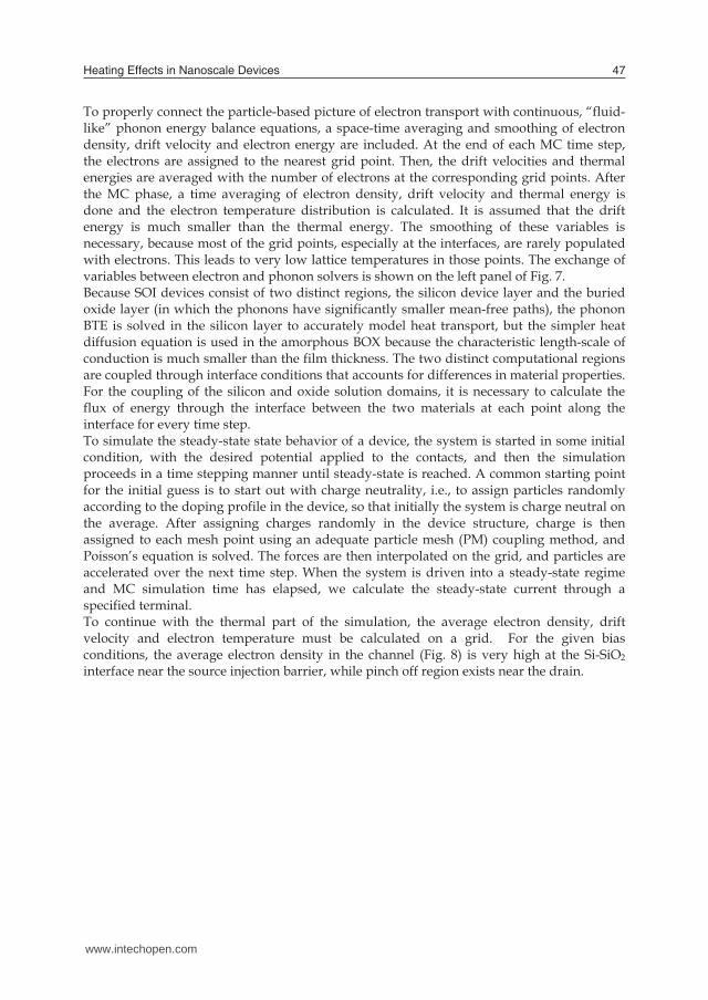
Heating Effects in Nanoscale Devices 47
table is created. These scattering tables involve additional steps in the MC phase (Fig. 7 – right panel), because to choose randomly a scattering mechanism for a given electron energy, it is necessary to find the corresponding scattering table. To do that, first, the electron position on the grid needs to be found, in order to know the acoustic and optical phonon temperatures in that grid point, and then the scattering table with “coordinates” (TL,TLO) is selected. Using current state of the art computers, the pre-calculation of these scattering tables does not require much CPU time or memory resources and is done once in the initialization stages of the simulation for a range of temperatures. An interpolation scheme is then adopted afterwards for temperatures for which we do not have the appropriate scattering table.
Fig. 6. Flow-chart of the electro-thermal simulator.
Ensemble Monte Carlo Device
Simulator
Phonon Energy Balance Equations
Solver
TA TLO
n vd Te
Find electron position in a grid:(i,j)
Find: TL(i,j)=TA(i,j) and TLO(i,j)
Select the scattering table with “coordinates”: (TL(i,j)=TLO(i,j))
Generate a random number and choose the scattering mechanism
for a given electron energy
Fig. 7. Left panel – Exchange of variables between the two kernels. Right panel: Choice of the proper scattering table.
Average and smooth: electron density, drift velocity and electron
energy at each mesh point
end of MCPS phase?
Acoustic and Optical Phonon Energy Balance Equations Solver
end of simulation?
end
no
yes
Define device structure
Generate phonon temperature dependent scattering tables
Initial potential, fields, positions and velocities of carriers
t = 0
t = t + t
Transport Kernel (MC phase)
Field Kernel (Poisson Solver)
t = n t?
yes
Average and smooth: electron density, drift velocity and electron
energy at each mesh point
end of MCPS phase?
end of MCPS phase?
Acoustic and Optical Phonon Energy Balance Equations Solver
end of simulation?
end of simulation?
end
no
yes
Define device structure
Generate phonon temperature dependent scattering tables
Initial potential, fields, positions and velocities of carriers
t = 0
t = t + t
Transport Kernel (MC phase)
Field Kernel (Poisson Solver)
t = n t?
Define device structure
Generate phonon temperature dependent scattering tables
Initial potential, fields, positions and velocities of carriers
t = 0
t = t + t
Transport Kernel (MC phase)
Field Kernel (Poisson Solver)
t = n t?t = n t?
yes
To properly connect the particle-based picture of electron transport with continuous, “fluid-like” phonon energy balance equations, a space-time averaging and smoothing of electron density, drift velocity and electron energy are included. At the end of each MC time step, the electrons are assigned to the nearest grid point. Then, the drift velocities and thermal energies are averaged with the number of electrons at the corresponding grid points. After the MC phase, a time averaging of electron density, drift velocity and thermal energy is done and the electron temperature distribution is calculated. It is assumed that the drift energy is much smaller than the thermal energy. The smoothing of these variables is necessary, because most of the grid points, especially at the interfaces, are rarely populated with electrons. This leads to very low lattice temperatures in those points. The exchange of variables between electron and phonon solvers is shown on the left panel of Fig. 7. Because SOI devices consist of two distinct regions, the silicon device layer and the buried oxide layer (in which the phonons have significantly smaller mean-free paths), the phonon BTE is solved in the silicon layer to accurately model heat transport, but the simpler heat diffusion equation is used in the amorphous BOX because the characteristic length-scale of conduction is much smaller than the film thickness. The two distinct computational regions are coupled through interface conditions that accounts for differences in material properties. For the coupling of the silicon and oxide solution domains, it is necessary to calculate the flux of energy through the interface between the two materials at each point along the interface for every time step. To simulate the steady-state state behavior of a device, the system is started in some initial condition, with the desired potential applied to the contacts, and then the simulation proceeds in a time stepping manner until steady-state is reached. A common starting point for the initial guess is to start out with charge neutrality, i.e., to assign particles randomly according to the doping profile in the device, so that initially the system is charge neutral on the average. After assigning charges randomly in the device structure, charge is then assigned to each mesh point using an adequate particle mesh (PM) coupling method, and Poisson’s equation is solved. The forces are then interpolated on the grid, and particles are accelerated over the next time step. When the system is driven into a steady-state regime and MC simulation time has elapsed, we calculate the steady-state current through a specified terminal. To continue with the thermal part of the simulation, the average electron density, drift velocity and electron temperature must be calculated on a grid. For the given bias conditions, the average electron density in the channel (Fig. 8) is very high at the Si-SiO2 interface near the source injection barrier, while pinch off region exists near the drain.
www.intechopen.com
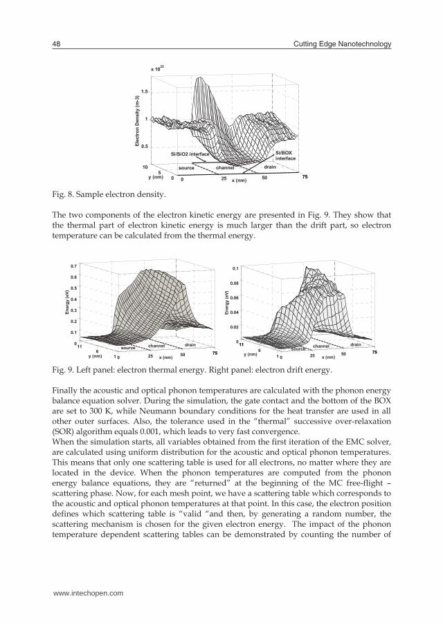
Cutting Edge Nanotechnology48
0 25 50 757505
10
0.5
1
1.5
x 1025
Elec
tron
Den
sity
(m-3
)
Si/SiO2 interface
source drainchannel
Si/BOXinterface
x (nm)y (nm)
Fig. 8. Sample electron density. The two components of the electron kinetic energy are presented in Fig. 9. They show that the thermal part of electron kinetic energy is much larger than the drift part, so electron temperature can be calculated from the thermal energy.
0 25 50 75751
6110
0.1
0.2
0.3
0.4
0.5
0.6
0.7
Ener
gy (e
V)
channelsource drain
x (nm)y (nm) 0 25 50 75751
611110
0.02
0.04
0.06
0.08
0.1
Ener
gy (e
V)
x (nm)y (nm)
channel drainsource
Fig. 9. Left panel: electron thermal energy. Right panel: electron drift energy. Finally the acoustic and optical phonon temperatures are calculated with the phonon energy balance equation solver. During the simulation, the gate contact and the bottom of the BOX are set to 300 K, while Neumann boundary conditions for the heat transfer are used in all other outer surfaces. Also, the tolerance used in the “thermal” successive over-relaxation (SOR) algorithm equals 0.001, which leads to very fast convergence. When the simulation starts, all variables obtained from the first iteration of the EMC solver, are calculated using uniform distribution for the acoustic and optical phonon temperatures. This means that only one scattering table is used for all electrons, no matter where they are located in the device. When the phonon temperatures are computed from the phonon energy balance equations, they are “returned” at the beginning of the MC free-flight – scattering phase. Now, for each mesh point, we have a scattering table which corresponds to the acoustic and optical phonon temperatures at that point. In this case, the electron position defines which scattering table is “valid “and then, by generating a random number, the scattering mechanism is chosen for the given electron energy. The impact of the phonon temperature dependent scattering tables can be demonstrated by counting the number of
energy-exchange electron-phonon scattering events. From the results obtained it could be concluded that the inclusion of the phonon temperature dependent scattering table increases the number of electron-phonon interactions. We have also found that electrons with energies below 50 meV scatter mainly with acoustic phonons in silicon, while those with higher energy scatter strongly with the optical modes. The optical phonon modes have low group velocity (on the order of 1000 m/s) and their occupation is also relatively low, hence they contribute very little to the heat transport. The primary heat carriers in silicon are the faster acoustic phonon modes, which are significantly populated and have group velocities from 5000 m/s for transverse modes to 9000 m/s for longitudinal acoustic modes. Optical phonons decay into acoustic modes, but over relatively long time scales, i.e. picoseconds, compared to the order of tenths of picoseconds (Ferry, 2000). Under high field conditions, this can lead to the creation of a phonon energy bottleneck which can cause the density of optical phonon modes to build up over time, leading to more scattering events and impeding electron transport (Artaki & Price, 1989). To test the overall convergence of the coupled EMC and thermal codes, we registered the variations of the drain current with the number of thermal iterations for a given bias condition. We have simulated 25nm fully-depleted SOI structure (Fig. 10 left panel). The device geometrical dimensions are: channel length = 25 nm, source/drain length=25 nm, Si layer thickness = 10 nm and BOX thickness = 50 nm. The results of simulations given in the right panel of Fig. 10, and show that only 3-5 iterations are necessary to obtain the steady-state solutions of the current.
Source - N+ P Drain - N+
Si02
Gate
Back gate (substrate)
VG1VS
VG2
VD
tox1
tSi
tox2Buried Si02
Source - N+ P Drain - N+
Si02
Gate
Back gate (substrate)
VG1VS
VG2
VD
tox1
tSi
tox2Buried Si02
n-channel 0 20 40 60 80 100
0
2
4
6
8
Number of iterations
Curr
ent
decr
ease
(%)
25nm FD-SOI nMOSFET (Vgs=Vds=1.2V)substrate region is not modeled (Tgate=Tbox=300K)
device width=1um; #electrons=7692device width=3um; #electrons=23842
Fig. 10. Left panel - Cross-section of the simulated devices. Right panel - Current decrease variations with the number of thermal iterations for different number of simulated electrons for 25nm fully-depleted SOI device. For the thermal part of simulations, the bottom of the BOX and the gate electrode are assumed to be isothermal boundaries, set to 300K. Substrate region is not modeled. To further investigate the accuracy of the results and the convergence of the outer current iterative scheme, we increase the device width in order to increase the number of simulated electrons. Namely, the statistical error of the MC method shrinks as the number of simulated carriers, Nsim, increases, and it drops as 1/(Nsim)1/2 (Ferry, 2000). The statistical
www.intechopen.com
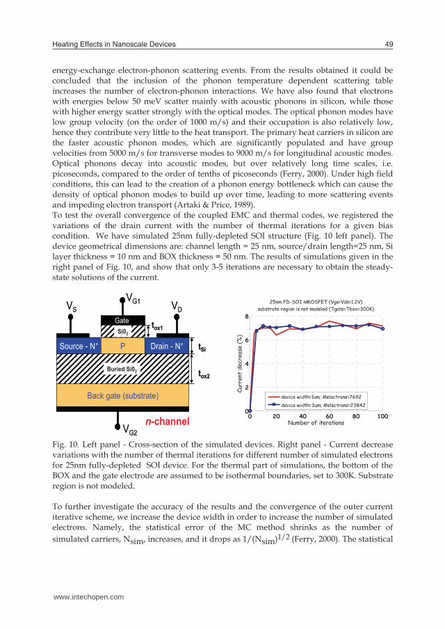
Heating Effects in Nanoscale Devices 49
0 25 50 757505
10
0.5
1
1.5
x 1025
Elec
tron
Den
sity
(m-3
)
Si/SiO2 interface
source drainchannel
Si/BOXinterface
x (nm)y (nm)
Fig. 8. Sample electron density. The two components of the electron kinetic energy are presented in Fig. 9. They show that the thermal part of electron kinetic energy is much larger than the drift part, so electron temperature can be calculated from the thermal energy.
0 25 50 75751
6110
0.1
0.2
0.3
0.4
0.5
0.6
0.7
Ener
gy (e
V)
channelsource drain
x (nm)y (nm) 0 25 50 75751
611110
0.02
0.04
0.06
0.08
0.1
Ener
gy (e
V)
x (nm)y (nm)
channel drainsource
Fig. 9. Left panel: electron thermal energy. Right panel: electron drift energy. Finally the acoustic and optical phonon temperatures are calculated with the phonon energy balance equation solver. During the simulation, the gate contact and the bottom of the BOX are set to 300 K, while Neumann boundary conditions for the heat transfer are used in all other outer surfaces. Also, the tolerance used in the “thermal” successive over-relaxation (SOR) algorithm equals 0.001, which leads to very fast convergence. When the simulation starts, all variables obtained from the first iteration of the EMC solver, are calculated using uniform distribution for the acoustic and optical phonon temperatures. This means that only one scattering table is used for all electrons, no matter where they are located in the device. When the phonon temperatures are computed from the phonon energy balance equations, they are “returned” at the beginning of the MC free-flight – scattering phase. Now, for each mesh point, we have a scattering table which corresponds to the acoustic and optical phonon temperatures at that point. In this case, the electron position defines which scattering table is “valid “and then, by generating a random number, the scattering mechanism is chosen for the given electron energy. The impact of the phonon temperature dependent scattering tables can be demonstrated by counting the number of
energy-exchange electron-phonon scattering events. From the results obtained it could be concluded that the inclusion of the phonon temperature dependent scattering table increases the number of electron-phonon interactions. We have also found that electrons with energies below 50 meV scatter mainly with acoustic phonons in silicon, while those with higher energy scatter strongly with the optical modes. The optical phonon modes have low group velocity (on the order of 1000 m/s) and their occupation is also relatively low, hence they contribute very little to the heat transport. The primary heat carriers in silicon are the faster acoustic phonon modes, which are significantly populated and have group velocities from 5000 m/s for transverse modes to 9000 m/s for longitudinal acoustic modes. Optical phonons decay into acoustic modes, but over relatively long time scales, i.e. picoseconds, compared to the order of tenths of picoseconds (Ferry, 2000). Under high field conditions, this can lead to the creation of a phonon energy bottleneck which can cause the density of optical phonon modes to build up over time, leading to more scattering events and impeding electron transport (Artaki & Price, 1989). To test the overall convergence of the coupled EMC and thermal codes, we registered the variations of the drain current with the number of thermal iterations for a given bias condition. We have simulated 25nm fully-depleted SOI structure (Fig. 10 left panel). The device geometrical dimensions are: channel length = 25 nm, source/drain length=25 nm, Si layer thickness = 10 nm and BOX thickness = 50 nm. The results of simulations given in the right panel of Fig. 10, and show that only 3-5 iterations are necessary to obtain the steady-state solutions of the current.
Source - N+ P Drain - N+
Si02
Gate
Back gate (substrate)
VG1VS
VG2
VD
tox1
tSi
tox2Buried Si02
Source - N+ P Drain - N+
Si02
Gate
Back gate (substrate)
VG1VS
VG2
VD
tox1
tSi
tox2Buried Si02
n-channel 0 20 40 60 80 100
0
2
4
6
8
Number of iterations
Curr
ent
decr
ease
(%)
25nm FD-SOI nMOSFET (Vgs=Vds=1.2V)substrate region is not modeled (Tgate=Tbox=300K)
device width=1um; #electrons=7692device width=3um; #electrons=23842
Fig. 10. Left panel - Cross-section of the simulated devices. Right panel - Current decrease variations with the number of thermal iterations for different number of simulated electrons for 25nm fully-depleted SOI device. For the thermal part of simulations, the bottom of the BOX and the gate electrode are assumed to be isothermal boundaries, set to 300K. Substrate region is not modeled. To further investigate the accuracy of the results and the convergence of the outer current iterative scheme, we increase the device width in order to increase the number of simulated electrons. Namely, the statistical error of the MC method shrinks as the number of simulated carriers, Nsim, increases, and it drops as 1/(Nsim)1/2 (Ferry, 2000). The statistical
www.intechopen.com
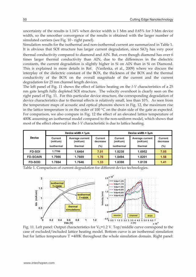
Cutting Edge Nanotechnology50
uncertainty of the results is 1.14% when device width is 1 Mm and 0.65% for 3 Mm device width, so the smoother convergence of the results is obtained with the larger number of simulated carriers (see Fig. 10 - right panel). Simulation results for the isothermal and non-isothermal current are summarized in Table 1. It is obvious that SOI structure has larger current degradation, since SiO2 has very poor thermal conductivity compared to diamond and AlN. But, even though diamond has over 6 times larger thermal conductivity than AlN, due to the differences in the dielectric constants, the current degradation is slightly higher in Si on AlN than in Si on Diamond. This is explained in more details in Ref. (Vasileska, et al., 2009) where we discuss the interplay of the dielectric constant of the BOX, the thickness of the BOX and the thermal conductivity of the BOX on the overall magnitude of the current and the current degradation for 25 nm channel length devices. The left panel of Fig. 11 shows the effect of lattice heating on the I-V characteristics of a 25 nm gate length fully depleted SOI structure. The velocity overshoot is clearly seen on the right panel of Fig. 11. For this particular device structure, the corresponding degradation of device characteristics due to thermal effects is relatively small, less than 10%. As seen from the temperature maps of acoustic and optical phonons shown in Fig. 12, the maximum rise in the lattice temperature is on the order of 100 C on the drain side of the gate as expected. For comparison, we also compare in Fig. 12 the effect of an elevated lattice temperature of 400K assuming an isothermal model compared to the non-uniform model, which shows that most of the effect observed in the I-V characteristic is due to lattice heating.
Device
FD-SOIFD-SOAlNFD-SOD
Current (mA/um)
isothermal
Average current (mA/um)
thermal
Device width = 1m
1.7706 1.64641.7986
7.011.76
Current decrease
(%)
1.7884 1.331.76691.7646
Device width = 3m
Current (mA/um)
isothermal
Average current (mA/um)
thermal
Current decrease
(%)
1.82381.84941.8398
1.69521.82011.8139
7.051.581.41
Table 1. Comparison of current degradation for different device technologies.
0 0.2 0.4 0.6 0.8 1 1.20
0.5
1
1.5
2
Vds (V)
Ids
(mA
/um
)
isothermalT=300K
isothermalT=400K
thermalsimulations
0 0.5 1 1.5 2 2.5 3 3.5 4 4.5 5 5.5 6 6.5 7
x 10-8
-0.5
0
0.5
1
1.5
2
2.5 x 10⁵
x (m)
Velo
city
(m/s
)
Vds=1.2VVds=1.1VVds=1.0VVds=0.8VVds=0.6VVds=0.4V
channelsource drain
Fig. 11. Left panel: Output characteristics for VG=1.2 V. Top/middle curve correspond to the case of excluded/included lattice heating model. Bottom curve is an isothermal simulation but for lattice temperature T =400K throughout the whole simulation domain. Right panel:
Velocity along the channel for VG=1.2 V and different values of VD. Note that for VD>0.4 V electrons are in the velocity overshoot regime which suggests that lattice heating does not significantly degrade the device characteristics.
0 2.5 5 7.57.5x 10-8
-0.2
0.6
1.4
2.2
3
3.8
4.6
5.466
x 10-8
x (m)
y (m
)
300
320
340
360
380source drain
BOX
0 2.5 5 7.57.5x 10-8
-0.2
0.6
1.4
2.2
3
3.8
4.6
5.466
x 10-8
x (m)
y (m
)
300
320
340
360
380
400source drain
BOX
Fig. 12. Left panel - Acoustic phonon temperature for VG=1.2 and VD=1 V. Notice the significant heating of the lattice that equals the acoustic phonon temperature in our model. Right panel - Optical phonon temperature for VG=1.2 V and VD=1 V. Notice the region near the drain with higher optical phonon temperature with respect to the acoustic phonon temperature.
4.2 Thermal degradation with scaling of device geometry In addition to the previously noted observation regarding the influence of the velocity overshoot, we modeled larger fully-depleted SOI device structures and we also investigated the influence of the temperature boundary condition on the gate electrode on the current degradation due to heating effects. The geometrical dimensions of the simulated fully-depleted SOI MOSFETs are given in Table 2, while Table 3 gives the percentage of the current decrease due to heating effects with the variation of the gate electrode temperature for the device structures being considered. The calculated results show that the current degradation is more prominent for larger devices and for higher gate temperatures. For 80 nm and larger devices, simulated carriers are not in the velocity overshoot regime in the larger portion of the channel (especially near the source end of the channel). Snapshots of the lattice temperature profiles in the silicon layer for these devices when the gate temperature is set to 300K and 400K, are given in Fig. 13 and 14, respectively. From these snapshots one can observe that: (a) the temperature in the channel is increasing with the increase of the channel length, (b) the maximum lattice temperature region (hot spot) is in the drain and it shifts towards the channel for larger devices. This behavior is more drastic for higher gate temperatures (see Fig. 14).
www.intechopen.com

Heating Effects in Nanoscale Devices 51
uncertainty of the results is 1.14% when device width is 1 Mm and 0.65% for 3 Mm device width, so the smoother convergence of the results is obtained with the larger number of simulated carriers (see Fig. 10 - right panel). Simulation results for the isothermal and non-isothermal current are summarized in Table 1. It is obvious that SOI structure has larger current degradation, since SiO2 has very poor thermal conductivity compared to diamond and AlN. But, even though diamond has over 6 times larger thermal conductivity than AlN, due to the differences in the dielectric constants, the current degradation is slightly higher in Si on AlN than in Si on Diamond. This is explained in more details in Ref. (Vasileska, et al., 2009) where we discuss the interplay of the dielectric constant of the BOX, the thickness of the BOX and the thermal conductivity of the BOX on the overall magnitude of the current and the current degradation for 25 nm channel length devices. The left panel of Fig. 11 shows the effect of lattice heating on the I-V characteristics of a 25 nm gate length fully depleted SOI structure. The velocity overshoot is clearly seen on the right panel of Fig. 11. For this particular device structure, the corresponding degradation of device characteristics due to thermal effects is relatively small, less than 10%. As seen from the temperature maps of acoustic and optical phonons shown in Fig. 12, the maximum rise in the lattice temperature is on the order of 100 C on the drain side of the gate as expected. For comparison, we also compare in Fig. 12 the effect of an elevated lattice temperature of 400K assuming an isothermal model compared to the non-uniform model, which shows that most of the effect observed in the I-V characteristic is due to lattice heating.
Device
FD-SOIFD-SOAlNFD-SOD
Current (mA/um)
isothermal
Average current (mA/um)
thermal
Device width = 1m
1.7706 1.64641.7986
7.011.76
Current decrease
(%)
1.7884 1.331.76691.7646
Device width = 3m
Current (mA/um)
isothermal
Average current (mA/um)
thermal
Current decrease
(%)
1.82381.84941.8398
1.69521.82011.8139
7.051.581.41
Device
FD-SOIFD-SOAlNFD-SOD
Current (mA/um)
isothermal
Average current (mA/um)
thermal
Device width = 1m
1.7706 1.64641.7986
7.011.76
Current decrease
(%)
1.7884 1.331.76691.7646
Device width = 3m
Current (mA/um)
isothermal
Average current (mA/um)
thermal
Current decrease
(%)
1.82381.84941.8398
1.69521.82011.8139
7.051.581.41
Table 1. Comparison of current degradation for different device technologies.
0 0.2 0.4 0.6 0.8 1 1.20
0.5
1
1.5
2
Vds (V)
Ids
(mA
/um
)
isothermalT=300K
isothermalT=400K
thermalsimulations
0 0.5 1 1.5 2 2.5 3 3.5 4 4.5 5 5.5 6 6.5 7
x 10-8
-0.5
0
0.5
1
1.5
2
2.5 x 10⁵
x (m)
Velo
city
(m/s
)
Vds=1.2VVds=1.1VVds=1.0VVds=0.8VVds=0.6VVds=0.4V
channelsource drain
Fig. 11. Left panel: Output characteristics for VG=1.2 V. Top/middle curve correspond to the case of excluded/included lattice heating model. Bottom curve is an isothermal simulation but for lattice temperature T =400K throughout the whole simulation domain. Right panel:
Velocity along the channel for VG=1.2 V and different values of VD. Note that for VD>0.4 V electrons are in the velocity overshoot regime which suggests that lattice heating does not significantly degrade the device characteristics.
0 2.5 5 7.57.5x 10-8
-0.2
0.6
1.4
2.2
3
3.8
4.6
5.466
x 10-8
x (m)
y (m
)
300
320
340
360
380source drain
BOX
0 2.5 5 7.57.5x 10-8
-0.2
0.6
1.4
2.2
3
3.8
4.6
5.466
x 10-8
x (m)
y (m
)
300
320
340
360
380
400source drain
BOX
Fig. 12. Left panel - Acoustic phonon temperature for VG=1.2 and VD=1 V. Notice the significant heating of the lattice that equals the acoustic phonon temperature in our model. Right panel - Optical phonon temperature for VG=1.2 V and VD=1 V. Notice the region near the drain with higher optical phonon temperature with respect to the acoustic phonon temperature.
4.2 Thermal degradation with scaling of device geometry In addition to the previously noted observation regarding the influence of the velocity overshoot, we modeled larger fully-depleted SOI device structures and we also investigated the influence of the temperature boundary condition on the gate electrode on the current degradation due to heating effects. The geometrical dimensions of the simulated fully-depleted SOI MOSFETs are given in Table 2, while Table 3 gives the percentage of the current decrease due to heating effects with the variation of the gate electrode temperature for the device structures being considered. The calculated results show that the current degradation is more prominent for larger devices and for higher gate temperatures. For 80 nm and larger devices, simulated carriers are not in the velocity overshoot regime in the larger portion of the channel (especially near the source end of the channel). Snapshots of the lattice temperature profiles in the silicon layer for these devices when the gate temperature is set to 300K and 400K, are given in Fig. 13 and 14, respectively. From these snapshots one can observe that: (a) the temperature in the channel is increasing with the increase of the channel length, (b) the maximum lattice temperature region (hot spot) is in the drain and it shifts towards the channel for larger devices. This behavior is more drastic for higher gate temperatures (see Fig. 14).
www.intechopen.com
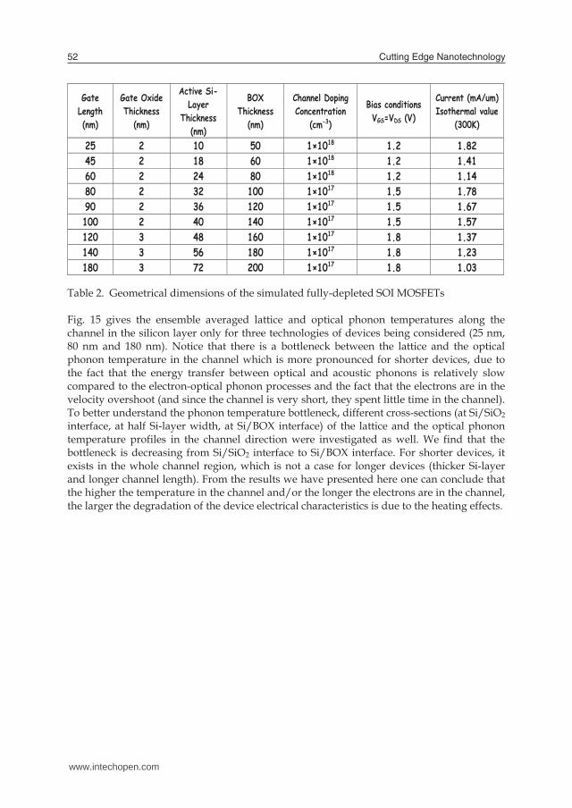
Cutting Edge Nanotechnology52
Gate Length (nm)
Gate Oxide Thickness
(nm)
Active Si-Layer
Thickness (nm)
BOX Thickness
(nm)
Channel Doping Concentration
(cm-3)
Bias conditions VGS=VDS (V)
Current (mA/um) Isothermal value
(300K)
25 2 10 50 1×10¹⁸ 1.2 1.82 45 2 18 60 1×10¹⁸ 1.2 1.41 60 2 24 80 1×10¹⁸ 1.2 1.14 80 2 32 100 1×10¹⁷ 1.5 1.78 90 2 36 120 1×10¹⁷ 1.5 1.67 100 2 40 140 1×10¹⁷ 1.5 1.57 120 3 48 160 1×10¹⁷ 1.8 1.37 140 3 56 180 1×10¹⁷ 1.8 1.23 180 3 72 200 1×10¹⁷ 1.8 1.03
Table 2. Geometrical dimensions of the simulated fully-depleted SOI MOSFETs Fig. 15 gives the ensemble averaged lattice and optical phonon temperatures along the channel in the silicon layer only for three technologies of devices being considered (25 nm, 80 nm and 180 nm). Notice that there is a bottleneck between the lattice and the optical phonon temperature in the channel which is more pronounced for shorter devices, due to the fact that the energy transfer between optical and acoustic phonons is relatively slow compared to the electron-optical phonon processes and the fact that the electrons are in the velocity overshoot (and since the channel is very short, they spent little time in the channel). To better understand the phonon temperature bottleneck, different cross-sections (at Si/SiO2 interface, at half Si-layer width, at Si/BOX interface) of the lattice and the optical phonon temperature profiles in the channel direction were investigated as well. We find that the bottleneck is decreasing from Si/SiO2 interface to Si/BOX interface. For shorter devices, it exists in the whole channel region, which is not a case for longer devices (thicker Si-layer and longer channel length). From the results we have presented here one can conclude that the higher the temperature in the channel and/or the longer the electrons are in the channel, the larger the degradation of the device electrical characteristics is due to the heating effects.
25 nm FD SOI nMOSFET Vgs=Vds=1.2V
45 nm FD SOI nMOSFET Vgs=Vds=1.2V
60nm FD SOI nMOSFET Vgs=Vds=1.2V Type of
simulation
Gate Electrode Temperature (K)
Current (mA/um)
Current Decrease (%)
Current (mA/um)
Current Decrease (%)
Current (mA/um)
Current Decrease (%)
isothermal 300 1.929 \ 1.5645 \ 1.2457 \ thermal 300 1.8176 5.78 1.4717 5.93 1.1885 4.73 thermal 400 1.7467 9.45 1.3957 10.79 1.1124 10.83 thermal 600 1.5997 17.1 1.2612 19.39 0.9882 20.79
80 nm FD SOI nMOSFET Vgs=Vds=1.5V
90 nm FD SOI nMOSFET Vgs=Vds=1.5V
100 nm FD SOI nMOSFET Vgs=Vds=1.5V Type of
simulation
Gate Electrode Temperature (K)
Current (mA/um)
Current Decrease (%)
Current (mA/um)
Current Decrease (%)
Current (mA/um)
Current Decrease (%)
isothermal 300 1.7810 \ 1.6671 \ 1.5743 \ thermal 300 1.5850 11 1.4805 11.19 1.4004 11.05 thermal 400 1.4612 17.96 1.3678 17.95 1.2833 18.48 thermal 600 1.2571 29.42 1.1784 29.31 1.1158 29.12
120 nm FD SOI nMOSFET Vgs=Vds=1.8V
140 nm FD SOI nMOSFET Vgs=Vds=1.8V
180 nm FD SOI nMOSFET Vgs=Vds=1.8V Type of
simulation
Gate Electrode Temperature (K)
Current (mA/um)
Current Decrease (%)
Current (mA/um)
Current Decrease (%)
Current (mA/um)
Current Decrease (%)
isothermal 300 1.3657 \ 1.2341 \ 1.0321 \ thermal 300 1.1439 16.34 1.0416 15.6 0.8570 15.22 thermal 400 1.0630 22.16 0.9654 21.85 0.8100 21.52 thermal 600 0.9256 32.22 0.8311 32.27 0.6940 32.76
Table 3. Current decrease with gate temperature for different FD SOI technologies.
5. Open Problems
From the discussion presented so far, we might conclude that device simulation without lattice heating has reached high levels of sophistication even in the quantum domain area. The inclusion of lattice heating is done using the energy balance picture by the group from Arizona State University or by including the heat flux term that accounts for the number of generated acoustic and optical phonons in a given mode.
www.intechopen.com
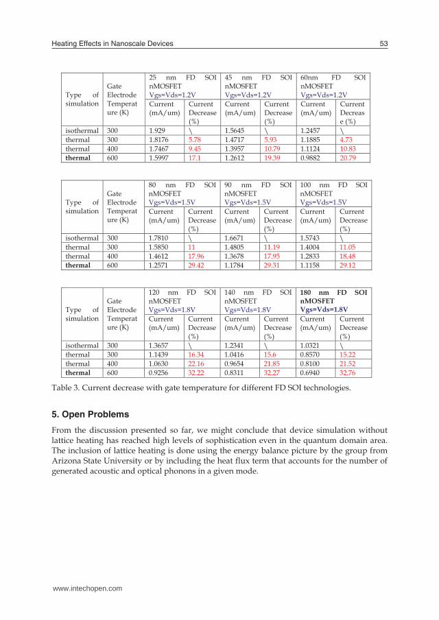
Heating Effects in Nanoscale Devices 53
Gate Length (nm)
Gate Oxide Thickness
(nm)
Active Si-Layer
Thickness (nm)
BOX Thickness
(nm)
Channel Doping Concentration
(cm-3)
Bias conditions VGS=VDS (V)
Current (mA/um) Isothermal value
(300K)
25 2 10 50 1×10¹⁸ 1.2 1.82 45 2 18 60 1×10¹⁸ 1.2 1.41 60 2 24 80 1×10¹⁸ 1.2 1.14 80 2 32 100 1×10¹⁷ 1.5 1.78 90 2 36 120 1×10¹⁷ 1.5 1.67 100 2 40 140 1×10¹⁷ 1.5 1.57 120 3 48 160 1×10¹⁷ 1.8 1.37 140 3 56 180 1×10¹⁷ 1.8 1.23 180 3 72 200 1×10¹⁷ 1.8 1.03
Table 2. Geometrical dimensions of the simulated fully-depleted SOI MOSFETs Fig. 15 gives the ensemble averaged lattice and optical phonon temperatures along the channel in the silicon layer only for three technologies of devices being considered (25 nm, 80 nm and 180 nm). Notice that there is a bottleneck between the lattice and the optical phonon temperature in the channel which is more pronounced for shorter devices, due to the fact that the energy transfer between optical and acoustic phonons is relatively slow compared to the electron-optical phonon processes and the fact that the electrons are in the velocity overshoot (and since the channel is very short, they spent little time in the channel). To better understand the phonon temperature bottleneck, different cross-sections (at Si/SiO2 interface, at half Si-layer width, at Si/BOX interface) of the lattice and the optical phonon temperature profiles in the channel direction were investigated as well. We find that the bottleneck is decreasing from Si/SiO2 interface to Si/BOX interface. For shorter devices, it exists in the whole channel region, which is not a case for longer devices (thicker Si-layer and longer channel length). From the results we have presented here one can conclude that the higher the temperature in the channel and/or the longer the electrons are in the channel, the larger the degradation of the device electrical characteristics is due to the heating effects.
25 nm FD SOI nMOSFET Vgs=Vds=1.2V
45 nm FD SOI nMOSFET Vgs=Vds=1.2V
60nm FD SOI nMOSFET Vgs=Vds=1.2V Type of
simulation
Gate Electrode Temperature (K)
Current (mA/um)
Current Decrease (%)
Current (mA/um)
Current Decrease (%)
Current (mA/um)
Current Decrease (%)
isothermal 300 1.929 \ 1.5645 \ 1.2457 \ thermal 300 1.8176 5.78 1.4717 5.93 1.1885 4.73 thermal 400 1.7467 9.45 1.3957 10.79 1.1124 10.83 thermal 600 1.5997 17.1 1.2612 19.39 0.9882 20.79
80 nm FD SOI nMOSFET Vgs=Vds=1.5V
90 nm FD SOI nMOSFET Vgs=Vds=1.5V
100 nm FD SOI nMOSFET Vgs=Vds=1.5V Type of
simulation
Gate Electrode Temperature (K)
Current (mA/um)
Current Decrease (%)
Current (mA/um)
Current Decrease (%)
Current (mA/um)
Current Decrease (%)
isothermal 300 1.7810 \ 1.6671 \ 1.5743 \ thermal 300 1.5850 11 1.4805 11.19 1.4004 11.05 thermal 400 1.4612 17.96 1.3678 17.95 1.2833 18.48 thermal 600 1.2571 29.42 1.1784 29.31 1.1158 29.12
120 nm FD SOI nMOSFET Vgs=Vds=1.8V
140 nm FD SOI nMOSFET Vgs=Vds=1.8V
180 nm FD SOI nMOSFET Vgs=Vds=1.8V Type of
simulation
Gate Electrode Temperature (K)
Current (mA/um)
Current Decrease (%)
Current (mA/um)
Current Decrease (%)
Current (mA/um)
Current Decrease (%)
isothermal 300 1.3657 \ 1.2341 \ 1.0321 \ thermal 300 1.1439 16.34 1.0416 15.6 0.8570 15.22 thermal 400 1.0630 22.16 0.9654 21.85 0.8100 21.52 thermal 600 0.9256 32.22 0.8311 32.27 0.6940 32.76
Table 3. Current decrease with gate temperature for different FD SOI technologies.
5. Open Problems
From the discussion presented so far, we might conclude that device simulation without lattice heating has reached high levels of sophistication even in the quantum domain area. The inclusion of lattice heating is done using the energy balance picture by the group from Arizona State University or by including the heat flux term that accounts for the number of generated acoustic and optical phonons in a given mode.
www.intechopen.com
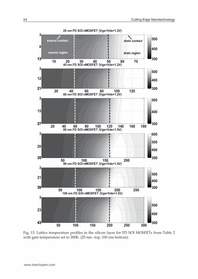
Cutting Edge Nanotechnology54
25 nm FD SOI nMOSFET (Vgs=Vds=1.2V)
10 20 30 40 50 60 70
3
8
131345 nm FD SOI nMOSFET (Vgs=Vds=1.2V)
20 40 60 80 100 120
3
12
212160 nm FD SOI nMOSFET (Vgs=Vds=1.2V)
20 40 60 80 100 120 140 160 180
3
15
2727
300
400
500
300
400
500
300
400
500
source contact drain contact
source region drain region
80 nm FD SOI nMOSFET (Vgs=Vds=1.5V)
50 100 150 200
3
20
353590 nm FD SOI nMOSFET (Vgs=Vds=1.5V)
50 100 150 200 250
3
21
3939100 nm FD SOI nMOSFET (Vgs=Vds=1.5V)
50 100 150 200 250 300
3
23
4343
300
400
500
600
300400
500
300
400
500
Fig. 13. Lattice temperature profiles in the silicon layer for FD SOI MOSFETs from Table 2 with gate temperature set to 300K. (25 nm –top, 100 nm-bottom).
25 nm FD SOI nMOSFET (Vgs=Vds=1.2V)
10 20 30 40 50 60 70
3
8
131345 nm FD SOI nMOSFET (Vgs=Vds=1.2V)
20 40 60 80 100 120
3
12
212160 nm FD SOI nMOSFET (Vgs=Vds=1.2V)
20 40 60 80 100 120 140 160 180
3
15
2727 300
400
500
300
400
500
300
400
500
600source contact drain contact
80 nm FD SOI nMOSFET (Vgs=Vds=1.5V)
50 100 150 200
3
20
353590 nm FD SOI nMOSFET (Vgs=Vds=1.5V)
50 100 150 200 250
3
21
3939100 nm FD SOI nMOSFET (Vgs=Vds=1.5V)
50 100 150 200 250 300
3
23
4343 300
400
500
600
400
600
300
400500600
Fig. 14. Lattice temperature profile in silicon layer for different device geometries of fully-depleted SOI MOSFET when gate temperature is set to 400K.
www.intechopen.com
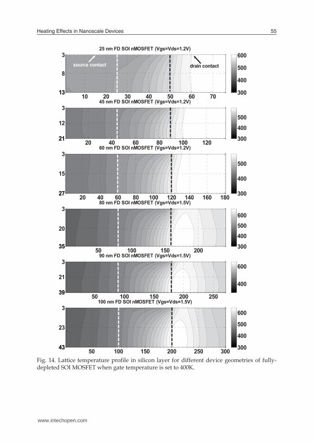
Heating Effects in Nanoscale Devices 55
25 nm FD SOI nMOSFET (Vgs=Vds=1.2V)
10 20 30 40 50 60 70
3
8
131345 nm FD SOI nMOSFET (Vgs=Vds=1.2V)
20 40 60 80 100 120
3
12
212160 nm FD SOI nMOSFET (Vgs=Vds=1.2V)
20 40 60 80 100 120 140 160 180
3
15
2727
300
400
500
300
400
500
300
400
500
source contact drain contact
source region drain region
80 nm FD SOI nMOSFET (Vgs=Vds=1.5V)
50 100 150 200
3
20
353590 nm FD SOI nMOSFET (Vgs=Vds=1.5V)
50 100 150 200 250
3
21
3939100 nm FD SOI nMOSFET (Vgs=Vds=1.5V)
50 100 150 200 250 300
3
23
4343
300
400
500
600
300400
500
300
400
500
Fig. 13. Lattice temperature profiles in the silicon layer for FD SOI MOSFETs from Table 2 with gate temperature set to 300K. (25 nm –top, 100 nm-bottom).
25 nm FD SOI nMOSFET (Vgs=Vds=1.2V)
10 20 30 40 50 60 70
3
8
131345 nm FD SOI nMOSFET (Vgs=Vds=1.2V)
20 40 60 80 100 120
3
12
212160 nm FD SOI nMOSFET (Vgs=Vds=1.2V)
20 40 60 80 100 120 140 160 180
3
15
2727 300
400
500
300
400
500
300
400
500
600source contact drain contact
80 nm FD SOI nMOSFET (Vgs=Vds=1.5V)
50 100 150 200
3
20
353590 nm FD SOI nMOSFET (Vgs=Vds=1.5V)
50 100 150 200 250
3
21
3939100 nm FD SOI nMOSFET (Vgs=Vds=1.5V)
50 100 150 200 250 300
3
23
4343 300
400
500
600
400
600
300
400500600
Fig. 14. Lattice temperature profile in silicon layer for different device geometries of fully-depleted SOI MOSFET when gate temperature is set to 400K.
www.intechopen.com
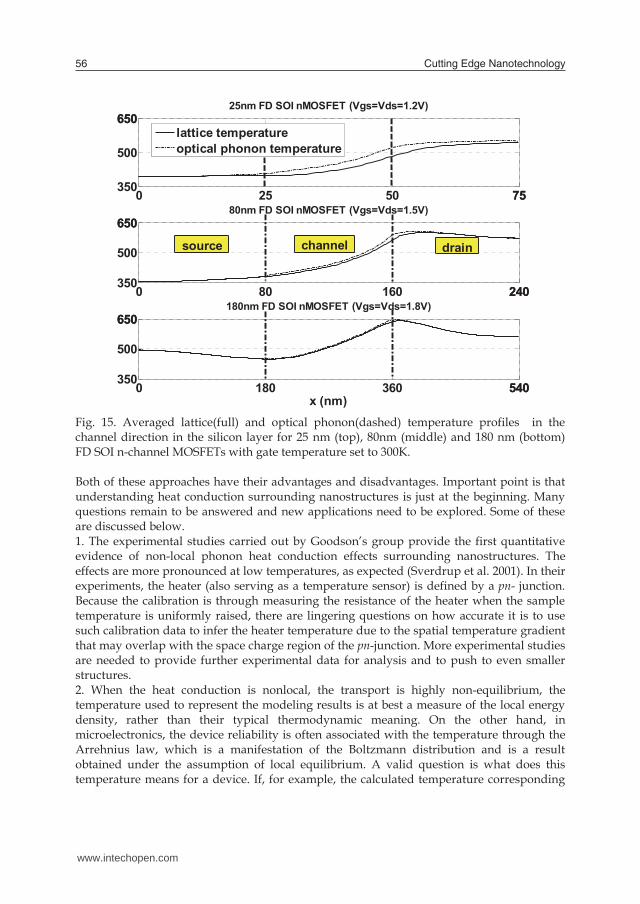
Cutting Edge Nanotechnology56
0 25 50 7575350
500
65065025nm FD SOI nMOSFET (Vgs=Vds=1.2V)
0 80 160 240240350
500
65065080nm FD SOI nMOSFET (Vgs=Vds=1.5V)
0 180 360 540540350
500
650650
x (nm)
180nm FD SOI nMOSFET (Vgs=Vds=1.8V)
lattice temperatureoptical phonon temperature
source channel drain
Fig. 15. Averaged lattice(full) and optical phonon(dashed) temperature profiles in the channel direction in the silicon layer for 25 nm (top), 80nm (middle) and 180 nm (bottom) FD SOI n-channel MOSFETs with gate temperature set to 300K. Both of these approaches have their advantages and disadvantages. Important point is that understanding heat conduction surrounding nanostructures is just at the beginning. Many questions remain to be answered and new applications need to be explored. Some of these are discussed below. 1. The experimental studies carried out by Goodson’s group provide the first quantitative evidence of non-local phonon heat conduction effects surrounding nanostructures. The effects are more pronounced at low temperatures, as expected (Sverdrup et al. 2001). In their experiments, the heater (also serving as a temperature sensor) is defined by a pn- junction. Because the calibration is through measuring the resistance of the heater when the sample temperature is uniformly raised, there are lingering questions on how accurate it is to use such calibration data to infer the heater temperature due to the spatial temperature gradient that may overlap with the space charge region of the pn-junction. More experimental studies are needed to provide further experimental data for analysis and to push to even smaller structures. 2. When the heat conduction is nonlocal, the transport is highly non-equilibrium, the temperature used to represent the modeling results is at best a measure of the local energy density, rather than their typical thermodynamic meaning. On the other hand, in microelectronics, the device reliability is often associated with the temperature through the Arrehnius law, which is a manifestation of the Boltzmann distribution and is a result obtained under the assumption of local equilibrium. A valid question is what does this temperature means for a device. If, for example, the calculated temperature corresponding
to the local energy density reaches the melting point, does it mean that local melting occur? The molecular dynamics simulations may shed some light on this question, as is discussed in Goodson et al.’s paper [Asheghi et al., 1998]. 3. The simulations so far are based on either Monte Carlo methods or the Boltzmann equation and take the various relaxation times as input parameters. These parameters are subject to a wide range of uncertainties. The phonon relaxation time, for example, were mostly derived from the modeling work in the 1950s and 1960s on the thermal conductivity of bulk materials. The relaxation time in these models is often obtained under various approximations, such as the Debye model for the phonon dispersion. There are many variables in these past models that can lead to different values of the relaxation time. There is a clear need for more accurate information on the relaxation times. Molecular dynamics simulation may be one way to obtain them. Similarly, electron-phonon scattering processes also need further consideration, particularly when electrons have very different temperatures from that of phonons. 4. In addition to the different application problems in microelectronics and in data storage, there are also new fundamental problems associated with nonlocal heat conduction. Past studies have considered phonons only. The concurrent electron and phonon nonlocal transport and nonequilibrium transport is an example. A recent proposal is to use the departure from equilibrium between electrons and phonons at a small contact point as a means to increase the thermoelectric energy conversion efficiency (Goshal et al., 2002). The transport in this case can well become nonlocal for both electrons and phonons. This possibility was raised, but has never been studied (Chen, 1996). 5. The above examples emphasize the small length scales involved in nano-devices and nanomaterials. Short time scales are also becoming increasingly important. Similar questions can be raised for transport at short time scales as for the small length scales. Lasers can deliver a pulse as short as a few femtoseconds (1 fs = 10-15 s). Energy transduction mechanisms at such short time scales can differ significantly from that at macroscale. Microelectronic devices are pushing to the tens of gigaherts clock frequency with a much shorter transient time. The device temperature rise in such short time scales can be very different from predictions of the Fourier law.
6. References
Ahmed, S. S. (2005) . Ph.D. Thesis, Arizona State University, Advisor: Prof. D. Vasileska. Artaki, M. & Price, P. J. (1989). Hot phonon effects in silicon field-effect-transistors, J. Appl.
Phys. Vol. 65, 1989, pp. 1317-1320. Asheghi, M.; Touzelbaev, M.N.; Goodson, K.E.; Leung, Y.K. & Wong, S.S. (1998).
Temperature Dependent Thermal Conductivity of Single-Crystal Silicon Layers in SOI Substrates, ASME Journal of Heat Transfer, Vol.120, 1998, pp. 30-33.
Asheghi, M.; Touzelbaev, M. N.; Goodson, K. E.; Leung, Y. K.; & Wong, S. S. (1998). Temperature Dependent Thermal Conductivity of Single-Crystal Silicon Layers in SOI Substrates, ASME Journal of Heat Transfer, Vol.120, 1998, pp. 30-33.
Borkar, S. (1999). Design Challenges of Technology Scaling, IEEE Micro, Vol. 19, 1999, pp. 23-29.
Cercignani, C. (1998). The Boltzmann Equation and its Applications, Vol. 67 of Applied Mathematical Sciences, Springer-Verlag, 1988.
www.intechopen.com
Heating Effects in Nanoscale Devices 57
0 25 50 7575350
500
65065025nm FD SOI nMOSFET (Vgs=Vds=1.2V)
0 80 160 240240350
500
65065080nm FD SOI nMOSFET (Vgs=Vds=1.5V)
0 180 360 540540350
500
650650
x (nm)
180nm FD SOI nMOSFET (Vgs=Vds=1.8V)
lattice temperatureoptical phonon temperature
source channel drain
Fig. 15. Averaged lattice(full) and optical phonon(dashed) temperature profiles in the channel direction in the silicon layer for 25 nm (top), 80nm (middle) and 180 nm (bottom) FD SOI n-channel MOSFETs with gate temperature set to 300K. Both of these approaches have their advantages and disadvantages. Important point is that understanding heat conduction surrounding nanostructures is just at the beginning. Many questions remain to be answered and new applications need to be explored. Some of these are discussed below. 1. The experimental studies carried out by Goodson’s group provide the first quantitative evidence of non-local phonon heat conduction effects surrounding nanostructures. The effects are more pronounced at low temperatures, as expected (Sverdrup et al. 2001). In their experiments, the heater (also serving as a temperature sensor) is defined by a pn- junction. Because the calibration is through measuring the resistance of the heater when the sample temperature is uniformly raised, there are lingering questions on how accurate it is to use such calibration data to infer the heater temperature due to the spatial temperature gradient that may overlap with the space charge region of the pn-junction. More experimental studies are needed to provide further experimental data for analysis and to push to even smaller structures. 2. When the heat conduction is nonlocal, the transport is highly non-equilibrium, the temperature used to represent the modeling results is at best a measure of the local energy density, rather than their typical thermodynamic meaning. On the other hand, in microelectronics, the device reliability is often associated with the temperature through the Arrehnius law, which is a manifestation of the Boltzmann distribution and is a result obtained under the assumption of local equilibrium. A valid question is what does this temperature means for a device. If, for example, the calculated temperature corresponding
to the local energy density reaches the melting point, does it mean that local melting occur? The molecular dynamics simulations may shed some light on this question, as is discussed in Goodson et al.’s paper [Asheghi et al., 1998]. 3. The simulations so far are based on either Monte Carlo methods or the Boltzmann equation and take the various relaxation times as input parameters. These parameters are subject to a wide range of uncertainties. The phonon relaxation time, for example, were mostly derived from the modeling work in the 1950s and 1960s on the thermal conductivity of bulk materials. The relaxation time in these models is often obtained under various approximations, such as the Debye model for the phonon dispersion. There are many variables in these past models that can lead to different values of the relaxation time. There is a clear need for more accurate information on the relaxation times. Molecular dynamics simulation may be one way to obtain them. Similarly, electron-phonon scattering processes also need further consideration, particularly when electrons have very different temperatures from that of phonons. 4. In addition to the different application problems in microelectronics and in data storage, there are also new fundamental problems associated with nonlocal heat conduction. Past studies have considered phonons only. The concurrent electron and phonon nonlocal transport and nonequilibrium transport is an example. A recent proposal is to use the departure from equilibrium between electrons and phonons at a small contact point as a means to increase the thermoelectric energy conversion efficiency (Goshal et al., 2002). The transport in this case can well become nonlocal for both electrons and phonons. This possibility was raised, but has never been studied (Chen, 1996). 5. The above examples emphasize the small length scales involved in nano-devices and nanomaterials. Short time scales are also becoming increasingly important. Similar questions can be raised for transport at short time scales as for the small length scales. Lasers can deliver a pulse as short as a few femtoseconds (1 fs = 10-15 s). Energy transduction mechanisms at such short time scales can differ significantly from that at macroscale. Microelectronic devices are pushing to the tens of gigaherts clock frequency with a much shorter transient time. The device temperature rise in such short time scales can be very different from predictions of the Fourier law.
6. References
Ahmed, S. S. (2005) . Ph.D. Thesis, Arizona State University, Advisor: Prof. D. Vasileska. Artaki, M. & Price, P. J. (1989). Hot phonon effects in silicon field-effect-transistors, J. Appl.
Phys. Vol. 65, 1989, pp. 1317-1320. Asheghi, M.; Touzelbaev, M.N.; Goodson, K.E.; Leung, Y.K. & Wong, S.S. (1998).
Temperature Dependent Thermal Conductivity of Single-Crystal Silicon Layers in SOI Substrates, ASME Journal of Heat Transfer, Vol.120, 1998, pp. 30-33.
Asheghi, M.; Touzelbaev, M. N.; Goodson, K. E.; Leung, Y. K.; & Wong, S. S. (1998). Temperature Dependent Thermal Conductivity of Single-Crystal Silicon Layers in SOI Substrates, ASME Journal of Heat Transfer, Vol.120, 1998, pp. 30-33.
Borkar, S. (1999). Design Challenges of Technology Scaling, IEEE Micro, Vol. 19, 1999, pp. 23-29.
Cercignani, C. (1998). The Boltzmann Equation and its Applications, Vol. 67 of Applied Mathematical Sciences, Springer-Verlag, 1988.
www.intechopen.com
Cutting Edge Nanotechnology58
Chen, G. (1996). J.Heat Transf., Vol. 118, 1996, pp. 539- . Chen, G. (2001). Ballistic-Diffusive Heat-Conduction Equations, Physical Review Letters, Vol.
86, 2001, pp. 2297-2300. Chen, G. & Shakouri, A. (2002). Nanoengineered Structures for Solid-State Energy
Conversion, Transactions of the ASME, Vol. 124, 2002, pp. 242-252. Choi, S.-H.; Maruyama, S. (2003). Evaluation of the phonon mean free path in thin films by
using classical molecular dynamics, Journal of the Korean Physical Society, Vol. 43, 2003, pp. 747-753.
Ferry, D. K. (2000). Semiconductor Transport, New York: Taylor & Francis, 2000. Gaur, S. P. & Navon, D. H. (1976). Two-dimensional carrier flow in a transistor structure under
non-isothermal conditions, IEEE Trans. Electron Devices, Vol. 23, 1976, pp. 50-57. Geppert, L. (1999). Solid state [semiconductors. 1999 technology analysis and forecast],
Spectrum, IEEE, Vol. 36, 1999, pp. 52-56. Goshal, U. et al. (2002). , Appl. Phys. Lett.,Vol. 80, 1976,pp. 3006- He, X. (1999). MS Thesis, Arizona State University, 1999, Advisor: Prof. D. Vasileska. Ju, Y. S. & Goodson, K. E. (1999). Phonon Scattering in Silicon Films with Thickness of Order
100 nm, Applied Physics Letters, Vol. 74, 1999, pp. 3005-3007. Lai, J. & Majumdar, A. (1996). Concurent thermal and electrical modeling of submicrometer
silicon devices, J. Appl. Phys. , Vol. 79, 1996, pp. 7353- . Leung, Y. K.; Paul, A. K.; Goodson,K. E.; Plummer, J. D. & Wong, S.S. (1997). Heating
mechanisms of LDMOS and LIGBT in ultrathin SOI, IEEE Electron Device Lett., Vol. 18, 1997, pp. 414-
Liu, W. & Asheghi, M. (2004). Phonon-Boundary Scattering in Ultra Thin Single-Crystal Silicon Layers, Applied Physics Letters, Vol. 84, 2004, pp. 3819-3821.
a Liu, W. & Asheghi, M. (2005). Thermal Conductivity of Ultra-Thin Single Crystal Silicon Layers, Journal of Heat Transfer, Vol. 128, 2005, pp. 75-83.
b Liu, W.; & Asheghi, M. (2005). J. Appl. Phys., Vol. 98, 2005, 123523-1. Majumdar, A. (1993). Microscale Heat Conduction in Dielectric Thin Films, Journal of Heat
Transfer, Vol. 115, 1993, pp.7-16. Majumdar, A.; Fushinobu, K. & Hijikata, K. (1995). Effect of hate voltage on hot electron and
hot phonon interaction and transport in a submicrometer transistor, J. Appl. Phys. Vol. 77, 1995, pp. 6686- .
Narumanchi, S. V. J.; Murthy, J. Y. & Amon, C. H. (2004). Submicron heat transport model in silicon accounting for phonon dispersion and polarization, Transactions of the ASME, Vol. 126, 2004, pp. 946-955.
Palankovski, V. & Selberherr, S. (2001). Micro materials modeling in MINIMOS-NT, Journal Microsystem Technologies, Vol. 7, November 2001, pp. 183-187.
Pop, E.; Sinha, S. & Goodson, K. E. (2006) “Heat genareation and transport in nanometer-scale transistors”, Proceedings of the IEEE, Vol. 94, 2006, pp. 1587-1601.
Raleva, K.; Vasileska, D.; Goodnick, S. M. & Dzekov T. (2008). Modeling thermal effects in nano-devices, Journal of Computational Electronics, DOI 10.1007/s10825-008-0189-3 © Springer Science+Business Media LLC 2008, J. Computational Electronics, Vol. 7, 2008, pp. 226-230.
Reif, F. (1985). Fundamentals of Statistical and Thermal Physics , McGraw-Hill, London, 1985.
Sadi, T. Kelsall, R.W. & Pilgrim, N. J. (2007) "Electrothermal Monte Carlo Simulation of Submicrometer Si/SiGe MODFETs", IEEE Trans. on Electron Devices, Vol.54, No.2, February 2007, pp. -
Silvaco Manual (www.silvaco.com). Shakouri, A.; Lee, E. Y.; Smith, D. L.; Narayanamurti, V. & Bowers, J. E. (1998).
Thermoelectric Effects in Submicron Heterostructure Barriers, Microscale Thermophysical Engineering, Vol. 2, 1998, pp. 37-47.
Sondheimer, E. H. (2001). The Mean Free Path of Electrons in Metals, Advances in Physics, Vol. 1, no. 1, Jan. 1952, reprinted in Advances in Physics, Vol. 50, 2001, pp. 499-537.
Sridharan, S.; Venkatachalam, A. & Yoder P. D. (2008). Electrothermal analysis of AlGaN/GaN high electron mobility transistors, Journ. of Compt. Electronics Vol. 7, 2008, 236–239.
Sverdrup, P. G.; Sinha, S.; Uma, S.; Asheghi, M. & . Goodson, K. E. (2001). App. Phys. Let. Vol. 78, 2001, pp. 3331 -.
Tien, C. L.; Majumdar, A. & Gerner, F. M. (1998). Microscale Energy Transport, Taylor&Francis, 1998.
Vasileska,D.; Raleva, K. &. Goodnick, S. M. (2008). Modeling heating effects in nanoscale devices: the present and the future, Journal of Comp. Electronics, DOI 10.1007/s10825-008-0254-y, 2008.
Vasileska, Raleva and Goodnick, S.M. Self-Heating Effects in Nano-Scale FD SOI Devices: The Role of the Substrate, Boundary Conditions at Various Interfaces and the Dielectric Material Type for the BOX, IEEE Trans. Electron Devices, Vol. 56, No. 12, pp. 3064-3071 (2009).
Wachutka, G.K. (1990). Rigorous Thermodynamic Treatment of Heat Generation and Conduction in Semiconductor Device Modeling, IEEE Trans. Comp. Aided Design, Vol 11, 1990, pp 1141-1149.
Zeng, G.; Fan, X.; LaBounty, C.; Croke, E.; Zhang, Y.; Christofferson, J.; Vashaee, D.; Shakouri, A. & Bowers, J.E. (2003). Cooling Power Density of SiGe/Si Superlattice Micro Refrigerators, Materials Research Society Fall Meeting 2003, Proceedings Vol. 793, paper S2.2, December 2003, Boston, MA.
www.intechopen.com
Heating Effects in Nanoscale Devices 59
Chen, G. (1996). J.Heat Transf., Vol. 118, 1996, pp. 539- . Chen, G. (2001). Ballistic-Diffusive Heat-Conduction Equations, Physical Review Letters, Vol.
86, 2001, pp. 2297-2300. Chen, G. & Shakouri, A. (2002). Nanoengineered Structures for Solid-State Energy
Conversion, Transactions of the ASME, Vol. 124, 2002, pp. 242-252. Choi, S.-H.; Maruyama, S. (2003). Evaluation of the phonon mean free path in thin films by
using classical molecular dynamics, Journal of the Korean Physical Society, Vol. 43, 2003, pp. 747-753.
Ferry, D. K. (2000). Semiconductor Transport, New York: Taylor & Francis, 2000. Gaur, S. P. & Navon, D. H. (1976). Two-dimensional carrier flow in a transistor structure under
non-isothermal conditions, IEEE Trans. Electron Devices, Vol. 23, 1976, pp. 50-57. Geppert, L. (1999). Solid state [semiconductors. 1999 technology analysis and forecast],
Spectrum, IEEE, Vol. 36, 1999, pp. 52-56. Goshal, U. et al. (2002). , Appl. Phys. Lett.,Vol. 80, 1976,pp. 3006- He, X. (1999). MS Thesis, Arizona State University, 1999, Advisor: Prof. D. Vasileska. Ju, Y. S. & Goodson, K. E. (1999). Phonon Scattering in Silicon Films with Thickness of Order
100 nm, Applied Physics Letters, Vol. 74, 1999, pp. 3005-3007. Lai, J. & Majumdar, A. (1996). Concurent thermal and electrical modeling of submicrometer
silicon devices, J. Appl. Phys. , Vol. 79, 1996, pp. 7353- . Leung, Y. K.; Paul, A. K.; Goodson,K. E.; Plummer, J. D. & Wong, S.S. (1997). Heating
mechanisms of LDMOS and LIGBT in ultrathin SOI, IEEE Electron Device Lett., Vol. 18, 1997, pp. 414-
Liu, W. & Asheghi, M. (2004). Phonon-Boundary Scattering in Ultra Thin Single-Crystal Silicon Layers, Applied Physics Letters, Vol. 84, 2004, pp. 3819-3821.
a Liu, W. & Asheghi, M. (2005). Thermal Conductivity of Ultra-Thin Single Crystal Silicon Layers, Journal of Heat Transfer, Vol. 128, 2005, pp. 75-83.
b Liu, W.; & Asheghi, M. (2005). J. Appl. Phys., Vol. 98, 2005, 123523-1. Majumdar, A. (1993). Microscale Heat Conduction in Dielectric Thin Films, Journal of Heat
Transfer, Vol. 115, 1993, pp.7-16. Majumdar, A.; Fushinobu, K. & Hijikata, K. (1995). Effect of hate voltage on hot electron and
hot phonon interaction and transport in a submicrometer transistor, J. Appl. Phys. Vol. 77, 1995, pp. 6686- .
Narumanchi, S. V. J.; Murthy, J. Y. & Amon, C. H. (2004). Submicron heat transport model in silicon accounting for phonon dispersion and polarization, Transactions of the ASME, Vol. 126, 2004, pp. 946-955.
Palankovski, V. & Selberherr, S. (2001). Micro materials modeling in MINIMOS-NT, Journal Microsystem Technologies, Vol. 7, November 2001, pp. 183-187.
Pop, E.; Sinha, S. & Goodson, K. E. (2006) “Heat genareation and transport in nanometer-scale transistors”, Proceedings of the IEEE, Vol. 94, 2006, pp. 1587-1601.
Raleva, K.; Vasileska, D.; Goodnick, S. M. & Dzekov T. (2008). Modeling thermal effects in nano-devices, Journal of Computational Electronics, DOI 10.1007/s10825-008-0189-3 © Springer Science+Business Media LLC 2008, J. Computational Electronics, Vol. 7, 2008, pp. 226-230.
Reif, F. (1985). Fundamentals of Statistical and Thermal Physics , McGraw-Hill, London, 1985.
Sadi, T. Kelsall, R.W. & Pilgrim, N. J. (2007) "Electrothermal Monte Carlo Simulation of Submicrometer Si/SiGe MODFETs", IEEE Trans. on Electron Devices, Vol.54, No.2, February 2007, pp. -
Silvaco Manual (www.silvaco.com). Shakouri, A.; Lee, E. Y.; Smith, D. L.; Narayanamurti, V. & Bowers, J. E. (1998).
Thermoelectric Effects in Submicron Heterostructure Barriers, Microscale Thermophysical Engineering, Vol. 2, 1998, pp. 37-47.
Sondheimer, E. H. (2001). The Mean Free Path of Electrons in Metals, Advances in Physics, Vol. 1, no. 1, Jan. 1952, reprinted in Advances in Physics, Vol. 50, 2001, pp. 499-537.
Sridharan, S.; Venkatachalam, A. & Yoder P. D. (2008). Electrothermal analysis of AlGaN/GaN high electron mobility transistors, Journ. of Compt. Electronics Vol. 7, 2008, 236–239.
Sverdrup, P. G.; Sinha, S.; Uma, S.; Asheghi, M. & . Goodson, K. E. (2001). App. Phys. Let. Vol. 78, 2001, pp. 3331 -.
Tien, C. L.; Majumdar, A. & Gerner, F. M. (1998). Microscale Energy Transport, Taylor&Francis, 1998.
Vasileska,D.; Raleva, K. &. Goodnick, S. M. (2008). Modeling heating effects in nanoscale devices: the present and the future, Journal of Comp. Electronics, DOI 10.1007/s10825-008-0254-y, 2008.
Vasileska, Raleva and Goodnick, S.M. Self-Heating Effects in Nano-Scale FD SOI Devices: The Role of the Substrate, Boundary Conditions at Various Interfaces and the Dielectric Material Type for the BOX, IEEE Trans. Electron Devices, Vol. 56, No. 12, pp. 3064-3071 (2009).
Wachutka, G.K. (1990). Rigorous Thermodynamic Treatment of Heat Generation and Conduction in Semiconductor Device Modeling, IEEE Trans. Comp. Aided Design, Vol 11, 1990, pp 1141-1149.
Zeng, G.; Fan, X.; LaBounty, C.; Croke, E.; Zhang, Y.; Christofferson, J.; Vashaee, D.; Shakouri, A. & Bowers, J.E. (2003). Cooling Power Density of SiGe/Si Superlattice Micro Refrigerators, Materials Research Society Fall Meeting 2003, Proceedings Vol. 793, paper S2.2, December 2003, Boston, MA.
www.intechopen.com
Cutting Edge Nanotechnology60
www.intechopen.com
Cutting Edge NanotechnologyEdited by Dragica Vasileska
ISBN 978-953-7619-93-0Hard cover, 444 pagesPublisher InTechPublished online 01, March, 2010Published in print edition March, 2010
InTech EuropeUniversity Campus STeP Ri Slavka Krautzeka 83/A 51000 Rijeka, Croatia Phone: +385 (51) 770 447 Fax: +385 (51) 686 166www.intechopen.com
InTech ChinaUnit 405, Office Block, Hotel Equatorial Shanghai No.65, Yan An Road (West), Shanghai, 200040, China
Phone: +86-21-62489820 Fax: +86-21-62489821
The main purpose of this book is to describe important issues in various types of devices ranging fromconventional transistors (opening chapters of the book) to molecular electronic devices whose fabrication andoperation is discussed in the last few chapters of the book. As such, this book can serve as a guide foridentifications of important areas of research in micro, nano and molecular electronics. We deeplyacknowledge valuable contributions that each of the authors made in writing these excellent chapters.
How to referenceIn order to correctly reference this scholarly work, feel free to copy and paste the following:
Dragica Vasileska, Katerina Raleva and Stephen M. Goodnick (2010). Heating Effects in Nanoscale Devices,Cutting Edge Nanotechnology, Dragica Vasileska (Ed.), ISBN: 978-953-7619-93-0, InTech, Available from:http://www.intechopen.com/books/cutting-edge-nanotechnology/heating-effects-in-nanoscale-devices

© 2010 The Author(s). Licensee IntechOpen. This chapter is distributedunder the terms of the Creative Commons Attribution-NonCommercial-ShareAlike-3.0 License, which permits use, distribution and reproduction fornon-commercial purposes, provided the original is properly cited andderivative works building on this content are distributed under the samelicense.