Heated microcantilevers sensors
9
Slide # Heated microcantilevers sensors IR image of the cantilever Microcantilever with CNT sensing layers Heated microcantilever The heated cantilever can be used as an excellent sensor for (i) chemical analysis of trapped molecules in the CNT layers, (ii) measuring thermal properties of surrounding gases, and (iii) various SPM probing methods, including lithography
description
Heated microcantilevers sensors. Heated microcantilever. Microcantilever with CNT sensing layers. IR image of the cantilever. - PowerPoint PPT Presentation
Transcript of Heated microcantilevers sensors

Slide #
Heated microcantilevers sensors
IR image of the cantileverMicrocantilever with CNT sensing layers
Heated microcantilever
The heated cantilever can be used as an excellent sensor for (i) chemical analysis of trapped molecules in the CNT layers, (ii) measuring thermal properties of surrounding gases, and (iii) various SPM probing methods, including lithography
Slide #2
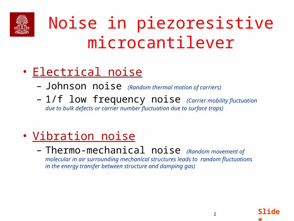
Noise in piezoresistive microcantilever
• Electrical noise– Johnson noise (Random thermal motion of carriers)
– 1/f low frequency noise (Carrier mobility fluctuation due to bulk defects or carrier number fluctuation due to surface traps)
• Vibration noise– Thermo-mechanical noise (Random movement of molecular in
air surrounding mechanical structures leads to random fluctuations in the energy transfer between structure and damping gas)

Slide #3
Johnson noise
TRkS BV 4SV: Noise power spectrum density
kB: Boltzmann's constant
T : Temperature
R : Resistance
pAR
fTkrms B
noiseI 89.34
R = 1100 Ω
Measurement bandwidth Δf = 1 Hz
Electrical noise
Deflection sensitivity = 11e-5 per µm, Vbias = 1.0 V
RMS noise JOHNSON = 0.03 nm

Slide #4
dfNf
Vrms
f
f
biasf
noiseI
2
1
2/1
1/f low frequency noise (Flicker noise)
SV : noise power spectral density [V2/Hz]
N : the number of carriers (depends on the piezoresistor volume and implant
dose)
Vbias : bias voltage , f : the frequency, n: unity (n=1)
α: empirical coefficient depends on annealing length:
fNf
VS
nbias
V
162 1018.2
)/ln(1018.21018.2
1216
162 2
1
ffdff
ef
fnoise
pARerms noiseI 1.302/
fmax= 100 Hz
fmin= 1 Hz
R = 99.2 Ω
Lr = 54 µm
Wr = 14 µm
Hr = 2 µm
Vbias = 1 V
µ = 400 cm2/Vs
kBT = 0.026 eV
α=1.0e-6
nbias
V Nf
VS
2
Electrical noise

Slide #5
Vibration noise
Thermo-mechanical noise
0
4
kTBQk
noiserms BTM
L=250 µm
W=140 µm
H=2 µm
E = 179GPa
Q = 69
w0 = 2*pi* 31.5 kHz
KBT = 0.026 eV
k= 3.11N/m
B = 1 Hz
RMS noise TM = 0.0013 nm
P. G. Datskos, N. V. Lavrik, and S. Rajic, “Performance of uncooled microcantilever thermal detectors”, Rev. Sci. Intr., 75, 1134 (2004)
Force noise spectrum density
At resonance:
)2/(4 0QfTkkS BF
At resonance, Vac = 5.0 sin (ωt)
nmrmsrmsrms noiseVibnoiseElecttotal 031.0)( 5.022
V
kQ
ZC
V
rms
ac
total 12
Minimum Δφ = 12 μV

Slide #
Nanowire based chemical sensing
6
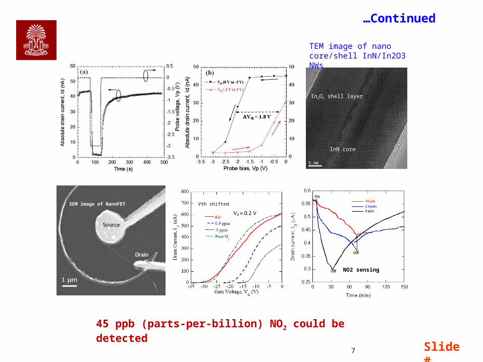
InN/In2O3 nano core/shell based FET sensor
J. Liu, Z. Cai, G. Koley, “Charge transport and trapping in InN nanowires investigated by scanning probe microscopy”, J. Appl. Phys. 106, 124907 (2009)
µ = 150 cm2
/Vs
SEM image
TEM image Diffraction pattern
Morphology Probe current
Slide #7
…Continued
45 ppb (parts-per-billion) NO2 could be detected
InN core
In2O3 shell layer
Vth shifted
TEM image of nano core/shell InN/In2O3 NWs
SEM image of NanoFET
NO2 sensing
Slide #8
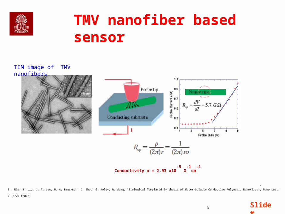
TMV nanofiber based sensor
Z. Niu, J. Liu, L. A. Lee, M. A. Bruckman, D. Zhao, G. Koley, Q. Wang, “Biological Templated Synthesis of Water-Soluble Conductive Polymeric Nanowires”, Nano Lett. 7, 3729 (2007)
Conductivity σ = 2.93 x10⁻⁵
Ω-1
cm-1
TEM image of TMV nanofibers

Slide #9
…Continued
M. A. Bruckman, J. Liu, G. Koley, Y. Li, B. Benicewicz, Z. Niu, and Q. Wang, “Tobacco mosaic virus based thin film sensor for detection of volatile organic compounds”, J. Mater. Chem. 20, 5715 (2010)
Good selectivity toward Methanol and Ethanol vapor
Methanol
On
Off
Time (s)