AMath Special Functions Reference Manual with Implementation ...

Hardware/Software Implementation of the Security Functions for Third Generation Cellular Networks
by
Tomás Balderas Contreras B.Sc., BUAP
A thesis submitted in partial fulfillment of the requirement for the degree of
MASTER OF SCIENCE IN COMPUTER SCIENCE
at
Instituto Nacional de Astrofísica, Óptica y Electrónica
December 2004 Tonantzintla, Puebla. MEXICO
Supervised by
Dr. René Armando Cumplido Parra Associate Researcher at INAOE
©INAOE 2004 All rights reserved
The author grants INAOE the right to reproduce and distribute full or partial copies of this dissertation

Abstract
The widespread use of third generation (3G) cellular communications networks will
revolutionize the way people communicate with each other and the manner in which
large and medium-size companies share their information and make businesses. The
most promising 3G technology, the Universal Mobile Telecommunications System
(UMTS) standard, offers advanced services, high transmission data rates (384 Kbps
– 2 Mbps) and an advanced security architecture based on a mutual authentication
protocol, a confidentiality algorithm (f8 ), an integrity algorithm (f9 ) and a block
ciphering algorithm (KASUMI). This dissertation meets the problem of efficiently
implementing the algorithms aforementioned and proposes a novel solution scheme
that achieves higher performance than the two traditional solution approaches: soft-
ware implementation in a general purpose microprocessor and the use of an external
coprocessor unit. The contributions of this project to its state of the art are multi-
fold. First, four different high performance hardware functional units implementing
the KASUMI block cipher, one of them reaching the highest throughput reported so
far. Second, the integration of one of such functional units into the microarchitec-
ture of a general purpose processor and the definition of new instructions to perform
encryption. Thus, the new solution approach is a combination of hardware and soft-
ware.

Resumen
El empleo cada vez mas difundido de las redes celulares de comunicacion de tercera
generacion (3G) promete revolucionar la manera en que la gente se comunica y la
forma en que las companıas, grandes y medianas, comparten su informacion y rea-
lizan actividades de negocios. El estandar de tercera generacion mas prometedor es
UMTS (Universal Mobile Telecommunications System) y ofrece una gama de servicios
avanzados, tasas de transmision elevadas (384 Kbps – 2 Mbps) y una arquitectura
de seguridad avanzada que cuenta con un protocolo para autenticacion mutua, un
algoritmo para confidencialidad (f8 ), un algoritmo para integridad (f9 ) y un algoritmo
para cifrado de bloques (KASUMI). El presente documento trata el problema de
implantar de forma eficiente los algoritmos mencionados anteriormente y propone
un esquema de solucion original que alcanza un mayor desempeno que los enfoques
tradicionales: implantacion en software para procesadores de proposito general y
el uso de unidades coprocesadoras externas al procesador central. Son varias las
contribuciones de este trabajo al estado del arte. Primero, un conjunto de unidades
funcionales en hardware que implantan el algoritmo KASUMI, una de ellas con el
mas alto desempeo reportado a la fecha. Segundo, un mecanismo de integracion de
una de las unidades funcionales a la microarquitectura de un procesador con el fin
de proporcionar instrucciones para cifrado. De esta manera, la nueva solucion es una
combinacion de las bondades tanto de hardware y software.

Acknowledgments
I am indebted with Dr. Rene Cumplido for his guidance and the time he devoted to
this project, from its beginning to its completion. Thanks for those valuable advices,
his support in every sense and his faith in this project as well.
I am grateful to Dr. Claudia Feregrino, Dr. Miguel Arias and Dr. Rodrigo
Montufar for having revised this manuscript, for their suggestions to improve it further
and for their comments during the public defense of this work.
I am very thankful for the support provided by every single member of INAOE’s
community, from the highest authorities to the library employees, during the years
I have stayed here. Thanks to the colleagues I contacted to solve doubts and ask
for further information and to CINVESTAV’s library of electrical engineering for
contributing to our project with books.
Thanks a lot to CONACyT, the Mexican Council for Science and Technology, for
having sponsored my graduate studies, and the development of this research, through
the grant 171498.

Contents
1 Introduction 5
1.1 The importance of security measures . . . . . . . . . . . . . . . . . . 5
1.2 The implementation challenge . . . . . . . . . . . . . . . . . . . . . . 6
1.3 Summary of objectives . . . . . . . . . . . . . . . . . . . . . . . . . . 7
1.4 Methodology . . . . . . . . . . . . . . . . . . . . . . . . . . . . . . . 8
1.5 Dissertation overview . . . . . . . . . . . . . . . . . . . . . . . . . . . 9
2 Background 11
2.1 Introduction to cellular communications systems . . . . . . . . . . . . 11
2.2 Evolution of cellular communications systems . . . . . . . . . . . . . 12
2.3 IMT-2000 . . . . . . . . . . . . . . . . . . . . . . . . . . . . . . . . . 13
2.3.1 Objectives . . . . . . . . . . . . . . . . . . . . . . . . . . . . . 13
2.3.2 Spectrum bands . . . . . . . . . . . . . . . . . . . . . . . . . . 15
2.4 UMTS . . . . . . . . . . . . . . . . . . . . . . . . . . . . . . . . . . . 17
2.4.1 Organization . . . . . . . . . . . . . . . . . . . . . . . . . . . 17
2.4.2 Important components . . . . . . . . . . . . . . . . . . . . . . 18
2.5 UMTS’ security architecture . . . . . . . . . . . . . . . . . . . . . . . 19
2.5.1 Network access security features . . . . . . . . . . . . . . . . . 20
2.5.2 UMTS Authentication and Key Agreement . . . . . . . . . . . 22
2.5.3 Integrity . . . . . . . . . . . . . . . . . . . . . . . . . . . . . . 24
2.5.4 Confidentiality . . . . . . . . . . . . . . . . . . . . . . . . . . 26
2.5.5 The KASUMI block cipher . . . . . . . . . . . . . . . . . . . . 27
2.6 Security issues for 2G and 2.5G networks . . . . . . . . . . . . . . . . 31
1

CONTENTS 2
2.6.1 The KGCORE function . . . . . . . . . . . . . . . . . . . . . 31
2.6.2 The A5/3 algorithm for GSM . . . . . . . . . . . . . . . . . . 32
2.6.3 The GEA3 algorithm for GPRS . . . . . . . . . . . . . . . . . 32
3 State of the art 34
3.1 Implementation of the KASUMI block cipher . . . . . . . . . . . . . . 34
3.1.1 Iterative and reuse-based designs . . . . . . . . . . . . . . . . 35
3.1.2 Pipelined designs . . . . . . . . . . . . . . . . . . . . . . . . . 40
3.1.3 KASUMI soft core . . . . . . . . . . . . . . . . . . . . . . . . 42
3.2 Implementations of the key scheduler . . . . . . . . . . . . . . . . . . 43
3.3 Implementations of the f8 and f9 algorithms . . . . . . . . . . . . . . 45
3.4 Analysis of the implementations of the KASUMI block cipher . . . . 49
3.5 Implementation of the GEA3 algorithm . . . . . . . . . . . . . . . . . 52
3.6 The MPC185 security coprocessor . . . . . . . . . . . . . . . . . . . . 53
3.6.1 Description of the coprocessor . . . . . . . . . . . . . . . . . . 53
3.6.2 The KASUMI execution unit . . . . . . . . . . . . . . . . . . 55
4 Problem statement 57
4.1 The software approach . . . . . . . . . . . . . . . . . . . . . . . . . . 57
4.2 The coprocessor approach . . . . . . . . . . . . . . . . . . . . . . . . 58
4.3 Solution proposal . . . . . . . . . . . . . . . . . . . . . . . . . . . . . 59
5 Novel proposals to implement KASUMI 61
5.1 Reuse-based designs . . . . . . . . . . . . . . . . . . . . . . . . . . . . 61
5.1.1 Reuse-based architecture 1 . . . . . . . . . . . . . . . . . . . . 62
5.1.1.1 Datapath for the FO function . . . . . . . . . . . . . 62
5.1.1.2 Datapath for the FI function . . . . . . . . . . . . . 63
5.1.1.3 Datapath for the round logic . . . . . . . . . . . . . 66
5.1.1.4 The key scheduler . . . . . . . . . . . . . . . . . . . 66
5.1.2 Reuse-based architecture 2 . . . . . . . . . . . . . . . . . . . . 68
5.1.2.1 Joining two FO function components . . . . . . . . . 68
5.1.2.2 Assembling the components . . . . . . . . . . . . . . 69
5.1.2.3 The key scheduler . . . . . . . . . . . . . . . . . . . 72

CONTENTS 3
5.2 Pipelined design . . . . . . . . . . . . . . . . . . . . . . . . . . . . . . 74
5.2.1 The datapath . . . . . . . . . . . . . . . . . . . . . . . . . . . 75
5.2.2 The key scheduler . . . . . . . . . . . . . . . . . . . . . . . . . 75
5.3 Reuse-based architecture 3 . . . . . . . . . . . . . . . . . . . . . . . . 77
5.3.1 The datapath . . . . . . . . . . . . . . . . . . . . . . . . . . . 79
5.3.2 The key scheduler . . . . . . . . . . . . . . . . . . . . . . . . . 79
5.4 Implementation and results . . . . . . . . . . . . . . . . . . . . . . . 79
5.4.1 Platform description . . . . . . . . . . . . . . . . . . . . . . . 81
5.4.2 Synthesis results . . . . . . . . . . . . . . . . . . . . . . . . . 81
5.5 Comparison . . . . . . . . . . . . . . . . . . . . . . . . . . . . . . . . 84
6 The extended processor core 87
6.1 The base processor core . . . . . . . . . . . . . . . . . . . . . . . . . 87
6.2 The KASUMI functional unit . . . . . . . . . . . . . . . . . . . . . . 89
6.2.1 The extended register file . . . . . . . . . . . . . . . . . . . . 89
6.2.2 The forwarding unit . . . . . . . . . . . . . . . . . . . . . . . 91
6.2.3 The key generation unit . . . . . . . . . . . . . . . . . . . . . 92
6.2.4 The ciphering datapath . . . . . . . . . . . . . . . . . . . . . . 92
6.3 The extended instructions . . . . . . . . . . . . . . . . . . . . . . . . 94
6.3.1 The kxor1 instruction . . . . . . . . . . . . . . . . . . . . . . 94
6.3.2 The kxor2 instruction . . . . . . . . . . . . . . . . . . . . . . 95
6.3.3 The kxor3 instruction . . . . . . . . . . . . . . . . . . . . . . 95
6.3.4 The k2rnd instruction . . . . . . . . . . . . . . . . . . . . . . 96
6.4 Details about the execution of extended instructions . . . . . . . . . . 97
6.5 Comparison with an implementation in software . . . . . . . . . . . . 99
6.6 Synthesis results . . . . . . . . . . . . . . . . . . . . . . . . . . . . . 104
7 Conclusions 105
7.1 Productivity . . . . . . . . . . . . . . . . . . . . . . . . . . . . . . . . 108
A Software implementation of f8 and f9 109
A.1 Implementation of the Test Set 3 for f8 . . . . . . . . . . . . . . . . . 109
A.2 Implementation of the Test Set 1 for f9 . . . . . . . . . . . . . . . . . 116
CONTENTS 4
B List of acronyms 126

Chapter 1
Introduction
Nowadays millions of people around the world rely on mobile cellular telephones to
communicate with their relatives and friends, to engage in business conversations, to
carry out journalistic activities, and much more. The nature of the information that
flows throughout the cellular communications networks has evolved noticeably since
the early years of the first generation (1G) systems, when only voice sessions were
possible. With today’s third generation networks it is possible to transmit both voice
and data, including e-mail, pictures, video and more.
The third generation standards, like the Universal Mobile Telecommunications
System considered for this work, enable the implementation of sophisticated services
and the transmission of information at data rates ranging from 384 kbps to 2 Mbps.
The increasing number of network operators interested in implementing this standard
and in getting licenses from governments to use its frequency band allows to foresee
that UMTS will be the most widely used network technology in the near future.
1.1 The importance of security measures
The importance of the security issues is higher in third generation cellular networks
than in previous systems because the users are provided with the mechanisms to
accomplish very crucial operations like banking transactions and sharing of confiden-
tial business information, which require high levels of protection. Weaknesses in the
5

CHAPTER 1. INTRODUCTION 6
security architecture allow successful eavesdropping , message tampering and mas-
querading attacks to occur, with disastrous consequences for end users, companies
and other organizations.
Not only does the UMTS standard provide advanced communications services, it
also includes the means to guarantee high levels of confidentiality and integrity of
information as well as the authentication of each entity engaged in a communications
session. The answer to the security challenge is the development of a sophisticated
mutual authentication protocol [2], the f8 confidentiality algorithm [4, 33], the f9
integrity algorithm [4, 33] and a modern block cipher called KASUMI [5, 33].
UMTS’ modern security architecture mends the security flaws present in previous
generation systems. As an example of these weaknesses consider the A5/1 encryption
algorithm present in the second generation (2G) Global System for Mobile commu-
nications (GSM) standard during its early years [28]. The work reported in [13]
concerns two attack schemes to A5/1 that require different time-memory tradeoffs
and compute the ciphering key on a personal computer; they only need some minutes
or seconds of sampled output data and a short processing time.
1.2 The implementation challenge
Once the security algorithms are fully defined and specified, the problem of designing
efficient implementation methods arises. An implementation that consumes too much
resources or that takes too much time when performing its task is not very useful.
Additionally, the following requirements must be met when the algorithms are realized
in practice: small silicon area, high throughput and low power consumption. The task
of designing to achieve a good tradeoff of these requirements might be as challenging
as choosing the best security algorithms to use. This dissertation explores a solution
strategy to the problem of the efficient implementation of the security functions for
third generation cellular networks.
There are two choices to accomplish the task. The first alternative is a pure
software solution, i.e. coding the operations as a sequence of instructions defined
by the Instruction Set Architecture (ISA) of a general purpose microprocessor or

CHAPTER 1. INTRODUCTION 7
Digital Signal Processor (DSP). The second choice consists of designing a custom
coprocessor, either as a dedicated Application Specific Integrated Circuit (ASIC) or
as a reconfigurable Field Programmable Gate Array (FPGA), that communicates
with a central processor through a system bus and provides a set of security services
on demand.
The software approach is unable to reach very high performance, mainly because
of the overhead introduced by the instruction decoding process and the stalls in which
the processor’s pipeline incurs during instruction execution. In addition, the length of
the operands required by the security functions does not agree with the word length of
modern general purpose processors. The main drawback of the coprocessor alternative
is the degradation of performance due to the great number of cycles consumed in bus
operations, including service requests and transfers of data to and from memory.
On the basis that an algorithm implemented in hardware achieves higher per-
formance than the corresponding software codification and that software is such a
flexible method to solve problems, this work proposes a novel approach to address
the problem of implementing the confidentiality and integrity algorithms efficiently
by means of a combination of hardware and software modules. At a glance, the ex-
perimentation work is based on the hypothesis that it is possible to implement in
hardware the most performance demanding component of both the f8 and f9 algo-
rithms, i.e. the KASUMI block cipher; attach this hardware module as a functional
unit to a general purpose processor, extending its instruction set to exploit the new
hardware, and then build the whole algorithms in software. As a result, a considerable
reduction in the size of code and the number of clock cycles required is obtained and
the system bus is freed from encryption service requests, being used only to transfer
data to and from memory.
1.3 Summary of objectives
This dissertation tackles the problem of efficiently implementing the security algo-
rithms specified for UMTS-like third generation cellular communications networks.
The solution to this problem is the general objective of this work, which is motivated

CHAPTER 1. INTRODUCTION 8
by the need for mechanisms that achieve higher levels of security during the trans-
mission of information and their corresponding high performance implementations.
To solve the problem this work proposes a novel approach consisting of integrating
a cryptographic functional unit into a general purpose processor, thus combining the
advantages of pure software and pure hardware solutions. If this integration is feasible
is an important question this project intends to answer.
The specific objectives are:
• To conceive some design techniques to develop compact and high performance
hardware implementations of the KASUMI block cipher among which the most
suitable to be attached to a processor is chosen.
• To design a customized RISC processor that includes extensions to support the
execution of the KASUMI block cipher and can be included in equipment for
3G networks.
• To define a set of extended instructions that exploit the new KASUMI functional
unit.
1.4 Methodology
The following is an enumeration of the steps to accomplish the goals and solve the
problem:
1. Thorough investigation of the foundations of cellular communications systems
and the features of the successive generations that have come up, with special
emphasis on 3G networks and the UMTS standard.
2. Deep study of the confidentiality, integrity and encryption algorithms lying at
the core of UMTS’ security architecture, as well as other mechanisms that fulfill
additional security requirements.
3. Study and understanding of the techniques to implement the security algorithms
in hardware proposed previously by different researchers. An analisys of their
advantages and disadvantges is also performed.

CHAPTER 1. INTRODUCTION 9
4. Design of different hardware architectures based on some design strategies de-
vised and their synthesis to a reconfigurable hardware platform. The module
that integrates with the processor core shall be selected among these proposals.
5. Selection of the processor core based on specific requirements.
6. Addition of the new functional unit to the processor core, extension of the
instruction set and comparision with a compiled program.
1.5 Dissertation overview
The work reported in this document represents the first step of a more ambitious
project towards the identification of computationally expensive processes present in
third generation cellular networks and the development of high performance functional
units that carry out such processes.
The rest of this dissertation is organized as follows:
• Chapter 2 provides introductory information about cellular communications
technologies and a description of the UMTS standard and its security architec-
ture, including a review of the f8 , f9 and KASUMI algorithms.
• Chapter 3 is a revision of the proposals published previously to implement in
hardware the security functions contained in UMTS’ security architecture. A
thorough critical analysis of the state of the art is provided as well.
• Chapter 4 deals with the problem of the efficient implementation of the security
functions in depth. This chapter describes the deficiencies of the software and
the coprocessor approaches and provides evidence of them.
• Chapter 5 describes the first phase of the development of the project: the
design of a high performance functional unit for the KASUMI block cipher.
This chapter presents the set of basic design techniques conceived to build the
different proposals.

CHAPTER 1. INTRODUCTION 10
• Chapter 6 describes the scheme conceived to integrate the KASUMI functional
unit into a MIPS-based general purpose processor core, the extensions to the
instruction set and the results obtained when implementing the customized
processor in a reconfigurable hardware platform.
• Chapter 7 summarizes the contributions and results of this project and describes
future work.

Chapter 2
Background
This chapter provides the reader with the information needed to understand the rest
of the dissertation. Topics like cellular communications systems, the evolution of
cellular communications technology, and modern proposals and trends are covered
briefly. The emphasis of this chapter is on the features of the security architecture
of modern third generation cellular networks; as well as in the algorithms contained
within this architecture.
2.1 Introduction to cellular communications sys-
tems
A cellular communications system is a special kind of wireless system which uses part
of the radio spectrum to transmit information, and has the following features:
Frequency reuse: The whole coverage area is divided into several smaller areas,
called cells , in such a way that some transmission frequencies are used across
a cell, or set of cells, and reused for another set of cells, located far away, with
little potential for interference.
Mobility/Roaming: Subscribers are able to move freely around the network they
are subscribed to, and from this to another one. This feature requires that the
11

CHAPTER 2. BACKGROUND 12
network tracks the location of each subscriber in an accurate way to deliver
calls and messages properly.
Handoff/Handover: The subscriber’s transmission commutes from one radio chan-
nel to another as the user moves from one cell to another while engaged in a
conversation.
2.2 Evolution of cellular communications systems
The first generation of cellular communications services was launched in the late
1970s. The networks that provided those services were based on analog transmis-
sion channels. In spite of its great success, the technology employed during this
stage of evolution had the following drawbacks: limited capacity, lack of means to
guarantee high levels of security, and interference proneness. In addition, the main
purpose of these analog systems was to enable voice sessions only, through the use
of circuit-switched (dedicated) resources. The most important standards developed
during this period are: Advanced Mobile Phone Services (AMPS), used in the United
States, Nordic Mobile Telephony (NMT), deployed in Scandinavia, and Total Access
Communications System (TACS), mainly developed in UK.
When operators realized that the first generation systems already deployed were
not enough to meet the requirements of a growing market, and that there were sev-
eral security weaknesses, new attempts were made to mend the flaws. Unlike first
generation networks, second generation systems are based on digital signaling and
offer important advantages, like greater reliability, enhanced security, greater net-
work capacity, and the expansion of the range of applications to include services like
called line identification, short message service and fax. Even though the network
standards proposed during this stage of evolution were also based on circuit-switched
technologies, they are able to exchange information at data rates ranging from 9.6
Kbps to 14.4 Kbps. These standards were launched in early 1990s and are still in use
all around the world; some have been successfully implemented in several countries,
whereas others have not been successful enough to be implemented out of the coun-
try in which they were developed. The list of second generation network standards

CHAPTER 2. BACKGROUND 13
include: Global System for Mobile communications, Personal Digital Cellular (PDC),
and Interim Standard 95 Code-Division Multiple Access (IS-95 CDMA).
Some enhancements were carried out to the existing 2G networks to implement
several Internet-based services and provide similar capabilities than those planned
for third generation systems. These upgrades make up the second generation +
(2.5G) of cellular communications networks, which increases data rates by adding
components devoted to transmit data as IP packets, both within the home public
mobile network (PLMN) and between the PLMN and external packet-based networks
like Internet and private virtual networks (PVN). The General Packet Radio Service
(GPRS) standard is an overlay to GSM that adds a packet-switched domain whose
goal is the implementation of data services at higher data rates: 171 Kbps theoretical
and 40 Kbps–53 Kbps practical. A further improvement to the GSM-GPRS pair is
the Enhanced Data rates for Global Evolution (EDGE) technology, which elevates
the data rates even more, up to 384 Kbps, and reuses the GSM’s resources for radio
transmission. Finally, the High-Speed Circuit-Switched Data (HSCSD) technology is
intended to increase the data rate in a circuit-switched network to enhance its data
transmission capabilities.
2.3 IMT-2000
Everything that 3G is intended to be is well established in the International Mobile
Telecommunications-2000 (IMT-2000) specification [19], defined by the International
Telecommunications Union (ITU). This document is meant to be a unifying specifica-
tion comprising multiple technologies covering a number of frequency bands, channel
bandwidths, modulation formats and network organizations.
2.3.1 Objectives
The following is a list of the general objectives IMT-2000 aims to achieve:
1. To make available to mobile users a wide range of voice and data services,
irrespective of their location.
CHAPTER 2. BACKGROUND 14
2. To provide services over a wide coverage area.
3. To provide the best quality of service (QoS) possible.
4. To extend the number of services provided subject to constraints like radio
transmission, spectrum efficiency and system economics.
5. To accommodate a great variety of mobile stations.
6. To admit the provision of service by more than one network in any area of
coverage.
7. To provide an open architecture which will permit the easy introduction of
technology advancements as well as different applications.
8. To provide a modular structure which will allow the system to start from a
small and simple configuration and grow as needed, both in size and complexity,
within practical limits.
The specification establishes some other operational objectives that are worth
mentioning:
1. To implement adequate schemes for user authentication, unique user identifica-
tion, unique user numbering and unique equipment identification.
2. To enable each mobile user to request particular services as well as initiate and
receive calls. Multiple simultaneous calls are allowed, which might be associated
to different services either voice or data.
3. To minimize the opportunity for fraud by restricting some services which are
prone to fraud.
4. To protect users against misuse of stolen mobile stations by maintaining a list
of the identities of the stations, as well as monitoring their traffic.
5. To aid emergency services by providing, as far as possible, useful information
along with the emergency call: user identity, location information and other
information that might be needed for local authorities.

CHAPTER 2. BACKGROUND 15
6. To support user mobility by allowing registration on different terminals. This
can be accomplished by providing users with individual Subscriber Identity
Module (SIM) smart cards.
7. To allow international operation and automatic roaming of mobile subscribers
and their stations.
8. To provide service to a variety of mobile stations ranging from those which are
small enough to be easily carried by a person to those which are mounted in a
vehicle.
9. To provide high speed packet data rates:
• 2 Mbps for fixed environments.
• 384 Kbps for pedestrians.
• 144 Kbps for vehicular traffic.
2.3.2 Spectrum bands
The total spectrum band assigned to IMT-2000 by ITU is made up of the 1885 MHz–
2025 MHz band and the 2110 MHz–2200 MHz band, as shown in figure 2.1. Notice
that the spectrum allocation is quite similar in Europe and Japan, whereas in the
United States the second generation systems use great part of such spectrum. As a
consequence, American network operators will need to gradually replace their existing
infrastructure with third generation technologies.
The most important radio transmission technology that fulfills IMT-2000’s re-
quirements is the Universal Terrestrial Radio Access (UTRA) radio interface, which
has been considered compatible with IMT-2000 since November 1999. The UTRA in-
terface is based on the Wideband-CDMA (WCDMA) technology and operates in two
modes: Frequency Division Duplex (FDD) and Time Division Duplex (TDD). It has
received support both from the European Telecommunications Standards Institute
(ETSI) and the Association of Radio industries and Businesses (ARIB).

CHAPTER 2. BACKGROUND 16
Figure 2.1: Spectrum allocation for IMT-2000 and MSS (Mobile Satellite Service) in
several countries.

CHAPTER 2. BACKGROUND 17
2.4 UMTS
When it was signed and formalized, on December 1998, the 3rd Generation Part-
nership Project (3GPP) collaboration agreement gave rise to a standardization orga-
nization which currently comprises several telecommunications standards bodies or
Organizational Partners. The goal of this organization is to produce specifications for
the Universal Mobile Telecommunications System, a third generation network based
on two important technologies: the UTRA radio interface and the GSM-GPRS net-
work. Later, the organization’s scope was extended to include the maintenance and
further development of technical specifications for GSM, GPRS and EDGE.
2.4.1 Organization
A UMTS network is logically divided into two parts, which are referred to with
the generic terms Core Network (CN) and Generic Radio Access Network (GRAN)
[1, 23, 31, 32]. The CN reuses several elements already present in the GSM-GPRS
network; it consists of two overlapped domains: the Circuit-Switched (CS) domain
and the Packet-Switched (PS) domain. The CS domain comprises the entities that
allocate dedicated resources for user and control traffic at the start of a session, and
release those resources at the end of the session. The entities in the PS domain trans-
port user data in the form of autonomous IP packets, which are routed independently
of each other. The CN allows the user to set up a connection to and from external
packet-based networks, public switched telephone networks (PSTN) and other wire-
less networks. The UMTS Terrestrial Radio Access Network (UTRAN) is UMTS’
implementation of the GRAN concept; it is based on the UTRA radio interface, and
performs functions like: management of radio resources, power control both in the
downlink and the uplink direction, handoff management and allocation of channels
for transmission.
Figure 2.2 shows a simplified organization of a UMTS network, according to the
3GPP specifications in Release 99. The diagram shows the CN, the UTRAN, the
mobile stations, the components of the CS and PS domains, the interfaces that link
the components to each other and the external networks the UMTS system can com-
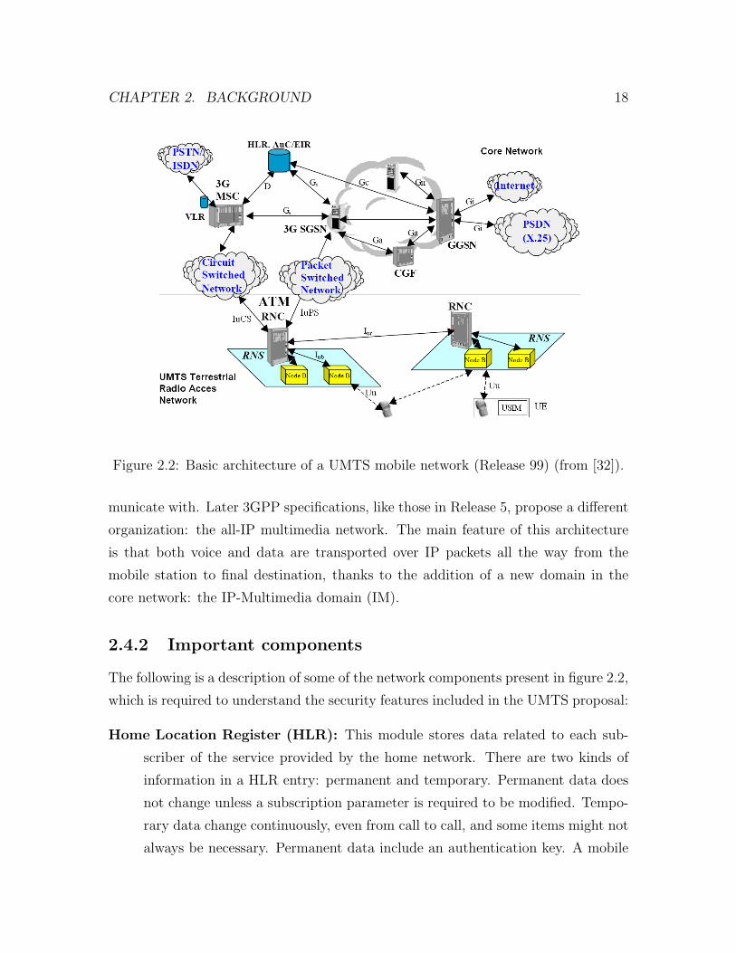
CHAPTER 2. BACKGROUND 18
Figure 2.2: Basic architecture of a UMTS mobile network (Release 99) (from [32]).
municate with. Later 3GPP specifications, like those in Release 5, propose a different
organization: the all-IP multimedia network. The main feature of this architecture
is that both voice and data are transported over IP packets all the way from the
mobile station to final destination, thanks to the addition of a new domain in the
core network: the IP-Multimedia domain (IM).
2.4.2 Important components
The following is a description of some of the network components present in figure 2.2,
which is required to understand the security features included in the UMTS proposal:
Home Location Register (HLR): This module stores data related to each sub-
scriber of the service provided by the home network. There are two kinds of
information in a HLR entry: permanent and temporary. Permanent data does
not change unless a subscription parameter is required to be modified. Tempo-
rary data change continuously, even from call to call, and some items might not
always be necessary. Permanent data include an authentication key. A mobile

CHAPTER 2. BACKGROUND 19
network can have several HLRs depending on the size of its coverage area.
Visitor Location Register (VLR): The VLR holds information related to every
mobile station that roams into the area serviced by the associated MSC. It
contains information about the active subscribers in the corresponding serving
network, even those to whom the network is not their home network. When
a subscriber roams into a serving network, the information in his/her HLR is
copied to the VLR in the visited network, and discarded when the subscriber
leaves such network. The information stored by the VLR is quite the same as
that stored by the HLR.
Authentication Center (AuC): Physically attached to a HLR, this component
stores, for each subscriber, an authentication key K and the corresponding
International Mobile Subscriber Identity (IMSI), which are permanent data
entered at subscription time. The AuC plays a crucial role in the network’s
security architecture, since it is responsible of the generation of important data
used during the authentication and encryption procedures.
Serving GPRS Support Node (SGSN): This component is responsible for the
mobility management and IP packet session management. It routes user packet
traffic from the radio access network to the appropriate Gateway GPRS Support
Node (GGSN), which in turn provides access to external packet data networks.
In addition, it generates records to be used by other modules for charging pur-
poses. SGSN helps to control access to network resources, preventing unau-
thorized access to the network or specific services and applications. The IuPS
interface links the SGSN, the main component of the PS domain, with the Radio
Network Controller (RNC) in the UTRAN, as figure 2.2 illustrates.
2.5 UMTS’ security architecture
According to the specifications, the security architecture is made up of a set of security
features and security mechanisms [2]. A security feature is a service capability that
meets one or several security requirements. A security mechanism is an element or

CHAPTER 2. BACKGROUND 20
process that is used to carry out a security feature. Figure 2.3 shows that the security
features are grouped together in five different sets of features, each one facing a specific
threat and accomplishing certain security objectives. The following is a description
of these groups of features:
Network access security (I): Provides secure access to 3G services and protects
against attacks on the radio interface link.
Network domain security (II): Allows nodes in the operator’s network to se-
curely exchange signaling data and protects against attacks on the wired net-
work.
User domain security (III): Secures access to mobile stations.
Application domain security (IV): Enables applications in the user and in the
provider domain to securely exchange messages.
Visibility and configurability of security (V): Allows the user to get informa-
tion about what security features are in operation or not, and whether provision
of a service depends on the activation of a security feature or not.
An exhaustive study of the literature revealed that some of the mechanisms that carry
out the set of network access security features require the execution of algorithmic
processes with the highest performance possible.
2.5.1 Network access security features
Network access security features can be further classified into the following categories:
entity authentication, confidentiality and data integrity. The following is a description
of the security features classified into the category of entity authentication:
User authentication: The Serving Network (SN in figure 2.3), the network that
provides the service to the user, corroborates the identity of the Mobile Equip-
ment (ME).

CHAPTER 2. BACKGROUND 21
Figure 2.3: Overview of the security architecture (from [2]).
Network authentication: The user corroborates that he/she is connecting to a
serving network that is authorized by the user’s Home Network (HE in figure
2.3) to provide him/her with the service; this includes the guarantee that this
authorization is recent.
The following security features deal with the confidentiality of data along the
network access link:
Cipher algorithm agreement: The mobile station and the serving network can
securely negotiate the algorithm that they shall use subsequently.
Cipher key agreement: The mobile equipment and the serving network agree on
a cipher key that they may use subsequently.
Confidentiality of user data: User data can not be overheard on the radio inter-
face.
Confidentiality of signaling data: Signaling data can not be overheard on the
radio interface.
The features provided to achieve integrity of data on the network access link are
the following:
CHAPTER 2. BACKGROUND 22
Integrity algorithm agreement: The mobile equipment and the serving network
can securely negotiate the integrity algorithm that they shall use subsequently.
Integrity key agreement: The mobile station and the serving network agree on an
integrity key that they may use subsequently.
Data integrity and origin authentication of signaling data: The receiving en-
tity (mobile station or serving network) is able to verify that signaling has not
been modified in an unauthorized way since it was transmitted by the send-
ing entity (serving network or mobile equipment) and that the origin of the
signaling data received is indeed the one claimed.
2.5.2 UMTS Authentication and Key Agreement
The UMTS Authentication and Key Agreement (UMTS AKA) is a security mech-
anism used to accomplish the authentication and key agreement features described
above. This mechanism is based on a challenge/response authentication protocol con-
ceived to be compatible with GSM’s subscriber authentication and key establishment
protocol to facilitate the transition from GSM to UMTS. A challenge/response pro-
tocol is a security measure in which an entity verifies the identity of another entity
without revealing a secret password shared by the two entities. The key concept is
that each entity must prove to the other that it knows the password without actually
revealing or transmitting such password.
The UMTS AKA process is invoked by a SN after a first registration of a user, after
a service request, after a location update request, after an attach request and after
a detach request or connection re-establishment request. In addition, the relevant
information about the user must be transferred from the user’s home network to the
serving network to complete the process. The home network’s HLR/AuC provides
the serving network’s VLR/SGSN with Authentication Vectors (AVs).
The authentication and key agreement process is summarized in the following
algorithm and illustrated in figure 2.4:
Stage 1:

CHAPTER 2. BACKGROUND 23
Figure 2.4: Authentication and key agreement security mechanism (from [2]).

CHAPTER 2. BACKGROUND 24
1. The visited network’s VLR/SGSN requests a set of AVs from the HLR/AuC in
the user’s home network.
2. The HLR/AuC computes an array of AVs. This is done by means of the au-
thentication algorithms and the user’s private secret key K, which is stored only
in the home network’s HLR/AuC and the USIM in the user’s mobile station.
3. The home network’s HLR/AuC responds by sending n authentication vectors
AV1, . . . , AVn back to the visited network’s VLR/SGSN.
Stage 2:
1. The visited network’s VLR/SGSN chooses one AV and challenges mobile sta-
tion’s USIM by sending the RAND and AUTN fields in the vector to it.
2. The mobile station’s USIM processes the AUTN. With the aid of the private
secret key K, the user is able to verify that the received challenge data could
only have been constructed by someone who had access to the same secret key
K. The USIM will also verify that the AV has not expired by checking its
sequence number (SEQ) field. Provided that the network can be authenticated
and that the AV is still valid, the USIM proceeds to generate a confidentiality
key (CK), an integrity key (IK) and a response for the network (RES).
3. The user equipment responds with RES to the visited network.
4. The visited network’s VLR/SGSN verifies that response is correct by comparing
the expected response (XRES) from the current AV with the response (RES)
received from the mobile station’s USIM.
2.5.3 Integrity
Since the control signaling information transmitted between the mobile station and
the network is so important and sensitive, its integrity must be protected. The
mechanism that carries out this security feature is based on an UMTS Integrity
Algorithm (UIA) implemented both in the mobile station and in the module of the
UTRAN closer to the core network, i.e. the RNC. See figure 2.2.

CHAPTER 2. BACKGROUND 25
Figure 2.5: Derivation of message authentication codes from signaling information
using the f9 algorithm (from [4]).
The UIA explained in this subsection is the f9 algorithm, shown in figure 2.5. The
procedure of signaling data integrity verification in the uplink direction consists of
four steps. First, the f9 algorithm in the user equipment computes a 32-bit message
authentication code for integrity of signaling data (MAC-I) based on its input pa-
rameters, including the signaling data (MESSAGE). Second, the MAC-I computed is
attached to the signaling information and sent over the radio interface from the user
equipment to the RNC. Third, the RNC computes an expected message authentica-
tion code value (XMAC-I) once it has received the signaling data and the MAC-I,
in the same way as the mobile station computed MAC-I. Fourth, the integrity of the
signaling information is determined by comparing the MAC-I and the XMAC-I. The
process of integrity verification in the downlink direction is the same.
Figure 2.6 shows that the internal structure of the f9 algorithm uses the shared
integrity key IK and it is based on a series of KASUMI block ciphering modules
interconnected in a variant of the Cipher Block Chaining (CBC) mode [16]. The
algorithm combines the 64-bit intermediate outputs of all of the block ciphers by
using XOR operations, and, lastly, applies the KASUMI algorithm to this sum. The
64-bit output of this final process is truncated to 32 bits to obtain the MAC-I value.
A thorough description of the parameters of the f9 algorithm is provided in [4]
and [33].

CHAPTER 2. BACKGROUND 26
Figure 2.6: The f9 integrity algorithm (from [4]).
2.5.4 Confidentiality
Unlike the integrity algorithm, which only operates on signaling information, the
confidentiality mechanism operates on both signaling information and user data. The
algorithm defined to perform the confidentiality tasks is called f8 .
The confidentiality process carried out by the f8 algorithm in the uplink direction
consists of five steps. First, using the ciphering key CK, and some other parameters,
the f8 algorithm in the user equipment computes an output keystream block. Second,
this output keystream block is XORed, bit by bit, with the data stream, also called
plaintext , to obtain a ciphered data block or ciphertext . Third, the ciphertext is sent
to the network through the radio interface. Fourth, the f8 algorithm in the RNC uses
the parameters employed by the user equipment, including the shared cipher key CK,
to generate the same output keystream that was computed in the user equipment.
Finally, this keystream is XORed with the ciphertext received to recover the initial
information. Figure 2.7 illustrates the procedure, which is the same for the downlink
case.
Figure 2.8 illustrates the structure of the f8 algorithm. Once again, notice that
several instances of the KASUMI block cipher are present, this time organized in a so

CHAPTER 2. BACKGROUND 27
Figure 2.7: Ciphering of user and signaling data using the f8 algorithm (from [4]).
called Output Feedback (OFB) mode [16]. Each block cipher generates 64 bits of the
whole output keystream and forwards its output to the input of the following block
cipher, subject to its modification by a XOR operation with a counter and a static
value.
The input parameter LENGTH indicates the length of both the keystream and
the plaintext stream. The parameter BEARER identifies to each radio bearer among
those associated with each user; this input value avoids the use of the same keystream
for encryption/decryption in every radio bearer. For more information refer to [4] and
[33].
2.5.5 The KASUMI block cipher
Not only was the KASUMI block cipher adopted by the 3GPP as the cornerstone of
the operations involved in the security architecture defined for the third generation
UMTS standard, but also of those in the security architectures for the evolved second
generation GSM standard, and the second generation + GPRS standard. Therefore,
KASUMI is the main primitive of the f8 confidentiality algorithm, the f9 integrity
algorithm, and the A5/3 and GEA3 encryption/decryption algorithms [8].
KASUMI’s specifications were developed based on previous work carried out for
MISTY [25], an algorithm that has proven its security against the most advanced
cryptanalysis techniques and is suitable for hardware implementation. KASUMI has

CHAPTER 2. BACKGROUND 28
Figure 2.8: The f8 confidentiality algorithm (from [4]).
a Feistel structure comprising eight rounds, operates on 64-bit data blocks, its pro-
cessing is controlled by a 128-bit encryption key K, and has the following additional
features derived from its Feistel nature [5]:
• Input plaintext is the input to the first round.
• Ciphertext is the last round’s output.
• K is used to generate a set of round keys {KLi, KOi, KIi} for each round i.
• Each round computes a different function as long as the input round keys are
different.
• The same algorithm is used both for encryption and decryption.
Figure 2.9 shows the structure and components of the KASUMI block cipher. For
odd rounds the round-function is computed by applying the FL function followed by
the FO function. For even rounds the FO function is applied before FL. FL, shown in
figure 2.9(d), is a 32-bit function made up of simple AND, OR, XOR and left rotation
operations. FO, see figure 2.9(b), is also a 32-bit function having a three-round Feistel
organization which contains one FI block per round. FI, see figure 2.9(c), is a non-
linear 16-bit function having itself a four-round Feistel structure; it is made up of two

CHAPTER 2. BACKGROUND 29
1 2 3 4 5 6 7 8
KL1 K1 ≪ 1 K2 ≪ 1 K3 ≪ 1 K4 ≪ 1 K5 ≪ 1 K6 ≪ 1 K7 ≪ 1 K8 ≪ 1
KL2 K3′ K4′ K5′ K6′ K7′ K8′ K1′ K2′
KO1 K2 ≪ 5 K3 ≪ 5 K4 ≪ 5 K5 ≪ 5 K6 ≪ 5 K7 ≪ 5 K8 ≪ 5 K1 ≪ 5
KO2 K6 ≪ 8 K7 ≪ 8 K8 ≪ 8 K1 ≪ 8 K2 ≪ 8 K3 ≪ 8 K4 ≪ 8 K5 ≪ 8
KO3 K7 ≪ 13 K8 ≪ 13 K1 ≪ 13 K2 ≪ 13 K3 ≪ 13 K4 ≪ 13 K5 ≪ 13 K6 ≪ 13
KI1 K5′ K6′ K7′ K8′ K1′ K2′ K3′ K4′
KI2 K4′ K5′ K6′ K7′ K8′ K1′ K2′ K3′
KI3 K8′ K1′ K2′ K3′ K4′ K5′ K6′ K7′
Table 2.1: Key scheduling for the KASUMI algorithm.
nine-bit substitution boxes (S-boxes), each called S9, and two seven-bit S-boxes, each
called S7. Figure 2.9(c) shows that data in the FI function flow along two different
paths: a nine-bit long path (thick lines) and a seven-bit path (thin lines). Notice
that in Feistel structures, such as the one used in this algorithm, each round’s output
is twisted before being applied as input to the following round. After completing
eight rounds KASUMI produces a 64-bit long ciphertext block corresponding to the
plaintext input block.
The key scheduler receives the 128-bit initial input key K and generates the round
keys KL (32-bit long), KO (48-bit long) and KI (48-bit long) for each of the eight
rounds. Each of these round keys is made up of two or three 16-bit subkeys, which
are the ones directly computed by the key scheduler in the fashion shown in table 2.1.
The diagrams in figure 2.9 illustrate how these subkeys are used within each of the
function modules within the rounds. The initial key K is also split into eight 16-bit
values Ki, 1 ≤ i ≤ 8.
In table 2.1 “≪” means a left rotation by the number of bits specified by the
number to the right, and each K ′i is defined as follows:
K ′i = Ki ⊕ Ci, 1 ≤ i ≤ 8;
where Ci is a constant specified in [5].

CHAPTER 2. BACKGROUND 30
KO1 KI1KL1
FOFL
KO2 KI2
FO
KL2
FL
KO3 KI3KL3
FOFL
KO4 KI4
FO
KL4
FL
64
3232
KO5 KI5KL5
FOFL
KO6 KI6
FO
KL6
FL
KO7 KI7KL7
FOFL
KO8 KI8
FO
KL8
FL
64
L0 R0
L8 R8
(a) Feistel
structure
KOi,1
KIi,1FIi1
KOi,2
KIi,2FIi2
KOi,3
KIi,3FIi3
32
32
1616
(b) FO block
9 7
S9
S9
S7
S7
16
16
KIij1
KIij2
(c) FI block
AND
OR
<<<1
<<<1
KLi1
KLi2
16 16
32
32
(d) FL block
Figure 2.9: The KASUMI block cipher.

CHAPTER 2. BACKGROUND 31
Figure 2.10: The KGCORE keystream generator function (from [8]).
2.6 Security issues for 2G and 2.5G networks
As mentioned previously, the 3GPP consortium currently has the responsibility of the
maintenance of the set of specifications for GSM and GPRS, including those for the
A5/3 and GEA3 stream ciphers. Both of these algorithms are built around a common
function module called KGCORE, which is based on the KASUMI block cipher.
2.6.1 The KGCORE function
The organization of the KGCORE, illustrated in figure 2.10, function is identical
to the organization of the f8 stream cipher. As in f8 , the KASUMI instances are
connected in an OFB mode, where the feedback data are modified by a static value
and a 64-bit counter.
KGCORE has seven input parameters (CA, CB, CC, CD, CE, CK and CL) with
variable lengths, and one output (CO). The A5/3 and GEA3 algorithms are defined
by appropriately mapping their inputs to the KGCORE module’s inputs, and KG-
CORE’s output to the algorithm’s outputs.

CHAPTER 2. BACKGROUND 32
Figure 2.11: The A5/3 stream cipher (from [8]).
2.6.2 The A5/3 algorithm for GSM
The A5/3 algorithm generates two 114-bits keystream blocks; one is employed for
the encryption and decryption processes in the uplink direction, and the other in for
encryption and decryption in the downlink direction. Figure 2.11 shows the input
and output parameters of the A5/3 algorithm and the information passed to the
KGCORE function block.
2.6.3 The GEA3 algorithm for GPRS
The GEA3 algorithm generates an M-byte keystream block, where M is variable that
never exceeds 216 = 65536. Figure 2.12 shows the input parameters of the GEA3
algorithm and their mapping to the inputs of the KGCORE function module. For
this algorithm, KGCORE’s CO output has a length, in bits, of eight times the value
of the integer M.
More information about KGCORE, A5/3 and GEA3 can be found in references
[8] and [33].

CHAPTER 2. BACKGROUND 33
Figure 2.12: The GEA3 stream cipher (from [8]).

Chapter 3
State of the art
This chapter describes the strategies proposed in the past to design hardware mod-
ules for the KASUMI block cipher and the f8 , f9 and GEA3 algorithms. The results
obtained after implementing those architectures in FPGA technology are provided
as well. This chapter includes a section that analyzes the advantages and disadvan-
tages of the previous proposals and deduces a set of requirements and useful design
strategies from the discussion. The last section of this chapter describes the Motorola
MPC185 security coprocessor, which includes a functional unit (FU) to perform the
f8 and f9 algorithms.
3.1 Implementation of the KASUMI block cipher
Several principles to implement a Feistel block cipher in hardware are described in
[14]. The first choice is to implement only a small number N of rounds and then
iterate over them, feeding back the output of the Nth round to the input of the first
round until the required number of rounds has been carried out. Improvements to
this technique include the addition of inner- and outer-round pipeline registers. The
second scheme consists of unrolling the whole number of rounds and adding inner-
and outer-round pipeline stages to the design. While the first strategy is aimed to
be used when area restrictions are strong, the second strategy is used to reach the
maximum throughput possible without space restrictions.
34

CHAPTER 3. STATE OF THE ART 35
(a) Type 1 (b) Type 2
Figure 3.1: Single-round architectures implementing the KASUMI block cipher (from
[20]).
The emphasis of this section is to show the different techniques to implement the
Feistel structure of the KASUMI block cipher and the key scheduler, as well as their
implementation results.
3.1.1 Iterative and reuse-based designs
The two architectures proposed by [20] implement logic for only one round, i.e. the
FO and the FL function blocks. The first architecture, called Type 1, iterates over
these two components eight times until completion of the process, feeding the design’s
output back to its input at the end of each iteration. It is a simple component that
sacrifices performance in the interests of achieving low hardware complexity, low
power consumption, and suitability for implementation in mobile stations. Figure
3.1(a) illustrates this proposal.
Figure 3.1(b) shows the second design, the Type 2 architecture, which is intended
to be implemented within the RNC in the UTRAN section of a UMTS network. High

CHAPTER 3. STATE OF THE ART 36
performance is needed to fulfill encryption/decryption requests from several users.
Therefore, this proposal contains a four-stage inner-round pipelined FO module that
results in an increased operating frequency and an improved throughput, by a factor
of four. Notice in figure 3.1(b) that the FL function is replicated twice to avoid
conflicts.
Both architectures were developed using the VHDL language, and implemented in
devices belonging to the Virtex-E family of FPGAs from Xilinx. Type 1 architecture
turns out to be such an inexpensive implementation in terms of hardware resources,
requiring 650 slices, when compared to Type 2 architecture, which requires 1100
slices. Concerning performance, Type 2 architecture has a throughput of 234 Mbps,
working at a clock frequency of 33 MHz, whereas Type 1 design has a throughput of
110 Mbps, synchronized with a clock working at 20 MHz.
The goal of the work documented in [24] is to investigate the suitability of the
KASUMI block cipher for hardware implementation. The two architectures proposed
are implemented in Xilinx Virtex-E and Altera APEX 20KE FPGA technologies, as
well as in Atmel’s 0.25 µm Application-Specific Integrated Circuit (ASIC) technology,
and highlight the principle that a trade-off between area and speed must be considered
when designing. The first proposal’s goal is to reduce the area required to implement
the block cipher by implementing a two-round iterative architecture, see figure 3.2.
An interesting fact about this design is that the S7 and S9 S-boxes are implemented
as combinational logic and, alternatively, mapped to embedded memory blocks within
the FPGA, taking advantage of Xilinx’s Block SelectRAM+ (BRAM) and Altera’s
Embedded System Block (ESB) technologies. This design requires 24 BRAM blocks
when implemented in Virtex-E FPGAs, 12 blocks for each round, and 48 ESB blocks
for devices from Altera, 24 blocks for each round.
The registers at the end of each round make the architecture to have a total com-
pletion latency of 8 clock cycles when the S-boxes are implemented as combinational
modules, and 40 cycles when the S-boxes are mapped to embedded memory blocks;
this due to the inner-round pipeline stages introduced by the registered outputs of
the synchronous memory blocks. However, this two-round design is not intended to
work in a pipelined fashion, i.e. ciphering two blocks during each clock cycle, though.

CHAPTER 3. STATE OF THE ART 37
Figure 3.2: Two-round iterative KASUMI architecture (from [24]).
Clock Frequency Throughput
Technology Architecture (MHz) (Mbps) Area
Xilinx two-round comb. 20.88 167.04 1287 slices
two-round BRAM 35.35 70.70 749 slices
Altera two-round comb. 31.17 249.36 2077 logic elements
two-round ESB 61.30 122.60 821 logic elements
ASIC two-round comb. 90.421 723.37 N/A
Table 3.1: Implementation results for the two-round architecture.
Table 3.1 reports the results obtained after performing the implementation process
of the two versions of the two-round design on the three platforms. Notice that the
process for Altera devices produces architectures with higher clock frequencies and
throughputs. The number of slices required by the Virtex-E devices is less than the
number of logic elements for the APEX devices. However, this is not conclusive
since the organization of Xilinx’s FPGAs differs from the organization of the Altera’s
FPGAs. The ASIC implementation has the highest throughput and clock frequency
even when the S-boxes are implemented using combinational logic.
It is possible to manipulate the structure of the KASUMI block cipher, by means
of aggressive simplifications, to get inexpensive datapaths with long latencies that
carry out the ciphering process. The work reported in [29] presents the application
of a simplification technique to design two KASUMI architectures requiring less than
600 slices in Virtex-E FPGAs and having latencies of 56 and 32 cycles, respectively.

CHAPTER 3. STATE OF THE ART 38
Latency Clock Frequency Throughput Area
Proposal (Cycles) (MHz) (Mbps) (Slices)
1 56 68.13 77.86 368
2 32 58.06 116.12 370
3 8 33.14 265.12 588
Table 3.2: Implementation results for the simplified architectures.
A third architecture with a latency of eight cycles is mentioned, and its results pro-
vided, but not described. Figure 3.3 shows the datapaths obtained after applying the
simplification strategy proposed by the authors.
Table 3.2 shows the results obtained after implementing the three architectures
in a Virtex-E FPGA. These designs are cheaper in terms of hardware resources than
the former two proposals. Notice that the first architecture, the cheapest one, has
the higher clock frequency and the lowest throughput. This situation is explained by
the following expression:
throughput =block size× clock frequency
latency. (3.1)
For the three architectures the size of the block is fixed, 64 bits, whereas the clock
frequency and the latency values change for every design. The expression (3.1) indi-
cates that as the latency increases, the throughput decreases in such a way that the
performance is affected.
The two-round architecture described in [21], and shown in figure 3.4, is similar
to that described in [24]. However, the proposal takes advantage of both inner- and
outer-round pipeline techniques to decrease the period of the clock and increase the
throughput. Inner-round registers are negative edge-triggered, whereas outer-round
registers are positive edge-triggered; consequently, the execution time of each round
is one clock cycle. The pipelined design allows this circuit to process two blocks
simultaneously, with an initial latency of eight cycles. The S-boxes in this architecture
are implemented with combinational logic.
The implementation results of this architecture, in a Virtex-E platform, are the
following: 1726 Configurable Logic Blocks (CLBs), which is equivalent to 3452 slices,
a clock frequency of 54 MHz and a throughput of 432 Mbps.

CHAPTER 3. STATE OF THE ART 39
(a) 56-cycle architecture (b) 32-cycle architecture
Figure 3.3: Two simplified iterative KASUMI architectures (from [29]).

CHAPTER 3. STATE OF THE ART 40
Figure 3.4: Two-round dual edge-triggered pipelined KASUMI architecture (from
[21]).
3.1.2 Pipelined designs
The second architecture proposed in [24] is shown in figure 3.5, its goal is to maximize
throughput by implementing an unrolled eight-round outer-round pipelined datapath.
This design requires four times more hardware resources than the two-round design in
figure 3.2. There are also two variants of this architecture: the first variant includes
combinational S-boxes, whereas the second one implements S-boxes using embedded
memory blocks. In the first case, the initial latency is 9 clock cycles, and in the second
case the initial latency is 41 cycles. A new plaintext block enters the datapath every
clock cycle and, once the pipeline fills, the datapath issues a ciphertext block each
clock cycle.
The results of the implementation process for this design are shown in table 3.3.
Again, the FPGA implementations in the Altera devices achieve the highest through-
puts and clock frequencies. The following expression to compute throughput in a
pipelined architecture illustrates why these designs achieve performance above 1 Gbps:
throughput = block size× clock frequency. (3.2)
Figure 3.6 illustrates the eight-round architecture described in [21]. This datapath,

CHAPTER 3. STATE OF THE ART 41
Figure 3.5: Eight-round pipelined KASUMI architecture (from [24]).
Clock Frequency Throughput
Technology Architecture (MHz) (Mbps) Area
Xilinx eight-round comb. 20.86 1335.04 4032 slices
eight-round BRAM 37.72 2414.08 2213 slices
Altera eight-round comb. 26.24 1994.88 7106 logic elements
eight-round ESB 40.50 3221.12 2316 logic elements
ASIC eight-round comb. 94.05 5786.94 N/A
Table 3.3: Implementation results for the eight-round architecture.

CHAPTER 3. STATE OF THE ART 42
Figure 3.6: Eight-round dual edge-triggered pipelined KASUMI architecture (from
[21]).
like the one shown in figure 3.4, contains an inner- and an outer-round pipeline; the
outer-round registers trigger during the positive edge of the clock signal, and the
inner-round registers trigger during the negative edge. Unlike the pipelined datapath
described previously, the initial latency of this circuit is only eight clock cycles due
to its dual edge-triggered design and the implementation of combinational S-boxes.
The implementation results of this architecture for a Virtex-E FPGA platform
are the following: a total number of 4738 CLBs required, equivalent to 9476 slices, a
clock frequency of 56 MHz and a throughput of 3584 Mbps.
3.1.3 KASUMI soft core
The company sci-worx commercializes an intellectual property (IP) core, available
in VHDL and Verilog HDL, implementing the KASUMI block cipher as part of its

CHAPTER 3. STATE OF THE ART 43
Figure 3.7: KASUMI intellectual property core from sciworx (from [30]).
DesignObjectsTM line of reusable cores ready to synthesize. Figure 3.7 shows the
design of the core.
The core’s top level component is called kasumi do and contains three functional
units implementing an odd round, and even round and the key scheduling, respec-
tively. The core receives the ciphering keys and the plaintext blocks through its input
ports and is controlled by some input signals. The core is fully synchronous and
takes one clock cycle to perform one round; thus, it needs eight cycles to complete
the ciphering task.
Implementation data indicate that the core needs 1150 slices and reaches a clock
frequency of 25 MHz in a Xilinx Virtex 1000 FPGA, no information concerning
throughput is provided.
3.2 Implementations of the key scheduler
This section presents the strategies employed by the designers of the previously de-
scribed KASUMI architectures to implement the block cipher’s key scheduler. Unfor-

CHAPTER 3. STATE OF THE ART 44
Figure 3.8: Key scheduler for the single-round pipelined architecture (from [20]).
tunately, not all of the references contain thorough descriptions of the architectures
proposed.
The key scheduler corresponding to the KASUMI architecture in figure 3.1(b)
stores four ciphering keys in its 32 16-bit registers, see figure 3.8. The control rotates
the array of registers and the scheduler computes the subkeys needed for each pipeline
stage during each cycle. The ciphering process for the first block concludes after
rotating the array 32 times. Successive rotations will allow the next blocks to reach
the final stage of the ciphering process. It may be that new ciphering keys are stored
in the array of registers, if necessary, after an already stored key has been rotated
throughout the array.
The key scheduler proposed in [29] for the architectures in figure 3.3, and illus-
trated in figure 3.9, is also a shift register architecture, where the initial key is rotated

CHAPTER 3. STATE OF THE ART 45
Figure 3.9: Key scheduler for simplified architectures (from [29]).
to the left during encryption and to the right during decryption. The Kin 16-bit input
port is used to load the 128-bit initial key into the scheduler’s registers after eight
clock cycles, the barrel shifter stores the constants to be used during computation of
the subkeys and the logic modules generate the subkeys. The registers are shifted
every cycle for the 1 cycle/round architecture; and every 7 and 4 cycles for the 7
cycles/round and 4 cycles/round architectures, respectively.
The key scheduler presented in [21], and illustrated in figure 3.10, computes a
number of 16-bit subkeys by means of an array of left rotation modules and a set of
XOR gates. By concatenating some of these 40 subkeys the scheduler generates the
round keys for the Feistel implementations in figures 3.4 and 3.6. These round keys
are stored in a register file to accelerate the ciphering process.
3.3 Implementations of the f8 and f9 algorithms
The hardware implementations of f8 and f9 proposed in [24] consider that the algo-
rithms will work with data whose length ranges between 1 and 5114 bits. Processing
pieces of data with such lengths implies that a hardware module implementing the f8
algorithm contains from 1 up to 80 instances of any of the KASUMI designs described
in the previous section, which is costly. Figure 3.11 illustrates that the architectures
designed implement the algorithms by iterating, at most 80 times, over a single KA-

CHAPTER 3. STATE OF THE ART 46
Figure 3.10: Key scheduler for dual edge-triggered KASUMI architectures (from [21]).
SUMI module; generating a 64-bit block of the keystream, in the case of f8 , and an
operand for the XOR-sum required to compute the MAC-I value, in the case of f9 ,
during each iteration. Another KASUMI module is required in f8 prior the iteration
to set the register A properly. In f9 , the second KASUMI module is placed after the
iteration to compute the MAC-I value based on the result of the iteration phase.
Table 3.4 shows the results obtained after implementing the design for f8 in the two
FPGA platforms. The architecture uses the two variants of the two-round KASUMI
core (figure 3.2) and one variant of the eight-round datapath (figure 3.5), the one
implementing combinational S-boxes. There are not enough memory blocks to store
the 192 S-boxes required by the two KASUMI modules included in the designs.
The throughput for the architecture using the two-round variant using combina-
tional S-boxes is computed by:
throughput =block size× number of blocks× clock frequency
(number of blocks + 1)× 8. (3.3)
For the architecture using memory blocks for the S-boxes, the throughput is given
by:
throughput =block size× number of blocks× clock frequency
(number of blocks + 1)× 40. (3.4)

CHAPTER 3. STATE OF THE ART 47
(a) f8 (b) f9
Figure 3.11: Iterative architectures implementing f8 and f9 (from [24]).
In both cases remember that block size = 64 and 1 ≤ number of blocks ≤ 80.
Table 3.5 shows implementation data for the f9 architecture. This time, the
performance metric is the time required to generate a message authentication code
from a variable-length message. The expression to compute this parameter is as
follows:
time =(number of blocks + 1)× latency
clock frequency. (3.5)
Remember that latency is the number of clock cycles needed by the KASUMI module
Clock Frequency
Technology Architecture (MHz) Area
Xilinx two-round comb. 20.52 2781 slices
two-round BRAM 33.14 1563 slices
eight-round comb. 20.01 8146 slices
Altera two-round comb. 30.76 4687 logic elements
two-round BRAM 49.50 2128 logic elements
eight-round comb. 29.06 15232 logic elements
Table 3.4: Implementation results for the f8 architecture.

CHAPTER 3. STATE OF THE ART 48
Clock Frequency
Technology Architecture (MHz) Area
Xilinx two-round comb. 20.68 2671 slices
two-round BRAM 33.52 1560 slices
eight-round comb. 20.19 8104 slices
Altera two-round comb. 29.62 4382 logic elements
two-round BRAM 51.79 1901 logic elements
eight-round comb. 28.93 13628 logic elements
Table 3.5: Implementation results for the f9 architecture.
Figure 3.12: Merged architecture for f8 and f9 (from [29]).
to carry out the ciphering process on a 64-bit block. As before
1 ≤ number of blocks ≤ 80.
The design proposed in [29] also considers input data and messages with a length
of at most 5114 bits; its most remarkable feature is that it carries out both the f8 and
f9 algorithms with the same architecture, see figure 3.12. Special care was taken to
not add expensive and unnecessary components to the design, as well as implementing
the combination of the ciphering and integrity keys with the key modifiers (KMs) in
an efficient manner.
Table 3.6 shows the implementation results for this architecture. The first set of
data were obtained after synthesizing to a Virtex-E device using a speed grade of −8,

CHAPTER 3. STATE OF THE ART 49
Latency Area Frequency Throughput
Speed grade (cycles) (slices) (MHz) (Mbps)
-8 56 511 59.88 68.43
32 544 51.96 103.92
8 741 30.12 240.96
-6 56 512 51.15 58.46
32 544 44.42 88.84
8 742 25.80 206.40
Table 3.6: Implementation results for the merged architecture.
whereas the second data set corresponds to an implementation on a device with a
speed grade of −6.
3.4 Analysis of the implementations of the KA-
SUMI block cipher
The UMTS’ requirements specification for cryptographic algorithms [3] states that
hardware designs of the confidentiality and integrity algorithms should be imple-
mented using less than 10000 gates, achieve throughputs of at least 2 Mbps both
on the downlink and the uplink direction, and work using clock frequencies upwards
20 MHz. In addition, these hardware modules must be allocated both to the user
equipment and the RNC.
Even though each of the architectures for f8 and f9 described in the previous
section fulfills the requirements of throughput and clock frequency stated in [3], there
is still room for improvement in their designs. The following analysis emphasizes
the strengths and weaknesses of the proposals to implement the KASUMI algorithm,
since that module concentrates the most demanding processing.
The most advantageous feature of the Type 2 architecture described in [20], and
shown in figure 3.1, is that its pipelined datapath is able to process up to four plaintext
blocks at a time. However, in spite of this important characteristic, the complexity of
the FO function module does not allow the design to have a short critical path. The
only strategy considered to reduce the critical path is to insert an inner-round pipeline
register between the FI blocks, which is not enough since each FI module contains four

CHAPTER 3. STATE OF THE ART 50
S-boxes, presumably implemented with combinational elements, which prevent the
critical path from decreasing under a certain limit. The Type 1 architecture’s critical
path is even longer because this design contains the same number of components as
Type 2 architecture but does not contain inner-round pipeline registers. Implementing
any of these architectures as a functional unit inside a processor core will increase its
clock frequency and degrade its performance.
A very important lesson taught by the experiences reported in [24], see figures 3.2
and 3.5, is that mapping the S-boxes to embedded memory blocks produces higher
clock frequencies and has a significant effect on throughput. Although the results re-
ported for these proposals contain some inaccuracies concerning the number of mem-
ory blocks employed, the throughputs achieved by employing this mapping strategy
are rather good. The eight-round architecture is very expensive to be added as a
functional unit inside a processor core, it consumes lots of hardware resources and
embedded memory blocks. The two-round architecture would be a better choice, but
it can be improved further by performing some simplifications in the structure of the
rounds with the goal of saving resources and shortening the critical path.
Consuming too many hardware resources is a serious hindrance to incorporate an
architecture into a processor core; but it is not the only one. Having inexpensive
implementations of the integrity and confidentiality algorithms that have long laten-
cies is also a counterproductive situation because it degrades performance, no matter
the higher clock frequency, as revealed by the expression (3.1). This is the case of
the architectures proposed in [29] and shown in figure 3.3, which require many clock
cycles to encrypt one plaintext block and have long critical paths since there is no
any intermediate clock-driven device. Although the proposals are wisely designed and
fulfill the goal of being compact, it is possible to achieve a better tradeoff between
compactness and low latency by manipulating the structure of the KASUMI block
cipher in a different way to the proposed for these architectures.
Let us now examine the architectures described in [21], see figures 3.4 and 3.6.
Notice that not only do they have outstanding performances, as a consequence of
higher clock frequencies and shorter latencies in expressions (3.1) and (3.2), but are
among the most expensive designs. The key for the high frequencies is the use of

CHAPTER 3. STATE OF THE ART 51
negative edge-triggered inner-round registers and positive edge-triggered outer-round
registers, which is a smart way to reduce the critical path and constitutes the main
contribution of these works. The disadvantages of these proposals are that the S-boxes
are implemented as combinational logic and the Feistel structure is not simplified to
optimize the use of resources and decrease the critical path even further.
The previous discussion shows up the need for a KASUMI implementation that
meets the following requirements in order to be incorporated into a processor core:
• Its critical path must be shorter than the processor’s critical path in order for
its clock frequency does not affect the processor’s frequency.
• It must minimize the use of hardware resources by sharing modules.
• It must achieve a better tradeoff between performance and area complexity than
the proposals discussed previously.
The analysis also revealed the following useful strategies that are worth to be taken
into consideration when designing an architecture that meets the requirements:
• To transform the structure of the KASUMI block cipher without altering its
functionality so that the new structure has the following features: shared use
of resources, a shorter critical path and the possibility of reuse of a minimal
number of components.
• The implementation of the S-boxes using lookup table structures in hardware.
When using FPGAs, the embedded memory blocks are the most efficient al-
ternative to use this strategy. This technique is advantageous because it saves
hardware resources and, when the outputs of the memory modules are regis-
tered, contributes to reducing the critical path.
• The use of inner- and outer-round pipelines using both positive edge-triggered
registers and negative edge-triggered registers allows decreasing the design’s
critical path.

CHAPTER 3. STATE OF THE ART 52
Figure 3.13: Security system for GPRS mobile stations (from [22]).
3.5 Implementation of the GEA3 algorithm
The security system for GPRS mobile stations proposed in [22] includes hardware
implementations of the A3 and A8 algorithms [7], used to perform authentication
and ciphering key generation tasks, and the GEA3 keystream generator. The A3/A8
pair is intended to be included in the SIM smart card, whereas the GEA3 module lies
within the mobile equipment. Figure 3.13 shows the organization of the system.
The GEA3 module, see figure 3.14, is able to encrypt and decrypt data whose
length varies between 1 and M bytes, where 1 ≤ M ≤ 65536; it is controlled by a
128-bit ciphering key K ′c = Kc||Kc, where Kc is the encryption key generated by the
A8 algorithm; and it works by iterating over the KASUMI pipelined implementation
in figure 3.4, but with the restriction that the ciphering processing for a new block
is started after completion of the former one. This architecture is actually an imple-
mentation of the KGCORE function, which is identical to the f8 algorithm. Notice
the similarities between this design and that in figure 3.12.
The results of the implementation process, carried out in a Virtex-E platform, for
this design are the following: 2687 CLBs, equivalent to 5374 slices, and a clock fre-
quency of 33 MHz. A throughput of 363 Mbps is reported, but there is no information

CHAPTER 3. STATE OF THE ART 53
Figure 3.14: Iterative GEA3 architecture (from [22]).
concerning the number of iterations required to reach that throughput.
3.6 The MPC185 security coprocessor
Previous sections describe different published proposals that implement cryptographic
functions for UMTS networks in hardware, with different levels of performance and
hardware utilization. But, what commercial security solutions exist for the telecom-
munications market? what strategies do these technologies use to provide 3G cellular
networks with efficient security services? This section describes the Motorola MPC185
security coprocessor [27], which contains execution units intended to accelerate dif-
ferent cryptographic operations, including the f8 and f9 algorithms.
3.6.1 Description of the coprocessor
There exist several cryptographic coprocessors manufactured by Motorola implement-
ing different algorithms and working with different bus technologies. The MPC190
and MPC184 devices include bus interfaces compliant with the PCI 2.2 standard, as
well as FUs to perform several functions. The MPC185 is designed to work within a

CHAPTER 3. STATE OF THE ART 54
Figure 3.15: Organization of the MPC185 security coprocessor (from [27]).
system based on the 60x bus and, unlike the devices mentioned before, includes an
execution unit implementing the KASUMI block cipher and the f8 and f9 algorithms.
Other operations provided by this coprocessor include elliptic curve arithmetic, gen-
eration of random numbers and the following algorithms: DES, 3DES, RC-4, SHA-1
and AES.
Figure 3.15 shows the organization of the coprocessor, which resides in the mem-
ory map of the system’s main processor. The MPC185’s 60x Interface employs mas-
ter/slave protocols to transfer 64-bit words between the bus and the device’s internal
modules, managing the communication between execution units and other devices
present in the bus in an independent of existing processor fashion. When program-
ming the MPC185, the user writes a bundle of information, known as data packet
descriptor , to one of the four crypto-channels within the coprocessor using the sys-
tem’s bus. The crypto-channel decodes the descriptor, books an execution unit, uses
the bus interface to fetch all the required data, sends information back to the bus
after the cryptographic operation completes, resets the execution unit, and notifies
when the processing over the descriptor is done. The control unit schedules the re-
quired activities and manages the on-chip resources, including the execution units
and their first-in first-out (FIFO) buffers, the bus interface and the internal busses
interconnecting the various components.
Data packet descriptors allow access the cryptographic functions of the coproces-
CHAPTER 3. STATE OF THE ART 55
sor, some of which are conceived to be multifunction to facilitate the implementation
of security protocols. The header of the descriptor indicates the service required and
specifies which FU to use and in which operation mode. This FU might require
fetching information from system memory to carry out its task. For this purpose,
the descriptor contains seven (length, pointer) pairs indicating the initial address of
the piece of data required and its length. The last component of the descriptor is a
pointer to the next descriptor to process.
The modes in which the control unit can configure the on-chip resources are the
following:
Host-controlled mode. An external host is directly responsible for all data move-
ment into and out of the resource. This bypasses the crypto-channels and the
control arbitration unit.
Static mode. The user can reserve a specific execution unit to a specific crypto-
channel. This removes the execution unit from control unit arbitration.
Dynamic mode. A crypto-channel can request a particular service from the cor-
responding available execution unit. The control unit is responsible for the
execution unit and the bus arbitration and management.
3.6.2 The KASUMI execution unit
The KASUMI execution unit within the MPC185 coprocessor (KEU) is able to carry
out either a single f8 operation or a f8 followed by a f9 operation or a single f9
operation or both of them simultaneously, depending on the operation mode the unit
is working on. The length of the block of data to process is between 1 and 5114 bits.
A key size register indicates the length, in bytes, of the ciphering key; its permitted
values are 16, when the KEU performs only one operation, and 32, in case the unit
simultaneously carries out the two algorithms.
During the processing of the f8 function, the KEU reads data from its input FIFO,
XORs these data with the keystream it computes, and places the results in the output
FIFO buffer. When carrying out the f9 function, the KEU reads the input message
from the input FIFO and stores the resulting MAC-I value in the unit’s Data Out

CHAPTER 3. STATE OF THE ART 56
register. Data are read from the input FIFO buffer 64 bits at a time. In a similar
manner, reading from the FIFO address space will pop 64 bits of message data from
the output FIFO.
The parameter values for the f8 and f9 functions, COUNT, BEARER and FRESH,
are written in registers whose addresses in the map are: 1410016, 1410816 and 1411016,
respectively. These registers make up the initialization vector (IV) of the KEU.
There is no further information which provides details of how the KASUMI block
cipher is designed and how the function algorithms are implemented.

Chapter 4
Problem statement
As stated in chapter 1, this dissertation tackles the problem of implementing UMTS’
security operations in an efficient way. The previous chapter described different iso-
lated hardware implementations of KASUMI, f8 and f9 that turn out not to be well-
suited to work within a larger processing equipment present in a UMTS network.
Thus, the efficiency also involves a non-intrusive coexistence with other modules in
the system that perform the rest of the operations required.
There are two general methods to solve the problem. The first alternative con-
sists of programming the functions as software modules for standard general purpose
processors or digital signal processors. In the second approach a central processing
element entrusts the computation of the security functions to a specialized coproces-
sor attached to the system bus, like the MPC185 security processor. The following
sections discuss these two approaches in depth.
4.1 The software approach
Programs compiled from a high-level language or an assembly language use exclusively
the instruction set specified by the architecture of a general purpose microprocessor.
Implementing the f8 and f9 entirely in software has the following drawbacks:
• The overhead introduced by the pipeline stalls occurred during the execution of
the large number of instructions making up each program reduces performance.
57

CHAPTER 4. PROBLEM STATEMENT 58
• Generally, the width of an embedded processor’s internal registers (32 bits)
is shorter than the width of the block to process (64 bits). Therefore, two
separate sequences of instructions are needed to process each 32-bit half of the
block. On the contrary, when processing either 16-bit or 9-bit or 7-bit long
data the program wastes the processor’s registers and its capabilities. Both
disadvantages may be solved by using a processor with a Single Instruction
Multiple Data (SIMD) instruction set.
• The program needs the processor to execute many of its bitwise logic instruc-
tions to implement each S-box. On the other hand, implementing the S-boxes as
lookup tables stored in the system’s memory requires several accesses to mem-
ory and bus requests, unless advanced caching strategies are employed. In any
case the overhead caused by the memory latencies and the cache management
has a negative effect on performance.
4.2 The coprocessor approach
The coprocessor unit that carries out the confidentiality and integrity operations is
attached to the system’s bus and communicates with the main processor and the
memory using data and control signals. There are two alternatives to design the
coprocessor unit: as an ASIC like the MPC185 coprocessor or as a hardware module
implemented in a FPGA-based development board.
The main advantage of the coprocessor scheme is that it frees the processor from
performing long sequences of instructions to accomplish the security functions, allow-
ing it to devote its resources to other tasks. In spite of this situation, the performance
of the systems implementing this approach is severely limited by the long latencies
introduced by the communication through the system bus. This bus might be the 60x
bus for the case of the MPC185 coprocessor or the PCI bus for a FPGA development
board attached, for instance, to a personal computer. In addition, unfulfilled bus
operations increase the delays even further.
The following is a description of the steps that the MPC185 coprocessor carries
out to read data from the 60x bus when working as a bus initiator, i.e. it is able to

CHAPTER 4. PROBLEM STATEMENT 59
issue read and write commands to other components through the bus [27]:
1. A crypto channel asserts its 60x request to the control unit.
2. The crypto channel issues an address and the length of the transfer.
3. The control unit acknowledges request to the crypto channel.
4. The control unit asserts request to the 60x interface module.
5. The control unit waits for 60x read to begin.
6. When 60x read begins, the control unit receives data from the 60x interface
module and performs a master write to the appropriate internal address using
the address supplied by the crypto channel.
7. Transfer continues until the 60x read is completed and the controller has written
all data to the appropriate internal address. The 60x interface module will
continue making 60x bus requests until the full data length has been read.
The former sequence shows up the number of delays the MPC185 may incur when
reading data from the bus, which might be either ciphertext blocks or keys. In
particular, notice the cycles spent on waiting for the bus interface unit to start the
reading procedure in step 5. Similarly, steps 6 and 7 indicate that several cycles might
be needed to fetch data from the bus. This high consumption of cycles considerably
degrades the overall system’s ciphering throughput. Hence the need for a scheme that
tightly couples the ciphering module with a processing datapath that carries out the
rest of the computational processing.
4.3 Solution proposal
The limitations of the pure software and coprocessor approaches to implement the se-
curity functions highlight the need for experimentation on a different design strategy.
This scheme consists on adding a functional unit to a general purpose processor core
that carries out the most computationally expensive operation within the security

CHAPTER 4. PROBLEM STATEMENT 60
functions, namely the KASUMI algorithm; extending the ISA with instructions that
have access to the new hardware; and coding the f8 and f9 functions as sequences
of the added instructions. By executing these software modules the processor would
employ fewer clock cycles for completion of the security functions than with other soft-
ware implementations, made up of only the processor’s integer and logic instructions.
In addition, there would be no need to access the system bus.
There is no any previous reference to an implementation of an integration approach
using the KASUMI algorithm in the revised literature, so this dissertation proposes
a novel method to solve the problem considered. The crucial problem of designing an
efficient functional unit implementing the KASUMI block cipher is solved first.
The hypothesis that the incorporation of a KASUMI functional unit into a gen-
eral purpose processor core is feasible is supported by the results of similar successful
works. The work in [15] concerns the acceleration of the Data Encryption Stan-
dard (DES) algorithm by means of an extension to the customizable ARCtangent
microprocessor. The work reported in [17] deals with a methodology to evaluate the
impact of extensions to an instruction set architecture both on software performance
and hardware efficiency. It provides important hints concerning the derivation of an
Application-Specific Instruction Set Processor (ASIP) from an extendible processor
core.

Chapter 5
Novel proposals to implement
KASUMI
This chapter describes the hardware architectures for the KASUMI algorithm de-
signed with the goal of meeting the requirements described in a previous chapter: a
short critical path, the use of shared resources and a good tradeoff between perfor-
mance and number of hardware components utilized. The first, second and fourth
architectures are iterative proposals based on the reuse of hardware components,
whereas the third architecture is a fully pipelined design.
The four architectures are designed in VHDL and the corresponding prototypes
implemented using FPGA technology. Among the virtues of FPGAs are: high flexibil-
ity, similar to that for software solutions; performance close to ASIC implementations;
fast prototyping and the possibility to experiment with reconfigurable solutions.
5.1 Reuse-based designs
The simplification techniques presented in this section are novel and allow the archi-
tectures to meet the requirements of sharing resources and achieving a good balance
between high performance and low area complexity.
61

CHAPTER 5. NOVEL PROPOSALS TO IMPLEMENT KASUMI 62
5.1.1 Reuse-based architecture 1
The main principle to design for reuse is to specify an architecture consisting of some
of the components that are needed to perform a round. This design is used every
clock cycle in such a way that the output at the end of one cycle is the input for
the next cycle. The fewer the components, the larger the number of cycles needed to
carry out the ciphering process for one block. Also, the fewer cycles the architecture
requires to perform the process, the more complex the architecture is in terms of area.
5.1.1.1 Datapath for the FO function
Instead of simplifying the algorithm at a lower level, for instance at the FI level as
in [29], the manipulation is carried out at a higher level, at the FO function level.
Figure 5.1 presents the process followed to design a datapath that reuses components
within FO. Figure 5.1(a) illustrates an alternative parallel view of the FO function
shown in figure 2.9.
• In 5.1(b) two XOR gates are added to FO to make the upper and lower sections
more similar without modifying the behavior of the function. If these two parts
were structurally the same, it would be possible to reduce the architecture to
only one section that carried out the whole FO function after two cycles.
• The lower section in figure 5.1(b) needs a right FI function block to be struc-
turally identical to the upper section in this modified FO block. In figure 5.1(c)
an additional FI block is added to the lower section. The multiplexers in each
section allow selecting the appropriate data flow.
• The whole datapath in figure 5.1(c) is now ready to be simplified. Figure 5.1(d)
shows the final design, which takes two cycles to complete the FO function.
Notice that multiplexers are necessary to supply the correct values both to the
XOR gates and the FI module depending on if the datapath is in the first or
second cycle.
Also notice that the datapath in figure 5.1(d) contains one dual input FI block,
called dpFI, instead of two FI blocks as in the previous diagrams. This situation is

CHAPTER 5. NOVEL PROPOSALS TO IMPLEMENT KASUMI 63
explained in more detail later because it constitutes another special feature of the
designs proposed in this document.
The control for this module is implemented as a finite state machine that sets the
multiplexers’ selector input properly each cycle. Since the design takes two cycles to
complete its processing, it requires a two-state control.
5.1.1.2 Datapath for the FI function
Figure 5.1(c) shows that the FO module requires two FI blocks to work properly. Since
FI contains two seven-bit S-boxes and two nine-bit S-boxes, the simplified datapath
that takes two cycles to complete the FO function requires a total number of eight
S-boxes. Implementing S-boxes using four 128×7 ROMs and four 512×9 ROMs is a
rather expensive choice in terms of area. The solution proposed is to map the S-boxes
to dual-port ROMs, which decreases by two the number of ROMs required. The use
of this technique exploits the principle of reuse even further because the same S-box
is now able to meet two requests at the same time.
Consider two instances of the FI block shown in figure 2.9(c), replace each pair
of S9 S-boxes located in the same position in the FI blocks by a single dual-port
S9 S-box and repeat this procedure with the pairs of S7 S-boxes. The result is the
datapath illustrated in figure 5.2, which only contains two dual-port S9 S-boxes and
two dual-port S7 S-boxes and combines two FI function blocks into one.
There are several notes to point out concerning this design. First, during the
implementation phase the four dual-port S-boxes are mapped to dual-port embedded
memory blocks inside the FPGA. Second, the embedded memory blocks are syn-
chronous and this dual-port FI datapath is required to provide its results after one
clock cycle; therefore, the upper S-boxes are designed to be negative edge-triggered,
whereas the lower S-boxes are designed to be positive edge-triggered, as indicated in
figure 5.2. Third, the registers shown in the figure, colored in grey, synchronize input
data with the values provided by the upper and lower S-boxes.
Notice that the datapath in figure 5.1(d) also has positive edge-triggered registers
used to synchronize input data used by logic that is located further on the dual-
port FI module in the datapath. Actually, every input signal that is to be used

CHAPTER 5. NOVEL PROPOSALS TO IMPLEMENT KASUMI 64
FI2FI1
FI3
KO1 KO2
KI1
KO3
KI3
KI2
32
32
16 16
16 16
Upper section
Lower section
(a) Step 1
FI1
KO1
KI1
16 16
FI2
KO2
KI2
FI3
KO3
KI3
32
16 16
32
0
0
(b) Step 2
FI1
KO1
KI1
16 16
FI2
KO2
KI2
0
FI3
KO3
KI3
32
16 16
0
FI2 KI2
32
1 0
1 0
0
1
(c) Step 3
1616
32
KO1 KO3
10 1 0 0 1 10
0
0 KO2
01
KI2clk
dpFI
10
KI1 KI3
clkclk
0 1
1616
32
A B C D
F
E
G
a b c d
f
e
g
(d) Step 4
Figure 5.1: Sequence of steps to design a reusable datapath for a single FO function.

CHAPTER 5. NOVEL PROPOSALS TO IMPLEMENT KASUMI 65
16
16
16 16
9 7
79
9 7
79
clk clk
clk clk
KI12clk
KI22clk
KI11clk
KI21clk
S9
S9
clk
clk
clk
clk
S7
S7
Figure 5.2: Datapath implementing two merged FI function blocks.

CHAPTER 5. NOVEL PROPOSALS TO IMPLEMENT KASUMI 66
after a component containing the dual-port FI module must be synchronized with
the data provided by the dual-port FI module by means of registers, either positive
edge-triggered or negative edge-triggered.
5.1.1.3 Datapath for the round logic
The round logic, see figure 5.3, is the highest-level component of the KASUMI design
proposed in this section. During the first two cycles it receives input data from
outside by selecting the zero input in multiplexers A and B, and performs an odd-
round operation by selecting zero input both in multiplexer C and in multiplexer D.
During the next 14 cycles the outputs yielded by the datapath each cycle are fed back
to its inputs. The same data must be present at the datapath’s inputs during two
cycles to carry out the correct processing; that is why there is a third registered input
in both input multiplexers.
Notice in figure 5.3 that input data used after the FO function module, which in
turn contains the dpFI function module, are synchronized using registers, which are
colored in grey as well.
The control for this module is implemented as a finite state machine that sets each
multiplexer’s selector input properly each cycle. The datapath in figure 5.3 requires
16 cycles to fulfill the encryption process for every plaintext block. Therefore, the
finite state control has 16 states and controls the four selectors.
5.1.1.4 The key scheduler
Figure 5.4(a) illustrates the key scheduler component developed for this project, which
adapts easily to different implementation schemes. For this design, the outputs are
fed back to the inputs. Other inputs are the initial key as the array of eight 16-bit
values (Ki, 1 ≤ i ≤ 8) and the array of eight 16-bit constants (Ci, 1 ≤ i ≤ 8). In
addition to yielding the set of round keys in a combinational way, this component
outputs its input arrays rotated to the left one position.
Notice that the design for the round logic described previously requires that each
set of round keys is available during two cycles. Adding logic to the key scheduler to
keep its output round keys without change for two cycles might result in a complex

CHAPTER 5. NOVEL PROPOSALS TO IMPLEMENT KASUMI 67
012
A B
64
32 32
0 1 2
clkclk
C
D
10
1 0
clk clk
64
32 32
KOKI
KL FL
FL
clkKL
FOclk
a b
c
d
Figure 5.3: Datapath for one simplified round.
<<< 5<<< 1
KL1 KO1 KL2 KI2 KI1
<<< 8
KO2 KI3
<<< 13
KO3
K1 K2 K3 K4 K5 K6 K7 K8
C1 C2 C3 C4 C5 C6 C7 C8
O8 O1 O2 O3 O4 O5 O6 O7
D8 D1 D2 D3 D4 D5 D6 D7
(a) Key scheduler design
clk in
F Q
reset
clk out
(b) Divide-by-2 clock
divider
Figure 5.4: The components of the key scheduling system for the first architecture.

CHAPTER 5. NOVEL PROPOSALS TO IMPLEMENT KASUMI 68
and expensive circuit. The most efficient way to fulfill the requirement is to connect
the key scheduler’s clock input to the output of the divide-by-2 clock divider in figure
5.4(b). This technique preserves the simplicity of the key scheduler without affecting
the ciphering process.
5.1.2 Reuse-based architecture 2
Some of the techniques used to design the second architecture are an evolution of
those employed to build the first one, whereas others are simply used again. This
time, the goal of the manipulation strategy is to reduce the number of clock cycles
needed to cipher a plaintext block, i.e. the architecture’s latency.
5.1.2.1 Joining two FO function components
The manipulation strategy considers a pair of consecutive rounds; an odd round fol-
lowed by an even round. It changes the structure of the pair without altering its
effects, adds components that balance the structure and discovers a design pattern
that replicates. This pattern then turns into the basic building block that is imple-
mented once and then reused until completion of the ciphering process.
The development of the strategy is illustrated, step by step, in figure 5.5. Fig-
ures 5.5(a)–5.5(c) show exactly the same two-round sequence in three different ways.
In figure 5.5(d) both FO boxes are replaced by the parallel description for the FO
function. Figure 5.5(e) illustrates the result of splitting the 32-bit XOR gate located
between the two FO function blocks into two 16-bit XOR gates and “unfolding” the
datapath comprising the upper FO function block’s output, the two 16-bit XOR gates
and the lower FO function block in figure 5.5(d). Notice that both the 32-bit R0 input
and the 32-bit R2 output are now split into two 16-bit lines, and that the components
to the left of the lower FO function in figure 5.5(d) appear to the right in figure 5.5(e)
as a consequence of the unfolding action. Figure 5.5(f) shows the result of joining the
two FO function blocks to highlight the parallelism between each pair of FI function
blocks. Some 16-bit XOR gates with one zero input are added along the datapath
in certain places so that the datapath can be divided in three structurally similar
sections. Figure 5.5(g) illustrates the result of this step: the sections between dashed
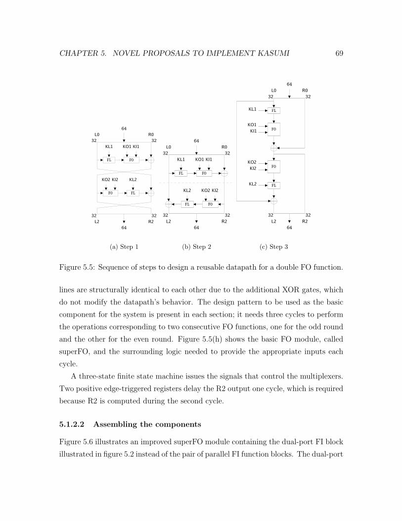
CHAPTER 5. NOVEL PROPOSALS TO IMPLEMENT KASUMI 69
KO1 KI1KL1
FOFL
KO2 KI2
FO
KL2
FL
64
3232L0 R0
R2L232 32
64
(a) Step 1
KO1 KI1KL1
FOFL
3232L0 R0
KO2 KI2
FO
KL2
FL
64
64L2 R2
32 32
(b) Step 2
KL1 FL
KO1KI1 FO
FL
FOKO2KI2
KL2
64
64
3232L0 R0
3232L2 R2
(c) Step 3
Figure 5.5: Sequence of steps to design a reusable datapath for a double FO function.
lines are structurally identical to each other due to the additional XOR gates, which
do not modify the datapath’s behavior. The design pattern to be used as the basic
component for the system is present in each section; it needs three cycles to perform
the operations corresponding to two consecutive FO functions, one for the odd round
and the other for the even round. Figure 5.5(h) shows the basic FO module, called
superFO, and the surrounding logic needed to provide the appropriate inputs each
cycle.
A three-state finite state machine issues the signals that control the multiplexers.
Two positive edge-triggered registers delay the R2 output one cycle, which is required
because R2 is computed during the second cycle.
5.1.2.2 Assembling the components
Figure 5.6 illustrates an improved superFO module containing the dual-port FI block
illustrated in figure 5.2 instead of the pair of parallel FI function blocks. The dual-port

CHAPTER 5. NOVEL PROPOSALS TO IMPLEMENT KASUMI 70
KO1,1 KO1,2
KI1,1
KO1,3
KI1,3
KI1,2
16 16
FI FI
FI
KO2,1 KO2,2
KI2,1
KO2,3
KI2,3
KI2,2
16 16
FI FI
FI
64
3232L0 R0
KL1 FL
FLKL2
16 16
16 16
64L2 R2
3232
(d) Step 4
KO1,1 KO1,2
KI1,1 KI1,2
32
KO1,3
KI1,3
32
1616
1616
KO2,2
KI2,2
KO2,1
KI2,1
KO2,3
KI2,3
KL1
KL2
L0
R0 highR0 low
R2 highR2 low
FL
FI FI
FI
FI
FI FI
L2
FL
(e) Step 5
KO1,1 KO1,2
KI1,1 KI1,2
32
KO1,3
KI1,3
32
1616
1616
KO2,2
KI2,2
KO2,1
KI2,1
KO2,3
KI2,3
KL1
KL2
L0
R0 high
R0 low
R2 high
R2 low
FL
FI FI
FI
FIFI
FI
L2
FL
(f) Step 6
Figure 5.5: Sequence of steps to design a reusable datapath for a double FO function.
(cont.)

CHAPTER 5. NOVEL PROPOSALS TO IMPLEMENT KASUMI 71
KO1,1 KO1,2
KI1,1 KI1,2
32
KO1,3
KI1,3
32
1616
1616
KO2,2
KI2,2
KO2,1
KI2,1
KO2,3
KI2,3
KL2
R0 high
R0 low
R2 high
R2 low
0
0
0
0
KL1 FL
FI FI
FI FI
FI FI
FL
L2
L0
(g) Step 7
16
16
FI1 FI2
KO1,1
KO1,3
KO2,2
KO1,2
R0 high
KO2,3
0
KO2,1
0
KI1,2
KI2,1
KI2,3
KI1,1
KI1,3
KI2,2
0
R0 low
0
16
16
32
32 16
clk
01 0 1
0
1
2
0
1
2
0
1
2
0
1
2
0
1
2
0
1
2
clk
16R2 lowR2 high
(h) Step 8
Figure 5.5: Sequence of steps to design a reusable datapath for a double FO function.
(cont.)

CHAPTER 5. NOVEL PROPOSALS TO IMPLEMENT KASUMI 72
16
KO1,2
R0 high
KO2,3
0
KO2,1
0
0 1
0
1
2
0
1
2
dpFI
KO1,1
KO1,3
KO2,2
16
01
0
1
2
KI1,2
KI2,1
KI2,3
0
1
2
KI1,1
KI1,3
KI2,2
0
1
2
1616
32
32
clk
0
R0 low
0
0
1
2
clk
16
clk
R2 high16
R2 low
clk
clk
Figure 5.6: Datapath for the superFO module including a dual-port FI block.
FI module outputs its results at every positive clock edge, so the additional registers
are needed to delay data, synchronizing them with the outputs of the dpFI module.
Figure 5.7 shows the complete datapath that performs the operations corresponding
to two consecutive rounds. This architecture takes three cycles to complete two
rounds, performs the block ciphering process in 12 cycles, and requires that two
sets of round keys ({KL1, KO1, KI1} and {KL2, KO2, KI2}), corresponding to two
rounds, be available during the three cycles. The control for this datapath consists
of a 12-state finite state machine that sets the multiplexers’ select inputs properly.
5.1.2.3 The key scheduler
The key scheduler for this design must provide the reusable datapath with two sets of
round keys, one for each round, and maintain these sets of keys during three cycles.
The module shown in figure 5.8 meets the requirement of providing two sets of round
keys since it contains two replicas of the components used to generate one set. Adding

CHAPTER 5. NOVEL PROPOSALS TO IMPLEMENT KASUMI 73
0 101
64
32 32
clk
ko1
ki1ko2
ki2superfo
32 32
64
clk
FL
kl2FLkl1
clk
clk
Figure 5.7: Reusable datapath implementing the operations for two rounds.

CHAPTER 5. NOVEL PROPOSALS TO IMPLEMENT KASUMI 74
<<< 5<<< 1
KL1 KO1 KL2 KI2 KI1
<<< 8
KO2 KI3
<<< 13
KO3
K1 K2 K3 K4 K5 K6 K7 K8
C1 C2 C3 C4 C5 C6 C7 C8
O8 O1 O2 O3 O4 O5 O6O7
D8 D1 D2 D3 D4 D5 D6D7
<<< 1
KL1
<<< 5
KO1 KL2 KI2 KI1
<<< 8
KO2
<<< 13
KO3KI3
Firstround
Secondround
Figure 5.8: The key scheduler module for the two-round architecture.
logic to keep the output values during three cycles would be too expensive; therefore,
an alternative solution is conceived. The key scheduler is synchronized with a clock
signal whose frequency is one third the frequency of the overall system’s clock. A
divide-by-three frequency divider, implemented as a three-state finite state machine,
generates the appropriate clock signal for this module. The key scheduler receives the
encryption key K as an array of eight 16-bit input values, which are used to generate
the two sets of round keys, and issues these same values rotated to the left twice every
positive clock edge. The key scheduler module is reused in this project by feeding the
rotated outputs back to the inputs.
5.2 Pipelined design
As in the case of the second reuse-based proposal, the design of the pipelined archi-
tecture also relies on techniques that were developed during the design process of the
previous architectures. The aims of this proposal are to achieve the highest perfor-
mance reported so far for a hardware implementation of the KASUMI block cipher
and to conceive a datapath with short critical path that can be implemented as a
functional unit for a RISC processor.

CHAPTER 5. NOVEL PROPOSALS TO IMPLEMENT KASUMI 75
5.2.1 The datapath
At every clock cycle the architecture receives a plaintext block as input, which is
processed as it goes through the stages that make up the pipeline to produce a
ciphertext block. Several blocks can be processed simultaneously in the different
stages of the datapath. At every clock cycle a ciphertext block leaves the pipeline
from the last stage and the first stage receives a new input plaintext block. This
architecture reaches the best performance owing to the exploitation of temporal and
spatial parallelism when processing plaintext blocks.
The first phase of the design process consists of the manipulations illustrated in
figures 5.5(a)–5.5(f) over a pair of rounds; exactly as shown in the sequence of figures,
no more, no less.
For the second phase consider the two-round datapath in figure 5.5(f); from it, it
is possible to derive the pipelined datapath shown in figure 5.9. At first, each pair
of parallel FI function blocks is replaced by the single dual-port FI module in figure
5.2; in this case three replacements are needed. Next, a couple of registers, a negative
edge-triggered register followed by a positive edge-triggered register, is added in every
line surrounding each dual-port FI block to synchronize the corresponding data with
the two values produced by the dpFI module. The resulting pipeline has four stages,
which means that it requires four cycles to perform two rounds of the ciphering
process. A sequence consisting of four concatenated instances of this pipelined two-
round datapath carries out the whole encryption process with an initial latency of 16
clock cycles.
Since the pipeline stages are independent of each other and have no interdepen-
dencies, the proposed datapath is free of data hazards. Structural hazards do not
exist either because there is not any conflict in the use of hardware resources. Fi-
nally, control hazards are impossible since the architecture does not deal with any
kind of control transfer instruction.
5.2.2 The key scheduler
The key scheduler corresponding to the pipelined datapath described previously is
also designed using a pipelined approach, and must issue the set of round keys corre-

CHAPTER 5. NOVEL PROPOSALS TO IMPLEMENT KASUMI 76
1616
FL
32
L0
KL1
KO1,1 KO1,2
KI1,1 KI1,2
R0 highR0 low
KO1,3
KO2,1
KI2,1KI1,3
dpFI
dpFI
KO2,2 KO2,3
KI2,2 KI2,3
dpFI
32
1616
L2
FLKL2
R2 low
16
R2 high
16
Figure 5.9: Pipelined datapath for the two-round sequence.

CHAPTER 5. NOVEL PROPOSALS TO IMPLEMENT KASUMI 77
sponding to the odd round and the set of round keys corresponding to the even round
in the following order:
Clock cycle 1: The key scheduler generates the 32-bit long KL1 round key and the
32 most significant bits of both the KO1 and KI1 round keys, i.e. KO1,1||KO1,2
and KI1,1||KI1,2.
Clock cycle 2: The key scheduler generates the 16 least significant bits of both the
KO1 and KI1 round keys, i.e. KO1,3 and KI1,3, as well as the 16 most significant
bits of both the KO2 and KI2 round keys, i.e. KO2,1 and KI2,1.
Clock cycle 3: The key scheduler generates the 32 least significant bits of both
the KO2 and KI2 round keys, i.e. the key scheduler issues KO2,2||KO2,3 and
KI2,2||KI2,3.
Clock cycle 4: The key scheduler generates the 32-bit long KL2 round key.
Figure 5.10 shows the organization of the key scheduler just described. Notice that
its pipelined design enables it to compute the round keys for different plaintext blocks
during the same clock cycle. In addition, each stage of the key scheduler computes
only the round keys, or the portion of them, that are required by the corresponding
stage in the ciphering datapath and no more. As the key scheduler in figure 5.8,
this design also rotates the input arrays two positions to the left and outputs the
resulting arrays, so the following instance receives the correct values and generates
the appropriate sets of round keys for the next two-round sequence.
5.3 Reuse-based architecture 3
The strategy consists of iterating several times over a datapath implementing only
a fraction of the whole block cipher discussed in the previous section, feeding back
the output to the input, until completion of the process. This scheme is appropriate
when the goal of the implementation is to save hardware resources, sacrificing perfor-
mance. The architecture for this approach, unlike the pipelined one, does not receive
a plaintext block each clock cycle, so there is no temporal parallelism. There is still
spatial parallelism between the components of the datapath though.

CHAPTER 5. NOVEL PROPOSALS TO IMPLEMENT KASUMI 78
KL1,1 KO1,1 KL1,2 KI1,2 KI1,1 KO1,2
K1 K2 K3 K4 K5 K6 K7 K8
C1 C2 C3 C4 C5 C6 C7 C8
KO1,3KO2,1 KI1,3KI2,1
KO2,2 KO2,3KI2,2KI2,3
KL2,2KL2,1
O8 O1 O2 O3 O4 O5 O6O7
D8 D1 D2 D3 D4 D5 D6D7
<<< 1
<<< 8 <<< 13
<<< 5 <<< 13
<<< 1 <<< 5 <<< 8
Figure 5.10: Pipelined key scheduler.

CHAPTER 5. NOVEL PROPOSALS TO IMPLEMENT KASUMI 79
5.3.1 The datapath
The basic block for the new architecture is the datapath in figure 5.9, although
not used in a pipelined fashion. A multiplexer is placed at each of the L0 and R0
input ports; these multiplexers select the input to the datapath from two options:
a new input plaintext block and the output value L2||R2, which is fed back to the
datapath’s input. A plaintext block travels alone through the datapath every clock
cycle, requiring four clock cycles to reach the end of the two-round datapath and 16
cycles to complete the iterative eight-round ciphering process.
5.3.2 The key scheduler
This architecture requires the design of a new key scheduler that issues and maintains
the set of round keys for the first round ({KL1, KO1, KI1}) along with the 16 most
significant bits of the KO2 and KI2 round keys during two cycles. In addition, during
the next two cycles it must issue and maintain the rest of the round keys for the second
round, i.e. the 32 least significant bits of the KO2 and KI2 round keys, as well as
the KL2 round key. Figure 5.11 illustrates the key scheduler designed to meet these
requirements. It contains two left-rotate registers: one register stores the array of
eight 16-bit subkeys (Ki, 1 ≤ i ≤ 8) that make up the encryption key K and the
second register stores the array of fixed constants (Ci, 1 ≤ i ≤ 8) used to generate
the round keys. Both of these registers are synchronized with a divide-by-two clock
divider that allows the contents of the registers to be available during two clock cycles
before being shifted. The registers must be preloaded with the encryption key K and
the array of constants before any ciphering process is carried out; this preloading
needs 16 clock cycles and must be performed every time the encryption key changes.
5.4 Implementation and results
As mentioned at the beginning of this chapter, the implementation process was car-
ried out using the VHDL language to build synthesizable cores of the designs and the
FPGA technology to get a functional hardware prototype. Each of the designs was
successfully verified using the four tests described in [6]. This phase of the project
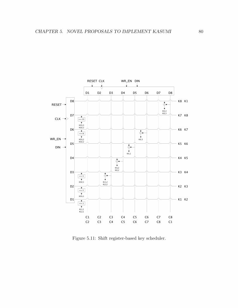
CHAPTER 5. NOVEL PROPOSALS TO IMPLEMENT KASUMI 80
<<< 8
<<< 5
<<< 1
<<< 13
KI1,3
KO1,3
KO1,2
KI1,1
KI1,2
KL1,2
KO1,1
KL1,1
KI2,1
KO2,1
<<< 5
K8
K7
K6
K5
K4
K3
K2
K1
K8
K7
K6
K5
K4
K3
K2
K1
C1 C2 C3 C4 C5 C6 C7 C8
C1C2 C3 C4 C5 C6 C7 C8
KL2,1
KL2,2
KO2,2
KO2,3
KI2,2
KI2,3
DINWR_ENCLKRESET
D1 D2 D3 D4 D5 D6 D7 D8
DIN
WR_EN
CLK
RESET
D1
D2
D3
D4
D5
D6
D7
D8
Figure 5.11: Shift register-based key scheduler.
CHAPTER 5. NOVEL PROPOSALS TO IMPLEMENT KASUMI 81
provided an important amount of information concerning the operation of the archi-
tectures, their performance and the number of resources consumed.
To make fair comparisons with the architectures described in chapter 3, the designs
described here were also implemented in FPGA devices belonging to the Virtex-E
family from Xilinx and synthesized using the Xilinx Synthesis Technology (XST)
software tools [35, 36].
5.4.1 Platform description
The elements of every Virtex-E device are: the CLBs, which are the building blocks
used to assemble a complete digital system; the Input/Output Blocks (IOBs) that
provide the interface between the packet’s pins and the CLBs; the embedded memory
blocks; the Delay Lock Loops (DLL), which are digital circuits intended to perform
clock management functions such as clock-distribution and delay compensation; and
the static configuration memory.
Each Virtex-E CLB contains two slices that are made up of two Logic Cells (LCs),
so there is a total number of four LCs per CLB. Figure 5.12 shows the organization of
the two LCs comprising every slice. Each LC contains a four-input function generator
implemented as a four-input lookup table (LUT), dedicated elements for logic opera-
tions such as XOR and AND, dedicated carry paths, a flip-flop storage element and
logic that combines the outputs of the function generators to implement functions of
more inputs.
The Virtex-E devices introduce large blocks of BRAM memories. Each of these
blocks is a fully synchronous dual-port (True Dual Port) 4096-bit RAM with indepen-
dent control signals for each port. The data widths of the two ports can be configured
in an independent fashion.
5.4.2 Synthesis results
Table 5.1 shows the results of the synthesis process concerning utilization of the
FPGA’s internal resources for the four designs described in the previous section.
Notice that the percentage of resources in the reconfigurable fabric, i.e. slices, flip-
flops and LUTs, required by the reuse-based architectures does not surpass 20%.

CHAPTER 5. NOVEL PROPOSALS TO IMPLEMENT KASUMI 82
Figure 5.12: Organization of a Virtex-E slice.
Also notice that the pipelined proposal occupies less than one-third of the hardware
resources of the FPGA where it was implemented. This is an indication of how
compact the architectures are and a proof of the efficient use of the resources in the
FPGA.
To make fair comparisons with most of the synthesis results provided for the
other proposals, the designs were synthesized for devices with a speed grade of -8.
The optimization goal was set to speed.
Consider the number of bits needed to implement each S-box: 128× 7 = 896 bits
for each S7 S-box and 512×9 = 4608 bits for each S9 S-box. A S7 S-box fits well in a
4096-bit BRAM block, whereas a 4608-bit S9 S-box is far larger; therefore, two blocks
are required to implement one S9 dual-port S-box. That is why in our proposals each
dpFI module needs six BRAM blocks to implement the S-boxes instead of only four.
The use of BRAM blocks removes complexity from the reconfigurable fabric.

CHAPTER 5. NOVEL PROPOSALS TO IMPLEMENT KASUMI 83
Pro
posa
lD
evic
eC
ate
gory
Num
ber
of
Tota
lnum
ber
of
Per
centa
ge
elem
ents
use
del
emen
tsavailable
ofuse
Reu
se-b
ase
ddes
ign
1X
CV
300E
-8-B
G432
Slice
s488
3072
15%
Slice
Flip-F
lops
566
6144
9%
4-input
LU
Ts
898
6144
14%
BR
AM
s6
32
18%
GC
LK
s1
425%
Reu
se-b
ase
ddes
ign
2X
CV
300E
-8-B
G432
Slice
s566
3072
18%
Slice
Flip-F
lops
546
6144
8%
4-input
LU
Ts
1014
6144
16%
BR
AM
s6
32
18%
GC
LK
s1
425%
Reu
se-b
ase
ddes
ign
3X
CV
300E
-8-B
G432
Slice
s625
3072
20%
Slice
Flip-F
lops
1018
6144
16%
4-input
LU
Ts
649
6144
10%
BR
AM
s18
32
56%
GC
LK
s1
425%
Pip
elin
eddes
ign
XC
V1000E
-8-B
G560
Slice
s3928
12288
31%
Slice
Flip-F
lops
6596
24576
26%
4-input
LU
Ts
2146
24576
8%
BR
AM
s72
96
75%
GC
LK
s1
425%
Tab
le5.
1:Sum
mar
yof
the
synth
esis
resu
lts
for
the
arch
itec
ture
spro
pos
ed.

CHAPTER 5. NOVEL PROPOSALS TO IMPLEMENT KASUMI 84
5.5 Comparison
Table 5.2 is a summary of the relevant data concerning performance and area com-
plexity for all of the FPGA implementations of the KASUMI algorithm considered
so far. The throughput of the architectures developed for this project was computed
by using the expression (3.1) for the iterative designs and the expression (3.2) for the
pipelined proposal. The table illustrates that some throughput values reported for
other proposals do not agree with the expressions, perhaps due to a miscalculation;
these values are indicated in the table.
The reuse-based architecture with the highest performance is the hybrid design
proposed in [21]; it achieves a throughput of 432 Mbps, at the expense of a great
number of slices though. The second place is for the third iterative architecture
developed for this project, which with 5.5 times fewer slices it achieves almost 73.6%
of the hybrid design’s performance.
There is no any comment in [29] about the design of the architecture with a la-
tency of eight clock cycles, only its results; however, its performance is good and
even surpasses this project’s second reuse-based proposal in this respect. Notice that
although our proposal’s clock frequency (41.63 MHz) is higher than the other archi-
tecture’s clock frequency (33.14 MHz), its longer latency (12 clock cycles) decreases
its performance. Notice that the difference between the number of slices required by
our design and the number of slices occupied by the other proposal is very small: 22
slices.
Assume that the throughput of the hybrid architecture reported in [20] (Type 2),
and illustrated in table 5.2, is correct. In that case the conclusion is that the second
iterative design proposed in this document, the one with a latency of 12 clock cycles,
has a very competitive performance consuming fewer hardware resources. It is a good
tradeoff between high performance and low area complexity.
Now consider the two simplified architectures proposed in [29] and illustrated in
figure 3.3. Table 5.2 indicates that their performance is lower than our first reuse-
based architecture’s performance, even though they have higher clock frequencies and
consume fewer slices. This is a clear indication that the design of architectures having
long latencies should be avoided, privileging instead tradeoffs between short latency

CHAPTER 5. NOVEL PROPOSALS TO IMPLEMENT KASUMI 85
Hard
ware
Pro
posa
lA
ppro
ach
Late
ncy
Are
aFre
quen
cyT
hro
ughput
effici
ency
Num
ber
of
Num
ber
of
Dev
ice
(cycl
es)
(slice
s)(M
Hz)
(Mbps)
(kbps/
slic
es)
S-b
oxes
BR
AM
s
Work
sin
[29]
Reu
se56
368
68.1
377.8
6211.5
82
N/A
bX
CV
300E
-8-B
G432
Reu
se32
370
58.0
6116.1
2313.8
44
N/A
bX
CV
300E
-8-B
G432
Reu
se8
588
33.1
4265.1
2450.8
812
N/A
bX
CV
300E
-8-B
G432
Work
sin
[24]
Reu
se40
749
35.3
570.7
0d
94.3
924
24
eX
CV
200E
-6-F
G456
Pip
elin
e40
a2213
37.7
22414.0
81090.8
696
96
eX
CV
1000E
-6-B
G560
Work
sin
[20]
Reu
se8
650
20
110
d169.2
312
N/A
bN
/A
c
Hybri
d32
1100
33
234
d212.7
312
N/A
bN
/A
c
Work
sin
[21]
Pip
elin
e8
a9476
f56
3584
378.2
296
N/A
bX
CV
300E
-8-B
G432
Hybri
d8
3452
f54
432
125.1
424
N/A
bX
CV
300E
-8-B
G432
Thes
ew
ork
sR
euse
16
488
41.1
4164.5
6337.2
14
6X
CV
300E
-8-B
G432
Reu
se12
566
41.6
3222.0
2392.2
64
6X
CV
300E
-8-B
G432
Reu
se16
625
79.4
5317.8
508.4
812
18
XC
V300E
-8-B
G432
Pip
elin
ed16
a3928
83.1
45320.9
61354.6
248
72
XC
V1000E
-8-B
G560
aIn
itia
lla
tency
,once
the
pip
elin
eis
filled
the
arc
hit
ectu
repro
duce
sa
cipher
text
blo
ckea
chcy
cle.
bN
ot
applica
ble
.c
Info
rmati
on
not
available
.d
Valu
ere
port
edin
the
corr
espondin
gre
fere
nce
that
does
not
agre
ew
ith
expre
ssio
n(3
.1).
eT
his
seem
sto
be
wro
ng
since
two
BR
AM
sare
nee
ded
for
each
S9
S-b
ox.
fIn
form
ati
on
ori
gin
ally
pro
vid
edin
term
sofC
LB
s:4738
for
the
pip
elin
eddes
ign
and
1726
for
the
reuse
-base
ddes
ign.
The
XC
V300E
dev
ice
only
conta
ins
1536
CLB
s.
Tab
le5.
2:Sum
mar
yof
info
rmat
ion
conce
rnin
gper
form
ance
and
har
dw
are
com
ple
xity
for
the
diff
eren
tar
chit
ectu
res
imple
men
ting
the
KA
SU
MI
blo
ckci
pher
inFP
GA
tech
nol
ogy.

CHAPTER 5. NOVEL PROPOSALS TO IMPLEMENT KASUMI 86
and a reasonable number of hardware resources. The iterative designs in [20] and [24]
do not do better either; as well as being more expensive in terms of FPGA resources,
their performance is poorer, almost 1.5 times lower in the first case and 2.3 times
lower in the second case.
The higher clock frequencies of the third iterative design and the pipelined design
proposed here are explained by the short critical path of these architectures. There
are very few logic components between each pair of registers, including the negative
edge-triggered and the positive edge-triggered, located throughout the datapath of
both the cipher and the key scheduler. The difference between the clock frequencies
of these two designs is due to the long feedback signal paths and the two multiplexers
added to the L0 and R0 input ports in the third reuse-based architecture, which are
required to enable the reuse of the ciphering datapath.
The pipelined architecture proposed here is superior to the pipelined designs in
[21] and [24] because the optimizations performed on the Feistel structure and the
mapping of the S-boxes to embedded memory blocks produce a short critical path
that increases the overall clock frequency and, as indicated by the expression (3.2),
the throughput, which is the highest reported so far. Also, our design is almost 2.5
times cheaper in terms of FPGA resources, or slices, than the architecture reported
in [21], which is a consequence of a lack of optimization efforts and the inclusion of
pure combinational S-boxes in that proposal.

Chapter 6
The extended processor core
This chapter describes the extensions made to a MIPS-based processor core to sup-
port block ciphering according to the KASUMI algorithm. The information provided
includes a thorough description of the components of the new functional unit and
the four instructions added to the instruction set, an accurate timing analysis and
implementation results for a FPGA platform.
6.1 The base processor core
The first task is to select the most suitable processor core to extend according to very
specific requirements. The following is a description of such requirements:
Availability of the source code. The goal of this project is not only to propose
the organization and operation of the functional unit, but also to actually carry
out the integration process. That is why it is strictly necessary to have the
source code of the core.
Functionality. The processor core to use should have been employed previously to
solve practical problems.
Simplicity. A high performance processor like those designed for the workstation
market is so complex to be used in an embedded environment like the one con-
sidered in this project. Therefore, the processor core to use shall not contain
87

CHAPTER 6. THE EXTENDED PROCESSOR CORE 88
complexities like Memory Management Units (MMUs), complex branch predic-
tion and prefetching algorithms, an elaborated memory hierarchy and floating
point execution units.
A commercial or open source processor core can be classified into one of two categories:
extendible or configurable.
The designer is able to add functionality to an extensible core when its source
code, written in a hardware description language, is available. In some cases a front-
end application allows to specify the values for some parameters in the source code.
In addition to extending the processor model, the designer must modify the compiler
and other system software tools in order for them to know about the new extensions.
Some examples are: MIPS32 M4KTMfor MIPS and LEON2 for SPARC V8.
Configurable cores allow designers to specify the necessary functionality and re-
move the unneeded features by means of advanced software tools. It is also possible
to extend their functionality in a similar way as for extensible cores. In both cases the
designer configures the processor by means of software, which at the end generates
the source code for the core as well as its compiler, simulator and debugger. Some
examples are: ARCTM700 from ARC International and Xtensa from Tensilica Inc.
Due to budget limitations it was not possible to use a commercial configurable
core since the start of the project, so the first important decision was to employ an
open source extensible core. The use of a very complex core to carry out the job is
feasible, but the time needed to understand the core’s internals and conceive a way
to extend it increases noticeably. Therefore, the simplicity of the source code is a
key factor to make the final decision. The core chosen for this project that meets
the requirements is the MyRISC core [34], which models a MIPS processor with the
following features:
• Implements the R2000 32-bit instruction set.
• Its five-stage pipeline structure is identical to that described in [18].
• Does not include a memory hierarchy, although it is possible to add it.

CHAPTER 6. THE EXTENDED PROCESSOR CORE 89
6.2 The KASUMI functional unit
Figure 6.1 shows the organization of the extended MyRISC core proposed. The part
above the thick horizontal line corresponds to the initial RISC processor core as it is
distributed. The components lying below the thick line correspond to the KASUMI
extension, which carries out the processing corresponding to two rounds.
A detailed description of the components of the functional unit is provided next.
Figure 6.1 illustrates that the modules that store and generate data operands are
located in the processor’s Instruction Decode (ID) stage, whereas the modules that
perform encryption operations belong to the Execute (EX) stage.
6.2.1 The extended register file
The new functional unit contains ten 32-bit registers that store the data it processes.
Extended instructions move data from/to integer registers to/from a register within
this new register file. Figure 6.2 shows the organization of this data unit.
Registers 0 and 1 store the plaintext block the KASUMI functional unit works
with; after the ciphering process the registers store the ciphertext block produced.
The 32 most significant bits of the block are stored in register 0, whereas register 1
stores the 32 least significant bits. The 128-bit encryption key K is split into four 32-
bit parts and stored in registers 2 to 5. Registers 6 to 9 store the ciphering constants
used along with the encryption key to generate the set of round keys KLi, KOi, KIi
for each round i. There is no need to preload the array of constants since these values
are automatically stored every time the RESET signal is asserted.
Any of the first six registers within the extended register file can be synchronously
written by specifying its address and the value to store, in the same way as for integer
registers. Registers 0 and 1 can be written in parallel to store the ciphertext block
produced by the block ciphering modules. These two kinds of writing can not be
accomplished simultaneously.
The array that stores the encryption key K (registers 2 to 5) is synchronously
rotated upwards to compute the appropriate round keys for the next two rounds.
This is also true for the array that stores the ciphering constants (registers 6 to 9).

CHAPTER 6. THE EXTENDED PROCESSOR CORE 90
Fig
ure
6.1:
The
MyR
ISC
MIP
S-b
ased
pro
cess
orco
rew
ith
the
exte
nded
KA
SU
MI
funct
ional
unit
.

CHAPTER 6. THE EXTENDED PROCESSOR CORE 91
L
R
031
K1 || K2
K3 || K4
K5 || K6
K7 || K8
C1 || C2
C3 || C4
C5 || C6
C7 || C8
0
1
2
3
4
5
6
7
8
9
LOUT
ROUT
KOUT0
KOUT1
KOUT2
KOUT3
COUT0
COUT1
COUT2
COUT3
DOUT
RESETCLK
DIN
ADDR
WE
LIN
RIN
PWE
RDADDR
SE
Figure 6.2: The organization of the extended KASUMI register file.
The only kind of writing allowed to occur at the same time as the rotation of the
arrays is the parallel writing of registers 0 and 1.
The register file asynchronously outputs the contents of the ten internal registers.
An additional output issues the contents of a specific register indicated by an input
address line in an asynchronous fashion as well.
6.2.2 The forwarding unit
This module allows the KASUMI functional unit to use correct and up-to-date values
of the plaintext block and the encryption key. The extended processor allows different
instructions that modify the first six registers to be executing along the pipeline. The
forwarding unit receives values from the KASUMI register file and from different
pipeline stages and determines if the values stored in registers are old, in which case
the unit outputs the new values before they are actually written in the extended
register file. This unit makes its decision based on input control signals and register
address lines coming from either the stages in the integer pipeline or the modules
comprising the KASUMI functional unit.
The forwarding unit outputs the plaintext block sent to the extended register
CHAPTER 6. THE EXTENDED PROCESSOR CORE 92
file most recently, or the ciphertext block computed most recently, directly to the
ID/EX pipeline register. The outputs corresponding to the encryption key are used
to generate the next two sets of round keys.
6.2.3 The key generation unit
The KASUMI functional unit attached to the processor core carries out two rounds of
the whole ciphering process. The key generation unit outputs two sets of round keys
({KL1, KO1, KI1} and {KL2, KO2, KI2}) and stores them into the ID/EX pipeline
register to be issued to the ciphering datapath during the next clock cycle.
This unit receives as inputs the four 32-bit words comprising the encryption key
K from the forwarding logic and the four 32-bit words storing the ciphering con-
stants from the extended register file. The round keys are generated according to the
procedure illustrated in table 2.1.
6.2.4 The ciphering datapath
This module is parallel to the EX stage of the processor’s datapath and performs
the encryption process using the block issued by the forwarding unit and the round
keys computed by the key generation unit. It carries out two rounds of the KASUMI
algorithm in four steps: K1, K2, K3 and K4, where each step takes one clock cycle to
complete. In spite of this multicycle operation, the ciphering datapath is not intended
to work in a pipelined fashion. This means that an instruction that uses the ciphering
datapath is not allowed to enter the K1 module until the previous instruction has left
the K4 module. In the KASUMI functional unit illustrated in figure 6.1 synchronous
registers are indicated by grey boxes.
At this point of the project it is possible to take advantage of the work carried
out previously, so the basic two-round datapath in figure 6.3 is used to implement
the ciphering datapath attached to the processor core and shown in figure 6.1.
When the ciphering process reaches the K3 module it commands the KASUMI
register file to rotate the arrays storing the encryption key and the ciphering constants,
by means of a control signal indicated by a dashed line in figure 6.1, in order for the

CHAPTER 6. THE EXTENDED PROCESSOR CORE 93
1616
FL
32
L0
KL1
KO1,1 KO1,2
KI1,1 KI1,2
R0 highR0 low
KO1,3
KO2,1
KI2,1KI1,3
dpFI
dpFI
KO2,2 KO2,3
KI2,2 KI2,3
dpFI
32
1616
L2
FLKL2
R2 low
16
R2 high
16
K1
K2
K3
K4
Figure 6.3: Pipelined datapath for the two-round sequence.

CHAPTER 6. THE EXTENDED PROCESSOR CORE 94
next two sets of round keys to be available in the next two clock cycles, when a new
instruction enters K1.
During the K4 step the corresponding module bypasses the computed ciphertext
block to the forwarding unit to override the block stored in registers and make the
new one available as the plaintext block to process in the next clock cycle. A control
signal indicated by a dashed line in figure 6.1 is also bypassed to help the forwarding
unit to determine the correct value of the block.
When the ciphering instruction leaves the K4 module it enters the pipeline’s mem-
ory access stage (MEM) where, in the case of KASUMI instructions, the ciphertext
block just computed is actually written into registers 0 and 1 within the extended
register file. Meanwhile, a new KASUMI ciphering instruction can start with the K1
step.
6.3 The extended instructions
This section describes the four instructions added to the MIPS instruction set that
exploit the KASUMI functional unit. Information concerning instruction formats and
the effects on the processor’s state is provided.
6.3.1 The kxor1 instruction
MNEMONIC: kxor1 KRd, Rs, Rt.
DESCRIPTION: Carries out the operation Rs⊕Rt, where Rs and Rt are integer
registers. This instruction uses the integer EX and MEM pipeline stages and
saves the result in the extended KASUMI register file at the entry addressed by
the four least significant bits of KRd during the integer WB stage.
FORMAT: This instruction is encoded using the R-format, i.e. the op field equals
0000002. The value assigned to the funct field is 1010 = 0010102, which con-
veniently sets the processor’s control signals to appropriately drive the flow of
data along the datapath to accomplish the instruction. The value of the shamt
field is discarded. Figure 6.4 summarizes this information.

CHAPTER 6. THE EXTENDED PROCESSOR CORE 95
31 2625 2120 1615 1110 6 5 0000000 Rs Rt KRd X 001010
R-format:
Figure 6.4: Format of the kxor1 instruction.
31 2625 2120 1615 1110 6 5 0000000 Rs KRt KRd X 001011
R-format:
Figure 6.5: Format of the kxor2 instruction.
6.3.2 The kxor2 instruction
MNEMONIC: kxor2 KRd, Rs, KRt
DESCRIPTION: Carries out the operation Rs ⊕ KRt, where Rs is an integer
register and KRt is a register in the extended KASUMI register file. This
instruction uses the integer EX and MEM pipeline stages and saves the result
in the extended KASUMI register file at the entry addressed by the four least
significant bits of KRd during the integer WB stage.
FORMAT: This instruction is encoded using the R-format, i.e. the op field equals
0000002. The value assigned to the funct field is 1110 = 0010112, which con-
veniently sets the processor’s control signals to appropriately drive the flow of
data along the datapath to accomplish the instruction. The value of the shamt
field is discarded. Figure 6.5 summarizes this information.
6.3.3 The kxor3 instruction
MNEMONIC: kxor3 Rd, Rs, KRt
DESCRIPTION: Carries out the operation Rs ⊕ KRt, where Rs is an integer
register and KRt is a register in the extended KASUMI register file. This
instruction uses the integer EX and MEM pipeline stages and saves the result
in the integer register addressed by Rd during the integer WB stage.

CHAPTER 6. THE EXTENDED PROCESSOR CORE 96
31 2625 2120 1615 1110 6 5 0000000 Rs KRt Rd X 110010
R-format:
Figure 6.6: Format of the kxor3 instruction.
FORMAT: This instruction is encoded using the R-format, i.e. the op field equals
0000002. The value assigned to the funct field is 5010 = 1100102, which con-
veniently sets the processor’s control signals to appropriately drive the flow of
data along the datapath to accomplish the instruction. The value of the shamt
field is discarded. Figure 6.6 summarizes this information.
6.3.4 The k2rnd instruction
MNEMONIC: k2rnd
DESCRIPTION: This instruction carries out the operations corresponding to a
sequence of an odd round and an even round of the KASUMI block cipher. It
does not need explicit operands; it uses the outputs of the forwarding logic and
the key generation unit. A sequence of four k2rnd instructions performs the
whole KASUMI algorithm.
k2rnd is a multicycle instruction whose execution phase is actually made up of
four cycles: K1, K2, K3 and K4. Only after a k2rnd instruction has finished
with cycle K4, the next k2rnd instruction will enter K1.
During the MEM stage this instruction issues the computed block to the ex-
tended register file in order for it to be stored in registers 0 and 1. Since this
operation is synchronous, the block is actually written when the instruction
enters the WB stage.
FORMAT: This instruction is encoded using the I-format with op = 4410 = 1011002.
The rest of the instruction fields, i.e. Rs, Rt and the immediate value, are
discarded. See figure 6.7.

CHAPTER 6. THE EXTENDED PROCESSOR CORE 97
31 2625 2120 1615 0101100 X X X
I-format:
Figure 6.7: Format of the k2rnd instruction.
6.4 Details about the execution of extended in-
structions
Figure 6.8 illustrates the pipelined execution of the instructions making up the en-
cryption process. The operands of the instructions are carefully chosen to show how
the extended processor deals with special execution conditions.
The first six kxor1 instructions load the plaintext block and the encryption key
into the extended registers. The next four k2rnd instructions perform the encryption
process using the operands stored by the previous instructions.
Notice that the address of the target register in instruction 1, which is 0, equals the
address of the first source register in instruction 2. For integer instructions this would
cause a data hazard and the bypassing of the value computed by instruction 1 in the
EX stage to the ID stage of instruction 2 during the third clock cycle. However, for
the instructions in figure 6.8 the bypassed value is ignored by the integer forwarding
logic since the target register of instruction 1 is an extended register, not an integer
register as the source register of instruction 2. This situation is called a false data
hazard and is handled by the processor by appropriately setting a control signal. The
same situation occurs during cycles 4 and 5.
A true data hazard occurs during the eighth cycle because the first k2rnd instruc-
tion needs to compute the two sets of round keys and, at this time, the encryption
key K has not been completely stored. However, the forwarding logic in the KA-
SUMI functional unit overcomes this problem. This module receives the bypassed
data signals from the kxor1 instructions in the EX, MEM and WB stages of the
integer pipeline and issues them to the key generation unit to produce the round keys
needed in the next cycle. The KASUMI forwarding logic ignores any bypassed signal
issued by an instruction different from kxor1 and kxor2.

CHAPTER 6. THE EXTENDED PROCESSOR CORE 98
Fig
ure
6.8:
Pip
elin
edex
ecuti
onof
ase
quen
ceof
exte
nded
inst
ruct
ions.

CHAPTER 6. THE EXTENDED PROCESSOR CORE 99
Figure 6.8 shows how the pipeline is stalled to prevent a k2rnd instruction from
entering K1 before a previous k2rnd instruction leaves K4. It does not make sense to
allow the pipelined execution of the two instructions due to, for instance, the block
the instruction 8 is going to work with is not ready when the instruction 7 enters K2.
Notice in figure 6.8 that the overlapped execution of a k2rnd instruction (10) and
an integer instruction (11) is allowed. This situation does not produce structural
hazards since the integer MEM and WB stages do not share any module with the
corresponding MEM and WB stages in the extended functional unit. When a k2rnd
instruction, e.g. the instruction 7 in figure 6.8, enters K1 a no-operation integer
instruction enters EX in the integer portion of the processor’s pipeline.
The number of cycles elapsed since instruction 7 starts execution until instruction
10 leaves the execution stage is 16 cycles. A total number of 26 cycles are needed
to carry out the whole ciphering process including the storage of the plaintext block
and the encryption key into the extended register file.
6.5 Comparison with an implementation in soft-
ware
This section highlights the advantages of the integration approach just described by
demonstrating that the number of instructions needed to implement the KASUMI
block cipher in software, using the standard MIPS32 instruction set, is much higher
than the number of extended instructions needed. As a consequence, the number of
clock cycles a non-extended MIPS processor requires is much higher than the number
of cycles the extended MIPS processor invests.
The C code for KASUMI included in [5] is made up of five functions: FI(), FO(),
FL(), KeySchedule() and Kasumi(). This code is suitable to carry out a thorough
study concerning the number of instructions executed by a compiled program. The
source code is compiled using the C cross-compiler provided by the Software Develop-
ment Environment (SDE) for MIPS-based products toolkit from MIPS Technologies
[26], which is actually a built of GNU’s C compiler. The compiler is instructed, with
the -Os option, to enable all the optimizations intended to reduce code size and gen-

CHAPTER 6. THE EXTENDED PROCESSOR CORE 100
FI( )
Length: 34 instructions
Number of load instructions: 4
lhu: 4
Number of store instructions: 0
Number of arithmetic and logic instructions: 29
Number of control transfer instructions: 1
Number of function calls: 0
Number of loops: 0
Number of if-then-else structures: 0
Total number of instructions executed by the function: 34
Table 6.1: Instruction analysis for the FI() function.
erate the shortest executable program. This executable program is then disassembled
using the objdump utility, which displays information from object files and is part of
the GNU’s set of binary utilities (Binutils).
The result of the study is summarized in tables 6.1–6.5. The instructions making
up each module are counted, special constructs like loops, control transfer statements
and function calls are identified and a precise counting of executed instructions is
carried out for each of these constructs. The last entry of the tables provides the exact
number of instructions the MIPS processor executes for the corresponding function.
The number of instructions required to perform the KASUMI algorithm is given
by adding the counts for the top level modules Kasumi() and KeySchedule(), i.e.
1540 + 915 = 2455 instructions.
The proposal described in this document only requires ten instructions to perform
the block ciphering process. It also requires a few load instructions to transfer the
values employed to compute the plaintext block and the encryption key from memory
to the integer registers. A few more instructions may be needed if it is necessary to
move the ciphertext block to the integer register file and from there to memory. Con-
sidering these facts, a few tens of instructions would be required to have a ciphertext
block stored in the system’s memory. The new approach proposed allows to reduce
the number of instructions required by two orders of magnitude at the expense of the
addition of a compact functional unit.

CHAPTER 6. THE EXTENDED PROCESSOR CORE 101
FO()
Length: 51 instructions
Number of load instructions: 9
lhu: 6
lw: 3
Number of store instructions: 3
sw: 3
Number of arithmetic and logic instructions: 35
Number of control transfer instructions: 4
Number of function calls: 3
Call 1: FI()
Number of instructions executed: 34
Call 2: FI()
Number of instructions executed: 34
Call 3: FI()
Number of instructions executed: 34
Total number of instructions executed: 102
Number of loops: 0
Number of if-then-else structures: 0
Total number of instructions executed by the function: 153 instructions
Table 6.2: Instruction analysis for the FO() function.
FL()
Length: 24 instructions
Number of load instructions: 2
lhu: 2
Number of store instructions: 0
Number of arithmetic and logic instructions: 21
Number of control transfer instructions: 1
Number of function calls: 0
Number of loops: 0
Number of if-then-else structures: 0
Total number of instructions executed by the function: 24
Table 6.3: Instruction analysis for the FL() function.

CHAPTER 6. THE EXTENDED PROCESSOR CORE 102
Kasumi()
Length: 70 instructions
Number of load instructions: 14
lbu: 8
lw: 6
Number of store instructions: 14
sb: 8
sw: 6
Number of arithmetic and logic instructions: 36
Number of control transfer instructions: 6
Number of loops: 1
Loop 1:
Number of iterations: 4
Length of the body of the loop: 18 instructions
Number of function calls: 4
Call 1: FL()
Number of instructions executed: 24
Call 2: FO()
Number of instructions executed: 153
Call 3: FO()
Number of instructions executed: 153
Call 4: FL()
Number of instructions executed: 24
Total number of instructions executed by the four functions: 354
Length of the body of the loop including the four functions: 372 instructions
Total number of instructions executed by the loop: 1488
Number of instructions outside the loop: 52 instructions
Number of if-then-else structures: 0
Total number of instructions executed by the function: 1540 instructions
Table 6.4: Instruction analysis for the Kasumi() function.

CHAPTER 6. THE EXTENDED PROCESSOR CORE 103
KeySchedule()
Length: 138 instructions
Number of load instructions: 23
lbu: 2
lhu: 10
lw: 11
Number of store instructions: 21
sh: 10
sw: 11
Number of arithmetic and logic instructions: 90
Number of control transfer instructions: 4
Number of loops: 3
Loop 1:
Number of iterations: 8
Length of the body of the loop: 9 instructions
Total number of instructions executed by the loop: 72
Loop 2:
Number of iterations: 8
Length of the body of the loop: 14 instructions
Total number of instructions executed by the loop: 112
Loop 3:
Number of iterations: 8
Length of the body of the loop: 88 instructions
Total number of instructions executed by the loop: 704
Total number of instructions executed by the three loops: 888
Number of instructions outside de loops: 27 instructions
Number of if-then-else structures: 0
Total number of instructions executed by the function: 915 instructions
Table 6.5: Instruction analysis for the KeySchedule() function.

CHAPTER 6. THE EXTENDED PROCESSOR CORE 104
Category ID K1 K2 K3 K4
Number of Slices 2113 174 137 100 37
Number of Slice Flip Flops 2015 303 239 174 65
Number of 4 input LUTs 3885 109 125 125 64
Number of BRAMs 0 6 6 6 0
Maximum Frequency (MHz) 100.725 96.339 96.339 96.339 Not found
Table 6.6: Synthesis results for the components of the KASUMI functional unit.
6.6 Synthesis results
Table 6.6 summarizes the information provided by the XST tools concerning the num-
ber of hardware resources in the FPGA consumed by the different modules making up
the KASUMI functional unit. The column labeled ID refers to the set of components
that constitute the instruction decode stage, both the logic elements located in the
integer portion and those located in the extended functional unit.
The synthesis process was carried out using a XCV1000E-8BG560 Virtex-E device,
which contains 12288 slices, 24576 slice flip-flops, 24576 four-input LUTs and 96
SelectRAM+ memory blocks. Notice that the percentage of use of hardware resources
for every module listed in table 6.6 is low, not surpassing 17% in the case of the
number of slices required and 15% in the case of the number of four-input LUTs in
the reconfigurable fabric.
Concerning clock frequency, this is rather high for each of the five modules within
the functional unit. The four modules in the ciphering datapath have a very short
critical path and a clock frequency of 96.339 MHz, which is only slightly lower than
that for the set of elements in the ID stage. This seems to be a consequence of the
dual-edge triggered design of the K1, K2 and K3 steps in an effort to balance the
duty cycle of the clock signal. The advantage of a dual-edge triggered design is the
possibility of achieving the same data throughput with one half of the clock frequency.

Chapter 7
Conclusions
This dissertation proposed a novel solution approach to the problem of efficiently
implementing the f8 confidentiality algorithm, the f9 integrity algorithm and the
KASUMI block cipher, which are essential components to guarantee high levels of
security in UMTS third generation cellular networks. This approach consists of three
phases. First, the design of a high performance hardware module that can be used
to perform the KASUMI algorithm, the most performance demanding component of
both f8 and f9 . Second, the addition of this functional unit to the microarchitecture
of a RISC processor core intended to be used in embedded environments. Third,
the extension of the instruction set of the processor to exploit the capabilities of the
new hardware. This scheme was successfully completed and, as a consequence, the
objectives posed initially were achieved.
The experimentation work performed and the thorough study of the compiled code
of the block ciphering algorithm conducted led to deduce the following conclusions
that demonstrate the superiority of the new proposal above the others:
• Replacing a long sequence of arithmetic and logical instructions by dedicated
hardware reduces code size by two orders of magnitude and, consequently, the
number of clock cycles needed for completion of the ciphering process. This situ-
ation significantly increases the performance of the confidentiality and integrity
algorithms.
• The addition of a specialized hardware module for encryption avoids requesting
105

CHAPTER 7. CONCLUSIONS 106
that service from an external, and perhaps expensive, coprocessor. This advan-
tage eliminates performance losses caused by long latencies when accessing the
system’s bus to communicate with external entities.
• The use of a custom functional unit for the KASUMI algorithm takes advan-
tage of hardware resources more efficiently than implementing the algorithm in
software. The length of the internal registers and datapaths that make up the
KASUMI functional unit are defined exactly as the block cipher requires and
no unnecessary operation is carried out.
• The integration scheme proposed is the best alternative when the security func-
tions must coexist with other operations. The functional unit for encryption
does not interfere with a number of other custom modules the processor core
may contain for different purposes.
• A tight coupling between the main processing module and dedicated extended
hardware is required to achieve higher performance and to eliminate long laten-
cies due to long communication paths. This work remarks the importance of
building specialized processing units that are directly attached to a processor
core, i.e. both components are implemented within the same silicon area and
interact with each other. There are two options to fulfill this requirement:
– To build the processor core and the dedicated functional units within a
rigid ASIC.
– To map the specialized units to a reconfigurable fabric attached to a pro-
cessor core.
• This work profited from the advantages of the FPGA devices to build hard-
ware prototypes of the designs in a very short-term, as well as from advanced
electronic design automation (EDA) tools like an integrated development envi-
ronment for VHDL and the Xilinx Synthesis Technology tools.
The solution described in this document keeps the flexibility provided by software
and reaches a level of performance very close to that of a solution implemented in

CHAPTER 7. CONCLUSIONS 107
hardware. The following is a list of the contributions the development of this project
has yielded:
• A set of design strategies aimed to implement in hardware Feistel-like encryption
algorithms in an efficient manner, in particular the KASUMI block cipher.
• Four different hardware architectures that perform the KASUMI algorithm, one
of them reaching the highest throughput reported so far.
• The design of a high performance multicycle functional unit with a short critical
path and the definition of extensions to the MIPS32 instruction set that exploits
this component.
• An strategy to integrate the functional unit for block ciphering into the mi-
croarchitecture of a MIPS-based processor core. It is possible to perform a sim-
ilar procedure to extend other RISC processors, Very Long Instruction Word
(VLIW) processors or Digital Signal Processors (DSP).
There is still room for experimentation and some interesting ideas are worth to
be considered as future activities. This is a list of such pending tasks:
• Integration of functional units to optimize other processes required by UMTS
mobile stations or RNCs.
• Experimentation with a different core with a different pipeline organization and
instruction set, e.g. ARCTM700, Xtensa and LEON2.
• Determination of how the extended processor core can interact with other com-
ponents within the mobile station and the RNC to design a complete system
having the extended core as one of its main processing units.
• To modify an existing compiler for a general purpose programming language,
e.g. C, that generates MIPS32 instructions so it supports the instructions de-
fined in this dissertation. A first step towards this goal is to include support for
the extended instructions in an assembler.

CHAPTER 7. CONCLUSIONS 108
7.1 Productivity
Through the different phases of this project the preliminary results obtained were
reported in a number of research papers submitted to technical conferences and other
documents [9, 10, 11, 12].

Appendix A
Software implementation of f8 and
f9
This appendix presents two assembly language programs, written using the extensions
to the MIPS instruction set described in chapter 6, that implement the f8 confiden-
tiality algorithm and the f9 integrity algorithm. The first program encodes the third
test set specified in [6] for f8 and the second program the first test set specified for
f9 . The following sections provide information about the tests, block diagrams il-
lustrating the processes performed, identical to those in figures 2.8 and 2.6, and the
assembly language that implement the tests.
A.1 Implementation of the Test Set 3 for f8
This test contains three instances of the KASUMI block cipher. The test is fully
specified by the information provided by table A.1: the values for the algorithm’s
parameters, the confidentiality key, the plaintext stream intended to encrypt and the
input and output of each KASUMI block. Figure A.1 illustrates the structure of the
algorithm for this particular test.
The following program carries out the operations required for the test. For the
sake of simplicity the algorithm’s parameters are preloaded in the integer register
file and the program only computes the keystream. Therefore, the code presented
109

APPENDIX A. SOFTWARE IMPLEMENTATION OF F8 AND F9 110
Key = 5ACB1D644C0D51204EA5F1451010D852
Count = FA556B26
Bearer = 03
Direction = 1
Length = 128 bits
Plaintext = AD9C441F890B38C4 57A49D421407E8
Initial A = FA556B261C000000
Key issued = 0F9E4831195804751BF0A41045458D07
Modified A = 3E5A6D0A3D1C82A5
Key now = 5ACB1D644C0D51204EA5F1451010D852
BLKCNT KASUMI input Keystream end/dec data
0 3E5A6D0A3D1C82A5 365568B78ACD43EC 9BC92CA803C67B28
1 080F05BDB7D1C148 F6BED6AC4E0BCD5F A11A4BEE5A0C25
Table A.1: Test Set 3 for the f8 algorithm.
starts by transferring the initial plaintext block and the modified confidentiality key
to the extended register file, then the three blocks are performed. In the listing each
assembly instruction is followed by the corresponding machine instruction and its
representation in hexadecimal form.
Values in the register file:
COUNT||BEARER||DIRECTION||0...0:
$1 : 11111010010101010110101100100110 0xfa556b26
$2 : 00011100000000000000000000000000 0x1c000000
CK:
$3 : 01011010110010110001110101100100 0x5acb1d64
$4 : 01001100000011010101000100100000 0x4c0d5120
$5 : 01001110101001011111000101000101 0x4ea5f145
$6 : 00010000000100001101100001010010 0x1010d852
BLKCNT:
$7 : XXXXXXXXXXXXXXXXXXXXXXXXXXXXXXXX
KM:
$10 : 01010101010101010101010101010101 0x55555555
.text
; Sets the initial plaintext block to COUNT||BEARER||DIRECTION||0...0
kxor1 k0, $1, $0 00000000001000000000000000001010 0x0020000a
kxor1 k1, $2, $0 00000000010000000000100000001010 0x0040080a
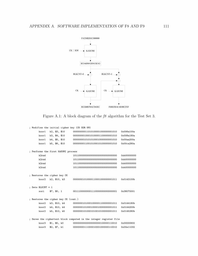
APPENDIX A. SOFTWARE IMPLEMENTATION OF F8 AND F9 111
BLKCNT=1BLKCNT=0
KASUMI KASUMI
KASUMI
FA556B261C000000
CK CK
3E5A6D0A3D1C82A5
365568B78ACD43EC F6BED6AC4E0BCD5F
CK KM
Figure A.1: A block diagram of the f8 algorithm for the Test Set 3.
; Modifies the initial cipher key (CK XOR KM)
kxor1 k2, $3, $10 00000000011010100001000000001010 0x006a100a
kxor1 k3, $4, $10 00000000100010100001100000001010 0x008a180a
kxor1 k4, $5, $10 00000000101010100010000000001010 0x00aa200a
kxor1 k5, $6, $10 00000000110010100010100000001010 0x00ca280a
; Performs the first KASUMI process
k2rnd 10110000000000000000000000000000 0xb00000000
k2rnd 10110000000000000000000000000000 0xb00000000
k2rnd 10110000000000000000000000000000 0xb00000000
k2rnd 10110000000000000000000000000000 0xb00000000
; Restores the cipher key CK
kxor2 k2, $10, k3 00000001010000110001000000001011 0x0143100b
; Sets BLKCNT = 1
xori $7, $0, 1 00111000000001110000000000000001 0x38070001
; Restores the cipher key CK (cont.)
kxor2 k3, $10, k4 00000001010001000001100000001011 0x0144180b
kxor2 k4, $10, k4 00000001010001000010000000001011 0x0144200b
kxor2 k5, $10, k5 00000001010001010010100000001011 0x0145280b
; Saves the ciphertext block computed in the integer register file
kxor3 $1, $0, k0 00000000000000000000100000110010 0x00000832
kxor3 $2, $7, k1 00000000111000010001000000110010 0x00e11032

APPENDIX A. SOFTWARE IMPLEMENTATION OF F8 AND F9 112
; Performs the second KASUMI process
k2rnd 10110000000000000000000000000000 0xb0000000
k2rnd 10110000000000000000000000000000 0xb0000000
k2rnd 10110000000000000000000000000000 0xb0000000
k2rnd 10110000000000000000000000000000 0xb0000000
; no-operations
xor $0, $0, $0 00000000000000000000000000100110 0x00000026
xor $0, $0, $0 00000000000000000000000000100110 0x00000026
xor $0, $0, $0 00000000000000000000000000100110 0x00000026
; XORs the output of the previous KASUMI process with the value BLKCNT = 1
kxor2 k0, $1, k0 00000000001000000000000000001011 0x0020000b
kxor2 k1, $2, k1 00000000010000010000100000001011 0x0041080b
; Performs the third KASUMI process
k2rnd 10110000000000000000000000000000 0xb0000000
k2rnd 10110000000000000000000000000000 0xb0000000
k2rnd 10110000000000000000000000000000 0xb0000000
k2rnd 10110000000000000000000000000000 0xb0000000
Figure A.2 illustrates a simplified timing diagram of the extended processor ex-
ecuting the previous program, captured during simulation from a VHDL waveform
analyzer. The diagram is split into four sections of 1050 ns each. The signals shown
are the inputs to the ID stage corresponding to the instruction to decode (In Instr)
and the value of the program counter (In IP), the overall clock and reset signals, and
the subregisters in the ID/EX pipeline register that provide the K1 module with a
plaintext block (l0 and r0).
The first instruction enters ID at 100 ns from start and then a new one enters
every 100 ns. The l0 and r0 registers are updated one clock cycle before registers
0 and 1 in the extended register file are due to the action of the forwarding unit.
Notice this effect at 6150 ns in figure A.2(f), where the l0 and r0 pipeline registers
hold the correct output of the last KASUMI block before it is actually written into
the extended register file, which occurs at 6250 ns.

APPENDIX A. SOFTWARE IMPLEMENTATION OF F8 AND F9 113
(a)
(b)
Fig
ure
A.2
:T
imin
gdia
gram
ofth
eex
tended
core
exec
uti
ng
apro
gram
imple
men
ting
the
test
set
3fo
rf8
.

APPENDIX A. SOFTWARE IMPLEMENTATION OF F8 AND F9 114
(c)
(d)
Fig
ure
A.2
:T
imin
gdia
gram
ofth
eex
tended
core
exec
uti
ng
apro
gram
imple
men
ting
the
test
set
3fo
rf8
.(c
ont.
)

APPENDIX A. SOFTWARE IMPLEMENTATION OF F8 AND F9 115
(e)
(f)
Fig
ure
A.2
:T
imin
gdia
gram
ofth
eex
tended
core
exec
uti
ng
apro
gram
imple
men
ting
the
test
set
3fo
rf8
.(c
ont.
)
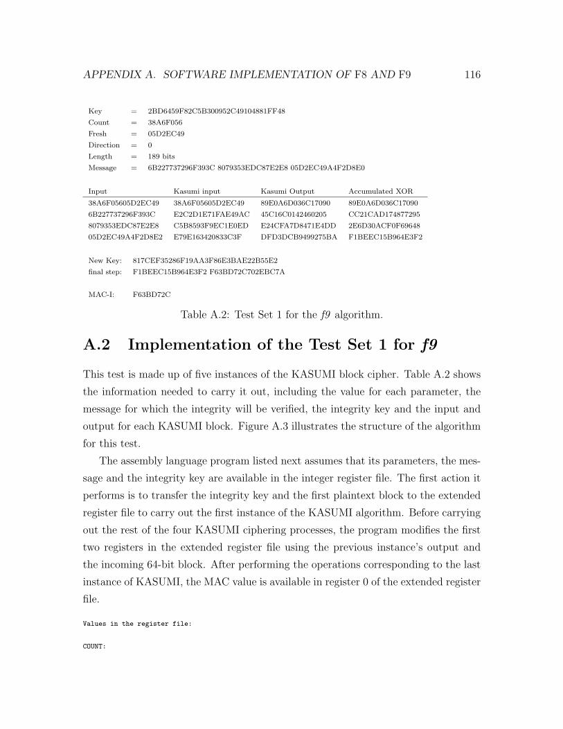
APPENDIX A. SOFTWARE IMPLEMENTATION OF F8 AND F9 116
Key = 2BD6459F82C5B300952C49104881FF48
Count = 38A6F056
Fresh = 05D2EC49
Direction = 0
Length = 189 bits
Message = 6B227737296F393C 8079353EDC87E2E8 05D2EC49A4F2D8E0
Input Kasumi input Kasumi Output Accumulated XOR
38A6F05605D2EC49 38A6F05605D2EC49 89E0A6D036C17090 89E0A6D036C17090
6B227737296F393C E2C2D1E71FAE49AC 45C16C0142460205 CC21CAD174877295
8079353EDC87E2E8 C5B8593F9EC1E0ED E24CFA7D8471E4DD 2E6D30ACF0F69648
05D2EC49A4F2D8E2 E79E163420833C3F DFD3DCB9499275BA F1BEEC15B964E3F2
New Key: 817CEF35286F19AA3F86E3BAE22B55E2
final step: F1BEEC15B964E3F2 F63BD72C702EBC7A
MAC-I: F63BD72C
Table A.2: Test Set 1 for the f9 algorithm.
A.2 Implementation of the Test Set 1 for f9
This test is made up of five instances of the KASUMI block cipher. Table A.2 shows
the information needed to carry it out, including the value for each parameter, the
message for which the integrity will be verified, the integrity key and the input and
output for each KASUMI block. Figure A.3 illustrates the structure of the algorithm
for this test.
The assembly language program listed next assumes that its parameters, the mes-
sage and the integrity key are available in the integer register file. The first action it
performs is to transfer the integrity key and the first plaintext block to the extended
register file to carry out the first instance of the KASUMI algorithm. Before carrying
out the rest of the four KASUMI ciphering processes, the program modifies the first
two registers in the extended register file using the previous instance’s output and
the incoming 64-bit block. After performing the operations corresponding to the last
instance of KASUMI, the MAC value is available in register 0 of the extended register
file.
Values in the register file:
COUNT:

APPENDIX A. SOFTWARE IMPLEMENTATION OF F8 AND F9 117
KASUMI KASUMI
KASUMI
KASUMI KASUMIIK IK IK IK
38A6F05605D2EC49 6B227737296F393C 8079353EDC87E2E8 05D2EC49A4F2D8E2
IK KM
F63BD72C702EBC7A
Figure A.3: A block diagram of the f9 algorithm for the Test Set 1.
$1 : 00111000101001101111000001010110 0x38a6f056
FRESH:
$2 : 00000101110100101110110001001001 0x05d2ec49
MESSAGE:
$3 : 01101011001000100111011100110111 0x6b227737
$4 : 00101001011011110011100100111100 0x296f393c
$5 : 10000000011110010011010100111110 0x8079353e
$6 : 11011100100001111110001011101000 0xdc87e2e8
$7 : 00000101110100101110110001001001 0x05d2ec49
$8 : 10100100111100101101100011100000 0xa4f2d8e0
IK:
$9 : 00101011110101100100010110011111 0x2bd6459f
$10 : 10000010110001011011001100000000 0x82c5b300
$11 : 10010101001011000100100100010000 0x952c4910
$12 : 01001000100000011111111101001000 0x4881ff48
Accumulator:
$13 : XXXXXXXXXXXXXXXXXXXXXXXXXXXXXXXX
$14 : XXXXXXXXXXXXXXXXXXXXXXXXXXXXXXXX
KM:
$15 : 10101010101010101010101010101010 0xaaaaaaaa
.text
; Sets the initial plaintext block to COUNT||FRESH
kxor1 k0, $1, $0 00000000001000000000000000001010 0x0020000a
kxor1 k1, $2, $0 00000000010000000000100000001010 0x0040080a

APPENDIX A. SOFTWARE IMPLEMENTATION OF F8 AND F9 118
; Sets the initial integrity key (IK)
kxor1 k2, $9, $0 00000001001000000001000000001010 0x0120100a
kxor1 k3, $10, $0 00000001010000000001100000001010 0x0140180a
kxor1 k4, $11, $0 00000001011000000010000000001010 0x0160200a
kxor1 k5, $12, $0 00000001100000000010100000001010 0x0180280a
; Performs the first KASUMI process
k2rnd 10110000000000000000000000000000 0xb0000000
k2rnd 10110000000000000000000000000000 0xb0000000
k2rnd 10110000000000000000000000000000 0xb0000000
k2rnd 10110000000000000000000000000000 0xb0000000
; no-operation
xor $0, $0, $0 00000000000000000000000000100110 0x00000026
xor $0, $0, $0 00000000000000000000000000100110 0x00000026
xor $0, $0, $0 00000000000000000000000000100110 0x00000026
; The result of the last KASUMI process is added to the accumulator
kxor3 $13, $0, k0 00000000000000000110100000110010 0x00006832
kxor3 $14, $0, k1 00000000000000010111000000110010 0x00017032
; The result of the last KASUMI process is added to the first 64-bit long block of MESSAGE
kxor2 k0, $3, k0 00000000011000000000000000001011 0x0060000b
kxor2 k1, $4, k1 00000000100000010000100000001011 0x0081080b
; Performs the second KASUMI process
k2rnd 10110000000000000000000000000000 0xb0000000
k2rnd 10110000000000000000000000000000 0xb0000000
k2rnd 10110000000000000000000000000000 0xb0000000
k2rnd 10110000000000000000000000000000 0xb0000000
; no operation
xor $0, $0, $0 00000000000000000000000000100110 0x00000026
xor $0, $0, $0 00000000000000000000000000100110 0x00000026
xor $0, $0, $0 00000000000000000000000000100110 0x00000026
; The result of the last KASUMI process is added to the accumulator
kxor3 $13, $13, k0 00000001101000000110100000110010 0x01a06832
kxor3 $14, $14, k1 00000001110000010111000000110010 0x01c17032
; The result of the last KASUMI process is added to the next 64-bit long block of MESSAGE
kxor2 k0, $5, k0 00000000101000000000000000001011 0x00a0000b
kxor2 k1, $6, k1 00000000110000010000100000001011 0x00c1080b
; Performs the third KASUMI process
k2rnd 10110000000000000000000000000000 0xb0000000
k2rnd 10110000000000000000000000000000 0xb0000000

APPENDIX A. SOFTWARE IMPLEMENTATION OF F8 AND F9 119
k2rnd 10110000000000000000000000000000 0xb0000000
k2rnd 10110000000000000000000000000000 0xb0000000
; no operation
xor $0, $0, $0 00000000000000000000000000100110 0x00000026
xor $0, $0, $0 00000000000000000000000000100110 0x00000026
xor $0, $0, $0 00000000000000000000000000100110 0x00000026
; The result of the last KASUMI process is added to the accumulator
kxor3 $13, $13, k0 00000001101000000110100000110010 0x01a06832
kxor3 $14, $14, k1 00000001110000010111000000110010 0x01c17032
; The result of the last KASUMI process is added to the next 64-bit long block of MESSAGE
kxor2 k0, $7, k0 00000000111000000000000000001011 0x00e0000b
kxor2 k1, $8, k1 00000001000000010000100000001011 0x0101080b
; Performs the fourth KASUMI process
k2rnd 10110000000000000000000000000000 0xb0000000
k2rnd 10110000000000000000000000000000 0xb0000000
k2rnd 10110000000000000000000000000000 0xb0000000
k2rnd 10110000000000000000000000000000 0xb0000000
; Modifies the integrity key
kxor2 k2, $15, k3 00000001111000110001000000001011 0x01e3100b
; no-operation
xor $0, $0, $0 00000000000000000000000000100110 0x00000026
; Modifies the integrity key (cont.)
kxor2 k3, $15, k4 00000001111001000001100000001011 0x01e4180b
kxor2 k4, $15, k4 00000001111001000010000000001011 0x01e4200b
kxor2 k5, $15, k5 00000001111001010010100000001011 0x01e5280b
; The result of the last KASUMI process is added to the next 64-bit long block of MESSAGE
kxor2 k0, $13, k0 00000001101000000000000000001011 0x01a0000b
kxor2 k1, $14, k1 00000001110000010000100000001011 0x01c1080b
; Performs the fifth KASUMI process
k2rnd 10110000000000000000000000000000 0xb0000000
k2rnd 10110000000000000000000000000000 0xb0000000
k2rnd 10110000000000000000000000000000 0xb0000000
k2rnd 10110000000000000000000000000000 0xb0000000
Figure A.4 illustrates the timing diagram of the extended core executing the pro-
gram listed previously. This diagram is longer than that in figure A.2 because it
implements five instances of the KASUMI block cipher instead of three. However,

APPENDIX A. SOFTWARE IMPLEMENTATION OF F8 AND F9 120
the two diagrams are rather similar and the conclusions mentioned for the diagram
in figure A.2 are applicable to that in figure A.4 as well. Notice that the output of
the last instance of KASUMI is ready at 10.35 µs after the start of the execution.

APPENDIX A. SOFTWARE IMPLEMENTATION OF F8 AND F9 121
(a)
(b)
Fig
ure
A.4
:T
imin
gdia
gram
ofth
eex
tended
core
exec
uti
ng
apro
gram
imple
men
ting
the
test
set
1fo
rf9
.

APPENDIX A. SOFTWARE IMPLEMENTATION OF F8 AND F9 122
(c)
(d)
Fig
ure
A.4
:T
imin
gdia
gram
ofth
eex
tended
core
exec
uti
ng
apro
gram
imple
men
ting
the
test
set
1fo
rf9
.(c
ont.
)

APPENDIX A. SOFTWARE IMPLEMENTATION OF F8 AND F9 123
(e)
(f)
Fig
ure
A.4
:T
imin
gdia
gram
ofth
eex
tended
core
exec
uti
ng
apro
gram
imple
men
ting
the
test
set
1fo
rf9
.(c
ont.
)

APPENDIX A. SOFTWARE IMPLEMENTATION OF F8 AND F9 124
(g)
(h)
Fig
ure
A.4
:T
imin
gdia
gram
ofth
eex
tended
core
exec
uti
ng
apro
gram
imple
men
ting
the
test
set
1fo
rf9
.(c
ont.
)

APPENDIX A. SOFTWARE IMPLEMENTATION OF F8 AND F9 125
(i)
(j)
Fig
ure
A.4
:T
imin
gdia
gram
ofth
eex
tended
core
exec
uti
ng
apro
gram
imple
men
ting
the
test
set
1fo
rf9
.(c
ont.
)

Appendix B
List of acronyms
1G First generation cellular communications technology
2G Second generation cellular communications technology
2.5G Advanced second generation cellular communications technology
3G Third generation cellular communications technology
3GPP Third Generation Partnership Project
AMPS Advanced Mobile Phone Services
ARIB Association of Radio Industries and Businesses
ASIC Application-Specific Integrated Circuit
ASIP Application-Specific Instruction set Processor
AuC Authentication Center
AV Authentication Vector
BRAM Block SelectRAM+
126

APPENDIX B. LIST OF ACRONYMS 127
CBC Cipher Block Chaining
CDMA Code-Division Multiple Access
CK Ciphering Key
CLB Configurable Logic Block
CN Core Network
CS Circuit-Switched
DES Data Encryption Standard
DLL Delay Lock Loop
DSP Digital Signal Processor
EDA Electronic Design Automation
EDGE Enhanced Data rates for Global Evolution
ESB Embedded System Block
ETSI European Telecommunications Standards Institute
EX Execution stage
FDD Frequency Division Duplex
FIFO First-in First-Out
FPGA Field Programmable Gate Array
FU Functional Unit

APPENDIX B. LIST OF ACRONYMS 128
GGSN Gateway GPRS Support Node
GPRS General Packet Radio Service
GRAN Generic Radio Access Network
GSM Global System for Mobile communications
HE Home Environment
HLR Home Location Register
HSCSD High-Speed Circuit-Switched Data
ID Instruction Decode stage
IF Instruction fetch stage
IK Integrity Key
IM IP-Multimedia
IMSI International Mobile Subscriber Identity
IMT-2000 International Mobile Telecommunications-2000
IOB Input/Output Block
IP a. Internet Protocol, b. Intellectual Property
ISA Instruction Set Architecture
ITU International Telecommunications Union
IV Initialization Vector
Kbps Kilobits per second

APPENDIX B. LIST OF ACRONYMS 129
KEU KASUMI Execution Unit
KM Key Modifier
LC Logic Cell
LUT Lookup Table
MAC-I Message Authentication Code for Integrity of signaling data
Mbps Megabits per second
ME Mobile Equipment
MEM Memory access stage
MIPS Microprocessor without Interlocked Pipeline Stages
MMU Memory Management Unit
MSS Mobile Satellite Service
NMT Nordic Mobile Technology
OFB Output Feedback
PCI Peripheral Component Interconnect
PDC Personal Digital Cellular
PLMN Public Land Mobile Network
PS Packet-Switched
PSTN Public Switched Telephone Networks
APPENDIX B. LIST OF ACRONYMS 130
PVN Private Virtual Network
QoS Quality of Service
RISC Reduced Instruction Set Computer
RNC Radio Network Controller
ROM Read-Only Memory
S-box Substitution box
SGSN Serving GPRS Support Node
SIM Subscriber Identity Module
SIMD Single Instruction Multiple Data
SN Serving Network
SPARC Scalable Processor Architecture
TDD Time Division Duplex
TACS Total Access Communications System
UIA UMTS Integrity Algorithm
UMTS Universal Mobile Telecommunications System
UMTS AKA UMTS Authentication and Key Agreement
USIM UMTS Subscriber Identity Module
UTRA Universal Terrestrial Radio Access

APPENDIX B. LIST OF ACRONYMS 131
UTRAN UMTS Terrestrial Radio Access Network
VHDL Very High Speed Integrated Circuit Hardware Description Language
VLIW Very Long Instruction Word
VLR Visitor Location Register
WB Write back stage
WCDMA Wideband Code-Division Multiple Access
XMAC-I Message Authentication Code for Integrity of signaling data
XST Xilinx Synthesis Technology

List of Figures
2.1 Spectrum allocation for IMT-2000 and MSS (Mobile Satellite Service)
in several countries . . . . . . . . . . . . . . . . . . . . . . . . . . . . 16
2.2 Basic architecture of a UMTS mobile network (Release 99) . . . . . . 18
2.3 Overview of the security architecture . . . . . . . . . . . . . . . . . . 21
2.4 Authentication and key agreement security mechanism . . . . . . . . 23
2.5 Derivation of message authentication codes from signaling information
using the f9 algorithm . . . . . . . . . . . . . . . . . . . . . . . . . . 25
2.6 The f9 integrity algorithm . . . . . . . . . . . . . . . . . . . . . . . . 26
2.7 Ciphering of user and signaling data using the f8 algorithm . . . . . . 27
2.8 The f8 confidentiality algorithm . . . . . . . . . . . . . . . . . . . . . 28
2.9 The KASUMI block cipher . . . . . . . . . . . . . . . . . . . . . . . . 30
2.10 The KGCORE keystream generator function . . . . . . . . . . . . . . 31
2.11 The A5/3 stream cipher . . . . . . . . . . . . . . . . . . . . . . . . . 32
2.12 The GEA3 stream cipher . . . . . . . . . . . . . . . . . . . . . . . . . 33
3.1 Single-round architectures implementing the KASUMI block cipher . 35
3.2 Two-round iterative KASUMI architecture . . . . . . . . . . . . . . . 37
3.3 Two simplified iterative KASUMI architectures . . . . . . . . . . . . 39
3.4 Two-round dual edge-triggered pipelined KASUMI architecture . . . 40
3.5 Eight-round pipelined KASUMI architecture . . . . . . . . . . . . . . 41
3.6 Eight-round dual edge-triggered pipelined KASUMI architecture . . . 42
3.7 KASUMI intellectual property core from sciworx . . . . . . . . . . . . 43
3.8 Key scheduler for the single-round pipelined architecture . . . . . . . 44
3.9 Key scheduler for simplified architectures . . . . . . . . . . . . . . . . 45
132

LIST OF FIGURES 133
3.10 Key scheduler for dual edge-triggered KASUMI architectures . . . . . 46
3.11 Iterative architectures implementing f8 and f9 . . . . . . . . . . . . . 47
3.12 Merged architecture for f8 and f9 . . . . . . . . . . . . . . . . . . . . 48
3.13 Security system for GPRS mobile stations . . . . . . . . . . . . . . . 52
3.14 Iterative GEA3 architecture . . . . . . . . . . . . . . . . . . . . . . . 53
3.15 Organization of the MPC185 security coprocessor . . . . . . . . . . . 54
5.1 Sequence of steps to design a reusable datapath for a single FO function 64
5.2 Datapath implementing two merged FI function blocks . . . . . . . . 65
5.3 Datapath for one simplified round . . . . . . . . . . . . . . . . . . . . 67
5.4 The components of the key scheduling system for the first architecture 67
5.5 Sequence of steps to design a reusable datapath for a double FO function 69
5.6 Datapath for the superFO module including a dual-port FI block . . 72
5.7 Reusable datapath implementing the operations for two rounds . . . . 73
5.8 The key scheduler module for the two-round architecture . . . . . . . 74
5.9 Pipelined datapath for the two-round sequence . . . . . . . . . . . . . 76
5.10 Pipelined key scheduler . . . . . . . . . . . . . . . . . . . . . . . . . . 78
5.11 Shift register-based key scheduler . . . . . . . . . . . . . . . . . . . . 80
5.12 Organization of a Virtex-E slice . . . . . . . . . . . . . . . . . . . . . 82
6.1 The MyRISC MIPS-based processor core with the extended KASUMI
functional unit . . . . . . . . . . . . . . . . . . . . . . . . . . . . . . 90
6.2 The organization of the extended KASUMI register file . . . . . . . . 91
6.3 Pipelined datapath for the two-round sequence . . . . . . . . . . . . . 93
6.4 Format of the kxor1 instruction . . . . . . . . . . . . . . . . . . . . . 95
6.5 Format of the kxor2 instruction . . . . . . . . . . . . . . . . . . . . . 95
6.6 Format of the kxor3 instruction . . . . . . . . . . . . . . . . . . . . . 96
6.7 Format of the k2rnd instruction . . . . . . . . . . . . . . . . . . . . . 97
6.8 Pipelined execution of a sequence of extended instructions . . . . . . 98
A.1 A block diagram of the f8 algorithm for the Test Set 3 . . . . . . . . 111
A.2 Timing diagram of the extended core executing a program implement-
ing the test set 3 for f8 . . . . . . . . . . . . . . . . . . . . . . . . . . 113

LIST OF FIGURES 134
A.3 A block diagram of the f9 algorithm for the Test Set 1 . . . . . . . . 117
A.4 Timing diagram of the extended core executing a program implement-
ing the test set 1 for f9 . . . . . . . . . . . . . . . . . . . . . . . . . . 121

List of Tables
2.1 Key scheduling for the KASUMI algorithm . . . . . . . . . . . . . . . 29
3.1 Implementation results for the two-round architecture . . . . . . . . . 37
3.2 Implementation results for the simplified architectures . . . . . . . . . 38
3.3 Implementation results for the eight-round architecture . . . . . . . . 41
3.4 Implementation results for the f8 architecture . . . . . . . . . . . . . 47
3.5 Implementation results for the f9 architecture . . . . . . . . . . . . . 48
3.6 Implementation results for the merged architecture . . . . . . . . . . 49
5.1 Summary of the synthesis results for the architectures proposed . . . 83
5.2 Summary of information concerning performance and hardware com-
plexity for the different architectures implementing the KASUMI block
cipher in FPGA technology . . . . . . . . . . . . . . . . . . . . . . . 85
6.1 Instruction analysis for the FI() function . . . . . . . . . . . . . . . . 100
6.2 Instruction analysis for the FO() function . . . . . . . . . . . . . . . . 101
6.3 Instruction analysis for the FO() function . . . . . . . . . . . . . . . . 101
6.4 Instruction analysis for the FO() function . . . . . . . . . . . . . . . . 102
6.5 Instruction analysis for the FO() function . . . . . . . . . . . . . . . . 103
6.6 Synthesis results for the components of the KASUMI functional unit 104
A.1 Test Set 3 for the f8 algorithm . . . . . . . . . . . . . . . . . . . . . . 110
A.2 Test Set 1 for the f9 algorithm . . . . . . . . . . . . . . . . . . . . . . 116
135

Bibliography
[1] 3rd Generation Partnership Program, Network Architecture, Technical Specifi-
cation 23.002, Release 5, Version 5.5.0, 2002.
[2] 3rd Generation Partnership Program, Security Architecture, Technical Specifica-
tion 33.102, Release 5, Version 5.2.0, 2003.
[3] 3rd Generation Partnership Program, Cryptographic Algorithm Requirements ,
Technical Specification 33.105, Release 4, Version 4.1.0, 2001.
[4] 3rd Generation Partnership Program, Specification of the 3GPP Confidentiality
and Integrity Algorithms; Document 1: f8 and f9 Specification, Technical Speci-
fication 35.201, Release 5, Version 5.0.0, 2002.
[5] 3rd Generation Partnership Program, Specification of the 3GPP Confidentiality
and Integrity Algorithms; Document 2: KASUMI Specification, Technical Spec-
ification 35.202, Release 5, Version 5.0.0, 2002.
[6] 3rd Generation Partnership Program, Specification of the 3GPP Confidential-
ity and Integrity Algorithms; Document 3: Implementors’ Test Data, Technical
Specification 35.203, Release 5, Version 5.0.0, 2002.
[7] 3rd Generation Partnership Program, Security Related Network Functions , Tech-
nical Specification 43.020, Release 6, Version 6.0.0, 2004.
[8] 3rd Generation Partnership Program, Specification of the A5/3 Encryption Al-
gorithms for GSM and ESCD, and the GEA3 Encryption Algorithm for GPRS;
Document 1: A5/3 and GEA3 Specifications , Technical Specification 55.216,
Release 6, Version 6.2.0, 2003.
136

BIBLIOGRAPHY 137
[9] T. Balderas and R. Cumplido, Security Architecture in UMTS Third Genera-
tion Cellular Networks , Technical Report CCC-04-002, Computer Science De-
partment, Instituto Nacional de Astrofısica, Optica y Electronica, Tonantzintla,
Puebla, Mexico.
[10] T. Balderas and R. Cumplido, “An Efficient Reuse-Based Approach to Imple-
ment the 3GPP KASUMI Block Cipher”, in Proc. of the First International
Conference on Electrical and Electronics Engineering and Tenth Conference on
Electrical Engineering ICEEE/CIE , CINVESTAV-IPN, Acapulco, Mexico, 2004,
pp. 113–118.
[11] T. Balderas and R. Cumplido, “An Efficient Hardware Implementation of the
KASUMI Block Cipher for Third Generation Cellular Networks”, in Proc. of the
Global Signal Processing Conference GSPx 2004 , Santa Clara, CA, 2004.
[12] T. Balderas and R. Cumplido, “An Efficient FPGA Architecture for Block Ci-
phering in Third Generation Cellular Networks”, in Research on Computer Sci-
ence Vol. 10, Advances in: Artificial Intelligence, Computing Science and Com-
puter Engineering , CIC-IPN, ISBN:970-36-0194-4, Mexico, 2004.
[13] A. Biryukov, A. Shamir and D. Wagner,“Real Time Cryptanalysis of A5/1 on
a PC”, in Proc. of the 7th International Workshop on Fast Software Encryption
FSE 2000 , New York, NY, 2000, pp. 1–18.
[14] P. Chodowiec, P. Khuon and K. Gaj, “Fast Implementation of Secret-Key
Block Cipher Using Mixed Inner- and Outer-Round Pipelining”, in Proc. of the
ACM/SIGDA 9th International Symposium on Field Programmable Gate Arrays
FPGA 2001 , Monterey, CA, 2001, pp. 94–102.
[15] P. Davies and S. Robsky, Accelerating Network Processing with Extensions to the
User-Customizable ARCtangentTM Microprocessor. Case Study #1: Accelerating
DES Cryptography , 2002.
[16] M. Dworkin, Recommendation for Block Cipher Modes of Operation, NIST Spe-
cial Publication 800-38A, 2001.

BIBLIOGRAPHY 138
[17] M. Gschwind, “Instruction Set Selection for ASIP Design”, in Proc. of the 7th
International Workshop on Hardware/Software Co-Design CODES’99 , Rome,
Italy, 1999, pp. 7–11.
[18] J. L. Hennessy, and D. A. Patterson, Computer Organization and Design. The
Hardware/Software Interface, Morgan Kaufmann Publishers, Inc., San Francisco,
CA., 1998.
[19] International Telecommunications Union, International Mobile
Telecommunications-2000 , Recommendation ITU-R M.687-2 (02/97), 1997.
[20] H. Kim, Y. Choi, M. Kim and H. Ryu, “Hardware Implementation of the 3GPP
KASUMI Crypto Algorithm”, in Proc. of the 2002 International Technical Con-
ference on Circuits/Systems, Computers and Communications ITC-CSCC-2002 ,
Phuket, Thailand, 2002, pp. 317–320.
[21] P. Kitsos, M. D. Galanis and O. Koufopavlou, “High-Speed Hardware Implemen-
tations of the KASUMI Block Cipher”, in Proc. of the 2004 IEEE International
Symposium on Circuit and Systems ISCAS’04 , Vancouver, Canada, 2004.
[22] P. Kitsos, N. Sklavos, and O. Koufopavlou, “An End-to-End Hardware Approach
Security for the GPRS”,in Proc. of the 12th IEEE Mediterranean Electrotechnical
Conference MELECON 2004 , Dubrovnik, Croatia, 2004.
[23] J. Korhonen, Introduction to 3G Mobile Communications , Artech House, Inc.,
Norwood, MA., 2001.
[24] K. Marinis, N. K. Moshopoulos, F. Karoubalis and K. Z. Pekmestzi, “On
the Hardware Implementation of the 3GPP Confidentiality and Integrity Al-
gorithms”, in Proc. of the 4th International Conference on Information Security
ISC 2001 , Malaga, Spain, LNCS 2200/2001, Springer-Verlag, 2001, pp. 248–265.
[25] M. Matsui, “New Block Encryption Algorithm MISTY”, in Proc. of the 4th
International Fast Software Encryption Workshop FSE’97 , Haifa, Israel, LNCS
1267/1997, Springer-Verlag, 1997, pp. 54–68.

BIBLIOGRAPHY 139
[26] MIPS Technologies, MIPS SDE 5.03 Programmer’s Guide, Document Number
MD00310, Revision 1.67, 2004.
[27] Motorola, Inc., MPC185 Security Co-Processor User’s Manual , MPC185UM,
Revision 2.2, 2003.
[28] S. M. Redl, M. K. Weber and M. W. Oliphant, An Introduction to GSM , Artech
House, Inc., Norwood, MA., 1995.
[29] A. Satoh and S. Morioka, “Small and High-Speed Hardware Architectures for
the 3GPP Standard Cipher KASUMI”, in Proc. of the 5th International Con-
ference on Information Security ISC 2002 , Sao Paulo, Brazil, LNCS 2433/2002,
Springer-Verlag, 2002, pp. 48–62.
[30] Sci-worx GmbH, KASUMI DesignObjectTM. Document VC01C2.009, Revision
01.00.01, 2002.
[31] C. Smith, and D. Collins, 3G Wireless Networks , McGraw-Hill, Boston, MA.,
2002.
[32] Trillium Digital Systems, Inc., Third Generation (3G) Whitepaper , Los Angeles,
CA., 2000.
http://www.trillium.com/assets/wireless3g/white paper/8722019.pdf
[33] N. Valtteri and K. Nyberg, UMTS Security , John Wiley & Sons, Ltd, England,
2003.
[34] A. Wallander, A VHDL Implementation of a MIPS , Project Report, Department
of Computer Science and Electrical Engineering, Lulea Tekniska Universitet,
Lulea, Sweden.
[35] Xilinx, Inc., Virtex-E 1.8 V Field Programmable Gate Arrays. v2.6. Product
Specification, 2002.
[36] Xilinx, Inc., XST User Guide, 2003.