Hardware User Guide - docs-apac.rs-online.com · The Flash evaluation board supports three Flash...
20
AT89STK-10 Starter Kit ............................................................................................. Hardware User Guide
Transcript of Hardware User Guide - docs-apac.rs-online.com · The Flash evaluation board supports three Flash...

AT89STK-10 Starter Kit ..............................................................................................
Hardware User Guide

AT89STK-10 Starter Kit Hardware
Section 1Introduction ........................................................................................... 1-2
1.1 Features....................................................................................................1-2
Section 2Hardware Description ......................................................................... 2-10Typical Applications ............................................................................ 2-11
3.1 Nand Flash Application ...........................................................................2-123.2 Serial Dataflash Application ....................................................................2-13
Section 3Annex.................................................................................................. 3-14
4.1 Flash Evaluation Board...........................................................................3-154.2 Nand Flash Add-on board .......................................................................3-18
User User Guide 1
7534A–USB–07/05

Section 1
Introduction
This document describes the Flash Evaluation Board dedicated to the AT89C5130/31Aand the AT8xC5122D USB microcontrollers. This board is designed to enable an easyevaluation of the Mass Storage USB class using demonstration firmware (refer to firm-ware Guide). It must be plugged to a CPU board (AT89C5130/31A or AT8xC5122 Devaluation board).
1.1 Features The Flash evaluation board provides the following features:
Support the following microcontrollers :
– AT89C5130A
– AT89C5131A
– AT8xC5122D
No external power supply required
– Power supplied by the USB line via the CPU board (AT89C5130/31A orAT8xC5122 D evaluation board)
On board DataFlash memory (ATMEL AT45DB321B, 4MB)
Support Nand Flash memory (MICRON MT29F2GO8AABWP, 256MB) - Add-on board
Support Pluggable DataFlash Card (ATMEL AT45DCB004C, 4 MB)
AT89STK-10 Starter Kit Hardware User Guide 1-1
Rev. 7534A–USB–07/05

Figure 1-1. Flash Evaluation Board
Figure 1-2. Flash Evaluation Board with the related memories
AT89STK-10 Starter Kit Hardware User Guide 1-2
Rev. 7534A–USB–07/05
Hardware Description
Section 2
Hardware Description
2.1 CPU board selection
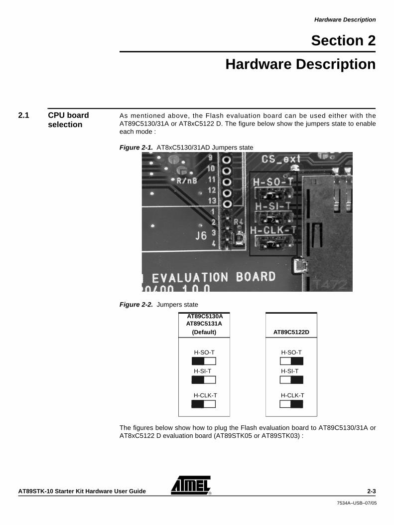
As mentioned above, the Flash evaluation board can be used either with theAT89C5130/31A or AT8xC5122 D. The figure below show the jumpers state to enableeach mode :
Figure 2-1. AT8xC5130/31AD Jumpers state
Figure 2-2. Jumpers state
The figures below show how to plug the Flash evaluation board to AT89C5130/31A orAT8xC5122 D evaluation board (AT89STK05 or AT89STK03) :
AT89C5130AAT89C5131A
(Default) AT89C5122D
H-SO-T
H-SI-T
H-CLK-T
H-SO-T
H-SI-T
H-CLK-T
AT89STK-10 Starter Kit Hardware User Guide 2-3
7534A–USB–07/05

Figure 2-3. Flash evaluation board plugged to AT89C5130/31A evaluation board(AT89STK05)
Warning : Before plugging the Flash Evoluation Board (AT89STK10) to theAT89C5130/31A evaluation board (AT89STK05), disconnect the three LEDs by remov-ing the solder on solder straps. The figure below shows the location of these solderstraps :
Figure 2-4. AT89STK-05 - LEDs Disconnection
AT89STK-10 Starter Kit Hardware User Guide 2-4
Rev. 7534A–USB–07/05

Hardware Description
Figure 2-5. Flash evaluation board plugged to AT8xC5122D evaluation board(AT89STK03)
2.2 Power supply The Flash Evaluation Board power is supplied by the CPU board. The power supply must be setto 3.3V for the AT89C5131A Evaluation board and 3.6V for the AT8xC5122D Evaluation board.The figure 2.5 shows the different possible configurations of the AT89C5130/31A Evaluationboard (AT89STK05) and the figure 2.6 shows how to select 3.6V on the AT8xC5122DEvaluation board in the 3.6V power supply configuration :
Figure 2-6. Power supply (3.3V) - AT89C5131A Evaluation Board (AT89STK05)
LIM
REG
VB
US
5V
3.3V
ICC
PWR.S.
PWR
VCC
LIM
REG
VB
US
5V
3.3V
ICC
PWR.S.
PWR
VCC
LIM
REG
VB
US
5V
3.3V
ICC
PWR.S.
PWR
VCC
LIM
REG
VB
US
5V
3.3V
ICC
PWR.S.
PWR
VCC
LIM
REG
VB
US
5V
3.3V
ICC
PWR.S.
PWR
VCC
LIM
REG
VB
US
5V
3.3V
ICC
PWR.S.
PWR
VCC
VBUS VBUS andCurrent Limiter
External
Direct Input
3.3V Regulate
PowerSource
Regulation
AT89STK-10 Starter Kit Hardware User Guide 2-5
7534A–USB–07/05

Hardware Description
Figure 2-7. Power supply (3.6V)- AT8xC5122 D Evaluation Board (AT89STK03)
2.3 Memory selection
The Flash evaluation board supports three Flash memories (Pluggable Nand Flash,Pluggable DataFlash Card and On board DataFlash). Just one memory can be acti-vated at the same time.
To configure the board with your specific usage, you have to put the solder straps in theright state.
Figure 2-8. Solder straps
Figure 2-9. Solder Straps location
The tables hereunder show the configuration related to each memory mode :
Solder location
“Open” “Close”
SP12SP11
SP13 SP14
SP9
SP10
SP1
SP5
SP7
SP3
SP15
SP2
SP6
SP4
SP8
2-6 AT89STK-10 Starter Kit Hardware User Guide
7534A–USB–07/05

Hardware Description
Table 1. Nand Flash Configuration (Default configuration)
Table 2. On Board DataFlash Configuration (Serial mode)
Table 3. On Board DataFlash Configuration (Parallel mode)
The firmware doesn’t support this mode.
Reference Name Function State
SP1..8 D0..7 Connect Data P0 on onboard dataflash Open
SP9 CS Connect CS of internal dataflash Open
SP10 R/nB Connect R/nB on dataflash Open
SP 11 SER Select DataFlash in serial mode Open
SP12 PAR Select DataFlash in parallel mode Open
SP 13 VccPConnect power supply of parallel interface of DataFlash
Open
SP 14 GNDPConnect ground of parallel interface of DataFlash
Open
SP 15 CS_ext Connect CS of external dataflash Open
Reference Name Function State
SP1..8 D0..7 Connect bus P0 on onboard dataflash Open
SP9 CS Connect CS of internal dataflash Close
SP10 R/nB Connect R/nB on dataflash Close/Open
SP 11 SER Select DataFlash in serial mode Close
SP12 PAR Select DataFlash in parallel mode Open
SP 13 VccPconnect power supply of parallel interface of DataFlash
Open
SP 14 GNDPconnect gnd of parallel interface of DataFlash
Open
SP 15 CS_ext Connect CS of external dataflash Open
Reference Name Function State
SP1..8 D0..7 connect bus P0 on onboard dataflash Close
SP9 CS Connect CS of internal dataflash Close
SP10 R/nB Connect R/nB on dataflash Close
SP 11 SER put DataFlash in serial mode Open
SP12 PAR put DataFlash in parallel mode Close
SP 13 VccPconnect power supply of parallel interface of DataFlash
Close
SP 14 GNDPconnect gnd of parallel interface of DataFlash
Close
SP 15 CS_ext Connect CS of external dataflash Open
AT89STK-10 Starter Kit Hardware User Guide 2-7
7534A–USB–07/05

Hardware Description
Table 4. Pluggable DataFlash Card Configuration
Reference Name Function State
SP1..8 D0..7 connect bus P0 on onboard dataflash Open
SP9 CS Connect CS of internal dataflash Open
SP10 R/nB Connect R/nB on dataflash Open
SP 11 SER put DataFlash in serial mode Open
SP12 PAR put DataFlash in parallel mode Open
SP 13 VccPconnect power supply of parallel interface of DataFlash
Open
SP 14 GNDPconnect gnd of parallel interface of DataFlash
Open
SP 15 CS_ext Connect CS of external dataflash Close
2-8 AT89STK-10 Starter Kit Hardware User Guide
7534A–USB–07/05

Typical Applications
Section 3
Typical Applications
AT89STK-10 Starter Kit Hardware User Guide 3-9
7534A–USB–07/05

Typical Applications
3.1 Nand Flash Application
P0.0
P0.1
P0.2
P0.3
P0.4
P0.5
P0.6
P0.7
AVss Vss
Xtal2
Xtal124
MHz
22pF
22pF
100
27
27
1.5k
D-
D+
Vref
PLLF10nF 2.2nF
I/O.0
I/O.1
I/O.2
I/O.3
I/O.4
I/O.5
I/O.6
I/O.7
Nand Flash
AT89C5131A-M
Vss
P2.0
P2.1
CLE
ALE
USB connector
3.3Vregulator
D-
D+
Vbus
GND
2.2k
Vcc
Vcc
R/B
10µFTantal.
P3.7
P2.3
P2.4
VDD AVDD
1µF
100nF
Vcc
P3.3
Vcc
EA
100k
P3.0
WriteProtection
2.2k
WE
CE
RE
P3.6
PSEN
ISP
2.2k
optional
10µFTantal.
10k
Vcc
WP
Ucap
3-10 AT89STK-10 Starter Kit Hardware User Guide
7534A–USB–07/05

3.2 Serial Dataflash Application
P0.0
P0.1
P0.2
P0.3
P0.4
P0.5
P0.6
P0.7
AVss Vss
Xtal2
Xtal124
MHz
22pF
22pF
100
27
27
1.5k
D-
D+
Vref
PLLF10nF 2.2nF
Data FlashAT45DB321B
AT89C5131A-M
Vss
P2.3
P1.6
CS
SCK/CLK
USB connector
3.3Vregulator
D-
D+
Vbus
GND
Vcc
RDY/BUSY
10µFTantal.
P1.7/MOSI
P1.5/MISO
P2.4
VDD AVDD
1µF
100nF
Vcc
P3.3
Vcc
EA
100k
P3.0
WriteProtection
2.2k
SI
PSEN
ISP
2.2k
optional
10µFTantal.
10k
Vcc
Reset
Ucap
10k
Vcc
WP
SO
SER/PAR
Vcc
AT89STK-10 Starter Kit Hardware User Guide 3-11
Rev. 7534A–USB–07/05

Annex
Section 4
Annex
4-12 AT89STK-10 Starter Kit Hardware User Guide
7534A–USB–07/05

Annex
4.1 Flash Evaluation Board
NF_nWE
NF_nWP0
NF_nWP2
NF_nRE
Vcc
NF_nCE1
NF_CLENF_ALENF_R/nB1
NF_R/nB0NF_nCE0
NF_D7
NF_D5NF_D4
NF_D6
NF_D3NF_D2NF_D1NF_D0
NF_nWP3
NF_nWP1
Vcc
R/nB1
nCE1
CLEALE
nCE0R/nB0
nREnWE
P0_0P0_1P0_2P0_3P0_4P0_5P0_6P0_7
Vss
P2_6P2_7C51_ALERESET
SICLK
SOSER/nPAR
Vcc
nWP
nWP nWP
nWP
1
32
4
HE13 _4 FD
J5
HE13 _4 FD
J5
1
3
5
2
4
6789
10111213
HE13 _13 FD
J4
HE13 _13 FD
J41
3
5
2
4
678910111213
HE13 _13 FD
J3
HE13 _13 FD
J3
1
32
4
HE13 _4 FD
J6
HE13 _4 FD
J6
R410 KR410 K
AT89STK-10 Starter Kit Hardware User Guide 4-13
7534A–USB–07/05

Annex
P1_7P1_6P1_5
_WE_RE
VssVss
Vcc_CPUVss
Vss
Vss
Vss
Vss
VssVss
P0_0P0_1P0_2P0_3P0_4P0_5P0_6P0_7P2_0P2_1P2_2P2_3P2_4P2_5
P4_0P4_1P4_2
C51_ALEP2_6P2_7
MISO_TCLK_TMOSI_T
nRE
VssVss
VccVss
Vss
Vss Vss
VssVss
Vss
MISO_HMOSI_H
P0_0P0_1P0_2P0_3P0_4P0_5P0_6P0_7CLEALER/nB1nCE0R/nB0nCE1
CLK_H
C51_ALEnWE
CLE ALE R/nB1 nCE0 R/nB0 nCE1 Vss
P2_6P2_7
1
TP9TP9
1
TP8TP8
24681012141618202224262830323436384042444648
13579
11131517192123252729313335373941434547
J2
HEADER 24X2
flashbord Right
J2
HEADER 24X2
flashbord Right
1TP7TP7
1
TP6TP6
1
TP5TP5
1
TP4TP4
1
TP10TP10
24681012141618202224262830323436384042444648
13579
11131517192123252729313335373941434547
J1
HEADER 24X2
flashboard Left
J1
HEADER 24X2
flashboard LeftFlash Board RightFlash Board Left
4-14 AT89STK-10 Starter Kit Hardware User Guide
7534A–USB–07/05

Annex
AT89STK-10 Starter Kit Hardware User Guide 4-15
7534A–USB–07/05

Annex
4.2 Nand Flash Add-on board
Figure 4-1. Schematic
4-16 AT89STK-10 Starter Kit Hardware User Guide
7534A–USB–07/05

Annex
Figure 4-2. Component Side
Figure 4-3. Solder Side
AT89STK-10 Starter Kit Hardware User Guide 4-17
7534A–USB–07/05

Printed on recycled paper.
Disclaimer: The information in this document is provided in connection with Atmel products. No license, express or implied, by estoppel or otherwise, to anyintellectual property right is granted by this document or in connection with the sale of Atmel products. EXCEPT AS SET FORTH IN ATMEL’S TERMS AND CONDI-TIONS OF SALE LOCATED ON ATMEL’S WEB SITE, ATMEL ASSUMES NO LIABILITY WHATSOEVER AND DISCLAIMS ANY EXPRESS, IMPLIED OR STATUTORYWARRANTY RELATING TO ITS PRODUCTS INCLUDING, BUT NOT LIMITED TO, THE IMPLIED WARRANTY OF MERCHANTABILITY, FITNESS FOR A PARTICULARPURPOSE, OR NON-INFRINGEMENT. IN NO EVENT SHALL ATMEL BE LIABLE FOR ANY DIRECT, INDIRECT, CONSEQUENTIAL, PUNITIVE, SPECIAL OR INCIDEN-TAL DAMAGES (INCLUDING, WITHOUT LIMITATION, DAMAGES FOR LOSS OF PROFITS, BUSINESS INTERRUPTION, OR LOSS OF INFORMATION) ARISING OUTOF THE USE OR INABILITY TO USE THIS DOCUMENT, EVEN IF ATMEL HAS BEEN ADVISED OF THE POSSIBILITY OF SUCH DAMAGES. Atmel makes norepresentations or warranties with respect to the accuracy or completeness of the contents of this document and reserves the right to make changes to specificationsand product descriptions at any time without notice. Atmel does not make any commitment to update the information contained herein. Unless specifically providedot-herwise, Atmel products are not suitable for, and shall not be used in, automotive applications. Atmel’sAtmel’s products are not intended, authorized, or warranted for use ascomponents in applications intended to support or sustain life.
Atmel Corporation Atmel Operations
2325 Orchard ParkwaySan Jose, CA 95131Tel: 1(408) 441-0311Fax: 1(408) 487-2600
Regional Headquarters
EuropeAtmel SarlRoute des Arsenaux 41Case Postale 80CH-1705 FribourgSwitzerlandTel: (41) 26-426-5555Fax: (41) 26-426-5500
AsiaRoom 1219Chinachem Golden Plaza77 Mody Road TsimshatsuiEast KowloonHong KongTel: (852) 2721-9778Fax: (852) 2722-1369
Japan9F, Tonetsu Shinkawa Bldg.1-24-8 ShinkawaChuo-ku, Tokyo 104-0033JapanTel: (81) 3-3523-3551Fax: (81) 3-3523-7581
Memory2325 Orchard ParkwaySan Jose, CA 95131Tel: 1(408) 441-0311Fax: 1(408) 436-4314
Microcontrollers2325 Orchard ParkwaySan Jose, CA 95131Tel: 1(408) 441-0311Fax: 1(408) 436-4314
La ChantrerieBP 7060244306 Nantes Cedex 3, FranceTel: (33) 2-40-18-18-18Fax: (33) 2-40-18-19-60
ASIC/ASSP/Smart CardsZone Industrielle13106 Rousset Cedex, FranceTel: (33) 4-42-53-60-00Fax: (33) 4-42-53-60-01
1150 East Cheyenne Mtn. Blvd.Colorado Springs, CO 80906Tel: 1(719) 576-3300Fax: 1(719) 540-1759
Scottish Enterprise Technology ParkMaxwell BuildingEast Kilbride G75 0QR, Scotland Tel: (44) 1355-803-000Fax: (44) 1355-242-743
RF/AutomotiveTheresienstrasse 2Postfach 353574025 Heilbronn, GermanyTel: (49) 71-31-67-0Fax: (49) 71-31-67-2340
1150 East Cheyenne Mtn. Blvd.Colorado Springs, CO 80906Tel: 1(719) 576-3300Fax: 1(719) 540-1759
Biometrics/Imaging/Hi-Rel MPU/High Speed Converters/RF Datacom
Avenue de RochepleineBP 12338521 Saint-Egreve Cedex, FranceTel: (33) 4-76-58-30-00Fax: (33) 4-76-58-34-80
Web Sitehttp://www.atmel.com
7534A–USB–07/05 /xM
© Atmel Corporation 2005. All rights reserved. Atmel®, logo and combinations thereof, are registered trademarks, and Everywhere You Are®
are the trademarks of Atmel Corporation or its subsidiaries. Other terms and product names may be trademarks of others.

![docs-apac.rs-online.com · RL78 • 12 Device Memory Interfaces Timers & other peripherals Miscellaneous Information Core Nickname Part Number Size [KB] RAM [Byte] I/O/Pins CSI/ UARTs](https://static.fdocuments.in/doc/165x107/5f9cda2e4041a119c3535b59/docs-apacrs-rl78-a-12-device-memory-interfaces-timers-other-peripherals.jpg)