
Hardware Trust and Assurance through Reverse Engineering
54
XXX Hardware Trust and Assurance through Reverse Engineering: A Tutorial and Outlook from Image Analysis and Machine Learning Perspectives ULBERT J. BOTERO ∗ , 1 RONALD WILSON ∗ , 1 HANGWEI LU, 1 MIR TANJIDUR RAHMAN, 1 MUKHIL A. MALLAIYAN, 1 FATEMEH GANJI † , 2 NAVID ASADIZANJANI, 1 MARK M. TEHRANIPOOR, 1 DAMON L. WOODARD, 1 DOMENIC FORTE, 1 , 1 Florida Institute for Cybersecurity Research, University of Florida, and 2 Worcester Polytechnic Institute In the context of hardware trust and assurance, reverse engineering has been often considered as an illegal action. Generally speaking, reverse engineering aims to retrieve information from a product, i.e., integrated circuits (ICs) and printed circuit boards (PCBs) in hardware security-related scenarios, in the hope of un- derstanding the functionality of the device and determining its constituent components. Hence, it can raise serious issues concerning Intellectual Property (IP) infringement, the (in)effectiveness of security-related measures, and even new opportunities for injecting hardware Trojans. Ironically, reverse engineering can enable IP owners to verify and validate the design. Nevertheless, this cannot be achieved without overcoming numerous obstacles that limit successful outcomes of the reverse engineering process. This paper surveys these challenges from two complementary perspectives: image processing and machine learning. These two fields of study form a firm basis for the enhancement of efficiency and accuracy of reverse engineering processes for both PCBs and ICs. In summary, therefore, this paper presents a roadmap indicating clearly the actions to be taken to fulfill hardware trust and assurance objectives. CCS Concepts: • Security and privacy → Malicious design modifications; Hardware reverse engineer- ing. ∗ Ulbert J. Botero and Ronald Wilson contributed equally to this research. † Corresponding author. Fatemeh Ganji was with Florida Institute for Cybersecurity Research, University of Florida, when this study has been done. Authors’ addresses: Ulbert J. Botero, jbot2016@ufl.edu 1 ; Ronald Wilson, ronaldwilson@ufl.edu 1 ; Hangwei Lu, qslvhw@ ufl.edu 1 ; Mir Tanjidur Rahman, mir.rahman@ufl.edu 1 ; Mukhil A. Mallaiyan, mukhil.mallaiyan@ufl.edu 1 ; Fatemeh Ganji, [email protected] 2 ; Navid Asadizanjani, [email protected]fl.edu 1 ; Mark M. Tehranipoor, [email protected]fl.edu 1 ; Damon L. Woodard, [email protected]fl.edu 1 ; Domenic Forte, [email protected]fl.edu 1 , 1 Florida Institute for Cybersecurity Research, University of Florida, 601 Gale Lemerand Dr, Gainesville, FL, 32611, 2 Worcester Polytechnic Institute, 100 Institute Road, Worcester, MA, 01609-2280. Permission to make digital or hard copies of all or part of this work for personal or classroom use is granted without fee provided that copies are not made or distributed for profit or commercial advantage and that copies bear this notice and the full citation on the first page. Copyrights for components of this work owned by others than ACM must be honored. Abstracting with credit is permitted. To copy otherwise, or republish, to post on servers or to redistribute to lists, requires prior specific permission and/or a fee. Request permissions from [email protected]. © 2020 Association for Computing Machinery. XXXX-XXXX/2020/10-ARTXXX $15.00 https://doi.org/XXX , Vol. XX, No. X, Article XXX. Publication date: October 2020.
Transcript of Hardware Trust and Assurance through Reverse Engineering

XXX
Hardware Trust and Assurance through ReverseEngineering:A Tutorial and Outlook from Image Analysis and Machine Learning Perspectives
ULBERT J. BOTERO∗, 1
RONALD WILSON∗, 1
HANGWEI LU, 1
MIR TANJIDUR RAHMAN, 1
MUKHIL A. MALLAIYAN, 1
FATEMEH GANJI†, 2
NAVID ASADIZANJANI, 1
MARK M. TEHRANIPOOR, 1
DAMON L. WOODARD, 1
DOMENIC FORTE, 1,1 Florida Institute for Cybersecurity Research, University of Florida, and 2 Worcester Polytechnic Institute
In the context of hardware trust and assurance, reverse engineering has been often considered as an illegalaction. Generally speaking, reverse engineering aims to retrieve information from a product, i.e., integratedcircuits (ICs) and printed circuit boards (PCBs) in hardware security-related scenarios, in the hope of un-derstanding the functionality of the device and determining its constituent components. Hence, it can raiseserious issues concerning Intellectual Property (IP) infringement, the (in)effectiveness of security-relatedmeasures, and even new opportunities for injecting hardware Trojans. Ironically, reverse engineering canenable IP owners to verify and validate the design. Nevertheless, this cannot be achieved without overcomingnumerous obstacles that limit successful outcomes of the reverse engineering process. This paper surveys thesechallenges from two complementary perspectives: image processing and machine learning. These two fieldsof study form a firm basis for the enhancement of efficiency and accuracy of reverse engineering processes forboth PCBs and ICs. In summary, therefore, this paper presents a roadmap indicating clearly the actions to betaken to fulfill hardware trust and assurance objectives.
CCS Concepts: • Security and privacy→Malicious designmodifications;Hardware reverse engineer-ing.
∗Ulbert J. Botero and Ronald Wilson contributed equally to this research.†Corresponding author. Fatemeh Ganji was with Florida Institute for Cybersecurity Research, University of Florida, whenthis study has been done.
Authors’ addresses: Ulbert J. Botero, [email protected]; Ronald Wilson, [email protected]; Hangwei Lu, [email protected]; Mir Tanjidur Rahman, [email protected]; Mukhil A. Mallaiyan, [email protected]; Fatemeh Ganji,[email protected]; Navid Asadizanjani, [email protected]; Mark M. Tehranipoor, [email protected]; Damon L.Woodard, [email protected]; Domenic Forte, [email protected],1 Florida Institute for Cybersecurity Research, University of Florida, 601 Gale Lemerand Dr, Gainesville, FL, 32611, 2Worcester Polytechnic Institute, 100 Institute Road, Worcester, MA, 01609-2280.
Permission to make digital or hard copies of all or part of this work for personal or classroom use is granted without feeprovided that copies are not made or distributed for profit or commercial advantage and that copies bear this notice andthe full citation on the first page. Copyrights for components of this work owned by others than ACM must be honored.Abstracting with credit is permitted. To copy otherwise, or republish, to post on servers or to redistribute to lists, requiresprior specific permission and/or a fee. Request permissions from [email protected].© 2020 Association for Computing Machinery.XXXX-XXXX/2020/10-ARTXXX $15.00https://doi.org/XXX
, Vol. XX, No. X, Article XXX. Publication date: October 2020.

XXX:2 Botero, Wilson, et al.
Additional Key Words and Phrases: Hardware Counterfeiting, Hardware Trojan, Imaging, Image Processing,Integrated Circuits, Machine Learning, Printed Circuit Boards, Reverse Engineering, Trust and Assurance.
ACM Reference Format:Ulbert J. Botero, Ronald Wilson, Hangwei Lu, Mir Tanjidur Rahman, Mukhil A. Mallaiyan, Fatemeh Ganji,Navid Asadizanjani, Mark M. Tehranipoor, Damon L. Woodard, and Domenic Forte. 2020. Hardware Trustand Assurance through Reverse Engineering: : A Tutorial and Outlook from Image Analysis and MachineLearning Perspectives. XX, X, Article XXX (October 2020), 54 pages. https://doi.org/XXX
1 INTRODUCTIONOutsourcing of integrated circuit (IC) and printed circuit board (PCB) design, fabrication, packaging,and testing has dramatically reduced product development time and cost. In doing so, this hasenabled the widespread availability of microelectronics, which has indeed transformed modern life.However, unintended consequences include malicious design alteration (i.e., hardware Trojan inser-tion [136, 160]) and the rise of the counterfeit electronics industry [187]. Reverse engineering (RE)is widely applied for educational purposes and for detecting Intellectual Property (IP) infringement,but it can play an even more significant role in hardware trust and assurance. RE of electronic chipsand systems refers to the process of retrieving an electronic design layout and/or netlist, storedinformation (memory contents, firmware, software, etc.), and functionality/specification throughelectrical testing and/or physical inspection. Although RE is often presented in a negative light (e.g.,illegal cloning designs and/or disclosing sensitive information to a competitor or adversary), it issometimes the only foolproof way to detect malicious alteration and/or tampering by semiconductorfoundries, find vulnerabilities present in commercial-off-the-shelf (COTS) chips and avoid them,and replace obsolete (i.e., no longer manufactured) hardware.As for attaining trust and assurance, existing techniques are limited and/or ineffective. For
example, run-time monitoring techniques increase the resource requirements – power consumption,memory utilization, and area overhead on ICs/PCBs – due to on-chip/board sensors used to detectanomalous activities. In test time methods, the challenge is to generate test vectors that triggerstealthy, well-placed hardware Trojans in billion-transistor chips. Similarly, in side-channel signalanalysis approaches, inescapable process variations, and the measurement noise undermine theprobability of detecting small Trojans [89]. As a result, the confidence level in detecting Trojansusing the aforementioned techniques is quite low [28, 138, 186]. Hence, RE has been gaining moreattention in recent years and experiencing community-wide acceptance as an effective approach,in particular, for hardware Trojan detection [12, 45].In the area of IC counterfeit detection and avoidance, the current best practice requires the
use of either classification by subject matter experts (SME), procuring lifetime buys for long-termsystem maintenance, or acquiring components from untrusted distributors in a supply chain, whichpotentially involves grey market distributors. Each of these options is non-ideal. The large quantitiesof components that SME counterfeit analysts are required to analyze and manually classify makesthis current practice very inefficient and costly. As for life-of-type buys, it is impractical and almostimpossible to predict the lifetime of every component in a design, in anticipation of obsolescenceand failure. Overestimation of the lifetime leads to procuring more components than necessary, andconsequently, the waste of resources. Underestimation of the lifetime results in non-ideal situations,such as redesign or procurement through grey market distributors necessitated earlier than desired.For PCBs, counterfeiting and Trojan insertion is a similarly prevalent problem. While there
are existing chip-level integrity validation approaches, as mentioned above, they are not readilyadaptable to PCBs, which is a cause for concern. In response to this concern, a common method forpreventing and protecting against PCB counterfeiting is to take advantage of intrinsic characteristicsof PCBs making each and every of them (quite) unique [218]. Additionally, [85] has explored using
, Vol. XX, No. X, Article XXX. Publication date: October 2020.

Hardware Trust and Assurance through Reverse Engineering:XXX:3
unique patterns seen in images of surface vertical interconnect access (via) as fingerprints of designto overcome the problem of counterfeit PCB distribution. While both of these approaches can helpus to improve reliability and assurance of a PCB after manufacturing, these techniques wouldstill have to face difficulties in detecting small Trojans, similar to that seen in the October 2018Bloomberg Businessweek article, entitled "The Big Hack" [160]. In October 2018, it was claimedthat unauthorized microchips were found in the products of a manufacturer that provided Apple,Amazon, and even the US government with specialized servers [136]. As reported in [136], securityexperts suspected that the assembly facility owned by Supermicro might have implanted the chip,which could serve as a backdoor for spying information exchanged over networks equipped withthe altered PCBs of servers. Such an attack, i.e., adding an extra chip maliciously, severely affectsthe confidentiality and integrity of a system. More importantly, the survivability of this systemis strongly influenced due to the typically high degree of complication and obstacles involved inrevealing the existence of such threats and recovering the system from them. This can furtherhighlight the strong demand for the verification of the security of the physical systems.According to the above discussion, today more than ever, there is a significant need for fast
and fully automated RE, imposed by industries, and especially for security-critical applications.The RE process comprises delayering, imaging, annotation, and netlist extraction. The currentstate-of-the-art practices are tedious, challenging, and expensive. They usually require a suite ofcleanroom and microscopy equipment, very long imaging times, and manual or semi-automatedpost-processing steps for converting images to netlists. Despite this, recent advancements in failureanalysis tools and delayering processes are opening up new dimensions in RE. As an example, plasmaetching has achieved better control over ion-energy distribution, thereby improving selective andautomation in delayering [154]. Furthermore, the introduction of non-destructive X-ray computedtomography (X-Ray CT) and ptychography in recent years can eliminate the process of delayering,and hence, can speed up the imaging time for the upper metal layers of an IC and an entire PCB. Newscanning electronic microscopes (SEMs), such as multi-beam systems, have also been introduced tosignificantly speed up imaging of nanoscale samples. Nevertheless, they are not widely availableand are still several times more expensive than standard SEMs. In addition, since such tools couldyield petabytes of data in only a day, the research on automated and intelligent image analysisalgorithms is an urgent need to reduce the time and cost of RE.
In this tutorial, we systematically study the current challenges that automated RE faces in orderto be useful for providing trust and assurance. Existing surveys on RE focus on different aspects, e.g.,Keshavarz et al. have presented examples of image-based RE applications and discussed hardwareattacks in detail [97], while Fyrbiak et al. have summarized the process of accessing gate-levelnetlist from three system models and discussed the evaluation strategies [60]. Compared to ourwork, they have explored neither the challenges during a typical RE process from an imagingperspective nor considered the possibility of applying machine learning approaches in this context.Our tutorial further describes a typical workflow of RE, and then investigates the possibilities andlimitations of processes incorporated in such a workflow from the RE perspective. More precisely,we explain inherent differences between natural images, which virtually all the well-developedimage processing algorithms are designed for, and images taken to conduct RE on a hardwaredevice. To this end, we give an exhaustive overview of numerous obstacles to applying commonmethods originating in image processing and machine learning. In particular, we place emphasison the need to incorporate domain knowledge to overcome them. Several examples of such issuesare given and reviewed in detail. In summary, this tutorial aims at providing an outlook on how toimprove RE so that it can better handle detection and avoidance tasks in the context of hardwaretrust and assurance.
, Vol. XX, No. X, Article XXX. Publication date: October 2020.

XXX:4 Botero, Wilson, et al.
Fig. 1. Our systematic overview of an RE process, which can be performed on ICs and PCBs, its challenges andpossibilities. (a) A typical workflow of RE encompassing various stages. Two main blocks of such a workfloware: Image Analysis (see Section 4) and Machine Learning (see Section 5). Moreover, we discuss how theoutputs of the machine learning-related block can enable us to provide hardware-based trust and assurance,as an application of RE (for a general view, see Section 2). Inherent challenges facing us in both cases of ICsand PCBs are further discussed in Section 4- 5. (b) RE workflow for IC: (b1) Deprocessing of the IC [149],(b2) Example of noise removal in the active region using different imaging parameters, (b3) Segmentationand extraction of polysilicon structures and vias in an IC [34, 35], (b4) Netlist of extracted logic cells. (c) REworkflow for PCB: (c1) Image depicting a multi-layered PCB [193]. Depending on the number of the layersin a PCB, different types of RE techniques should be considered. Irrespective of this, these challenges areinevitable: (c2) Example for misaligned layer and reconstructed image, (c3) Segmentation and extraction ofvias for X-rayed PCB and labelled components on the surface of an optically imaged PCB, (c4) Segmentedlayout of PCB layers with connected and not-connected vias [7].
A brief overview and the organization of the tutorial: Beyond providing a taxonomy of ap-proaches proposed to address trust and assurance issues, Section 2 describes how automated REcan enable us to solve those problems more effectively. Section 3 provides a high-level overview ofthe challenges with RE. Section 4 discusses the issues impeding the RE workflow from an imaging
, Vol. XX, No. X, Article XXX. Publication date: October 2020.
Hardware Trust and Assurance through Reverse Engineering:XXX:5
perspective (see the imaging block in Figure 1). This section is complemented by Section 5 with anin-depth discussion from a machine learning and image analysis point of view along with a briefdiscussion on the application of deep learning in RE, as illustrated in the machine learning block inFigure 1. Section 5 further demonstrates how various applications of RE, such as counterfeit andTrojan detection, can leverage the information retrieved through feature extraction and analysis.Section 5 also briefly discusses counter RE approaches implemented in contemporary hardware. Asthis tutorial aims at pointing to a new outlook, Section 6 is devoted to future research directions.Finally, we conclude by pointing out the issues addressed in the tutorial.
2 APPLICATIONS OF RE FOR TRUST AND ASSURANCESemiconductor technology has become an integral part of our everyday lives, as ICs and embeddedsystems have been becoming ubiquitous. The spectrum of the applications of these devices andsystems covers various areas including, but not limited to, household appliances, critical infras-tructures (i.e., commercial facilities sector, government facilities, energy sector, etc.), and militarysystems. Regardless of these applications, their trustworthiness and reliability must be assured.This section aims to explain how automated RE can address this concern by providing an addeddegree of precision for the analysis and evaluation, applied at different development stages inelectronics industries. We further elaborate on the applications of (automated) RE, namely Trojandetection and obsolescence replacement.
2.1 Trojan Detection and Counterfeit AvoidanceCounterfeit and tampered electronics pose serious threats to hardware-based trust and assurance.In particular, cloned chips and hardware Trojans can violate the security requirements of root-of-trust, thereby reducing confidentiality, integrity, and availability. For ICs, cloning is the process ofcopying and unauthorized production of a design without having legal IP rights. Moreover, anymalicious modification of the structure, functionality, or parameters of the chip that causes thedevice to operate outside of its specification can be identified as a hardware Trojan. Furthermore,the root-of-trust can be compromised at the system level. PCBs give another opportunity for anattacker to tamper, clone, counterfeit, and insert a hardware Trojan. In fact, since PCBs lie at theheart of an electronic system and integrate several components to achieve the desired functionality,it is increasingly important to guarantee a high level of trust and reliability at such an integrationstage. The aforementioned incident allegedly at Supermicro serves as an example (see Section 1).Advances in the RE automation process can enable us to shorten the time to identify these types ofthreats at multiple levels of an electronic system [7, 156].The importance of applying RE for addressing trust and assurance-related issues are twofold,
namely detection and avoidance (see Figure 2). When it comes to avoidance, we are interested inapproaches that can prevent counterfeit parts from entering the supply chain. For this purpose,it is crucial to develop relatively less costly and time-consuming counterfeit detection methods[71]. Therefore, due to this close connection between avoidance and detection, in this tutorial, ourprimary focus of interest is detection methods. In the detection process, the incoming electroniccomponents undergo a physical or electrical inspection process to examine authenticity. As REis an interior, physical-inspection-based approach, to decide whether a chip/system is cloned orto detect a Trojan, one should rely on the availability of golden data. Golden data can be imagesfrom a known authentic chip or PCB, bill of materials (BoM), schematic, layout, or device, whosefunctionality, structural and electrical parametric signatures are available for comparison.
, Vol. XX, No. X, Article XXX. Publication date: October 2020.

XXX:6 Botero, Wilson, et al.
Fig. 2. Taxonomy of approaches for addressing trust and assurance issues through RE.
(a)
(b)
Fig. 3. (a) Layout of smart card chip (b) SEM image of the corresponding area. (Circled areas shows the effectof a modification or insertion of the logic cell.)[197]
For example, a layout1 is determined as golden if the IP holder and System-on-Chip (SoC)designer/PCB manufacturer are authorized and trusted2 [197]. A golden layout or design canprovide a benchmark for assessing the functionality of the chip or analyzing its physical structure.The designer’s layout (see Figure 3(a)) can be compared to the SEM image taken from the respective1After performing the translation of a specification into a behavioral description (typically in a hardware design language(HDL)), this description is synthesized to generate a design implementation of logic gates, i.e., netlist. This netlist is usedto produce a layout (GDSII file) by conducting placement/routing. To fabricate ICs, this GDSII is sent to a foundry by thedesign house.2A trusted party is defined as one committed to ensuring a proper IC design/fabrication flow (i.e., does not insert Trojans,protects IP confidentiality, etc.). An untrusted party cannot ensure such a proper flow or performs malicious activitiesintentionally.
, Vol. XX, No. X, Article XXX. Publication date: October 2020.

Hardware Trust and Assurance through Reverse Engineering:XXX:7
manufactured design (see Figure 3(b)), to determine possible Trojan insertions. However, it does notprovide any reference for side-channel parametric profiles, e.g., power, path timing, electromagneticsignature, photonic emission, etc., which can only be characterized by using a fabricated chip orboard. Additionally, a device is considered golden, when either it is fabricated from a golden layoutin a trusted facility or its functionally and physical characteristics are verified through full-blownRE [186]. The primary concern regarding fabricating a golden sample in a trusted facility is aprohibitively costly process. Besides, the parametric profile of the golden device is different fromthe same parametric profile of devices produced in another facility for the same technology node,even within the same fabrication facility.
Nevertheless, common test methodologies may not always be helpful for detecting Trojans [88].In this context, an RE approach can also be employed to detect extra insertions and deletions[172, 196]. Note that although IC camouflaging3, especially dummy contact-based IC camouflaging,can impair the effectiveness of malicious RE of ICs, the designer can greatly benefit from anautomated RE along with a golden chip or layout to deal with such cases. Yet the challenges withRE-based approaches are the SME involvement and the execution time (see Section 2.2).
For PCBs, due to the minute details involved in the Trojan insertion process, the availability ofgolden data to facilitate full-blown PCB RE is evenmore pressing. Themodern nature of PCB designs,being multi-layered, provides a variety of Trojan insertion possibilities that are nearly impossibleto prevent without full-blown RE. Specifically, an attacker can take advantage of unused pins,multiple layers, and hidden vias in the design to alter connections throughout the internal layers/hidden vias, as well as the properties of these connections. Altering traces in the internal layerscan make no structural difference, but produces undesired functionality under certain conditions.Such alterations include modifying the mutual coupling capacitance, characteristic impedance,and loop inductance [63] as well as adding ultra-low areas, and power components in the internallayers. Moreover, the chances of detecting these modifications via exhaustive testing are low sincemalicious functions are barely triggered during in-circuit and boundary-scan-based functional tests.With a full-blown RE, the design dimensions going down to the trace widths and spacing can beextracted and compared for tamper detection and to give the IP holder an available golden sample.If the attacker alters the design structure, by comparing the designed and extracted netlists, thedetection can be less challenging, and the full-blown RE can be more effective (for more details seeSection 2.2).
In general, the detection techniques have progressed at a fast pace, due in part to advancementsin artificial intelligence, and in particular, machine learning. Techniques originating from machinelearning have been widely employed in hardware security. For instance, machine learning algo-rithms have been applied for Trojan and IC counterfeit detection; for a comprehensive survey,see [54]. Nevertheless, when it comes to approaches leveraging the strengths and capabilities ofboth reverse engineering and machine learning methods, e.g., [10, 11], less effort has been madeto develop such approaches. Only recently, as a result of the advancements in image analysisincorporated with the developments of techniques relying on SEM, X-Ray CT, and optical imaging,more reliable, faster and automated hardware Trojans detection methods have been developed,being also useful for detecting cloned chips/systems. Such a process generally involves severalsteps, namely image pre-processing, feature extraction, and classification.Image pre-processing influences the accuracy of perceptual feature extraction through noise
reduction, edge enhancement, segmentation, etc. As the name implies, feature extraction deals withextracting salient features from the images of in the electronic component, acquired by using the
3A technique that can be employed to mask the circuit functionality by synthesizing circuits with logic cells, which looksimilar, but can have different functionalities.
, Vol. XX, No. X, Article XXX. Publication date: October 2020.

XXX:8 Botero, Wilson, et al.
SEM/X-ray CT/optical microscope. Those features are represented as inputs for machine learningalgorithms, e.g., neural network, support vector machine (SVM) or clustering approaches, whichcan determine modifications in the function or the structure in the system. However, to benefit fromadvances in machine learning, relatively large sets of data are necessary to train machine learningalgorithms. Especially for deep learning methods, a vast number of data samples are required toachieve an acceptable level of performance.Nonetheless, advanced methods, e.g., Trojan Scanner[197], can direct trust and assurance-related studies towards partial RE-based hardware Trojandetection methods.
In the presence of data derived from a golden sample, different methodologies, e.g., the structuraltest comparison between a suspected sample and the golden sample/layout, can be deployedto identify cloned devices [71]. Over the years, to address the availability of neither a goldenchip/layout nor a sufficiently large training dataset when dealing with protecting chips/systems,different avoidance methodologies like the secure split-test, physically unclonable functions, andlightweight on-chip sensors have been proposed for countefeit detection and avoidance[71]. In linewith this, the fast and automated RE can enable us to establish a secured supply chain comprisedof a trusted manufacturing facility and distribution for the security-critical applications. Suchimprovement offers effective measures for the avoidance of cloned or Trojan-infected chips.
2.2 ObsolescenceIn addition to Trojan detection and counterfeit avoidance, an RE-based method also provides trustand assurance for the obsolete or near-term life technologies and components. These technologies,usually referred to as legacy electronics/systems, are prominent in many critical systems. Typicallythe production cycle for electronics is under pressure from the fast-paced consumer electronicsindustry, where the next generation of devices with improved properties is expected and adopted inthe course of the following calendar year. Yet, the opposite is the case in military and governmentelectronic systems that go through longer development cycles and deployment. These systemsare designed to be in operation for decades [181]. However, since these systems are deployedfor increasingly longer periods, the cost of maintenance begins to increase due to needed partsbecoming obsolete. The long life span of these components and systems opens up new possibilitiesfor malicious activities including security concerns and vulnerabilities. Most notably, diminishingmanufacturing sources for obsolete components can force original equipment manufacturers(OEMs) to purchase from untrustworthy distributors. This has been identified as a known sourcefor recycled, remarked, or counterfeit components/systems and consequently, a pressing concernfor governments, as reported by, e.g., the United States Senate [42].
Although a full system redesign is an option to address this concern, it is impractical due to theassociated costs and manpower [181]. In particular, if previous design information that would beused for the redesign is no longer available or scarce, performing RE to acquire the needed designinformation can result in destroying the only available samples. This is often the case in legacysystems, where previous designs are lost over time through company migrations/transitions orcomponents are obsolete and discontinued. These concerns are present for both of the IC and PCBlevels, but can be addressed thanks to advances in image analysis and machine learning.
2.2.1 IC Level Upgrades. As an interdisciplinary field including several key components fromimage analysis and machine learning fields of study, automated RE enables us to replace obsoletetechnologies and provide additional trust and assurance in hardware security. With respect to theability of automated RE to segment, identify, and interpret different properties of IC layouts, it ispossible to not only deconstruct the netlist of a device, but also reconstruct it. By identifying variouscomponents on a layout and comparing them with the standard cells, the functionality and netlist
, Vol. XX, No. X, Article XXX. Publication date: October 2020.

Hardware Trust and Assurance through Reverse Engineering:XXX:9
of an IC can be deconstructed. Afterward, this information can be used either to analyze possiblefaults in the layout or for reproduction, if the reverse-engineered device is obsolete and no longerin distribution. Furthermore, once the functionality is deduced and the netlist is reconstructed, anydesired upgrades (additional logic, security primitives, etc.) can be added to the design and the newupgraded design and layout are ready for fabrication [21].
2.2.2 PCB Level Upgrades. The above-mentioned advances enable us to offer the maintenanceor replace obsolete or rare PCBs as well. In a similar fashion to ICs, automated RE can be usedon PCBs to identify key components, traces, vias, and layers to reconstruct the design and netlist[133]. Coupling these techniques with advances in non-destructive RE via X-Ray CT [7] leadsto an all-encompassing process that completely removes the traditionally needed SME. This isespecially useful for PCBs, whose design information has been mishandled or with scarce supply.This can be explained by the fact that traditional RE may result in the destruction of samplesundergoing the process [69]. Providing a substantial cost and efficiency savings achieved throughthis gathered design information, it is now possible to perform design-to-manufactured productvalidation, product-to-product comparison, and the ability to upgrade past designs. All of theseprovide an added level of trust and assurance to the systems that require the utmost attention tosecurity.
2.3 Limitations of REUpon completion of the workflow shown in Fig. 1, gate-level connectivity, i.e., netlist, of the IC, canbe extracted. However, the design hierarchy and the intend of the circuit blocks are still missingfrom the netlist. RE from the gate-level netlist to abstraction level - register-transfer level (RTL)and behavior (architectural) level is not a straightforward task since at the pre-silicon stage, eachdesign undergoes extensive optimization performed by computer-aided-design (CAD) tools. CADtools perform its optimization at the gate-level netlist by flattening the netlist, which results in lossof high-level design data, i.e., hierarchy and module information. Further, logic synthesis for logicminimization, technology mapping, sharing logic, and functional blocks increase the complexity inextracting RTL and behavior abstraction. In recent years, several formal verification methods, forexample, Boolean Satisfiability Function (SAT) [182], Binary decision diagram (BDD) [211], andQuantified Boolean Function (QBF) [118], have been used to identify the control logic and generatefinite-state machine transition graph for extracting functional modules, e.g., registers, multiplexers,or modules like Arithmetic-Logic Unit (ALU), interfacing circuit, from the extracted GDSII file ofthe device.
Alike behavior extraction of an IC, information retrieval from non-volatile memory (NVM) andphysical unclonable functions (PUFs) is challenging. The NVM, such as Flash and EEPROM, storescharges as a medium of keeping the information safe during the power-off state of the device.However, reverse engineering the FLASH and EEPROM without disturbing the charge, even withthe most sophisticated FA tools, is proved to be difficult [47]. Unlike charge-based NVM, one-timeprogrammables like E-fuse and anti-fuse can be reverse engineered using SEM and transmissionelectron microscopy (TEM) [155]. Though PUF is considered as a secured key-storage, the keystored in PUF is considered lost during destructive RE.
3 REVERSE ENGINEERING AND ASSOCIATED CHALLENGESResearch and development in most domains are typically fueled by academic interest, commercialgain, and governmental entities for national interest matters. With RE being opposite to themainstream workflow for hardware design and manufacturing, research interest in it has beenminimal. An exemplary instance of this fact could be observed in technical surveys with less focus
, Vol. XX, No. X, Article XXX. Publication date: October 2020.

XXX:10 Botero, Wilson, et al.
Fig. 4. A typical RE workflow with demarcations for both image analysis and machine learning applicableblocks
on complete RE, in contrast to one of most relevant domain, i.e., applications of ML in hardwaresecurity [54]. In addition, for hardware assurance, several studies considered RE as a last resort dueto its overall complexity and costs. With the recent commercial interest in RE, stemming from theneed for IP protection, it is necessary to devote more effort to research. In this regard, Lippmann etal. have suggested that given enough time and resources, RE can recover the building blocks of anygiven IC with up to 99% accuracy [124]. This estimate includes accounting for the possibility ofcountermeasures designed to thwart the performance of RE. From the perspective of commercialentities associated with hardware development and design, the goal is not to get designs to becompletely RE-proof but to delay the process long enough to introduce completely novel designsand technologies. Due to this inherent conflict of interest, the amount of data available is limitedas compared to other fields and, hence, limits the effectiveness of data-driven approaches such asmachine learning in RE. Furthermore, compared to other relevant domains, e.g., failure analysis,techniques applied in the context of RE could not keep pace with the evolution of technology.To address these, RE should be performed as a highly modular process with a well-established
workflow with a typical, practical example shown in Figure 4. This workflow has been triedand tested in a variety of works [45, 86, 151, 166, 193]. Typically, the development of a complexsystematic approach, like RE, is initiated by drawing up a high-level overview of the problem. Thelower level details are separated into modules for independent research and development dependingon their overall contribution to an effective solution for the problem. However, in the case of RE,this process is reversed. For instance, imaging for ICs was predominantly used for fault and yieldanalysis in the forward manufacturing workflow, but was later adapted for RE. As a result of suchan adoption, development of modules have become unbalanced, which leads to process bottlenecksand missing links between established modules. The sequential nature of the workflow furtherexacerbates this problem, i.e., the errors accumulate at each layer, making the final result erroneousand unsuitable for the intended purpose.To make the RE workflow more clear to the readers, the next sections elaborate on existing
approaches associated with each module in the RE workflow, their inherent assumptions, potentialdrawbacks, and, finally, avenues of further research and development for the hardware assurancecommunity.
4 INHERENT CHALLENGES ASSOCIATEDWITH IMAGING ELECTRONICCOMPONENTS AND SYSTEMS
As depicted in Figure 4, the imaging block encompasses all the steps involving physical interactionwith the ICs and PCBs providing an effective demarcation between the hardware and softwareaspects of RE. The imaging block comprises of three key steps of the RE process: decapsulation,deprocessing, and imaging. This section describes these steps in detail for ICs and PCBs.
, Vol. XX, No. X, Article XXX. Publication date: October 2020.

Hardware Trust and Assurance through Reverse Engineering:XXX:11
Fig. 5. Non-destructive imaging using X-Ray CT [81]
4.1 Problems Associated with Handling IC ImagesThe first step in the RE workflow is called decapsulation, taken to remove the protective enclosuresurrounding the silicon die. The process of removal typically includes mechanical force and etchingwith acid. The various tried and tested recipes, like fuming nitric acid, can be found in literature[178]. This is then followed by deprocessing, and imaging steps, as explained below.
4.1.1 Deprocessing. This is a decisive step in the RE workflow. Depending on the imaging modalityavailable, the sample preparation varies. There are two major approaches: non-destructive anddestructive imaging.Non-destructive imaging: In the context of electronics, this type of imaging is predominantlyused for fault analysis. In this regard, scanning confocal electron microscopy has been used toimage buried structures in thick IC samples [57]. X-ray based imaging has been used for counterfeitIC detection and fault analysis [109, 116, 127, 205]. Scanning optical microscope has been usedfor counterfeit IC detection, but this approach assumes access to IC design files [131]. However, arecent study shows promising results for RE [81]. The X-ray computed tomography (CT) techniquehas been able to effectively resolve features in an IC up to 14.6 nm. The CT reconstruction and aslice from the CT is shown in Figure 5.However, this advantage comes with significant overhead in the image acquisition time frame.
With advancements in X-ray imaging, non-destructive may become a significant tool for RE. Allthe methods stated in this section are non-invasive. On a similar note, imaging techniques such asphoton emission microscopy have been used for probing and decoding functionality of live ICs innear-infrared (NIR) spectra. Although these methods do assist in RE and have been widely used forhardware assurance purposes, they cannot be exploited for full-scale RE.Destructive imaging: A wide range of electron microscopy techniques is employed in destructiveimaging. Unlike imaging techniques presented in the previous section, these techniques requireextensive sample preparation. Images acquired using improperly processed samples can have adetrimental impact on the final result. Electron microscopy techniques such as Scanning ElectronMicroscopy (SEM), Transmission Electron Microscopy (TEM), Focused Ion Beam (FIB) [74], HeliumIon Microscopy (HIM) [147] and several other similar techniques are used. All of these techniquesuse active imaging where charge carriers are bombarded on the sample to generate a secondaryresponse. SEM, being widely available and reasonably affordable, is the most common tool used forimaging ICs. TEMs are seldom used owing to their stringent sample preparation requirements as
, Vol. XX, No. X, Article XXX. Publication date: October 2020.
XXX:12 Botero, Wilson, et al.
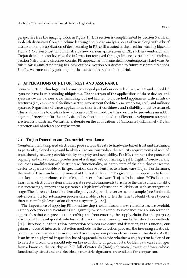
Fig. 6. The sequence of the layers in an IC along with their cross-sectional view [1, 151]
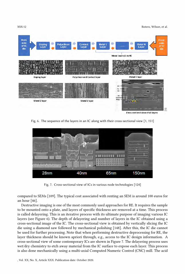
Fig. 7. Cross-sectional view of ICs in various node technologies [124]
compared to SEMs [109]. The typical cost associated with renting an SEM is around 100 euros foran hour [46].
Destructive imaging is one of the most commonly used approaches for RE. It requires the sampleto be mounted onto a plate, and layers of specific thickness are removed at a time. This processis called delayering. This is an iterative process with its ultimate purpose of imaging various IClayers (see Figure 6). The depth of delayering and number of layers in the IC obtained using across-sectional image of the IC. The cross-sectional view is obtained by vertically slicing the ICdie using a diamond saw followed by mechanical polishing [148]. After this, the IC die cannotbe used for further processing. Note that when performing destructive deprocessing for RE, thelayer thickness should be known apriori through, e.g., access to the IC design information. Across-sectional view of some contemporary ICs are shown in Figure 7. The delayering process useswet/dry chemistry to etch away material from the IC surface to expose each layer. This processis also done mechanically using a multi-axial Computed Numeric Control (CNC) mill. The acid
, Vol. XX, No. X, Article XXX. Publication date: October 2020.
Hardware Trust and Assurance through Reverse Engineering:XXX:13
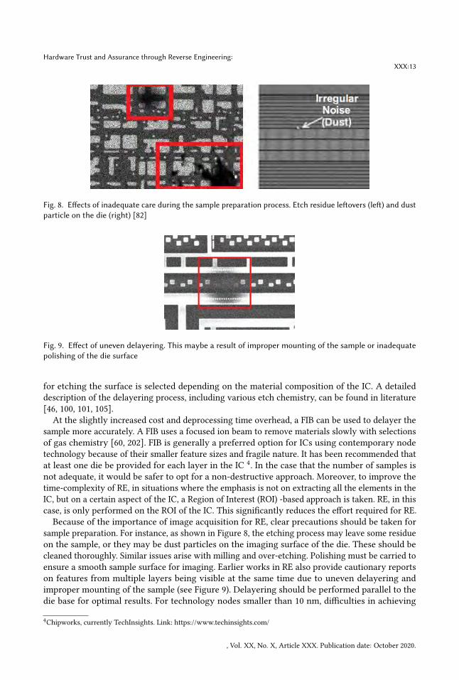
Fig. 8. Effects of inadequate care during the sample preparation process. Etch residue leftovers (left) and dustparticle on the die (right) [82]
Fig. 9. Effect of uneven delayering. This maybe a result of improper mounting of the sample or inadequatepolishing of the die surface
for etching the surface is selected depending on the material composition of the IC. A detaileddescription of the delayering process, including various etch chemistry, can be found in literature[46, 100, 101, 105].
At the slightly increased cost and deprocessing time overhead, a FIB can be used to delayer thesample more accurately. A FIB uses a focused ion beam to remove materials slowly with selectionsof gas chemistry [60, 202]. FIB is generally a preferred option for ICs using contemporary nodetechnology because of their smaller feature sizes and fragile nature. It has been recommended thatat least one die be provided for each layer in the IC 4. In the case that the number of samples isnot adequate, it would be safer to opt for a non-destructive approach. Moreover, to improve thetime-complexity of RE, in situations where the emphasis is not on extracting all the elements in theIC, but on a certain aspect of the IC, a Region of Interest (ROI) -based approach is taken. RE, in thiscase, is only performed on the ROI of the IC. This significantly reduces the effort required for RE.Because of the importance of image acquisition for RE, clear precautions should be taken for
sample preparation. For instance, as shown in Figure 8, the etching process may leave some residueon the sample, or they may be dust particles on the imaging surface of the die. These should becleaned thoroughly. Similar issues arise with milling and over-etching. Polishing must be carried toensure a smooth sample surface for imaging. Earlier works in RE also provide cautionary reportson features from multiple layers being visible at the same time due to uneven delayering andimproper mounting of the sample (see Figure 9). Delayering should be performed parallel to thedie base for optimal results. For technology nodes smaller than 10 nm, difficulties in achieving
4Chipworks, currently TechInsights. Link: https://www.techinsights.com/
, Vol. XX, No. X, Article XXX. Publication date: October 2020.

XXX:14 Botero, Wilson, et al.
Fig. 10. Front-side vs. Back-side deprocessing workflow [149]
proper mechanical polishing and the tendency for surface damage have been reported in a casestudy [174].In a typical RE process, the delayering operation is performed from the frontside of the IC.
The frontside of the IC begins with the lowest metal layer in the structure. Being a well knownapproach, there are counter RE measures installed on ICs to prevent frontside RE [27]. Althoughthis countermeasure can be bypassed by a skilled operator using existing delayering methods,critical damages to the IC under deprocessing could be caused [174]. An alternative to frontside REis the backside RE. At present, there are no known countermeasures to backside RE [101]. Initiallydeveloped as an approach for live-probing an IC under test for fault analysis, backside deprocessinghas also been utilized for IC RE. A complete workflow for both approaches is shown in Figure 10.Apart from the obvious advantage of safer sample deprocessing, the backside approach can alsobe fully automated [149]. A major drawback of backside deprocessing is the die warpage. Withmost of the bulk silicon substrate at the backside of the IC, deprocessing results in an increasedmechanical stress on the die, causing it to warp. This phenomenon is shown in Figure 11. Thesample preparation and delayering process typically take half a day to complete [47]. A detailedbreakdown of the sample preparation time frame from a case study is shown in Table 1. The FIB wasintroduced earlier for safer deprocessing. Although it can be used for both frontside and backsidedeprocessing, it is predominantly used for backside deprocessing. As shown in Figure 7, in typicalICs, the frontside is packed with thick metal layers. Being a process designed for precise removal ofmaterials, FIB editing takes a considerable amount of time to get through the thick metal layers. Forbackside deprocessing, the bulk of the silicon substrate can be removed using simple mechanicalpolishing after the thickness of the silicon substrate is identified using a cross-sectional view. Thelast few nanometers of the silicon substrate can be handled using FIB for precise and time-efficientdeprocessing.
4.1.2 Imaging. Destructive RE is the most common approach in the RE community. Being aniterative procedure, as illustrated in Figure 4, delayering and imaging are done in an alternatingfashion to acquire images of all layers in the IC. As mentioned earlier, SEM is the most commonimaging modality used in RE, owing to its simplicity and ease of access. Consequently, we will
, Vol. XX, No. X, Article XXX. Publication date: October 2020.
Hardware Trust and Assurance through Reverse Engineering:XXX:15
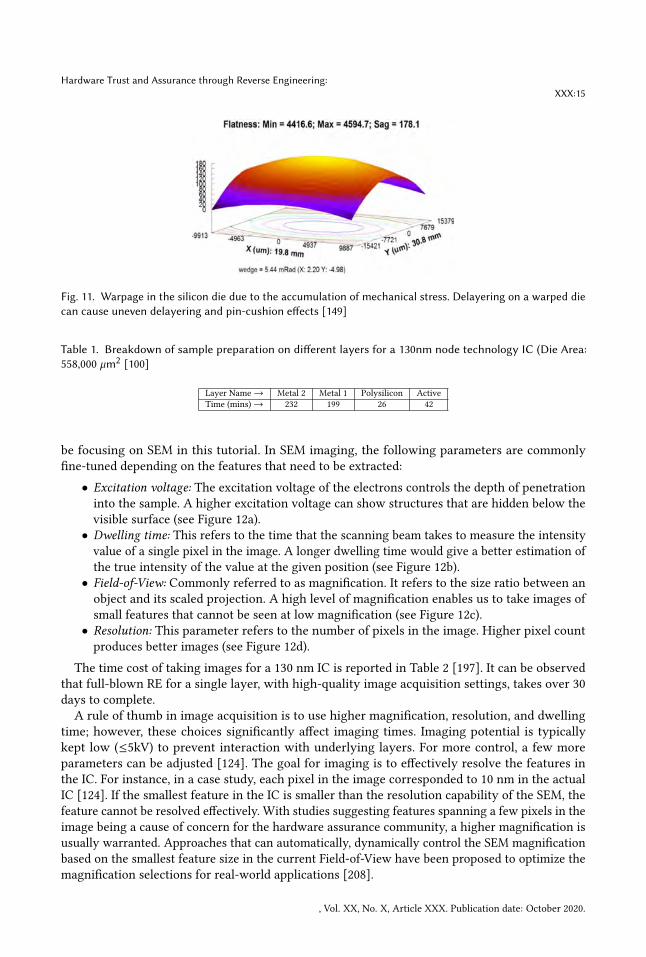
Fig. 11. Warpage in the silicon die due to the accumulation of mechanical stress. Delayering on a warped diecan cause uneven delayering and pin-cushion effects [149]
Table 1. Breakdown of sample preparation on different layers for a 130nm node technology IC (Die Area:558,000 µm2 [100]
Layer Name→ Metal 2 Metal 1 Polysilicon ActiveTime (mins)→ 232 199 26 42
be focusing on SEM in this tutorial. In SEM imaging, the following parameters are commonlyfine-tuned depending on the features that need to be extracted:
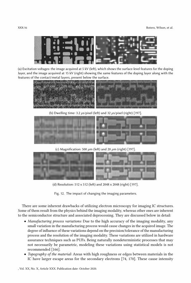
• Excitation voltage: The excitation voltage of the electrons controls the depth of penetrationinto the sample. A higher excitation voltage can show structures that are hidden below thevisible surface (see Figure 12a).
• Dwelling time: This refers to the time that the scanning beam takes to measure the intensityvalue of a single pixel in the image. A longer dwelling time would give a better estimation ofthe true intensity of the value at the given position (see Figure 12b).
• Field-of-View: Commonly referred to as magnification. It refers to the size ratio between anobject and its scaled projection. A high level of magnification enables us to take images ofsmall features that cannot be seen at low magnification (see Figure 12c).
• Resolution: This parameter refers to the number of pixels in the image. Higher pixel countproduces better images (see Figure 12d).
The time cost of taking images for a 130 nm IC is reported in Table 2 [197]. It can be observedthat full-blown RE for a single layer, with high-quality image acquisition settings, takes over 30days to complete.A rule of thumb in image acquisition is to use higher magnification, resolution, and dwelling
time; however, these choices significantly affect imaging times. Imaging potential is typicallykept low (≤5kV) to prevent interaction with underlying layers. For more control, a few moreparameters can be adjusted [124]. The goal for imaging is to effectively resolve the features inthe IC. For instance, in a case study, each pixel in the image corresponded to 10 nm in the actualIC [124]. If the smallest feature in the IC is smaller than the resolution capability of the SEM, thefeature cannot be resolved effectively. With studies suggesting features spanning a few pixels in theimage being a cause of concern for the hardware assurance community, a higher magnification isusually warranted. Approaches that can automatically, dynamically control the SEM magnificationbased on the smallest feature size in the current Field-of-View have been proposed to optimize themagnification selections for real-world applications [208].
, Vol. XX, No. X, Article XXX. Publication date: October 2020.
XXX:16 Botero, Wilson, et al.
(a) Excitation voltages: the image acquired at 5 kV (left), which shows the surface-level features for the dopinglayer, and the image acquired at 15 kV (right) showing the same features of the doping layer along with thefeatures of the contact/metal layers, present below the surface.
(b) Dwelling time: 3.2 µs/pixel (left) and 32 µs/pixel (right) [197].
(c) Magnification: 500 µm (left) and 20 µm (right) [197].
(d) Resolution: 512 x 512 (left) and 2048 x 2048 (right) [197].
Fig. 12. The impact of changing the imaging parameters.
There are some inherent drawbacks of utilizing electron microscopy for imaging IC structures.Some of them result from the physics behind the imaging modality, whereas other ones are inherentto the semiconductor structure and associated deprocessing. They are discussed below in detail:
• Manufacturing process variations: Due to the high accuracy of the imaging modality, anysmall variation in the manufacturing process would cause changes in the acquired image. Thedegree of influence of these variations depend on the precision/tolerance of the manufacturingprocess and the resolution of the imaging modality. These variations are utilized in hardwareassurance techniques such as PUFs. Being naturally nondeterministic processes that maynot necessarily be parametric, modeling these variations using statistical models is notrecommended [166].
• Topography of the material: Areas with high roughness or edges between materials in theIC have larger escape areas for the secondary electrons [74, 170]. These cause intensity
, Vol. XX, No. X, Article XXX. Publication date: October 2020.

Hardware Trust and Assurance through Reverse Engineering:XXX:17
Table 2. Time table of SEM imaging for an IC with the following characteristics: technology node: 130nm,and size: 1.5 mm x 1.5 mm [197]
Scanning Speed Field of ViewResolution 500um x 500um 20um x 20um
1 usec/pixel 512x512 9 sec 1 hr 33 min1 usec/pixel 1024x1024 18 sec 3 hr 7 min1 usec/pixel 2048x2048 54 sec 9 hr 22 min10 usec/pixel 512x512 45 sec 7 hr 48 min10 usec/pixel 1024x1024 3 min 18 sec 1 d 10 hr10 usec/pixel 2048x2048 6 min 25 sec 5 d 12 hr32 usec/pixel 512x512 1 min 30 sec 15 hr 0 sec32 usec/pixel 1024x1024 6 min 30 sec 1 d 21 hr32 usec/pixel 2048x2048 24 min 0 sec 11 d 1 hr100 usec/pixel 512x512 4 min 48 sec 2 d 2 hr100 usec/pixel 1024x1024 18 min 54 sec 8 d 4 hr100 usec/pixel 2048x2048 1 hr 11 min 30 d 20 hr
Fig. 13. Electron migration (left) due to accelerated life cycle conditions causing variations in intensitiesmeasured for the same material [57]. Charging effects (right) exhibited in insulating materials under SEMobservation [82]
variations of the same material measured in different locations on the same IC die. Thisfurther emphasizes the need for polishing and planar surface on the deprocessed IC die.
• Oxidation: Delayering exposes the metallic structures in the IC to the atmosphere [174].Oxidation of metallic surfaces causes fluctuations in the responses obtained for the samematerial at various points in the IC.
• Electron-migration: If the IC has been under use, there are chances of having electronmigrationand changes in the physical structure of the material [57]. This type of defect is usually foundin metal interconnects, through which high-density currents flow (see Figure 13). This issueis predominantly studied in device failure analysis in estimating the lifetime of an IC [129].
• Conductivity: Insulating materials may charge positively and suppress the secondary electrons[74]. This leads to localized pockets of bright and dark regions in the image (see Figure 13).This issue can be offset by depositing thin layers of conductive materials such as carbon orplatinum on the IC die surface [105, 152]. Moreover, if the material is considerably thin, theelectrons can pass through so that the sensors cannot detect them [165]. It should also benoted that when using an active mode of imaging, radiation exposure over a long duration at aspecific location causes a contamination layer to build up over the exposed region, preventingfurther emission of electrons for effective imaging [170].
Several other issues that are predominantly associated with electron microscopy are illustratedin Figure 14 as an exemplary case.
, Vol. XX, No. X, Article XXX. Publication date: October 2020.

XXX:18 Botero, Wilson, et al.
Fig. 14. Practical limitations of electron microscopy techniques. The raw image is shown on left and themiddle one is corrupted with drift and vibration. Rightmost image is corrupted with all three noise sources(drift, vibration, and radiation dose). Context: Gold particles on carbon surface [39].
Fig. 15. Stitching error in the active layer due to improper image registration
• Drift: It is present in every EM modality and cannot be fully accounted for in every case. Itoccurs mainly due to random fluctuations in the scanning beam andmechanical creep inducedby the staging platform of the SEM. Drift is more pronounced at a lower magnification thatcovers a larger Field-of-View [39].
• External Environment: Vibrations, even those that are barely perceptible, along with thermalexpansions in the sample caused by slight temperature fluctuations in the environment, cansignificantly affect image quality [39].
• Radiation dose: This specific aspect of imaging is controlled by the dwelling time of thebeam over a given pixel. In simple terms, longer dwelling times result in better images. Withsignificant development in SEM imaging, especially in scan generators, it is possible to acquiresignificantly better images at lower dwelling times. However, there is a persisting interest inthe community for low-dose imaging to reduce sample damage [64]. There have been severalattempts to model the noise introduced by lower dose imaging in the microscopy community,but the influence of noise in recovering feature in semiconductor RE has not been studied indetail. Currently, there is a consensus agrees on modeling the noise as a Poisson-Gaussianprocess [55, 104, 145, 162, 177].
With regard to the last point, the noise from the electronic components of the SEM (e.g., amplifiersand scan generators) has been modeled as Additive White Gaussian Noise (AWGN), but its influencewas found to be negligible as compared to that of emission noise [14, 192]. It has been suggested thatthe noise introduced by the imaging modalities can be used to hide hardware Trojans [166]. Thisis the motivation behind studying noise in SEM and acquiring good quality images for hardwareassurance applications. The RE workflow has not been optimized for repeatability. Hence, there willalways be unforeseen circumstances during the RE process that would require human interactionto resolve.
, Vol. XX, No. X, Article XXX. Publication date: October 2020.

Hardware Trust and Assurance through Reverse Engineering:XXX:19
Fig. 16. SEM images acquired from a FinFET IC utilizing 14nm node technology. Field-of-View has beenvaried in both images to display contrast in feature sizes. Left: 5µm, Right: 15µm.
In addition to the above issue, when employing SEM, caution regarding the following problemsshould be used.Stitching process: In most cases, the Field-of-View provided by SEM does not cover the entire ROI.This typically results in multiple images to be collected and stitched together to form a completeimage. In typical applications, the stitching process involves taking two images with a certainoverlap. The degree of overlap is decided by the operator and remains fixed for the entire imageacquisition phase. Similarity measures like normalized cross-correlation [124] or features like ScaleInvariant Feature Transforms (SIFT) [153] are used to find the position with the highest correlation.Then the two images are merged by blending the overlapping region or by just using one of theoverlapping regions and discarding the other. Stitching is usually an error-prone process, wherethe error can usually be resolved by a subject-matter expert. There have been attempts at usingmore advanced approaches for improving stitching accuracy.
Nevertheless, stitching for contemporary nanoscale node technologies is even more challenging.Specifically, in such modern ICs, especially in metal layers, the features are very much similar andrepetitive, causing significant corruption in the stitching process. Correlation analysis and Fourierdomain analysis have been conducted in some studies to demonstrate this issue [207, 217]. Aningenious approach has been suggested utilizing leftover imperfections from the delayering processto stitch images with similar features [217]. These imperfections in deprocessing are usually veryunique and unlike inherent features in the IC under study. This work also discusses the issueswith stitching images in all directions on the same plane and the importance of optimizations forensuring the best fit among neighboring images in the plane. An example of a stitching error isshown in Figure 15.Alignment process: The images taken from layers are stacked on top of each other. The alignmentis done using correlation matching, typically involving vertical interconnects (VIA). Design rulechecks and manual operator intervention validate the vertical alignment of the image stack. Thereare several software suites that are available to ensure seamless alignment and viewing of imagessuch as Chipwork’s IC Browser [193], AIRE [23], Olyvia [105] and Hugin [46].Emerging technologies: Although there is no exemplary work done for RE on contemporarytechnologies such as FinFET, some key insight can be obtained from challenges faced by the FaultAnalysis community [143]. Some dielectric materials have low contrast with the silicon substratemaking them harder to identify. A similar situation is shown in Figure 16 with the contrast betweenthe contacts and the metal layers significantly reduced as compared to previous node technologies.This makes it considerably harder to visually analyze the image and hinders contrast-based imageanalysis techniques. It has also been suggested that samples sustain more damage under typical
, Vol. XX, No. X, Article XXX. Publication date: October 2020.
XXX:20 Botero, Wilson, et al.
radiation dose as compared to older node technologies. There are studies that combine simulation-based methods with SEM imaging for higher quality images at lower radiation dose. These hybridmethods are shown to be effective for recent node technologies. This further emphasizes the needfor better noise models for noise-free image acquisition at lower dwelling times. Finally, thereare challenges associated with deprocessing layers with very fine features. With a higher levelof integration in ICs such as 3DVLSI, a full-scale RE workflow would be a daunting task withoutsignificant automation in imaging, deprocessing, and error resolution. The challenges related toperforming RE on post-CMOS technology nodes are yet to be explored.Anote on the positive side of SEM: A limitation of data-driven approaches is the unavailability ofgood quality data, as stated earlier. To address this, the electron microscopy community introducedan SEM image simulator called ARTIMAGEN [39, 40]. However, in recent years, there have beenattempts to generate synthetic data for evaluating data-driven approaches. This simulator cangenerate images with varying influences of drift, vibration, thermal expansion, and noise profiles(Gaussian/Poisson). However, the selection of materials, noise profiles, and shape contours arelimited. The fault analysis community extensively uses simulated images for benchmarking LineEdge/Width Roughness (LER/LWR) algorithms [30]. A deep learning approach has been recentlysuggested to generate synthetic SEM images based on layout data for mask optimization and virtualmeteorology [171]. Although the data used for these approaches are not publicly available, it doesprovide a path towards integrating data-driven approaches for RE in the imaging phase.When it comes to applications of SEM in RE, there are some commercial solutions available.
Notable devices include the Multi-SEM (mSEM) [95] from Zeiss for using multiple scanning beamsfor faster high quality image acquisition and Chipscanner 150 [124] from Raith for use in large-scale image acquisition with higher accuracy requirement on stitching. In contrast to the timingrequirement shown in Table 2, Chipscanner 150 has a reported scan time of 4.9 hours for imagingat 4000x4000 resolution with a 40µm field-of-view on a 1mm2 area [124]. In the same work, thisscan time was brought down to 0.7 hours with a better scan generator. Although convenient, thesesystems are also significantly more expensive than regular SEMs [194]. The computational resourcecomplexity is also an attention-worthy aspect of RE. For instance, the storage complexity associatedwith acquiring images of the entire active layer of a 45nm node technology IC has been estimated tobe over 22 gigabytes on regular SEMs [44]. For high-performance imaging systems like the mSEM,this requirement is much higher [217].
4.2 Problems Associated with Handling PCB ImagesAs opposed to what has been explained for ICs in Section 4.1, the imaging process performedon PCBs does not require decapsulation. However, components mounted on the PCB can beremoved for easier access to the PCB markings and easier imaging for multi-layered PCBs. The PCBequivalent of decapsulation in ICs is referred to as de-soldering, or the removal of componenteson the PCB. The byproduct of this de-soldering is varying levels of collateral damage to the PCB,depending on the efficacy of the decapsulation process. This will have different impacts on laterstages of RE, such as image acquisition, where the damages are reflected in the form of debris,physical distortion, or noise artifacts present in the digital image. Therefore, it is recommended toavoid de-soldering when possible, but if necessary, it should be done with the utmost care as tolimit the damage to other key features (trace tracks, via conductive rings, text markings on PCBsurface, etc.).
The challenges and limitations associated with PCB RE overlap significantly with those presentedearlier in IC RE scenarios. The main difference is that PCB RE has two focused aspects: external andinternal RE. External PCB RE deals with the information that one can observe at both surfaces, the
, Vol. XX, No. X, Article XXX. Publication date: October 2020.

Hardware Trust and Assurance through Reverse Engineering:XXX:21
top and bottom layers of a PCB. This information typically consists of the components of a design(passive elements, active elements, ICs, processors, etc.), their connections, silkscreen markings, anda variety of ports [151]. External RE would usually suffice if the PCB has only two layers, but thisis often not the case. More common, however, are PCBs manufactured with multiple layers, wherethe majority of them are internal to the board and have structural and connectivity informationnot visible externally. In these cases, internal RE is necessary [151].
Traditionally, internal RE has been a destructive process [69] similar to that of IC RE. The processinvolves delayering and imaging of a PCB layer-by-layer until a working functional physical sampleno longer exists. The imaging component of this process is typically done optically by using adigital camera or a high-quality optical microscope, but the destructive nature of the delayeringprocess introduces multiple potential sources of the noise that could impact the quality of the image.Some examples include broken traces, disconnected vias, or poor quality images, making featureextraction much more difficult for analysis. These features need to be imaged to the highest degreeof detail possible to facilitate optimal performance in the RE process, which is usually bound bythe quality of the image under analysis. Fortunately, recent progress toward non-destructive REvia X-Ray CT has pushed the current state-of-the-art RE methods [6].
4.2.1 Imaging. The main challenges for each PCB RE modality can be broadly categorized intohow to handle the noise associated with the imaging modality used for data acquisition.We expandon these issues for both the external and internal RE, as defined above.External RE: The imaging modality used for data acquisition in external PCB RE is typically anoptical microscope or a digital camera. Both are used to take images of a PCB at varying resolutionsto enable the detection, classification, and analysis of the design information. Specifically, externalRE uses these images to identify the components, connections, silkscreen markings, and differenttypes of ports (high-speed serial/parallel, program/debug, display) present on the topside as wellas bottomside of a PCB [69, 193]. Among all imaging modalities, the illumination variance is themost prominent noise source. In some cases, imaging an entire PCB board requires stitching,which results in multiple regions of the entire board with varying illuminance. This variationmay cause differences in the appearance of even the same sample; therefore, drastically impactingthe effectiveness of image analysis algorithms and the inspection results. Hence, a dedicatedoptical imaging station that provides consistent illumination across the entire imaged board isrecommended. The dedicated imaging station should consist of a constant light source that is welldistributed across an area. For example, a hanging lamp in combination with a high-resolutionDSLR camera can be used to equip a larger station and an optical microscope station used for smallto medium samples.Depending on the magnification of the microscope or camera used for data acquisition, the
image patches obtained vary in size and the amount of information included in them. While anincrease in the magnification obtains more detailed features for extraction, the illumination noiseis also amplified (see Figure 17), causing an information loss. For instance, using low magnificationresults in a larger image view, but we may lose small features (e.g., characters on resistor) dueto the reflection. This could make the detection of Trojans, i.e., maliciously inserted/replacedcomponents, more challenging. Although more features per image lead to more details, more imagepatches should be stitched together to complete the whole image, and thus, regions with the variousilluminance are involved in the fully stitched sample.On the contrary, when the image magnification increases to obtain more details, some large
components on a PCB are separated into different patches. Moreover, since many of the existing
, Vol. XX, No. X, Article XXX. Publication date: October 2020.

XXX:22 Botero, Wilson, et al.
Fig. 17. Optically imaged PCB section highlighting illuminance non-uniformity
Fig. 18. Noise in X-Ray CT PCB:(red square on the right side) Neighboring Layers Aliasing (green square onthe bottom left side) Blur Artifacts (yellow square on the top left side) High Impedance Material Artifacts
image analysis algorithms for segmentation, detection, and classification are heavily parameter-dependent or pixel intensity sensitive [2, 48, 91, 93, 128, 169], a holistic solution for PCB RE that ismore generalizable by minimizing parameter tuning is needed.Internal RE: If the PCB under RE has only one to two layers, the challenges encountered by theexpert would be solely limited to those discussed above. However, it is more likely that modernPCBs are multilayered, where chips are connected to each other on the top, bottom, and throughinternal layers. Therefore, for multilayered PCBs, internal RE is required to complete the RE process.When discussing internal RE, there are two predominant methods: destructive and non-destructiveRE. As explained earlier, the destructive approach is obsolete by contemporary standards and willnot be considered further.While non-destructive RE via X-Ray CT does reduce the amount of physical damage to a PCB
caused by the delayering process, there are other challenges still to be faced, which impact thequality of the RE. These noise sources generated by the X-Ray process are outlined below.
, Vol. XX, No. X, Article XXX. Publication date: October 2020.
Hardware Trust and Assurance through Reverse Engineering:XXX:23
• Blur artifacts: During the X-Ray CT process, the sample is rotated inside the X-Ray chamberby 360°at a slight tilt in the Cartesian plane to maximize the amount of information receivedfrom the X-Ray particles passing through the sample to the receiver in the chamber. Thistilt, along with the rotation during the acquisition process, results in noise artifacts in thereconstructed 3D stack in the form of blurred image regions.
• High impedance materials: Typically, PCBs are manufactured with the majority of theirparts made of silicone-based materials. However, if the PCB is populated with components,soldering is used to ensure the connectivity of the components throughout the entire board.This solder acts as a high impedance material in the presence of X-Ray particles, reducingthe effectiveness of their passing-through property. Therefore, it creates noise artifacts in apopulated sample or a sample with components being removed, but with remaining solderresidue.
• Aliasing between neighboring layers: An X-Ray CT-based PCB model is a 3D stack consistingof 2D image slices. Each layer of a multi-layer PCB consists of the trace and via informationthat may differ from those being close to that layer. Depending on the alignment of the boardin the X-ray chamber, the resolution, and the X-Ray parameters chosen, there may be slicesat the fringes of neighboring layers, where the information of the layers overlaps, similar toaliasing in signal processing.
• Beam hardening: While an X-Ray beam passes through an object, the mean energy of thebeam increases as the low energy photons are attenuated [17]. Therefore, the lower energypart of the X-ray beam is removed from its energy spectrum, and the beam is consideredto become “harder". Due to this X-ray beam hardening, streaks or dark bands appear at thecenter of the object, compared to the edge of the object in the X-ray image. For this purpose,pre/post-filtering the X-Ray beam by using metallic materials, e.g., aluminum and copper,is applied to eliminate the low energy photons in the beam and maintain uniform averageenergy during the X-ray imaging.
• Ring artifact: In general, miscalibrated or defective detectors and elements create a brightor dark ring close to the isocenter of the scan. This can often be fixed by recalibrating thedetector.
The blur caused by the X-Ray is seen as the streaks in the image (see the green square on thebottom left side of Figure 18). The bright circular regions are where the solder has impacted theX-Ray process, distorting the via features slightly, as illustrated in the yellow part on the top leftside of the figure. The areas, where the trace information is intersecting each other, show aliasingthat occurs between the neighboring layers (see the red square on the right side of Figure 18).While these are the main sources of the noise seen during the X-Ray process conducted on a PCB,their effects are compounded when taking the reconstruction process for X-Ray CT into account.In particular, at each slice of the reconstructed PCB, crafted by using X-Ray CT, the noise sourceshave a varying degree of impact since they represent the varying depths of the board and thedepth of the X-Ray particles passing through the samples. Therefore, it is necessary for imageanalysis-related solutions to not only account for the variance seen within a single design, butalso across multiple designs. Nonetheless, the impact of the noise could be reduced by adjustingparameters discussed below.
• Tube voltage: This parameter adjusts the peak energy of the X-Ray beam (i.e., raises theaverage energy of the photons). The choice of the tube voltage affects the image contrast inthe scanning process. An increase in this voltage leads to a lower contrast in the images.
, Vol. XX, No. X, Article XXX. Publication date: October 2020.

XXX:24 Botero, Wilson, et al.
Table 3. Resolution limits of imaging modalities and associated processes discussed in this tutorial
Imaging Modality→ SEM FIB X-ray CT Optical (DSLR)Resolution limits→ 2nm 15nm 1-2µm for ICs/ 10-50µm for PCBs/ 50-100nm for wafer-level samples 85µm
• Tube current-exposure time product: This refers to the number of photons produced per unittime. Random, thin, bright and dark streaks are considered as noise that may appear in theimages due to the low photon counts.
• Resolution: The resolution of the image is defined as the pixel size selected during X-Rayimage acquisition, where the pixel size can be identified as the limiting factor for spatialresolution.
• Filtration: Filters are used to reduce the beam hardening effects in the X-Ray beam. As thelow-energy photons do not penetrate through the object, filtration improves the quality ofthe beam.
For the sake of comparison, Table 3 provides the resolution limits of the imaging modalities andassociated processes discussed in this section.
5 ADDRESSING CHALLENGES ASSOCIATEDWITH MACHINE LEARNING ANDIMAGE ANALYSIS FOR RE
In the context of natural scenes, image processing plays the role of enhancing the image to thepoint of being discernible and pleasing to the viewer. The fine-tuning of different image parameters,such as the contrast and intensity, is considered as an art rather than an application of a set ofpredefined algorithms. However, with the advent of machine learning and the higher likelihood ofthe image being delivered to a computer than a human, the adjustment of the imaging parametersmust be performed regarding the application for a particular domain and nature of the problembeing addressed. For instance, a camera placed on an assembly line in a manufacturing facilitymight only require to examine the presence of an object rather than its color or shape. Modifyingthe image to be visually pleasing is neither required nor recommended in this case.
Optimizing images for a certain purpose requires in-depth knowledge of the domain and applica-tion, posing a significant challenge to the application of image processing in electronics, e.g., imagestaken from ICs or PCBs. It is reasonable to say that almost any data-driven approach, especiallymachine learning and image analysis, has its performance limited to the quality of the data providedto it. For instance, in the case of IC RE, the importance should be placed on electrical connectivityrather than visual quality. Assessing data quality using existing measures such as Signal-to-Noise(SNR) ratio does not provide insight into the true quality of the sample. Hence, invalidating theinsight obtained using such samples.
Along with the extensive application of image processing in natural scene-related scenarios, thefactors affecting the quality of images, such as motion blur, sensor noise, and uneven lighting, arewell known and studied. This in-depth understanding enables the development of image processingalgorithms that can suppress the effect of noise sources, as mentioned above, and produce high-quality images. However, this does not hold true for imaging modalities used for acquiring imagesof ICs and/or PCBs. Hence, the wealth of knowledge compiled over time in the field of imageprocessing cannot be effectively utilized for RE and hardware assurance.
Moreover, in typical natural scene images, the amount of information extracted is rarely depen-dent on the value of a few pixels, but on the entire image or a large section of the image. On theother hand, by increasing the level of integration that puts together a higher number of transistorsinto a limited space, the size of the features in an IC image usually expands to only a few pixels (seeFigure 19 (a, b)). An analogous task for PCB RE is detecting vias and traces in a densely populated
, Vol. XX, No. X, Article XXX. Publication date: October 2020.

Hardware Trust and Assurance through Reverse Engineering:XXX:25
Fig. 19. Difficulties with the handling of IC images: (a) an SEM image of a logic cell showing the size offeatures in pixels, (b) the software-based structure of the cell shown in (a), and (c) an example illustrating theambiguity in the feature resolution in the presence of the noise.
image where these features and structures can be only a few pixels long or wide. Hence, dependingon the intensity of noise affecting such features, there are situations, where a structure containinga few pixels cannot be categorized into a feature or a noise artifact (see Figure 19 (c)). In the contextof hardware assurance, this ambiguity may result in miss classification of a Trojan. Similarly, PCBimages used for RE are subject to this challenge, albeit in a different way, due to the differentmodalities the images are taken from. For instance, optical imaging can easily fail to detect an extracomponent acting as a Trojan, when the color of the motherboard and the components on it areboth black. Furthermore, via detection through X-Ray CT imaging may not be helpful when viasare blurred by the presence of high impedance materials that attenuate X-rays.Challenges that can be resolved through machine learning have three factors in common: a
coarse understanding of the problem, the availability of high quality labeled/unlabeled data, andunderstanding of the statistical features that can assist in quantifying/representing the problem.With hardware designers and manufacturers having design experiences that are specific to them, itcould be hard to find features that can be generalized to all cases. Even in approaches that supportautomated feature discovery, such as artificial neural networks, a significant amount of labeled datais required. In many instances, obtaining such ground truth is either not possible (obsolescence) orimpractical (pixel-level labeling for semantic segmentation) due to the time and resources required.With issues compounding on every basic step of the machine learning paradigm, a holistic approachthat can effectively cover all RE workflow stages is extremely challenging.The inherent complexity of using ML for RE can be demonstrated with a simple example. The
steps involved in designing an IC usually start with a high-level description of all the modules. Thesemodules are synthesized with standard cell libraries from IC manufacturers. The design is thenplaced, routed, and etched onto a silicon wafer die [59]. In machine learning terminology, this wholeprocess is akin to performing a dimensionality reduction technique, such as Principal ComponentAnalysis (PCA), on the raw data. More specifically, although the processed low dimensional databehaves in the same fashion as the raw data and can be considered equivalent, recovery of theoriginal data from a low dimensional projected version is hard.The goal of most RE applications is broadly classified into three types: recovery of schematics,
obtain insights into the design, and to detect anomalies in the design for hardware assurancepurposes. In order to satisfy these goals, the constraints on applying data-driven methods will have
, Vol. XX, No. X, Article XXX. Publication date: October 2020.

XXX:26 Botero, Wilson, et al.
Fig. 20. Expanded workflow for the Annotation block
to be relaxed and explored within individual modules in the RE workflow, where the strengthsof image processing and machine learning can be effectively utilized. In the following sections,we will explore various approaches that can get the reader as close to the original design data aspossible.
5.1 Problems Associated with Applying ML for IC REThe applications of ML algorithms in IC RE mainly include two types of methods employed toperform annotation and extract the netlist5, described in this section.
5.1.1 Annotation. The annotation module expects image data from the previous step to be noise-free, free of deprocessing errors, well stitched, and aligned in all layers. However, in most cases, theseare not fully satisfied. The annotation module can be divided into three sub-modules: denoising,segmentation, and vectorization. An overview of the annotation block can be seen in Figure 20.
Prior to denoising the image, it is necessary to ensure that the image contents are not corruptedfrom deprocessing and stitching errors. Currently, there are no approaches to detect corruptedimages. However, some insights can be obtained by looking into the forward manufacturingworkflow. For instance, stitching errors may be corrected using design rule checks. Deprocessingerrors are similar to faults in the IC die. There are quality control and design validation approachesthat utilize image processing and pattern recognition to detect such faults. These approaches canbe re-purposed for detecting deprocessing errors in the RE workflow [137, 203].Denoising: The denoising sub-module is responsible for ensuring that the noise component in theimage is suppressed. There are several approaches currently employed in literature for processingnoisy SEM images. They include spatial filtering approaches, including Gaussian, median, curvature,anisotropic diffusion, wavelet, adaptive wiener filter, and hysteresis smoothing [5, 130, 132, 195].Simple high-frequency filtering and deep learning-based denoising approaches have also beenused on SEM images [64]. These techniques are mostly naive image processing techniques and donot take the semantics of structures in the image into account. Machine learning-based denoising5A netlist is a graph that shows relationships between various components.
, Vol. XX, No. X, Article XXX. Publication date: October 2020.
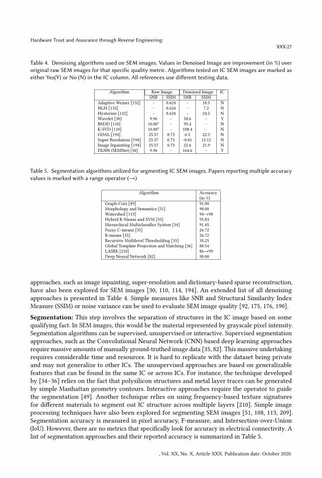
Hardware Trust and Assurance through Reverse Engineering:XXX:27
Table 4. Denoising algorithms used on SEM images. Values in Denoised Image are improvement (in %) overoriginal raw SEM images for that specific quality metric. Algorithms tested on IC SEM images are marked aseither Yes(Y) or No (N) in the IC column. All references use different testing data.
Algorithm Raw Image Denoised Image ICSNR SSIM SNR SSIM
Adaptive Weiner [132] - 0.624 - 18.5 NNLM [132] - 0.624 - 7.2 NHysterisis [132] - 0.624 - 24.2 NWavelet [30] 9.96 - 58.6 - YBM3D [110] 10.00* - 95.4 - NK-SVD [110] 10.00* - 108.4 - NGOAL [194] 25.57 0.73 6.5 22.3 NSuper Resolution [194] 25.57 0.73 -0.01 12.12 NImage Inpainting [194] 25.57 0.73 22.6 21.9 NDLNN (SEMNet) [30] 9.96 - 164.6 - Y
Table 5. Segmentation algorithms utilized for segmenting IC SEM images. Papers reporting multiple accuracyvalues is marked with a range operator (→)
Algorithm Accuracy(in %)
Graph-Cuts [49] 91.00Morphology and Semantics [51] 90.00Watershed [113] 94→98Hybrid K-Means and SVM [35] 95.83Hierarchical Multiclassifier System [34] 91.45Fuzzy C-means [35] 26.72K-means [35] 26.72Recursive Multilevel Thresholding [35] 35.25Global Template Projection and Matching [36] 88.54LASRE [210] 86→99Deep Neural Network [82] 98.00
approaches, such as image inpainting, super-resolution and dictionary-based sparse reconstruction,have also been explored for SEM images [30, 110, 114, 194]. An extended list of all denoisingapproaches is presented in Table 4. Simple measures like SNR and Structural Similarity IndexMeasure (SSIM) or noise variance can be used to evaluate SEM image quality [92, 175, 176, 190].Segmentation: This step involves the separation of structures in the IC image based on somequalifying fact. In SEM images, this would be the material represented by grayscale pixel intensity.Segmentation algorithms can be supervised, unsupervised or interactive. Supervised segmentationapproaches, such as the Convolutional Neural Network (CNN) based deep learning approachesrequire massive amounts of manually ground-truthed image data [35, 82]. This massive undertakingrequires considerable time and resources. It is hard to replicate with the dataset being privateand may not generalize to other ICs. The unsupervised approaches are based on generalizablefeatures that can be found in the same IC or across ICs. For instance, the technique developedby [34–36] relies on the fact that polysilicon structures and metal layer traces can be generatedby simple Manhattan geometry contours. Interactive approaches require the operator to guidethe segmentation [49]. Another technique relies on using frequency-based texture signaturesfor different materials to segment out IC structure across multiple layers [210]. Simple imageprocessing techniques have also been explored for segmenting SEM images [51, 108, 113, 209].Segmentation accuracy is measured in pixel accuracy, F-measure, and Intersection-over-Union(IoU). However, there are no metrics that specifically look for accuracy in electrical connectivity. Alist of segmentation approaches and their reported accuracy is summarized in Table 5.
, Vol. XX, No. X, Article XXX. Publication date: October 2020.

XXX:28 Botero, Wilson, et al.
Fig. 21. Edge distortion caused by limitations in the mask generation process in transition from the GDSIIlayout (left) to the silicon wafer (right) [171]
Vectorization: Finally, the vectorization stage converts the image into a bunch of polygons. Theidea behind this module is to recover design files as close to the original die layout as possible. Thisspecific step enables the use of commercial off-the-shelf tools allowing smoother transition betweenthe annotation and the netlist extraction modules. This step further serves in suppressing edgenoise between materials (discussed in detail with EWR/LWR for FA [43, 134, 146]) and compressingthe amount of data in the image. Vectorization has been achieved through simple edge followingalgorithms, supervised learning via XGBoost, and even deep learning [16, 152]. It should be notedthat edges in the original layout are converted to simple curves in the SEM images (see Figure21). This is due to the mask generation process done for etching the IC onto the wafer duringmanufacturing and not an artifact introduced by the imaging modality or any sample preparationstep [123].
The annotation block is critical to several hardware assurance measures. Being in the middle ofthe RE workflow, the amount of errors accumulated at this stage is far lower than further down theline. Several approaches use segmented images of the IC layers for detecting Trojans. [10, 11] and[139] detect metal layer Trojans using classifiers trained on synthesized images. The former twoworks hand-craft shape features, while the latter one extract histogram of oriented gradients (HOG)features to represent discriminatory characteristics of gates. [196] and [172] apply the Fouriershape descriptor to detect modifications on cells’ appearance from SEM images of the IC’s activelayer. The classifier training in [196] is conducted on a pre-collected IC SEM image dataset, and thetraining in [172] is on SEM images of on-chip electrically authenticated gates.
Other approaches utilize SEM images of the golden IC or layout and simple correlation analysisor template matching to make sure that the sample is Trojan free [45, 197]. Additionally, someapproaches for avoiding Trojan insertion watermark the active layer with highly reflective fillercells. Their combined reflectance signature can be used to make sure that the IC is Trojan-free [221].A similar approach uses thermal maps and deep learning to detect Trojans [206]. Being segmented,hardware assurance measures performed at this stage can also be free of the influence of localizedvariation in pixel intensity and noise, which has been demonstrated in the above works. It shouldalso be noted that variants in Trojans, such as the parametric Trojans, can only be detected at thisstage in RE. The only disadvantage at this stage is the overhead in storing and processing full-scaleimages.
5.1.2 Netlist Extraction. This stage involves the transition from the recovered layout into a netlist.As illustrated in Figure 22, this representation can be obtained at various levels of abstraction:transistor, gate and behavior-levels. This stage has the likelihood of having the most errors inthe entire RE workflow. In contrast to popular belief, netlist extraction and debugging take moretime and manual operator interaction than imaging and annotation modules. With present node
, Vol. XX, No. X, Article XXX. Publication date: October 2020.

Hardware Trust and Assurance through Reverse Engineering:XXX:29
Fig. 22. Expanded workflow for the netlist block. Operator understandability and intrepretability of the REnetlist increases from transistor-level towards behavioural-level netlist
technologies integrating several billion transistors in an IC die, it is reasonable to assume that therea billion opportunities to make mistakes. This is the underlying reason behind the existence ofseveral hardware assurance approaches at the annotation module. However, in order to ensurethat the hardware is completely Trojan free (like small scale Trojans with highly unique activationsequences) and to pave a path towards re-engineering obsolescent ICs, this stage is essential. Inaddition, there are several counter-RE approaches implemented at this stage, making error-free REa daunting task. On a side note, it should be understood that RE is almost always performed ondigital elements in the circuit. Large analog elements are extracted manually by the operator anddecoded by an SME.
Transistor-level netlist can be generated for both digital and analog circuits. But it is predominantlydone in analog circuits. The majority of the exemplary work in digital IC RE skips straight tothe gate-level netlist. The transistor-level netlist is obtained either by simple image processingtechniques like template matching and manual operation interaction. A transistor is detected atthe overlap of diffusion and polysilicon layers in the CMOS technology [22]. The width for then-type CMOS gate is assumed to be smaller than the p-type CMOS gate [123].Gate-level netlists operate by combining several transistors into logic gates. In most cases, the
standard cell library that defines the gates are not available. Hence, with the help of Subject MatterExperts (SME), the operator has to manually identify each cell and use image-based correlation togenerate a standard cell library [100, 141, 153]. Custom feature descriptors are also explored forimproving cell template localization in large scale images [52]. This is a time-consuming process.Recently, an approach has been introduced that uses information from the contact layer to identifythe standard cell library automatically [207]. However, this approach assumes that no obfuscationhas been performed on the cells. The amount of prior information at this stage significantly helpspeed up the RE process. For instance, if the standard cell library is known beforehand, the processof netlist recovery would be easier. For entities that have access to the golden netlist, a simplecomparison can assure that the device under test is Trojan free. The validation of both the extractedtransistor and gate-level netlist is done through simulations and design rules checks. ElectronicDesign Automation (EDA) tool suites, such as those provided by Cadence, are used to performthese checks [152]. A sample time frame for netlist extraction reported in a case study is shown inTable 6.
A behavioral-level netlist is generated to understand the functionality of the circuit itself. Thisfacilitates obtaining insights on the design, especially for competitive intelligence and IP protection.Module functionality and boundaries are recovered at this step. Another one of the core reasons forRE, the recovery of schematics, is performed at this stage. For obsolescent ICs, the RTL descriptioncan be extracted from the gate-level netlist and synthesized into contemporary node technology,which can be manufactured in a fab with or without changes to the existing design. An exemplarywork has been performed for this specific purpose [100]. However, an in-house tool has been used
, Vol. XX, No. X, Article XXX. Publication date: October 2020.
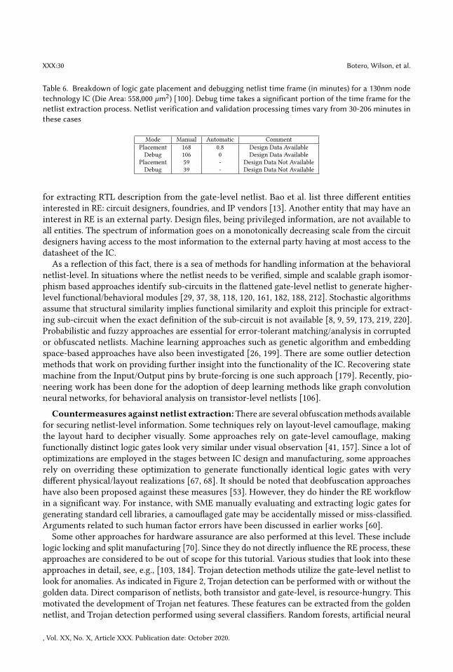
XXX:30 Botero, Wilson, et al.
Table 6. Breakdown of logic gate placement and debugging netlist time frame (in minutes) for a 130nm nodetechnology IC (Die Area: 558,000 µm2) [100]. Debug time takes a significant portion of the time frame for thenetlist extraction process. Netlist verification and validation processing times vary from 30-206 minutes inthese cases
Mode Manual Automatic CommentPlacement 168 0.8 Design Data AvailableDebug 106 0 Design Data Available
Placement 59 - Design Data Not AvailableDebug 39 - Design Data Not Available
for extracting RTL description from the gate-level netlist. Bao et al. list three different entitiesinterested in RE: circuit designers, foundries, and IP vendors [13]. Another entity that may have aninterest in RE is an external party. Design files, being privileged information, are not available toall entities. The spectrum of information goes on a monotonically decreasing scale from the circuitdesigners having access to the most information to the external party having at most access to thedatasheet of the IC.
As a reflection of this fact, there is a sea of methods for handling information at the behavioralnetlist-level. In situations where the netlist needs to be verified, simple and scalable graph isomor-phism based approaches identify sub-circuits in the flattened gate-level netlist to generate higher-level functional/behavioral modules [29, 37, 38, 118, 120, 161, 182, 188, 212]. Stochastic algorithmsassume that structural similarity implies functional similarity and exploit this principle for extract-ing sub-circuit when the exact definition of the sub-circuit is not available [8, 9, 59, 173, 219, 220].Probabilistic and fuzzy approaches are essential for error-tolerant matching/analysis in corruptedor obfuscated netlists. Machine learning approaches such as genetic algorithm and embeddingspace-based approaches have also been investigated [26, 199]. There are some outlier detectionmethods that work on providing further insight into the functionality of the IC. Recovering statemachine from the Input/Output pins by brute-forcing is one such approach [179]. Recently, pio-neering work has been done for the adoption of deep learning methods like graph convolutionneural networks, for behavioral analysis on transistor-level netlists [106].
Countermeasures against netlist extraction:There are several obfuscationmethods availablefor securing netlist-level information. Some techniques rely on layout-level camouflage, makingthe layout hard to decipher visually. Some approaches rely on gate-level camouflage, makingfunctionally distinct logic gates look very similar under visual observation [41, 157]. Since a lot ofoptimizations are employed in the stages between IC design and manufacturing, some approachesrely on overriding these optimization to generate functionally identical logic gates with verydifferent physical/layout realizations [67, 68]. It should be noted that deobfuscation approacheshave also been proposed against these measures [53]. However, they do hinder the RE workflowin a significant way. For instance, with SME manually evaluating and extracting logic gates forgenerating standard cell libraries, a camouflaged gate may be accidentally missed or miss-classified.Arguments related to such human factor errors have been discussed in earlier works [60].
Some other approaches for hardware assurance are also performed at this level. These includelogic locking and split manufacturing [70]. Since they do not directly influence the RE process, theseapproaches are considered to be out of scope for this tutorial. Various studies that look into theseapproaches in detail, see, e.g., [103, 184]. Trojan detection methods utilize the gate-level netlist tolook for anomalies. As indicated in Figure 2, Trojan detection can be performed with or without thegolden data. Direct comparison of netlists, both transistor and gate-level, is resource-hungry. Thismotivated the development of Trojan net features. These features can be extracted from the goldennetlist, and Trojan detection performed using several classifiers. Random forests, artificial neural
, Vol. XX, No. X, Article XXX. Publication date: October 2020.

Hardware Trust and Assurance through Reverse Engineering:XXX:31
Table 7. Performance of Trojan Detection Works
Detection Work Golden data Performance1Accuracy FPR FNR TPR TNR
Image-based
[10, 11] Golden layout 99.9% - - - -[139] Golden layout 89.0% 7.7% - - -[221] Golden layout - 0.5% 1.2% - -[206] Golden layout 98.2% - - - -[172] Golden layout 100% - - - -[196] Golden IC 98.0% 2.0% - - -
[45, 197] Golden IC 100% visually - - - -
Netlist-based
[75] Golden netlist - - - 96.8% 66.3%[76] Golden netlist - - - 85.0% 70.0%[77] Golden netlist - - - 70.3% 99.7%[33] Golden netlist 99.8% - - 89.8% 99.9%[25] Not required 97.5% - 70.3% - -[163] Not required - 0% 0% - -
1 Table presents the averaged reported performance or the best averaged performance if multipleaveraged performance are available. FPR: False Positive Rate, FNR: False Negative Rate, TPR: TruePositive Rate, TNR: True Negative Rate.
Table 8. Commercial and open-source tools available for RE related tasks
Name PurposeARES [189] Segmented image to GDSII layoutPIX2net6 AnnotationDegate [198] Gate recognition and annotationGDS-X [152] Segmentation-to-polygon conversionCircuitFinder [98] AnnotationICWorks [202] Gate netlist extractionHAL [201] Gate netlist manipulation
networks, and SVMs have been explored in this context [33, 75–77]. When direct access to goldennetlists is not available, unsupervised cluster analyses detect Trojan infected circuits as outliers[25, 163]. Another approach using test patterns generated by Automated Test Pattern Generation(ATPG) tools has also been suggested [166]. Since non-invasive Trojan detection methods is outof scope of this tutorial, interested readers are directed to other detailed surveys on the topic[54, 117, 121]. Table 7 lists hardware assurance approaches on both the annotation and netlistextraction modules.Available tools: Unlike the imaging and annotation modules, the netlist extraction module iswell-studied in the literature. There are several benchmark datasets available such as ISCAS [73],TrustHub [164], Synopsis Academic Datasets [65, 66], OpenCores [142], IWLS [4], OSU35 [144] andFreePDK [56] that help generate sample data for hardware assurance applications such as Trojandetection.In recent years, several tools have been introduced that can significantly reduce the workload
associated with RE. A list of these tools can be found in Table 8. One of the three main reasonsfor performing RE is achieved at this level of abstraction: detection of anomalies in the design forhardware assurance purposes. Hardware assurance approaches for post-CMOS technologies areout of scope of this tutorial. Interested readers are directed to recent work by Knechtel for moredetails [102].
5.2 Problems Associated with Applying ML for PCB REHere, similar to our discussion on howML can be useful for IC RE, annotation, and netlist extractiontechniques carried out in the context of PCB RE are explained.
, Vol. XX, No. X, Article XXX. Publication date: October 2020.
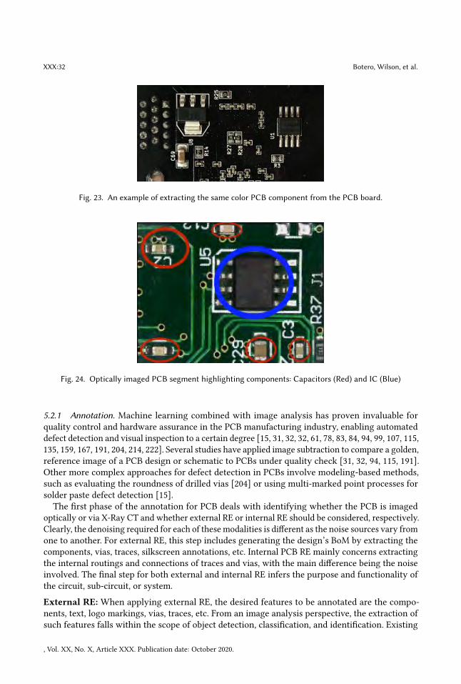
XXX:32 Botero, Wilson, et al.
Fig. 23. An example of extracting the same color PCB component from the PCB board.
Fig. 24. Optically imaged PCB segment highlighting components: Capacitors (Red) and IC (Blue)
5.2.1 Annotation. Machine learning combined with image analysis has proven invaluable forquality control and hardware assurance in the PCB manufacturing industry, enabling automateddefect detection and visual inspection to a certain degree [15, 31, 32, 32, 61, 78, 83, 84, 94, 99, 107, 115,135, 159, 167, 191, 204, 214, 222]. Several studies have applied image subtraction to compare a golden,reference image of a PCB design or schematic to PCBs under quality check [31, 32, 94, 115, 191].Other more complex approaches for defect detection in PCBs involve modeling-based methods,such as evaluating the roundness of drilled vias [204] or using multi-marked point processes forsolder paste defect detection [15].The first phase of the annotation for PCB deals with identifying whether the PCB is imaged
optically or via X-Ray CT and whether external RE or internal RE should be considered, respectively.Clearly, the denoising required for each of these modalities is different as the noise sources vary fromone to another. For external RE, this step includes generating the design’s BoM by extracting thecomponents, vias, traces, silkscreen annotations, etc. Internal PCB RE mainly concerns extractingthe internal routings and connections of traces and vias, with the main difference being the noiseinvolved. The final step for both external and internal RE infers the purpose and functionality ofthe circuit, sub-circuit, or system.External RE: When applying external RE, the desired features to be annotated are the compo-nents, text, logo markings, vias, traces, etc. From an image analysis perspective, the extraction ofsuch features falls within the scope of object detection, classification, and identification. Existing
, Vol. XX, No. X, Article XXX. Publication date: October 2020.

Hardware Trust and Assurance through Reverse Engineering:XXX:33
algorithms for achieving these goals are well-developed for natural scene images [158, 200]. Never-theless, adapting these algorithms for external PCB RE-related applications remains challenging.The components on the surface of a PCB vary in size and color depending on their functionalityand packaging. This could challenge the annotation process. First, the lighting conditions andcolor of PCB surfaces may impact the extraction performance. Traditional image analysis methodsconvert an RGB image to another color map to address the lighting variance [112, 183]; however,this cannot prevent shadowing on PCB surface due to the existence of tall components, which mayresult in an error of using color-based segmentation methods. Moreover, the complications whenthe color of a PCB’s surface is similar to the color of components has not been addressed completely(see Figure 23 where the colors of the surface of the PCB and components are all black). Besides,in an optically imaged PCB, text markings, traces, and vias are packed tightly compared to theobjects in a natural scene image. This increased image complexity challenges feature localization,especially in a densely populated design. In addition, with the advances in technology, the size andshape of components become smaller, and their placements/orientations in the design are decidedby the designer. Therefore, neither specific rules nor the encoding that hold from one design toanother across even one generation can be defined.While the above challenges should be addressed, there is a plethora of side information on the
board itself that can be leveraged to make the annotation task easier. The on-board text marking neara component represents the type of components (see Figure 24 where C2/C3/C29 are capacitors andU5 is an IC). Those markings can be used as ground truth, which provide machine learning classifierswith either the labels or additional features during classification. Although there are substantialapplications for these markings, extracting them is particularly challenging. The Optical CharacterRecognition (OCR) is the most widely used tool for text recognition [180], but its performance isnot stable in the case of PCB inspection. The markings are etched or printed on PCB boards usinga variety of materials and colors, and they vary in orientation, which degrades the performanceof the OCR engine [62, 119]. This stresses the importance of having a robust text recognitionsystem for external PCB RE applications. [62] looked further into these data collection issues byinvestigating which features of components or board text-markings can form a coreset (smallweighted summaries of a larger set of data) to more efficiently and effectively train deep learningtext-extraction models. Using data gathered from real-world PCB production sites, they developeda series of coresets with varying combinations of illumination variance or shape orientation andevaluated their effectiveness on training the standard ResNet [80] deep neural network model.With a top reported accuracy of 94.67% from experiments, they then determined that the mostimportant features for accurate text-extraction were the shape and orientation of the characters.
In addition to the above-mentioned markings, information can be derived from the traces and viason the board. The extraction and localization of traces and vias are critical because they determinethe functionality and the performance of the board, which allow the validation of the system’sintegrity. Existing research on the detection of traces and vias has mainly focused on findingdefects and usually uses the bare board to illustrate the problem [50, 185]; however, the proposedapproaches are not robust in practice when traces and vias are overlapping with components.Internal RE: For internal PCB RE, the important design information is the vias and traces on aboard and the layers throughout the board. The vias establish connectivity between the layers andare consistent from one layer to another, except in a rare case of a blind/buried vias in a space-constrained design. These blind vias are unique only to their respective layers as opposed to beingat the same location throughout [133]. Traces provide the main discriminatory information for eachlayer and determine the connectivity of the vias throughout the board. As stated previously, thenoise affects the X-Ray image quality, which particularly impacts feature extraction for annotation,
, Vol. XX, No. X, Article XXX. Publication date: October 2020.

XXX:34 Botero, Wilson, et al.
Fig. 25. X-ray CT PCB: (a) Raw Image (b) Post Segmentation
Fig. 26. X-Ray CT trace and VIA detection using Hough line/circle detectors.
when the traces and vias in internal PCB RE can be significantly altered due to the blur and high-zmaterial noise artifacts. For example, vias in the raw image can be linked (see Figure 25 (a)) or theirshape can be noticeably distorted (see Figure 25 (b)). The distortion may degrade the performanceof the feature localization and identification. Vias and traces within a PCB are mainly circles andlines (see Figure 26). The predominant class of algorithms for detecting these geometries, line/circledetection using model-fitting methods, is quite sensitive to the parameters and pixel intensities.Thus, it likely would require manual tuning from one sample to another to minimize the number ofmissing or falsely detected objects. This is neither practical nor ideal for automated PCB RE, whereit should be noise-tolerant, generalizable, and scalable for multiple technologies and designs.
The topic of automated via detection has been explored recently by [20, 125] with both leveragingthe popular Hough circle transform [91] for detecting vias’ circular shapes in X-ray CT images. [20]in particular combined Hough circle detection with an unsupervised iterative learning approach andPCB design domain knowledge to address the challenges seen from noise and design variance. Dueto the known shortcomings of Hough circle detection, namely sensitivty to noise and propensity forfalse positives(See Figure 27), they utilize a series of stages to iteratively screen out false positivesand learn the properties of true positive vias unique to each board at the same time. To furtheremphasize the need for robust approaches that can learn online in an unsupervised fashion, theauthors compare their results to the current state of the art for deep learning-based object detection,Mask R-CNN [79].Mask R-CNN(M.R-CNN) detects objects in an image while simultaneously generating a high-
quality localized segmentation mask for each instance. The implementation of Mask R-CNN usedin [20] has been pre-trained on the MS COCO Dataset [122], and the pre-trained weights havebeen used to train a variation of the network to locate and identify vias. Table 9 clearly highlightshow the authors’ proposed automated via detection framework vastly outperformed training andimplementing Mask R-CNN for the same tasks based on commonly-used image segmentation
, Vol. XX, No. X, Article XXX. Publication date: October 2020.

Hardware Trust and Assurance through Reverse Engineering:XXX:35
Fig. 27. Hough circle detection false positives for x-ray CT imaged board samples
Table 9. Automated Via Detection Segmentation Mask Evaluation Results: [20] Proposed Methodology Vs.Mask R-CNN (T.B. = Test Board, S3 = Spartan 3)
Automated Via Detection Segmentation Mask EvaluationBoard Average IoU Average DICE Average SSIM
[20] M.R-CNN [20] M.R-CNN [20] M.R-CNNT.B. .877 .564 .930 .617 .973 .638S3 .730 .511 .820 .567 .949 .847
metrics. The authors attribute this vast difference in performance to their proposed framework’sability to adapt online to novel data as opposed to being reliant upon trained data, a knownhindrance to deep learning methods. Figure 28 presents the results of the automated via detectionwith predicted vias in green and the ground truth highlighted in red in the same image.
Trace detection in X-ray CT images has also drawn recent research interest [150]. Qiao et al.used a combination of deep convolutional neural networks (DCNN) with graph-cut models tosemantically segment trace wires in a variety of X-ray CT imaging environments. The authors adopta transfer learning approach to train their network due to traditional DCNN training requiringexorbitant and time-consuming manual pixel-level labeling of ground truth. They first trainedtheir model for classification between the categories of trace, via, pad, and background followed byshifting the focus of the trained network from classification to semantic pixel-level segmentationafter a series of architectural changes further outlined in [150]. They then use the DCNN segmentedresult as a probability prior for their graph cuts model that further refines the result in combinationwith low-level feature information from the original image. The authors compare their approachagainst two traditional segmentationmethods (level set [213] and superpixel [90]) as well as variantsof their trained network with and without graph cut refinement.
, Vol. XX, No. X, Article XXX. Publication date: October 2020.
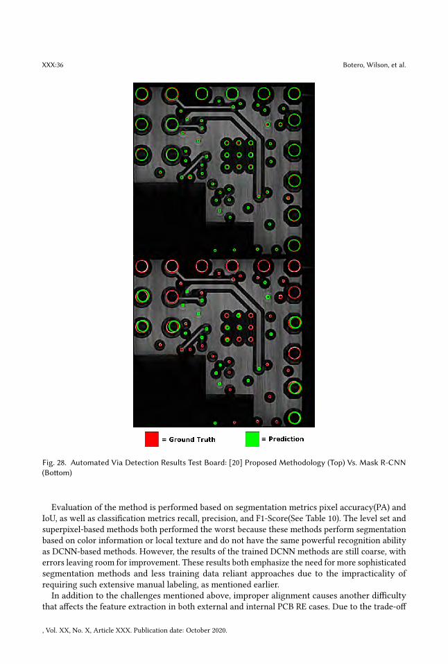
XXX:36 Botero, Wilson, et al.
Fig. 28. Automated Via Detection Results Test Board: [20] Proposed Methodology (Top) Vs. Mask R-CNN(Bottom)
Evaluation of the method is performed based on segmentation metrics pixel accuracy(PA) andIoU, as well as classification metrics recall, precision, and F1-Score(See Table 10). The level set andsuperpixel-based methods both performed the worst because these methods perform segmentationbased on color information or local texture and do not have the same powerful recognition abilityas DCNN-based methods. However, the results of the trained DCNN methods are still coarse, witherrors leaving room for improvement. These results both emphasize the need for more sophisticatedsegmentation methods and less training data reliant approaches due to the impracticality ofrequiring such extensive manual labeling, as mentioned earlier.In addition to the challenges mentioned above, improper alignment causes another difficulty
that affects the feature extraction in both external and internal PCB RE cases. Due to the trade-off
, Vol. XX, No. X, Article XXX. Publication date: October 2020.

Hardware Trust and Assurance through Reverse Engineering:XXX:37
Table 10. Trace wire segmentation performance comparison [150]
Trace Detection Performance ComparisonMethod PA IoU Recall Precision F1-Score
Levelset [213] .8246 .5743 .4585 .3123 .3715Superpixel [90] .8074 .6534 .4792 .6064 .5353DCNN-GC [150] .9002 .8463 .8629 .8655 .8642
Fig. 29. Misaligned external PCB image
Fig. 30. Misaligned Xilinx Spartan board X-Ray CT slice
between details included in the features and the size of the features in external PCB imaging,some components cannot be captured completely in a single image, and thus we require aligned(stitched) images to extract the features. Although this matter has been dealt with by using theCharge-Coupled Device (CCD) camera and SEM imaging [24, 126], the lighting condition and thenumber of assembled components can still lead to the stitching errors (see Figure 29) in externalPCB images. The same issue happens in the internal PCB RE. The aliasing effect in the slices thatmake up the 3D board sample (see Figure 18) is a byproduct of misalignment. This leads eventually
, Vol. XX, No. X, Article XXX. Publication date: October 2020.

XXX:38 Botero, Wilson, et al.
Fig. 31. Layer Identification Results [19]
to having the layers containing various amounts of feature information that may associate with asingle layer or an adjacent one. Additionally, misalignment can also lead to another issue – missinginformation (see Figure 30 where red dashed regions show areas of missing information). Therefore,it is important to not only be able to detect these features at each slice during feature extraction,but also address misalignment beforehand in order to localize and correspond the features to theircorrect layer.
There has been early work to address the misalignment/aliasing challenge [18] in internal PCBRE, as well as identifying what slices belong to what layers of a volumetric PCB stack dependingon varying levels of a priori information [18, 19]. First, [18] provided an algorithm that enablesfully automated unsupervised 3D-stack alignment via iterative robust regression and registrationbased on the image gradient direction of the volumetric PCB stack. With these slices now alignedand registered, the data better facilitates slice-to-layer identification, which is key for internal PCBRE and determining which features correspond to which layers. [18] then leverages the similarityof aligned adjacent slices in an X-ray CT imaged volumetric stack by using K-means clustering,in combination with exponentially windowed cross correlation, to identify what slices belong towhat layers in an automated unsupervised manner, where the reverse engineer in practice has noreference design information.In [19] the authors then explore the effectiveness of automated slice-to-layer identification
under the assumption that the RE has reference design information available either in the form ofCAD software provided digital images of the layers present in the board, or their X-ray CT imagedequivalent. However, the challenge for this task is that the provided reference design knowledgemaynot always be of the same imaging modality as the X-ray CT data. To address this heterogeneousimage comparison challenge, the authors employed a feature based approach utilizing the spatialpyramid bag of visual words model [111] in an iterative manner with various weighting schemesand then compare their results not only against the unsupervised methodology [18] but also againstnaive pixel intensity based approaches. Table 11 summarizes the results across the different methodsfrom a classification perspective as well as image quality assessment due to the desired result forsubsequent RE stages being a fused singular image of the slices composing a layer.
In particular, in [18], the importance of having domain knowledge of the X-Ray CT process forsolving the slice-to-layer correspondence issue is highlighted. Specifically, slice location informationis critical for unsupervised slice-to-layer identification due to the similarity of adjacent slices inan X-ray CT imaged volumetric stack. Unsupervised approaches tested in [18] that did not utilizeexponential windowing to emphasize location did not report a single instance of an F1-Score
, Vol. XX, No. X, Article XXX. Publication date: October 2020.
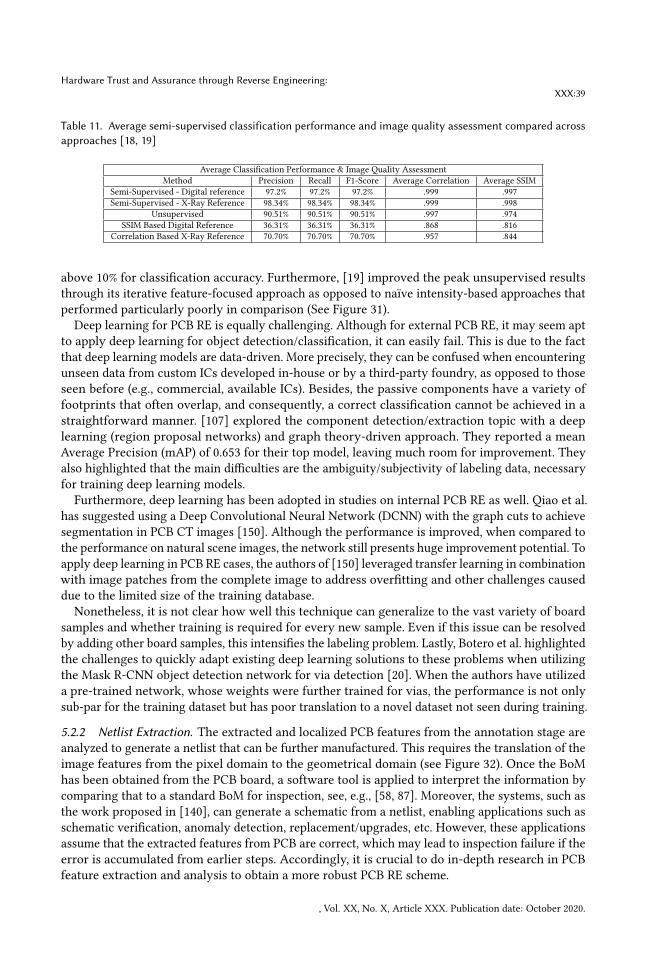
Hardware Trust and Assurance through Reverse Engineering:XXX:39
Table 11. Average semi-supervised classification performance and image quality assessment compared acrossapproaches [18, 19]
Average Classification Performance & Image Quality AssessmentMethod Precision Recall F1-Score Average Correlation Average SSIM
Semi-Supervised - Digital reference 97.2% 97.2% 97.2% .999 .997Semi-Supervised - X-Ray Reference 98.34% 98.34% 98.34% .999 .998
Unsupervised 90.51% 90.51% 90.51% .997 .974SSIM Based Digital Reference 36.31% 36.31% 36.31% .868 .816
Correlation Based X-Ray Reference 70.70% 70.70% 70.70% .957 .844
above 10% for classification accuracy. Furthermore, [19] improved the peak unsupervised resultsthrough its iterative feature-focused approach as opposed to naïve intensity-based approaches thatperformed particularly poorly in comparison (See Figure 31).
Deep learning for PCB RE is equally challenging. Although for external PCB RE, it may seem aptto apply deep learning for object detection/classification, it can easily fail. This is due to the factthat deep learning models are data-driven. More precisely, they can be confused when encounteringunseen data from custom ICs developed in-house or by a third-party foundry, as opposed to thoseseen before (e.g., commercial, available ICs). Besides, the passive components have a variety offootprints that often overlap, and consequently, a correct classification cannot be achieved in astraightforward manner. [107] explored the component detection/extraction topic with a deeplearning (region proposal networks) and graph theory-driven approach. They reported a meanAverage Precision (mAP) of 0.653 for their top model, leaving much room for improvement. Theyalso highlighted that the main difficulties are the ambiguity/subjectivity of labeling data, necessaryfor training deep learning models.Furthermore, deep learning has been adopted in studies on internal PCB RE as well. Qiao et al.
has suggested using a Deep Convolutional Neural Network (DCNN) with the graph cuts to achievesegmentation in PCB CT images [150]. Although the performance is improved, when compared tothe performance on natural scene images, the network still presents huge improvement potential. Toapply deep learning in PCB RE cases, the authors of [150] leveraged transfer learning in combinationwith image patches from the complete image to address overfitting and other challenges causeddue to the limited size of the training database.Nonetheless, it is not clear how well this technique can generalize to the vast variety of board
samples and whether training is required for every new sample. Even if this issue can be resolvedby adding other board samples, this intensifies the labeling problem. Lastly, Botero et al. highlightedthe challenges to quickly adapt existing deep learning solutions to these problems when utilizingthe Mask R-CNN object detection network for via detection [20]. When the authors have utilizeda pre-trained network, whose weights were further trained for vias, the performance is not onlysub-par for the training dataset but has poor translation to a novel dataset not seen during training.
5.2.2 Netlist Extraction. The extracted and localized PCB features from the annotation stage areanalyzed to generate a netlist that can be further manufactured. This requires the translation of theimage features from the pixel domain to the geometrical domain (see Figure 32). Once the BoMhas been obtained from the PCB board, a software tool is applied to interpret the information bycomparing that to a standard BoM for inspection, see, e.g., [58, 87]. Moreover, the systems, such asthe work proposed in [140], can generate a schematic from a netlist, enabling applications such asschematic verification, anomaly detection, replacement/upgrades, etc. However, these applicationsassume that the extracted features from PCB are correct, which may lead to inspection failure if theerror is accumulated from earlier steps. Accordingly, it is crucial to do in-depth research in PCBfeature extraction and analysis to obtain a more robust PCB RE scheme.
, Vol. XX, No. X, Article XXX. Publication date: October 2020.

XXX:40 Botero, Wilson, et al.
Anti-PCB RE approaches are focused onmaking RE at the PCB-level prohibitively more expensiveand time-consuming than it is worth. This is done in a variety of ways, with varying complexities.The work presented in [133] focuses on the design and implementation of a few passive components,more unmarked ICs, using custom silicon, and/or having cases of missing silkscreens. Thesemethodshave low to moderate overhead with regards to design cost and manufacturing impact. However,they only increase RE costs by a small margin. Instead, by utilizing a multi-layer board, blind andburied vias, and/or routing signals for the inner layers, the RE costs can be significantly raised [151].Additionally, obfuscation can also be utilized for anti-RE of PCBs [72], similar to its applicationfor anti-RE at the IC level. Components referred to as permutation blocks can be used to hide theinterconnects among the circuit components on PCBs.Existing research on how to counter X-Ray-enabled RE focuses on inserting X-Ray detecting
sensors and using specific materials. X-Ray detecting sensors are devices embedded in a PCB design,being sensitive to X-Rays and react once a predetermined length of exposure to X-Rays has occurred.Afterward, the sensors signal a destructive measure to take place on the board to delay the REprocess or simply act as an indicator that RE has taken place. Furthermore, high-density materialswith high X-Ray attenuation factors, such as Zirconia powder, could be used throughout a board toreduce the quality of the X-Ray images. Using this material in a specific pattern throughout severallayers can drastically affect the X-Ray transmission through a PCB, resulting in a much lowersignal-to-noise ratio and low-quality 3D reconstruction of the PCB sample [6]. The combinationof the anti-RE techniques for external RE with these techniques for internal RE could provide aholistic solution to protect the system from RE.
6 FUTURE RESEARCH DIRECTIONSUp until this point, we have described the main building blocks of a typical RE framework (see Figure1(a)), put together to meet the main requirements of an automated approach. Moreover, numerousstudies introducing and employing various ML and image analysis techniques are reviewed, wherethe most prominent ones used at various stages of the RE workflow are summarized in Table 12. Inthis respect, the advantages and disadvantages of those algorithms are highlighted and assessedwith regard to their applications and performance. In fact, the end goal of the entire RE process is toleverage the advantages offered by image analysis and machine learning and eventually perform REin an automated manner. In addition to obvious benefits, namely the reduction in manpower andcosts, automated RE enables a variety of applications, which can further exploit the informationprovided by the RE. In this context, the following topics and possible future research directions aresuggested.
(1) Enhanced Hardware Assurance:With automated RE achieved at both of the IC and PCB-levels,it can allow for enhanced levels of assurance, when validating or verifying a design. Thedetection of defects, design alterations, or IP infringement can be improved to a pixel-levelaccuracy and performed more efficiently. However, it is not known whether a substantial im-provement over the state-of-the-art techniques can be achieved through these advancements.This needs to be explored in future work in this area.
(2) Qualitative Evaluation of Reverse Engineering: While each block in the RE framework isnecessary to achieve a high level of automation, no method has been yet developed in theliterature that can evaluate the performance of the RE process at each stage of the framework,let alone the whole process. Defining metrics and criteria for the quality assessment ofRE can also provide the ability to explore not only the trade-offs between the quality atvarious stages, but also their impact on the entire RE process. This can, of course, facilitate
, Vol. XX, No. X, Article XXX. Publication date: October 2020.

Hardware Trust and Assurance through Reverse Engineering:XXX:41
Fig. 32. Via and trace vectorized features
possible improvements in efficiency in terms of time, complexity, and required computationalresources.
(3) Benchmarking: Besides the above point regarding the performance analysis of the algorithms,providing a quantitative comparison between their performance is further challenging. Thisis a direct consequence of the lack of a comprehensive benchmark dataset that can be used tocompare the algorithms. Such a database cannot be built easily due to the complex undertakinginvolved in preparing instances. This problem can be even more severe for deep learningalgorithms, as discussed below.
(4) Reverse Engineering Optimization via Deep Learning: Due to the lack of a sufficiently largeamount of data as well as the variations in data collected across designs, the requirements ofeffective deep learning models cannot be fulfilled. However, after conducting an RE process,certain stages, e.g., de-noising, via/trace feature extraction, etc., can be optimized via deeplearning. In this regard, we can employ synthetic data generation and augmentation, alongwith using previously extracted RE data as ground truth. This can indeed help to make thosestages more time-efficient, when conventional deep neural networks or convolutional neuralnetworks are applied. As this has not been thoroughly explored, the actual extent of suchimprovement is not known.
, Vol. XX, No. X, Article XXX. Publication date: October 2020.

XXX:42 Botero, Wilson, et al.
(5) Functional vs. Design Equivalence: Our earlier discussion of image analysis- and machinelearning-enabled RE has focused on developing a method to reproduce an IC or, similarly, aPCB as close to the original one as possible. However, there are often scenarios, where only afunctionally-equivalent reproduction is necessary rather than a precise design reproduction.As an example, we can refer to an automated generation of a new design built upon somearbitrary standard cells, but with the same functionally as the original one with the foundry-specific standard cells. For PCBs, this can be even more straightforward: producing a PCB,whose connectivity is maintained, but not its specifications, e.g., the trace/via width ordistances. Future research should not only focus on such cases, but also go beyond those byconsidering a broader range of equivalence options, instead of solely functional and designequivalence.
(6) Missing Data Reconstruction: Regardless of the modality, one has to deal with the noise inthe collected data. The impact of the noise can range from missing regions of the informationin a de-processed IC to missing artifacts on a PCB after performing the X-Ray CT. If RE canbe automated, it is reasonable to acquire a large amount of data to model particular noisecharacteristics observed during image acquisition. These models could then be employed tocorrect noisy data and even reconstruct missing data. While this is well studied in machinelearning- and image analysis-related literature, the feasibility and extent to which this can beachieved for IC and PCB RE have yet to be explored.
(7) Compression Algorithms for RE: Another interesting aspect of RE to be taken into accountin future work is that the minimum amount of information or data required for a successfulreconstruction of images should be collected and stored on a computer system. In addition tospeeding up the process of image acquisition, this has the added benefit in terms of spacecomplexity. Unlike common image compression algorithms that attempt to attain the highestpossible level of visual quality, new algorithms can be designed or adapted to accuratelyreconstruct the required features, which leads to a saving of the storage and processingresources.
(8) Cross-Modality Comparison and Evaluation: One of the biggest challenges facing us, whenevaluating the performance of an RE process, is to compare results across different modalities.Irrespective of the modality (i.e., SEM, Optical, X-Ray CT), the final output of the RE frame-work should be compared to either a software-provided golden design in a digital format ora PCB schematic. This also requires the exploration of new techniques that can incorporatevarious factors including different characteristics of the data, the impact of the noise, andvariations across the modalities.
(9) Countermeasures against Advanced RE-based Attacks: While the techniques mentionedin earlier sections are useful to stop an attacker enjoying the advantages of the current,commonly applied RE framework, this cannot be guaranteed in the future. In particular,to deal with adversaries that can conduct RE, enhanced through the adoption of machinelearning and image analysis algorithms, the designer has to predict the risk of such emergingattacks. To this end, it is crucial to estimate the amount of effort that the attacker has toput and design measures to make the RE process significantly less effective and inefficient.Unfortunately, such estimations cannot be carried out in a straightforward manner. Therefore,new research directions regarding counter automated-RE development can be of great interestfor researchers from government, industry, and academia.
, Vol. XX, No. X, Article XXX. Publication date: October 2020.

Hardware Trust and Assurance through Reverse Engineering:XXX:43
T able12.Su
mmaryof
themetho
dsap
pliedin
thecontextof
RE
Article
Main
Contrib
u-tio
nScop
eAlgorith
ms
Features
Used
Metric
sEv
aluatio
nMetho
dSh
ortcom
ings
forR
E
[108]
Segm
entatio
nIC
Edge
detection
Metallayers
NA
Visual
Opticalmicroscop
eim
ages
[35]
Segm
entatio
nIC
K -means
andSV
MCo
ntact
and
Metal
layers
F-score
Grou
ndtru
thOnlyapplicable
tovias
and
metalconn
ectio
ns[34,36]
Segm
entatio
nIC
K -means,Fu
zzy
C-Means,
SVM
Polysilicon
andCo
n-tactlayers
Interse ctio
nover
Union
(IoU),
pixel
accuracy
Grou
ndtru
thRe
quire
spo
pulatio
nof
shapelib
rary
[51,
130,
195]
Segm
entatio
nIC
Spatialand
frequ
ency
do-
mainfilterin
gCo
ntact
and
Metal
layers
NA
Visual
Naive
applications
ofim
age
processin
g[82]
Segm
entatio
nIC
DCN
NCo
ntact
and
Metal
layers
False
Positive,
Nega-
tiveandsemantic
er-
rors
Grou
ndtru
thNe eds
500,0
00labelledsam-
ples
totra
in
[44]
Extra
ction
ofStandard
Cell
Library
ICNormalized
cross-
correlation
Dop
inglayer
NA
Grou
ndtru
thDesignedforp
artia
lRE
[207]
Extra
ction
ofStandard
Cell
Library
ICRu
lebased
Contact layer
NA
AES
desig
nswith
grou
ndtru
thOver/Un
der-segm
ented
cells
[215, 216]
Localizing
stan-
dard
cells
ICT emplateMatching
Cond
uctiv
elayers
NA
NA
Uses
approxim
ation
tospeedup
celllocalization
[3,96]
Netlist
genera-
tion
ICTemplateMatching
Alllayers
NA
NA
Requ
ires
standard
cell
li-brary
[152]
Netlist
genera-
tion
ICX G
Boost
Alllayers
with
pixel
intensity
,gradient
andHumom
ents
NA
Grou
ndtru
thNe eds
tobe
finetunedfor
diffe
rent
ICs
[8,
118,
120,182]
High-level
de-
scrip
tion
ofsub-circuits
ICTo
pologicala
nalyses,fuzzy
structuralsim
ilarity
Netlist
NA
Grou
ndtru
thUs
essim
ilarity
betw
een
know
nlib
rarie
sof
func-
tionalblocks
togenerate
descrip
tion
[168,189,
193]
Develop
mentof
toolsfor
REIC
NA
Alllayers
NA
NA
Assumes
availability
ofsomeinform
ation,
e.g.,the
standard
celllib
rary
[172, 196]
ICTrojan
detec-
tion
onactiv
elayer
ICRu
lebased
Shapeof
logicc
ells
NA
Designed
on-chip
training
data
Semi-d
estru
ctive,need
man-
ualp
olish
ing
Contin
uedon
next
page
, Vol. XX, No. X, Article XXX. Publication date: October 2020.

XXX:44 Botero, Wilson, et al.
Article
Main
Contrib
u-tio
nScop
eAlgorith
ms
Features
Used
Metric
sEv
aluatio
nMetho
dSh
ortcom
ings
forR
E
[7]
Non
-Destru
ctive
Imaging
and
Netlist
Extra
c-tio
n
PCB
X -Ra
yCT
ImagingandIm
-ageSegm
entatio
nX -Ra
yCT
Slices
NA
Dataset
with
De-Po
pulated
Board
V ery
manualand
parame-
terdepend
entim
age
pro-
cessing
[31,32,50,
94,
115,
185,191]
PCB
Defect
Detectio
nand
QualityCo
ntrol
PCB
Image
Subtraction[31,32,
50,9
4,115,
191]
andDeep
Learning
[185]
PCBLayerImages
Precision
and
F-Score
Golden
PCBLayerImage
Requ
iresb
arebo
ardgo
lden
layerimages
[119]
T ext
Recogn
i-tio
non
PCB
Surfa
ce
PCB
Optical
CharacterRe
cogn
i-tio
n,Binariz
ation,andBa
ck-
grou
ndEstim
ation
Boardsurfa
ceim
age
F-Score,
Precision
,andRe
call
Compar ed
against
freely
available
OCR
engines
OCR
AD,
Tesseract-O
CR,
Cuneifo
rm-linu
x,and
GOCR
ongrou
ndtru
th
Sub-op
timalaccuracy
[150]
T racesegm
enta-
tion
PCB
DCN
Nand
Graph
Cuts-
based
Semantic
Segm
enta-
tion
PCBCT
Images
Pixelaccuracy,IoU,
F1-Score,
Precision
,Re
call
50PC
BCT
testim
ages
Dealin
gwith
the
noise
,reliance
ontra
ining
data,
and
varia
nce
across
de-
signs/im
aging.
, Vol. XX, No. X, Article XXX. Publication date: October 2020.

Hardware Trust and Assurance through Reverse Engineering:XXX:45
7 CONCLUSIONIn this tutorial, we have comprehensively discussed the challenges associated with RE of ICs andPCBs. It has been observed that for hardware trust and assurance, even though existing, well-knownmethods (e.g., functional analysis) can be considered useful, the challenges of such methods rise inproportion to the complexity of the IC. The aim of the design in the semiconductor industry is tomove towards a higher performance and efficiency and the upward trend of complexity can remainintact for the years to come. Hence, the need for effective RE becomes greater than ever before.From the imaging perspective, it has been noted that the primary challenge to be faced by
an effective RE-based method is the lack of understanding of the nature of the noise in imagingmodalities used for RE, e.g., SEM and CEM. This can be augmented by the techniques used topre-process the IC for imaging, such as decapsulation and delayering. Furthermore, the time spentto acquire high-quality images with a reduced noise level makes RE infeasible for ICs employingtoday’s technology nodes.Our overview of machine learning going hand in hand with RE has demonstrated the need for
quantifying the amount of useful information in each layer. In addition, the effect of counter-RE onmachine learning-enabled techniques has been further investigated. Finally, the high variability offeatures between the layers of different ICs and the lack of high-quality datasets addressing thisissue have been observed and regarded as an obstacle to the employment of deep learning for RE.
While relevant literature regarding PCB RE is not rich, there has been a clear interest in takingadvantage of image analysis and machine learning algorithms for quality assurance in PCB man-ufacturing processes. These approaches typically involve image subtraction or (to some extent)building models for detecting defect/anomaly during the manufacturing process. Nevertheless,algorithms implemented for these purposes are not sufficient as they cannot resolve challenges withthe external or internal PCB RE. As a prime example, external PCB RE requires robust, illumination-invariant algorithms to be developed, which ensures effective, high-quality component extractionand analysis. In addition to the intensity inhomogeneity, algorithms designed to deal with internalPCB RE must also be robust to blurring artifacts caused by the X-ray, high-z materials, and aliasingfrom neighboring layers. Furthermore, due to the wide variety of designs across technologies andthe lack of representative datasets, a generalization of the results can pose a serious problem to RE.Finally, we believe that this tutorial paves the way for the necessary broad discussion on the
above issues and how hardware trust and assurance can benefit greatly from RE.
ACKNOWLEDGMENTSThis paper is based upon work supported by Cisco, AFOSR under award No. FA9550-14-1-0351,National Science Foundation under grant No.1821780, and National Science Foundation GraduateResearch Fellowship under Grant Nos. 1315138 and 1842473.
REFERENCES[1] Jason Abt and Chris Pawlowicz. 2012. Circuit Analysis Techniques: Delayering and Circuit Vision. http://www.
techinsights.com/[Accessed: Feb. 27, 2021].[2] Nitin Aggarwal and W Clem Karl. 2006. Line detection in images through regularized Hough transform. IEEE
transactions on image processing 15, 3 (2006), 582–591.[3] Haroon Ahmed, Simon Blythe, and Beatrice Fraboni. 1993. Integrated circuit structure analysis. US Patent 5,191,213.[4] C. Albrecht. 2005. Iwls 2005 benchmarks. http://www.iwls.org [Accessed Feb. 27, 2021].[5] N. Arazm, A. Sahab, and M. F. Kazemi. 2017. Noise reduction of SEM images using adaptive Wiener filter. In 2017
IEEE International Conference on Cybernetics and Computational Intelligence (CyberneticsCom). 50–55.[6] Navid Asadizanjani, Sina Shahbazmohamadi, Mark Tehranipoor, and Domenic Forte. 2015. Non-destructive pcb
reverse engineering using x-ray micro computed tomography. In 41st International symposium for testing and failureanalysis, ASM. 1–5.
, Vol. XX, No. X, Article XXX. Publication date: October 2020.

XXX:46 Botero, Wilson, et al.
[7] Navid Asadizanjani, Mark Tehranipoor, and Domenic Forte. 2017. PCB reverse engineering using nondestructiveX-ray tomography and advanced image processing. IEEE Transactions on Components, Packaging and ManufacturingTechnology 7, 2 (2017), 292–299.
[8] Johanna Baehr, Alessandro Bernardini, Georg Sigl, and Ulf Schlichtmann. 2019. Machine learning and structuralcharacteristics for reverse engineering. In Proceedings of the 24th Asia and South Pacific Design Automation Conference.ACM, 96–103.
[9] Johanna Baehr, Alessandro Bernardini, Georg Sigl, and Ulf Schlichtmann. 2020. Machine learning and structuralcharacteristics for reverse engineering. Integration 72 (2020), 1–12.
[10] Chongxi Bao, Domenic Forte, and Ankur Srivastava. 2014. On application of one-class SVM to reverse engineering-based hardware Trojan detection. In Fifteenth International Symposium on Quality Electronic Design. IEEE, 47–54.
[11] Chongxi Bao, Domenic Forte, and Ankur Srivastava. 2015. On reverse engineering-based hardware Trojan detection.IEEE Transactions on Computer-Aided Design of Integrated Circuits and Systems 35, 1 (2015), 49–57.
[12] Chongxi Bao, Domenic Forte, and Ankur Srivastava. 2016. On reverse engineering-based hardware Trojan detection.IEEE Transactions on Computer-Aided Design of Integrated Circuits and Systems 35, 1 (2016), 49–57.
[13] Chongxi Bao, Yang Xie, Yuntao Liu, and Ankur Srivastava. 2018. Reverse engineering-based hardware trojan detection.In The Hardware Trojan War. Springer, 269–288.
[14] Christopher F Batten. 2000. Autofocusing and astigmatism correction in the scanning electron microscope. Mphillthesis, University of Cambridge (2000).
[15] Csaba Benedek, Olivér Krammer,Mihály Janóczki, and László Jakab. 2012. Solder paste scooping detection bymultilevelvisual inspection of printed circuit boards. IEEE Transactions on Industrial Electronics 60, 6 (2012), 2318–2331.
[16] Simon Blythe, Beatrice Fraboni, Sanjay Lall, Haroon Ahmed, and Ugo de Riu. 1993. Layout reconstruction of complexsilicon chips. IEEE journal of solid-state circuits 28, 2 (1993), 138–145.
[17] F Edward Boas and Dominik Fleischmann. 2012. CT artifacts: causes and reduction techniques. Imaging in Medicine4, 2 (2012), 229–240.
[18] Ulbert J. Botero, Navid Asadizanjani, Damon L. Woodard, and Domenic Forte. 2020. A Framework for AutomatedAlignment and Layer Identification of X-Ray Tomography Imaged PCBs. In GOMACTech. San Francisco.
[19] Ulbert J. Botero, Fatemeh Ganji, Navid Asadizanjani, Damon Woodard, and Domenic Forte. 2020. Semi-SupervisedAutomated Layer Identification of X-ray Tomography Imaged PCBs. In accepted for presentation at InternationalConference on PHYSICAL ASSURANCE and INSPECTION of ELECTRONICS (PAINE), 2020. IEEE.
[20] Ulbert J. Botero, David Koblah, Daniel Capecci, Fatemeh Ganji, Navid Asadizanjani, Damon Woodard, and DomenicForte. 2020. Automated Via Detection for PCB Reverse Engineering. In accepted for presentation at InternationalSymposium for Testing and Failure Analysis, 2020. ASM.
[21] Ulbert J Botero, Mark M Tehranipoor, and Domenic Forte. 2019. Upgrade/Downgrade: Efficient and Secure LegacyElectronic System Replacement. IEEE Design & Test 36, 1 (2019), 14–22.
[22] Nikolaos G Bourbakis, A Mogzadeh, S Mertoguno, and Cris Koutsougeras. 2002. A knowledge-based expert system forautomatic visual VLSI reverse-engineering: VLSI layout version. IEEE Transactions on Systems, Man, and Cybernetics-Part A: Systems and Humans 32, 3 (2002), 428–436.
[23] David C Bowman. 2018. Image Stitching and Matching Tool in the Automated Iterative Reverse Engineer (AIRE)Integrated Circuit Analysis Suite. (2018).
[24] Matthew Brown and David G Lowe. 2007. Automatic panoramic image stitching using invariant features. Internationaljournal of computer vision 74, 1 (2007), 59–73.
[25] Burçin Cakır and Sharad Malik. 2015. Hardware Trojan detection for gate-level ICs using signal correlation basedclustering. In 2015 Design, Automation & Test in Europe Conference & Exhibition (DATE). IEEE, 471–476.
[26] Burcin Cakir and Sharad Malik. 2018. Reverse engineering digital ICs through geometric embedding of circuit graphs.ACM Transactions on Design Automation of Electronic Systems (TODAES) 23, 4 (2018), 1–19.
[27] Stephan De Castro, Jean-Max Dutertre, Bruno Rouzeyre, Giorgio Di Natale, and Marie-Lise Flottes. 2016. Frontsideversus backside laser injection: a comparative study. ACM Journal on Emerging Technologies in Computing Systems(JETC) 13, 1 (2016), 1–15.
[28] Rajat Subhra Chakraborty, Francis Wolff, Somnath Paul, Christos Papachristou, and Swarup Bhunia. 2009. MERO:A statistical approach for hardware Trojan detection. In International Workshop on Cryptographic Hardware andEmbedded Systems. Springer, 396–410.
[29] Wei-Hsin Chang, Shuenn-Der Tzeng, and Chen-Yi Lee. 2001. A novel subcircuit extraction algorithm by recursiveidentification scheme. In ISCAS 2001. The 2001 IEEE International Symposium on Circuits and Systems (Cat. No.01CH37196), Vol. 5. IEEE, 491–494.
[30] Narendra Chaudhary, Serap A Savari, and Sai S Yeddulapalli. 2019. Line roughness estimation and Poisson denoisingin scanning electron microscope images using deep learning. Journal of Micro/Nanolithography, MEMS, and MOEMS18, 2 (2019), 024001.
, Vol. XX, No. X, Article XXX. Publication date: October 2020.

Hardware Trust and Assurance through Reverse Engineering:XXX:47
[31] Vikas Chaudhary, Ishan R Dave, and Kishor P Upla. 2017. Automatic visual inspection of printed circuit board fordefect detection and classification. In 2017 International Conference on Wireless Communications, Signal Processing andNetworking (WiSPNET). IEEE, 732–737.
[32] Rasika R Chavan, Swati A Chavan, Gautami D Dokhe, Mayuri B Wagh, and Archana S Vaidya. 2016. Quality Controlof PCB using Image Processing. International Journal of Computer Applications 975 (2016), 8887.
[33] Jinghui Chen, Chen Dong, Fan Zhang, and Guorong He. 2019. A Hardware-Trojans Detection Approach Based oneXtreme Gradient Boosting. In 2019 IEEE 2nd International Conference on Computer and Communication EngineeringTechnology (CCET). IEEE, 69–73.
[34] Deruo Cheng, Yiqiong Shi, Bah-Hwee Gwee, Kar-Ann Toh, and Tong Lin. 2018. A Hierarchical Multiclassifier Systemfor Automated Analysis of Delayered IC Images. IEEE Intelligent Systems 34, 2 (2018), 36–43.
[35] Deruo Cheng, Yiqiong Shi, Tong Lin, Bah-Hwee Gwee, and Kar-Ann Toh. 2018. Hybrid K-Means Clustering andSupport Vector Machine Method for via and Metal Line Detections in Delayered IC Images. IEEE Transactions onCircuits and Systems II: Express Briefs 65, 12 (2018), 1849–1853.
[36] Deruo Cheng, Yiqiong Shi, Tong Lin, Bah-Hwee Gwee, and Kar-Ann Toh. 2019. Global Template Projection andMatching Method for Training-Free Analysis of Delayered IC Images. In 2019 IEEE International Symposium onCircuits and Systems (ISCAS). IEEE, 1–5.
[37] D Cheremisinov and L Cheremisinova. 2020. Subcircuit Pattern Recognition in Transistor Level Circuits. PatternRecognition and Image Analysis 30, 2 (2020), 160–169.
[38] Gregory H Chisholm, Steven T Eckmann, Christopher M Lain, and Robert L Veroff. 1999. Understanding integratedcircuits. IEEE Design & Test of Computers 16, 2 (1999), 26–37.
[39] Petr Cizmar, András E Vladár, Bin Ming, Michael T Postek, National Institute of Standards, and Technology. 2008.Simulated SEM images for resolution measurement. Scanning 30, 5 (2008), 381–391.
[40] Petr Cizmar, András E Vladár, and Michael T Postek. 2009. Optimization of accurate SEM imaging by use of artificialimages. In Scanning Microscopy 2009, Vol. 7378. International Society for Optics and Photonics, 737815.
[41] Ronald P Cocchi, James P Baukus, Lap Wai Chow, and Bryan J Wang. 2014. Circuit camouflage integration forhardware IP protection. In Proceedings of the 51st Annual Design Automation Conference. ACM, 1–5.
[42] Senate Armed Services Committee et al. 2012. Inquiry into counterfeit electronic parts in the department of defensesupply chain. Washington, DC: Author (2012).
[43] Vassilios Constantoudis, Vijaya-Kumar Murugesan Kuppuswamy, and Evangelos Gogolides. 2013. Effects of imagenoise on contact edge roughness and critical dimension uniformity measurement in synthesized scanning electronmicroscope images. Journal of Micro/Nanolithography, MEMS, and MOEMS 12, 1 (2013), 013005.
[44] Franck Courbon. 2019. Practical Partial Hardware Reverse Engineering Analysis. Journal of Hardware and SystemsSecurity (2019), 1–10.
[45] Franck Courbon, Philippe Loubet-Moundi, Jacques JA Fournier, and Assia Tria. 2015. A high efficiency hardwaretrojan detection technique based on fast SEM imaging. In Proceedings of the 2015 Design, Automation & Test in EuropeConference & Exhibition. EDA Consortium, 788–793.
[46] Franck Courbon, Philippe Loubet-Moundi, Jacques JA Fournier, and Assia Tria. 2015. SEMBA: A SEM based acquisitiontechnique for fast invasive Hardware Trojan detection. In 2015 European Conference on Circuit Theory and Design(ECCTD). IEEE, 1–4.
[47] Franck Courbon, Sergei Skorobogatov, and Christopher Woods. 2016. Reverse engineering flash EEPROM memoriesusing scanning electron microscopy. In International Conference on Smart Card Research and Advanced Applications.Springer, 57–72.
[48] Navneet Dalal and Bill Triggs. 2005. Histograms of oriented gradients for human detection. In 2005 IEEE computersociety conference on computer vision and pattern recognition (CVPR’05), Vol. 1. IEEE, 886–893.
[49] Piali Das, Olga Veksler, Vyacheslav Zavadsky, and Yuri Boykov. 2009. Semiautomatic segmentation with compactshape prior. Image and Vision Computing 27, 1-2 (2009), 206–219.
[50] NeelumDave, Vikas Tambade, Balaji Pandhare, and Suman Saurav. 2016. PCBDefect Detection Using Image ProcessingAnd Embedded System. International Research Journal of Engineering and Technology (IRJET) 3, 5 (2016), 1897–1901.
[51] Alexander Doudkin, Alexander Inyutin, and Maksim Vatkin. 2005. Objects identification on the color layout imagesof the integrated circuit layers. In 2005 IEEE Intelligent Data Acquisition and Advanced Computing Systems: Technologyand Applications. IEEE, 610–614.
[52] Roger Durà, Jofre Pallarès, Raúl Quijada, Xavier Formatjé, Salvador Hidalgo, and Francisco Serra-Graells. 2017. fastand robust Topology-Based logic gate identification for automated IC reverse engineering. In ISTFA 2017: the 43rdInternational Symposium for Testing and Failure Analysis. ASM International, 299.
[53] Mohamed El Massad, Siddharth Garg, and Mahesh V Tripunitara. 2015. Integrated Circuit (IC) Decamouflaging:Reverse Engineering Camouflaged ICs within Minutes.. In NDSS. 1–14.
, Vol. XX, No. X, Article XXX. Publication date: October 2020.

XXX:48 Botero, Wilson, et al.
[54] Rana Elnaggar and Krishnendu Chakrabarty. 2018. Machine Learning for Hardware Security: Opportunities andRisks. Journal of Electronic Testing 34, 2 (2018), 183–201.
[55] Luděk Frank. 2005. Noise in secondary electron emission: the low yield case. Journal of electron microscopy 54, 4(2005), 361–365.
[56] PDK Free. [n.d.]. 45nm open-access based PDK for the 45nm technology node.[57] Sean P Frigo, Zachary H Levine, and Nestor J Zaluzec. 2002. Submicron imaging of buried integrated circuit structures
using scanning confocal electron microscopy. Applied Physics Letters 81, 11 (2002), 2112–2114.[58] Chang-Wen Fu, Ge-Xin Zeng, De-Sheng Qiu, and Hui-Zhang Wang. 2007. System and method for generating a bill of
material file. US Patent App. 11/309,173.[59] Marc Fyrbiak. 2019. Constructive and destructive reverse engineering aspects of digital systems. Ph.D. Dissertation.
Ruhr University Bochum, Germany.[60] Marc Fyrbiak, Sebastian Strauß, Christian Kison, Sebastian Wallat, Malte Elson, Nikol Rummel, and Christof Paar.
2017. Hardware reverse engineering: Overview and open challenges. In 2017 IEEE 2nd International Verification andSecurity Workshop (IVSW). IEEE, 88–94.
[61] Vilas H Gaidhane, Yogesh V Hote, and Vijander Singh. 2018. An efficient similarity measure approach for PCB surfacedefect detection. Pattern Analysis and Applications 21, 1 (2018), 277–289.
[62] Sumyung Gang, Ndayishimiye Fabrice, and JoonJae Lee. 2020. Coresets for PCB Character Recognition based onDeep Learning. In 2020 International Conference on Artificial Intelligence in Information and Communication (ICAIIC).IEEE, 637–642.
[63] Swaroop Ghosh, Abhishek Basak, and Swarup Bhunia. 2014. How secure are printed circuit boards against trojanattacks? IEEE Design & Test 32, 2 (2014), 7–16.
[64] E Giannatou, G Papavieros, V Constantoudis, H Papageorgiou, and E Gogolides. 2019. Deep learning denoising ofSEM images towards noise-reduced LER measurements. Microelectronic Engineering 216 (2019), 111051.
[65] Richard Goldman, Karen Bartleson, TroyWood, Kevin Kranen, C Cao, Vazgen Melikyan, and Gayane Markosyan. 2009.Synopsys’ open educational design kit: capabilities, deployment and future. In 2009 IEEE International Conference onMicroelectronic Systems Education. IEEE, 20–24.
[66] R Goldman, K Bartleson, T Wood, K Kranen, V Melikyan, and E Babayan. 2013. 32/28nm educational design kit:Capabilities, deployment and future. In 2013 IEEE Asia Pacific Conference on Postgraduate Research in Microelectronicsand Electronics (PrimeAsia). IEEE, 284–288.
[67] Hector Gomez, Ckristian Duran, and Elkim Roa. 2018. Standard cell camouflage method to counter silicon reverseengineering. In 2018 IEEE International Conference on Consumer Electronics (ICCE). IEEE, 1–4.
[68] Hector Gomez, Ckristian Duran, and Elkim Roa. 2019. Defeating Silicon Reverse Engineering Using a Layout-LevelStandard Cell Camouflage. IEEE Transactions on Consumer Electronics 65, 1 (2019), 109–118.
[69] Joe Grand. 2014. Printed circuit board deconstruction techniques. In 8th {USENIX}Workshop on Offensive Technologies({WOOT} 14).
[70] Peng Gu, Dylan Stow, Prashansa Mukim, Shuangchen Li, and Yuan Xie. 2018. Cost-efficient 3D integration to hinderreverse engineering during and after manufacturing. In 2018 Asian Hardware Oriented Security and Trust Symposium(AsianHOST). IEEE, 74–79.
[71] Ujjwal Guin, Daniel DiMase, and Mohammad Tehranipoor. 2014. Counterfeit integrated circuits: detection, avoidance,and the challenges ahead. Journal of Electronic Testing 30, 1 (2014), 9–23.
[72] Zimu Guo, Mark Tehranipoor, Domenic Forte, and Jia Di. 2015. Investigation of obfuscation-based anti-reverseengineering for printed circuit boards. In 2015 52nd ACM/EDAC/IEEE Design Automation Conference (DAC). IEEE, 1–6.
[73] Mark C Hansen, Hakan Yalcin, and John P Hayes. 1999. Unveiling the ISCAS-85 benchmarks: A case study in reverseengineering. IEEE Design & Test of Computers 16, 3 (1999), 72–80.
[74] LR Harriott, A Wagner, and F Fritz. 1986. Integrated circuit repair using focused ion beam milling. Journal of VacuumScience & Technology B: Microelectronics Processing and Phenomena 4, 1 (1986), 181–184.
[75] Kento Hasegawa, Masaru Oya, Masao Yanagisawa, and Nozomu Togawa. 2016. Hardware Trojans classification forgate-level netlists based on machine learning. In 2016 IEEE 22nd International Symposium on On-Line Testing andRobust System Design (IOLTS). IEEE, 203–206.
[76] Kento Hasegawa, Masao Yanagisawa, and Nozomu Togawa. 2017. Hardware Trojans classification for gate-levelnetlists using multi-layer neural networks. In 2017 IEEE 23rd International Symposium on On-Line Testing and RobustSystem Design (IOLTS). IEEE, 227–232.
[77] Kento Hasegawa, Masao Yanagisawa, and Nozomu Togawa. 2017. Trojan-feature extraction at gate-level netlists andits application to hardware-Trojan detection using random forest classifier. In 2017 IEEE International Symposium onCircuits and Systems (ISCAS). IEEE, 1–4.
[78] Abdel-Aziz IM Hassanin, Fathi E Abd El-Samie, and Ghada M El Banby. 2019. A real-time approach for automaticdefect detection from PCBs based on SURF features and morphological operations. Multimedia Tools and Applications
, Vol. XX, No. X, Article XXX. Publication date: October 2020.

Hardware Trust and Assurance through Reverse Engineering:XXX:49
78, 24 (2019), 34437–34457.[79] KaimingHe, Georgia Gkioxari, Piotr Dollár, and Ross Girshick. 2017. Mask r-cnn. In Proceedings of the IEEE international
conference on computer vision. 2961–2969.[80] Kaiming He, Xiangyu Zhang, Shaoqing Ren, and Jian Sun. 2016. Identity mappings in deep residual networks. In
European conference on computer vision. Springer, 630–645.[81] Mirko Holler, Manuel Guizar-Sicairos, Esther HR Tsai, Roberto Dinapoli, Elisabeth Müller, Oliver Bunk, Jörg Raabe,
and Gabriel Aeppli. 2017. High-resolution non-destructive three-dimensional imaging of integrated circuits. Nature543, 7645 (2017), 402.
[82] Xuenong Hong, Deruo Cheng, Yiqiong Shi, Tong Lin, and Bah Hwee Gwee. 2018. Deep Learning for Automatic ICImage Analysis. In 2018 IEEE 23rd International Conference on Digital Signal Processing (DSP). IEEE, 1–5.
[83] Szu-Hao Huang and Ying-Cheng Pan. 2015. Automated visual inspection in the semiconductor industry: A survey.Computers in industry 66 (2015), 1–10.
[84] Xingjia Huang, Shengcong Zhu, Xuanyu Huang, Bing Su, Changping Ou, and Weili Zhou. 2015. Detection of platedthrough hole defects in printed circuit board with X-ray. In 2015 16th International Conference on Electronic PackagingTechnology (ICEPT). IEEE, 1296–1301.
[85] Taswar Iqbal and Kai-Dietrich Wolf. 2017. PCB Surface Fingerprints Based Counterfeit Detection of ElectronicDevices. Electronic Imaging 2017, 7 (2017), 144–149.
[86] Girishma Jain, Sandeep Raghuwanshi, and Gagan Vishwakarma. 2017. Hardware Trojan: Malware Detection UsingReverse Engineering and SVM. In International Conference on Intelligent Systems Design and Applications. Springer,530–539.
[87] Sang-Hun Jin. 2000. Method for transforming original bill-of-material for printed circuit board into standard bill-of-material. US Patent 6,041,268.
[88] Yier Jin, Nathan Kupp, and Yiorgos Makris. 2009. Experiences in hardware Trojan design and implementation. In2009 IEEE International Workshop on Hardware-Oriented Security and Trust. IEEE, 50–57.
[89] Yier Jin and Yiorgos Makris. 2008. Hardware Trojan detection using path delay fingerprint. In 2008 IEEE Internationalworkshop on hardware-oriented security and trust. IEEE, 51–57.
[90] Q Kai, C Jian, L Zhongguo, et al. 2016. Automatic printed circuit board wire detecting method of cone beam CTimage. Opt. Precis. Eng. 24, 2 (2016), 413–421.
[91] Heikki Kälviäinen, Petri Hirvonen, Lei Xu, and Erkki Oja. 1995. Probabilistic and non-probabilistic Hough transforms:overview and comparisons. Image and Vision Computing (1995). https://doi.org/10.1016/0262-8856(95)99713-B
[92] Nidal S Kamel and KS Sim. 2004. Image signal-to-noise ratio and noise variance estimation using autoregressivemodel. Scanning: The Journal of Scanning Microscopies 26, 6 (2004), 277–281.
[93] Michael Kass, Andrew Witkin, and Demetri Terzopoulos. 1988. Snakes: Active contour models. International journalof computer vision 1, 4 (1988), 321–331.
[94] Beant Kaur, Gurmeet Kaur, and Amandeep Kaur. 2014. Detection and classification of printed circuit board defectsusing image subtraction method. In 2014 Recent Advances in Engineering and Computational Sciences (RAECS). IEEE,1–5.
[95] Anna Lena Keller, Dirk Zeidler, and Thomas Kemen. 2014. High throughput data acquisition with a multi-beam SEM.In Scanning Microscopies 2014, Vol. 9236. International Society for Optics and Photonics, 92360B.
[96] K Yu Kenneth and C Neil Berglund. 1992. Automated system for extracting design and layout information from anintegrated circuit. US Patent 5,086,477.
[97] Shahrzad Keshavarz, Cunxi Yu, Samaneh Ghandali, Xiaolin Xu, and Daniel Holcomb. 2018. Survey on applications offormal methods in reverse engineering and intellectual property protection. Journal of Hardware and Systems Security2, 3 (2018), 214–224.
[98] Gyungtae Kim, Ming Ma, and Inhag Park. 2018. A fast and flexible software for IC reverse engineering. In 2018International Conference on Electronics, Information, and Communication (ICEIC). IEEE, 1–4.
[99] Jun-Oh Kim, Youn-Ae Lee, and Tae-Hyoung Park. 2012. Automatic extraction of component inspection regions fromPrinted Circuit Board. In 2012 IEEE/SICE International Symposium on System Integration (SII). IEEE, 871–876.
[100] Adam Kimura, Jon Scholl, James Schaffranek, Matthew Sutter, Andrew Elliott, Mike Strizich, and Glen David Via.2020. A Decomposition Workflow for Integrated Circuit Verification and Validation. Journal of Hardware and SystemsSecurity (2020), 1–10.
[101] Christian Kison. 2019. Advanced methods for hardware reverse engineering. Ph.D. Dissertation. Ruhr-UniversitätBochum.
[102] Johann Knechtel. 2020. Hardware Security for and beyond CMOS Technology: An Overview on Fundamentals,Applications, and Challenges. arXiv preprint arXiv:2001.08780 (2020).
[103] Johann Knechtel, Satwik Patnaik, and Ozgur Sinanoglu. 2019. Protect your chip design intellectual property: Anoverview. In Proceedings of the International Conference on Omni-Layer Intelligent Systems. 211–216.
, Vol. XX, No. X, Article XXX. Publication date: October 2020.
XXX:50 Botero, Wilson, et al.
[104] Stephen Kockentiedt, Klaus Tönnies, Erhardt Gierke, Nico Dziurowitz, Carmen Thim, and Sabine Plitzko. 2013.Poisson shot noise parameter estimation from a single scanning electron microscopy image. In Image Processing:Algorithms and Systems XI, Vol. 8655. International Society for Optics and Photonics, 86550N.
[105] Jin Won Koh, Gu Teak Hwang, Moon Seop Hyun, Jun-Mo Yang, and Jeoung Woo Kim. 2011. Semiconductor layerextraction techniques by SEM. In 18th IEEE International Symposium on the Physical and Failure Analysis of IntegratedCircuits (IPFA). IEEE, 1–3.
[106] Kishor Kunal, Tonmoy Dhar, Meghna Madhusudan, Jitesh Poojary, AK Sharma, Wenbin Xu, Steven M Burns, JiangHu, Ramesh Harjani, and Sachin S Sapatnekar. 2020. GANA: Graph Convolutional Network Based Automated NetlistAnnotation for Analog Circuits. Proc. DATE. ACM, New York, NY (2020).
[107] Chia-Wen Kuo, Jacob Ashmore, David Huggins, and Zsolt Kira. 2019. Data-efficient graph embedding learning forPCB component detection. In 2019 IEEE Winter Conference on Applications of Computer Vision (WACV). IEEE, 551–560.
[108] Dmitry Lagunovsky, Sergey Ablameyko, and M Kutas. 1998. Recognition of integrated circuit images in reverseengineering. In Proceedings. Fourteenth International Conference on Pattern Recognition (Cat. No. 98EX170), Vol. 2. IEEE,1640–1642.
[109] SH Lau, Andrei Tkachuk, Michael Feser, Hongtao Cui, Fred Duewer, Wenbing Yun, and David Vallet. 2006. Nondestructive failure analysis technique with a laboratory based 3D X-ray nanotomography system. In LSI TestingSymposium.
[110] A Lazar and Petru S Fodor. 2015. Sparsity based noise removal from low dose scanning electron microscopy images.In Computational Imaging XIII, Vol. 9401. International Society for Optics and Photonics, 940105.
[111] Svetlana Lazebnik, Cordelia Schmid, and Jean Ponce. 2006. Beyond bags of features: Spatial pyramid matching forrecognizing natural scene categories. Proceedings of the IEEE Computer Society Conference on Computer Vision andPattern Recognition 2 (2006), 2169–2178. https://doi.org/10.1109/CVPR.2006.68
[112] Yann LeCun, Fu Jie Huang, Leon Bottou, et al. 2004. Learning methods for generic object recognition with invarianceto pose and lighting. In CVPR (2). Citeseer, 97–104.
[113] Jang Hee Lee and Suk In Yoo. 2008. An effective image segmentation technique for the SEM image. In 2008 IEEEinternational conference on industrial technology. IEEE, 1–5.
[114] Myungjun Lee, Jason Cantone, Ji Xu, Lei Sun, and Ryoung-han Kim. 2014. Improving SEM image quality usingpixel super resolution technique. In Metrology, Inspection, and Process Control for Microlithography XXVIII, Vol. 9050.International Society for Optics and Photonics, 90500U.
[115] Fabiana R Leta, Flávio F Feliciano, and Flavius PR Martins. 2008. Computer vision system for printed circuit boardinspection. In ABCM Symposium Series in Mechatronics, Vol. 3. 623–632.
[116] Zachary H Levine, Andrew R Kalukin, Sean P Frigo, IanMcNulty, andMarkus Kuhn. 1999. Tomographic reconstructionof an integrated circuit interconnect. Applied physics letters 74, 1 (1999), 150–152.
[117] He Li, Qiang Liu, and Jiliang Zhang. 2016. A survey of hardware Trojan threat and defense. Integration 55 (2016),426–437.
[118] Wenchao Li, Adria Gascon, Pramod Subramanyan, Wei Yang Tan, Ashish Tiwari, Sharad Malik, Natarajan Shankar,and Sanjit A Seshia. 2013. Wordrev: Finding word-level structures in a sea of bit-level gates. In 2013 IEEE internationalsymposium on hardware-oriented security and trust (HOST). IEEE, 67–74.
[119] Wei Li, Stefan Neullens, Matthias Breier, Marcel Bosling, Thomas Pretz, and Dorit Merhof. 2014. Text recognition forinformation retrieval in images of printed circuit boards. In IECON 2014-40th Annual Conference of the IEEE IndustrialElectronics Society. IEEE, 3487–3493.
[120] Wenchao Li, Zach Wasson, and Sanjit A Seshia. 2012. Reverse engineering circuits using behavioral pattern mining.In 2012 IEEE international symposium on hardware-oriented security and trust. IEEE, 83–88.
[121] Konstantinos G Liakos, Georgios K Georgakilas, Serafeim Moustakidis, Patrik Karlsson, and Fotis C Plessas. 2019.Machine Learning for Hardware Trojan Detection: A Review. In 2019 Panhellenic Conference on Electronics & Telecom-munications (PACET). IEEE, 1–6.
[122] Tsung-Yi Lin, Michael Maire, Serge Belongie, James Hays, Pietro Perona, Deva Ramanan, Piotr Dollár, and C LawrenceZitnick. 2014. Microsoft coco: Common objects in context. In European conference on computer vision. Springer,740–755.
[123] Bernhard Lippmann, Niklas Unverricht, Aayush Singla, Matthias Ludwig, Michael Werner, Peter Egger, Anja Due-botzky, Helmut Graeb, Horst Gieser, Martin Rasche, et al. 2020. Verification of physical designs using an integratedreverse engineering flow for nanoscale technologies. Integration 71 (2020), 11–29.
[124] Bernhard Lippmann, Michael Werner, Niklas Unverricht, Aayush Singla, Peter Egger, Anja Dübotzky, Horst Gieser,Martin Rasche, Oliver Kellermann, and Helmut Graeb. 2019. Integrated flow for reverse engineering of nanoscaletechnologies. In Proceedings of the 24th Asia and South Pacific Design Automation Conference. ACM, 82–89.
[125] Xifeng Liu and Yuwei Hu. 2018. Automatic extraction of via in the CT image of PCB. In Ninth International Conferenceon Graphic and Image Processing (ICGIP 2017), Vol. 10615. International Society for Optics and Photonics, 106154J.
, Vol. XX, No. X, Article XXX. Publication date: October 2020.

Hardware Trust and Assurance through Reverse Engineering:XXX:51
[126] Bin Ma, Timo Zimmermann, Manfred Rohde, Simon Winkelbach, Feng He, Werner Lindenmaier, and Kurt EJ Dittmar.2007. Use of autostitch for automatic stitching of microscope images. Micron 38, 5 (2007), 492–499.
[127] Kaleel Mahmood, Pedro Latorre Carmona, Sina Shahbazmohamadi, Filiberto Pla, and Bahram Javidi. 2015. Real-timeautomated counterfeit integrated circuit detection using x-ray microscopy. Applied Optics 54, 13 (2015), D25–D32.
[128] Raman Maini and Himanshu Aggarwal. 2009. Study and comparison of various image edge detection techniques.International journal of image processing (IJIP) 3, 1 (2009), 1–11.
[129] DWMalone and RE Hummel. 1997. Electromigration in integrated circuits. Critical Reviews in Solid State and MaterialSciences 22, 3 (1997), 199–238.
[130] G Masalskis et al. 2008. Reverse engineering of CMOS integrated circuits. Elektronika ir elektrotechnika 88, 8 (2008),25–28.
[131] Erik Matlin, Motilal Agrawal, and David Stoker. 2014. Non-invasive recognition of poorly resolved integrated circuitelements. IEEE Transactions on Information Forensics and Security 9, 3 (2014), 354–363.
[132] Mohadeseh Mazhari and Reza PR Hasanzadeh. 2016. Suppression of noise in SEM images using weighted localhysteresis smoothing filter. Scanning 38, 6 (2016), 634–643.
[133] Ian McLoughlin. 2008. Secure embedded systems: The threat of reverse engineering. In 2008 14th IEEE InternationalConference on Parallel and Distributed Systems. IEEE, 729–736.
[134] Yoshihiro Midoh, Katsuyoshi Miura, Koji Nakamae, and Hiromu Fujioka. 2005. Statistical optimization of Canny edgedetector for measurement of fine line patterns in SEM image. Measurement Science and Technology 16, 2 (2005), 477.
[135] Madhav Moganti and Fikret Ercal. 1998. Segmentation of printed circuit board images into basic patterns. ComputerVision and Image Understanding 70, 1 (1998), 74–86.
[136] Samuel K. Moore. 2018. This Tech Would Have Spotted the Secret Chinese Chip in Seconds. https://spectrum.ieee.org/riskfactor/computing/hardware/this-tech-would-have-spotted-the-secret-chinese-chip-in-seconds
[137] Ryo Nakagaki, Yuji Takagi, and Koji Nakamae. 2010. Automatic recognition of circuit patterns on semiconductorwafers from multiple scanning electron microscope images. Measurement Science and Technology 21, 8 (2010), 085501.
[138] Seetharam Narasimhan, Xinmu Wang, Dongdong Du, Rajat Subhra Chakraborty, and Swarup Bhunia. 2011. TeSR: Arobust temporal self-referencing approach for hardware Trojan detection. In 2011 IEEE International Symposium onHardware-Oriented Security and Trust. IEEE, 71–74.
[139] Abdurrahman A Nasr and Mohamed Z Abdulmageed. 2017. An Efficient Reverse Engineering Hardware TrojanDetector Using Histogram of Oriented Gradients. Journal of Electronic Testing 33, 1 (2017), 93–105.
[140] B Naveen and KS Raghunathan. 1993. An automatic netlist-to-schematic generator. IEEE Design & Test of Computers10, 1 (1993), 36–41.
[141] Karsten Nohl, David Evans, Starbug Starbug, and Henryk Plötz. 2008. Reverse-Engineering a Cryptographic RFIDTag.. In USENIX security symposium, Vol. 28.
[142] OpenCores. 2012. OpenCores Oliscience. https://opencores.org/projects [Accessed: Feb. 27, 2021].[143] Ndubuisi G Orji, Mustafa Badaroglu, Bryan M Barnes, Carlos Beitia, Benjamin D Bunday, Umberto Celano, Regis J
Kline, Mark Neisser, Y Obeng, and AE Vladar. 2018. Metrology for the next generation of semiconductor devices.Nature electronics 1, 10 (2018), 532–547.
[144] OSU. [n.d.]. Oklahoma state university system on chip (soc) design flows. https://vlsiarch.ecen.okstate.edu/flow/[Accessed: Feb. 27, 2021].
[145] James Pawley and Heide Schatten. 2007. Biological low-voltage scanning electron microscopy. Springer.[146] Jon R Pearce and Duane C Holmes. 1987. Noise Contributions To Feature Dimension Measurement In A Scanning
Electron Microscope (Sem). In Integrated Circuit Metrology, Inspection, & Process Control, Vol. 775. International Societyfor Optics and Photonics, 153–158.
[147] Minxu Peng, John Murray-Bruce, Karl K Berggren, and Vivek K Goyal. 2020. Source shot noise mitigation in focusedion beam microscopy by time-resolved measurement. Ultramicroscopy (2020), 112948.
[148] Gatan Prashanth Prasad. 2010. Preparation of a cross-sectional semiconductor IC device sample for SEM observation.https://analyticalscience.wiley.com/do/10.1002/micro.139/full/ [Accessed: Feb. 27, 2021].
[149] EL Principe, Navid Asadizanjani, Domenic Forte, Mark Tehranipoor, Robert Chivas, Michael DiBattista, Scott Sil-verman, Mike Marsh, Nicolas Piche, and John Mastovich. 2017. Steps toward automated deprocessing of integratedcircuits. In ISTFA 2017: the 43rd International Symposium for Testing and Failure Analysis. ASM International, 285.
[150] Kai Qiao, Lei Zeng, Jian Chen, Jinjin Hai, and Bin Yan. 2018. Wire segmentation for printed circuit board using deepconvolutional neural network and graph cut model. IET Image Processing 12, 5 (2018), 793–800.
[151] Shahed E Quadir, Junlin Chen, Domenic Forte, Navid Asadizanjani, Sina Shahbazmohamadi, Lei Wang, John Chandy,and Mark Tehranipoor. 2016. A survey on chip to system reverse engineering. ACM journal on emerging technologiesin computing systems (JETC) 13, 1 (2016), 6.
[152] Raul Quijada, Roger Dura, Jofre Pallares, Xavier Formatje, Salvador Hidalgo, and Francisco Serra-Graells. 2018.Large-Area Automated Layout Extraction Methodology for Full-IC Reverse Engineering. Journal of Hardware and
, Vol. XX, No. X, Article XXX. Publication date: October 2020.

XXX:52 Botero, Wilson, et al.
Systems Security 2, 4 (2018), 322–332.[153] R. Quijada, A. Raventós, F. Tarrés, R. Durà, and S. Hidalgo. 2014. The use of digital image processing for IC reverse
engineering. In 2014 IEEE 11th International Multi-Conference on Systems, Signals Devices (SSD14). 1–4.[154] MT Rahman and MNA Dewan. 2014. Analytical Determination of Collisional Sheath Properties for Triple Frequency
Capacitively Coupled Plasma. IEEE Transactions on Plasma Science 42, 3 (2014), 729–734.[155] M Tanjidur Rahman, M Sazadur Rahman, Huanyu Wang, Shahin Tajik, Waleed Khalil, Farimah Farahmandi, Domenic
Forte, Navid Asadizanjani, and Mark Tehranipoor. 2020. Defense-in-depth: A recipe for logic locking to prevail.Integration 72 (2020), 39–57.
[156] M Tanjidur Rahman, Qihang Shi, Shahin Tajik, Haoting Shen, Damon L Woodard, Mark Tehranipoor, and NavidAsadizanjani. 2018. Physical Inspection & Attacks: New Frontier in Hardware Security. In 2018 IEEE 3rd InternationalVerification and Security Workshop (IVSW). IEEE, 93–102.
[157] Jeyavijayan Rajendran, Ozgur Sinanoglu, and Ramesh Karri. 2013. VLSI testing based security metric for IC camou-flaging. In 2013 IEEE International Test Conference (ITC). IEEE, 1–4.
[158] Joseph Redmon, Santosh Divvala, Ross Girshick, and Ali Farhadi. 2016. You only look once: Unified, real-time objectdetection. In Proceedings of the IEEE conference on computer vision and pattern recognition. 779–788.
[159] Shams Ur Rehman, Ka Fei Thang, and Nai Shyan Lai. 2019. Automated PCB identification and defect-detection system(APIDS). International Journal of Electrical & Computer Engineering (2088-8708) 9, 1 (2019).
[160] Jordan Robertson and Michael Riley. 2018. The Big Hack: Amazon, Apple, Supermicro, and the Chinese Government.Bloomberg Businessweek. https://www.bloomberg.com/news/articles/2018-10-04/the-big-hack-amazon-apple-supermicro-and-beijing-respond [Accessed: Feb.27, 2021].
[161] Nikolay Rubanov. 2003. SubIslands: The probabilistic match assignment algorithm for subcircuit recognition. IEEETransactions on Computer-Aided Design of Integrated Circuits and Systems 22, 1 (2003), 26–38.
[162] Makoto Sakakibara, Makoto Suzuki, Kenji Tanimoto, Yasunari Sohda, Daisuke Bizen, and Koji Nakamae. 2019. Impactof secondary electron emission noise in SEM. Microscopy 68, 4 (2019), 279–288.
[163] Hassan Salmani. 2016. COTD: Reference-free hardware trojan detection and recovery based on controllability andobservability in gate-level netlist. IEEE Transactions on Information Forensics and Security 12, 2 (2016), 338–350.
[164] Hassan Salmani, Mohammad Tehranipoor, and Ramesh Karri. 2013. On design vulnerability analysis and trustbenchmarks development. In 2013 IEEE 31st international conference on computer design (ICCD). IEEE, 471–474.
[165] Martin Salzer, Aaron Spettl, Ole Stenzel, Jan-Henrik Smått, Mika Lindén, Ingo Manke, and Volker Schmidt. 2012. Atwo-stage approach to the segmentation of FIB-SEM images of highly porous materials. Materials Characterization 69(2012), 115–126.
[166] Esha Sarkar and Michail Maniatakos. 2019. On automating delayered IC analysis for hardware IP protection. InProceedings of the International Conference on Omni-Layer Intelligent Systems. ACM, 205–210.
[167] Michael E Scaman and Laertis Economikos. 1995. Computer vision for automatic inspection of complex metal patternson multichip modules (MCM-D). IEEE Transactions on Components, Packaging, and Manufacturing Technology: Part B18, 4 (1995), 675–684.
[168] Martin Schobert. [n.d.]. GNU software degate. Webpage: http://www. degate. org ([n. d.]).[169] Erich Schubert, Jörg Sander, Martin Ester, Hans Peter Kriegel, and Xiaowei Xu. 2017. DBSCAN revisited, revisited:
why and how you should (still) use DBSCAN. ACM Transactions on Database Systems (TODS) 42, 3 (2017), 1–21.[170] H Seiler. 1983. Secondary electron emission in the scanning electron microscope. Journal of Applied Physics 54, 11
(1983), R1–R18.[171] Hao-Chiang Shao, Chao-Yi Peng, Jun-Rei Wu, Chia-Wen Lin, Shao-Yun Fang, Pin-Yen Tsai, and Yan-Hsiu Liu. 2020.
From IC Layout to Die Photo: A CNN-Based Data-Driven Approach. arXiv preprint arXiv:2002.04967 (2020).[172] Qihang Shi, Nidish Vashistha, Hangwei Lu, Haoting Shen, Bahar Tehranipoor, Damon L Woodard, and Navid
Asadizanjani. 2019. Golden Gates: A New Hybrid Approach for Rapid Hardware Trojan Detection using Testing andImaging. In 2019 IEEE International Symposium on Hardware Oriented Security and Trust (HOST). IEEE, 61–71.
[173] Yiqiong Shi, Bah-Hwee Gwee, Ye Ren, and Chan Wai Ting. 2012. Extracting functional modules from flattenedgate-level netlist. In 2012 International Symposium on Communications and Information Technologies (ISCIT). IEEE,538–543.
[174] Marek Sikul, Karel Novotny, Matthias Kemmler, and Andreas Rummel. 2018. SEM-Based Nanoprobing on In-SituDelayered Advanced 10 nm Technology Node IC. In 2018 IEEE International Symposium on the Physical and FailureAnalysis of Integrated Circuits (IPFA). IEEE, 1–4.
[175] KS Sim, ME Nia, and CP Tso. 2011. Image noise cross-correlation for signal-to-noise ratio estimation in scanningelectron microscope images. Scanning 33, 2 (2011), 82–93.
[176] KS Sim, ME Nia, and Chih Ping Tso. 2013. Noise variance estimation using image noise cross-correlation model onSEM images. Scanning 35, 3 (2013), 205–212.
, Vol. XX, No. X, Article XXX. Publication date: October 2020.

Hardware Trust and Assurance through Reverse Engineering:XXX:53
[177] KS Sim, JTL Thong, and JCH Phang. 2004. Effect of shot noise and secondary emission noise in scanning electronmicroscope images. Scanning: The Journal of Scanning Microscopies 26, 1 (2004), 36–40.
[178] Sergei Skorobogatov. 2011. Physical attacks on tamper resistance: progress and lessons. In Proc. of 2nd ARO SpecialWorkshop on Hardware Assurance, Washington, DC.
[179] Jessica Smith. 2013. Non-destructive state machine reverse engineering. In 2013 6th International Symposium onResilient Control Systems (ISRCS). IEEE, 120–124.
[180] Ray Smith. 2007. An overview of the Tesseract OCR engine. In Ninth International Conference on Document Analysisand Recognition (ICDAR 2007), Vol. 2. IEEE, 629–633.
[181] Ronald C Stogdill. 1999. Dealing with obsolete parts. IEEE Design & Test of Computers 16, 2 (1999), 17–25.[182] Pramod Subramanyan, Nestan Tsiskaridze, Wenchao Li, Adria Gascón, Wei Yang Tan, Ashish Tiwari, Natarajan
Shankar, Sanjit A Seshia, and Sharad Malik. 2013. Reverse engineering digital circuits using structural and functionalanalyses. IEEE Transactions on Emerging Topics in Computing 2, 1 (2013), 63–80.
[183] Shamik Sural, Gang Qian, and Sakti Pramanik. 2002. Segmentation and histogram generation using the HSV colorspace for image retrieval. In Proceedings. International Conference on Image Processing, Vol. 2. IEEE, II–II.
[184] Benjamin Tan, Ramesh Karri, Nimisha Limaye, Abhrajit Sengupta, Ozgur Sinanoglu, Md Moshiur Rahman, SwarupBhunia, Danielle Duvalsaint, Amin Rezaei, Yuanqi Shen, et al. 2020. Benchmarking at the Frontier of HardwareSecurity: Lessons from Logic Locking. arXiv preprint arXiv:2006.06806 (2020).
[185] Sanli Tang, Fan He, Xiaolin Huang, and Jie Yang. 2019. Online PCB Defect Detector On A New PCB Defect Dataset.arXiv preprint arXiv:1902.06197 (2019).
[186] Mohammad Tehranipoor and Farinaz Koushanfar. 2010. A survey of hardware trojan taxonomy and detection. IEEEdesign & test of computers 27, 1 (2010), 10–25.
[187] Mark Mohammad Tehranipoor, Ujjwal Guin, and Domenic Forte. 2015. Counterfeit integrated circuits. In CounterfeitIntegrated Circuits. Springer, 15–36.
[188] Zvi Terem, Gila Kamhi, Moshe Y Vardi, and Amitai Irron. 2004. Pattern search in hierarchical high-level designs. InProceedings of the 2004 11th IEEE International Conference on Electronics, Circuits and Systems, 2004. ICECS 2004. IEEE,519–522.
[189] Olivier THOMAS, SARL Texplained, and Dmitry Nedospasov. [n.d.]. On the Impact of Automating the IC AnalysisProcess. ([n. d.]).
[190] JTL Thong, KS Sim, and JCH Phang. 2001. Single-image signal-to-noise ratio estimation. Scanning 23, 5 (2001),328–336.
[191] Xiaojing Tian, Liang Zhao, and Huajun Dong. 2014. Application of image processing in the detection of printedcircuit board. In 2014 IEEE Workshop on Electronics, Computer and Applications. IEEE, 157–159.
[192] F Timischl, M Date, and S Nemoto. 2012. A statistical model of signal–noise in scanning electron microscopy. Scanning34, 3 (2012), 137–144.
[193] Randy Torrance and Dick James. 2009. The state-of-the-art in IC reverse engineering. In International Workshop onCryptographic Hardware and Embedded Systems. Springer, 363–381.
[194] Patrick Trampert, Faysal Bourghorbel, Pavel Potocek, Maurice Peemen, Christian Schlinkmann, Tim Dahmen, andPhilipp Slusallek. 2018. How should a fixed budget of dwell time be spent in scanning electron microscopy to optimizeimage quality? Ultramicroscopy 191 (2018), 11–17.
[195] Bruno Machado Trindade, Eranga Ukwatta, Mike Spence, and Chris Pawlowicz. 2018. Segmentation of IntegratedCircuit Layouts from Scan Electron Microscopy Images. In 2018 IEEE Canadian Conference on Electrical & ComputerEngineering (CCECE). IEEE, 1–4.
[196] Nidish Vashistha, Hangwei Lu, Qihang Shi, M Tanjidur Rahman, Haoting Shen, Damon LWoodard, Navid Asadizanjani,and Mark Tehranipoor. 2018. Trojan scanner: Detecting hardware trojans with rapid sem imaging combined withimage processing and machine learning. In ISTFA 2018: the 44th International Symposium for Testing and FailureAnalysis. ASM International, 256.
[197] Nidish Vashistha, M Tanjidur Rahman, Haoting Shen, Damon L Woodard, Navid Asadizanjani, and Mark Tehranipoor.2018. Detecting Hardware Trojans Inserted by Untrusted Foundry Using Physical Inspection and Advanced ImageProcessing. Journal of Hardware and Systems Security 2, 4 (2018), 333–344.
[198] Arunkumar Vijayakumar, Vinay C Patil, Daniel E Holcomb, Christof Paar, and Sandip Kundu. 2016. Physical designobfuscation of hardware: A comprehensive investigation of device and logic-level techniques. IEEE Transactions onInformation Forensics and Security 12, 1 (2016), 64–77.
[199] Narayanan Vijaykrishnan and N Ranganathan. 1996. SUBGEN: A genetic approach for subcircuit extraction. InProceedings of 9th International Conference on VLSI Design. IEEE, 343–345.
[200] Paul Viola and Michael J Jones. 2004. Robust real-time face detection. International journal of computer vision 57, 2(2004), 137–154.
, Vol. XX, No. X, Article XXX. Publication date: October 2020.

XXX:54 Botero, Wilson, et al.
[201] Sebastian Wallat, Nils Albartus, Steffen Becker, Max Hoffmann, Maik Ender, Marc Fyrbiak, Adrian Drees, SebastianMaaßen, and Christof Paar. 2019. Highway to HAL: open-sourcing the first extendable gate-level netlist reverseengineering framework. In Proceedings of the 16th ACM International Conference on Computing Frontiers. 392–397.
[202] Huanyu Wang, Domenic Forte, Mark M Tehranipoor, and Qihang Shi. 2017. Probing attacks on integrated circuits:Challenges and research opportunities. IEEE Design & Test 34, 5 (2017), 63–71.
[203] Junping Wang, Junming Zhang, and Yue Hao. 2007. IC Image Segmentation Using Eigenvalue Clustering. In 2007International Workshop on Anti-Counterfeiting, Security and Identification (ASID). IEEE, 184–187.
[204] Wei-Chien Wang, Shang-Liang Chen, Liang-Bi Chen, and Wan-Jung Chang. 2016. A machine vision based automaticoptical inspection system for measuring drilling quality of printed circuit boards. IEEE Access 5 (2016), 10817–10833.
[205] Yuxin Wang, Yu-chen Karen Chen, and Wilson K Chiu. 2011. In Situ 3D Imaging and Characterization of Nano-Structures with X-ray Nano-CT Technique. ECS Transactions 35, 24 (2011), 21.
[206] Yiming Wen and Weize Yu. 2020. Combining Thermal Maps with Inception Neural Networks for Hardware TrojanDetection. IEEE Embedded Systems Letters (2020).
[207] Ronald Wilson, Rabin Y Acharya, Domenic Forte, Navid Asadizanjani, and Damon Woodard. 2019. A novel approachto unsupervised automated extraction of standard cell library for reverse engineering and hardware assurance. InISTFA 2019: 45th International Symposium for Testing and Failure Analysis. ASM International, 249.
[208] Ronald Wilson, Navid Asadizanjani, Domenic Forte, and Damon L Woodard. 2019. First Auto-Magnifier Platformfor Hardware Assurance and Reverse Engineering Integrated Circuits. Microscopy and Microanalysis 25, S2 (2019),226–227.
[209] Ronald Wilson, Navid Asadizanjani, Domenic Forte, and Damon L Woodard. 2020. Histogram-based Auto Segmenta-tion: A Novel Approach to Segmenting Integrated Circuit Structures from SEM Images. arXiv preprint arXiv:2004.13874(2020).
[210] Ronald Wilson, Domenic Forte, Navid Asadizanjani, and Damon Woodard. 2020. LASRE: A Novel Approach to Largearea Accelerated Segmentation for Reverse Engineering on SEM images. In ISTFA 2020: 46th International Symposiumfor Testing and Failure Analysis. ASM International, To be published.
[211] Xiaolin Xu, Bicky Shakya, Mark M Tehranipoor, and Domenic Forte. 2017. Novel bypass attack and BDD-basedtradeoff analysis against all known logic locking attacks. In International conference on cryptographic hardware andembedded systems. Springer, 189–210.
[212] Lei Yang and C-JR Shi. 2003. FROSTY: A fast hierarchy extractor for industrial CMOS circuits. In ICCAD-2003.International Conference on Computer Aided Design (IEEE Cat. No. 03CH37486). IEEE, 741–746.
[213] Jing Yuan, Egil Bae, and Xue-Cheng Tai. 2010. A study on continuous max-flow and min-cut approaches. In 2010 ieeecomputer society conference on computer vision and pattern recognition. IEEE, 2217–2224.
[214] SS Zakaria, A Amir, N Yaakob, and S Nazemi. 2020. Automated Detection of Printed Circuit Boards (PCB) Defects byUsing Machine Learning in Electronic Manufacturing: Current Approaches. MS&E 767, 1 (2020), 012064.
[215] Vyacheslav L Zavadsky, Val Gont, Edward Keyes, Jason Abt, and Stephen Begg. 2009. Method of design analysis ofexisting integrated circuits. US Patent 7,580,557.
[216] Vyacheslav L Zavadsky, Val Gont, Edward Keyes, Jason Abt, and Stephen Begg. 2010. Method of design analysis ofexisting integrated circuits. US Patent 7,643,665.
[217] David Zhang, Gooitzen van der Wal, Phil Miller, David Stoker, Erik Matlin, Naveen Marri, Gary Gan, Joe Zhang, JaneAsmuth, Sek Chai, et al. 2019. Fast, Full Chip Image Stitching of Nanoscale Integrated Circuits. Technical Report. SRIInternational Princeton United States.
[218] Fengchao Zhang, Andrew Hennessy, and Swarup Bhunia. 2015. Robust counterfeit PCB detection exploiting intrinsictrace impedance variations. In 2015 IEEE 33rd VLSI Test Symposium (VTS). IEEE, 1–6.
[219] Nian Zhang and Donald C Wunsch. 2003. A fuzzy attributed graph approach to subcircuit extraction problem. In The12th IEEE International Conference on Fuzzy Systems, 2003. FUZZ’03., Vol. 2. IEEE, 1063–1067.
[220] Nian Zhang and Donald C Wunsch II. 2006. Speeding up vlsi layout verification using fuzzy attributed graphsapproach. IEEE Transactions on Fuzzy Systems 14, 6 (2006), 728–737.
[221] Boyou Zhou, Aydan Aksoylar, Kyle Vigil, Ronen Adato, Jian Tan, Bennett Goldberg, M Selim Ünlü, and Ajay Joshi.2020. Hardware Trojan Detection using Backside Optical Imaging. IEEE Transactions on Computer-Aided Design ofIntegrated Circuits and Systems (2020).
[222] Juanhua Zhu, AngWu, and Xinping Liu. 2018. Printed circuit board defect visual detection based on wavelet denoising.In IOP Conference Series: Materials Science and Engineering, Vol. 392. 062055.
, Vol. XX, No. X, Article XXX. Publication date: October 2020.


![Reverse-Engineering of Hardware Circuits-0mmWhite-box cryptography Active shield against probing Countermeasure against probing attacks Hardware and software camou age [GMN+13] Jean-Luc](https://static.fdocuments.in/doc/165x107/601da3f9f043e65faa5dd91a/reverse-engineering-of-hardware-circuits-0mm-white-box-cryptography-active-shield.jpg)


![WHITE PAPER: QUALITY ASSURANCE PROCESS [ DEVELOPMENT ] · 3. Quality Assurance Process 3.2 Software Quality Assurance Despite the fact that "software does not wear down," while hardware](https://static.fdocuments.in/doc/165x107/5e701e99b6db972911748bd2/white-paper-quality-assurance-process-development-3-quality-assurance-process.jpg)
