Hardware platforms for Embedded computing. The energy/flexibility conflict - Intrinsic Power...
66
Hardware platforms for Embedded computing
-
date post
19-Dec-2015 -
Category
Documents
-
view
217 -
download
1
Transcript of Hardware platforms for Embedded computing. The energy/flexibility conflict - Intrinsic Power...

Hardware platforms for Embedded computing
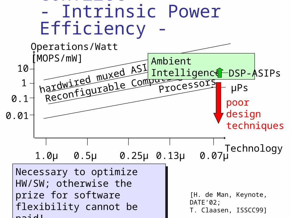
The energy/flexibility conflict- Intrinsic Power Efficiency -
Technology
[H. de Man, Keynote, DATE‘02;T. Claasen, ISSCC99]
Operations/Watt[MOPS/mW]
Processors
Reconfigurable Computinghardwired muxed ASIC
1
0.1
0.01
0.13µ
Necessary to optimize HW/SW; otherwise the prize for software flexibility cannot be paid!
Necessary to optimize HW/SW; otherwise the prize for software flexibility cannot be paid!
Ambient Intelligence
0.07µ
DSP-ASIPs
µPs
10
0.25µ0.5µ1.0µ
poor design techniques

Architectural Choices
P
Prog Mem
MACUnit
AddrGenP
Prog Mem
P
Prog Mem
Satellite
ProcessorDedicated
Logic
Satellite
Processor
Satellite
Processor
GeneralPurpose
P
Software
DirectMapped
Hardware
HardwareReconfigurable
Processor
ProgrammableDSP
Fle
xib
ility
Fle
xib
ility
1/Efficiency (power, speed)1/Efficiency (power, speed)

The Processor Design Space
Cost
Per
form
ance
Microprocessors
Performance iseverything& Software rules
Embeddedprocessors
Microcontrollers
Cost is everything
Application specific architecturesfor performance

Area of processor cores = Cost
Nintendo processor Cellular phones

Another figure of meritComputation per unit area
Nintendo processor Cellular phones???

Embedded vs. general-purpose processors
Embedded processors may be optimized for a category of applications. Customization may be narrow or broad.
We may judge embedded processors using different metrics: Code size. Memory system performance. Preditability.

Microcontrollers
CPUROM RAM
I/O
A single chip
Subsystems:Timers, Counters, AnalogInterfaces, I/O interfaces
Memory

Microcontroller Architectures
CPUProgram + Data
Address Bus
Data Bus
Memory
Von NeumannArchitecture
CPUProgram
Address Bus
Data Bus
HarvardArchitecture
Memory
Data
Address Bus
Fetch Bus
0
0
0
2n

MCS-51 “Family” of Microcontollers
8051 introduced by Intel in late 1970s Now produced by many companies in
many variations The most pupular microcontroller – about
40% of market share 8-bit microcontroller

“Original” 8051 Microcontroller
Oscillator and timing
4096 Bytes Program Memory
128 Bytes Data
Memory
Two 16 Bit Timer/Event
Counters
8051 CPU
64 K Byte Bus Expansion
Control
Programmable I/O
Programmable Serial Port Full Duplex UART
Synchronous Shifter
Internal data bus
External interrupts
subsystem interrupts
Control Parallel portsAddress Data BusI/O pins
Serial InputSerial Output

Microcontrollers- MHS 80C51 as an example -
• 8-bit CPU optimised for control applications• Extensive Boolean processing capabilities• 64 k Program Memory address space• 64 k Data Memory address space• 4 k bytes of on chip Program Memory• 128 bytes of on chip data RAM• 32 bi-directional and individually addressable I/O lines• Two 16-bit timers/counters• Full duplex UART• 6 sources/5-vector interrupt structure with 2 priority levels• On chip clock oscillators• Very popular CPU with many different variations
Featu
res for E
mb
edd
ed S
ystems

RISC processors RISC generally means
highly-pipelinable, one instruction per cycle.
Pipelines of embedded RISC processors have grown over time: ARM7 has 3-stage
pipeline. ARM9 has 5-stage
pipeline. ARM11 has eight-stage
pipeline.
ARM11 pipeline [ARM05].

RISC processor families
ARM: ARM7 is relatively simple, no memory management; ARM11 has memory management, other features.
MIPS: MIPS32 4K has 5-stage pipeline; 4KE family has DSP extension; 4KS is designed for security.
PowerPC: 400 series includes several embedded processors; MPD7410 is two-issue machine; 970FX has 16-stage pipeline.

DSP Applications
Audio applications MPEG Audio Portable audio Digital cameras Wireless Cellular
telephones Base station
Networking Cable modems ADSL VDSL

Another Look at DSP Applications
High-end Wireless Base Station - TMS320C6000 Cable modem gateways
Mid-end Cellular phone - TMS320C540 Fax/ voice server
Low end Storage products - TMS320C27 Digital camera - TMS320C5000 Portable phones Wireless headsets Consumer audio Automobiles, toasters, thermostats, ...
Incr
easi
ngC
ost
Increasingvolum
e

DSP vs. General Purpose MPU
The “MIPS/MFLOPS” of DSPs is speed of Multiply-Accumulate (MAC).
DSP are judged by whether they can keep the multipliers busy 100% of the time.
The "SPEC" of DSPs is 4 algorithms: Inifinite Impule Response (IIR) filters Finite Impule Response (FIR) filters FFT, and convolvers
In DSPs, algorithms are king! Binary compatability not an issue
Software is not (yet) king in DSPs. People still write in assembly language for a product to
minimize the die area for ROM in the DSP chip.

Architectural Features of DSPs
Data path configured for DSP Fixed-point arithmetic MAC- Multiply-accumulate
Multiple memory banks and buses - Harvard Architecture Multiple data memories
Specialized addressing modes Bit-reversed addressing Circular buffers
Specialized instruction set and execution control Zero-overhead loops Support for MAC
Specialized peripherals for DSP THE ULTIMATE IN BENCHMARK DRIVEN ARCHITECTURE
DESIGN!!!

Application: y[j] = i=0
x[j-i]*a[i]
i: 0i n-1: yi[j] = yi-1[j] + x[j-i]*a[i]
Domain-oriented architectures
Architecture: Example: Data path ADSP210x
n-1
- Parallelism - Dedicated registers
MR
MFMX MY
*+,-
AR
AFAX AY
+,-,..
DP
yi-1[j]
x[j-i]
x[j-i]*a[i]
a[i]
Address generation unit (AGU)
Address- registersA0, A1, A2 ..
i+1, j-i+1
ax
MR:=0; A1:=1; A2:=n-2; MX:=x[n-1]; MY:=a[0];for ( j:=1 to n) {MR:=MR+MX*MY; MY:=a[A1]; MX:=x[A2]; A1++; A2--}

DSP - Features (1)
• Multiply/accumulate (MAC) and zero-overhead loop (ZOL) instructions (as shown)
• Heterogeneous registers (as shown)• Separate address generation units (AGUs)
(as in ADSP 210x)

DSP - Features (2)
• Modulo addressing: Am++ Am:=(Am+1) mod n(implements ring or circular buffer in memory)
..x[n-2]x[n-1]x[0]x[1]..
Memory, t=t1
..x[n-3]x[n-2]x[n-1]x[n]x[1]
Memory, t2=t1+1
sliding window
t2xt1
t

Multiple memory banks or memories
MR
MFMX MY
*+,-
AR
AFAX AY
+,-,..
DP
Address generation unit (AGU)
Address- registersA0, A1, A2 ..
Simplifies parallel fetches

Very long instruction word (VLIW) processorsKey idea: detection of possible parallelism to be done by compiler, not by hardware at run-time (inefficient).
VLIW: parallel operations (instructions) encoded in one long word (instruction packet), each instruction controlling one functional unit. E.g.:

The Texas InstrumentsTMS 320C6xx as an example
31 0
0
Instr. A
31 0
0
Instr. D
31 0
1
Instr. F
31 0
0
Instr. G
31 0
1
Instr. E
31 0
1
Instr. C
31 0
1
Instr. B
Cycle Instruction
1 A2 B C D3 E F G
Instructions B, C and D use disjoint functional units, cross paths and other data path resources. The same is also true for E, F and G.
Bit in each instruction encodes end of parallel executionBit in each instruction encodes end of parallel execution
Parallel execution cannot span several packets.Parallel execution cannot span several packets.

Partitioned register files
register file A register file B
L1 S1 M1 D1 D2 M2 S2 L2
Data bus
Address bus
Data path A Data path B
• Many memory ports are required to supply enough operands per cycle.
• Memories with many ports are expensive. Registers are partitioned into (typically 2) sets, e.g. for TI
C60x:

Instruction types are mapped tofunctional unit types
There are 4 functional unit (FU) types: M: Memory Unit I: Integer Unit F: Floating-Point Unit B: Branch Unit
Instruction types corresponding FU type,except type A (mapping to either I or M-functional units).

Large # of delay slots,a problem of VLIW processors
The execution of many instructions has been started before it is realized that a branch was required.Nullifying those instructions would waste compute power Executing those instructions is declared a feature, not a bug. How to fill all „delay slots“ with useful instructions? Avoid branches wherever possible.
add sub and or
sub mult xor div
ld st mv beq

Predicated execution:Implementing IF-statements „branch-free“
Conditional Instruction „[c] I“ consists of:• condition c• instruction I
c = true => I executedc = false => NOP

Predicated execution:Implementing IF-statements „branch-free“: TI C6x
if (c){ a = x + y; b = x + z;}else{ a = x - y; b = x - z;}
Conditional branch
[c] B L1 NOP 5 B L2 NOP 4 SUB x,y,a || SUB x,z,bL1: ADD x,y,a || ADD x,z,bL2:
Predicated execution
[c] ADD x,y,a|| [c] ADD x,z,b|| [!c] SUB x,y,a|| [!c] SUB x,z,b
max. 12 cycles 1 cycle

Roadmap continues: 906545 nm “Traditional” Bus-based SoCs fit in one tile !!
Architecture Evolution
Communication demand is staggering, but unevenly distributed, because of architectural heterogeneity
I/0
I/0
PE
PE PE PE
SRAM SRAM
DRAM
I/O
I/OPERIPHERALS
3D stacked m
ain mem
ory
PE
LocalMemory
hierarchy
CPU
i/o

Multicores Are Here!
1985 199019801970 1975 1995 2000
4004
8008
80868080 286 386 486 Pentium P2 P3P4Itanium
Itanium 2
2005 20??
# of
cor
es
1
2
4
8
16
32
64
128
256
512
Athlon
Raw
Power4Opteron
Power6
Niagara
YonahPExtreme
Tanglewood
Cell
IntelTflops
Xbox360
CaviumOcteon
RazaXLR
PA-8800
CiscoCSR-1
PicochipPC102
Boardcom 1480 Opteron 4P
Xeon MP
AmbricAM2045
[Amarasinghe06]

MPSoC – 2005 ITRS roadmap
2005 2006 2007 2008 2009 2010 2011 2012 2013 2014 2015 2016 2017 2018 2019 2020
0
200
400
600
800
1000
60
50
40
30
20
10
0
1200
Nu
mb
er
of
Pro
ce
ss
ing
En
gin
es
Lo
gic
, M
em
ory
Siz
e (
No
rma
lize
d t
o 2
00
5)
Number of Processing Engines(Right Axis)
Total Logic Size(Normalized to 2005, Left Axis)
Total Memory Size(Normalized to 2005, Left Axis)
16 23 32 4663 79
101133 161
212
268
348
424
526
669
878
[Martin06]

Power is the Challenge!
0
200
400
600
800
1000
1200
1400
90nm 65nm 45nm 32nm 22nm 16nm
Po
wer
(W
), P
ow
er D
ensi
ty (
W/c
m2)
SiO2 Lkg
SD Lkg
Active
10 mm Die
Technology, Circuits, and Architecture to constrain the power
Technology, Circuits, and Architecture to constrain the power

Near Term Solutions Move away from Frequency alone to
deliver performance More on-die memory Multi-everywhere
Multi-threading Chip level multi-processing
Throughput oriented designs Performance by higher level of
integration

Architecture Techniques
0%
25%
50%
75%
100%
1u 0.5u 0.25u 0.13u 65nm
Cac
he
% o
f T
ota
l A
rea
486Pentium®
Pentium® III
Pentium® 4
Pentium® M
Increase on-die Memory
STST Wait for MemWait for Mem
MT1MT1 Wait for MemWait for Mem
MT2MT2 WaitWait
MT3MT3
Single ThreadSingle Thread
Multi-ThreadingMulti-Threading
Full HW UtilizationFull HW Utilization
Multi-threading
Improved performance, no impact on thermals & power delivery
Improved performance, no impact on thermals & power delivery
C1C1 C2C2
C3C3 C4C4
Cache
Chip Multi-processing
LargeCore
LargeCore
1
1.5
2
2.5
3
3.5
1 2 3 4Die Area, Power
Rel
ativ
e P
erfo
rman
ce
Multi Core
Single Core

Multi-Core
C1C1 C2C2
C3C3 C4C4
Cache
Large CoreLarge Core
Cache
1
2
3
4
1
2 SmallCoreSmallCore
1 1
1
2
3
4
1
2
3
4
Power
PerformancePower = 1/4
Performance = 1/2
Multi-Core:Power efficient
Better power and thermal management
Multi-Core:Power efficient
Better power and thermal management

Embedded vs. General Purpose
Embedded Applications Asymmetric Multi-Processing
Differentiated Processors Specific tasks known early
Mapped to dedicated processors Configurable and extensible
processors: performance, power efficiency
Communication Coherent memory Shared local memories HW FIFOS, other direct connections
Dataflow programming models Classical example – Smart mobile –
RISC + DSP + Media processors
Server Applications Symmetric Multi-Processing
Homogeneous cores General tasks known late
Tasks run on any core High-performance, high-speed
microprocessors Communication
large coherent memory space on multi-core die or bus
SMT programming models (Simultaneous Multi-Threading)
Examples: large server chips (eg Sun Niagara 8x4 threads), scientific multi-processors

MPSoC architectures

Example system platforms
Generic Automotive Wireless Multimedia

PC-based platform
Basic hardware components: CPU; memory; timers; DMA; minimal I/O devices.
Basic software: BIOS.

PC-style hardware architecture
CPU
system bus
memory
DMAcontroller
timers
businterface
brid
ge
high-speed bus
low-speed bus
I/O
I/O

Strong ARM
StrongARM system includes: CPU chip (3.686 MHz clock) system control module (32.768 kHz
clock). Real-time clock; operating system timer general-purpose I/O; interrupt controller; power manager controller; reset controller.

Pros and cons
Plentiful hardware options. Simple programming semantics. Good software development
environments. Performance-limited.

TI Open Wireless Multimedia Applications Platform
Dual-processor shared memory system:
GPPOS
DSPmanager
General-purposeprocessor
DSP
DSPOS
DSPtask
& I/Octrl
bridge
Memctrl
external memory
http://www.ti.com/sc/docs/apps/wireless/omap/overview.htm

TI OMAP™ Hardware platform
I-MMU D-MMU
I-Cache
RISC Core
MMU
I-CacheInternal
RAM/ROM
DSP Core+
Appl Coprocessors
DMA
Memory & Traffic Controller
ProgramMemory SDRAM
Peripherals
LCD Controller, Interrupt Handlers, Timers, GPIO, UARTs, ...
ARM9 core 16KB I-
cache 8KB D-cache 2-way set
associative 150 MHz
C55x DSP core
16KB I-cache 8KB RAM set 2-way set
associative 200 MHz
D-Cache

OMAPI Standard (ST/TI)
Goal: standardize the interfaces between application processor and peripheral devices in a mobile product
Provide standard services (APIs) in the OS that can be used by application developers

STMicro Nomadik platformMain Core
Memory System HW Accelerators I/Os

Nomadik SW platform
Compliant with OMAPI standard

Scalable VLIW Media Processor:• 100 to 300+ MHz• 32-bit or 64-bit
Nexperia™
System Buses• 32-128 bit
General-purpose Scalable RISC Processor• 50 to 300+ MHz• 32-bit or 64-bit
Library of DeviceIP Blocks• Image coprocessors• DSPs• UART• 1394• USB…and more
TM-xxxxTM-xxxxTM-xxxxTM-xxxx D$D$
D$D$
I$I$I$I$
TriMedia CPUTriMedia CPU
DEVICE IP BLOCKDEVICE IP BLOCKDEVICE IP BLOCKDEVICE IP BLOCK
DEVICE IP BLOCKDEVICE IP BLOCKDEVICE IP BLOCKDEVICE IP BLOCK
DEVICE IP BLOCKDEVICE IP BLOCKDEVICE IP BLOCKDEVICE IP BLOCK
.. .. ..
DVP SYSTEM SILICON
PI
BU
S
SDRAMSDRAM
MMIMMI
DV
P M
EM
OR
Y
BU
S
DEVICE IP BLOCKDEVICE IP BLOCK
PRxxxxPRxxxxD$
D$
I$I$
MIPS CPU
DEVICE IP BLOCKDEVICE IP BLOCK. . .
DEVICE IP BLOCKDEVICE IP BLOCK
PI
BU
S
TriMedia™MIPS™
Philips Digital Video Nexperia Platform
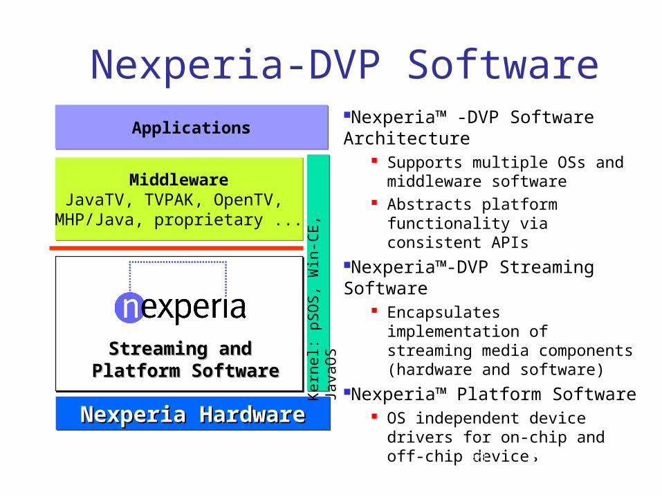
MiddlewareJavaTV, TVPAK, OpenTV, MHP/Java, proprietary ...
MiddlewareJavaTV, TVPAK, OpenTV, MHP/Java, proprietary ...
ApplicationsApplications
Nexperia HardwareNexperia HardwareNexperia HardwareNexperia Hardware
Streaming andStreaming and Platform SoftwarePlatform Software K
erne
l: pS
OS
, Win
-CE
, Ja
vaO
S
Nexperia-DVP SoftwareNexperia™ -DVP Software Architecture
Supports multiple OSs and middleware software
Abstracts platform functionality via consistent APIs
Nexperia™-DVP Streaming Software
Encapsulates implementation of streaming media components (hardware and software)
Nexperia™ Platform Software OS independent device
drivers for on-chip and off-chip devices

Infineon Automotive Platform
TC1166
Applications High Performance drives / servo drives, Industrial control Robotics
Features 32-bit super-scalar TriCoreTM V1.3
CPU, 4 stage pipelineFully integrated DSP capabilitiesSingle precision floating point unit (FPU)80 MHz at full industrial temperature range
32-bit peripheral control processor with single cycle instruction (PCP2)
Memories1.5 MByte embedded progr. flash with ECC32 KByte data flash - EEPROM emulation56 KBSRAM, 8 KB I$, 16 KB Imem
8-channel DMA controller Interrupt system with 2 x 255 hardware
priority arbitration levels serviced by CPU and PCP2 Coprocessor
Triple bus structure: 64-bit local memory buses to internal flash and data memory, 32-bit system peripheral bus, 32-bit remote peripheral bus

HW layerHW layer
SW Platform layer(> 60% of total SW)SW Platform layer(> 60% of total SW)
Application Platform layer(10% of total SW)
Application Platform layer(10% of total SW)
Controllers Library
OSEKRTOS
OSEKCOM
I/O drivers & handlers(> 20 configurable modules)
Application Programming Interface
Boot Loader
Sys. Config.
Transport
KWP 2000
CCP
ApplicationSpecificSoftware
Speedom
eterT
achometer
Water tem
p.
Speedom
eterT
achometer
Odom
eter---------------
ApplicationLibraries
Nec78kNec78k HC12HC12HC08HC08 H8S26H8S26 MB90MB90
SW Platform Reuse> 70%
of total SW
SW Platform Reuse> 70%
of total SW
CustomerLibraries
MOSAIC SW Architecture & Components for Automotive Dashboard and Body Control

Special Purpose processor
Stream processorGraphic processorNetwork processor
Dynamically Reconfigurable Processors
FPGA 、 Reconfigurable systems
Dedicated hardware
ProgrammableHardware
DSP
General purposeCPU
ConfigurableProcessor
Tile Processor
HomogeneousChip-multiprocessor
Specialinstructions
MultipleCores
HeterogeneousMultiprocessor
Multiple Cores
High performance forwide application field
High performance for narrow application fieldArchitecture trends

Task Specific (configurable) Processors
HDL GENERATOR
Silicon
RTL synthesis
Silicon
µcode
Processor modelD
D
Applications
SysC specs
ISA
DP
Courtesy:Target
Compilers T
RWTH AACHEN Lisatek(CoWare);IMEC Target Compiler T, ARM OptimoDEPHILIPS Siliconhive; TENSILICA, PicoChip…
INSTRUCTION SET SIMULATOR
HDLModel Break
Step
RETARGETABLE
COMPILER
Machinecode
MACDAPACSACH Y,1NEGLAR AR3,#X…

Multi-issue instruction
L operations packed in one long instruction
M copies of storage and function
SIMD operation
Parallelism at Three Levels in Extensible Instructions
Parallelism: L x M x NExample: 3 x 4 x 3 = 36 ops/cycle
op
op
N dependent operations
implemented as single
fused operation
const
register and constant inputs
reg
Fused operation
reg reg reg
op
Three forms of instruction-set parallelism:• Very Long Instruction Word (VLIW)
• Single Instruction Multiple Data (SIMD) aka “vectors”
• Fused operations aka “complex operations”

addi addi
l 8 u i
sub
abs
add
l 8 u i
Example:SAD (sum of absolute differences)
short total = 0;char *p1, *p2;for i =1,m for j =1,n total + = abs(*p1++ - *p2++)
Original C Code
SLOT 2SLOT 2
SLOT 1SLOT 1
SLOT 0SLOT 0
Sample Software Pipelined ScheduleVector + Fusion + FL I X Configuration
loop j =1, n / 8 by 2: liu9x8[j]; liu9x8[j]; fusion[j-2] liu9x8[j+1]; liu9x8[j+1]; fusion[j-1]
N O YES
Vectorize?Vectorize?
2
abs9 x 8
cvt9_16
add16 x 8
sub9 x 8
l iu 9 x 8l iu 9 x 8
48
fusion
fusion

Dynamically Reconfigurable Processors
Reconfigurable systems → Previous lesson Flexible but It takes 10’s milliseconds for dynamic
reconfiguration. Dynamically Reconfigurable Processors
Improves area efficiency by changing hardware structure. IPs used in various SoCs. History
Reconfigurable Co-processor Garp(1997), CHIMAERA(2000) Multicontext reconfigurable devices WASMII(1992),Time-multiplexing
FPGA(1997), PipeRench(1998), DRL(1998) Functional-level synthesis
Various commercial products are available since 2000 IPFlex DAPDNA-2, NEC electronics DRP-1, PACT Xpp, Elixent DFabrix
SONY’s VME(Virtual Mobile Engine) is embedded in Network Workman and PSP
Recently, many Japanese vendors start to develop commercial products
Fujitsu Hitachi Lucent Sanyo Toshiba ( Mep+D-Fabrix)

What is Configurable Computing?
Spatially-programmed connection of Spatially-programmed connection of processing elementsprocessing elements
“Hardware” customized to specifics of problem.
Direct map of problem specific dataflow, control.
Circuits “adapted” as problem requirements change.

Spatial vs. Temporal Computing
Spatial Temporal

Processor vs. FPGA Area

Processing Element Specialized for media/stream processing Coarse grain ⇔ Fine grain: LUT of
FPGAs Components
ALU Shifter + Mask unit Multiplexers Registers
Operations and interconnection between components are changeable
No instruction fetch mechanism : A part of large datapath

Reconfigurable HW (DSP fabric)
Target signal processing and arithmetic intensive applications
Reconfigurable array of simple DSP core (CNode)
Low power architecture Hierarchical clock gating Distributed leakage control (fine grain power
gating)
Programmable DMA engine
Reconfigurable at run time, multi task

Mapping Flow
• Alus execute a cyclic micro-sequence
• Data exchanges through hierarchical clustered interconnect
• Configuration step is sequence loading and interconnect programming
Data in Data out
ILP + software pipelining
Procedure(In,Out,inout)
Constant A,b,c,…;
Begin
X=a-in[0];
……..
End;
Behavioral code
Data in Data out
Data in Data out
Data in
Data out
Partitioning/static scheduling
DFG
Coarse grained configuration
MUX
Clusters Level0
Mux level 2
N0_i
N0_o
N2_o N2_i
N1_i N1_o
Level 1

Mapping Flow 3D optimization problem
(place/route/schedule)
Traditional scheduling techniques for VLIW or clustered VLIW don’t apply The solution don’t take into account the spatial
dimension of the problem
Traditional P&R used in FPGA don't apply neither because they don't consider the time dimension

Putting it all together
Constant SoC Die Size Slow evolution of peripherals (area decrease) GP CPU sub-system complexity 2x each node (constant
area), Embedded Memory capacity 2x at each node (constant area) Loosely coupled DSP sub-system complexity increase by
30% at each node (30% area decrease)
2004 2006 2008 2010 2012
Technology Node (nm) 90 65 45 32 22
Loosely coupled Sub-Systems 2 4 6 8 12
General Purpose CPU Single Multiple
Hardware Accelerator Hardwired Reconfigurable

Interconnect
4MB Multi-port Embedded
Memory HostCore 2
L1
L2
Peripherals& analog
What can fit in 45mm² in 45nm
L1
DSP
HW
DMA
L1
DSP
HW
DMA
L1
DSP
HW
DMA
L1
DSP
HW
DMA
L1
DSP
HW
DMA
L1
DSP
HW
DMA
Programmable Multimedia Accelerator
ImagingH/W
192 CNode
(40 GOPS)
HostCore 1
L1
VideoH/W