Hardware Guide - Paoli · TO THE MAXIMUM EXTENT PERMITTED BY APPLICABLE LAW, IN NO EVENT SHALL...
94
HUAWEI MU509 Series HSDPA LGA Module Hardware Guide Issue 09 Date 2014-03-06
Transcript of Hardware Guide - Paoli · TO THE MAXIMUM EXTENT PERMITTED BY APPLICABLE LAW, IN NO EVENT SHALL...
HUAWEI MU509 Series HSDPA LGA Module
Hardware Guide
Issue 09
Date 2014-03-06

Copyright © Huawei Technologies Co., Ltd. 2014. All rights reserved. No part of this manual may be reproduced or transmitted in any form or by any means without prior written consent of Huawei Technologies Co., Ltd. and its affiliates ("Huawei"). The product described in this manual may include copyrighted software of Huawei and possible licensors. Customers shall not in any manner reproduce, distribute, modify, decompile, disassemble, decrypt, extract, reverse engineer, lease, assign, or sublicense the said software, unless such restrictions are prohibited by applicable laws or such actions are approved by respective copyright holders.
Trademarks and Permissions
, , and are trademarks or registered trademarks of Huawei Technologies Co., Ltd. LTE is a trade mark of ETSI. Other trademarks, product, service and company names mentioned may be the property of their respective owners.
Notice Some features of the product and its accessories described herein rely on the software installed, capacities and settings of local network, and therefore may not be activated or may be limited by local network operators or network service providers. Thus, the descriptions herein may not exactly match the product or its accessories which you purchase. Huawei reserves the right to change or modify any information or specifications contained in this manual without prior notice and without any liability.
DISCLAIMER ALL CONTENTS OF THIS MANUAL ARE PROVIDED “AS IS”. EXCEPT AS REQUIRED BY APPLICABLE LAWS, NO WARRANTIES OF ANY KIND, EITHER EXPRESS OR IMPLIED, INCLUDING BUT NOT LIMITED TO, THE IMPLIED WARRANTIES OF MERCHANTABILITY AND FITNESS FOR A PARTICULAR PURPOSE, ARE MADE IN RELATION TO THE ACCURACY, RELIABILITY OR CONTENTS OF THIS MANUAL. TO THE MAXIMUM EXTENT PERMITTED BY APPLICABLE LAW, IN NO EVENT SHALL HUAWEI BE LIABLE FOR ANY SPECIAL, INCIDENTAL, INDIRECT, OR CONSEQUENTIAL DAMAGES, OR LOSS OF PROFITS, BUSINESS, REVENUE, DATA, GOODWILL SAVINGS OR ANTICIPATED SAVINGS REGARDLESS OF WHETHER SUCH LOSSES ARE FORSEEABLE OR NOT. THE MAXIMUM LIABILITY (THIS LIMITATION SHALL NOT APPLY TO LIABILITY FOR PERSONAL INJURY TO THE EXTENT APPLICABLE LAW PROHIBITS SUCH A LIMITATION) OF HUAWEI ARISING FROM THE USE OF THE PRODUCT DESCRIBED IN THIS MANUAL SHALL BE LIMITED TO THE AMOUNT PAID BY CUSTOMERS FOR THE PURCHASE OF THIS PRODUCT.
Import and Export Regulations Customers shall comply with all applicable export or import laws and regulations and be responsible to obtain all necessary governmental permits and licenses in order to export, re-export or import the product mentioned in this manual including the software and technical data therein.
Privacy Policy To better understand how we protect your personal information, please see the privacy policy at http://consumer.huawei.com/privacy-policy.

HUAWEI MU509 Series HSDPA LGA Module Hardware Guide About This Document
Issue 09 (2014-03-06) Huawei Proprietary and Confidential Copyright © Huawei Technologies Co., Ltd. 3
About This Document
Revision History Document Version
Date Chapter Descriptions
01 2010-11-12 Creation
02 2011-04-18 1 Updated Overview
2.2 Updated Table 2-1 Feature
2.4 Updated 2.4 Application Block Diagram
3.1 Updated 3.1 About This Chapter
3.2 Updated Table 3-1 Definitions of pins on the LGA interface
3.3.1 Updated 3.3.1 Overview
3.3.2 Updated 3.3.2 VBAT Interface
3.3.3 Updated 3.3.3 VCOIN Interface
3.4 Updated 3.4 Signal Control Interface
3.5 Updated 3.5 UART Interface
3.6 Added 3.6 USB Interface
3.7 Updated 3.7 SIM Card Interface
3.8 Updated 3.8 Audio Interface
3.9 Added 3.9 General Purpose I/O Interface
3.10 Added 3.10 JTAG Interface
3.11 Added 3.11 RF Antenna Interface
3.12 Added 3.12 NC Pins
4.2 Added 4.2 Antenna Installation Guidelines
4.5.1 Updated 4.5.1 Conducted Receive Sensitivity
4.5.2 Updated 4.5.2 Conducted Transmit Power

HUAWEI MU509 Series HSDPA LGA Module Hardware Guide About This Document
Issue 09 (2014-03-06) Huawei Proprietary and Confidential Copyright © Huawei Technologies Co., Ltd. 4
Document Version
Date Chapter Descriptions
5.5.2 Updated 5.5.2 Power Consumption
6.2 Updated 6.2 Dimensions and interfaces of MU509
6.3 Added 6.3 Customer PCB Pad Design
6.4 Updated 6.4 Label
7 Added 7 Certifications
8 Added 8 Safety Information
9 Added 9 Appendix A Circuit of Typical Interface
10 Updated 10 Appendix B Acronyms and Abbreviations
03 2011-07-08 2.3 Updated the Figure 2-1
3.3.2 Replaced ‘2 mF’ with ‘2.2 mF’
3.4.2 Updated the Figure 3-5 and the Figure 3-6
3.6 Updated the Table 3-10
3.7 Updated the Figure 3-16 and the Figure 3-18
9 Updated the two figures
04 2012-04-23 3.7.2 Updated the value of the resistor which is used to connect the SIM_DATA pin to the VSIM pin.
5.5.2 Updated the Table 5-7
5.5.2 Added the Table 5-9 “DC power consumption for MU509-c(GSM/GPRS/EDGE)”
7.2 Updated the Table 7-1
05 2012-08-27 All Added the content of MU509-g
2.2 Added A-tick in Table 2-1
3.4.1 Updated the description of WAKEUP_IN in Table 3-5
3.4.4 Updated the description of WAKEUP_IN Signal
3.4.5 Updated the description of WAKEUP_OUT Signal

HUAWEI MU509 Series HSDPA LGA Module Hardware Guide About This Document
Issue 09 (2014-03-06) Huawei Proprietary and Confidential Copyright © Huawei Technologies Co., Ltd. 5
Document Version
Date Chapter Descriptions
5.5.2 Update Table 5-6 DC power consumption (Power off mode and Standby mode) and Table 5-7 DC power consumption (Idle mode)
6 Added the process design
7 Updated the CE number
06 2012-12-19 All Added the related content about HUAWEI MU509-1
3.3.2 Updated the peak current to 2.75 V and the storage capacitors to 220 µF
3.3.2 Updated Figure 3-2 Recommended power circuit of MU509 module
3.4.2 Updated Table 3-7 Power off timing
3.4.4 Updated Figure 3-13 WAKEUP_IN sequence
3.5.2 Added the description of level conversion circuit and the wind blow in
07 2013-04-15 2.3 Updated Figure 2-1
3.2 Updated Table 3-1
3.3.1 Updated Table 3-2
3.4.4 Updated Figure 3-13
3.7.2 Updated Figure 3-18
3.10 Updated Table 3-14
4.6.1 Updated Chapter 4.6.1
4.6.3 Updated Chapter 4.6.3
5.2 Updated Table 5-1
9 Updated Chapter 9
08 2013-10-26 2.2 Updated the extended working temperature in Table 2-1
5.3 Updated the extended working temperature in Table 5-2
09 2014-03-06 5.5.2 Updated Power Consumption
5.6 Updated Reliability Features
5.7 Updated EMC and ESD Features

HUAWEI MU509 Series HSDPA LGA Module Hardware Guide About This Document
Issue 09 (2014-03-06) Huawei Proprietary and Confidential Copyright © Huawei Technologies Co., Ltd. 6
Document Version
Date Chapter Descriptions
6.5 Updated the note of packaging
6.6 Updated the note of label
Scope
MU509-b
MU509-c
MU509-g
HUAWEI MU509-1
Summary
This document provides information about the major functions, supported services, system architecture, and technical references of HUAWEI MU509 Series HSDPA LGA Module.
The following table lists the contents of this document.
Chapter Details
1 Introduction Describes the short introduction of the product.
2 Overall Description Describes the Function overview, Circuit Block Diagram and Application Block Diagram of the product.
3 Description of the Application Interfaces
Describes the external application interfaces of the product.
4 RF Specifications Describes the RF specifications of the product.
5 Electrical and Reliability Features Describes the electrical and reliability features of the interfaces in the product.
6 Process Design Describes the process design, the Dimension, Label and Packing System of the product.
7 Certifications Describes the certifications of the product.
8 Safety Information Lists the safety information when using the product.
8 9 Appendix A Circuit of Typical Interface
Lists the circuit of typical interface of the product.

HUAWEI MU509 Series HSDPA LGA Module Hardware Guide About This Document
Issue 09 (2014-03-06) Huawei Proprietary and Confidential Copyright © Huawei Technologies Co., Ltd. 7
Chapter Details
10 Appendix B Acronyms and Abbreviations
Lists the acronyms and abbreviations mentioned in this document.
HUAWEI MU509 Series HSDPA LGA Module Hardware Guide Contents
Issue 09 (2014-03-06) Huawei Proprietary and Confidential Copyright © Huawei Technologies Co., Ltd. 8
Contents
1 Introduction.................................................................................................................................. 11
2 Overall Description .................................................................................................................... 12
2.1 About This Chapter ......................................................................................................................... 12
2.2 Function Overview.......................................................................................................................... 12
2.3 Circuit Block Diagram ..................................................................................................................... 14
2.4 Application Block Diagram ............................................................................................................. 16
3 Description of the Application Interfaces .............................................................................. 17
3.1 About This Chapter ......................................................................................................................... 17
3.2 LGA Interface ................................................................................................................................. 17
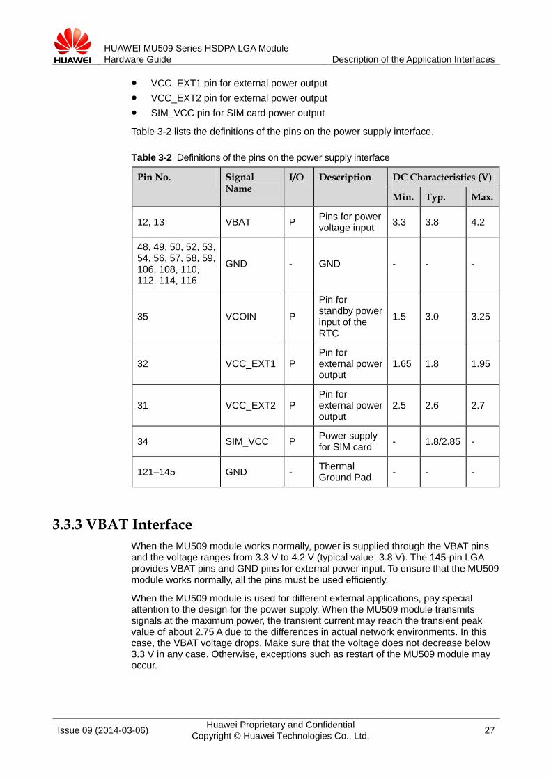
3.3 Power Interface .............................................................................................................................. 26
3.3.1 Overview ................................................................................................................................ 26
3.3.2 VBAT Interface ....................................................................................................................... 27
3.3.3 VCOIN Interface .................................................................................................................... 28
3.3.4 Output Power Supply Interface ............................................................................................. 30
3.4 Signal Control Interface .................................................................................................................. 30
3.4.1 Overview ................................................................................................................................ 30
3.4.2 Input Signal Control Pins ....................................................................................................... 31
3.4.3 Output Signal Control Pin ...................................................................................................... 34
3.4.4 WAKEUP_IN Signal............................................................................................................... 37
3.4.5 WAKEUP_OUT Signal ........................................................................................................... 38
3.5 UART Interface ............................................................................................................................... 39
3.5.1 Overview ................................................................................................................................ 39
3.5.2 Circuit Recommended for the UART Interface ...................................................................... 40
3.6 USB Interface ................................................................................................................................. 40
3.7 SIM Card Interface ......................................................................................................................... 41
3.7.1 Overview ................................................................................................................................ 41
3.7.2 Circuit Recommended for the SIM Card Interface ................................................................ 42
3.8 Audio Interface ............................................................................................................................... 44
3.8.1 Analogue Audio ...................................................................................................................... 44
3.8.2 Digital Audio ........................................................................................................................... 45
3.8.3 Primary Mode ........................................................................................................................ 46
3.9 General Purpose I/O Interface ....................................................................................................... 47
HUAWEI MU509 Series HSDPA LGA Module Hardware Guide Contents
Issue 09 (2014-03-06) Huawei Proprietary and Confidential Copyright © Huawei Technologies Co., Ltd. 9
3.10 JTAG Interface ............................................................................................................................. 47
3.11 RF Antenna Interface.................................................................................................................... 48
3.12 NC Pins ........................................................................................................................................ 48
4 RF Specifications ......................................................................................................................... 49
4.1 About This Chapter ......................................................................................................................... 49
4.2 Antenna Installation Guidelines ...................................................................................................... 49
4.3 Operating Frequencies ................................................................................................................... 49
4.4 Conducted RF Measurement ......................................................................................................... 50
4.4.1 Test Environment ................................................................................................................... 50
4.4.2 Test Standards ....................................................................................................................... 50
4.5 Conducted Rx Sensitivity and Tx Power ........................................................................................ 50
4.5.1 Conducted Receive Sensitivity .............................................................................................. 50
4.5.2 Conducted Transmit Power ................................................................................................... 51
4.6 Antenna Design Requirements ...................................................................................................... 52
4.6.1 Antenna Design Indicators..................................................................................................... 52
4.6.2 Interference ........................................................................................................................... 53
4.6.3 GSM/WCDMA Antenna Requirements .................................................................................. 54
4.6.4 Radio Test Environment ........................................................................................................ 54
5 Electrical and Reliability Features ........................................................................................... 56
5.1 About This Chapter ......................................................................................................................... 56
5.2 Extreme Operating Conditions ....................................................................................................... 56
5.3 Operating and Storage Temperatures and Humidity ...................................................................... 57
5.4 Electrical Features of Application Interfaces .................................................................................. 57
5.5 Power Supply Features .................................................................................................................. 58
5.5.1 Input Power Supply ............................................................................................................... 58
5.5.2 Power Consumption .............................................................................................................. 59
5.6 Reliability Features ......................................................................................................................... 69
5.7 EMC and ESD Features ................................................................................................................. 71
6 Process Design ............................................................................................................................. 74
6.1 About This Chapter ......................................................................................................................... 74
6.2 Storage Requirement ..................................................................................................................... 74
6.3 Moisture Sensitivity ........................................................................................................................ 74
6.4 Dimensions and interfaces ............................................................................................................. 75
6.5 Packaging ....................................................................................................................................... 76
6.6 Label ............................................................................................................................................... 77
6.7 Customer PCB Design ................................................................................................................... 79
6.7.1 PCB Surface Finish ............................................................................................................... 79
6.7.2 PCB Pad Design .................................................................................................................... 79
6.7.3 Solder Mask ........................................................................................................................... 79
6.7.4 Requirements on PCB Layout ............................................................................................... 80
6.8 Assembly Processes ...................................................................................................................... 80

HUAWEI MU509 Series HSDPA LGA Module Hardware Guide Contents
Issue 09 (2014-03-06) Huawei Proprietary and Confidential Copyright © Huawei Technologies Co., Ltd. 10
6.8.1 General Description of Assembly Processes ........................................................................ 80
6.8.2 Stencil Design ........................................................................................................................ 80
6.8.3 Reflow Profile ........................................................................................................................ 81
6.9 Specification of Rework .................................................................................................................. 82
6.9.1 Process of Rework ................................................................................................................ 82
6.9.2 Preparations of Rework ......................................................................................................... 83
6.9.3 Removing of the Module........................................................................................................ 83
6.9.4 Welding Area Treatment ........................................................................................................ 83
6.9.5 Module Installation ................................................................................................................. 84
6.9.6 Specifications of Rework ....................................................................................................... 84
7 Certifications ................................................................................................................................ 85
7.1 About This Chapter ......................................................................................................................... 85
7.2 Certifications ................................................................................................................................... 85
8 Safety Information ...................................................................................................................... 87
8.1 Interference .................................................................................................................................... 87
8.2 Medical Device ............................................................................................................................... 87
8.3 Area with Inflammables and Explosives ......................................................................................... 87
8.4 Traffic Security ................................................................................................................................ 88
8.5 Airline Security ................................................................................................................................ 88
8.6 Safety of Children ........................................................................................................................... 88
8.7 Environment Protection .................................................................................................................. 88
8.8 WEEE Approval .............................................................................................................................. 88
8.9 RoHS Approval ............................................................................................................................... 88
8.10 Laws and Regulations Observance ............................................................................................. 89
8.11 Care and Maintenance ................................................................................................................. 89
8.12 Emergency Call ............................................................................................................................ 89
8.13 Regulatory Information ................................................................................................................. 89
8.13.1 CE Approval (European Union) ........................................................................................... 89
8.13.2 FCC Statement .................................................................................................................... 90
9 Appendix A Circuit of Typical Interface ................................................................................ 91
10 Appendix B Acronyms and Abbreviations .......................................................................... 92
HUAWEI MU509 Series HSDPA LGA Module Hardware Guide Introduction
Issue 09 (2014-03-06) Huawei Proprietary and Confidential Copyright © Huawei Technologies Co., Ltd. 11
1 Introduction
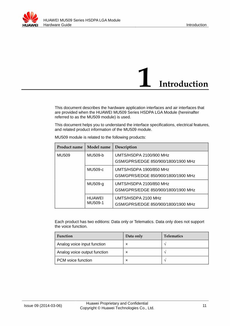
This document describes the hardware application interfaces and air interfaces that are provided when the HUAWEI MU509 Series HSDPA LGA Module (hereinafter referred to as the MU509 module) is used.
This document helps you to understand the interface specifications, electrical features, and related product information of the MU509 module.
MU509 module is related to the following products:
Product name Model name Description
MU509 MU509-b UMTS/HSDPA 2100/900 MHz GSM/GPRS/EDGE 850/900/1800/1900 MHz
MU509-c UMTS/HSDPA 1900/850 MHz GSM/GPRS/EDGE 850/900/1800/1900 MHz
MU509-g UMTS/HSDPA 2100/850 MHz GSM/GPRS/EDGE 850/900/1800/1900 MHz
HUAWEI MU509-1
UMTS/HSDPA 2100 MHz GSM/GPRS/EDGE 850/900/1800/1900 MHz
Each product has two editions: Data only or Telematics. Data only does not support the voice function.
Function Data only Telematics
Analog voice input function × √
Analog voice output function × √
PCM voice function × √
HUAWEI MU509 Series HSDPA LGA Module Hardware Guide Overall Description
Issue 09 (2014-03-06) Huawei Proprietary and Confidential Copyright © Huawei Technologies Co., Ltd. 12
2 Overall Description
2.1 About This Chapter This chapter gives a general description of the MU509 module and provides:
Function Overview Circuit Block Diagram Application Block Diagram
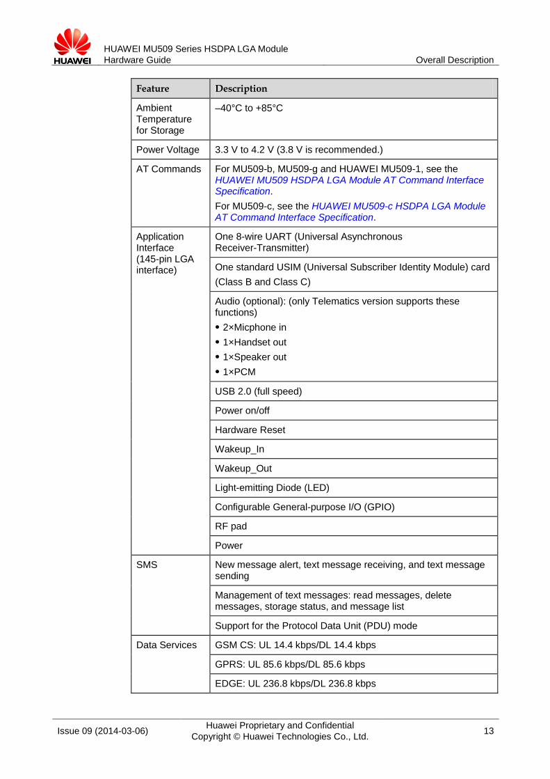
2.2 Function Overview Table 2-1 Feature
Feature Description
Physical Features
Dimensions (L × W × H): 30 mm × 30 mm × 2.6 mm Weight: about 5.5 g
Working Bands MU509-b: UMTS2100/900 MHz GSM850/900/1800/1900 MHz (Data only or Telematics)
MU509-c: UMTS1900/850 MHz GSM850/900/1800/1900 MHz (Data only or Telematics)
MU509-g: UMTS2100/850 MHz GSM850/900/1800/1900 MHz (Data only or Telematics)
HUAWEI MU509-1: UMTS 2100MHz GSM/GPRS/EDGE 850/900/1800/1900 MHz (Data only or Telematics)
For the differences between Data only and Telematics, see "Chapter 1 ".
Operating Temperature
Normal working temperature: –20°C to +70°C
Extended working temperature: –40°C to +85°C
HUAWEI MU509 Series HSDPA LGA Module Hardware Guide Overall Description
Issue 09 (2014-03-06) Huawei Proprietary and Confidential Copyright © Huawei Technologies Co., Ltd. 13
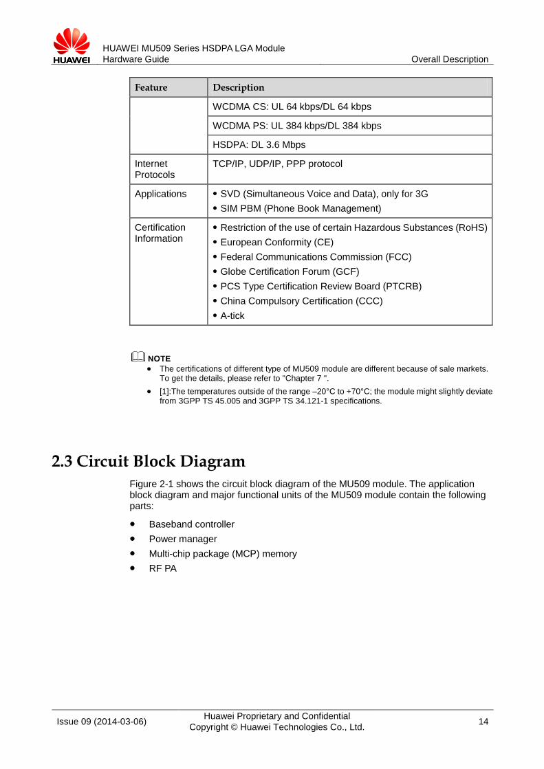
Feature Description
Ambient Temperature for Storage
–40°C to +85°C
Power Voltage 3.3 V to 4.2 V (3.8 V is recommended.)
AT Commands For MU509-b, MU509-g and HUAWEI MU509-1, see the HUAWEI MU509 HSDPA LGA Module AT Command Interface Specification. For MU509-c, see the HUAWEI MU509-c HSDPA LGA Module AT Command Interface Specification.
Application Interface (145-pin LGA interface)
One 8-wire UART (Universal Asynchronous Receiver-Transmitter)
One standard USIM (Universal Subscriber Identity Module) card (Class B and Class C)
Audio (optional): (only Telematics version supports these functions) 2×Micphone in 1×Handset out 1×Speaker out 1×PCM
USB 2.0 (full speed)
Power on/off
Hardware Reset
Wakeup_In
Wakeup_Out
Light-emitting Diode (LED)
Configurable General-purpose I/O (GPIO)
RF pad
Power
SMS New message alert, text message receiving, and text message sending
Management of text messages: read messages, delete messages, storage status, and message list
Support for the Protocol Data Unit (PDU) mode
Data Services GSM CS: UL 14.4 kbps/DL 14.4 kbps
GPRS: UL 85.6 kbps/DL 85.6 kbps
EDGE: UL 236.8 kbps/DL 236.8 kbps
HUAWEI MU509 Series HSDPA LGA Module Hardware Guide Overall Description
Issue 09 (2014-03-06) Huawei Proprietary and Confidential Copyright © Huawei Technologies Co., Ltd. 14
Feature Description
WCDMA CS: UL 64 kbps/DL 64 kbps
WCDMA PS: UL 384 kbps/DL 384 kbps
HSDPA: DL 3.6 Mbps
Internet Protocols
TCP/IP, UDP/IP, PPP protocol
Applications SVD (Simultaneous Voice and Data), only for 3G SIM PBM (Phone Book Management)
Certification Information
Restriction of the use of certain Hazardous Substances (RoHS) European Conformity (CE) Federal Communications Commission (FCC) Globe Certification Forum (GCF) PCS Type Certification Review Board (PTCRB) China Compulsory Certification (CCC) A-tick
The certifications of different type of MU509 module are different because of sale markets.
To get the details, please refer to "Chapter 7 ". [1]:The temperatures outside of the range –20°C to +70°C; the module might slightly deviate
from 3GPP TS 45.005 and 3GPP TS 34.121-1 specifications.
2.3 Circuit Block Diagram Figure 2-1 shows the circuit block diagram of the MU509 module. The application block diagram and major functional units of the MU509 module contain the following parts:
Baseband controller Power manager Multi-chip package (MCP) memory RF PA

HUAWEI MU509 Series HSDPA LGA Module Hardware Guide Overall Description
Issue 09 (2014-03-06) Huawei Proprietary and Confidential Copyright © Huawei Technologies Co., Ltd. 15
Figure 2-1 Circuit block diagram of the MU509 module
Only Telematics version supports the audio function.
Single Chip
BASEBAND
MCP
POWERMANAGER
RF PA
ANTSWITCH
RF
TRAN
SCEIVER
145-pinLG
AC
onnectorinterface
UART
USB
USIM
POWER_ON_OFF
WAKEUP_IN/OUT
LED
RESIN_N
GPIO
AUDIO
JTAG
VBAT
VCC_EXT1
VCC_EXT2
MAIN_ANT
GND

HUAWEI MU509 Series HSDPA LGA Module Hardware Guide Overall Description
Issue 09 (2014-03-06) Huawei Proprietary and Confidential Copyright © Huawei Technologies Co., Ltd. 16
2.4 Application Block Diagram
Figure 2-2 Application block diagram of the MU509 module
UART Interface The module supports 8-wire UART.
USB Interface The USB interface supports USB 2.0 full speed standard.
USIM Interface The USIM interface provides the interface for a USIM card. The USIM card can be inserted into the host side.
Power Supply DC 3.8 V is recommended.
Audio Interface The module supports one speaker output, two microphone input, one earpiece output and one PCM interface (only telematics version supports the audio function).
RF Pad RF antenna interface

HUAWEI MU509 Series HSDPA LGA Module Hardware Guide Description of the Application Interfaces
Issue 09 (2014-03-06) Huawei Proprietary and Confidential Copyright © Huawei Technologies Co., Ltd. 17
3 Description of the Application Interfaces
3.1 About This Chapter This chapter mainly describes the external application interfaces of the MU509 module, including:
LGA Interface Power Interface Signal Control Interface UART Interface USB Interface SIM Card Interface Audio Interface General Purpose I/O Interface JTAG Interface RF Antenna Interface NC Pins
3.2 LGA Interface The MU509 module uses a 145-pin LGA as its external interface. For details about the module and dimensions of the LGA, see " 6.4 Dimensions and interfaces".
If DTE supports other Huawei LGA modules, such as modules with system of CDMA, TD-SCDMA or HSPA, please refer to HUAWEI 30 mm x 30 mm LGA Module Hardware Migration Guide.
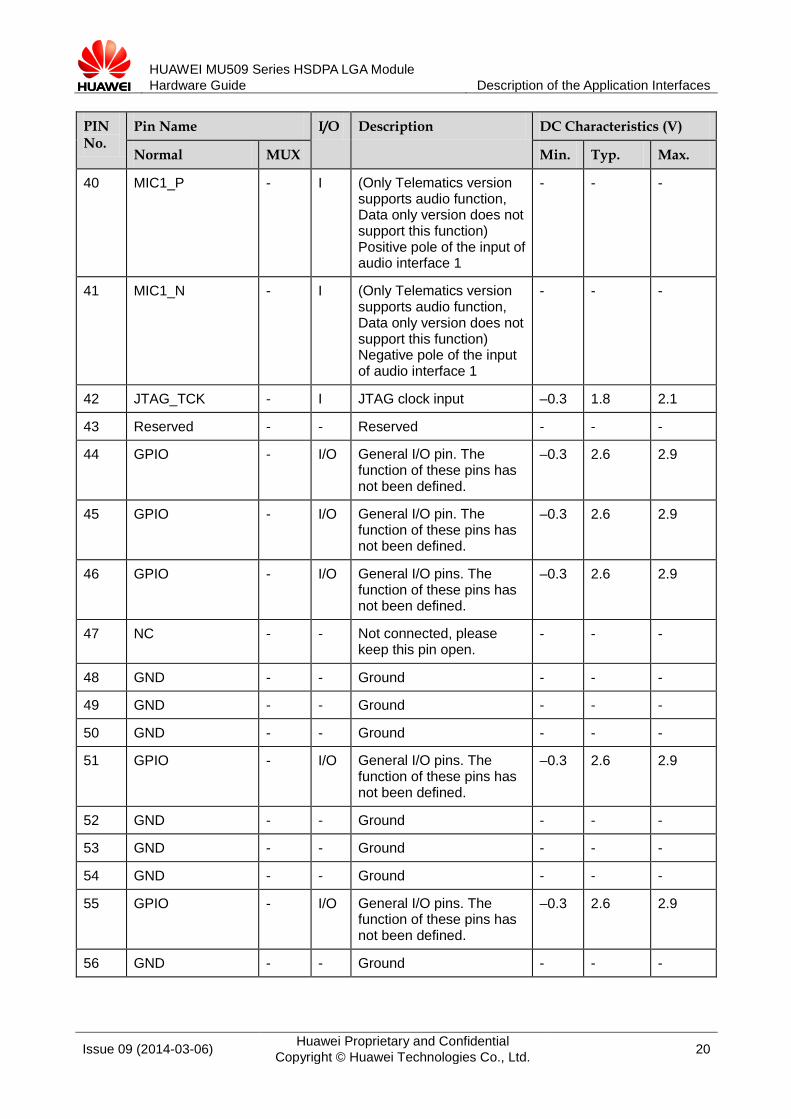
Table 3-1 shows the definitions of pins on the 145-pin signal interface of the MU509 module.

HUAWEI MU509 Series HSDPA LGA Module Hardware Guide Description of the Application Interfaces
Issue 09 (2014-03-06) Huawei Proprietary and Confidential Copyright © Huawei Technologies Co., Ltd. 18
Table 3-1 Definitions of pins on the LGA interface
PIN No.
Pin Name I/O Description DC Characteristics (V)
Normal MUX Min. Typ. Max.
1 NC - - Not connected, please keep this pin open.
- - -
2 NC - - Not connected, please keep this pin open.
- - -
3 NC - - Not connected, please keep this pin open.
- - -
4 NC - - Not connected, please keep this pin open.
- - -
5 PCM_SYNC - O PCM interface sync –0.3 2.6 2.9
6 PCM_DIN - I PCM I/F data in –0.3 2.6 2.9
7 PCM_DOUT - O PCM I/F data out –0.3 2.6 2.9
8 PCM_CLK - O PCM interface clock –0.3 2.6 2.9
9 NC - - Not connected, please keep this pin open.
- - -
10 NC - - Not connected, please keep this pin open.
- - -
11 WAKEUP_IN - I Host to set the module into sleep or wake up the module from sleep.
–0.3 2.6 2.9
12 VBAT - P Power supply input 3.3 3.8 4.2
13 VBAT - P Power supply input 3.3 3.8 4.2
14 PS_HOLD - I Used for JTAG interface assigning a test point for it.
- 1.8 -
15 Reserved - - Reserved - - -
16 NC - - Not connected, please keep this pin open.
- - -
17 NC - - Not connected, please keep open.
- - -
18 NC - - Not connected, please keep this pin open.
- - -
19 NC - - Not connected, please keep this pin open.
- - -
20 NC - - Not connected, please keep this pin open.
- - -
HUAWEI MU509 Series HSDPA LGA Module Hardware Guide Description of the Application Interfaces
Issue 09 (2014-03-06) Huawei Proprietary and Confidential Copyright © Huawei Technologies Co., Ltd. 19
PIN No.
Pin Name I/O Description DC Characteristics (V)
Normal MUX Min. Typ. Max.
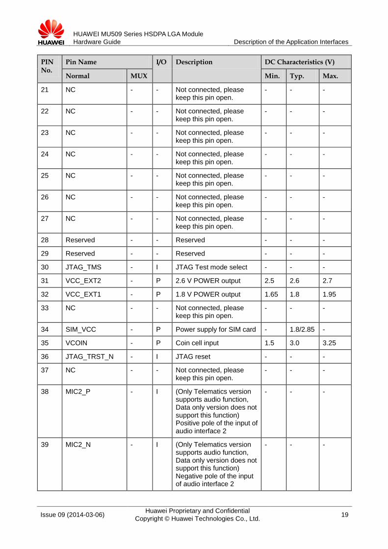
21 NC - - Not connected, please keep this pin open.
- - -
22 NC - - Not connected, please keep this pin open.
- - -
23 NC - - Not connected, please keep this pin open.
- - -
24 NC - - Not connected, please keep this pin open.
- - -
25 NC - - Not connected, please keep this pin open.
- - -
26 NC - - Not connected, please keep this pin open.
- - -
27 NC - - Not connected, please keep this pin open.
- - -
28 Reserved - - Reserved - - -
29 Reserved - - Reserved - - -
30 JTAG_TMS - I JTAG Test mode select - - -
31 VCC_EXT2 - P 2.6 V POWER output 2.5 2.6 2.7
32 VCC_EXT1 - P 1.8 V POWER output 1.65 1.8 1.95
33 NC - - Not connected, please keep this pin open.
- - -
34 SIM_VCC - P Power supply for SIM card - 1.8/2.85 -
35 VCOIN - P Coin cell input 1.5 3.0 3.25
36 JTAG_TRST_N - I JTAG reset - - -
37 NC - - Not connected, please keep this pin open.
- - -
38 MIC2_P - I (Only Telematics version supports audio function, Data only version does not support this function) Positive pole of the input of audio interface 2
- - -
39 MIC2_N - I (Only Telematics version supports audio function, Data only version does not support this function) Negative pole of the input of audio interface 2
- - -
HUAWEI MU509 Series HSDPA LGA Module Hardware Guide Description of the Application Interfaces
Issue 09 (2014-03-06) Huawei Proprietary and Confidential Copyright © Huawei Technologies Co., Ltd. 20
PIN No.
Pin Name I/O Description DC Characteristics (V)
Normal MUX Min. Typ. Max.
40 MIC1_P - I (Only Telematics version supports audio function, Data only version does not support this function) Positive pole of the input of audio interface 1
- - -
41 MIC1_N - I (Only Telematics version supports audio function, Data only version does not support this function) Negative pole of the input of audio interface 1
- - -
42 JTAG_TCK - I JTAG clock input –0.3 1.8 2.1
43 Reserved - - Reserved - - -
44 GPIO - I/O General I/O pin. The function of these pins has not been defined.
–0.3 2.6 2.9
45 GPIO - I/O General I/O pin. The function of these pins has not been defined.
–0.3 2.6 2.9
46 GPIO - I/O General I/O pins. The function of these pins has not been defined.
–0.3 2.6 2.9
47 NC - - Not connected, please keep this pin open.
- - -
48 GND - - Ground - - -
49 GND - - Ground - - -
50 GND - - Ground - - -
51 GPIO - I/O General I/O pins. The function of these pins has not been defined.
–0.3 2.6 2.9
52 GND - - Ground - - -
53 GND - - Ground - - -
54 GND - - Ground - - -
55 GPIO - I/O General I/O pins. The function of these pins has not been defined.
–0.3 2.6 2.9
56 GND - - Ground - - -

HUAWEI MU509 Series HSDPA LGA Module Hardware Guide Description of the Application Interfaces
Issue 09 (2014-03-06) Huawei Proprietary and Confidential Copyright © Huawei Technologies Co., Ltd. 21
PIN No.
Pin Name I/O Description DC Characteristics (V)
Normal MUX Min. Typ. Max.
57 GND - - Ground - - -
58 GND - - Ground - - -
59 GND - - Ground - - -
60 NC - - Not connected, please keep this pin open.
- - -
61 NC - - Not connected, please keep this pin open.
- - -
62 NC - - Not connected, please keep this pin open.
- - -
63 NC - - Not connected, please keep this pin open.
- - -
64 NC - - Not connected, please keep this pin open.
- - -
65 NC - - Not connected, please keep this pin open.
- - -
66 NC - - Not connected, please keep this pin open.
- - -
67 NC - - Not connected, please keep this pin open.
- - -
68 NC - - Not connected, please keep this pin open.
- - -
69 NC - - Not connected, please keep this pin open.
- - -
70 NC - - Not connected, please keep this pin open.
- - -
71 WAKEUP_OUT - O Module to wake up the host
–0.3 2.6 2.9
72 JTAG_TDO - O JTAG test data output –0.3 1.8 2.1
73 UART_DSR - O UART Data Set Ready –0.3 2.6 2.9
74 UART_RTS - O UART Ready for receive –0.3 2.6 2.9
75 UART_DCD - O UART Data Carrier Detect –0.3 2.6 2.9
76 UART_TX - O UART transmit output –0.3 2.6 2.9
77 UART_RING - O UART Ring Indicator –0.3 2.6 2.9
78 UART_RX - I UART receive data input –0.3 2.6 2.9
79 UART_DTR - I Data Terminal Ready –0.3 2.6 2.9
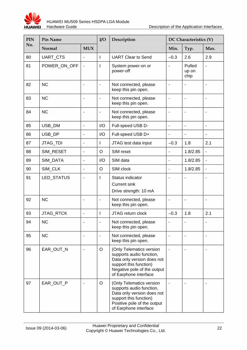
HUAWEI MU509 Series HSDPA LGA Module Hardware Guide Description of the Application Interfaces
Issue 09 (2014-03-06) Huawei Proprietary and Confidential Copyright © Huawei Technologies Co., Ltd. 22
PIN No.
Pin Name I/O Description DC Characteristics (V)
Normal MUX Min. Typ. Max.
80 UART_CTS - I UART Clear to Send –0.3 2.6 2.9
81 POWER_ON_OFF - I System power-on or power-off
- Pulled up on chip
-
82 NC - - Not connected, please keep this pin open.
- - -
83 NC - - Not connected, please keep this pin open.
- - -
84 NC - - Not connected, please keep this pin open.
- - -
85 USB_DM - I/O Full-speed USB D- - - -
86 USB_DP - I/O Full-speed USB D+ - - -
87 JTAG_TDI - I JTAG test data input –0.3 1.8 2.1
88 SIM_RESET - O SIM reset - 1.8/2.85 -
89 SIM_DATA - I/O SIM data - 1.8/2.85 -
90 SIM_CLK - O SIM clock - 1.8/2.85 -
91 LED_STATUS - I Status indicator Current sink Drive strength: 10 mA
- - -
92 NC - - Not connected, please keep this pin open.
- - -
93 JTAG_RTCK - I JTAG return clock –0.3 1.8 2.1
94 NC - - Not connected, please keep this pin open.
- - -
95 NC - - Not connected, please keep this pin open.
- - -
96 EAR_OUT_N - O (Only Telematics version supports audio function, Data only version does not support this function) Negative pole of the output of Earphone interface
- - -
97 EAR_OUT_P - O (Only Telematics version supports audio function, Data only version does not support this function) Positive pole of the output of Earphone interface
- - -
HUAWEI MU509 Series HSDPA LGA Module Hardware Guide Description of the Application Interfaces
Issue 09 (2014-03-06) Huawei Proprietary and Confidential Copyright © Huawei Technologies Co., Ltd. 23
PIN No.
Pin Name I/O Description DC Characteristics (V)
Normal MUX Min. Typ. Max.
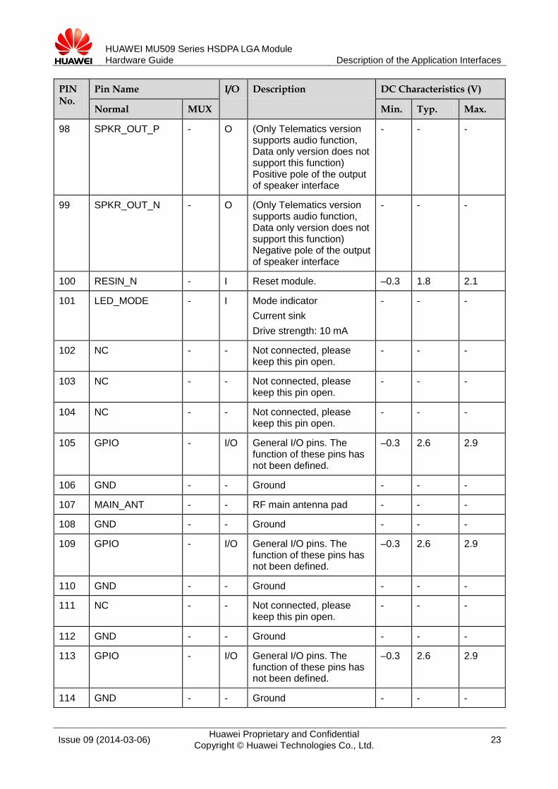
98 SPKR_OUT_P - O (Only Telematics version supports audio function, Data only version does not support this function) Positive pole of the output of speaker interface
- - -
99 SPKR_OUT_N - O (Only Telematics version supports audio function, Data only version does not support this function) Negative pole of the output of speaker interface
- - -
100 RESIN_N - I Reset module. –0.3 1.8 2.1
101 LED_MODE - I Mode indicator Current sink Drive strength: 10 mA
- - -
102 NC - - Not connected, please keep this pin open.
- - -
103 NC - - Not connected, please keep this pin open.
- - -
104 NC - - Not connected, please keep this pin open.
- - -
105 GPIO - I/O General I/O pins. The function of these pins has not been defined.
–0.3 2.6 2.9
106 GND - - Ground - - -
107 MAIN_ANT - - RF main antenna pad - - -
108 GND - - Ground - - -
109 GPIO - I/O General I/O pins. The function of these pins has not been defined.
–0.3 2.6 2.9
110 GND - - Ground - - -
111 NC - - Not connected, please keep this pin open.
- - -
112 GND - - Ground - - -
113 GPIO - I/O General I/O pins. The function of these pins has not been defined.
–0.3 2.6 2.9
114 GND - - Ground - - -
HUAWEI MU509 Series HSDPA LGA Module Hardware Guide Description of the Application Interfaces
Issue 09 (2014-03-06) Huawei Proprietary and Confidential Copyright © Huawei Technologies Co., Ltd. 24
PIN No.
Pin Name I/O Description DC Characteristics (V)
Normal MUX Min. Typ. Max.
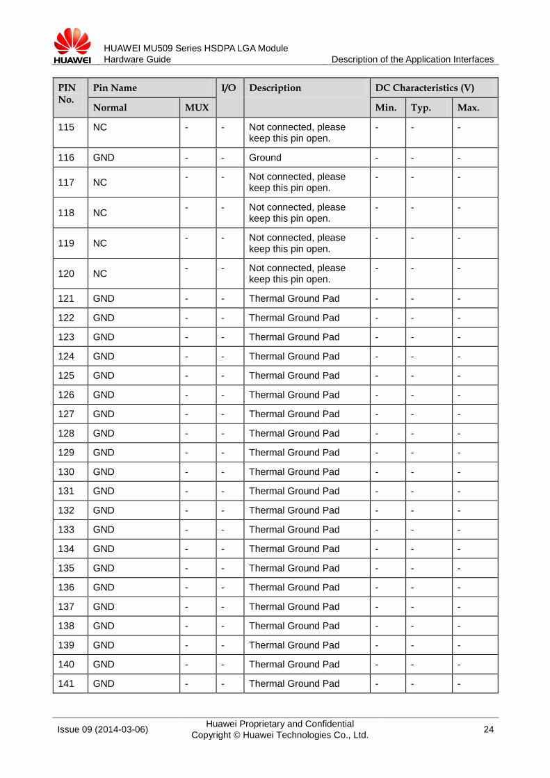
115 NC - - Not connected, please keep this pin open.
- - -
116 GND - - Ground - - -
117 NC - - Not connected, please keep this pin open.
- - -
118 NC - - Not connected, please keep this pin open.
- - -
119 NC - - Not connected, please keep this pin open.
- - -
120 NC - - Not connected, please keep this pin open.
- - -
121 GND - - Thermal Ground Pad - - -
122 GND - - Thermal Ground Pad - - -
123 GND - - Thermal Ground Pad - - -
124 GND - - Thermal Ground Pad - - -
125 GND - - Thermal Ground Pad - - -
126 GND - - Thermal Ground Pad - - -
127 GND - - Thermal Ground Pad - - -
128 GND - - Thermal Ground Pad - - -
129 GND - - Thermal Ground Pad - - -
130 GND - - Thermal Ground Pad - - -
131 GND - - Thermal Ground Pad - - -
132 GND - - Thermal Ground Pad - - -
133 GND - - Thermal Ground Pad - - -
134 GND - - Thermal Ground Pad - - -
135 GND - - Thermal Ground Pad - - -
136 GND - - Thermal Ground Pad - - -
137 GND - - Thermal Ground Pad - - -
138 GND - - Thermal Ground Pad - - -
139 GND - - Thermal Ground Pad - - -
140 GND - - Thermal Ground Pad - - -
141 GND - - Thermal Ground Pad - - -

HUAWEI MU509 Series HSDPA LGA Module Hardware Guide Description of the Application Interfaces
Issue 09 (2014-03-06) Huawei Proprietary and Confidential Copyright © Huawei Technologies Co., Ltd. 25
PIN No.
Pin Name I/O Description DC Characteristics (V)
Normal MUX Min. Typ. Max.
142 GND - - Thermal Ground Pad - - -
143 GND - - Thermal Ground Pad - - -
144 GND - - Thermal Ground Pad - - -
145 GND - - Thermal Ground Pad - - -
P indicates power pins; I indicates pins for digital signal input; O indicates pins for digital
signal output. The NC (Not Connected) pins are internally connected to the module. Therefore, these pins
should not be used, otherwise they may cause problems. Please contact us for more details about this information.
The Reserved pins are internally connected to the module. Therefore, these pins should not be used, otherwise they may cause problems. Please contact with us for more details about this information.

HUAWEI MU509 Series HSDPA LGA Module Hardware Guide Description of the Application Interfaces
Issue 09 (2014-03-06) Huawei Proprietary and Confidential Copyright © Huawei Technologies Co., Ltd. 26
Figure 3-1 shows the sequence of pins on the 145-pin signal interface of the MU509 module.
Figure 3-1 Bottom view of sequence of LGA interface pins
3.3 Power Interface 3.3.2 Overview
The power supply part of the MU509 module contains:
VBAT pins for the power supply VCOIN pin for the standby power supply of the real-time clock (RTC)
30119
118
120
117
31 32 33 34 35 36 37 38 39 40 41 42
43
44
45
46
47
48
49
50
51
52
53
54
55
56
57
14
15
16
17
18
19
20
21
22
23
24
25
26
27
28
29
72
73
74
75
76
77
78
79
80
81
82
83
84
85
86
87
58
88
12345678910111213
59606162636465666768697071
89 90 91 92 93 94 95 96 97 98 99 100 101
102
103
104
105
106
107
108
109
110
111
112
113
114
115
116
121122123124125
136137138139126
135144145140127
134143142141128
133132131130129
Do not use JTAG pads Reserved pads
GND padsPower pads Control pads
UART pads USB pads
RF ant pad
GPIO pads
SIM pads Audio pads
HUAWEI MU509 Series HSDPA LGA Module Hardware Guide Description of the Application Interfaces
Issue 09 (2014-03-06) Huawei Proprietary and Confidential Copyright © Huawei Technologies Co., Ltd. 27
VCC_EXT1 pin for external power output VCC_EXT2 pin for external power output SIM_VCC pin for SIM card power output
Table 3-2 lists the definitions of the pins on the power supply interface.
Table 3-2 Definitions of the pins on the power supply interface
Pin No. Signal Name
I/O Description DC Characteristics (V)
Min. Typ. Max.
12, 13 VBAT P Pins for power voltage input 3.3 3.8 4.2
48, 49, 50, 52, 53, 54, 56, 57, 58, 59, 106, 108, 110, 112, 114, 116
GND - GND - - -
35 VCOIN P
Pin for standby power input of the RTC
1.5 3.0 3.25
32 VCC_EXT1 P Pin for external power output
1.65 1.8 1.95
31 VCC_EXT2 P Pin for external power output
2.5 2.6 2.7
34 SIM_VCC P Power supply for SIM card - 1.8/2.85 -
121–145 GND - Thermal Ground Pad - - -
3.3.3 VBAT Interface When the MU509 module works normally, power is supplied through the VBAT pins and the voltage ranges from 3.3 V to 4.2 V (typical value: 3.8 V). The 145-pin LGA provides VBAT pins and GND pins for external power input. To ensure that the MU509 module works normally, all the pins must be used efficiently.
When the MU509 module is used for different external applications, pay special attention to the design for the power supply. When the MU509 module transmits signals at the maximum power, the transient current may reach the transient peak value of about 2.75 A due to the differences in actual network environments. In this case, the VBAT voltage drops. Make sure that the voltage does not decrease below 3.3 V in any case. Otherwise, exceptions such as restart of the MU509 module may occur.

HUAWEI MU509 Series HSDPA LGA Module Hardware Guide Description of the Application Interfaces
Issue 09 (2014-03-06) Huawei Proprietary and Confidential Copyright © Huawei Technologies Co., Ltd. 28
A low-dropout (LDO) regulator or switch power with current output of more than 3 A is recommended for external power supply. Furthermore, at least five 220 µF storage capacitors are connected in parallel at the power interface of the MU509 module. In addition, to reduce the impact of channel impedance on voltage drop, you are recommended to try to shorten the power supply circuit of the VBAT interface.
It is recommended that add the EMI ferrite bead (NR3015T4R7M manufactured by TAIYO YUDEN or VLS3015T-4R7MR99 manufactured by TDK is recommended) to directly isolate DTE from DCE in the power circuit. Figure 3-2 shows the recommended power circuit of MU509 module.
Figure 3-2 Recommended power circuit of MU509 module
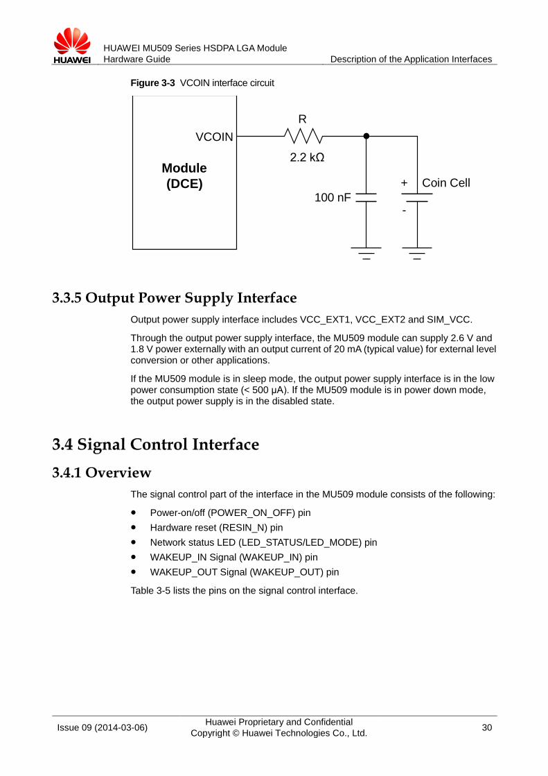
3.3.4 VCOIN Interface VCOIN pin of MU509 module is used as an analog input from the 3 V coin cell for Sudden Momentary Power Loss (SMPL), Real-time Clock (RTC) and External Crystal Oscillator (XTAL) keep-alive power. A capacitor (rather than a coin cell) can be used if only SMPL is supported (not RTC or XTAL). VCOIN pin is also used as an analog output for a coin cell or a capacitor charging.
Sudden momentary power loss If the monitored VBAT drops out-of-range (< 2.55 V nominal), the SMPL feature initiates a power-on sequence without software intervention, and then VBAT returns in-range within a programmable interval of between 0.5 and 2.0 seconds. SMPL achieves immediate and automatic recovery from momentary power loss. A valid voltage on VCOIN is required to run the SMPL timer. If a capacitor is used instead of a coin, it must be connected between VCOIN and the ground. The capacitor must be charged to operate properly as the SMPL power source. The capacitor value depends on the SMPL timer setting.
Module (DCE)
VBATVBAT
100 nF10 μF
+
220 μF
+
220 μF
+
220 μF
+
220 μF
+
220 μF
HUAWEI MU509 Series HSDPA LGA Module Hardware Guide Description of the Application Interfaces
Issue 09 (2014-03-06) Huawei Proprietary and Confidential Copyright © Huawei Technologies Co., Ltd. 29
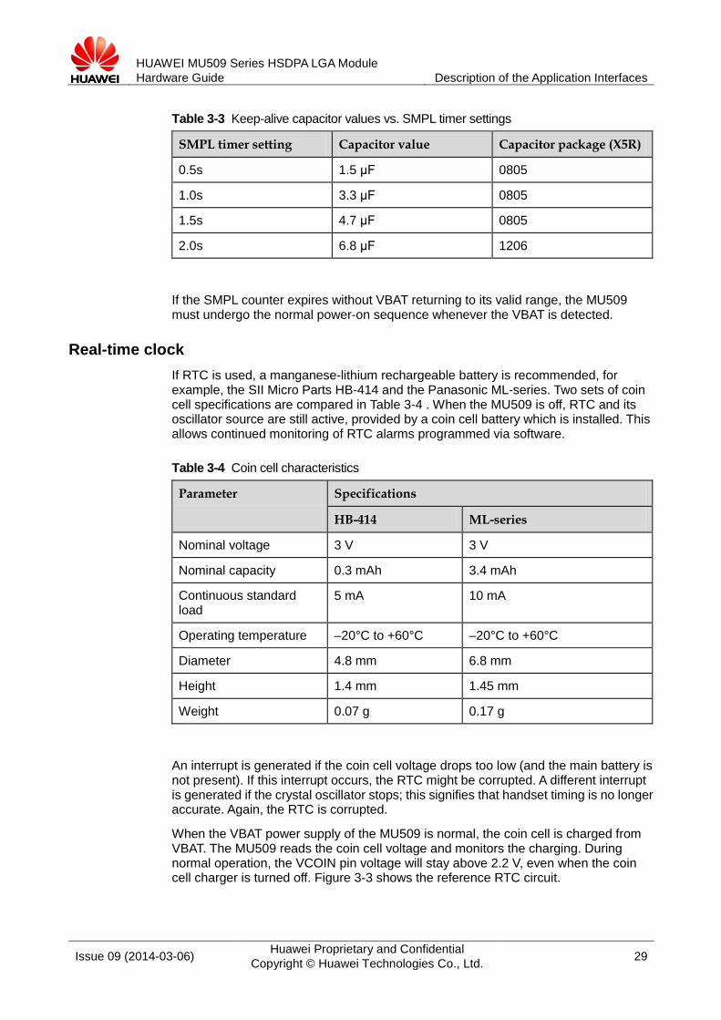
Table 3-3 Keep-alive capacitor values vs. SMPL timer settings
SMPL timer setting Capacitor value Capacitor package (X5R)
0.5s 1.5 μF 0805
1.0s 3.3 μF 0805
1.5s 4.7 μF 0805
2.0s 6.8 μF 1206
If the SMPL counter expires without VBAT returning to its valid range, the MU509 must undergo the normal power-on sequence whenever the VBAT is detected.
Real-time clock If RTC is used, a manganese-lithium rechargeable battery is recommended, for example, the SII Micro Parts HB-414 and the Panasonic ML-series. Two sets of coin cell specifications are compared in Table 3-4 . When the MU509 is off, RTC and its oscillator source are still active, provided by a coin cell battery which is installed. This allows continued monitoring of RTC alarms programmed via software.
Table 3-4 Coin cell characteristics
Parameter Specifications
HB-414 ML-series
Nominal voltage 3 V 3 V
Nominal capacity 0.3 mAh 3.4 mAh
Continuous standard load
5 mA 10 mA
Operating temperature –20°C to +60°C –20°C to +60°C
Diameter 4.8 mm 6.8 mm
Height 1.4 mm 1.45 mm
Weight 0.07 g 0.17 g
An interrupt is generated if the coin cell voltage drops too low (and the main battery is not present). If this interrupt occurs, the RTC might be corrupted. A different interrupt is generated if the crystal oscillator stops; this signifies that handset timing is no longer accurate. Again, the RTC is corrupted.
When the VBAT power supply of the MU509 is normal, the coin cell is charged from VBAT. The MU509 reads the coin cell voltage and monitors the charging. During normal operation, the VCOIN pin voltage will stay above 2.2 V, even when the coin cell charger is turned off. Figure 3-3 shows the reference RTC circuit.
HUAWEI MU509 Series HSDPA LGA Module Hardware Guide Description of the Application Interfaces
Issue 09 (2014-03-06) Huawei Proprietary and Confidential Copyright © Huawei Technologies Co., Ltd. 30
Figure 3-3 VCOIN interface circuit
3.3.5 Output Power Supply Interface Output power supply interface includes VCC_EXT1, VCC_EXT2 and SIM_VCC.
Through the output power supply interface, the MU509 module can supply 2.6 V and 1.8 V power externally with an output current of 20 mA (typical value) for external level conversion or other applications.
If the MU509 module is in sleep mode, the output power supply interface is in the low power consumption state (< 500 μA). If the MU509 module is in power down mode, the output power supply is in the disabled state.
3.4 Signal Control Interface 3.4.1 Overview
The signal control part of the interface in the MU509 module consists of the following:
Power-on/off (POWER_ON_OFF) pin Hardware reset (RESIN_N) pin Network status LED (LED_STATUS/LED_MODE) pin WAKEUP_IN Signal (WAKEUP_IN) pin WAKEUP_OUT Signal (WAKEUP_OUT) pin
Table 3-5 lists the pins on the signal control interface.
Module(DCE)
VCOIN
Coin Cell100 nF
+
-
2.2 kΩ
R
HUAWEI MU509 Series HSDPA LGA Module Hardware Guide Description of the Application Interfaces
Issue 09 (2014-03-06) Huawei Proprietary and Confidential Copyright © Huawei Technologies Co., Ltd. 31
Table 3-5 Pins on the signal control interface
Pin No.
Pin Name I/O Description DC Characteristics (V)
Min. Typ. Max.
81 POWER_ON_OFF I Pin for controlling power-on and power-off
- Pulled up on chip -
100 RESIN_N I Pin for resetting the hardware –0.3 1.8 2.1
91 LED_STATUS I Pin for network status LED - - -
101 LED_MODE I Pin for network mode LED - - -
11 WAKEUP_IN I
Host to set the module into forced sleep or wake up the module from forced sleep
–0.3 2.6 2.9
71 WAKEUP_OUT O Module to wake up the host. –0.3 2.6 2.9
It is recommended to use resistance of 0 Ω in the DTE to isolate signals transmitted from above pins in Table 3-5 .
3.4.2 Input Signal Control Pins The MU509 module implements power-on and power-off and resets the hardware through the input signal control pins.
The power-on, power-off, and reset control parts of the interface of the MU509 module include power-on/power-off interface signal (POWER_ON_OFF) and the hardware reset interface signal (RESIN_N).
The POWER_ON_OFF pin is used to implement power-on and power-off. If the POWER_ON_OFF pin is pulled down for at least 0.5s, the module is powered on; if the POWER_ON_OFF pin is pulled down for at least 0.5s again, the module is powered off.
The RESIN_N pin is used to reset the hardware. When the software stops responding, the RESIN_N pin can be pulled down for at least 10 ms to reset the hardware.
HUAWEI MU509 Series HSDPA LGA Module Hardware Guide Description of the Application Interfaces
Issue 09 (2014-03-06) Huawei Proprietary and Confidential Copyright © Huawei Technologies Co., Ltd. 32
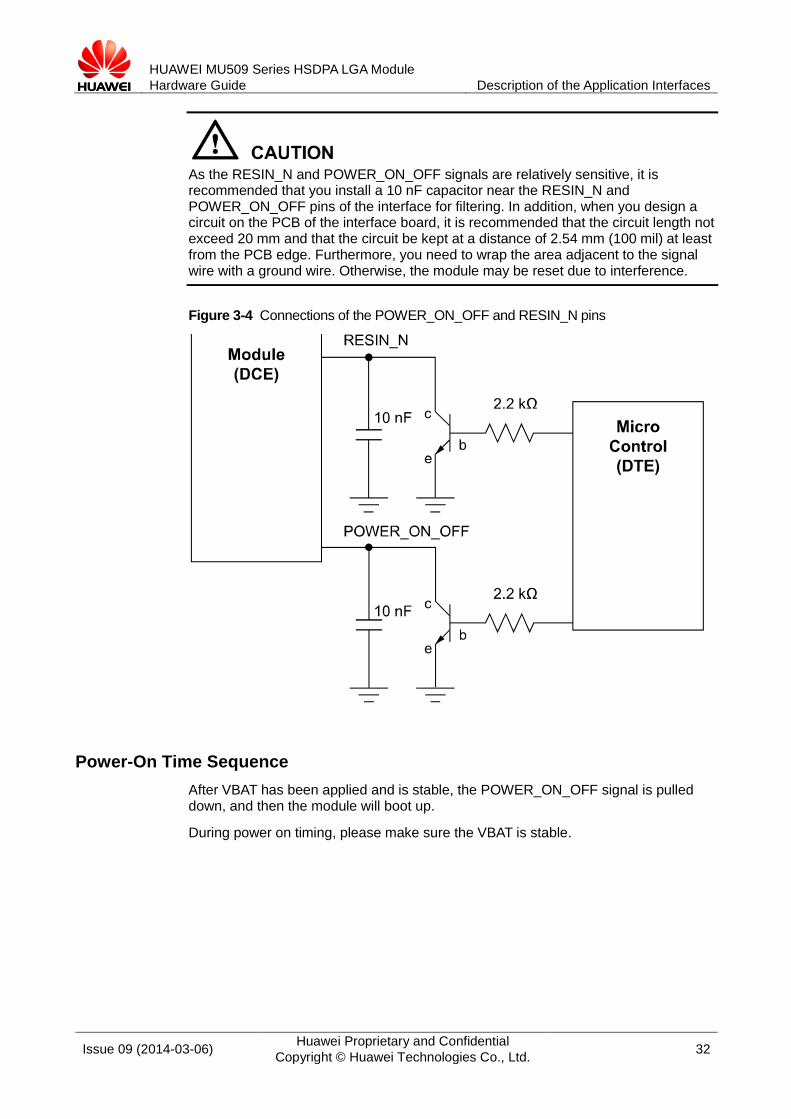
As the RESIN_N and POWER_ON_OFF signals are relatively sensitive, it is recommended that you install a 10 nF capacitor near the RESIN_N and POWER_ON_OFF pins of the interface for filtering. In addition, when you design a circuit on the PCB of the interface board, it is recommended that the circuit length not exceed 20 mm and that the circuit be kept at a distance of 2.54 mm (100 mil) at least from the PCB edge. Furthermore, you need to wrap the area adjacent to the signal wire with a ground wire. Otherwise, the module may be reset due to interference.
Figure 3-4 Connections of the POWER_ON_OFF and RESIN_N pins
Power-On Time Sequence After VBAT has been applied and is stable, the POWER_ON_OFF signal is pulled down, and then the module will boot up.
During power on timing, please make sure the VBAT is stable.

HUAWEI MU509 Series HSDPA LGA Module Hardware Guide Description of the Application Interfaces
Issue 09 (2014-03-06) Huawei Proprietary and Confidential Copyright © Huawei Technologies Co., Ltd. 33
Figure 3-5 Power on timing sequence
Table 3-6 Power on timing
Parameter Comments Time(Nominal values) Units
TPON POWER_ON_OFF turn on time. 0.5 < TPON < 1 s
TPD+ POWER_ON_OFF Valid to USB D+ high
4 s
If the DTE needs to detect the PID/VID of module during the BIOS phase, the detection time should exceed the TPD+ time.
Figure 3-6 Power off timing
Table 3-7 Power off timing
Parameter Comments Time(Nominal values) Units
TPOFF POWER_ON_OFF turn off time. 0.5 < TPOFF < 4 s
TPD+ POWER_ON_OFF Valid to USB D+ high
4.6 s
HUAWEI MU509 Series HSDPA LGA Module Hardware Guide Description of the Application Interfaces
Issue 09 (2014-03-06) Huawei Proprietary and Confidential Copyright © Huawei Technologies Co., Ltd. 34
For detailed information about power supply design and printed circuit board (PCB) design, see the HUAWEI Module Power Supply Design Guide and the HUAWEI LGA Module PCB Routing Design Guide.
RESIN_N The MU509 module supports hardware reset function. If the software of the MU509 module stops responding, you can reset the hardware through the RESIN_N signal as shown in Figure 3-7 .When a low-level pulse is supplied through the RESIN_N pin for more than 50 ms, the hardware will be reset. After the hardware is reset, the software starts powering on the module and reports relevant information according to the actual settings. For example, the AT command automatically reports ^SYSSTART.
Figure 3-7 Reset pulse timing
The low-level pulse through the RESET pin cannot last for more than 2s. Otherwise, the MU509 module will be powered off.
3.4.3 Output Signal Control Pin The MU509 module provides a network status LED pin LED_STATUS and LED_MODE. The pulse signal output through this pin controls the status LED on the user interface board to display the network status. The LEDs are controlled by a current sink. The high voltage is the voltage of VBAT (with the typical value of 3.8 V).
Different blinking modes of the status LED indicate different network status. Table 3-8 describes the status of the LED_STATUS pin and LED_MODE pin.
Table 3-8 The status of the LED_STATUS pin and LED_MODE pin
No. Operating Status LED_STATUS LED_MODE
1 The 3G network is successfully registered.
The indicator blinks once each time. Light off
2 The dial-up connection is set up for accessing 3G data services.
Light on Light off
3 The software is being downloaded or upgraded. Light off The indicator blinks fast.
4 The network is being searched for or no network is detected.
Light off The indicator blinks twice each time.
OPEN
GND
50 ms ~ 100 msRESIN_N

HUAWEI MU509 Series HSDPA LGA Module Hardware Guide Description of the Application Interfaces
Issue 09 (2014-03-06) Huawei Proprietary and Confidential Copyright © Huawei Technologies Co., Ltd. 35
No. Operating Status LED_STATUS LED_MODE
5 The 2G network is successfully registered. Light off The indicator blinks
once each time.
6 The dial-up connection is set up for accessing 2G data services.
Light off Light on
Blinking Once Each Time
Figure 3-8 Status when the indictor blinks once each time
Blinking Fast
Figure 3-9 Status when the indictor blinks fast
light on
100ms
1 cycle: 3s
light off
Light on
100ms
1 cycle: 200ms
Light off

HUAWEI MU509 Series HSDPA LGA Module Hardware Guide Description of the Application Interfaces
Issue 09 (2014-03-06) Huawei Proprietary and Confidential Copyright © Huawei Technologies Co., Ltd. 36
Blinking Twice Each Time
Figure 3-10 Status when the indictor blinks twice each time
External Circuits Figure 3-11 shows the recommended circuits of the LED_MODE and LED_STATUS pins. According to LED feature, you can adjust the LED brightness by adjusting the impedance of resistor R.
Figure 3-11 Driving circuit
For resistance of R placed on user board, choose the value such that it satisfies the following equation:
IF *R+VF = VBAT
VF: Forward voltage
IF: Forward current
Take a LED as an example, Figure 3-12 shows its IF - VF curves. If VBAT is 3.8 V and the desired current through the LED IF is 3 mA, then the voltage of the LED VF is 1.5 V according to IF - VF curves, and the corresponding value for resistance of R is (3.8-1.5)/0.003 = 767 Ω.
The brightness of the LED depends on the current value, and for most of the indicator lights the current from 2 mA to 5 mA is already enough.
Light on
100ms
1 cycle: 3s
Light off
100ms 100ms
R
LED_STATUS
LED_MODE
R
VBAT
VF IF
VF IF
Module(DCE)

HUAWEI MU509 Series HSDPA LGA Module Hardware Guide Description of the Application Interfaces
Issue 09 (2014-03-06) Huawei Proprietary and Confidential Copyright © Huawei Technologies Co., Ltd. 37
Figure 3-12 LED Typical Electro-Optical Characteristics Curves
3.4.4 WAKEUP_IN Signal The DTE controls the sleep and wakeup status of the MU509 module through the WAKEUP_IN signal. The DTE can control the MU509 module to enter forced sleep status in following two cases:
1. Before MU509 module is powered on, if the WAKEUP_IN pin carries a low-level voltage, MU509 module is allowed to enter forced sleep status after MU509 module is powered on.
2. After MU509 module is powered on, if WAKEUP_IN pin's level status changes from high to low (that is, the pin level is in falling edge), MU509 module is allowed to enter forced sleep status.
If the level status of the WAKEUP_IN signal changes from low to high when the MU509 module is in forced sleep status, the MU509 module will exit from forced sleep status.
Figure 3-13 WAKEUP_IN sequence
Low Low
HighRising edge Falling edge
WAKEUP_IN
the MU509 module statusPower onBefore power on
Forced sl eep status Forced sl eep status
Normal status
HUAWEI MU509 Series HSDPA LGA Module
Hardware Guide Description of the Application Interfaces
Issue 09 (2014-03-06) Huawei Proprietary and Confidential
Copyright © Huawei Technologies Co., Ltd. 38
The level status of WAKEUP_IN signal is high by default.
3.4.5 WAKEUP_OUT Signal
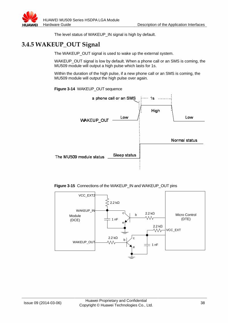
The WAKEUP_OUT signal is used to wake up the external system.
WAKEUP_OUT signal is low by default. When a phone call or an SMS is coming, the MU509 module will output a high pulse which lasts for 1s.
Within the duration of the high pulse, if a new phone call or an SMS is coming, the MU509 module will output the high pulse over again.
Figure 3-14 WAKEUP_OUT sequence
Figure 3-15 Connections of the WAKEUP_IN and WAKEUP_OUT pins
VCC_EXT
VCC_EXT2
WAKEUP_IN
WAKEUP_OUT
b
b
c
c
e
e
2.2 kΩ
2.2 kΩ
2.2 kΩ
2.2 kΩ
1 nF
1 nF
Module
(DCE)
Micro Control
(DTE)

HUAWEI MU509 Series HSDPA LGA Module Hardware Guide Description of the Application Interfaces
Issue 09 (2014-03-06) Huawei Proprietary and Confidential Copyright © Huawei Technologies Co., Ltd. 39
3.5 UART Interface 3.5.1 Overview
The MU509 module provides the UART (8-wire UART) interface for one asynchronous communication channel. As the UART interface supports signal control through standard modem handshake, AT commands are entered and serial communication is performed through the UART interface. The UART has the following features:
Full-duplex 7-bit or 8-bit data 1-bit or 2-bit stop bit Odd parity check, even parity check, or non-check Baud rate clock generated by the system clock Direct memory access (DMA) transmission Baud rate ranging from 600 bit/s to 230400 bit/s (115200 bit/s by default)
Table 3-9 lists the UART interface signals.
Table 3-9 UART interface signals
Pin No.
Pin Name I/O Description DC Characteristics (V)
Min. Typ. Max.
76 UART_TX O Data sending on the wireless module
–0.3 2.6 2.9
78 UART_RX I Data receive end of the module
–0.3 2.6 2.9
77 UART_RING O Ringing indication on the wireless module
–0.3 2.6 2.9
74 UART_RTS O Data sending request on the wireless module
–0.3 2.6 2.9
79 UART_DTR I Data terminal ready on the wireless module
–0.3 2.6 2.9
80 UART_CTS I Clearing to send on the wireless module
–0.3 2.6 2.9
75 UART_DCD O Data carrier detection on the wireless module
–0.3 2.6 2.9
73 UART_DSR O Data ready on the wireless module
–0.3 2.6 2.9

HUAWEI MU509 Series HSDPA LGA Module Hardware Guide Description of the Application Interfaces
Issue 09 (2014-03-06) Huawei Proprietary and Confidential Copyright © Huawei Technologies Co., Ltd. 40
3.5.2 Circuit Recommended for the UART Interface Figure 3-16 shows the connection of the UART interface in the MU509 module (DCE) with the host (DTE).
Figure 3-16 Connection of the UART interface in the MU509 module (DCE) with the host (DTE)
For detailed application of the MU509 UART interface, see the HUAWEI Module UART
Serial Port Design Guide. It is recommended that set the pins related to UART interface as test points on the DTE
board for debugging. The maximum level of UART interface signals is 2.9 V. If these signals are connected to a
host with 3.3 V level, a level conversion circuit is required. Make sure that the level of the UART signals are 0 V before MU509 module is powered on
to avoid the wind blow in which may cause the module cannot work properly. The level of RS-232 Transceivers must match that of the MU509 module.
3.6 USB Interface The MU509 is compliant with USB 2.0 full speed protocol. Figure 3-17 shows the circuit of the USB interface.
Table 3-10 Definition of the USB interface
Pin No. Pin Name I/O Description DC Characteristics (V)
Min. Typ. Max.
86 USB_DP I/O USB data signal D+ - - -
85 USB_DM I/O USB data signal D- - - -
UART_TXUART_RX
UART_CTSUART_RTSUART_DTRUART_DSRUART_DCD
UART_RING
TXDRXDRTSCTSDTRDSRDCDRING
Module(DCE)
Application(DTE)

HUAWEI MU509 Series HSDPA LGA Module Hardware Guide Description of the Application Interfaces
Issue 09 (2014-03-06) Huawei Proprietary and Confidential Copyright © Huawei Technologies Co., Ltd. 41
According to USB protocol, for bus timing or electrical characteristics of MU509 USB signal, please refer to the chapter 7.3.2 of Universal Serial Bus Specification 2.0.
Figure 3-17 Recommended circuit of USB interface
Since the USB interface of MU509 module supports USB 2.0 full speed, the resistance
"RV102 and RV103" in the Figure 3-17 must be Voltage Sensitive Resistor with small capacitance (ALVC18S02003 manufactured by AMOTECH or B72590T7900V60 manufactured by EPCOS is recommended.). In addition, the layout design of this circuit on the DTE board should comply with the USB 2.0 full speed protocol, with differential lining and impedance control to 90 Ω.
It is recommended that set USB_DM and USB_DP pins as test points and then place these test points on the DTE for debugging.
3.7 SIM Card Interface 3.7.1 Overview
The MU509 module provides a SIM card interface complying with the ISO 7816-3 standard and supports automatic detection of a Class B SIM card or a Class C SIM card. Table 3-11 lists the SIM card interface signals.
RV
102
J2
GND
P1 12345
67
89
P2P3P4P5
S1S2
M1M2
USB_D P
USB_DM
RV
103

HUAWEI MU509 Series HSDPA LGA Module Hardware Guide Description of the Application Interfaces
Issue 09 (2014-03-06) Huawei Proprietary and Confidential Copyright © Huawei Technologies Co., Ltd. 42
Table 3-11 SIM card interface signals
Pin No. Pin Name I/O Description DC Characteristics (V)
Min. Typ. Max.
34 SIM_VCC P Power source for the external USIM. - 1.8/2.85 -
89 SIM_DATA I/O
External USIM data signal. - 1.8/2.85 -
90 SIM_CLK O External USIM clock signal. - 1.8/2.85 -
88 SIM_RESET O External USIM reset signal. - 1.8/2.85 -
3.7.2 Circuit Recommended for the SIM Card Interface As the MU509 module is not equipped with a SIM card socket, you need to place a SIM card socket on the user interface board. The SIM card signals are transmitted outwards through the 145-pin LGA interface. Figure 3-18 shows the circuit of the SIM card interface.
Figure 3-18 Circuit of the SIM card interface

HUAWEI MU509 Series HSDPA LGA Module Hardware Guide Description of the Application Interfaces
Issue 09 (2014-03-06) Huawei Proprietary and Confidential Copyright © Huawei Technologies Co., Ltd. 43
Figure 3-19 Pin definition of SIM Socket
pin1: SIM_VCC
pin2: SIM_RESET
pin3: SIM_CLK
pin4: GND
pin5: NULL
pin6: SIM_DATA
HUAWEI MU509 Series HSDPA LGA Module Hardware Guide Description of the Application Interfaces
Issue 09 (2014-03-06) Huawei Proprietary and Confidential Copyright © Huawei Technologies Co., Ltd. 44
To meet the requirements of 3GPP TS 51.010-1 protocols and electromagnetic
compatibility (EMC) authentication, the SIM card socket should be placed near the LGA interface (it is recommended that the PCB circuit connecting the LGA interface and the SIM card socket not exceed 100 mm), because a long circuit may lead to wave distortion, thus affecting signal quality.
It is recommended that you wrap the area adjacent to the SIM_CLK and SIM_DATA signal wires with a ground wire. The GND pin of the SIM card socket and the GND pin of the SIM card must be well connected to the power GND pin supplying power to the MU509 module.
A 0.1 μF or a 0.22 μF capacitor and a 1 μF capacitor are placed between the SIM_VCC and GND pins in a parallel manner. Three 10 pF capacitors are placed between the SIM_DATA and GND pins, the SIM_RST and GND pins, and the SIM_CLK and GND pins in parallel to filter interference from RF signals.
You do not need to pull the SIM_DATA pin up during design as a 20000-Ω resistor is used to connect the SIM_DATA pin to the VSIM pin.
It is recommended to take electrostatic discharge (ESD) protection measures near the USIM card socket. The TVS diode with Vrwm of 5 V and junction capacitance less than 10 pF must be placed as close as possible to the USIM socket, and the Ground pin of the ESD protection component is well connected to the power Ground pin that supplies power to the MU509 module.
3.8 Audio Interface 3.8.1 Analogue Audio
The MU509 provides two audio I/O channels (Data only does not support the voice function).
The two audio I/O channels are completely different and thus have good performance of resisting RF interferences. The routes on the printed circuit board (PCB) should be placed in parallel with each other and should be short. The filter circuit on the two sides should be symmetric. The differential signals should be close to each other. The audio output signals in differential pairs and the audio input signals in differential pairs should be separated effectively through ground. In addition, the audio signals should be located away from the circuits of the power supply, RF, and antenna.
The first audio channel can be used for the handset without requiring any audio amplifier. The output power for the differential ear output is typically 50 mW into a 32 Ω speaker.
The second audio channel can be used for the hands-free without requiring any audio amplifier. The output pins are configured differently, with a rated output of 500 mW into an 8 Ω speaker. Considerable current flows between the audio output pins and the speaker, and thus wide PCB traces are recommended (20 mils).

HUAWEI MU509 Series HSDPA LGA Module Hardware Guide Description of the Application Interfaces
Issue 09 (2014-03-06) Huawei Proprietary and Confidential Copyright © Huawei Technologies Co., Ltd. 45
Figure 3-20 Circuit diagram of the interface of the first audio channel
Figure 3-21 Circuit diagram of the interface of the second audio channel
It is recommended that a TVS be used on the related interface, to prevent electrostatic
discharge and protect integrated circuit (IC) components. Data only does not support the voice function.
3.8.2 Digital Audio The MU509 provides one digital audio channels (Data only does not support the voice function). Table 3-12 lists the signals on the digital audio interface.
EAR_OUT_P
EAR_OUT_N
MIC1_P
MIC1_N
33 pF 33 pF
33 pF 33 pF
100 pF
100 pF
ESD protection
NetworkConnector
Module(DCE)
SPKR_OUT_P
SPKR_OUT_N
MIC2_P
MIC2_NES
D p
rote
ctio
n
33 pF
ferrite bead
ferrite bead
ferrite bead
ferrite bead
MIC
Speaker33 pF
33 pF 33 pF
100 pF
100 pF
ES
D p
rote
ctio
n
+
+
-
-
Module(DCE)
HUAWEI MU509 Series HSDPA LGA Module
Hardware Guide Description of the Application Interfaces
Issue 09 (2014-03-06) Huawei Proprietary and Confidential
Copyright © Huawei Technologies Co., Ltd. 46
Table 3-12 Signals on the digital audio interface
Pin No. Pin Name I/O Description DC Characteristics (V)
Min. Typ. Max.
5 PCM_SYNC O PCM interface sync –0.3 2.6 2.9
6 PCM_DIN I PCM I/F data in –0.3 2.6 2.9
7 PCM_DOUT O PCM I/F data out –0.3 2.6 2.9
8 PCM_CLK O PCM interface clock –0.3 2.6 2.9
The MU509 PCM interface enables communication with an external codec to support linear and μ-law format. The PCM_SYNC runs at 8 kHz with a 50% duty cycle.
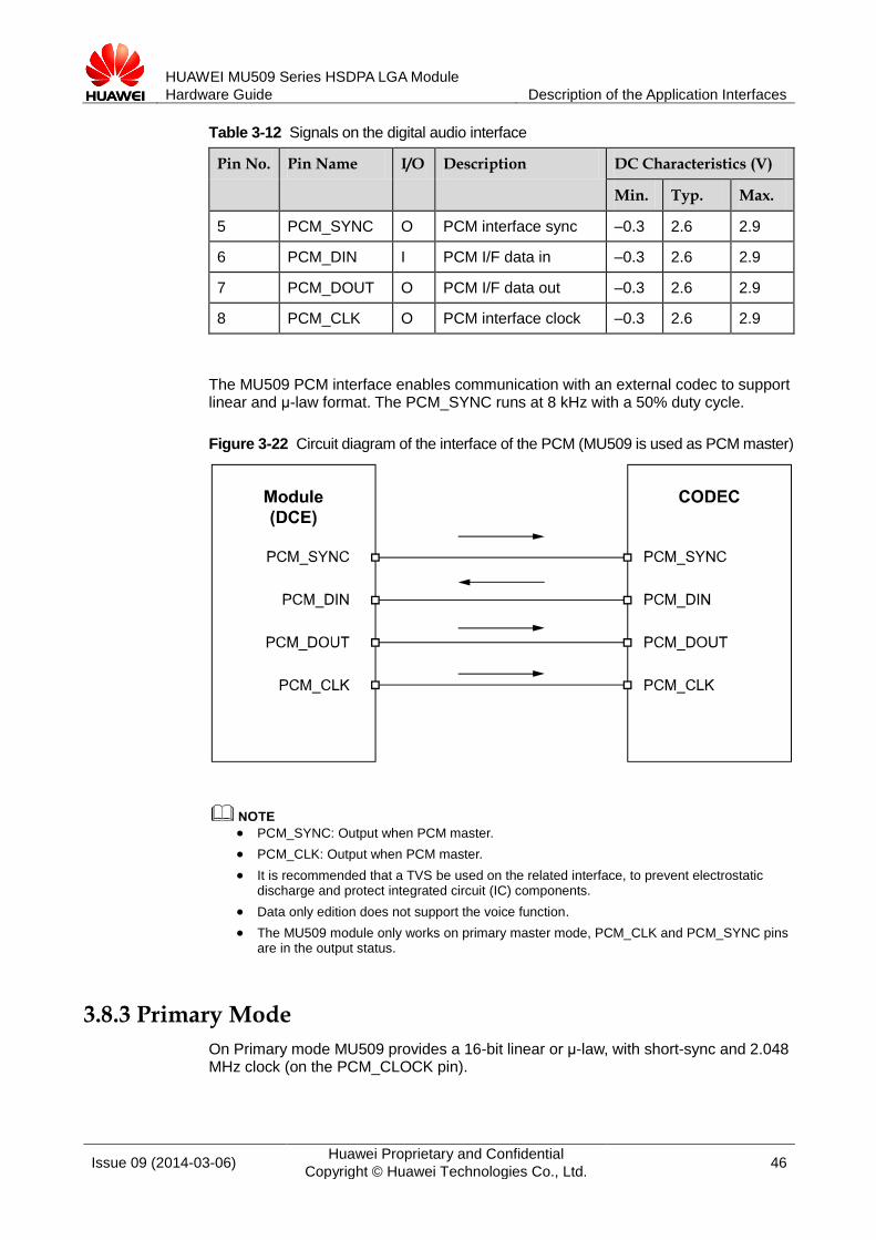
Figure 3-22 Circuit diagram of the interface of the PCM (MU509 is used as PCM master)
PCM_SYNC: Output when PCM master.
PCM_CLK: Output when PCM master.
It is recommended that a TVS be used on the related interface, to prevent electrostatic discharge and protect integrated circuit (IC) components.
Data only edition does not support the voice function.
The MU509 module only works on primary master mode, PCM_CLK and PCM_SYNC pins are in the output status.
3.8.3 Primary Mode
On Primary mode MU509 provides a 16-bit linear or μ-law, with short-sync and 2.048 MHz clock (on the PCM_CLOCK pin).

HUAWEI MU509 Series HSDPA LGA Module Hardware Guide Description of the Application Interfaces
Issue 09 (2014-03-06) Huawei Proprietary and Confidential Copyright © Huawei Technologies Co., Ltd. 47
3.9 General Purpose I/O Interface The LGA module provides 8 channels GPIO pins for customers to use controlling signals which are worked at 2.6 V CMOS logic levels. Customers can use AT command to control the state of logic levels of eight channels GPIO output signal. For MU509-b, MU509-g and HUAWEI MU509-1, see the HUAWEI MU509 HSDPA LGA Module AT Command Interface Specification. For MU509-c, see the HUAWEI MU509-c HSDPA LGA Module AT Command Interface Specification.
Table 3-13 Signals on the GPIO interface
Pin No. Pin Name
I/O Description DC Characteristics (V)
Min. Typ. Max.
44, 45, 46, 51, 55, 105, 109, 113
GPIO I/O General I/O pins
–0.3 2.6 2.9
3.10 JTAG Interface The MU509 module provides one JTAG interface (Joint Test Action Group). It is suggested that place the follow test points in the DTE board for debug. It is recommended that set the 9 pins related to JTAG interface as test points on the DTE for tracing and debugging.
Table 3-14 Signals on the JTAG interface
Pin No. Pin Name I/O Description DC Characteristics (V)
Min. Typ. Max.
30 JTAG_TMS I JTAG Test mode select –0.3 1.8 2.1
36 JTAG_TRST_N I JTAG reset. –0.3 1.8 2.1
42 JTAG_TCK I JTAG clock input –0.3 1.8 2.1
72 JTAG_TDO O JTAG test data output –0.3 1.8 2.1
87 JTAG_TDI I JTAG test data input –0.3 1.8 2.1
93 JTAG_RTCK O JTAG return clock –0.3 1.8 2.1
14 PS_HOLD I This input high to keep power on, low to shut down.
- 1.8 -
32 VCC_EXT1 P 1.8 V POWER output - 1.8 -

HUAWEI MU509 Series HSDPA LGA Module Hardware Guide Description of the Application Interfaces
Issue 09 (2014-03-06) Huawei Proprietary and Confidential Copyright © Huawei Technologies Co., Ltd. 48
Pin No. Pin Name I/O Description DC Characteristics (V)
Min. Typ. Max.
100 RESIN_N I Reset module. –0.3 1.8 2.1
3.11 RF Antenna Interface The MU509 module provides an RF antenna pad for connecting an external antenna. Through the MAIN_ANT pad, the antenna interface is routed to the coaxial connector on the DTE (for impedance 50 Ω).The external antenna is connected to the module through the coaxial connector.
A matching location for the antenna must be reserved at the antenna port.
Table 3-15 Signals on RF Antenna pad
Pin No. Pin Name I/O Description
107 MAIN_ANT - RF main antenna pad
3.12 NC Pins The LGA module have 47 NC pins, All of NC interface should not be connected. Please keep these pins open.
Table 3-16 Signals on NC interface
Pin No. Pin Name I/O Description
1–4, 9, 10, 16–27, 33, 37, 47, 60–70, 82–84, 92, 94, 95, 102–104, 111, 115, 117–120
NC - Not connected, please keep this pin open.
HUAWEI MU509 Series HSDPA LGA Module Hardware Guide RF Specifications
Issue 09 (2014-03-06) Huawei Proprietary and Confidential Copyright © Huawei Technologies Co., Ltd. 49
4 RF Specifications
4.1 About This Chapter This chapter describes the RF specifications of the MU509 module, including:
Antenna Installation Guidelines Operating Frequencies Conducted RF Measurement Conducted Rx Sensitivity and Tx Power Antenna Design Requirements
4.2 Antenna Installation Guidelines Install the antenna in a place covered by the signal. The Antenna must be installed to provide a separation distance of at least 20 cm
from all persons and must not be co-located or operating in conjunction with any other antenna or transmitter.
Antenna must not be installed inside metal cases. Antenna must be installed also according Antenna manufacturer instructions.
4.3 Operating Frequencies Table 4-1 shows the RF bands supported by MU509.
Table 4-1 RF bands
Operating Band Tx Rx
UMTS 2100 (Band I) 1920 MHz–1980 MHz 2110 MHz–2170 MHz
UMTS 1900 (Band II) 1850 MHz–1910 MHz 1930 MHz–1990 MHz
UMTS 900 (Band VIII) 880 MHz–915 MHz 925 MHz–960 MHz
UMTS 850 (Band V) 824 MHz–849 MHz 869 MHz–894 MHz

HUAWEI MU509 Series HSDPA LGA Module Hardware Guide RF Specifications
Issue 09 (2014-03-06) Huawei Proprietary and Confidential Copyright © Huawei Technologies Co., Ltd. 50
Operating Band Tx Rx
GSM 850 824 MHz–849 MHz 869 MHz–894 MHz
GSM 900 880 MHz–915 MHz 925 MHz–960 MHz
GSM 1800 (DCS) 1710 MHz–1785 MHz 1805 MHz–1880 MHz
GSM 1900 (PCS) 1850 MHz–1910 MHz 1930 MHz–1990 MHz
4.4 Conducted RF Measurement 4.4.1 Test Environment
Test instrument R&S CMU200
Power supply KEITHLEY 2306
RF cable for testing
L08-C014-350 of DRAKA COMTEQ or Rosenberger Cable length: 29 cm Compensation for 850 MHz or 900 MHz: 0.6 dB Compensation for 2100 MHz, 1900MHz or 1800 MHz: 0.8 dB
The compensation for different frequency bands relates to the cable and the test
environment. The instrument compensation needs to be set according to the actual cable conditions.
4.4.2 Test Standards Huawei modules meet all 3GPP test standards relating to both 2G and 3G. Each module passes strict tests at the factory and thus the quality of the modules is guaranteed.
4.5 Conducted Rx Sensitivity and Tx Power 4.5.1 Conducted Receive Sensitivity
The conducted receive sensitivity is a key parameter that indicates the receiver performance of MU509.
The 3GPP Protocol Claim column in Table 4-2 lists the required minimum values, and the Test Value column lists the tested values of MU509.

HUAWEI MU509 Series HSDPA LGA Module Hardware Guide RF Specifications
Issue 09 (2014-03-06) Huawei Proprietary and Confidential Copyright © Huawei Technologies Co., Ltd. 51
Table 4-2 MU509 conducted Rx sensitivity
Item 3GPP Protocol Claim (dBm)
MU509 Test Value (dBm)
Min. Typ. Max
GSM850 GMSK (BER < 2.43%) < –102 - –109 –106
8PSK (MCS5, BLER < 10%)
< –98 - –103 –100
GSM900 GMSK (BER < 2.43%) < –102 - –109 –106
8PSK (MCS5, BLER < 10%)
< –98 - –103 –100
GSM1800 GMSK (BER < 2.43%) < –102 - –109 –106
8PSK (MCS5, BLER < 10%)
< –98 - –103 –100
GSM1900 GMSK (BER < 2.43%) < –102 - –109 –106
8PSK (MCS5, BLER < 10%)
< –98 - –103 –100
BandI (BER < 0.1%) < –106.7 - –110 –107
BandII (BER < 0.1%) < –104.7 - –108.5 –106.5
Band VIII (BER < 0.1%) < –103.7 - –110 –107
Band V (BER < 0.1%) < –104.7 - –110 –107
The test values are the average of some test samples.
4.5.2 Conducted Transmit Power The conducted transmit power is another indicator that measures the performance of MU509. The conducted transmit power refers to the maximum power that the module tested at the antenna port can transmit. According to the 3GPP protocol, the required transmit power varies with the power class.
Table 4-3 lists the required ranges of the conducted transmit power of MU509. The tested values listed in the Test Value column must range from the minimum power to the maximum power.
Table 4-3 MU509 conducted Tx power
Item 3GPP Protocol Claim (dBm)
MU509 Test Value (dBm)
Min. Typ. Max.
GSM850 GMSK(1Tx Slot) 31–35 31 32.5 34
HUAWEI MU509 Series HSDPA LGA Module Hardware Guide RF Specifications
Issue 09 (2014-03-06) Huawei Proprietary and Confidential Copyright © Huawei Technologies Co., Ltd. 52
Item 3GPP Protocol Claim (dBm)
MU509 Test Value (dBm)
Min. Typ. Max.
8PSK(1Tx Slot) 24–30 25.5 27 28.5
GSM900 GMSK(1Tx Slot) 31–35 31 32.5 34
8PSK(1Tx Slot) 24–30 25.5 27 28.5
GSM1800 GMSK(1Tx Slot) 28–32 28 29.5 31
8PSK(1Tx Slot) 23–29 24.5 26 27.5
GSM1900 GMSK(1Tx Slot) 28–32 28 29.5 31
8PSK(1Tx Slot) 23–29 24.5 26 27.5
Band I(W2100) 21–25 21.5 23 24.5
Band II(W1900) 21–25 21.5 23 24.5
Band VIII(W900) 21–25 21.5 23 24.5
Band V(W850) 21–25 21.5 23 24 .5
4.6 Antenna Design Requirements 4.6.1 Antenna Design Indicators
Antenna Efficiency Antenna efficiency is the ratio of the input power to the radiated or received power of an antenna. The radiated power of an antenna is always lower than the input power due to the following antenna losses: return loss, material loss, and coupling loss. The efficiency of an antenna relates to its electrical dimensions. To be specific, the antenna efficiency increases with the electrical dimensions. In addition, the transmission cable from the antenna port of MU509 to the antenna is also part of the antenna. The cable loss increases with the cable length and the frequency. It is recommended that the cable loss be as low as possible, for example, U.FL-LP-088 made by HRS.
The following antenna efficiency (free space) is recommended for MU509 to ensure high radio performance of the module: Efficiency of the master antenna: ≥ 40% (below 960 MHz); ≥ 50% (over 1710 MHz). In addition, the efficiency should be tested with the transmission cable.
S11 or VSWR S11 indicates the degree to which the input impedance of an antenna matches the reference impedance (50 Ω). S11 shows the resonance feature and impedance bandwidth of an antenna. Voltage standing wave ratio (VSWR) is another expression
HUAWEI MU509 Series HSDPA LGA Module Hardware Guide RF Specifications
Issue 09 (2014-03-06) Huawei Proprietary and Confidential Copyright © Huawei Technologies Co., Ltd. 53
of S11. S11 relates to the antenna efficiency. S11 can be measured with a vector analyzer.
The following S11 values are recommended for the antenna of MU509: S11 of the master antenna ≤ –6 dB.
Polarization The polarization of an antenna is the orientation of the electric field vector that rotates with time in the direction of maximum radiation.
The linear polarization is recommended for the antenna of MU509.
Radiation Pattern The radiation pattern of an antenna reflects the radiation features of the antenna in the remote field region. The radiation pattern of an antenna commonly describes the power or field strength of the radiated electromagnetic waves in various directions from the antenna. The power or field strength varies with the angular coordinates (θ and φ), but is independent of the radial coordinates.
The radiation pattern of half wave dipole antennas is omnidirectional in the horizontal plane, and the incident waves of base stations are often in the horizontal plane. For this reason, the receiving performance is optimal.
The following radiation patterns are recommended for the antenna of MU509. Master antenna: omnidirectional.
Gain and Directivity The radiation pattern of an antenna represents the field strength of the radiated electromagnetic waves in all directions, but not the power density that the antenna radiates in the specific direction. The directivity of an antenna, however, measures the power density that the antenna radiates.
Gain, as another important parameter of antennas, correlates closely to the directivity. The gain of an antenna takes both the directivity and the efficiency of the antenna into account. The appropriate antenna gain prolongs the service life of relevant batteries.
The following antenna gain is recommended for MU509. Gain of the master antenna ≤ 2.5 dBi.
The antenna consists of the antenna body and the relevant RF transmission cable. Take the
RF transmission cable into account when measuring any of the preceding antenna indicators.
Huawei cooperates with various famous antenna suppliers who are able to make suggestions on antenna design, for example, Amphenol, Skycross, etc.
4.6.2 Interference Besides the antenna performance, the interference on the user board also affects the radio performance (especially the TIS) of the module. To guarantee high performance of the module, the interference sources on the user board must be properly controlled.
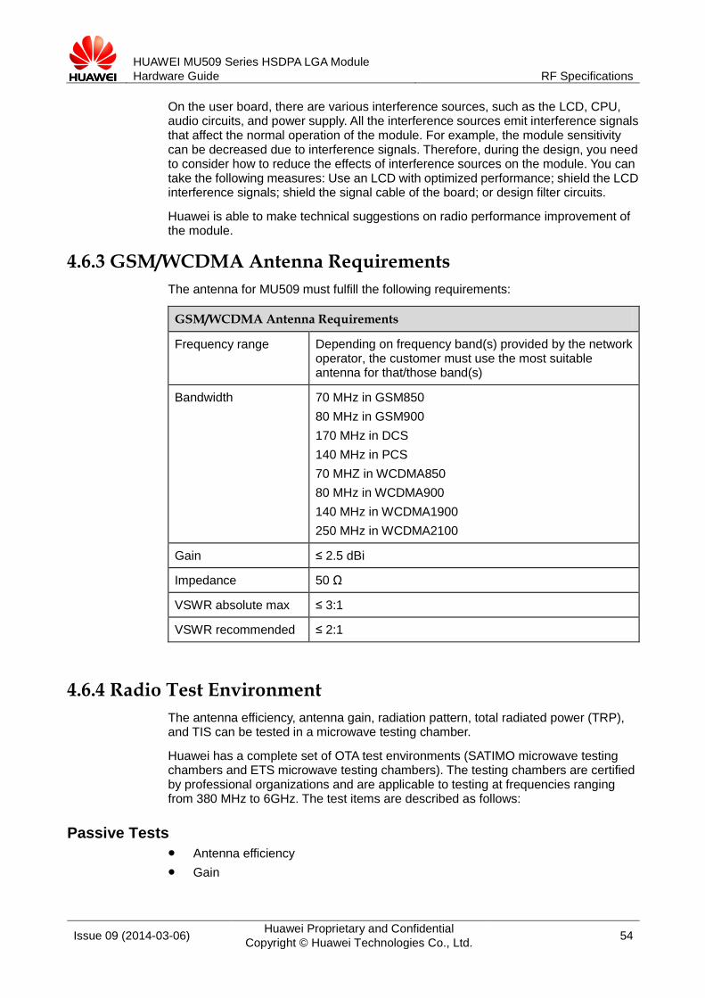
HUAWEI MU509 Series HSDPA LGA Module Hardware Guide RF Specifications
Issue 09 (2014-03-06) Huawei Proprietary and Confidential Copyright © Huawei Technologies Co., Ltd. 54
On the user board, there are various interference sources, such as the LCD, CPU, audio circuits, and power supply. All the interference sources emit interference signals that affect the normal operation of the module. For example, the module sensitivity can be decreased due to interference signals. Therefore, during the design, you need to consider how to reduce the effects of interference sources on the module. You can take the following measures: Use an LCD with optimized performance; shield the LCD interference signals; shield the signal cable of the board; or design filter circuits.
Huawei is able to make technical suggestions on radio performance improvement of the module.
4.6.3 GSM/WCDMA Antenna Requirements The antenna for MU509 must fulfill the following requirements:
GSM/WCDMA Antenna Requirements
Frequency range Depending on frequency band(s) provided by the network operator, the customer must use the most suitable antenna for that/those band(s)
Bandwidth 70 MHz in GSM850 80 MHz in GSM900 170 MHz in DCS 140 MHz in PCS 70 MHZ in WCDMA850 80 MHz in WCDMA900 140 MHz in WCDMA1900 250 MHz in WCDMA2100
Gain ≤ 2.5 dBi
Impedance 50 Ω
VSWR absolute max ≤ 3:1
VSWR recommended ≤ 2:1
4.6.4 Radio Test Environment The antenna efficiency, antenna gain, radiation pattern, total radiated power (TRP), and TIS can be tested in a microwave testing chamber.
Huawei has a complete set of OTA test environments (SATIMO microwave testing chambers and ETS microwave testing chambers). The testing chambers are certified by professional organizations and are applicable to testing at frequencies ranging from 380 MHz to 6GHz. The test items are described as follows:
Passive Tests Antenna efficiency Gain
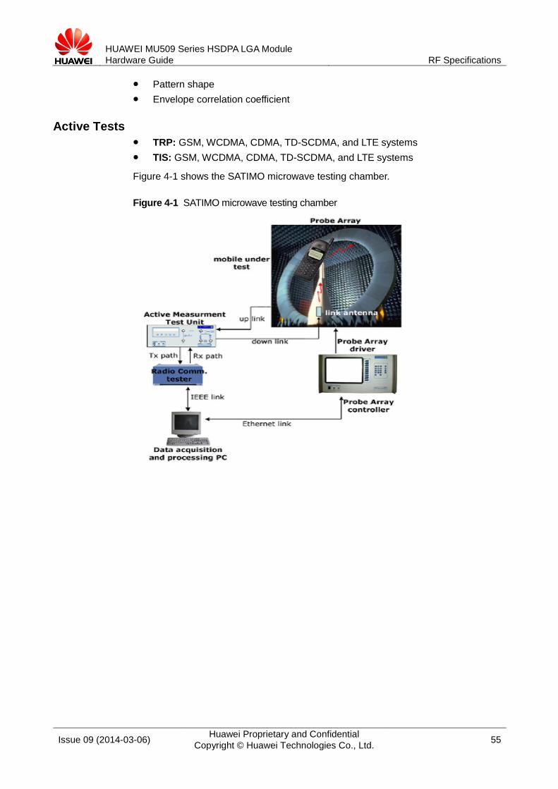
HUAWEI MU509 Series HSDPA LGA Module Hardware Guide RF Specifications
Issue 09 (2014-03-06) Huawei Proprietary and Confidential Copyright © Huawei Technologies Co., Ltd. 55
Pattern shape Envelope correlation coefficient
Active Tests TRP: GSM, WCDMA, CDMA, TD-SCDMA, and LTE systems TIS: GSM, WCDMA, CDMA, TD-SCDMA, and LTE systems
Figure 4-1 shows the SATIMO microwave testing chamber.
Figure 4-1 SATIMO microwave testing chamber
HUAWEI MU509 Series HSDPA LGA Module Hardware Guide Electrical and Reliability Features
Issue 09 (2014-03-06) Huawei Proprietary and Confidential Copyright © Huawei Technologies Co., Ltd. 56
5 Electrical and Reliability Features
5.1 About This Chapter This chapter describes the electrical and reliability features of the interfaces in the MU509 module, including:
Extreme Operating Conditions Operating and Storage Temperatures and Humidity Electrical Features of Application Interfaces Power Supply Features Reliability Features EMC and ESD Features
5.2 Extreme Operating Conditions
Table 5-1 lists the extreme operating conditions for the MU509 module. Using the MU509 module beyond these conditions may result in permanent damage to the module.
Table 5-1 Extreme working conditions for the MU509 module
Symbol Specification Minimum Value
Maximum Value
Unit
VBAT External power voltage –0.4 5.0 V
VCOIN Input voltage of standby power for the RTC
1.5 3.25 V
VI Data pin voltage –0.3 VI+0.3 V
HUAWEI MU509 Series HSDPA LGA Module Hardware Guide Electrical and Reliability Features
Issue 09 (2014-03-06) Huawei Proprietary and Confidential Copyright © Huawei Technologies Co., Ltd. 57
VI is 2.6 V or 1.8 V. To get the details about the voltage of VI, please refer to Table 3-1 .
5.3 Operating and Storage Temperatures and Humidity Table 5-2 lists the operating and storage temperatures and humidity for the MU509 module.
Table 5-2 operating and storage temperatures and humidity for the MU509 module
Specification Minimum Value Maximum Value Unit
Normal working temperatures[1] –20 +70 °C
Extended working temperatures –40 –20 °C
Extended working temperatures +70 +85 °C
Ambient temperature for storage
–40 +85 °C
Moisture 5 95 %
[1]: The temperatures outside of the range –20°C to +70°C; the module might slightly deviate from 3GPP TS 45.005 and 3GPP TS 34.121-1 specifications.
5.4 Electrical Features of Application Interfaces Table 5-3 lists electrical features (typical values).
Table 5-3 Electrical features of application interfaces
Parameter Description Minimum Value Maximum Value Unit
VIH High-level input voltage
0.65 x VDD_PX VDD_PX + 0.3 V
VIL Low-level input voltage
–0.3 0.35 x VDD_PX V
Ileak Input leakage current
–0.2 0.2 μA
VOH High-level output voltage
VDD_PX – 0.45 VDD_PX V

HUAWEI MU509 Series HSDPA LGA Module Hardware Guide Electrical and Reliability Features
Issue 09 (2014-03-06) Huawei Proprietary and Confidential Copyright © Huawei Technologies Co., Ltd. 58
Parameter Description Minimum Value Maximum Value Unit
VOL Low-level output voltage
0 0.45 V
IOH High-level output current
1.5 - mA
IOL Low-level output current
- –1.5 mA
VDD_PX is 2.6 V or 1.8 V. To get the details about the voltage of VDD_PX, please refer to Table 3-1 .
5.5 Power Supply Features 5.5.1 Input Power Supply
Table 5-4 lists the requirements for input power of the MU509 module.
Table 5-4 Requirements for input power of the MU509 module
Parameter Minimum Value
Typical Value
Maximum Value
Ripple Unit
VBAT 3.3 3.8 4.2 < 50 mVpp (0 Hz to 2.5 GHz)
V
VCOIN 1.5 3.0 3.25 < 30 mVpp V
Figure 5-1 Power Supply During Burst Emission
The VBAT Minimum Value must be guaranteed during the burst (with 2.75 A Peak in GSM, GPRS or EGPRS mode).
VBATVoltage Signal
TX BurstTiming Sequence
Ripple Ripple
VBAT
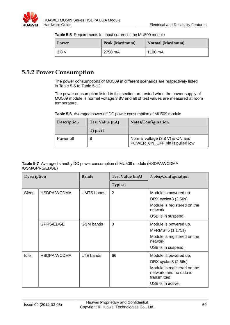
HUAWEI MU509 Series HSDPA LGA Module Hardware Guide Electrical and Reliability Features
Issue 09 (2014-03-06) Huawei Proprietary and Confidential Copyright © Huawei Technologies Co., Ltd. 59
Table 5-5 Requirements for input current of the MU509 module
Power Peak (Maximum) Normal (Maximum)
3.8 V 2750 mA 1100 mA
5.5.2 Power Consumption The power consumptions of MU509 in different scenarios are respectively listed in Table 5-6 to Table 5-12 .
The power consumption listed in this section are tested when the power supply of MU509 module is normal voltage 3.8V and all of test values are measured at room temperature.
Table 5-6 Averaged power off DC power consumption of MU509 module
Description Test Value (uA) Notes/Configuration
Typical
Power off 8 Normal voltage (3.8 V) is ON and POWER_ON_OFF pin is pulled low
Table 5-7 Averaged standby DC power consumption of MU509 module (HSDPA/WCDMA /GSM/GPRS/EDGE)
Description Bands Test Value (mA) Notes/Configuration
Typical
Sleep HSDPA/WCDMA UMTS bands 2 Module is powered up. DRX cycle=8 (2.56s) Module is registered on the network. USB is in suspend.
GPRS/EDGE GSM bands 3 Module is powered up. MFRMS=5 (1.175s) Module is registered on the network. USB is in suspend.
Idle HSDPA/WCDMA LTE bands 66 Module is powered up. DRX cycle=8 (2.56s) Module is registered on the network, and no data is transmitted. USB is in active.
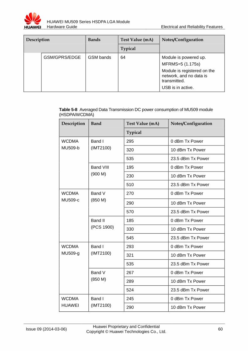
HUAWEI MU509 Series HSDPA LGA Module Hardware Guide Electrical and Reliability Features
Issue 09 (2014-03-06) Huawei Proprietary and Confidential Copyright © Huawei Technologies Co., Ltd. 60
Description Bands Test Value (mA) Notes/Configuration
Typical
GSM/GPRS/EDGE GSM bands 64 Module is powered up. MFRMS=5 (1.175s) Module is registered on the network, and no data is transmitted. USB is in active.
Table 5-8 Averaged Data Transmission DC power consumption of MU509 module (HSDPA/WCDMA)
Description Band Test Value (mA) Notes/Configuration
Typical
WCDMA MU509-b
Band I (IMT2100)
295 0 dBm Tx Power
320 10 dBm Tx Power
535 23.5 dBm Tx Power
Band VIII (900 M)
195 0 dBm Tx Power
230 10 dBm Tx Power
510 23.5 dBm Tx Power
WCDMA MU509-c
Band V (850 M)
270 0 dBm Tx Power
290 10 dBm Tx Power
570 23.5 dBm Tx Power
Band II (PCS 1900)
185 0 dBm Tx Power
330 10 dBm Tx Power
545 23.5 dBm Tx Power
WCDMA MU509-g
Band I (IMT2100)
293 0 dBm Tx Power
321 10 dBm Tx Power
535 23.5 dBm Tx Power
Band V (850 M)
267 0 dBm Tx Power
289 10 dBm Tx Power
524 23.5 dBm Tx Power
WCDMA HUAWEI
Band I (IMT2100)
245 0 dBm Tx Power
290 10 dBm Tx Power

HUAWEI MU509 Series HSDPA LGA Module Hardware Guide Electrical and Reliability Features
Issue 09 (2014-03-06) Huawei Proprietary and Confidential Copyright © Huawei Technologies Co., Ltd. 61
Description Band Test Value (mA) Notes/Configuration
Typical MU509-1 585 23.5 dBm Tx Power
HSDPA MU509-b
Band I (IMT2100)
310 0 dBm Tx Power
340 10 dBm Tx Power
550 23.5 dBm Tx Power
Band VIII (900 M)
215 0 dBm Tx Power
305 10 dBm Tx Power
510 23.5 dBm Tx Power
HSDPA MU509-c
Band V (850 M)
285 0 dBm Tx Power
315 10 dBm Tx Power
540 23.5 dBm Tx Power
Band II (PCS 1900)
195 0 dBm Tx Power
340 10 dBm Tx Power
520 23.5 dBm Tx Power
HSDPA MU509-g
Band I (IMT2100)
311 0 dBm Tx Power
338 10 dBm Tx Power
549 23.5 dBm Tx Power
Band V (850 M)
301 0 dBm Tx Power
328 10 dBm Tx Power
598 23.5 dBm Tx Power
HSDPA HUAWEI MU509-1
Band I (IMT2100)
260 0 dBm Tx Power
320 10 dBm Tx Power
585 23.5 dBm Tx Power
Table 5-9 Averaged DC power consumption of MU509-b (GPRS/EDGE)
Description Test Value (mA) PCL Notes/Configuration
Typical
GPRS850 310 5 1 Up/1 Down
470 2 Up/1 Down
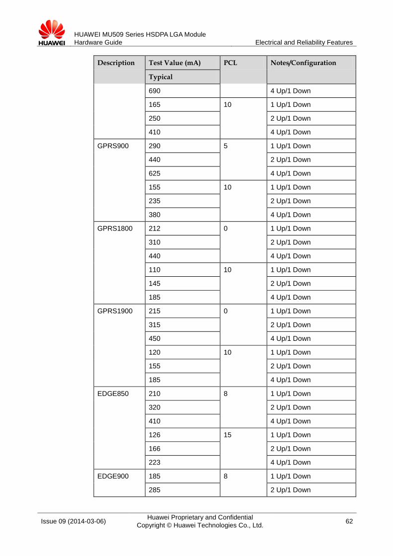
HUAWEI MU509 Series HSDPA LGA Module Hardware Guide Electrical and Reliability Features
Issue 09 (2014-03-06) Huawei Proprietary and Confidential Copyright © Huawei Technologies Co., Ltd. 62
Description Test Value (mA) PCL Notes/Configuration
Typical
690 4 Up/1 Down
165 10 1 Up/1 Down
250 2 Up/1 Down
410 4 Up/1 Down
GPRS900 290 5 1 Up/1 Down
440 2 Up/1 Down
625 4 Up/1 Down
155 10 1 Up/1 Down
235 2 Up/1 Down
380 4 Up/1 Down
GPRS1800 212 0 1 Up/1 Down
310 2 Up/1 Down
440 4 Up/1 Down
110 10 1 Up/1 Down
145 2 Up/1 Down
185 4 Up/1 Down
GPRS1900 215 0 1 Up/1 Down
315 2 Up/1 Down
450 4 Up/1 Down
120 10 1 Up/1 Down
155 2 Up/1 Down
185 4 Up/1 Down
EDGE850 210 8 1 Up/1 Down
320 2 Up/1 Down
410 4 Up/1 Down
126 15 1 Up/1 Down
166 2 Up/1 Down
223 4 Up/1 Down
EDGE900 185 8 1 Up/1 Down
285 2 Up/1 Down
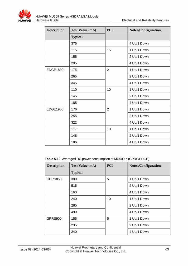
HUAWEI MU509 Series HSDPA LGA Module Hardware Guide Electrical and Reliability Features
Issue 09 (2014-03-06) Huawei Proprietary and Confidential Copyright © Huawei Technologies Co., Ltd. 63
Description Test Value (mA) PCL Notes/Configuration
Typical
375 4 Up/1 Down
115 15 1 Up/1 Down
155 2 Up/1 Down
205 4 Up/1 Down
EDGE1800 175 2 1 Up/1 Down
265 2 Up/1 Down
345 4 Up/1 Down
110 10 1 Up/1 Down
145 2 Up/1 Down
185 4 Up/1 Down
EDGE1900 176 2 1 Up/1 Down
255 2 Up/1 Down
322 4 Up/1 Down
117 10 1 Up/1 Down
148 2 Up/1 Down
186 4 Up/1 Down
Table 5-10 Averaged DC power consumption of MU509-c (GPRS/EDGE)
Description Test Value (mA) PCL Notes/Configuration
Typical
GPRS850 300 5 1 Up/1 Down
515 2 Up/1 Down
160 4 Up/1 Down
240 10 1 Up/1 Down
285 2 Up/1 Down
490 4 Up/1 Down
GPRS900 155 5 1 Up/1 Down
235 2 Up/1 Down
240 4 Up/1 Down

HUAWEI MU509 Series HSDPA LGA Module Hardware Guide Electrical and Reliability Features
Issue 09 (2014-03-06) Huawei Proprietary and Confidential Copyright © Huawei Technologies Co., Ltd. 64
Description Test Value (mA) PCL Notes/Configuration
Typical
395 10 1 Up/1 Down
115 2 Up/1 Down
150 4 Up/1 Down
GPRS1800 230 0 1 Up/1 Down
365 2 Up/1 Down
125 4 Up/1 Down
160 10 1 Up/1 Down
195 2 Up/1 Down
310 4 Up/1 Down
GPRS1900 515 0 1 Up/1 Down
115 2 Up/1 Down
155 4 Up/1 Down
210 10 1 Up/1 Down
190 2 Up/1 Down
300 4 Up/1 Down
EDGE850 495 8 1 Up/1 Down
155 2 Up/1 Down
230 4 Up/1 Down
355 15 1 Up/1 Down
185 2 Up/1 Down
290 4 Up/1 Down
EDGE900 475 8 1 Up/1 Down
115 2 Up/1 Down
150 4 Up/1 Down
195 15 1 Up/1 Down
175 2 Up/1 Down
270 4 Up/1 Down
EDGE1800 430 2 1 Up/1 Down
110 2 Up/1 Down
145 4 Up/1 Down

HUAWEI MU509 Series HSDPA LGA Module Hardware Guide Electrical and Reliability Features
Issue 09 (2014-03-06) Huawei Proprietary and Confidential Copyright © Huawei Technologies Co., Ltd. 65
Description Test Value (mA) PCL Notes/Configuration
Typical
190 10 1 Up/1 Down
145 2 Up/1 Down
185 4 Up/1 Down
EDGE1900 176 2 1 Up/1 Down
255 2 Up/1 Down
322 4 Up/1 Down
117 10 1 Up/1 Down
148 2 Up/1 Down
186 4 Up/1 Down
Table 5-11 Averaged DC power consumption of MU509-g (GPRS/EDGE)
Description Test Value (mA) PCL Notes/Configuration
Typical
GPRS850 310 5 1 Up/1 Down
470 2 Up/1 Down
690 4 Up/1 Down
165 10 1 Up/1 Down
250 2 Up/1 Down
410 4 Up/1 Down
GPRS900 290 5 1 Up/1 Down
440 2 Up/1 Down
625 4 Up/1 Down
155 10 1 Up/1 Down
235 2 Up/1 Down
380 4 Up/1 Down
GPRS1800 245 0 1 Up/1 Down
345 2 Up/1 Down
480 4 Up/1 Down
110 10 1 Up/1 Down
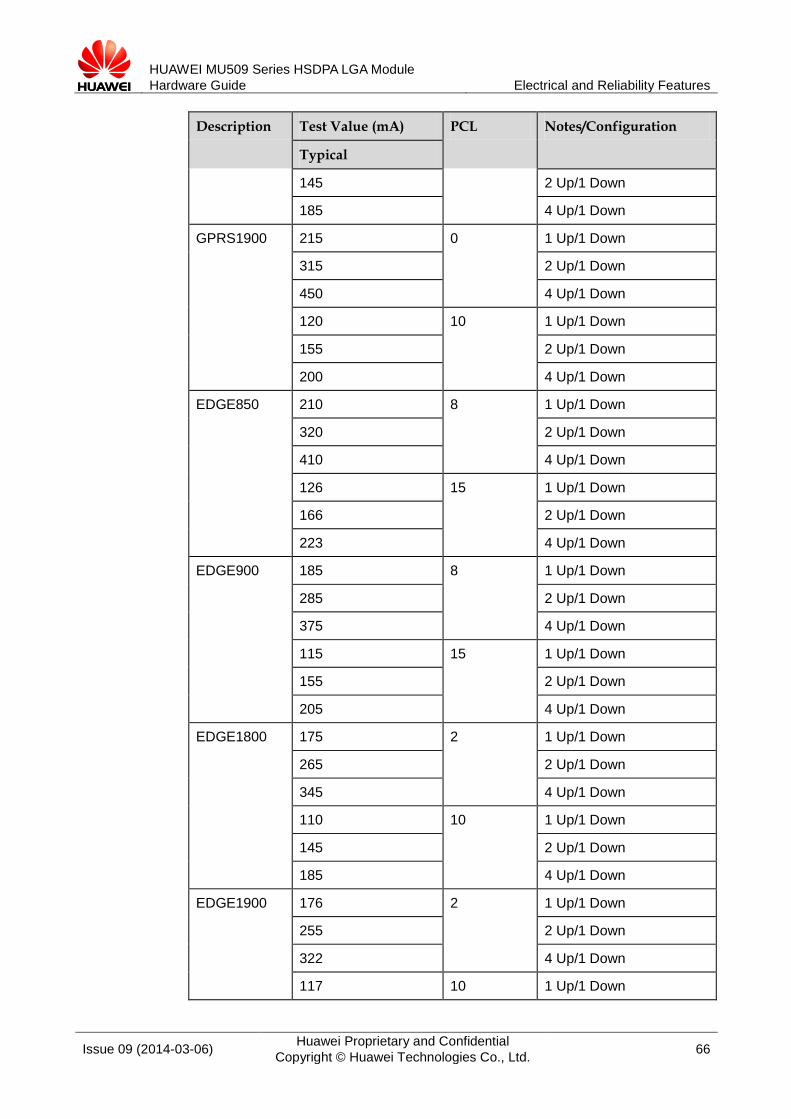
HUAWEI MU509 Series HSDPA LGA Module Hardware Guide Electrical and Reliability Features
Issue 09 (2014-03-06) Huawei Proprietary and Confidential Copyright © Huawei Technologies Co., Ltd. 66
Description Test Value (mA) PCL Notes/Configuration
Typical
145 2 Up/1 Down
185 4 Up/1 Down
GPRS1900 215 0 1 Up/1 Down
315 2 Up/1 Down
450 4 Up/1 Down
120 10 1 Up/1 Down
155 2 Up/1 Down
200 4 Up/1 Down
EDGE850 210 8 1 Up/1 Down
320 2 Up/1 Down
410 4 Up/1 Down
126 15 1 Up/1 Down
166 2 Up/1 Down
223 4 Up/1 Down
EDGE900 185 8 1 Up/1 Down
285 2 Up/1 Down
375 4 Up/1 Down
115 15 1 Up/1 Down
155 2 Up/1 Down
205 4 Up/1 Down
EDGE1800 175 2 1 Up/1 Down
265 2 Up/1 Down
345 4 Up/1 Down
110 10 1 Up/1 Down
145 2 Up/1 Down
185 4 Up/1 Down
EDGE1900 176 2 1 Up/1 Down
255 2 Up/1 Down
322 4 Up/1 Down
117 10 1 Up/1 Down
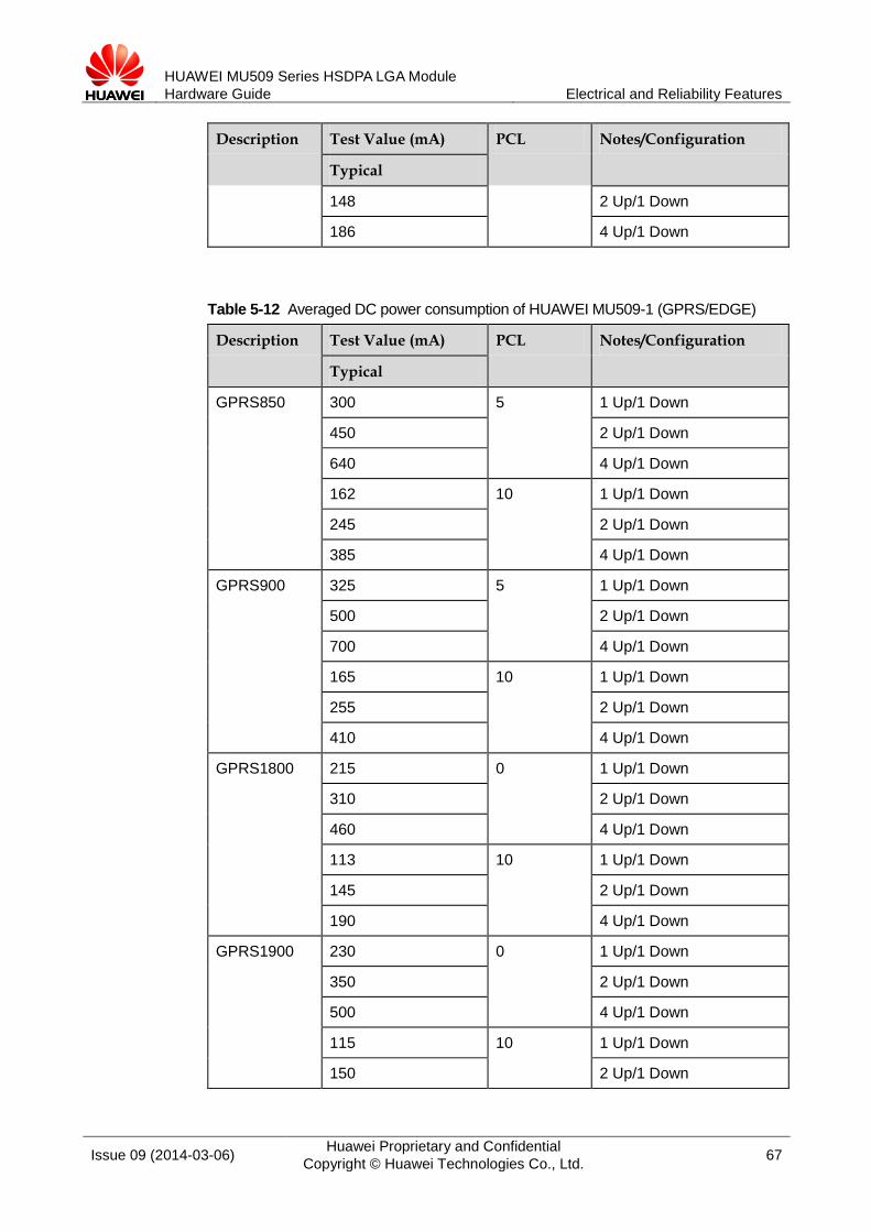
HUAWEI MU509 Series HSDPA LGA Module Hardware Guide Electrical and Reliability Features
Issue 09 (2014-03-06) Huawei Proprietary and Confidential Copyright © Huawei Technologies Co., Ltd. 67
Description Test Value (mA) PCL Notes/Configuration
Typical
148 2 Up/1 Down
186 4 Up/1 Down
Table 5-12 Averaged DC power consumption of HUAWEI MU509-1 (GPRS/EDGE)
Description Test Value (mA) PCL Notes/Configuration
Typical
GPRS850 300 5 1 Up/1 Down
450 2 Up/1 Down
640 4 Up/1 Down
162 10 1 Up/1 Down
245 2 Up/1 Down
385 4 Up/1 Down
GPRS900 325 5 1 Up/1 Down
500 2 Up/1 Down
700 4 Up/1 Down
165 10 1 Up/1 Down
255 2 Up/1 Down
410 4 Up/1 Down
GPRS1800 215 0 1 Up/1 Down
310 2 Up/1 Down
460 4 Up/1 Down
113 10 1 Up/1 Down
145 2 Up/1 Down
190 4 Up/1 Down
GPRS1900 230 0 1 Up/1 Down
350 2 Up/1 Down
500 4 Up/1 Down
115 10 1 Up/1 Down
150 2 Up/1 Down
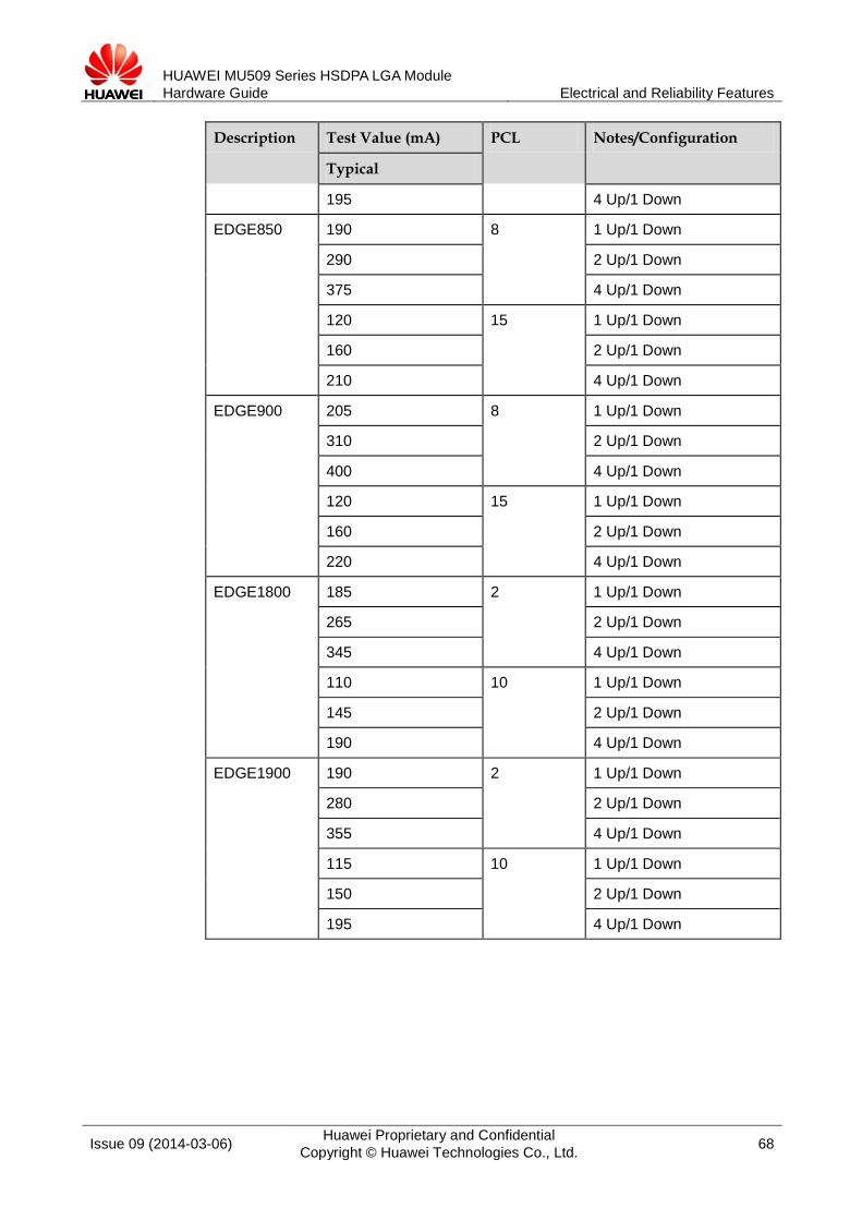
HUAWEI MU509 Series HSDPA LGA Module Hardware Guide Electrical and Reliability Features
Issue 09 (2014-03-06) Huawei Proprietary and Confidential Copyright © Huawei Technologies Co., Ltd. 68
Description Test Value (mA) PCL Notes/Configuration
Typical
195 4 Up/1 Down
EDGE850 190 8 1 Up/1 Down
290 2 Up/1 Down
375 4 Up/1 Down
120 15 1 Up/1 Down
160 2 Up/1 Down
210 4 Up/1 Down
EDGE900 205 8 1 Up/1 Down
310 2 Up/1 Down
400 4 Up/1 Down
120 15 1 Up/1 Down
160 2 Up/1 Down
220 4 Up/1 Down
EDGE1800 185 2 1 Up/1 Down
265 2 Up/1 Down
345 4 Up/1 Down
110 10 1 Up/1 Down
145 2 Up/1 Down
190 4 Up/1 Down
EDGE1900 190 2 1 Up/1 Down
280 2 Up/1 Down
355 4 Up/1 Down
115 10 1 Up/1 Down
150 2 Up/1 Down
195 4 Up/1 Down

HUAWEI MU509 Series HSDPA LGA Module Hardware Guide Electrical and Reliability Features
Issue 09 (2014-03-06) Huawei Proprietary and Confidential Copyright © Huawei Technologies Co., Ltd. 69
All power consumption test configuration can be referenced by GSM Association Official Document TS.09: Battery Life Measurement and Current Consumption Technique. Test condition: For max. Tx power, see 4.5.2 Conducted Transmit Power, which are listed
in Table 4-3 ; for max. data throughput, see 2.2 Function Overview, which are listed in Table 2-1 .
5.6 Reliability Features Table 5-13 lists the test conditions and results of the reliability of the MU509 module.
Table 5-13 Test conditions and results of the reliability of the MU509 module
Item Test Condition Standard Sample size
Results
Stress
Low-temperature storage
Temperature: –40ºC Operation mode: no
power, no package Test duration: 24 h
JESD22-A119-C
3 pcs/group Visual inspection: ok Function test: ok RF specification: ok
High-temperature storage
Temperature: 85ºC Operation mode: no
power, no package Test duration: 24 h
JESD22-A103-C
3 pcs/group Visual inspection: ok Function test: ok RF specification: ok
Low-temperature operating
Temperature: –40ºC Operation mode: working
with service connected Test duration: 24 h
IEC60068-2-1
3 pcs/group Visual inspection: ok Function test: ok RF specification: ok
High-temperature operating
Temperature: 85ºC Operation mode: working
with service connected Test duration: 24 h
JESD22-A108-C
3 pcs/group Visual inspection: ok Function test: ok RF specification: ok
Temperature cycle operating
High temperature: 85ºC Low temperature: -40ºC Operation mode: working
with service connected Test duration: 30 cycles;1
h+1h /cycle
JESD22-A105-B
3pcs/group Visual inspection: ok Function test: ok RF specification: ok

HUAWEI MU509 Series HSDPA LGA Module Hardware Guide Electrical and Reliability Features
Issue 09 (2014-03-06) Huawei Proprietary and Confidential Copyright © Huawei Technologies Co., Ltd. 70
Item Test Condition Standard Sample size
Results
Stress
Damp heat cycling
High temperature: 55ºC Low temperature: 25ºC Humidity: 95%±3% Operation mode: working
with service connected Test duration: 6 cycles;
12 h+12 h/cycle
JESD22-A101-B
3 pcs/group Visual inspection: ok Function test: ok RF specification: ok
Thermal shock Low temperature: –40º High temperature: 85ºC Temperature change
interval: < 20s Operation mode: no
power Test duration: 100 cycles;
15 min+15 min/cycle
JESD22-A106-B
3 pcs/group Visual inspection: ok Function test: ok RF specification: ok
Salty fog test Temperature: 35°C Density of the NaCl
solution: 5%±1% Operation mode: no
power, no package Test duration:
Spraying interval: 8 h Exposing period after removing the salty fog environment: 16 h
JESD22-A107-B
3 pcs/group Visual inspection: ok Function test: ok RF specification: ok
Sine vibration Frequency range: 5 Hz to 200 Hz
Acceleration: 1 Grms Frequency scan rate: 0.5
oct/min Operation mode: working
with service connected Test duration: 3 axial
directions. 2 h for each axial direction.
Operation mode: working with service connected
JESD22-B103-B
3 pcs/group Visual inspection: ok Function test: ok RF specification: ok
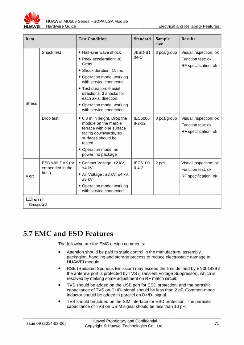
HUAWEI MU509 Series HSDPA LGA Module Hardware Guide Electrical and Reliability Features
Issue 09 (2014-03-06) Huawei Proprietary and Confidential Copyright © Huawei Technologies Co., Ltd. 71
Item Test Condition Standard Sample size
Results
Stress
Shock test Half-sine wave shock Peak acceleration: 30
Grms Shock duration: 11 ms Operation mode: working
with service connected Test duration: 6 axial
directions. 3 shocks for each axial direction.
Operation mode: working with service connected
JESD-B104-C
3 pcs/group Visual inspection: ok Function test: ok RF specification: ok
Drop test 0.8 m in height. Drop the module on the marble terrace with one surface facing downwards, six surfaces should be tested.
Operation mode: no power, no package
IEC60068-2-32
3 pcs/group Visual inspection: ok Function test: ok RF specification: ok
ESD
ESD with DVK (or embedded in the host)
Contact Voltage: ±2 kV, ±4 kV
Air Voltage : ±2 kV, ±4 kV, ±8 kV
Operation mode: working with service connected
IEC61000-4-2
2 pcs Visual inspection: ok Function test: ok RF specification: ok
Groups ≥ 2
5.7 EMC and ESD Features The following are the EMC design comments:
Attention should be paid to static control in the manufacture, assembly, packaging, handling and storage process to reduce electrostatic damage to HUAWEI module.
RSE (Radiated Spurious Emission) may exceed the limit defined by EN301489 if the antenna port is protected by TVS (Transient Voltage Suppressor), which is resolved by making some adjustment on RF match circuit.
TVS should be added on the USB port for ESD protection, and the parasitic capacitance of TVS on D+/D- signal should be less than 2 pF. Common-mode inductor should be added in parallel on D+/D- signal.
TVS should be added on the SIM interface for ESD protection. The parasitic capacitance of TVS on USIM signal should be less than 10 pF;
HUAWEI MU509 Series HSDPA LGA Module Hardware Guide Electrical and Reliability Features
Issue 09 (2014-03-06) Huawei Proprietary and Confidential Copyright © Huawei Technologies Co., Ltd. 72
Resistors in parallel and a 10 nF capacitance should be added on RESIN_N and POWER_ON_OFF signal to avoid shaking, and the distance between the capacitor and the related pins should be less than 100 mil.
PCB routing should be V-type rather than T-type for TVS. An integrated ground plane is necessary for EMC design.
The following are the requirements of ESD environment control:
The electrostatic discharge protected area (EPA) must have an ESD floor whose surface resistance and system resistance are greater than 1 x 10⁴ Ω while less than 1 x 10⁹ Ω.
The EPA must have a sound ground system without loose ground wires, and the ground resistance must be less than 4 Ω.
The workbench for handling ESD sensitive components must be equipped with common ground points, the wrist strap jack, and ESD pad. The resistance between the jack and common ground point must be less than 4 Ω. The surface resistance and system resistance of the ESD pad must be less than 1 x 10⁹ Ω.
The EPA must use the ESD two-circuit wrist strap, and the wrist strap must be connected to the dedicated jack. The crocodile clip must not be connected to the ground.
The ESD sensitive components, the processing equipment, test equipment, tools, and devices must be connected to the ground properly. The indexes are as follows: − Hard ground resistance < 4 Ω − 1 x 10⁵ Ω ≤ Soft ground resistance < 1 x 10⁹ Ω − 1 x 10⁵ Ω ≤ ICT fixture soft ground resistance < 1 x 10¹¹ Ω − The electronic screwdriver and electronic soldering iron can be easily oxidized.
Their ground resistance must be less than 20 Ω. The parts of the equipment, devices, and tools that touch the ESD sensitive
components and moving parts that are close to the ESD sensitive components must be made of ESD materials and have sound ground connection. The parts that are not made of ESD materials must be handled with ESD treatment, such as painting the ESD coating or ionization treatment (check that the friction voltage is less than 100 V).
Key parts in the production equipment (parts that touch the ESD sensitive components or parts that are within 30 cm away from the ESD sensitive components), including the conveyor belt, conveyor chain, guide wheel, and SMT nozzle, must all be made of ESD materials and be connected to the ground properly (check that the friction voltage is less than 100 V).
Engineers that touch IC chips, boards, modules, and other ESD sensitive components and assemblies must wear ESD wrist straps, ESD gloves, or ESD finger cots properly. Engineers that sit when handling the components must all wear ESD wrist straps.
Noticeable ESD warning signs must be attached to the packages and placement areas of ESD sensitive components and assemblies.
Boards and IC chips must not be stacked randomly or be placed with other ESD components.
Effective shielding measures must be taken on the ESD sensitive materials that are transported or stored outside the EPA.

HUAWEI MU509 Series HSDPA LGA Module Hardware Guide Electrical and Reliability Features
Issue 09 (2014-03-06) Huawei Proprietary and Confidential Copyright © Huawei Technologies Co., Ltd. 73
The HUAWEI MU509 module does not include any protection against overvoltage.
HUAWEI MU509 Series HSDPA LGA Module Hardware Guide Process Design
Issue 09 (2014-03-06) Huawei Proprietary and Confidential Copyright © Huawei Technologies Co., Ltd. 74
6 Process Design
6.1 About This Chapter This chapter describes the process design and mechanical specifications:
Storage Requirement Moisture Sensitivity Dimensions and interfaces Packaging Label Customer PCB Design Assembly Processes Specification of Rework
6.2 Storage Requirement The module must be stored and sealed properly in vacuum package under a temperature below 40°C and the relative humidity less than 90% in order to ensure the weldability within 12 months.
6.3 Moisture Sensitivity The moisture sensitivity is level 3. After unpacking, the module must be assembled within 168 hours under the
environmental conditions that the temperature is lower than 30°C and the relative humidity is less than 60%. If the preceding conditions cannot be met, the module needs to be baked according to the parameters specified in Table 6-1 .
Table 6-1 Baking parameters
Baking Temperature Baking Condition Baking Duration Remarks
125°C±5°C Relative humidity ≤ 60% 8 hours -
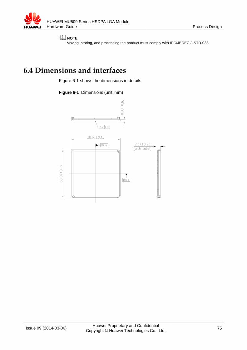
HUAWEI MU509 Series HSDPA LGA Module Hardware Guide Process Design
Issue 09 (2014-03-06) Huawei Proprietary and Confidential Copyright © Huawei Technologies Co., Ltd. 75
Moving, storing, and processing the product must comply with IPC/JEDEC J-STD-033.
6.4 Dimensions and interfaces Figure 6-1 shows the dimensions in details.
Figure 6-1 Dimensions (unit: mm)

HUAWEI MU509 Series HSDPA LGA Module Hardware Guide Process Design
Issue 09 (2014-03-06) Huawei Proprietary and Confidential Copyright © Huawei Technologies Co., Ltd. 76
6.5 Packaging HUAWEI LGA module uses five layers ESD pallet, anti-vibration foam and vacuum packing into cartons.
X
Y
X
Z
323.90
* All30.40 0.10
*All
30.400.10
22.42 0.15
56.0889.74
123.40157.06
190.72
224.38
258.04
291.70
22.20
56.10
90.00
123.90
157.80 *6.60
3.50
1:2
16
6
7
8
9
5
4
10
11
12
13
14
15
17
18
19
20
21
22
ESD PPE
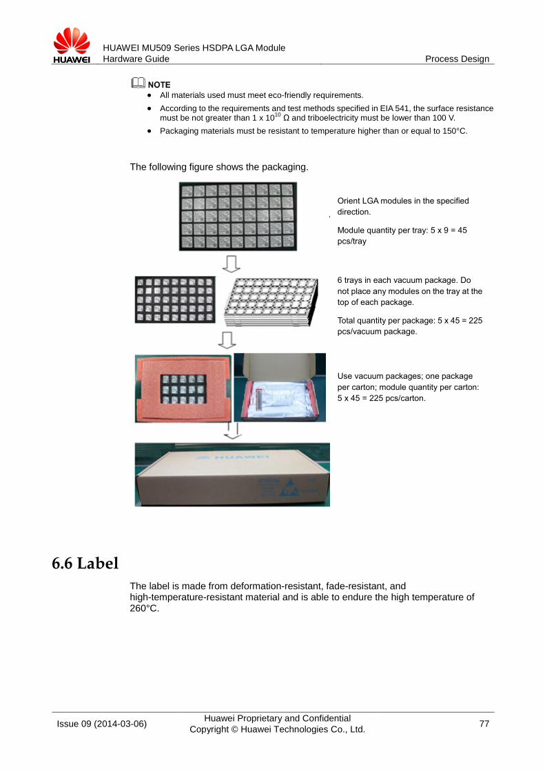
HUAWEI MU509 Series HSDPA LGA Module Hardware Guide Process Design
Issue 09 (2014-03-06) Huawei Proprietary and Confidential Copyright © Huawei Technologies Co., Ltd. 77
All materials used must meet eco-friendly requirements. According to the requirements and test methods specified in EIA 541, the surface resistance
must be not greater than 1 x 10¹⁰ Ω and triboelectricity must be lower than 100 V. Packaging materials must be resistant to temperature higher than or equal to 150°C.
The following figure shows the packaging.
6.6 Label The label is made from deformation-resistant, fade-resistant, and high-temperature-resistant material and is able to endure the high temperature of 260°C.
Orient LGA modules in the specified direction.
Module quantity per tray: 5 x 9 = 45 pcs/tray
6 trays in each vacuum package. Do not place any modules on the tray at the top of each package.
Total quantity per package: 5 x 45 = 225 pcs/vacuum package.
Use vacuum packages; one package per carton; module quantity per carton: 5 x 45 = 225 pcs/carton.

HUAWEI MU509 Series HSDPA LGA Module Hardware Guide Process Design
Issue 09 (2014-03-06) Huawei Proprietary and Confidential Copyright © Huawei Technologies Co., Ltd. 78
Figure 6-2 Label for MU509-b, MU509-c and MU509-g
Figure 6-3 Label for HUAWEI MU509-1
The picture mentioned above is only for reference. The material and surface finishing and coatings which used have to make satisfied with the
RoHS directives. The label must be heated up for 20s–40s and able to endure the high temperature of
260 °C. For MU509-c module, the label in Figure 6-2 is the common label (there is the other label
specified for MU509-c).
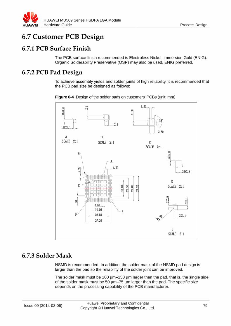
HUAWEI MU509 Series HSDPA LGA Module Hardware Guide Process Design
Issue 09 (2014-03-06) Huawei Proprietary and Confidential Copyright © Huawei Technologies Co., Ltd. 79
6.7 Customer PCB Design 6.7.1 PCB Surface Finish
The PCB surface finish recommended is Electroless Nickel, immersion Gold (ENIG). Organic Solderability Preservative (OSP) may also be used, ENIG preferred.
6.7.2 PCB Pad Design To achieve assembly yields and solder joints of high reliability, it is recommended that the PCB pad size be designed as follows:
Figure 6-4 Design of the solder pads on customers' PCBs (unit: mm)
6.7.3 Solder Mask NSMD is recommended. In addition, the solder mask of the NSMD pad design is larger than the pad so the reliability of the solder joint can be improved.
The solder mask must be 100 µm–150 µm larger than the pad, that is, the single side of the solder mask must be 50 µm–75 µm larger than the pad. The specific size depends on the processing capability of the PCB manufacturer.

HUAWEI MU509 Series HSDPA LGA Module Hardware Guide Process Design
Issue 09 (2014-03-06) Huawei Proprietary and Confidential Copyright © Huawei Technologies Co., Ltd. 80
6.7.4 Requirements on PCB Layout To reduce deformation, a thickness of at least 1.0 mm is recommended. Other devices must be located more than 3 mm (5 mm recommended) away from
the LGA module. The minimum distance between the LGA module and the PCB edge is 1.5 mm.
When the PCB layout is double sided, it is recommended that the LGA module be placed on the second side for assembly; so as to avoid module dropped from PCB or component(located in module) re-melding defects caused by uneven weight.
6.8 Assembly Processes 6.8.1 General Description of Assembly Processes
Tray modules are required at SMT lines, because LGA modules are placed on ESD pallets.
Reflow ovens with at least seven temperature zones are recommended. Use reflow ovens or rework stations for soldering, because LGA modules have
large solder pads and cannot be soldered manually.
6.8.2 Stencil Design It is recommended that the stencil for the LGA module be 0.15 mm in thickness. For the stencil design, see the following figure:

HUAWEI MU509 Series HSDPA LGA Module Hardware Guide Process Design
Issue 09 (2014-03-06) Huawei Proprietary and Confidential Copyright © Huawei Technologies Co., Ltd. 81
Figure 6-5 Recommended stencil design of LGA module
The stencil design has been qualified for HUAWEI mainboard assembly, customers can adjust the parameters by their motherboard design and process situation to assure LGA soldering quality and no defect.
6.8.3 Reflow Profile For the soldering temperature of the LGA module, see the following figure.
PCB PADS
Stencil design
Unit: mm
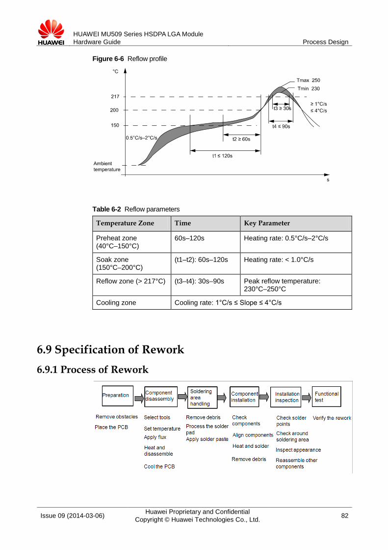
HUAWEI MU509 Series HSDPA LGA Module Hardware Guide Process Design
Issue 09 (2014-03-06) Huawei Proprietary and Confidential Copyright © Huawei Technologies Co., Ltd. 82
Figure 6-6 Reflow profile
Table 6-2 Reflow parameters
Temperature Zone Time Key Parameter
Preheat zone (40°C–150°C)
60s–120s Heating rate: 0.5°C/s–2°C/s
Soak zone (150°C–200°C)
(t1–t2): 60s–120s Heating rate: < 1.0°C/s
Reflow zone (> 217°C) (t3–t4): 30s–90s Peak reflow temperature: 230°C–250°C
Cooling zone Cooling rate: 1°C/s ≤ Slope ≤ 4°C/s
6.9 Specification of Rework 6.9.1 Process of Rework
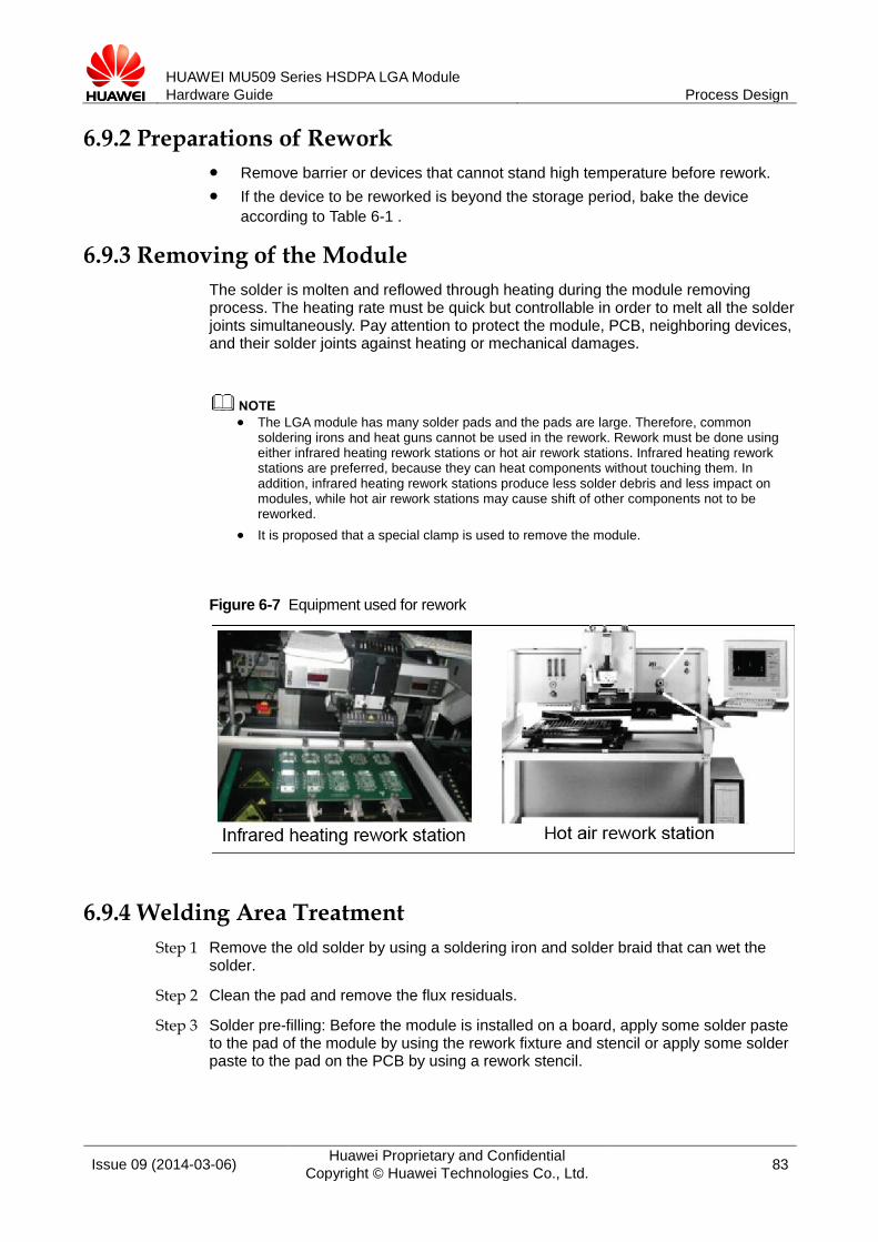
HUAWEI MU509 Series HSDPA LGA Module Hardware Guide Process Design
Issue 09 (2014-03-06) Huawei Proprietary and Confidential Copyright © Huawei Technologies Co., Ltd. 83
6.9.2 Preparations of Rework Remove barrier or devices that cannot stand high temperature before rework. If the device to be reworked is beyond the storage period, bake the device
according to Table 6-1 .
6.9.3 Removing of the Module The solder is molten and reflowed through heating during the module removing process. The heating rate must be quick but controllable in order to melt all the solder joints simultaneously. Pay attention to protect the module, PCB, neighboring devices, and their solder joints against heating or mechanical damages.
The LGA module has many solder pads and the pads are large. Therefore, common
soldering irons and heat guns cannot be used in the rework. Rework must be done using either infrared heating rework stations or hot air rework stations. Infrared heating rework stations are preferred, because they can heat components without touching them. In addition, infrared heating rework stations produce less solder debris and less impact on modules, while hot air rework stations may cause shift of other components not to be reworked.
It is proposed that a special clamp is used to remove the module.
Figure 6-7 Equipment used for rework
6.9.4 Welding Area Treatment Step 1 Remove the old solder by using a soldering iron and solder braid that can wet the
solder.
Step 2 Clean the pad and remove the flux residuals.
Step 3 Solder pre-filling: Before the module is installed on a board, apply some solder paste to the pad of the module by using the rework fixture and stencil or apply some solder paste to the pad on the PCB by using a rework stencil.

HUAWEI MU509 Series HSDPA LGA Module Hardware Guide Process Design
Issue 09 (2014-03-06) Huawei Proprietary and Confidential Copyright © Huawei Technologies Co., Ltd. 84
It is recommended that a fixture and a mini-stencil be made to apply the solder paste in the rework.
6.9.5 Module Installation Install the module precisely on the module and ensure the right installation direction of the module and the reliability of the electrical connection with the PCB. It is recommended that the module be preheated in order to ensure that the temperature of all parts to be soldered is uniform during the reflow process. The solder quickly reflows upon heating so the parts are soldered reliably. The solder joints undergo proper reflow duration at a preset temperature to form a favorable Intermetallic Compound (IMC).
It is recommended that a special clamp be used to pick the module when the module is
installed on the pad after applied with some solder. A special rework device must be used for the rework.
6.9.6 Specifications of Rework Temperature parameter of rework: for either the removing or welding of the module, the heating rate during the rework must be equal to or smaller than 3°C/s, and the peak temperature between 240°C–250°C. The following parameters are recommended during the rework.
Figure 6-8 Temperature graph of rework
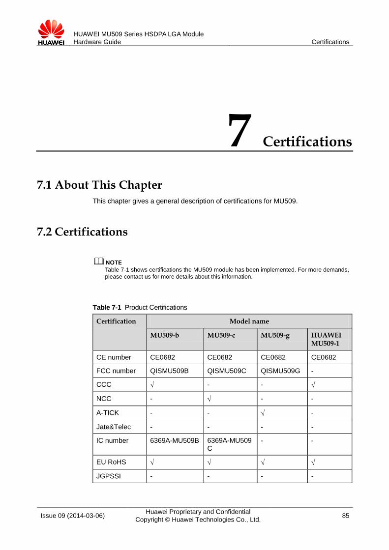
HUAWEI MU509 Series HSDPA LGA Module Hardware Guide Certifications
Issue 09 (2014-03-06) Huawei Proprietary and Confidential Copyright © Huawei Technologies Co., Ltd. 85
7 Certifications
7.1 About This Chapter This chapter gives a general description of certifications for MU509.
7.2 Certifications
Table 7-1 shows certifications the MU509 module has been implemented. For more demands, please contact us for more details about this information.
Table 7-1 Product Certifications
Certification Model name
MU509-b MU509-c MU509-g HUAWEI MU509-1
CE number CE0682 CE0682 CE0682 CE0682
FCC number QISMU509B QISMU509C QISMU509G -
CCC √ - - √
NCC - √ - -
A-TICK - - √ -
Jate&Telec - - - -
IC number 6369A-MU509B 6369A-MU509C
- -
EU RoHS √ √ √ √
JGPSSI - - - -
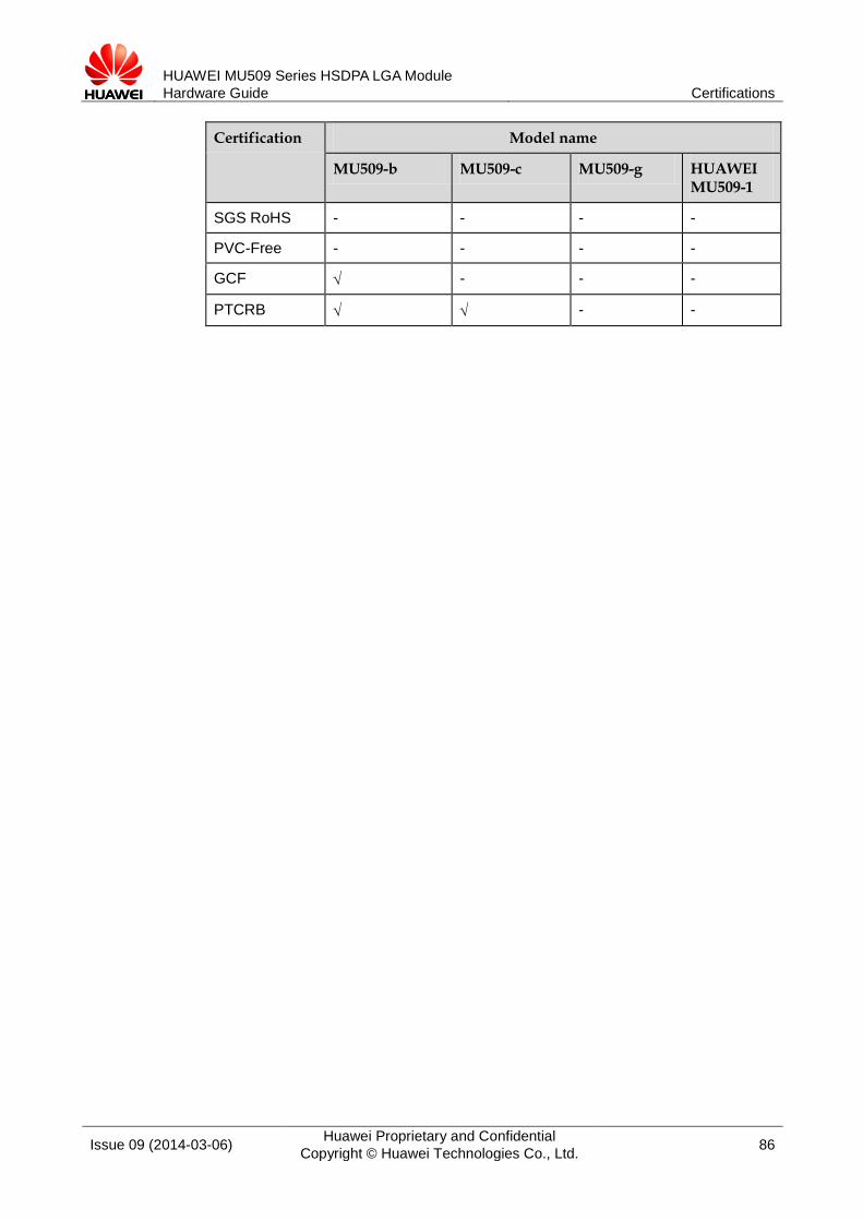
HUAWEI MU509 Series HSDPA LGA Module Hardware Guide Certifications
Issue 09 (2014-03-06) Huawei Proprietary and Confidential Copyright © Huawei Technologies Co., Ltd. 86
Certification Model name
MU509-b MU509-c MU509-g HUAWEI MU509-1
SGS RoHS - - - -
PVC-Free - - - -
GCF √ - - -
PTCRB √ √ - -

HUAWEI MU509 Series HSDPA LGA Module Hardware Guide Safety Information
Issue 09 (2014-03-06) Huawei Proprietary and Confidential Copyright © Huawei Technologies Co., Ltd. 87
8 Safety Information
Read the safety information carefully to ensure the correct and safe use of your wireless device. Applicable safety information must be observed.
8.1 Interference Power off your wireless device if using the device is prohibited. Do not use the wireless device when it causes danger or interference with electric devices.
8.2 Medical Device Power off your wireless device and follow the rules and regulations set forth by
the hospitals and health care facilities. Some wireless devices may affect the performance of the hearing aids. For any
such problems, consult your service provider. Pacemaker manufacturers recommend that a minimum distance of 15 cm be
maintained between the wireless device and a pacemaker to prevent potential interference with the pacemaker. If you are using an electronic medical device, consult the doctor or device manufacturer to confirm whether the radio wave affects the operation of this device.
8.3 Area with Inflammables and Explosives To prevent explosions and fires in areas that are stored with inflammable and explosive devices, power off your wireless device and observe the rules. Areas stored with inflammables and explosives include but are not limited to the following:
Gas station Fuel depot (such as the bunk below the deck of a ship) Container/Vehicle for storing or transporting fuels or chemical products Area where the air contains chemical substances and particles (such as granule,
dust, or metal powder) Area indicated with the "Explosives" sign
HUAWEI MU509 Series HSDPA LGA Module Hardware Guide Safety Information
Issue 09 (2014-03-06) Huawei Proprietary and Confidential Copyright © Huawei Technologies Co., Ltd. 88
Area indicated with the "Power off bi-direction wireless equipment" sign Area where you are generally suggested to stop the engine of a vehicle
8.4 Traffic Security Observe local laws and regulations while using the wireless device. To prevent
accidents, do not use your wireless device while driving. RF signals may affect electronic systems of motor vehicles. For more information,
consult the vehicle manufacturer. In a motor vehicle, do not place the wireless device over the air bag or in the air
bag deployment area. Otherwise, the wireless device may hurt you owing to the strong force when the air bag inflates.
8.5 Airline Security Observe the rules and regulations of airline companies. When boarding or approaching a plane, power off your wireless device. Otherwise, the radio signal of the wireless device may interfere with the plane control signals.
8.6 Safety of Children Do not allow children to use the wireless device without guidance. Small and sharp components of the wireless device may cause danger to children or cause suffocation if children swallow the components.
8.7 Environment Protection Observe the local regulations regarding the disposal of your packaging materials, used wireless device and accessories, and promote their recycling.
8.8 WEEE Approval The wireless device is in compliance with the essential requirements and other relevant provisions of the Waste Electrical and Electronic Equipment Directive 2012/19/EU (WEEE Directive).
8.9 RoHS Approval The wireless device is in compliance with the restriction of the use of certain hazardous substances in electrical and electronic equipment Directive 2011/65/EU (RoHS Directive).

HUAWEI MU509 Series HSDPA LGA Module Hardware Guide Safety Information
Issue 09 (2014-03-06) Huawei Proprietary and Confidential Copyright © Huawei Technologies Co., Ltd. 89
8.10 Laws and Regulations Observance Observe laws and regulations when using your wireless device. Respect the privacy and legal rights of the others.
8.11 Care and Maintenance It is normal that your wireless device gets hot when you use or charge it. Before you clean or maintain the wireless device, stop all applications and power off the wireless device.
Use your wireless device and accessories with care and in clean environment. Keep the wireless device from a fire or a lit cigarette.
Protect your wireless device and accessories from water and vapour and keep them dry.
Do not drop, throw or bend your wireless device. Clean your wireless device with a piece of damp and soft antistatic cloth. Do not
use any chemical agents (such as alcohol and benzene), chemical detergent, or powder to clean it.
Do not leave your wireless device and accessories in a place with a considerably low or high temperature.
Use only accessories of the wireless device approved by the manufacture. Contact the authorized service center for any abnormity of the wireless device or accessories.
Do not dismantle the wireless device or accessories. Otherwise, the wireless device and accessories are not covered by the warranty.
The device should be installed and operated with a minimum distance of 20 cm between the radiator and your body.
8.12 Emergency Call This wireless device functions through receiving and transmitting radio signals. Therefore, the connection cannot be guaranteed in all conditions. In an emergency, you should not rely solely on the wireless device for essential communications.
8.13 Regulatory Information The following approvals and notices apply in specific regions as noted.
8.13.1 CE Approval (European Union) The wireless device is approved to be used in the member states of the EU. The wireless device is in compliance with the essential requirements and other relevant provisions of the Radio and Telecommunications Terminal Equipment Directive 1999/5/EC (R&TTE Directive).
HUAWEI MU509 Series HSDPA LGA Module Hardware Guide Safety Information
Issue 09 (2014-03-06) Huawei Proprietary and Confidential Copyright © Huawei Technologies Co., Ltd. 90
Federal Communications Commission Notice (United States): Before a wireless device model is available for sale to the public, it must be tested and certified to the FCC that it does not exceed the limit established by the government-adopted requirement for safe exposure.
8.13.2 FCC Statement This device complies with Part 15 of the FCC Rules. Operation is subject to the following two conditions: (1) this device may not cause harmful interference, and (2) this device must accept any interference received, including interference that may cause undesired operation.
Warning: Changes or modifications made to this equipment not expressly approved by HUAWEI may void the FCC authorization to operate this equipment.

HUAWEI MU509 Series HSDPA LGA Module Hardware Guide Appendix A Circuit of Typical Interface
Issue 09 (2014-03-06) Huawei Proprietary and Confidential Copyright © Huawei Technologies Co., Ltd. 91
9 Appendix A Circuit of Typical Interface
J102
1
2
3
4
5
6P6
P5
P4
P3
P2
P1
U101
LGA120H-3030A
145144143142141140139138137136135134133132131130129128127126125
12412312212111611411211010810659585756545352504948 GND1
GND2GND3GND4GND5GND6GND7GND8GND9GND10GND11GND12GND13GND14GND15GND16GND17GND18GND19GND20
GND21GND22GND23GND24GND25GND26GND27GND28GND29GND30GND31GND32GND33GND34GND35GND36GND37GND38GND39GND40GND41M
ISC
Inte
rface
of
MU509_MISC
C10
2
150U
+
C10
1
150U
21
21
21
+
C10
3
**150U
+
C12
733
pF
C12
610
0nF
C12
51u
F
C12
933
pF
C12
833
pF
RV
104
V RV
105
V
C130 33p
C13
30.
5pF
L103 1.2n
C131 33p
S102 3
42
1
S101 3
42
1
L102
**27
n
J103
2 3
1 R110 0
D101
61 3
4
25
U101
LGA120H-3030A
7111
3533
923132
1312
848685
1423
7678747779737580
9899
65646362
3488708990
6610968
6967
5
768
120119118117
8382
38394041
91101
2221201918
2726252423
363072874293
6160
9495
113109105555146454443292815
141617
9796
104102
1003747
10381
111115107 MAIN_ANT
NCNC
POWER_ON_OFFNCNCNCRESIN_N
NCNC
EAR_OUT_NEAR_OUT_P
NCNCPS_HOLD
RESERVEDRESERVEDRESERVEDRESERVEDGPIOGPIOGPIOGPIOGPIOGPIOGPIOGPIO
NCNC
NCNC
JTAG_RTCKJTAG_TCKJTAG_TDIJTAG_TDOJTAG_TMSJTAG_TRST_N
NCNCNCNCNC
NCNCNCNCNC
LED_MODELED_STATUS
MIC1_NMIC1_PMIC2_NMIC2_P
NCNC
NCNCNCNC
PCM_CLKPCM_DIN
PCM_DOUT
PCM_SYNC
NC NC
NC NC NC NC
SIM_CLKSIM_DATA
NCSIM_RESET
SIM_VCC
NC NC
NC NC
SPKR_OUT_NSPKR_OUT_P
UART_CTSUART_DCDUART_DSRUART_DTR
UART_RINGUART_RTS
UART_RXUART_TX
NC NC
NC NC
USB_DMUSB_DP
NC
VBAT VBAT
VCC_EXT1VCC_EXT2
NC
NCVCOIN
WAKEUP_INWAKEUP_OUT
MIS
C In
terfa
ce o
f
MU509_MISC
R10
920
K
C119
220p
F
C11
4
150U
+
C12
1
22u
C12
2
22u
C12
3
1uF
C12
4
100nF
L101 2.2u21R104
**10
K
U102HPA00615DRVR
53
6
4 7
2
1OUT
ILIM
GND2EN
IN
FAULTGND1
R105 30KR103 1MEG
C10
9
1uF
C10
8
100nF
C10
7
4.7u
R107 180K
J101
0
54
6
98
123
7S2
P3P2P1
M1M2
S1
P4P5
RV103
V
C105 **1.8p
C106 100nF
R10
875
K
RV101
V RV102
VC104 **1.8p
C11
8
2.2U
R102 0
C11
7
**150U
+
U103
RT8015AGQW
9
8
10
11
7
6 5
4
3
2
1SHDN/RT
GND1
LX1
LX2
PGNDPVDD1
PVDD2
GND2
COMP
VDD
FB
C12
0
22p
C11
6
**150U
+
R101 0
C11
5
150U
+
C11
3
150U
+
C11
2
150U
+
C11
1
150U
+
R106
47K
MAIN_ANT
MAIN_ANT
GNDGND
RESIN_N
RESIN_N
POWER_ON_OFF
POWER_ON_OFF USB_DP
USB_DP
USB_DM
USB_DM
USB_D+
5V_P
5V_P
SIM_RESET
SIM_RESET
SIM_VCC
SIM_VCC
SIM_CLK
SIM_CLK
SIM_DATA
SIM_DATA
USB_D-
USB_5V
USB_5V
VBAT
VBAT
RF-INTERFACEPOWER_ON_OFF and RESIN_N
USIM CARD
POWER SUPPLYLGA Interface
NOTE:"**"means that this compent is not welded,but need to reserve component solder pad.
These are impedance matching circuit, the specificcapacitance and inductance value needs to beadjusted, based on the characteristic impedance ofthe practical PCB.
21
21
21
21
21
21
21
HUAWEI MU509 Series HSDPA LGA Module Hardware Guide
Appendix B Acronyms and Abbreviations
Issue 09 (2014-03-06) Huawei Proprietary and Confidential Copyright © Huawei Technologies Co., Ltd. 92
10 Appendix B Acronyms and Abbreviations
Acronym or Abbreviation Expansion
3GPP Third Generation Partnership Project
8PSK 8 Phase Shift Keying
AP Application Process
BER Bit Error Rate
BLER Block Error Rate
BIOS Basic Input Output System
CCC China Compulsory Certification
CE European Conformity
CMOS Complementary Metal Oxide Semiconductor
CS Coding Scheme
DC Direct Current
DCE Data Circuit-terminating Equipment
DMA Direct Memory Access
DTE Data Terminal Equipment
EDGE Enhanced Data Rate for GSM Evolation
EIA Electronic Industries Association
EMC Electromagnetic Compatibility
ESD Electrostatic Discharge
EU European Union
FCC Federal Communications Commission

HUAWEI MU509 Series HSDPA LGA Module Hardware Guide
Appendix B Acronyms and Abbreviations
Issue 09 (2014-03-06) Huawei Proprietary and Confidential Copyright © Huawei Technologies Co., Ltd. 93
Acronym or Abbreviation Expansion
GMSK Gaussian MinimumSshift Keying
GPIO General-purpose I/O
GPRS General Packet Radio Service
ISO International Standards Organization
LDO Low-Dropout
LED Light-Emitting Diode
LGA Land Grid Array
MCP Multi-chip Package
MDM Mobile Data Modem
MO Mobile Originated
MT Mobile Terminated
NC Not Connected
NSMD Non-solder Mask Defined
PA Power Amplifier
PBCCH Packet Broadcast Control Channel
PCB Printed Circuit Board
PDU Protocol Data Unit
PID Product IDentity
RF Radio Frequency
RoHS Restriction of the Use of Certain Hazardous Substances
RTC Real-time Clock
RFU For future use
SIM Subscriber Identity Module
SMS Short Message Service
TIS Total Isotropic Sensitivity
TRP Total Radiated Power
TVS Transient Voltage Suppressor
UART Universal Asynchronous Receiver-Transmitter
UL Up Link
UMTS Universal Mobile Telecommunications System
HUAWEI MU509 Series HSDPA LGA Module Hardware Guide
Appendix B Acronyms and Abbreviations
Issue 09 (2014-03-06) Huawei Proprietary and Confidential Copyright © Huawei Technologies Co., Ltd. 94
Acronym or Abbreviation Expansion
USB Universal Serial Bus
USIM Universal Subscriber Identity Module
VSWR Voltage Standing Wave Ratio
WEEE Waste Electrical and Electronic Equipment
WCDMA Wideband CODE Division Multiple Access