
Handwritten Digit Classification on FPGA
38
Handwritten Digit Classification on FPGA 18-545: Advanced Digital Design Kais Kudrolli, Sohil Shah, DongJoon Park Fall 2015
Transcript of Handwritten Digit Classification on FPGA

Handwritten Digit Classification on FPGA
18-545: Advanced Digital Design
Kais Kudrolli, Sohil Shah, DongJoon Park
Fall 2015

Table of Contents 1 Introduction ................................................................................................................. 5
1.1 Goal ........................................................................................................................ 5 1.2 Motivation .............................................................................................................. 5 1.3 Result ..................................................................................................................... 5
2 System Overview ........................................................................................................ 7 2.1 System Block Diagram ......................................................................................... 7 2.2 Approach ............................................................................................................... 8 2.3 Design Partitioning ............................................................................................... 8
3 Full Design Specification ............................................................................................ 9 3.1 Neural Network Background ................................................................................ 9 3.2 Simulation Stack ................................................................................................. 11 3.3 Software Stack .................................................................................................... 12 3.4 Hardware-Software Interface ............................................................................. 13 3.5 UART Stack ......................................................................................................... 14 3.6 Control Unit ......................................................................................................... 16 3.6 Tile ........................................................................................................................ 17
3.6.1 Forward Propagation Unit ............................................................................... 17 3.6.2 Sigmoid Function (PLAN Approximation) ....................................................... 18 3.6.3 Backpropagation Unit ..................................................................................... 19
3.7 Weight File ........................................................................................................... 20 3.7 Classifier .............................................................................................................. 21 3.8 Write FSM ............................................................................................................ 21
3.8.1 Camera Feed and Prediction .......................................................................... 21 3.8.2 Typeset Images .............................................................................................. 21 3.8.3 Bar Graphs ..................................................................................................... 22
3.9 Video Stack .......................................................................................................... 22 3.9.1 Video Encoder ................................................................................................ 22 3.9.2 Frame Buffer ................................................................................................... 22 3.9.3 HDMI Chip ...................................................................................................... 22
4 Testing Methodology ................................................................................................ 24 4.1 Simulators ........................................................................................................... 24 4.2 ILA ........................................................................................................................ 24
5 Status and Future Work ............................................................................................ 25
6 Schedule and Management Decisions .................................................................... 26 6.1 Tool Chain ........................................................................................................... 26

6.1.1 FPGA Board ................................................................................................... 26 6.1.2 Xilinx Tools ..................................................................................................... 26 6.1.3 Simulators ....................................................................................................... 26 6.1.4 Version Control ............................................................................................... 26
6.2 Schedule .............................................................................................................. 27 6.2.1 Initial Plan ....................................................................................................... 27 6.2.2 How the Semester Ended ............................................................................... 28
6.3 Team Workflow ................................................................................................... 28 6.4 Work Partitioning ................................................................................................ 29
7 Learnings and Future Wisdom ................................................................................. 30 7.1 Good Decisions ................................................................................................... 30 7.2 Bad Decisions ..................................................................................................... 30 7.3 What We Wish We Had Known .......................................................................... 31
8 Individual Pages ........................................................................................................ 32 8.1 DJ ......................................................................................................................... 32
8.1.1 What I Did ....................................................................................................... 32 8.1.2 Class Impressions .......................................................................................... 33
8.2 Kais ...................................................................................................................... 34 8.2.1 What I Did ....................................................................................................... 34 8.2.2 Class Impressions .......................................................................................... 34
8.3 Sohil ..................................................................................................................... 36 8.3.1 What I Did ....................................................................................................... 36 8.3.2 Class Impressions .......................................................................................... 37
9 References ................................................................................................................. 38

Forward We Kais Kudrolli, Sohil Shah, and DongJoon Park give the 18-545 staff permission to freely use this report and our code in anyway they see fit. Our GitHub repository is located at this URL: https://github.com/kkudrolli/Team-SDK-545

1 Introduction
1.1 Goal For our capstone design project, we wanted to build a computer vision system on an FPGA that would be able to recognize the digits 0 through 9 written by hand. We set out to accomplish this by implementing an RTL artificial neural network that could both make predictions and be trained in hardware. The hardware network would be supplemented by a software stack that would manipulate images of digits into a form recognizable to the network.
1.2 Motivation Computer vision is usually a software task that sometimes involves hardware
acceleration via GPUs. Thus, our intention was to (a) implement a typically software task in hardware and (b) accelerate neural network prediction using the inherent parallelism of hardware.
Our design was initially inspired by the work of Yann LeCun and Clement Farabet from NYU with deep learning using convolutional neural networks. However, the neural network architecture proposed in [1] was too complicated for a semester-long project and certainly more complicated than necessary to classify handwritten digits. Large convolutional networks such as the aforementioned one are more suitable when the inputs are huge and there are many possible classifications. Our network only requires 784 (28x28) input pixels and ten output classifications (one for each of ten images). For this reason, we based our neural network design on the neural network described in [5] by Nielson. This was a simpler, multi-layer, non-convolutional network, which was feasible to build in a semester and well-suited for classifying handwritten digits.
1.3 Result Ultimately, our handwritten digit classifier was able to predict the digits 0 through 9 when written in a variety of different handwriting styles and with varying degrees of sloppiness. We can also train the network both in software and dynamically in hardware. The network was not perfect and did struggle with certain images; however, in RTL simulation it approached the benchmarks for a two-layer network specified on the MNIST website. The benchmark on MNIST for a two-layer neural network with 300 hidden units is 95.3% accuracy [9], and we achieved 94.8% accuracy with two layers

and 128 hidden neurons. Moreover, when the network predicted a number incorrectly in hardware, it showed low confidence values and was generally close to the correct prediction. The accuracy of the network largely depended on the amount it was trained, but lighting and positioning of the camera also sometimes affected it.
2 System Overview
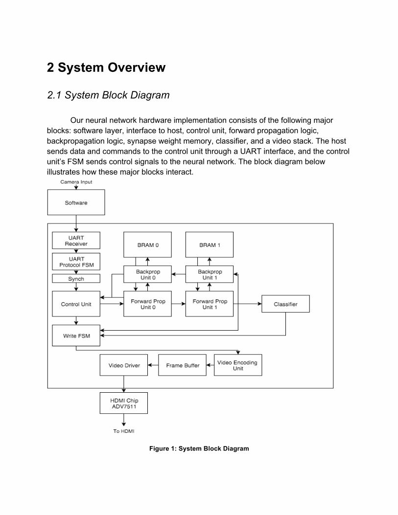
2.1 System Block Diagram
Our neural network hardware implementation consists of the following major blocks: software layer, interface to host, control unit, forward propagation logic, backpropagation logic, synapse weight memory, classifier, and a video stack. The host sends data and commands to the control unit through a UART interface, and the control unit’s FSM sends control signals to the neural network. The block diagram below illustrates how these major blocks interact.
Figure 1: System Block Diagram

The control unit sends data and commands to the first forward propagation unit. This unit computes the output for the first layer of neurons. That output is propagated to the next unit in the sequence and so on until the classifier. The classifier predicts which handwritten digit has been sent and then sends this information to the video stack. The video stack takes the classification, builds a stylized image of the digit, and writes this data to the frame buffer. Finally, the video driver draws the frame buffer’s contents to the screen. When in training mode, the output of the neural network is also sent backwards through the backpropagation units, and the BRAM holding the weights is updated.
2.2 Approach Our approach consisted of the following workflow. First, we modularly tested our
own parts and integrated them. For the purpose of testing, we had C simulator that behaved the same as our Verilog design. After making sure our C simulator was working, we tested on Verilator, a fast Verilog simulator. Finally, when the system did not work as expected, we used ILA to monitor internal signals of the system. By having multiple layers of testing, we were able to effectively debug the integrated design.
2.3 Design Partitioning In general, we tried to divide the design into the software, software-hardware interface, neural network, and display. Thus, we tried to break down the design into portions that were both similar in functionality and equally time-consuming to implement. We felt that our system was inherently modular, so breaking it down as described above felt natural. These groups also naturally broke down into subgroups. For example, a neural network typically consists of a forward propagation and backpropagation; therefore, we broke up the NN into forward propagation units, backpropagation units, and weight files. Overall, we felt that this partitioning scheme worked well for us because it was mostly successful in breaking down the work into equal chunks. In cases when it was not, one person was just given multiple chunks to even out the workload. For instance, Kais initially was working on software, but this was not as much work as the neural network. Consequently, he also worked on the software-hardware interface, and the work was balanced.

3 Full Design Specification
3.1 Neural Network Background A neural network is composed of the following features: ● An input layer that takes in data from some external source ● A set of hidden layers which transform this data in some way and contain:
○ Summing nodes to add up contributions from previous layer’s neurons, ○ Some type of activation function that defines the response of each neuron,
and ○ Weights for each contribution to the next layer
● An output layer to output the network’s calculation to some external target A diagram of a network is shown below:
Figure 2: Neural Network [6]
The input layer in our case contains a 32-bit integer for each pixel in the input
image. The hidden layer consists of 128 neurons, and the output layer contains 10 32-bit integer outputs. The number 128 was experimentally determined using a C simulator of a neural network. Each output is the activation of that particular digit. In our case, the nonlinear activation is an approximation of the sigmoid function. We can perform a single feed-forward propagation as follows:

● For each input of the input layer and neuron of the first hidden layer, multiply the input by the weight for that input and neuron
● For each neuron in the hidden layer, sum the weighted contributions from all inputs
● For each neuron, evaluate the activation of the summed contribution by passing the sum into an activation function (such as the sigmoid)
● Repeat with the next layer, this time using the outputs of the previous layer as inputs to weight for the next layer
● Output the last layer’s activations as a prediction vector ● Use this vector and a classifier (such as a softmax function) to create a
classification
The actual training of the network works by passing a large number (>100,000) of images as inputs to the network and updating the weight matrices backwards by backpropagation using gradient descent.
Figure 3: Backpropagation [3]
In this method, we have a target we wish to reach, and we calculate the
difference from the target. This difference is then weighted by the gradient of the activation and applied backwards through each layer. It can be summarized as follows: ● Perform a feed-forward propagation ● Calculate the error of the forward-propagated result relative to a target vector ● Scale this error by the gradient of the activation for this neuron layer ● Multiply the update vector by the learning rate ● Apply this weight difference to the current weights to update this layer’s weights

● Move on to next layer by propagating this error to update all weights in the network
If the learning rate is tuned correctly (as we did experimentally), then this
algorithm will converge to a certain accuracy. This usually occurs after a very large number of backpropagations with a training set of enough distinct samples.
3.2 Simulation Stack A very important piece that made this project succeed was the “simulation stack,” as we call it. Once we understood the math behind the network, we built from scratch a C-level model of the network on which we based all of our RTL design decisions. Then, we used Verilator to build a C++ model of the network to debug and make design decisions for the final project. Finally, Vivado Sim and VCS comprised the last layer of simulation and were closest to the hardware.
Figure 4: Simulation Stack The C simulator had a variety of modifiable parameters such as number of
training images, number of training iterations, learning rate, target vector bias, initial

weight distribution, and many others. This and the fact that we built a file format to store a pre-made network allowed for very quick debugging and changes to our network structure.
3.3 Software Stack As shown in Figure 5, the software portion of our design is divided into two components: reading from the MNIST database and image capture capture/manipulation. The software runs on a host machine with a webcam and serial interface to the FPGA.
Figure 5: Software Diagram
MNIST is a database compiled by Yann LeCun containing thousands of handwriting samples of the digits 0 through 9. We use this database both to train and test our neural network. The MNIST training set has 60,000, and the test set has 10,000 images [9]. They are stored in a special file format called idx, which has a short header followed by all the 28x28 8-bit pixel images stored in one file. Thus, our host machine code runs a C program to parse the images into separate byte arrays. We chose to use MNIST to train our neural network because it is readily available, easy to use, and a common training set for digit classification. Since MNIST is mainly used for training, we implemented host software to take images of real handwriting samples and demonstrate the capability of the neural network. The front-end interface, written in Python using the OpenCV library, allows a user to continuously capture images of digits from the host machine’s webcam. The webcam images must be manipulated so that they are in the same form as the MNIST

images: 28x28 pixels, black/white/gray, and 8-bits per pixel. OpenCV’s Python API functions that make it simple to perform this manipulation. Therefore, we use it to first grayscale and threshold the image. We use inverse thresholding with a threshold of 65, meaning that any byte with a value less than or equal to 65 would be made white, and any byte greater than 65 would be made black (as shown in Figure 6). Then, we normalize the image to try to account for images taken in different lighting by forcing all RGB values to be in a certain range. Finally, we downsize the image to 28x28 pixels. The manipulated image is stored to disk. At this point, the image is black and white and 28x28, but to be like MNIST each pixel must be encoded by 8 bits not 32. Since the image was grayscaled, all the R, G, and B values for a given pixel are the same. Therefore, we run C code to take a webcam image on disk and store just the R values in a byte array of length 784, same as the MNIST images.
Figure 6: Inverse Thresholding To avoid having a software layer, we could have fed the camera input directly
into the FPGA and done image manipulation in hardware. However, we decided it was more practical to use OpenCV’s simple, optimized API for image manipulation. This prevented us from having to write our own grayscale, normalization, downsize, and threshold modules in hardware and from having to interface with the camera from the board. These modules would have added significant complexity and also would have taken precious time we really needed to devote to the neural network. Also, with OpenCV the webcam we used worked out of the box through USB, preventing us from having to do any complex interfacing. Moreover, we would have had to upload the MNIST database into BRAM and access it from hardware. Accessing the MNIST database from C on the host machine was simpler and gave us more control over training and testing. In software, it was easy to choose which images to send whereas this would have been harder on the FPGA.
3.4 Hardware-Software Interface To interface with the FPGA, our host computer is connected to it via UART. The physical connecting cable is a USB cable. On the FPGA, the cable plugs into a

Silicon Labs CP2103 USB-to-UART bridge chip. Therefore, the interface on the FPGA side consists of an RX and TX pin rather than USB pins. On the software side, the CP2103 comes with Virtual COM port drivers. These contain USB drivers but also provide an interface that can be written/read like any other serial interface. Our host software has a C program that reads MNIST or webcam image byte arrays and writes them to the serial port. The baud rate of this serial port is limited to approximately 1 Mbps (exactly 921,600 bps) on the lab computers. This speed is suitable for sending our small images to the FPGA. The UART did become a bottleneck in our system which could have been resolved if we had supported a higher bandwidth transfer interface such as USB, Ethernet, or PCIe. However, all of these were significantly more difficult to implement than UART, and we felt it was important at the time for us implement a transfer quickly to leave as much of the semester for building our neural network.
3.5 UART Stack To properly handle the UART transfer, we implemented a UART stack to interpret a custom byte-level protocol. The stack was split into three parts: the receiver, the protocol FSM, and the synchronizer. The receiver interfaced with the signals from the USB-to-UART bridge chip. The interface consists of RX and TX lines for serial receive and transfer, respectively. There are also RTS (ready to send) and CTS (clear to send) lines for flow control. Since we did not transfer anything from the FPGA to the host machine, the RTS and TX lines were unused. The receiver asserted the CTS line whenever it was in a state where it could receive data. The RX line was most important as this had the actual data. The receiver sampled this line at the UART sampling clock frequency of 14 MHz divided by the baud rate of approximately 1 Mbps. It looked for an 8-bit UART transfer like the one shown in Figure 7 and reconstructed each byte using a shift register.
Figure 7: UART transfer of one byte [8] The protocol FSM receives bytes from the receiver one at a time and interprets them based on a simple, custom protocol we designed on top of UART depicted in

Figure 8. The protocol looks for a START byte, which is made unique by the software side of the transfer (anytime a byte with the START byte value is seen on the software side, the value - 1 is sent instead). Then, the FSM looks for a TRAIN or TEST byte, which denotes whether the following image is a training or a testing sample. Next, the FSM buffers the LABEL, which is the digit to which a training image corresponds. Lastly, the FSM buffers the next 784 bytes in a shift register to reconstruct the image and asserts a start signal when 784 bytes have been seen.
Figure 8: Custom UART byte-level protocol The synchronizer synchronizes the transfer of the image, label, and start signal from the UART sampling clock domain to the neural network’s clock domain. It is implemented using a register that is clocked on uart_sampling_clk, which outputs to a second register clocked on the system clock. The synchronizer was originally used in the system because these two clocks were different; however, we later decided it was be easier to simply make the clocks the same and avoid synchronization issues. We decided this because our bottleneck was UART, and we were getting timing failure in the neural network with a 50 MHz system clock. Thus, we simply slowed down the clock to 14 MHz to avoid timing failures and synchronization in one step.

3.6 Control Unit
Figure 9: Control Unit
This FSM consists of four states (as shown in Figure 9):
1. idle ○ The FSM simply waits for a start signal to indicate the image and label are
ready ○ Start and train are buffered on a start ○ Moves to forward propagation and asserts do_fp on a start
2. fwd_prop ○ This state is for performing a forward propagation: it commands the tiles to
take a weighted sum of inputs to output the activation of a set of neurons ○ Once forward propagation is complete, the network asserts fp_done, and
the FSM either commands the network to train on this image via backpropagation or just display the prediction

3. back_prop ○ This state commands the backprop units to determine error and propagate
this error backwards through the system ○ Once all errors are found, the weight file is updated with a weight delta
and the network asserts bp_done 4. display
○ This state is reached after an fp_done and train is not asserted ○ It commands the write FSM to draw an updated prediction
3.6 Tile
3.6.1 Forward Propagation Unit The tiles are forward propagation units that calculate a vector of neural outputs based on given weights and inputs. The tiles contain some number of neurons (in our case, 128 seems to work well), and each neuron has an associated activation function. This activation function is the sigmoid function:
The tile takes in a vector of weights for each neuron and weights all outputs of
the previous layer by this vector. The resulting vector is summed to give a net neural input. This input is then passed through the sigmoid function. The output of the sigmoid is the activation of the particular neuron. This is performed for all neurons in the tile and output as a vector for the next layer to use.
Figure 10: Tile

Figure 11: Neuron
3.6.2 Sigmoid Function (PLAN Approximation) We found an efficient piecewise linear approximation of a nonlinear function (PLAN) for the activation function [2]. This technique gives a close approximation to the sigmoid function as shown below. Alternative was a look up table, but considering the large silicon area it takes and the latency to access the block RAM, we use PLAN instead. As shown in the table, there are four sections with different linear equations when x is positive, and when x is negative, the value is simply Y = 1-Y.
Figure 12: Sigmoidal approximation using piecewise linear technique [2]

Table 1: Implementation of PLAN [2]
Our sigmoid, even though it does use this approximation, was still not fast
enough to synthesize. Therefore, we had to pipeline it into two stages and calculate the multiplication and the addition in two separate steps.
3.6.3 Backpropagation Unit Our goal for the network is to find weights that minimize a function called the cost function, which is defined as below:
𝐶 = !!
! 𝑦 𝑥 − 𝑎! 𝑥 !when y(x) is a desired output, a is the actual
output, and L refers the output layer L.
We won’t go over full details of mathematical equations and proofs for them, but the idea, a technique called gradient descent, is that we keep decreasing the cost function C until it reaches the global minimum.
Another quantity, error, 𝛿, is defined as below:
when 𝑧!! is the weighted input for neuron j in layer l. Error in the output layer L can be evaluated with the equation below.
when 𝜎′is the derivative of our activation function. 𝛿!indicates how fast the cost function changes as a function of activation output in the output layer L. Also note that given the cost function in a quadratic form as above,
when a is the actual output and y is the desired output.

Small 𝛿! means we are close to optimal. Weight values should be adjusted in a way that they minimize 𝛿!. Once 𝛿! is evaluated, 𝛿!, . . . , 𝛿!!! can be calculated with the equation below:
.
Finally, using 𝛥𝑤 = 𝛿𝑙𝑦𝑙−1𝑇 , we update weight values in weight file hoping that error in the output layer L, 𝛿!, becomes small which leads to the conclusion that actual output and ideal value are similar. A simplified diagram of this is shown below:
Figure 12: Backpropagation Unit
3.7 Weight File Each neuron in layer has a quantity “weight” corresponding to the arbitrary
neuron in the next layer l+1. So, when we have m neurons in layer l and n number of neurons in layer l+1, there are total m×n weights from neurons in layer l to neurons in layer l+1. In our implementation, we first had 128 BRAMs for 1st layer to enable parallel access, but after realizing it can be done with one BRAM, we ended up using 4096 x 784 BRAM for 1st layer and 320 x 128 for 2nd layer. Thus, it takes 784 cycles to extract
all the weight values for 1st layer and 128 cycles for 2nd layer. When Δw is calculated from backpropagation, the update signal should update all the weights in a certain layer. Similarly, it takes 784 cycles to update all the weight values for 1st layer and 128 cycles for 2nd layer.
3.7 Classifier We originally planned to implement softmax function for the classifier but ended
up simply showing the activations for our ten output neurons in bar graph form. Still, it represents the confidence of our prediction, and the digit whose value is the maximum is our final classification result.
3.8 Write FSM The write FSM’s main purpose is to draw the webcam feed and the typeset image of the prediction onto the HDMI monitor. It also draws the bar graphs to show the confidence estimate for each digit. While it does not accomplish this directly, it writes the appropriate bytes to the video encoder to achieve this display. The combinational logic blocks to generate the typeset image are a separate module as is the FSM to generate the bar graphs.
3.8.1 Camera Feed and Prediction The main portion of the write FSM sets the write address and write data of the video encoder on every cycle. On a start signal, the image from the UART stack is buffered, and every cycle afterwards the address and data are updated to draw the camera feed onto the screen. The FSM takes every byte of the image and writes it to a 10x10 pixel area on the screen. Thus, the full 28x28 image is blown up to 280x280 pixels. The same thing is done for a prediction image, except the write process begins on an fp_done signal from the neural network, and the image data comes from the typeset image module described below.
3.8.2 Typeset Images The typeset image combinational logic block is effectively a large decoder that outputs a 784*8-bit image vector based on the prediction (maximum result of the neural network activations). The ten possible image vectors are hard-coded into the logic fabric, and the vectors are generated prior to synthesis using a Python script we wrote to convert typeset images of digits into SystemVerilog hexadecimal constants.

3.8.3 Bar Graphs The bar graph FSM waits for a start_graph signal asserted by the write FSM when both the prediction and webcam feed have been drawn. The start_graph signal is also the select line of a mux that muxes the address/data from the write FSM and the bar graph FSM. Thus, the bar graph FSM also drives the address and data to the video encoder. It draws ten bars, one for each digit. The height and color of each bar is a function of how high the activation of the corresponding digit is: higher activation means a darker, taller bar and lower activation means a lighter, smaller one.
3.9 Video Stack
3.9.1 Video Encoder The video encoder decides which pixels to write to the frame buffer. It consists of parts for the camera image input, typeset image prediction, and bar graphs. The camera image input and the typeset image prediction were both handled by the write FSM described above. This FSM looped through bytes of an image buffer and wrote them in 10x10 pixel blocks to the screen to scale the 28x28 image up to 280x280. The FSM drew whichever image was available first, then switched to draw the other one if it was queued. The bar graphs were drawn as pixel lines if the output of the network went above a certain threshold. All data was drawn into frame buffer for display over HDMI.
3.9.2 Frame Buffer The frame buffer design is a simple, dual-ported BRAM that contains 24 bits for each pixel. The frame buffer is written to by the video encoder and can be read at the same time (and at a different clock) by the HDMI output FSM. The framebuffer is initialized with our background image and then updated using bar graph and image data.
3.9.3 HDMI Chip Writing to the HDMI Chip is done with a simple FSM that loops through all of the frame buffer, incrementing the frame buffer address when data enable on the HDMI encoding is asserted. The HDMI signals themselves are generated much like VGA signals are: there are HSYNC, VSYNC, and DE lines driven by a set of counters and comparators. Programming the HDMI chip itself took slightly more work. First, an I2C master protocol FSM was created. This protocol FSM can perform I2C read and write transactions as defined by the waveform below:

Figure 13: I2C Bus Protocol [4]
In the above example, to write a register, first we send address as the device
(HDMI chip) address, then the first data byte is the register offset, then second data byte is data to write to register.
To program the HDMI chip (ADV7511), the following sequence of register write operations were performed:
Device Address Data1 (register offset)
Data2 (data to write) Operation Description
8’b11101000(0xE8) 8’b00100000(0x20) N/A Write to bridge device on VC707 board (address 0xE8) to enable configuration of HDMI chip over I2C
8’b01110010(0x72) 8’b01000001(0x41) 8’b00010000(0x10) Power up transmitter
8’b01110010(0x72) 8’b10011000(0x98) 8’b00000011(0x03) Fixed reg - must be set
8’b01110010(0x72) 8’b10011010(0x9A) 8’b11100000(0x70) Fixed reg - must be set
8’b01110010(0x72) 8’b10011100(0x9C) 8’b00110000(0x30) Fixed reg - must be set
8’b01110010(0x72) 8’b10011101(0x9D) 8’b00000001(0x01) Fixed reg - must be set
8’b01110010(0x72) 8’b10100010(0xA2) 8’b10100100(0xA4) Fixed reg - must be set
8’b01110010(0x72) 8’b10100011(0xA3) 8’b10100100(0xA4) Fixed reg - must be set
8’b01110010(0x72) 8’b11100000(0xE0) 8’b11010000(0xD0) Fixed reg - must be set
8’b01110010(0x72) 8’b11111001(0xF9) 8’b00000000(0x00) Fixed reg - must be set
8’b01110010(0x72) 8’b00010110(0x16) 8’b00110000(0x30) Setup video output mode

4 Testing Methodology
4.1 Simulators The simulators were crucial to the project’s success and the only reason we got anything to work at all. Had we begun writing the network directly in Verilog we would have not got much done in the end. The simulation drove our debugging efforts because whenever something did not work, we could step cycle by cycle in our C simulator to see where values differed.
One incredibly useful technique was using the waveform viewer in Vivado Sim and comparing values of intermediate vectors with those in Verilator and C simulators to see exactly at which time step there was a difference. This would be completely impossible to debug with just hardware alone or without the higher-level simulators.
4.2 ILA Integrated Logic Analyzer (ILA) IP core enabled us to monitor the internal signals
of a design. It is incredibly useful debugging feature in Vivado. We actively used ILA when we had random classification results for forward propagation in order to narrow down from where the randomness was coming.

5 Status and Future Work Our system perfectly classifies handwritten digits from 0 to 9 under well-designed
environment; we need bright light so that there is no noise in the webcam image capture, and a person should draw the number reasonably large and thick. It would have been better if we could create noise tolerant image I/O system or just simply have a lamp right next to webcam. Also, we could get our system to work even if a person writes digits relatively small or thin.
Since now the network is working with digits, we can expand the classifier to letters. To do this, we may need to change the size of neural network with the aid of our simulator. We could also expand our system to split images of multiple digits or letters to detect numbers and words.

6 Schedule and Management Decisions
6.1 Tool Chain
6.1.1 FPGA Board We chose the VC707 (Virtex 7) as our FPGA board because we anticipated that our neural network design would require a large amount of LUTs and DSP blocks. Ultimately, this choice was correct because we our final synthesized design used approximately 50% of the LUTs and 80% of the DSPs. The board also suited our needs well because Sohil had an existing implementation of an HDMI controller for the chip on our board. Furthermore, the UART-to-USB bridge chip on our board came with convenient software drivers that made a UART transfer manageable.
6.1.2 Xilinx Tools We used Vivado Design Suite (as everyone was required to do this semester) for our FPGA synthesis and programming. Vivado does have certain advantages, namely that it can support the Virtex 7 board, Vivado Sim is a useful pre- and post-synthesis simulator, and ILA is a life-saver when debugging the design once it has been programmed. However, its robustness is questionable. We witnessed it crash a number of times at random and once when we simply unplugged the programming cable (which was not even in use).
6.1.3 Simulators Our group used VCS to perform module-level testing and verify basic functionality with simple SystemVerilog testbenches. For integration testing, we used a tool called Verilator, a free Verilog HDL simulator [7]. This was very useful both for testing the neural network on its own and for testing integration between the software side of system with our hardware. Verilator allows you to call your Verilog from C code, meaning we could combine our C transfer programs with our RTL code.
6.1.4 Version Control For version control, we used git and GitHub extensively. In general, our team was disciplined about committing and pushing changes. At the beginning of the semester, we agreed on a style for our commit messages that would be helpful to each other. Proper use of git sometimes gave us the flexibility of working remotely if we could not come into the lab. Requiring groups to use git and GitHub was definitely a good decision on the part of the professors.

6.2 Schedule
6.2.1 Initial Plan Initially, we planned out the first month of work and decided we would update the schedule based on our progress in the previous month. We roughly maintained this pattern and updated our schedule periodically. These checkpoints and our planned weekly tasks are detailed in the table below. Our second checkpoint came very quickly after the first one because we had to do our design review, and we had all been very busy and unable to make that much progress. For the most part, we tried to keep our schedule as aggressive as possible, knowing that even if we were not able to fully meet it we would likely still make good progress.
Week of Kais Sohil DJ All
9/14 Camera input and manipulation
HDMI Ethernet Finalize design, work on peripherals
9/21 C image I/O NN tiles Memory C simulator of NN, finish peripherals
9/28 Parse MNIST, finish image I/O
Backprop for simulator
PCIe Finish C simulator
10/5 CHECKPOINT Activation function
Start backprop Integrate forward prop
Work on simulator integration and test
10/12 Start design review
Create RTL Verilator simulation env
Experimentally determine best NN design using sim
Start basic RTL blocks, experiment with simulator to finalize design, backprop in sim on hold
10/19 CHECKPOINT
Control unit Verilator simulation env, tile
Weight file Finish design review
10/26 Integrate sw and UART stack
Integrate NN Integrate NN Integrate forward propagation components
11/2 Integrate sw, UART stack, and control unit
Backprop unit Weight update Work on individual backprop pieces and integrate fwd prop
11/9 Webcam live feed
Backprop unit Backprop unit Backprop unit and system integrated with the sw
11/16 Webcam feed and integration
Backprop unit Backprop unit Backprop unit and system integrated with the sw
11/23 Polish demo Polish demo Polish demo Polish the demo, start final presentation and write-up, BUFFER WEEK
11/30 Demo Demo Demo Demo, BUFFER WEEK
6.2.2 How the Semester Ended We were perhaps too optimistic about how long it would take us to get forward propagation integrated and working on the board. So, our planned schedule fell apart after the design review when we encountered some nasty integration bugs and other difficulties. Below, we have detailed how the last few weeks of the semester actually transpired. In the end, we only got forward propagation working a week before final presentations and spent the remaining two weeks trying to get backpropagation to work while polishing up our demo in parallel. Also, note the “-”s denote that everyone was mostly working on the same task.
10/19 CHECKPOINT
Control unit Verilator simulation env, tile
Weight file Finish design review
10/26 Integrate sw and UART stack
Integrate NN Integrate NN Integrate forward propagation components
11/2 Integrate sw, UART stack, and control unit
Backprop unit Weight update Work on individual backprop pieces and integrate fwd prop
11/9 - - - Debug fwd prop integration
11/16 - - - Debug fwd prop integration
11/23 - - - Debug fwd prop integration
11/30 Polish demo Backprop Polish demo Fwd prop and polish demo
12/7 - - - Backprop and polish demo
6.3 Team Workflow Most weeks, our team workflow was as follows. We had a meetings at the
beginning of the week to take stock of last week’s progress, set goals for the week, divide up tasks, and established when we would meet next to work together. We spent

50-75% of the week on individual components implemented in parallel and the last 25-50% on integration and testing. Kais kept account of the schedule on GitHub, the tasks in progress, and who was doing them.
This workflow continued until the end of the semester when almost all of our work was integration and debugging of the forward or backpropagation. During those few weeks, neither the tasks nor the partitioning of work changed. Thus, we almost always worked together on the same task with the rationale that multiple eyes would be able to catch bugs more quickly.
6.4 Work Partitioning In general, the work was partitioned as follows. Kais worked on the software and software-hardware interface. DJ and Sohil worked on the neural network, where DJ focused more on the weight file and Sohil focused more on the computation. The display work was shared by everyone: Sohil owned the HDMI video stack because it was his code from a previous project while DJ and Kais both worked on the write FSM.

7 Learnings and Future Wisdom
7.1 Good Decisions ● Keeping a schedule the whole semester was a particularly good decision. It
served as a benchmark for progress and also incentivized us to work harder when we fell behind.
● Building and using a C simulator of the neural network was well worth our time. Even though implementing the simulator prevented us from getting to RTL until October, this was not time wasted. The simulator helped us become familiar with neural networks, and thus it made RTL easier. Furthermore, it was a useful reference implementation to compare against when we started implementing the RTL network. Lastly, it served its original purpose by helping us find an accurate design for our network.
● Learning how to use ILA was incredibly useful. It was the only way we could have understood what our bug was when we were getting random predictions from our neural network on the FPGA.
● Choosing a different type of project (rather than a game) was also a good decision. Working on something that had not been done in 18-545 before was interesting, and it was very fulfilling to get a different kind of FPGA project working.
7.2 Bad Decisions ● We thought we needed to devote all of our time to the neural network. As a
result, we shied away from getting our hands dirty with more complex transfer interfaces like PCIe and Ethernet. This came back to bite us because our bottleneck remained UART even at the end of the semester. We think that if we had tried to understand the AXI interface to some of the IP blocks Xilinx provides for PCIe and Ethernet interface, we could have had a faster transfer and higher resolution images.
● It is far easier to debug a single module than to debug the integrated part. If we had fully tested each module then integrated, we could have saved more time instead of all three of us spending couple hours finding out a small bug in some function.

7.3 What We Wish We Had Known First, we wish we had known just how long integration takes. We were naive to think we could integrate all of the forward propagation in a week. Integration issues hampered us for at least three weeks, meaning it took us 3x longer to integrate than to actually write the RTL. We also wish we had known beforehand how long synthesis runs could take. We were initially taken aback when our neural network started to take almost one hour and thirty minutes to perform synthesis, implementation, and create the bitstream. Had we known that this would be the case, we would have started parallelizing synthesis runs much earlier in the semester. Finally, we wish we had known that even though ILA adds time to your synthesis run, it is incredibly useful for debugging and well worth the wait. Initially, we hesitated to use ILA because we thought it would just take too long to be useful.

8 Individual Pages
8.1 DJ
8.1.1 What I Did I started by watching online lectures related neural network architecture and tried
to understand the math behind it since I wasn’t familiar with the concept. I might be one of few students who had previous experience in medium size projects using Vivado, so when we were doing lab1, 2 or our own projects, I helped my teammates to get familiar with Vivado.
We originally wanted to transfer webcam-captured data to FPGA using Ethernet. However, I struggled to get AXI EthernetLite working and changed to PCIE because F11 Sidekicks and F13 Astro Team used PCIE. I contacted Gun Charnmanee, a friend of mine, who was on F13 Astro Team and got access to their Git repository. We realized that we didn’t have a PCIE ribbon cable in lab and while waiting it to be delivered we searched for alternatives. Luckily, we found that UART is relatively simple compared to options we had had so far although the speed is slower than other options. We thought the maximum speed of UART would be enough for our project and decided to stick to it. We started off creating simulator in C, and my part was weights.c which contains initWeight, freeWeight, updateWeight, etc. Sohil who was in charge of tile and I had miscommunication on how we define the number of layers and accessing the weight file, but we managed to get over it. With Kais, I also worked on creating piece-wise sigmoid function that would replace our original linear sigmoid function for better accuracy.
I modified Sohil’s HDMI code so that now it has two squares on the screen whose size is now enlarged to 280 x 280. Once we were sure that C simulator is working, we started implementing RTL. I needed to implement two versions of weight file, one with 3-D array version for Verilator purpose and one with Vivado IP for actual design. For the latter, I wasn’t sure how many BRAMs I would use, because if I use only one BRAM (1st layer: 32 x 784 x 128) for one neuron (1st layer: 784 neurons, 2nd layer: 128 neurons, 3rd layer: 10 neurons), it would take 784 x 128 cycles to extract all the weight values for 1st layer. We decided to use 128 BRAMs for the first layer so that it would take only 784 cycles to get all the weight values (1st layer: 32 x 784). I created tcl file to ease this job. I also implemented sigmoid function in hardware.
With this many BRAMs, it took so long for synthesis (3 hours). Also, there were some random error messages that I had never seen before. The weirder thing was that I copied the entire project to Vivado installed in my laptop, version of 2015.1, and the error message was gone. (the error occurred with 2015.2 version) We were kind of stuck at this point, and I wanted to make synthesis quicker. Then, I realized that what

TA said on Piazza totally makes sense, and rather than having 32x784 for each BRAM, I decided to have 4096x784 so that 128 neurons’ weight values are concatenated. We still struggled getting forward propagation working. I found some minor mistakes resulted from the fact that addition “+” precedes shift “>>” in Verilog. The major issue was when we tried to synthesize the project, it kept raising “RAM issue” saying that it runs out of RAM. We could get this around when Sohil pipelined sigmoid function, but now the classification results were random even though there is no randomness in our system. (should be deterministic!) In my individual research, when the system clock frequency was too high, the system sometimes broke even though it didn’t raise any timing violations. So I suggested reducing clock frequency from 200MHz to 100MHz, and now the random behavior was gone. Getting our system deterministic was very optimistic for us, and we were able to easily find out that why it resulted in wrong, deterministic classification; we were accessing weight values from the wrong direction. Forward propagation finally worked at this point.
I created new COE file just in case we needed better trained weight values, got back propagation elements in weight file done, and drew sky-blueish background bmp file of the display. When I saw forward propagation working, I thought we are pretty much done, got my parts done, and did not work as hard as before because I was quite busy at the last week of the semester. Thanks to Kais’s and Sohil’s relentless efforts to get back propagation working correctly and fix minor display errors, we were able to get back propagation working and get more polished demo.
8.1.2 Class Impressions I spent quite much time for this class every week. We excelled hard from the
beginning and were able to get our project done relatively early. I really enjoyed the class, and especially this course gave me an immense experience for team project. I was able to learn a lot both by doing my parts and from the teammates. I was quite surprised when I first saw that the system actually well classifies handwritten digits. I definitely recommend this Capstone for current juniors though Professor Nace won’t be teaching next year. I will study machine learning by myself next spring as I came to believe in wide applicability of the technique.

8.2 Kais
8.2.1 What I Did I started off the semester by reading about neural networks online like my
teammates. Fortunately, I was the one who proposed the idea of building a neural network, and I had worked with them last summer at my internship. So, I did not have to do as much background reading as Sohil and DJ. Also, I took on the role of project manager for the team, and for the rest of the semester I maintained our schedule, assigned tasks, and made sure our team would finish on time.
Regarding technical work, I mostly owned everything from the webcam to the control unit, meaning I wrote the software stack to manipulate images, the UART interface on both the software and hardware side, as well as the control unit. I assumed this role when DJ and I were deciding which transfer protocol to use and maintained it through our work on the simulator and the neural network.
When the software to control unit flow was finished and integrated, I worked on the write FSM. Thus, I modified DJ’s image enlargement code to display the camera feed, prediction, and activation bar graphs. I also worked on the piecewise-linear approximation of the sigmoid function with DJ and experimented with other activation functions.
Additionally, I did a fair portion of the forward propagation debugging near the end of the semester. I spent a lot of hours poring over ILA signal captures to find a bug in our neurons’ accumulators. I realized that the accumulators were not getting reset to 0 properly between each forward propagation. This fix and reducing the clock frequency corrected our seemingly random predictions. In the final week, I helped Sohil get backpropagation working, as well. I did not keep any formal account of the time I spend on this project, so the best I can do is estimate. 18-545 along with 18-740 were my two hard classes, so I dedicated a great amount of time to this class. For the first two months of the semester, I probably spent around 10-15 hours a week outside of class working on our project. However, in November and the first week of December I spent almost every day in the lab from the time I got out of class until at least 10 pm or midnight. I would run synthesis (which took at least an hour), do other work for 545 or another class in the meantime, and then debug once the synthesis run was complete. If I were to estimate, I spent at least 40 hours a week in lab during the last month of the semester.
8.2.2 Class Impressions Overall, I really enjoyed this class and would highly recommend it to future
students. It was very fulfilling to be able to take a project from concept to working

prototype, and I really enjoyed our project idea in particular. This semester, I also took 18-740 in which I did computer architecture research. Despite liking computer architecture, I thought this class was actually better and provided a stark contrast between building systems (which I found exciting) and research into systems (which I often found tedious). Moreover, even though Sohil, DJ and I did not know each other that well before this semester we had a great team dynamic and became good friends through the course. Our team dynamic definitely contributed to the positive experience and success I had in the class.
I felt that the TAs and professors gave as much help as they could. It seemed like they were often not really in a position to help because of the nature of the class. Other than Vivado bugs, a lot of our issues were very specific to our project. However, in one instance Professor Lucia gave us insight into a bug with our UART sampling clock that fixed in one hour the issue we had been working on for one week.
The class was actually more demanding than I imagined it would be at the beginning of the semester. Getting our project to work well took long hours in the lab beating our heads against difficult bugs. The class also required a significant amount of planning and working around people’s schedules, but this was a valuable experience in time management of a real-world project.
Finally, I thought the labs were handled well this semester. From past semesters’ reports, I knew that the labs often distracted teams from working on the project. However, this semester it was good that the labs supplemented our work on the project. For example, Lab 3 spurred us to get our UART transfer working ahead of time.

8.3 Sohil
8.3.1 What I Did For me this project involved a lot of learning in the field of machine learning and
neural networks. Much of the beginning of the semester I spent researching neural networks, how they worked, what parameters we can assign them, how to initially form a good distribution of weights, etc. Once I got that done, I started by writing all the equations out for the network in matrix form and thinking about how these operations could be done in hardware. I began by writing the tile, neuron, and simulation kernel in the C simulation environment. I also decided early to make the simulator very versatile and flexible, using as many parameters as I could. It was hard to debug forward propagation without backpropagation, so I worked hard to get backpropagation also functional as quickly as possible. I used the simulator then to tune parameters and run overnight simulation runs and gather data.
We also wanted to make sure we could get the peripherals working as soon as possible just as a proof of concept: therefore, we could quickly pivot if needed. I worked to get HDMI and the display stack working in the beginning of the class since I was familiar with the HDMI encoder chip and how to use it. I also had much of the code for this part already written prior to this class. After we confirmed that the display was going to work, we could move onto the more difficult parts of the project. Eventually, when we decided on an ideal configuration for the system, we decided to begin writing the Verilog version. This version was more hardcoded than the simulator because we were fairly confident at this point what the parameters of the system would be. Therefore, we hardcoded the number of layers, number of neurons, number of inputs/outputs, etc. Next, I worked on the same parts that I was responsible for in the simulator in the RTL version. At this point, we sort of owned blocks of the design: Kais had the software, DJ weights file and much of the Vivado environment, and I owned the tile and neuron units. By having units we were in charge of, it greatly sped up our debugging and design time as we were then experts in each of our fields. After the RTL was written, I introduced the team to Verilator, which as a way to turn our Verilog into C++ code that would be compatible with our C simulator testing environment. By using the same testing environment, I saved a lot of headache of debugging and overhead of writing new code. Now much of the code was shared between the C version and the RTL simulation. We performed the same tests as we had in the C simulator and confirmed that the RTL was working. After this point, the rest of the semester was just tireless debugging. Forward propagation gave up huge problems on the FPGA that we worked together and eventually solved. Backpropagation took far longer to design and implement in RTL, but in fact it worked in hardware almost immediately. I spent most of the last week working

on getting backpropagation designed, without much hope for success. However, because it worked in hardware almost immediately, we were able to get it running in the end. I could not have done any of this without amazing simulation tools, both 3rd party like Verilator and ones we designed ourselves.
8.3.2 Class Impressions This was an amazing experience of a class that I would highly recommend anyone interested in digital design to take. This kind of opportunity where we are given an entire semester to spend with a bright team to design whatever we want was definitely unique for me. I loved the design freedom I had, where the whole project was our choice from the start to finish. Scheduling tasks and following a plan we set ourselves was an amazing learning experience. I’m amazed at how much we were able to accomplish in just a semester. Thinking back, there was so much work that was done: whether it was implementation, debugging, or research. I can’t imagine what kinds of things a great team and I could come up with next just by putting some time into it. The teaching for the class was also great in my opinion. I enjoyed the readings we were assigned and know that much of what I read was applied directly during the semester and will become even more applicable as I move forward in life. Professors and TAs were very understanding of our bugs and issues and lent their help wherever possible. I’m glad the few lectures that we had contributed more to our understanding of design methodology and good project practices in real life than to actual technical content. Of course this class was a huge time commitment. Beware to those who overestimate their own abilities and take on a project far too difficult. We originally had far higher ambitions at designing a convolutional neural network, and the complexity of just this simple one we built was plenty to keep us busy. Future groups should take care when choosing a project. In the end, I know I came away from this class knowing a lot more than I went in: about the technical side of things and about how to actually run a project without it failing. I learned about my own limitations and strengths, and will think back to my experience here when I am out in industry designing my next project.

9 References [1] C. Farabet, B. Martini, P. Akselrod, S. Talay, Y. LeCun and E. Culurciello, “Hardware Accelerated Convolutional Neural Networks for Synthetic Vision Systems”, in International Symposium on Circuits and Systems (ISCAS'10), IEEE, Paris, 2010. [2] H.Amin, K.M.Curtis, B.R.Hayes-Gill, "Piecewise linear approximation applied to nonlinear function of a neural network" in IEE Proceedings - Circuits Devices and Systems 1997. [3] Home.agh.edu.pl, "Backpropagation", 2015. [Online]. Available: http://home.agh.edu.pl/~vlsi/AI/backp_t_en/backprop.html. [Accessed: 15- Dec- 2015]. [4] I2C Info – I2C Bus, Interface and Protocol, "I2C Bus Specification", 2015. [Online]. Available: http://i2c.info/i2c-bus-specification. [Accessed: 15- Dec- 2015]. [5] M. Nielsen, 'Neural Networks and Deep Learning', Determination Press, 2015. [6] S. Sathyanarayana, "The Numerical and Insightful Blog: A Gentle Introduction to Backpropagation", Numericinsight.blogspot.com, 2014. [Online]. Available: http://numericinsight.blogspot.com/2014/07/a-gentle-introduction-to-backpropagation.html. [Accessed: 15- Dec- 2015]. [7] Veripool.org, "Intro - Verilator - Veripool", 2015. [Online]. Available: http://www.veripool.org/wiki/verilator. [Accessed: 14- Dec- 2015]. [8] Www-inst.eecs.berkeley.edu, "UART Frame", 2015. [Online]. Available: http://www-inst.eecs.berkeley.edu/~cs150/sp12/lab5/images/UARTFrame.png. [Accessed: 14- Dec- 2015]. [9] Y. LeCun, 'MNIST handwritten digit database, Yann LeCun, Corinna Cortes and Chris Burges', Yann.lecun.com, 2015. [Online]. Available: http://yann.lecun.com/exdb/mnist/. [Accessed: 19- Oct- 2015].


![Automatic Handwritten Digit Recognition On Document ...1293077/...Consider, for example, online handwriting recognition vs offline recognition [5]. In online handwriting recognition](https://static.fdocuments.in/doc/165x107/610ad429b1e39b4fac77bdb5/automatic-handwritten-digit-recognition-on-document-1293077-consider-for.jpg)


