
Handheld Navigation System Implementation on FPGA …651747/FULLTEXT01.pdf · Handheld Navigation...
90
Handheld Navigation System Implementation on FPGA Board Thamer Salman Ali THESIS WORK2011 ELECTRICAL ENGINEERING
Transcript of Handheld Navigation System Implementation on FPGA …651747/FULLTEXT01.pdf · Handheld Navigation...

Handheld Navigation System Implementation on FPGA Board
Thamer Salman Ali
THESIS WORK2011 ELECTRICAL ENGINEERING


Handheld Navigation System Implementation on FPGA Board
Thamer Salman Ali
This thesis work is performed at Jönköping University within the subject area of Electrical Engineering. The work is part of the Master’s Degree program with the Specialization in Embedded Systems. The author is responsible for the given opinions, conclusions and results. Supervisor: Alf Johansson Examiner: Professor Shashi Kumar Credit points: 30 points (D-level)

Abstract
Abstract
The widespread use of navigation devices is increasing rapidly. This all becomes possible mainly due to increased development of hardware, for instance increased computing power (e.g. microcontroller, GPS, Compass) and software. The Handheld Navigation (HNS) is one of the navigation techniques. It is used in different fields. Just like any-other means of navigation, it is used to determine the position and direction of the user accurately and find the shortest track with precision. Global Positioning System (GPS) is a technology that can be used to determine position coordinates, time, speed and course over ground. The electronic compass is a traditional device that is used to determine the current directional angle of the user. The goal of the thesis is to compare the results of directions angle and distance from two designs (direction’s angle and distance are calculated based upon information from GPS receiver and the other direction’s angle and distance are calculated based upon information from GPS receiver and Compass). In the thesis, we have developed dual designs to achieve the goal of the thesis. The first design uses the GPS receiver coordinates to calculate the direction angle and distance, the second design integrates the GPS positioning and the digital compass, to calculate the direction and distance of Handheld Navigation user. Each device communicates with the microcontroller through the interfaces. As there are two designs. Directional results are obtained from each design. Then these results are compared with each other. After comparison, the more accurate result is chosen for the user. A Handheld Navigation PCB board design has been made. In addition SD card and LCD display are used. Both designs have been carried out on Altera Cyclone II FPGAs. The result of the prototyping shows, that the best design for Handheld Navigation System is the design that consists of GPS and Compass because the compass sensing is stable depending on the magnetic north while the previous design depends on calculated direction on movement and then also on the speed of movement.
i

Sammanfattning
Sammanfattning Handhållna navigationssystem för satellitnavigering, GPS, har blivit allt vanligare. Vid navigation måste man känna till riktningen till målet men också i vilken riktning navigations-utrustningen pekar eftersom detta utgör referens för att beräkna korrigeringar. Om navigationsutrustningen rör sig med en viss hastighet så kan rörelseriktningen beräknas från ett antal på varandra följande positions- koordinater. Denna metod fungerar bra i t.ex. ett fordon som rör sig med en rimlig hastighet. Om systemet skall användas av en person som går så uppstår problem. Personen kan stanna upp och vrida runt i olika riktningar. Då finns då inga bra tidigare koordinater för att beräkna rörelseriktningen dvs. hur navigationssystemet pekar. När personen sedan rör sig i en viss riktning så måste systemet förflyttas en viss sträcka innan riktningen kan beräknas. Längden på den sträcka som krävs påverkas också av noggrannheten hos koordinatbestämningen. GPS- systemet har en icke försumbar osäkerhet på ett antal meter. Om en elektronisk kompass används för att bestämma hur navigationssystemet pekar så försvinner kravet på att systemet måste förflyttas för att kunna bestämma sin riktning. I detta examensarbete har ett GPS baserat navigationssystem utvecklats för att kunna jämföra system baserade på enbart GPS med sådana som har också en elektronisk kompass. Ett utvecklingskort för programmerbar logik har använts som plattform. Kortets FPGA-krets innehåller både processor, Nios-II soft core, och interface mot givare och minnen. Resultaten från testerna visar, inte helt oväntat, att ett system med kompass ger en säkrare navigation och en kortare väg mellan start och mål. Detta gäller främst när det finns hinder i vägen.
i

Key Words
Key Words GPS Compass FPGA DE2 Board Quartus-II Nios-II
ii

List of Abbreviations
List of Abbreviations
IDE Integrated Development Environment CPU Central Process Unit DSP Digital Signal Processor FPGA Field-Programmable Gate Array EEPROM Electrically Erasable Programmable Read-Only Memory SOPC System On-a- Programmable-Chip HAL Hardware Abstraction Layer HDL Hardware Description Language IDE Integrated Development Environment EDS Embedded Design Suite IP Intellectual Property PLD Programmable Logic Device LB Logic Block RF Radio Frequency SRAM Static Random Access Memory UART Universal Asynchronous Receiver/Transmitter GNSS Global Navigation Satellite System GPS Global Positioning System 3D Three Dimensional BPSK Binary-Phase Shift Keying CDMA Code Division Multiple Access WGS-84 World Geodetic System 1984 NMEA National Marine Electronics Association ALM Adaptive Logic Module HNS Handheld Navigation C/A Coarse/Acquisition PRN Pseudo Random Noise GUI Graphical User Interface ISR Interrupt Service Routine OS Operation System RTOS Real-Time Operating System FIFO First In First Out
iii

Acknolwedgement
Acknowledgement
First and foremost I would like to express my gratitude to my supervisor Alf Johansson for his continuous supervision and suggestions throughout this thesis. As a master program coordinator, his long-term guidance and dedicated demanding time was very helpful in boosting our knowledge towards the electronics world. My special thanks to Prof. Shashi Kumar for his encouragement, motivation and firm support throughout my Master thesis, which will always be remembered. I also extend my gratitude to Prof. Lennart lindh for introducing me towards the platform of navigation. I would like to thanks to all of my teachers for their support and providing valuable knowledge during my Master’s study. My eternal gratitude which cannot be expressed in simple words goes to my parents and my brothers "Abd Alretha" for their encouragement and unconditioned support to me. Their prayers and love provided me an everlasting support at every foot-step during my difficult hours from birth. My thanks and love to all my friends for their discussions, friendship, and all kinds of help. It’s my pleasure to work with all of them. Last but not least, Thanks to JTH and Sweden for providing a beautiful environment and a realistic study atmosphere during my thesis work.
iv

Table of Contents
Table of Contents
1 Introduction ............................................................................. 1
1.1 MOTIVATION FOR TWO DESIGNS ................................................................................................. 1 1.2 HANDHELD NAVIGATION SYSTEM (HNS) ................................................................................... 1 1.3 PURPOSE AND AIMS .................................................................................................................... 2 1.4 LIMITATIONS ............................................................................................................................... 3 1.5 OUTLINE ..................................................................................................................................... 3
2 Theoretical background .......................................................... 4
2.1 GLOBAL POSITION SYSTEM (GPS) .............................................................................................. 4 2.1.1 GPS Function ................................................................................................................... 5 2.1.2 GPS Signal Description .................................................................................................... 6
2.2 WORLD GEODETIC SYSTEM (WGS 84) ....................................................................................... 9 2.3 GPS SOFTWARE INTERFACE ....................................................................................................... 9 2.4 HARVERSINE FORMULA ............................................................................................................ 10 2.5 ELECTRONIC COMPASS ............................................................................................................. 11 2.6 PROTOTYPING EMBEDDED SYSTEMS ......................................................................................... 13
2.6.1 DE2 Development Board ................................................................................................ 13
3 System Development Methodology ..................................... 22
3.1 RESEARCH METHOD .................................................................................................................. 22
4 Design of Handheld Navigation System .............................. 24
4.1 HANDHELD NAVIGATION SYSTEM DESIGNS(HNSD) ................................................................ 24 4.1.1 First Navigation Design ................................................................................................. 24 4.1.2 Second Navigation Design .............................................................................................. 25 4.1.3 Performace of two Designs ............................................................................................. 25
4.2 COMPONENT SELECTION FOR PROTOTYPING............................................................................. 26 4.2.1 GPS Receiver Models ..................................................................................................... 26 4.2.2 Selection of GPS Receivers ............................................................................................. 27 4.2.3 Summary for GPS Receiver Modules .............................................................................. 29 4.2.4 Compass Modules ........................................................................................................... 29 4.2.5 Selection of Compass ...................................................................................................... 30 4.2.6 Summary for Compass Modules ..................................................................................... 31 4.2.7 Other Components .......................................................................................................... 31
4.3 PROTOTYPE OF HNS DESIGN .................................................................................................... 33 4.3.1 First Design: Just GPS ................................................................................................... 33 4.3.2 Second Design: Using GPS and Compass ...................................................................... 35 4.3.3 Switching Between the Designs ...................................................................................... 36 4.3.4 Switch Connection Design .............................................................................................. 36
5 Handheld Navigation System: Design and Implementation 37
5.1 SYSTEM DESCRIPTION ............................................................................................................... 37 5.1.1 Navigation Board ........................................................................................................... 38 5.1.2 Remote Section: Offline Application Development ......................................................... 38
5.2 NAVIGATION BOARD DESIGN ................................................................................................... 38 5.2.1 Functionality of the Board .............................................................................................. 38 5.2.2 Components and PCB Implementation ........................................................................... 39 5.2.3 Interfaces to DE2 Board ................................................................................................. 40
5.3 APPLICATION SOFTWARE DEVELOPMENT ................................................................................. 42 5.3.1 Methodology ................................................................................................................... 42 5.3.2 Using GPS Alone ............................................................................................................ 42
v

Table of Contents
5.3.3 Using GPS Receiver and Compass ................................................................................. 49 5.3.4 Switching between the two Applications ......................................................................... 54
6 Prototyping, Testing & Results ............................................. 56
6.1 PROTOTYPING HNS PLATFORM ................................................................................................ 56 6.1.1 Hardware Organization .................................................................................................. 56 6.1.2 Configuration of First Design and Integration ............................................................... 57 6.1.3 Configuration of Second Design and Integration ........................................................... 59 6.1.4 Configuration Switch Design and Integration ................................................................ 60
6.2 HARDWARE AND SOFTWARE TESTING ...................................................................................... 62 6.3 HANDHELD NAVIGATION EVALUATION AND RESULTS ............................................................. 63
6.3.1 Evaluation Set-up and Test Cases .................................................................................. 63 6.3.2 Performance with Only GPS........................................................................................... 63 6.3.3 Performance with GPS and Compass ............................................................................. 66 6.3.4 Final Implementation Results for Handheld Navigation ................................................ 69 6.3.5 Summary of Navigation Designs Testing and Comparison ............................................ 71 6.3.6 Limitation of Testing ....................................................................................................... 72
7 Conclusions and Future Work .............................................. 73
7.1 CONCLUSIONS ........................................................................................................................... 73 7.2 FUTURE WORK.......................................................................................................................... 74
8 References .............................................................................. 75
9 Appendix ................................................................................ 77
9.1 SCHEMATIC OF HNS SYSTEM ................................................................................................... 77 9.2 PCB SCHEMATIC OF HNS & DOWN CONVERTOR ..................................................................... 78
vi

Tables of Figures
Table of Figures FIGURE 1-1 HNS SYSTEM DESIGN SCHEMATIC .................................................................................................... 2 FIGURE 2-1 GLOBAL POSITIONING SYSTEM ......................................................................................................... 4 FIGURE 2-2 GLOBAL POSITIONING SYSTEM ......................................................................................................... 5 FIGURE 2-3 GPS MESSAGE STRUCTURE ............................................................................................................ 7 FIGURE 2-4 BINARY PHASE SHIFT KEYING .......................................................................................................... 8 FIGURE 2-5 SATELLITE SIGNALS GENERATION ..................................................................................................... 8 FIGURE 2-6 GPS DIRECTION ANGLE (ΘGPS) ................................................................................................... 11 FIGURE 2-7 DE2 DEVELOPMENT BOARD COMPONENTS & INTERFACES [8] ............................................................ 13 FIGURE 2-8 FPGA OVERVIEW ....................................................................................................................... 14 FIGURE 2-9 BLOCK DIAGRAM OF LE ................................................................................................................ 15 FIGURE 2-10 NIOS-II PROCESSOR CORE [11] ................................................................................................... 16 FIGURE 2-11 QUARTUS-II DESIGN FLOW [12] .................................................................................................. 17 FIGURE 2-12 MULTIPLE PIO CORES [14] ........................................................................................................ 19 FIGURE 2-13 UART CORE BLOCK DIAGRAM [14] ............................................................................................. 19 FIGURE 2-14 BLOCK DIAGRAM OF SD-CARED [16] ........................................................................................... 21 FIGURE 2-15 LCD DISPLAY DIAGRAM [25] ...................................................................................................... 21 FIGURE 3-1 SYSTEM DEVELOPMENT METHODOLOGY FLOWCHART ........................................................................ 22 FIGURE 4-1 LS20031 GPS MODULE [21] ...................................................................................................... 28 FIGURE 4-2 HITACHI HM55B COMPASS [24] .................................................................................................. 31 FIGURE 4-3 DOWN-CONVERTOR CIRCUIT DESIGN ............................................................................................. 33 FIGURE 4-4 GPS DESIGN INTERFACE ............................................................................................................... 33 FIGURE 4-5 COMPASS DESIGN INTERFACE ........................................................................................................ 35 FIGURE 4-6 SWITCHING CURRENT ANGLE DESIGN ............................................................................................. 36 FIGURE 5-1 SYSTEM DESIGN ORGANIZATION .................................................................................................... 37 FIGURE 5-2 HANDHELD NAVIGATION PCB BOARD............................................................................................. 39 FIGURE 5-3 BLOCK DIAGRAM OF DESIGN COMMUNICATION ................................................................................ 40 FIGURE 5-4 CORRECTION COURSE OVER GROUND DIRECTION ............................................................................. 44 FIGURE 5-5 BLOCK DIAGRAM OF DIRECTION CORRECTION .................................................................................. 46 FIGURE 5-6 GPS CONTROL DESIGN FLOWCHART ............................................................................................... 47 FIGURE 5-7 BLOCK DIAGRAM FOR GPGLL MESSAGE ......................................................................................... 48 FIGURE 5-8 ARCTANGENT OF COMPASS ANGLE ................................................................................................. 50 FIGURE 5-9 SECOND DESIGN DIRECTION CORRECTION VECTOR ............................................................................ 51 FIGURE 5-10 DIRECTION BLOCK DIAGRAM ....................................................................................................... 51 FIGURE 5-11 GPS AND COMPASS CONTROL SYSTEM FLOWCHART ........................................................................ 52 FIGURE 5-12 DIRECTION FROM COMPASS-GPS FLOW ........................................................................................ 53 FIGURE 5-13 SWITCHING DIRECTION BLOCK DIAGRAM ....................................................................................... 54 FIGURE 5-14 SWITCHING DESIGNS SYSTEM FLOWCHARTS ................................................................................... 55 FIGURE 5-15 DISPLAY AND SAVE DESIGNS RESULT ............................................................................................. 55 FIGURE 6-1 HARDWARE STRUCTURAL DESIGN .................................................................................................. 56 FIGURE 6-2 FIRST DESIGN COMPONENTS CONFIGURATION ON SOPC BUILDER ....................................................... 57 FIGURE 6-3 FIRST DESIGN INTEGRATION WITH NIOS II CORE ............................................................................... 58 FIGURE 6-4 SECOND DESIGN COMPONENTS CONFIGURATION ON SOPC BUILDER ................................................... 59 FIGURE 6-5 SECOND DESIGN INTEGRATION WITH NIOS II CORE ............................................................................ 60 FIGURE 6-6 SWITCH CONFIGURATION ON SOPC BUILDER ................................................................................... 60 FIGURE 6-7 DESIGN CONFIGURATION ON SOPC BUILDER ................................................................................... 61 FIGURE 6-8 TRACK FOR ONLY GPS WITHOUT OBSTACLE...................................................................................... 65 FIGURE 6-9 TRACK FOR ONLY GPS WITH OBSTACLE ........................................................................................... 66 FIGURE 6-10 TRACK WITH COMPASS WITHOUT OBSTACLE .................................................................................. 68 FIGURE 6-11 TRACK WITH COMPASS WITH OBSTACLE ......................................................................................... 69 FIGURE 6-12 GPS, GPS-COMPASS AND WITH OBSTACLES AND WITHOUT OBSTACLES .............................................. 70 FIGURE 9-1 DOUBLE SIDE DESIGN HNS PCB .................................................................................................... 77 FIGURE 9-2 PCB SCHEMATIC OF HNS & DOWN CONVERTOR ............................................................................... 78
vii
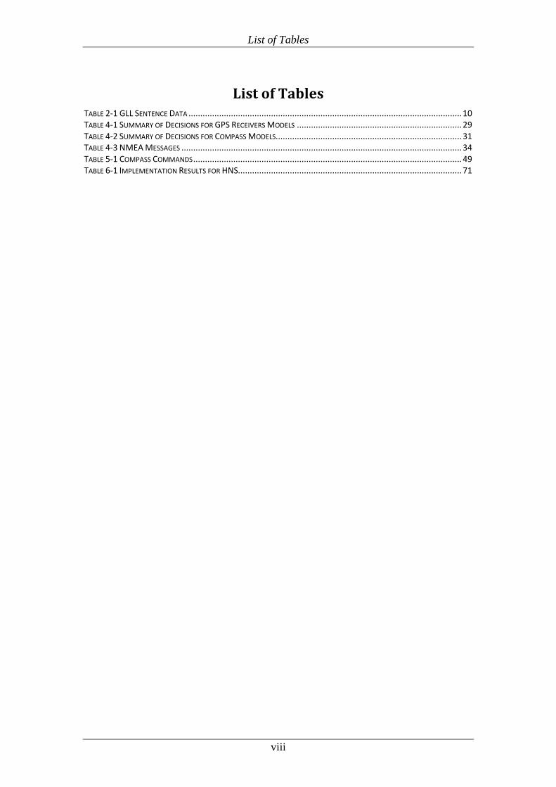
List of Tables
List of Tables TABLE 2-1 GLL SENTENCE DATA .................................................................................................................... 10 TABLE 4-1 SUMMARY OF DECISIONS FOR GPS RECEIVERS MODELS ...................................................................... 29 TABLE 4-2 SUMMARY OF DECISIONS FOR COMPASS MODELS............................................................................... 31 TABLE 4-3 NMEA MESSAGES ....................................................................................................................... 34 TABLE 5-1 COMPASS COMMANDS .................................................................................................................. 49 TABLE 6-1 IMPLEMENTATION RESULTS FOR HNS............................................................................................... 71
viii
Introduction
1 Introduction Over the years, development of various types of navigational aids has been increased rapidly and Handheld Navigation (HN) is one of the most commonly used navigational techniques. The goals of all the navigation systems are the same i.e. to determine the precise current position and the direction to the destination. The development of advanced technologies makes it possible to create new navigation facilities. Moreover, these technologies give the capabilities to the system (robot, car etc) to steer themselves without human intervention. Computers and microcontrollers have become very powerful over the last decades. The use of microcontrollers in navigational systems has increased also. Today, microcontrollers, GPS receivers and compasses can be found almost everywhere around us, e.g. in cars, agricultural machines, airplanes and mobile phones, etc.
1.1 Motivation for two designs Over the years, development of various types of navigational aids has been increased rapidly and Handheld Navigation (HN) is one of the most commonly used navigational techniques. The goals of all the navigation systems are the same i.e. to determine the precise current position and the direction to the destination. The development of advanced technologies makes it possible to create new navigation facilities. Moreover, these technologies give the capabilities to the system (robot, car etc) to steer themselves without human intervention. Computers and microcontrollers have become very powerful over the last decades. The use of microcontrollers in navigational systems has increased also. Today, microcontrollers, GPS receivers and compasses can be found almost everywhere around us, e.g. in cars, agricultural machines, airplanes and mobile phones, etc.
1.2 Handheld Navigation System (HNS)
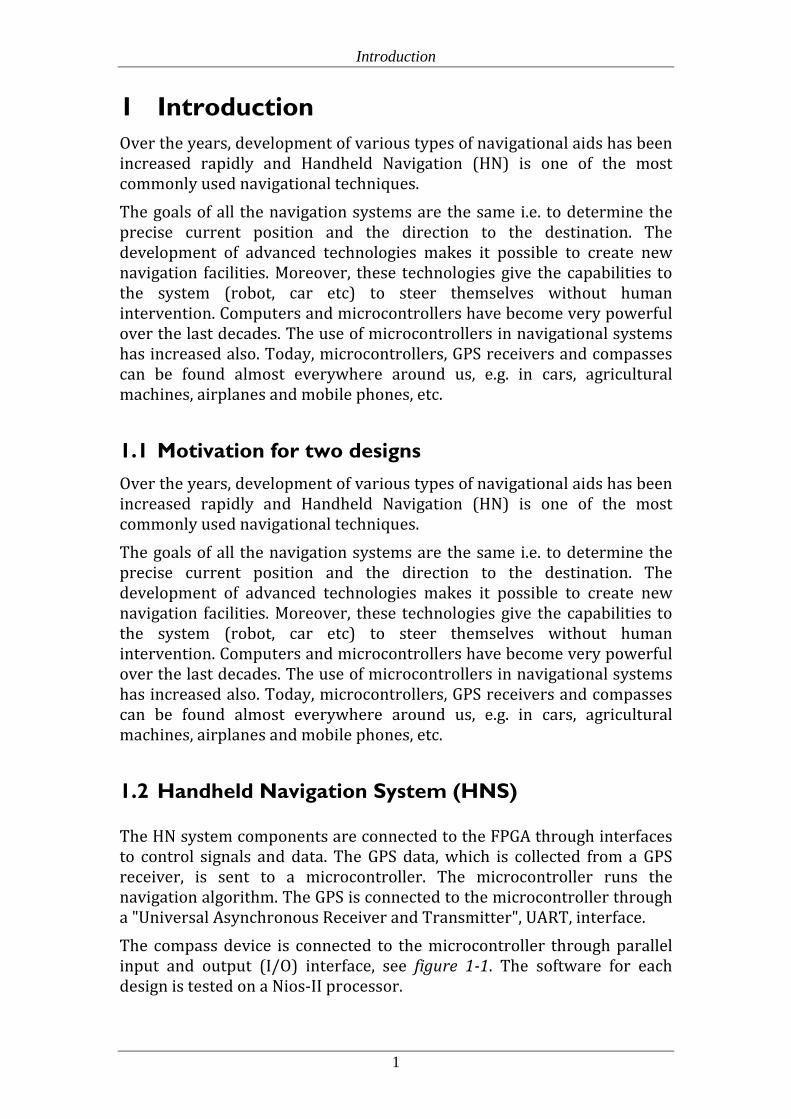
The HN system components are connected to the FPGA through interfaces to control signals and data. The GPS data, which is collected from a GPS receiver, is sent to a microcontroller. The microcontroller runs the navigation algorithm. The GPS is connected to the microcontroller through a "Universal Asynchronous Receiver and Transmitter", UART, interface. The compass device is connected to the microcontroller through parallel input and output (I/O) interface, see figure 1-1. The software for each design is tested on a Nios-II processor.
1
Introduction
Therefore, we decided to design and prototype a Handheld Navigation (HN) system on an Altera FPGA board. In order to achieve thesis goal, the first step was to perform general and analytical analysis of HN system, distance and direction. To perform prototyping, the second step was to Create HN “PCB” board and to develop the software. The next step was the specification of the HN design. After that the interface between HN and Nios II processor was specified. The performance of the design was evaluated through implementation. The last step was to make a prototype of the designed HN on an Altera FPGA board. Performance was evaluated based on navigation track analysis. .
Compass
GPS
HN board (PCB)
GPS-UART protocol
Embedded System
Nios II System
Compass interface
Figure 1-1 HNS System Design Schematic
1.3 Purpose and Aims In the thesis work, there is a comparison between the resulting tracks from different types of a hand held navigation device when used during walking between a start position and a destination position. The paths shall include different types of obstacles. The assumption is that a device that has a digital compass is better in finding the actual walk direction than a system that must rely on that the GPS receiver is moving so the direction can be found from track points. The main goal is to verify this assumption. A flexible Hand Held navigation device shall be designed. It shall include a programmable microcontroller and different types of sensors e.g. GPS module and digital compass. It shall also have a pointing device, e.g. a display, and a SD card for track records. In order to achieve the goal for the thesis, two prototype designs shall be created. The design decisions must consider suitable ways to calculate an accurate relative direction angle to the destination. By selecting the accurate components (GPS, compass and microcontroller) for the hardware designs and developing the software we hope to achieve this
2

Introduction
goal. The first method is used to calculate the relative direction angle from just GPS track points. The second method is used to calculate the relative direction angle by using GPS receiver track points and compass angle. The developed system shall be tested in different environments and the track points shall be recorded for off line evaluation of the different tracks from start position to destination position.
1.4 Limitations There are some limitations of our design; first we cannot move with HN-System easily in our hand because it consists of two hardware parts (Altera DE-2 Board, HN-Board), if we move with the complete system it will be malfunction because of the loss connections. If we design the whole system on one Compaq PCB with a standalone microcontroller and a small battery then it will be easy to move with the whole system without any disturbance.
1.5 Outline The remaining part of the thesis report is divided into the following chapters. In Chapter 2, a theoretical background is given, which includes a brief explanation of the components of HN designs. It also discusses the description of the hardware and development tools that will be used to prototype the HN system. Chapter 3 starts with a description of the suitable methodology for this thesis. Chapter 4 briefly describes the design specification and the overall design decisions for the components of the designs are presented. Chapter 5 describes the complete design and internal structures of the HN for coordinates, distance and direction. Chapter 6 presents the prototyping of HN designed on FPGA board. The testing designs describe how software and hardware are tested. The achieved results are drawn, presented and discussed. Chapter 7 is the final chapter. It has a conclusion of thesis and possible future work is discussed.
3

Theoretical Background
2 Theoretical background This chapter describes the relevant theoretical background about the area of Handheld Navigation (HN) design. It starts with describing the components and interface protocol used for the developed system. Moreover, it provides a brief description of the components used in prototype design, e.g. GPS receiver, compass, the implementation environment and characteristic technologies which have been investigated which have been investigated. Some details about programmable hardware and tools for prototyping will be discussed.
2.1 Global Position System (GPS) The Global Positioning System (GPS) is a system most commonly used worldwide for navigation; it completes two circles around the earth. The GPS system is owned, operated and developed by the US Department of Defence (DOD). The Global Position System consists of three main segments (space segment, control segment and user segment). The space segment is consisting of 28 operational satellites and they are distributed into six orbits. These are inclined at an angle of 55° to the equator orbit of the earth. Each satellite is complete one circle around the Earth twice a day. The satellite height from the earth is 20180 kilometres. Each satellites contains of four precise atomic clocks. The control segment is managing the space segment and atomic clock process. The user segment (GPS receiver) provides continuous data (positioning, time, speed and directions of the travel) when there are enough satellite signals available [1]. A simple illustration is shown in figure 2-1. The GPS benefit users around the world. The GPS is use in many different fields, including air, road, marine, rail navigation, telecommunications, emergency response, oil exploration, agriculture equipment, mining, etc.
User
1575.42 MHzBPSKPRN (50Hz + 1023 MHz C/A code)
GPS
Satellite-5
Satellite-12
Satellite-7
Satellite-21
Satellite-3
Satellit
e-15
Figure 2-1 Global Positioning System
4

Theoretical Background
2.1.1 GPS Function
Every satellite contains a computer and four atomic clocks and it broadcasts its own position, current time label and other data for the satellite. A GPS receiver calculates the time difference between transmission and reception by subtracting the arrival time label (recorded from its internal clock when transmitted) called transit time (τ). The distance (d) between satellite and receiver can be calculated by multiplying the signal travel time with speed of light (3*108 m/s), see formula 2-2.Therefore, the time for a signal to reach the earth surface is approximately (67.3 ms) directly under the satellite.
𝐝𝐝𝐝𝐝𝐝𝐝𝐝𝐝𝐝𝐝𝐝𝐝𝐝𝐝𝐝𝐝 = 𝐝𝐝𝐭𝐭𝐝𝐝𝐝𝐝𝐝𝐝𝐝𝐝𝐝𝐝 𝐝𝐝𝐝𝐝𝐭𝐭𝐝𝐝 × 𝐝𝐝𝐬𝐬𝐝𝐝𝐝𝐝𝐝𝐝 𝐨𝐨𝐨𝐨 𝐥𝐥𝐝𝐝𝐥𝐥𝐥𝐥𝐝𝐝(𝐝𝐝) (2-1)
𝐝𝐝 = 𝛕𝛕 × 𝐝𝐝 (2-2)
The GPS receiver can see a number of satellites in space. The number is depending on the receiver and strength of satellite signal. At minimum four satellites’ signals must be received concurrently in order to calculate the position, speed and time accurately, the GPS positioning is shown in figure 2-2.
distance
distance
distancedistance
User
position
Satellite
SatelliteSatellite
Satellite
1
n SpreadSignal
Process
RF amp.Mixer
A/D Con.
Ref. Osc.Mic.
Controller
M. RAM &ROM
2MHz
Signal Processor(Calculation)
TTL Level I nterface
DGPS
Power supply3.3-5V
GPS receiverRF
Stage
1575.42MHz
Figure 2-2 Global Positioning System
As shown in the figure above, the receiver’s position can be calculated whenever determining four satellites’ locations and ranges from the GPS receiver. But in the reason of the imprecision of clocks the range measurements could be very much incorrect. The atomic clock of each satellite updates regularly by the control segment. The atomic clock is very accurate but the local clock in the receiver can shift for several reasons. Local clock in the receiver might have varying drift rates
5

Theoretical Background
which are influenced by different environmental conditions such as, a change in the ambient temperature or a change in the voltage level that is applied to a crystal resonator. E.g. if we consider that a local clock is off for 0.1 microseconds for any reason, the error range would be 30 meters too long. The fourth satellite measurement is essential to correct the receiver’s internal clock. Adding more satellite signals into consideration can increase the accuracy. The sources of error in the global position system are atmosphere medium, satellite clock offset and electronics signal offset and GPS clock offset. The normal reception of a civilian GPS receiver can have positioning accuracy in a few metres range [2].
2.1.2 GPS Signal Description
The Global Position System consists of three main segments (Space Segment, Control Segment and User Segment). The satellite navigation systems work by triangulating a user's location from known location reference transmitters via four visible satellites in three dimensions (3D). The group of 28 satellites orbits the Earth in a medium earth orbit. The satellite broadcast signal contains data, which identifies the satellite and provides the positioning, timing, satellite status and corrected orbit parameters of the satellite. At the time the locations are known for each of the available satellites in vision, the receiver can then determine its location by calculating distances to each satellite from the time-of-flight of the information bits for that satellite's message, as shown in figure 2-2. The currently available GPS signal is called the Coarse/Acquisition (C/A) code. The satellites are broadcasting own position and current time label. GPS satellites transmit on two frequencies; known as L1 (1575.42 MHz) and the other at L2 (1227.60 MHz). These signals contain the message information with the broadcasting satellite's (orbital parameters i.e. called ephemeris, an atmospheric correction model and a set of course satellite positioning guidelines for all satellites known as the almanac) and more explaining in message structure, see figure 2-3. The broadcast signals are encoded with a Code Division Multiple Access (CDMA) scheme such that all satellites can broadcast concurrently on the same frequency. The data signal is then mixed with the L1 carrier frequency and transmitted. The CDMA encoding scheme uses Pseudorandom Noise (PRN) code sequences known as gold codes. Gold codes are the maximum length sequences with very good cross correlation characteristics. This is allowed for simple signal separation of individual signals by the GPS receiver. Data stream is encoded with a given code (referred to its pseudorandom number code, or PRN code) that can be transmitted at the same time as another. Later the signal recovered by correlating it with that same code. The codes used for the L1 C/A code are 1023 bits long and transmitted at a rate of 1.023 MHz b/s.
6

Theoretical Background
Navigation Message Structure The complete message of the satellites has 25 frames (pages) and it consists of 37500 bits. Each frame has five sub-frames. The transmitted message is a continuous operation of information, sending from the satellite to the receiver at 50 bps. The structure of the satellite message is containing a 1500 bit long frame containing five sub-frames. It takes 30 second to transmit to the receiver. The message’s information contained in each sub-frame and the length of the sub-frame is 300 bits. It is divided into ten words and it is transmitted every 6 seconds. The position and time information of the satellite itself will be sent in every frame (in sub-frame 1-3), which repeats after every 30 seconds. The sub-frame 4 and 5 contains the almanac data for the satellites. The GPS must have the almanac data at least one time [1]. So a complete data message will require the transmission of 25 full frames and it takes 12.5 minutes. The GPS receivers generally receive the message in at least in 40-45 seconds because it requires to receive at least four complete satellite messages, figures 2-3 illustrate the message content and format overview.
Satellite colock correction &Health data
Ephemeris Data 1
Ephemeris Data 2
Other data (ionospher, utc,etc)
Almanic Data for all satellites
One subframe = 300 bits, 6 Seconds
One data
frame =
1500 bits, 30
sec.
Subframe
1
2
3
4
5
Figure 2-3 GPS Message Structure
Transmission of data The GPS receives the Radio Frequency (RF) L1 (1575.42 MHz) signal which is the common carrier frequency for civilian users. L2 (1227.60 MHz) data signal is the common carrier frequency for military users [3]. The encrypted signal is generally used by the military. The satellites signals are modulated by Binary Phase Shift Keying (BPSK) to change or modulate the phase of a carrier wave, as shown in figure 2-4. A suitable receiver can recognize this phase shift and the data can be stored. The GPS channel bandwidth is approximately 2 MHz. The strength of the GPS signal is between -160 ~ -155 dBm.
7

Theoretical Background
Carrier
Data
Signal
Figure 2-4 Binary Phase Shift Keying
Satellite Signal The navigation signals are transmitted in pseudo-random noise (PRN) code sequence, which is the module-2 adding to the 50Hz navigation message data and the Coarse/Acquisition (C/A) code. C/A code is a 1023 bits pseudo random codes broadcasting at 1.023 MHz b/s, repeating every millisecond. The modulation format is BPSK. Figure 2-5 can show the satellite signals generation.
+
××
+
× L2 Signal
L1 carrier 1575,42 MHz
L2 carrier 1227,6 MHz
C/A code 1.023 MHz
Navigation data 50 Hz
P-code 10.23 MHz
L1 Signal 1575,42 MHz
BPSK
Module-2
Figure 2-5 Satellite Signals Generation
Every satellite transmits its unique course/acquisition (C/A) code in the same L band frequency. Every C/A code is generated via different phase selector but using the same basic code generator. The Code Division Multiple Access is used to reduce the interference between the signals from different satellites. GPS Modernization A GPS modernization project includes new ground stations and new satellite goals to offer improved navigation services, three new navigation signals L1C, L2C and L5. L1C uses L1 frequency band but increases signal power by 1.5dB. L2C is uses L2 frequency band, transmitted in higher bit rate (10.23 MHz) and stronger signal. This development in the GPS system allows the GPS receivers to
8

Theoretical Background
acquire 10 times more accuracy than using L1C and also reduces power consumption, whereas the Full Operational Capability (FOC) is expected to be achieved in 2015. The L1C and L2C frequency receiver can have positioning errors approximately one centimetre. L5 (1176.45 MHz) signal will reach FOC in 2019.
2.2 World Geodetic System (WGS 84) WGS-84 is an abbreviation for “World Geodetic System 1984”. It is a standard to determine the coordinates of the earth. Mainly the GPS receiver uses the WGS-84 in calculation and display. The WGS 84 coordinate system is a three dimensional, right-handed, Cartesian coordinate system with its original coordinate point at the Centre of mass (is geocentric) of an ellipsoid which approximates the total mass of the Earth. The standard describes the Earth with a mathematical model. The coordinates of a position in WGS84 are specified in latitude and longitude. Coordinates on the north side (N) and east side (E) become positive and on the south side (S) and west side (W) become negative. Coordinates on the west side become negative and on the east side becomes positive [2].
2.3 GPS Software Interface National Marine Electronics Association Standard (NMEA 0183) NMEA 0183 is a standard protocol produced by the National Marine Electronics Association, an organization in the United States (US). NMEA is for communication between marine devices. It is defined for multiple transmitters and receivers and for serial communication. NMEA standard is defined for sending data in clear text in ASC II characters. The protocol consists of messages that contain information about the type of instrument that transmits manufacturers and information data. All messages have the information to predetermine locations. All device categories such as GPS and computers have their own standard messages’ information [5]. Each NMEA message begins with a dollar sign "$" followed by the name of the message, data, information arranged in groups and then ends with a checksum followed by a newline. The checksum field consists of a "*" and two hex digits representing the exclusive OR of all characters between, but not including, the "$" and "*". To distinguish the information for it is a comma between each information group. The accuracy of the information in a message may vary. All the standard sentences have a two-letter prefix that defines the device that uses that sentence type, e.g. the GPS receiver’s prefix is GP. This is followed by a three-letter sequence that defines the sentence contents (GLL, RMC…). See table 2-1, as an explanation example of NMEA message contents.
9

Theoretical Background
NMEA Message: $GPGLL,A,2503.6319,N,12136.0099,E ,053740.000,A,A*52
Name Example Units Description
Message ID $GPRMC RMC protocol header
Latitude 2503.6319 ddmm.mmmm
N/S Indicator N N=north or S=south
Longitude 12136.0099 12136.0099
E/W Indicator E E=east or W=west
UTC Time 053740.000 hhmmss.sss
Status A A=data valid or V=data not valid
Mode A A=autonomous, D=DGPS, E=DR
Checksum *52
<CR><LF> End of message termination
Table 2-1 GLL Sentence Data
2.4 Harversine Formula
Harversine formula is an important equation in navigation. The formula is used to calculate great circle distance between two points on a sphere from their longitudes and latitudes [8]. The calculation result is, the shortest distance over the earth’s surface. The earth is actually roughly ellipsoidal, therefore the normal formulae to calculate distance and direction from Latitudes and Longitudes between points, can be carried out by using Harversine formula which is shown in equations 2-8, 2-9 below: 𝐑𝐑 = 𝟔𝟔𝟔𝟔𝟔𝟔𝟔𝟔𝐭𝐭 (𝐄𝐄𝐝𝐝𝐭𝐭𝐝𝐝𝐥𝐥 𝐭𝐭𝐝𝐝𝐝𝐝𝐝𝐝𝐢𝐢𝐝𝐝) (2-3) ∆𝒍𝒍𝒍𝒍𝒍𝒍 = 𝐥𝐥𝐝𝐝𝐝𝐝𝐥𝐥 − 𝐥𝐥𝐝𝐝𝐝𝐝𝐥𝐥 (2-4)
∆𝐥𝐥𝐨𝐨𝐝𝐝𝐥𝐥 = 𝐥𝐥𝐨𝐨𝐝𝐝𝐥𝐥𝐥𝐥 − 𝐥𝐥𝐨𝐨𝐝𝐝𝐥𝐥𝐥𝐥 (2-5)
𝐝𝐝 = 𝐝𝐝𝐝𝐝𝐝𝐝𝐥𝐥 ∆𝐥𝐥𝐝𝐝𝐝𝐝𝐥𝐥 + 𝐝𝐝𝐨𝐨𝐝𝐝(𝐥𝐥𝐝𝐝𝐝𝐝𝐥𝐥) × 𝐝𝐝𝐨𝐨𝐝𝐝(𝐥𝐥𝐝𝐝𝐝𝐝𝐥𝐥) × 𝐝𝐝𝐝𝐝𝐝𝐝𝐥𝐥 ∆𝐥𝐥𝐨𝐨𝐝𝐝𝐥𝐥
𝐥𝐥 (2-6)
𝐝𝐝 = 𝐥𝐥 × 𝐝𝐝𝐝𝐝𝐝𝐝𝐝𝐝𝐥𝐥(√𝒍𝒍,𝐥𝐥 − 𝒍𝒍) (2-7)
𝐝𝐝 = 𝐑𝐑 × 𝐝𝐝 (2-8)
10

Theoretical Background
By using the direction formula we can calculate the initial direction to the destination. Which if following the result of this equation, it will be guide as in a straight line along a great circle arc from start point coordinate (lat1, long1) to the target coordinate (lat2, long2) and that will show the direction angle from the start point to the destination point: The formula is:
𝜽𝜽𝑮𝑮𝑮𝑮𝑮𝑮 =𝒍𝒍𝒍𝒍𝒍𝒍𝒕𝒕𝐥𝐥(𝒔𝒔𝒔𝒔𝒕𝒕(∆𝐥𝐥𝐨𝐨𝐝𝐝𝐥𝐥)× 𝒄𝒄𝒄𝒄𝒔𝒔(𝐥𝐥𝐝𝐝𝐝𝐝𝐥𝐥),𝒄𝒄𝒄𝒄𝒔𝒔(𝐥𝐥𝐝𝐝𝐝𝐝𝐥𝐥)×𝒔𝒔𝒔𝒔𝒕𝒕(𝐥𝐥𝐝𝐝𝐝𝐝𝐥𝐥)−𝒔𝒔𝒔𝒔𝒕𝒕(𝐥𝐥𝐝𝐝𝐝𝐝𝐥𝐥)×𝒄𝒄𝒄𝒄𝒔𝒔(𝐥𝐥𝐝𝐝𝐝𝐝𝐥𝐥)×𝒄𝒄𝒄𝒄𝒔𝒔(∆𝐥𝐥𝐨𝐨𝐝𝐝𝐥𝐥))
(2-9) In the formulas above, lat2 is latitude for target coordinates, long2 is the longitude of the target coordinates, lat1 is the latitude of the starting coordinates, long1 is the longitude of the starting coordinates, and with figure 2-6 we can see the GPS direction (θGPS).
North
Destination (Lat2,Long2)
Current point (Lat1,Long1)
θDir. θCurrent
θGPS
Figure 2-6 GPS Direction Angle (θGPS)
2.5 Electronic Compass
The electronic compass is a flux-gate vector magnetometer the earth magnetic field is a three-dimensional field, the X-Y component of the field vector lies parallel to the earth surface and points towards the magnetic north pole. For a latitude not close to the equator the majority of the earth magnetic field lies along the Z-axis and points at the northern hemisphere into the ground. However, the horizontal direction of the earth field is always pointing toward magnetic north and is used to determine the compass direction. Because of this the compass has to be held parallel to the earth’s surface or has to be gimbaled in order to be accurate. Hence, a two-axis magnetometer held parallel to the earth surface is the minimum configuration for magnetic compass.
11
Theoretical Background
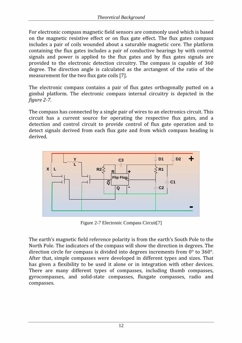
For electronic compass magnetic field sensors are commonly used which is based on the magnetic resistive effect or on flux gate effect. The flux gates compass includes a pair of coils wounded about a saturable magnetic core. The platform containing the flux gates includes a pair of conductive bearings by with control signals and power is applied to the flux gates and by flux gates signals are provided to the electronic detection circuitry. The compass is capable of 360 degree. The direction angle is calculated as the arctangent of the ratio of the measurement for the two flux gate coils [7].
The electronic compass contains a pair of flux gates orthogonally putted on a gimbal platform. The electronic compass internal circuitry is depicted in the figure 2-7.
The compass has connected by a single pair of wires to an electronics circuit. This circuit has a current source for operating the respective flux gates, and a detection and control circuit to provide control of flux gate operation and to detect signals derived from each flux gate and from which compass heading is derived.
-
+YL
X L
D1 D2
C1C2
C3
R1R2 R +
Flip Flop
-
Figure 2-7 Electronic Compass Circuit[7]
The earth’s magnetic field reference polarity is from the earth’s South Pole to the North Pole. The indicators of the compass will show the direction in degrees. The direction circle for compass is divided into degrees increments from 0° to 360°. After that, simple compasses were developed in different types and sizes. That has given a flexibility to be used it alone or in integration with other devices. There are many different types of compasses, including thumb compasses, gyrocompasses, and solid-state compasses, fluxgate compasses, radio and compasses.
12
Theoretical Background
2.6 Prototyping Embedded Systems This section described about the platform used for designing the HN system. The Nios II software, Altera DE-2 board and Quartus II software are used for prototyping the system an introduction to this hardware and described in the following paragraphs.
2.6.1 DE2 Development Board
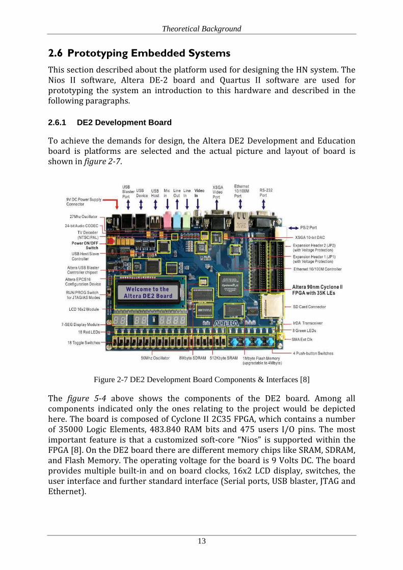
To achieve the demands for design, the Altera DE2 Development and Education board is platforms are selected and the actual picture and layout of board is shown in figure 2-7.
Figure 2-7 DE2 Development Board Components & Interfaces [8]
The figure 5-4 above shows the components of the DE2 board. Among all components indicated only the ones relating to the project would be depicted here. The board is composed of Cyclone II 2C35 FPGA, which contains a number of 35000 Logic Elements, 483.840 RAM bits and 475 users I/O pins. The most important feature is that a customized soft-core “Nios” is supported within the FPGA [8]. On the DE2 board there are different memory chips like SRAM, SDRAM, and Flash Memory. The operating voltage for the board is 9 Volts DC. The board provides multiple built-in and on board clocks, 16x2 LCD display, switches, the user interface and further standard interface (Serial ports, USB blaster, JTAG and Ethernet).
13

Theoretical Background
FPGA Architecture Field Programmable Gate Arrays (FPGA) is feasibly the evolution of technology on high level for the embedded system. An FPGA is a device that is optimized for configurability. The FPGA is able to emulate the functionality of any digital design. Altera FPGA Cyclone II is consisting of programmable logic, interconnections, DSPs, memory blocks and other extra features as shown in the figure 2-8. It shows a circuit with 36 logic blocks (LB) distributed in perpendicular style (horizontal and vertical). Cyclone II is low cost FPGA device family. It contains 68,416 logic elements (LE), 622 useable I/O pins and 1.125 M-bits of embedded memory, Phase-Locked Loops (PLLs) and Multipliers [10] [11]. Usually a FPGA consists of two main parts, routing and logic blocks (LB). The architecture of FPGA logic block is different within different families even for the same company.
Q
QSET
CLR
S
R
Q
QSET
CLR
S
R
Q
QSET
CLR
S
R
Q
QSET
CLR
S
R
Q
QSET
CLR
S
R
Q
QSET
CLR
S
R
Q
QSET
CLR
S
R
Q
QSET
CLR
S
R
Q
QSET
CLR
S
R
Q
QSET
CLR
S
R
Q
QSET
CLR
S
R
Q
QSET
CLR
S
R
Q
QSET
CLR
S
R
Q
QSET
CLR
S
R
Q
QSET
CLR
S
R
Q
QSET
CLR
S
R
Q
QSET
CLR
S
R
Q
QSET
CLR
S
R
Q
QSET
CLR
S
R
Q
QSET
CLR
S
R
Q
QSET
CLR
S
R
Q
QSET
CLR
S
R
Q
QSET
CLR
S
R
Q
QSET
CLR
S
R
Q
QSET
CLR
S
R
Q
QSET
CLR
S
R
Q
QSET
CLR
S
R
Q
QSET
CLR
S
R
Q
QSET
CLR
S
R
Q
QSET
CLR
S
R
Q
QSET
CLR
S
R
Q
QSET
CLR
S
R
Q
QSET
CLR
S
R
Q
QSET
CLR
S
R
Q
QSET
CLR
S
R
Q
QSET
CLR
S
R
Q
QSET
CLR
S
R
Q
QSET
CLR
S
R
Q
QSET
CLR
S
R
Q
QSET
CLR
S
R
Q
QSET
CLR
S
R
Q
QSET
CLR
S
R
Q
QSET
CLR
S
R
Q
QSET
CLR
S
R
Q
QSET
CLR
S
R
Q
QSET
CLR
S
R
Q
QSET
CLR
S
R
Q
QSET
CLR
S
R
Q
QSET
CLR
S
R
Q
QSET
CLR
S
R
Q
QSET
CLR
S
R
Q
QSET
CLR
S
R
Q
QSET
CLR
S
R
Q
QSET
CLR
S
R
Q
QSET
CLR
S
R
Q
QSET
CLR
S
R
Q
QSET
CLR
S
R
Q
QSET
CLR
S
R
Q
QSET
CLR
S
R
Q
QSET
CLR
S
R
Q
QSET
CLR
S
R
Q
QSET
CLR
S
R
Q
QSET
CLR
S
R
Q
QSET
CLR
S
R
Q
QSET
CLR
S
R
Q
QSET
CLR
S
R
Q
QSET
CLR
S
R
Q
QSET
CLR
S
R
Q
QSET
CLR
S
R
Q
QSET
CLR
S
R
Q
QSET
CLR
S
R
Q
QSET
CLR
S
R
IOBLB contact wires
Figure 2-8 FPGA Overview
The logic block is connected to one another in an array of wires and contacts. In the circuit there are a number of I/O pads. This multiplicity of embedded cores have involved engineers and made FPGAs become one of the most important devices of carry out digital systems. It supports Nios II processor. Multiple Nios II processors can also be used in a design with this family device and supports power-on-reset. Large complex digital systems can also be implemented. Multiple communication modes such as JTAG, passive serial and active serial are supported. Cyclone II FPFA has been used in Automobile, Communication Technology and Video Processing Systems. The major advantage of FPGA is the ability of re-programming, rapid prototyping and development easily.
14

Theoretical Background
Logic block
The Logic Block (LB) is a group of blocks where the functionality is carried out. The LB is consisting of many smallest units called logic elements (LE). The logic blocks can be configured to perform the simple logic gates AND, OR, XOR etc or complex combinational functions such Adder, Multiplexer, decoder, etc. The logic elements contain a number of the LUTs (Lock up Table) which generator can implement any function of four variables (as a RAM). Moreover, LEs contain a programmable register and carries a chain with carry select capability. LUT is a simple storage element and can implement Boolean function. The size of LUTs can affect the resource utilization within block [10]. Each LE can drive a high number of other LEs through local and direct interconnects. By increasing the number of inputs, it can enhance the possible functions, which could be implemented but will also increase the delay. The 4-input LUT is ideal in term of area and delay, see figure 2-9.
4-Input LUT D Flip
Flop
A
DCB Z
Clock
Figure 2-9 Block Diagram of LE
The Logic Elements are operating in two types of modes. Normal mode is suitable for general logic application and combined functions. Arithmetic mode is ideal for carry out adders, counters, accumulators and comparators. Logic blocks are known as adaptive logic modules (ALMs), when the logic block is of more complex design with special embedded addition logic. ALM is the key to become high-performance and area-efficient architecture. Each ALM is 8-input and it consists of 2-adaptive LUTs. The adaptive LUT was improved to have the capacity to share LUT-masks between functions and resulting in the final design of the 8-input allowing the ALM to implement the ordinary 4-input functions and also any function with up to 6-input and some 7-input functions [10] [11]. The ALM contains of two programmable registers, two dedicated full adders, a carry chain, shared arithmetic chain, and a register chain. The FPGA components are often called Intellectual Property (IP). In addition, the components can be designed and describe the functionality of the FPGA by using a hardware describing language (HDL), like Verilog or VHDL.
15

Theoretical Background
NIOS-II processor core
Nios-II processor is a user configurable 32 bit Reduced Instruction Set Computer (RISC) soft core processor. The architecture uses separate instruction and data buses, which are often called the Harvard architecture, see figure 2-10. Nios-II IDE is a graphical software development tool for programming the Nios II processor [11]. The Nios-II architecture supports a flat register file consisting of 32-bit general-purpose integer registers, 32-bit control registers and software Integrated Development Environment (IDE) and etc. IDE provides Eclipse tool environment. After writing a program for Nios II, it is built and run. JTAG download cable is the communication medium for Nios II processor. Nios-II provides a set of peripherals like on chip memory, UART, SRAM, SD-card etc. The flexibility to add features and enhance performance of the Nios II processor system makes it easier to use. The Nios-II Software is based on the GNU C/C++ compiler. It provides a familiar and established environment for software development. The processor can be created in the System on-a-programmable-chip (SOPC) builder tool using Nios-II with peripherals. Nios-II is connected with other peripherals through Avalon bus. More than one CPU can be used in one project depending on the request of the system.
Program controller
and Address
generation
Exception Controller
Interrupt Controller
JTAGDebug Module
Custem Instruction
Logic
Arthmetic Logic Unit (ALU)
Instruction Cashe
Data Cashe
Control Registers ctl0 to ctl4
GeneralPurpose Registers r0 to r31
JTAG contactSoftware debugger
CostomI/O Signal
ResetClock
NiosII Process Core
Instruction Master Port
Data Master Port
Irq(31..0)
Figure 2-10 Nios-II Processor Core [11]
There are three types of CPU: ″Economic″, ″Standard″ and ″Fast″, which acquire different portions of hardware resources and behave in different performance that is chosen according to demands:
1- NIOS-II/e is called an economy core. This is designed to achieve the smallest possible core size.
16

Theoretical Background
2- NIOS-II/s is the standard core. This is designed to achieve the small possible core size.
3- NIOS-II/f is the named a fast core. This is designed for high execution performance.
Quartus-II FPGA Design Tool
The Quartus-II software includes solutions for the different phases of FPGA design. It has tools available for design synthesis, implementation and simulation using VHDL or Verilog. This design software consists of a multi-platform design environment that can adapt to the employer’s exact design requirements [12]. The Quartus-II software allows the designer to use the graphical user and command-line interface for each phase of the design flow, as shown in figure 5-11. It is possible to use one of these interfaces for the entire flow, or use different options at different phases.
Design EntryIncludes block based design,
System level design and software development
Synthesis
Place & Route
Timing Analysis
Simulation
Programing & Configration
Power Analysis
Debugging
Engineering Change
Management
Timing Closure
Figure 2-11 Quartus-II Design Flow [12]
The Quartus-II flow consists of the following steps:
• Design Entry - - the desired design module is specified either by a schematic diagram, a text file using a hardware description language Verilog HDL or VHDL or a block and generated in SOPC builder tool.
17
Theoretical Background
• Synthesis- Compiling the design circuit checks the errors and at the end gives a summary of compilation results.
• Place and route- the design blocks are the placed and routed into the target device.
• Timing Analysis - In this the step is analyzed and reported timing information to provide an indication of the expected performance of the design.
• Simulation- Fitted the behavior of design to verify both its functional correctness and context of real time sign.
• Programming- The design files are downloaded into FPGA through the USB blaster cable communication link between PC and DE2 board.
SOPC Builder
The SOPC (System-On-a-Programmable-Chip) Builder is a system development tool for creating systems based on processors, peripherals, memories and communication interfaces like JTAG UART, SD-card, UART, and SPI etc. SOPC is divided into two parts, first is graphical users interface (GUI) and the second is generating program. SOPC Builder enables the designer to describe and generate a complete SOPC, and in a system design is involved as part of the Quartus-II. The SOPC Builder automates the task of integrating hardware components. SOPC builder helps the designers to fast and easily construct a system level project [13].
Devices Interfaces
Parallel Input/Output (PIO)
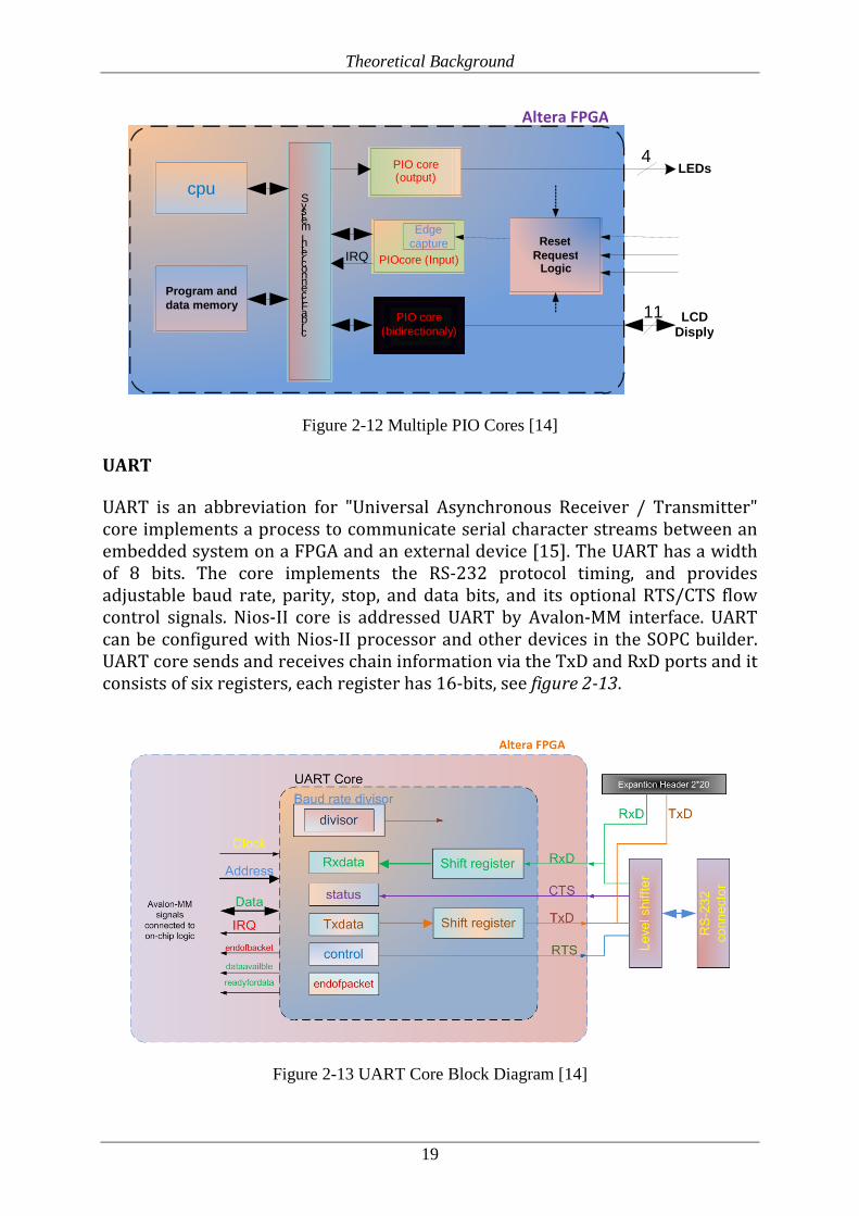
The Parallel Input-Output core is standard interface for Nios-II and its general purpose 32 I/O ports. Nios-II can address PIO through Avalon bus. Via PIOs core can connect a FPGA to control a variety of external devices to reading and writing. The PIO core can be configured with different modes such as input only, output only and bidirectional, as well as support for interrupted requests (IRQs) [14]. Thus, Nios-II core can be connected with an external device to send and receive 32 bits information through Parallel Input/output. Moreover, PIO can be configured and integrated with Nios-II processor and other components in SOPC builder. Multiple PIOs can be connected with Nios-II processor. PIO is interface with Nios-II through Avalon bus as shown in figure 5-12.
18
Theoretical Background
Figure 2-12 Multiple PIO Cores [14]
UART
UART is an abbreviation for "Universal Asynchronous Receiver / Transmitter" core implements a process to communicate serial character streams between an embedded system on a FPGA and an external device [15]. The UART has a width of 8 bits. The core implements the RS-232 protocol timing, and provides adjustable baud rate, parity, stop, and data bits, and its optional RTS/CTS flow control signals. Nios-II core is addressed UART by Avalon-MM interface. UART can be configured with Nios-II processor and other devices in the SOPC builder. UART core sends and receives chain information via the TxD and RxD ports and it consists of six registers, each register has 16-bits, see figure 2-13.
Figure 2-13 UART Core Block Diagram [14]
Reset Request
Logic Program and data memory
S y s t e m I n t e r c o n n e c t F a b r i c
cpu PIO core ( output )
PIO core ( bidirectionaly )
PIOcore ( Input ) IRQ
Altera FPGA
Edge capture
4
11
LEDs
LCD Disply
19

Theoretical Background
Design Memories
On-chip RAM
The On-chip RAM is a fundamental memory to create the simple computer on FPGAs. The on-chip M4K memory blocks are fully synchronous with a 32 bits data width, which means that the input can be registered but the output has probability to be registered or combinatorial. It consists of memory blocks, which are dual port blocks [9]. The on-chip memory is placed as a column in the middle on a FPGA chip. The memory is available as an IP component on SOPC Builder and its can be configured and integrated with Nios-II processor on this Builder. SRAM
In the design, it requires larger than the standard memory (On-Chip Block Memory) to be able to read and write the information from the GPS receiver and compass, and for this purpose we chose the Static Random Memory Access chip (SRAM) instead of On-chip memory (RAM), it is asynchronous CMOS. SRAM memory consists of 6 transistors, 4 transistors are used to store each bit and two transistors are used to control the access to cell-storage during read and write operations [10]. Moreover, the memory is available as IP component on SOPC builder. The memory can be configured and integrated with Nios-II processor on this builder [16]. The SRAM is volatile. If power supply is disconnected during configuration or running mode, these devices will lose stored configuration (program). So an additional non-volatile memory such as flash memory, SD card or EEPROM is required outside to FPGA circuit to store the program. Nios-II processor can handle addressing automatically by Avalon bus. The SRAM memory can be store up to 512 Kbytes and organized as a 16-bit data. The memory frequency is 50 MHz via Avalon bus the FPGA can be accessed and controls its operation. SD-Card The SD card is configured to store data. The Secure Data (SD) card can be used for data a portable, which means that it can be used to save data on it, to be transferred to other devices. Nios-II can address a SD-card through Avalon bus interface [16]. A SD card is a 16-bit File Allocation Table (FAT16) based on a portable drive. The SD Card IP Core can be configured and integrated with Nios-II processor and other devices in the SOPC builder. Moreover, a FPGA can control and access the SD-card through Avalon bus. The SD Card is non-volatile memory such as flash memory or EEPROM. The speed of SD card based FPGA is slower than SRAM based FPGA. The SD-cared diagram is shown in figure 2-14.
20

Theoretical Background
SD Card Interface
Avalon Interface
FSM
B_SD_ cmd
B_SD_ dat
B_SD _dat3
o_SD_ clk
i_Avalon_chip_select
i_Avalon_address[7..0]
i_Avalon_W.datta[31..0]
o_Avalon_R.data[31..0]
i_Avalon_byteenable[3..0]
i_Avalon_waitrequist
i_clk
i_reset
i_reset_n
i_Avalon_read
SD-Card Avalon Interface
Figure 2-14 Block Diagram of SD-Cared [16]
LCD Display
The 16207 LCD is configured and generated with the SOPC builder. Nios-II processor can be addressed to display characters on an Optrex 16207 (or equivalent) 16×2-character LCD panel via Avalon bus [26]. Furthermore, a FPGA can control and access the display through Avalon bus. The LCD has low power consumption enables it to be used in battery-powered electronic equipment. The display has more energy efficient than cathode ray tube (CRT) display. The Optrex 16207 LCD display diagram is shows in figure 2-15.
Optrex 16207LCD Module
Optrex 16207LCD Module
ERSR/W
DB0..7
address
data
control
Altera FPGA
TAvalon-MM slaveinterface toon-chip logicext
Figure 2-15 LCD Display Diagram [25]
21

System Development Methodology
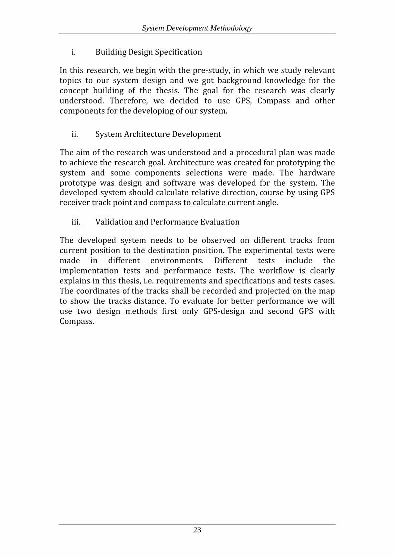
3 System Development Methodology This chapter describes the research methodology used for implementing the HN-System. The implementation method is divided into different segments. For a complete understanding and implementation of our goal the whole system is represented by a flow chart. This flow chart has different parts and each part will be explained to achieve our design goal.
3.1 Research method The concept of a systematic process in research is a technical method, which shall be followed in order to increase our understanding of the occurrence in which we are concerned. “Research method is defining a way of investigating an empirical topic by following a set of pre-specified procedures” [17], figure 3-1 shows the system development research method.
Devloping Design SpcificationApplication Knowledge
System Architecture DsvelopmentTheoretical Background Development relevant to
HNS
Hardware Components
Standard Software
Sotware DevelopmentHarware Design and Prototyoing the System
Validation and Performance EvaluationTest cases
Figure 3-1 System Development Methodology Flowchart
To reach our goal, we followed "System Development Research Method" as shown in figure 3-1. "The system development research approach denotes a way to perform research through exploration and integration of available technologies to produce an artefact, system or system prototype". The steps of the research method were done sequentially [18].
22
System Development Methodology
i. Building Design Specification
In this research, we begin with the pre-study, in which we study relevant topics to our system design and we got background knowledge for the concept building of the thesis. The goal for the research was clearly understood. Therefore, we decided to use GPS, Compass and other components for the developing of our system.
ii. System Architecture Development
The aim of the research was understood and a procedural plan was made to achieve the research goal. Architecture was created for prototyping the system and some components selections were made. The hardware prototype was design and software was developed for the system. The developed system should calculate relative direction, course by using GPS receiver track point and compass to calculate current angle.
iii. Validation and Performance Evaluation
The developed system needs to be observed on different tracks from current position to the destination position. The experimental tests were made in different environments. Different tests include the implementation tests and performance tests. The workflow is clearly explains in this thesis, i.e. requirements and specifications and tests cases. The coordinates of the tracks shall be recorded and projected on the map to show the tracks distance. To evaluate for better performance we will use two design methods first only GPS-design and second GPS with Compass.
23

Design of Handheld Navigation System
4 Design of Handheld Navigation System This chapter starts with general description of different prototypes for the designs and components related to the designs. Finally, the design decisions of Handheld Navigation for accuracy, speed and size are discussed in order to validate the research target.
4.1 Handheld Navigation System Designs(HNSD) The term navigation normally used to express the accurate direction of the traveller i.e. to arrive to the destination. In order to achieve this goal, we are implementing the methods and prototype that will use the better and suitable method for navigation track. There are two methods for calculating the correction directions i.e. difference between target direction and current direction. One method use just GPS and the other is usage the GPS receiver and digital compass. These components are suitable navigation devices to calculate the direction correction to the destination. Assumption, we should know the GPS coordinates of the destination because we don’t have the map or software map. The GPS software map helps the user to use the name of the place instead of the coordinates of the destination.
4.1.1 First Navigation Design
In this thesis, to be able to calculate the directions from GPS (𝜃𝜃𝐺𝐺𝐺𝐺𝐺𝐺), as defined in formula 4-1, a program is created to read and write the information that can be detected from the receiver. The GPGLL signal is one of the GPS messages that have been used to calculate course over ground from the received coordinates. The coordinates received must be converted from ACII strings into decimal numbers and converted to radians, to be able to use the Harversine formula i.e. to estimate the direction and course over ground. The final direction angle”𝜃𝜃𝑑𝑑𝑑𝑑𝑑𝑑1" of the GPS receiver can be calculated by deducting the course over ground " 𝜃𝜃𝑐𝑐𝑐𝑐𝑐𝑐𝑑𝑑" from the" 𝜃𝜃𝐺𝐺𝐺𝐺𝐺𝐺", as shown in formula 4-1, 4-2. 𝜽𝜽𝑮𝑮𝑮𝑮𝑮𝑮 =𝒍𝒍𝒍𝒍𝒍𝒍𝒕𝒕𝐥𝐥(𝒔𝒔𝒔𝒔𝒕𝒕(∆𝐥𝐥𝐨𝐨𝐝𝐝𝐥𝐥)× 𝒄𝒄𝒄𝒄𝒔𝒔(𝐥𝐥𝐝𝐝𝐝𝐝𝐥𝐥),𝒄𝒄𝒄𝒄𝒔𝒔(𝐥𝐥𝐝𝐝𝐝𝐝𝐥𝐥)×𝒔𝒔𝒔𝒔𝒕𝒕(𝐥𝐥𝐝𝐝𝐝𝐝𝐥𝐥)−𝒔𝒔𝒔𝒔𝒕𝒕(𝐥𝐥𝐝𝐝𝐝𝐝𝐥𝐥)×𝒄𝒄𝒄𝒄𝒔𝒔(𝐥𝐥𝐝𝐝𝐝𝐝𝐥𝐥)×𝒄𝒄𝒄𝒄𝒔𝒔(∆𝐥𝐥𝐨𝐨𝐝𝐝𝐥𝐥)) (4-1)
𝜽𝜽𝒄𝒄𝒄𝒄𝒄𝒄𝒄𝒄 =𝒍𝒍𝒍𝒍𝒍𝒍𝒕𝒕𝐥𝐥(𝒔𝒔𝒔𝒔𝒕𝒕(∆𝐥𝐥𝐨𝐨)× 𝒄𝒄𝒄𝒄𝒔𝒔(𝐥𝐥𝐝𝐝𝐝𝐝𝐥𝐥),𝒄𝒄𝒄𝒄𝒔𝒔(𝐥𝐥𝐝𝐝𝟔𝟔)×𝒔𝒔𝒔𝒔𝒕𝒕(𝐥𝐥𝐝𝐝𝐝𝐝𝐥𝐥)−𝒔𝒔𝒔𝒔𝒕𝒕(𝐥𝐥𝐝𝐝𝟔𝟔)×𝒄𝒄𝒄𝒄𝒔𝒔(𝐥𝐥𝐝𝐝𝐝𝐝𝐥𝐥)×𝒄𝒄𝒄𝒄𝒔𝒔(∆𝐥𝐥𝐨𝐨)) (4-2) Where the lat2 is latitude for target coordinates, long2 is the longitude of the target coordinates, lat1 is the latitude of the current coordinates, long1 is the longitude of the current coordinates and la0 is the latitude of the
24

Design of Handheld Navigation System
previous coordinates. To be able to use the direction, it must convert the results from Harversine formula to the degree, and then the final direction is calculated by using the formula 4-3:
𝜽𝜽𝒅𝒅𝒔𝒔𝒄𝒄𝐥𝐥 = 𝜽𝜽𝑮𝑮𝑮𝑮𝑮𝑮 − 𝜽𝜽𝒄𝒄𝒄𝒄𝒄𝒄𝒄𝒄 (4-3)
4.1.2 Second Navigation Design
To calculate the direction in the second design, GPS software has been used to calculate the " 𝜃𝜃𝐺𝐺𝐺𝐺𝐺𝐺" by using the Harversine formula, as mentioned in section 4.1.1. In order to make a compass program to calculate the current direction angle "𝜃𝜃𝐶𝐶𝑐𝑐𝐶𝐶𝐶𝐶" between the points, refer to formula 4-5. The software is designed to reset the compass and to read and write the information by considering MSB, because the compass axes have eleven data bits. The arctan formula for the angle between axes is used to compute the compass current angle. The compass can be calculating the current angle (θComp) by measuring the x and y magnetic field strength measurements (N cosθ, N sinθ), see formula 4-4. Using a couple of trigonometry identities, it turns out that the angle (θ) is the arctangent of (- y/x), see formula 4-5.
𝒍𝒍𝒍𝒍𝒕𝒕𝜽𝜽 = 𝑵𝑵𝒔𝒔𝒔𝒔𝒕𝒕𝜽𝜽𝑵𝑵 𝒄𝒄𝒄𝒄𝒔𝒔𝜽𝜽
= 𝒚𝒚𝒙𝒙 (4-4)
𝜽𝜽𝑪𝑪𝒄𝒄𝑪𝑪𝑪𝑪 = 𝐝𝐝𝐝𝐝𝐝𝐝−𝐥𝐥 𝒚𝒚𝒙𝒙 (4-5)
𝜽𝜽𝒅𝒅𝒔𝒔𝒄𝒄𝐥𝐥 = 𝜽𝜽𝑮𝑮𝑮𝑮𝑮𝑮 − 𝜽𝜽𝑪𝑪𝒄𝒄𝑪𝑪𝑪𝑪 (4-6)
Where: N is magnetic north. The formulas 4-6 above describe how to calculate the final direction angle (𝜃𝜃𝑑𝑑𝑑𝑑𝑑𝑑2) to guide the user of Handheld Navigation to destination.
4.1.3 Performace of two Designs
The aim of this thesis is to present the accurate design that can show the precise direction-angle between current-point and final destination. In comparing the results of correction angles (𝜃𝜃𝑑𝑑𝑑𝑑𝑑𝑑1,𝜃𝜃𝑑𝑑𝑑𝑑𝑑𝑑2) for the designs explained above, we can carry out the tracks by drawing for these two methods, which will be helpful in proving which method should be implement and to be used for finding precise position during travel with Handheld Navigation System.
25

Design of Handheld Navigation System
4.2 Component Selection for Prototyping
4.2.1 GPS Receiver Models
A substantial amount of research has been made to find good GPS modules. The good GPS receiver must have high features that match with the project goal, i.e. good precision, small size, Low power consumption etc. The GPS data and accuracy are affected or degraded by the satellite geometry, electric magnetic interference and multipath. Three suppliers have been selected for the GPS receivers which are U-blox, SparkFun Electronics and Parallax. The selection of receivers will be described in the later sections. U-blox U-blox has several GPS receiver modules [20]. The main differences between the modules are the GPS communication ports and application usage. There are two interesting receivers’ selected NEO-5 module and AMY-5M for study. AMY-5M AMY-5M is the smallest GPS receiver that is highly sensitive in determining location (indoor) and should be soldered directly on PCB. An external antenna is required be used for the best reception. The operating voltage is 1.8 V to 3.0 V and supports by four different serial interfaces. The receiver that features an integrated GPS crystal, providing fast acquisition, high tracking performance at a competitive price and Maximum Update Rate is the 4 Hz. NEO-5D (indoor GPS modules) The NEO-5D module (50 channels) is one of the modern GPS receiver modules. An external antenna is required to be used for the best reception. This receiver has the high performance and developmental technology feature that gives the capability to calculate the accurate indoor positioning. The indoor receiver (NEO-5D) is ROM-based and supports by three different serial interfaces. The time-to-first-fix is less than one second, small size, 1.8 V supply voltage for low power consumption, can be connected to passive patch or active antennas. The tracking sensitivity is -160 dB (Super Sense) which gives high capability to the receiver in determining a precise location. The NEO-5D module provides the position information from 1 to 4 times a second and the accuracy of position is 2.5 m and 2 m with Satellite Based Augmentation GPS System (SBAS).
26

Design of Handheld Navigation System
Spark Fun Electronics GPS Module (08975) The LS20031 GPS Module supports up to 32 channels and outputs at 5Hz and it is one of modern prototypes of the GPS receiver, and the receiver is based on the proven technology found in LOCOSYS 32 channel GPS SMD type receivers MC-1513 that uses MediaTek chip solution [21]. The operating volt is 3.3V. The GPS is supported by a smart antenna receiver which will track up to 32 satellites at a time while providing fast time-to- first- fix and including an embedded antenna with GPS receiver circuits. It´s supported via Built-in micro battery to preserve system data for rapid satellite acquisition and LEDs on GPS circuit board showing the position whether it is fixed or not. The amount of position information from 1 to 5 times per second, low power consumption, The LS20031 GPS module can provide a high sensitivity and excellent performance even in different environment. The serial communication interface is low level TTL. Parallax PMB-248 GPS Receiver and Cable The PMB-248 GPS receiver with serial communication interface TTL and RS-232 can be connected to any micro-controller, a computer and other devices. It is used for robotics, auto pilot, vehicle track, fleet management and for navigation systems. This receiver designed with 12 channels can follow 12 satellites signals at a time. The Signal sensitivity is (-152 dBm) or less and positioning accuracy is about 2m. It has feature of SONY CXD2951GA-4 chipset and built-in rechargeable battery for memory and RTC backup [22]. The Power Consumption typical is 80mA and 3.3V and provides basic performance at a very reasonable cost.
4.2.2 Selection of GPS Receivers
AMY-5M Receiver Its main advantage is its external antenna that helps to place the antenna where one can get the best reception. According to the goal of the thesis the external antenna will reduced the flexibility for the user moving with GPS receiver and also it will requires more space. Therefore, this choice is not good. NEO-5D (indoor GPS modules) NEO-5D is called indoor GPS receiver module. The GPS has a high capability to receive data and determining a precise position. NEO-5D GPS module has the specific process, it is not used for life saving or supporting devices or for aviation. In additions to the external antenna, the user is
27

Design of Handheld Navigation System
able to move freely. Therefore, this GPS receiver is also not suitable for our design. PMB-248 GPS Receiver and Cable The PMB-248 GPS module provides basic performance at a very reasonable cost and a good positioning accuracy is approximately 2 m and it is supported by TTL and RS-232 asynchronous serial communication cable but the signal sensitivity is (-152 dBm) or less and also high power consumption due to these limitations we did not select to use for the implementation of our design. GPS Module (08975) The LS20031 GPS Module is a receiver with a smart antenna. The GPS receiver should be positioned so that the satellite signals are not weakened. The receiver is based on the proven technology found in LOCOSYS 32 channel GPS SMD type receivers MC-1513 that use MediaTek chip solution. The receiver antenna has a (-159 dB) gain, which means that it is highly sensitive. There is no need for an additional voltage converter, which simplifies the design of the circuit board and the. The required 3.3V supply is supported by the micro battery and used to save the satellite messages. A LED indicator shows if there are stable satellite signals or not. The GPS has accurate reading for the position coordinates and that helps to calculate the direction from starting point to the destination (𝜃𝜃𝐺𝐺𝐺𝐺𝐺𝐺). Therefore, we select the accurate GPS receiver to implement in the project, see figure 4-1.
Figure 4-1 LS20031 GPS Module [21]
28
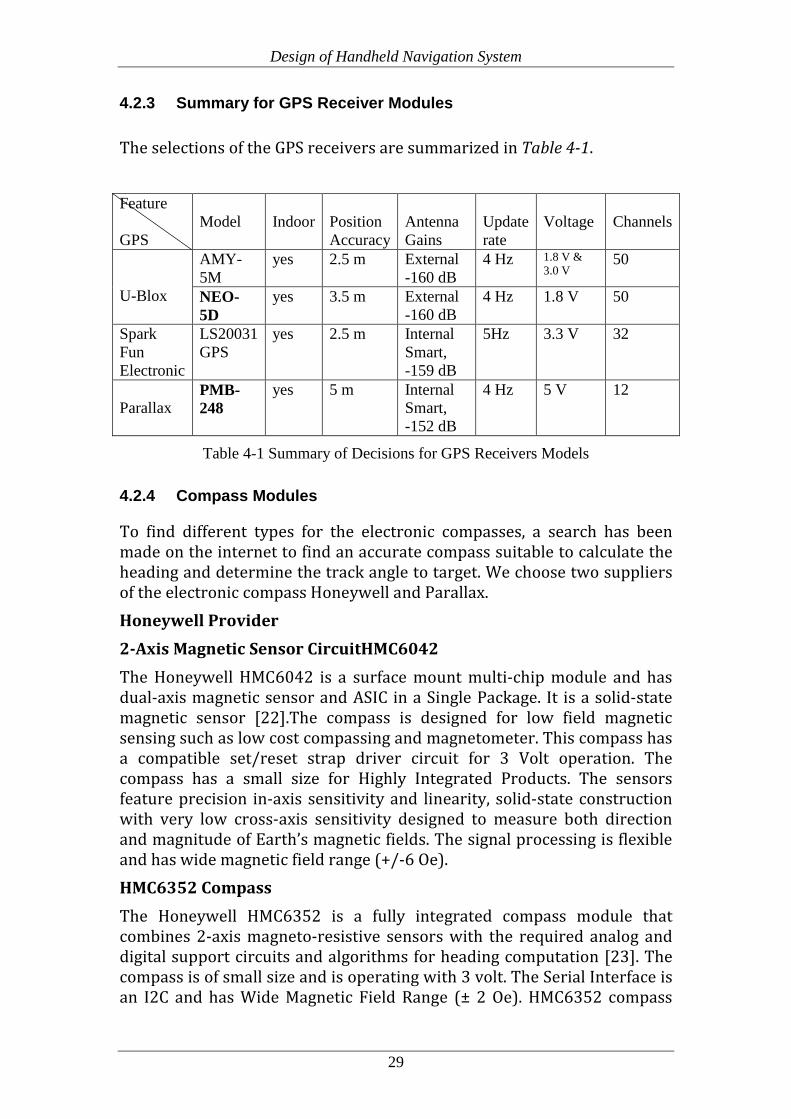
Design of Handheld Navigation System
4.2.3 Summary for GPS Receiver Modules
The selections of the GPS receivers are summarized in Table 4-1. Feature GPS
Model
Indoor
Position Accuracy
Antenna Gains
Update rate
Voltage
Channels
U-Blox
AMY-5M
yes 2.5 m External -160 dB
4 Hz 1.8 V & 3.0 V
50
NEO-5D
yes 3.5 m External -160 dB
4 Hz 1.8 V 50
Spark Fun Electronic
LS20031 GPS
yes 2.5 m Internal Smart, -159 dB
5Hz 3.3 V 32
Parallax
PMB-248
yes 5 m Internal Smart, -152 dB
4 Hz 5 V 12
Table 4-1 Summary of Decisions for GPS Receivers Models
4.2.4 Compass Modules
To find different types for the electronic compasses, a search has been made on the internet to find an accurate compass suitable to calculate the heading and determine the track angle to target. We choose two suppliers of the electronic compass Honeywell and Parallax. Honeywell Provider 2-Axis Magnetic Sensor CircuitHMC6042 The Honeywell HMC6042 is a surface mount multi-chip module and has dual-axis magnetic sensor and ASIC in a Single Package. It is a solid-state magnetic sensor [22].The compass is designed for low field magnetic sensing such as low cost compassing and magnetometer. This compass has a compatible set/reset strap driver circuit for 3 Volt operation. The compass has a small size for Highly Integrated Products. The sensors feature precision in-axis sensitivity and linearity, solid-state construction with very low cross-axis sensitivity designed to measure both direction and magnitude of Earth’s magnetic fields. The signal processing is flexible and has wide magnetic field range (+/-6 Oe). HMC6352 Compass The Honeywell HMC6352 is a fully integrated compass module that combines 2-axis magneto-resistive sensors with the required analog and digital support circuits and algorithms for heading computation [23]. The compass is of small size and is operating with 3 volt. The Serial Interface is an I2C and has Wide Magnetic Field Range (± 2 Oe). HMC6352 compass
29

Design of Handheld Navigation System
has a complete digital solution with heading output to Avoid Design of Hardware and compassing Firmware Routines. The compass has a good sensor can be used in strong magnetic field environment. Parallax supplier Hitachi HM55B Compass The Hitachi HM55B Compass module is dual axis magnetic field sensor to a sense of direction angle. The Compass should be capable of detecting micro-tesla (uT) variations in magnetic field strength. The compass has good facilities is easy to control and read. It has built-in resistor protection for data pins. An on-board regulator and resistor protection makes the 3 to 5 volt HM55B chip compatible with 5 volt and Built-in resistor protection for data pins which eliminates bus conflict risks. The compass is capable enough to read the direction in 30 to 40 milliseconds between start measurement and data-ready. The compass has integrated circuit and does not need to add any component to protect. The compass did not request time to calibration [23].
4.2.5 Selection of Compass
HMC6042 dual-Axis Magnetic Sensor Circuit The HMC6042 compass is small in size and the surface mounts multi chip. The compass has low cost and includes the state of 1042 series magneto-resistive sensors plus a precision mixed signal ASIC containing three Sensors Amplifiers. The HMC6042 is designed for low field magnetic sensing and it requires adding ADC when we want to Interface it to the Controller. Also, the compass requires two external SMT capacitors. Therefore, it has not been selected. HMC6352 Compass The Honeywell HMC6352 is a fully integrated compass module that combines dual-axis magneto-resistive sensors with the required analog and digital support circuits, and algorithms for heading computation. The compass is small in size and has a complete digital solution with heading output to avoid design of hardware and compassing firmware routines. The compass has a good sensor that can be used in strong magnetic field environments. It must be calibrated at least one time. The calibration window is recommended to be from 6 seconds up to 3 minutes. Therefore we did not choose this compass.
30

Design of Handheld Navigation System
Hitachi HM55B Compass The Hitachi HM55B Compass is small in size and has an integrated circuit. The compass module is dual axis magnetic field to a sense of direction and Built-in resistor protection for data pins. The compass can complete reading of the direction angle in 30 ms. the compass did not request time to calibrate. The compass should be capable of detecting micro-tesla (uT) variations in magnetic field strength. The compass has accurate reading for the direction angle (𝜃𝜃𝐶𝐶𝑐𝑐𝐶𝐶𝐶𝐶). Therefore we choose this compass for the project, see figure 4-2.
Figure 4-2 Hitachi HM55B Compass [24]
4.2.6 Summary for Compass Modules
The selections of the compass models are summarized in Table 4-2. Feature Compass
Model
Axes
Calibration
Start measurement
power
Pin connections
Honeywell
HMC6042 2 No request time
100 ms 3 V 20, complex
HMC6352 2 Up to 3min. 100 ms 3V 24, complex
Parallax Hitachi HM55B
2 No request time
30 ms 5 V 6, simple
Table 4-2 Summary of Decisions for Compass Models
4.2.7 Other Components
Microcontroller It has been decided to use Altera FPGA cyclone II (Field Programmable Gate Array) as a microcontroller in the design. The Cyclone II is of a low cost FPGA device family. The FPGA is an integrated circuit (ASIC) that can configure or be re-programmed on the circuit board. The designer can implement and prototype the design on FPGA more easily and quickly instead of manufacturing a new chip for the same design. Therefore, the design will be low in cost and can be developed in a short time. In addition, the FPGA has a higher quality since the documentation is better [24].
31

Design of Handheld Navigation System
HNS User Interface: LCD The LCD is one of the most important components in the design. The LCD helps the user of the handheld navigation to follow the direction to the target. The Nios-II processor is interfaced to the Optrex (16×2-character) LCD via Avalon bus to display the characters. Characters written to the LCD controllers are stored in an 80-column × 2-row buffer maintained via the driver [25]. Device drivers are provided in the HAL system library for the Nios-II processor. The result of the program carried out on Nios-II programs access the LCD controller as a character mode device using ANSI standard library routines, such as printf (). LCD is one of the peripherals which display the result of the software running on Nios-II processor. Implementing LCD controller in a FPGA provides the flexibility to incorporate additional LCD module features rapidly and easily. Therefore we use this LCD. SD Card To be able to draw the track between the start coordinate to the target, the HNS must save the values of GPS coordinators, Compass angle, and direction of the track to the target in the memory. One of these memories which is provided by Altera DE2 Education board is a secure data (SD card) memory. Secure Data (SD) card is an information storage device. The SD card is portable, which allows the data to be stored on it and to be transferred to other devices. Altera DE2 boards have an SD card port [26]. It allows an SD card to be connected to an FPGA based design on these boards, simplifying access to potentially large amounts of data. SD Card IP Core is a hardware circuit that enables the use of a SD card and Altera University Program (UP) supports it. SD Card IP Core provides an easy way to gain access data stored on a SD card device and the driver functions as a File Allocation Table (FAT) reader/writer version 16.Therefore we use this SD card. Battery The DE2 board power is 9 Volts, and to be able to use this board for a long time, required finding a rechargeable battery. It can work for a longer time than the normal battery. Then, we used a rechargeable battery 12 Volts/7.5Ah and that has required design in a small circuit to down convert the voltage to 9 volt. Figure 4-3 shows the design components for the down convertor.
32
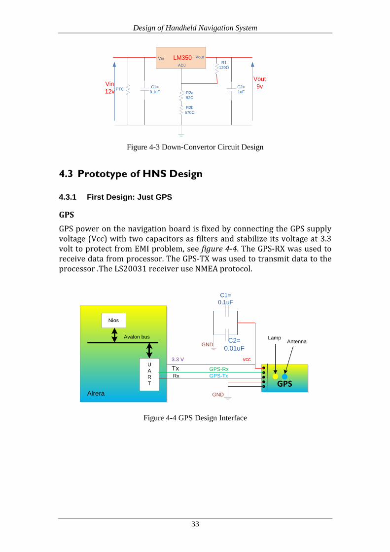
Design of Handheld Navigation System
LM350 Vout
Vin 12v
VinADJ R1
120Ω
C1= 0.1uF
C2= 1uFR2a
82Ω
R2b670Ω
Vout9vPTC
Figure 4-3 Down-Convertor Circuit Design
4.3 Prototype of HNS Design
4.3.1 First Design: Just GPS
GPS GPS power on the navigation board is fixed by connecting the GPS supply voltage (Vcc) with two capacitors as filters and stabilize its voltage at 3.3 volt to protect from EMI problem, see figure 4-4. The GPS-RX was used to receive data from processor. The GPS-TX was used to transmit data to the processor .The LS20031 receiver use NMEA protocol.
C1= 0.1uF
C2= 0.01uF
GPS
vcc3.3 V
GPS-Rx GPS-Tx
GND
GND
Nios
Alrera
UART
TxRx
Avalon busAntenna
Lamp
Figure 4-4 GPS Design Interface
33

Design of Handheld Navigation System
NMEA Protocol As mention in section 2.3.1.1 to National Marine Electronics Association, it is a standard protocol used by GPS receiver to transmit data. NMEA is configured to 57600 baud rate, 8 data bits, no parity and one stop bit. NMEA 0183 sentences are all ASCII. Each sentence begins with a dollar sign ($) and ends with a carriage return linefeed (<CR><LF>). GP is used to identify GPS data and the data is comma delimited. There are five NMEA sentences available, which can be used, GPGLL NMEA sentence in first design, GPRMC, GPGGA or GPGLL NMEA sentences can be used with second design, see table 4-3. NMEA output messages table. NMEA record Description
GGA Global positioning system fixed data
GLL Geographic position - latitude/longitude
GSA GNSS DOP and active satellites
GSV GNSS satellites in view
RMC Recommended minimum specific GNSS data
VTG Course over ground and ground speed
Table 4-3 NMEA Messages
UART Interface The Universal Asynchronous Receiver and Transmitter (UART) protocol was described in section 2.4. The UART is a serial communication protocol for the micro controller that is connected to the GPS receiver. UART TX is connected to GPS RX and UART RX is connected to GPS TX. First in First out (FIFO) FIFO is an acronym for First In First out, a method of processing and retrieving data. In a FIFO system, the first items entered are the first ones to be removed. In other words, the data are removed in the same order they are entered. FIFO is use commonly in electronic circuits for buffering and flow control, which is from hardware to software. First design calculation The goal of this design is to calculate the angle correction and draw route distance for the user of HN board via using the GPS receiver.
34

Design of Handheld Navigation System
4.3.2 Second Design: Using GPS and Compass
GPS Same as declaration in section 4.2.1 but from NMEA messages we can also use GPGGA NMEA sentences instead of using GPGLL NMEA sentence to delivers latitude and longitude coordinates. Compass The Hitachi HM55B compass module has a resistor protection which makes the 3 volt HM55B chip compatible with 5 volt in the design of compass IC. Therefore, it does not require adding any type of protection to the compass circuit and the compass connection are shown in figure 4-5.
Figure 4-5 Compass Design Interface
Compass connection There are two ways for connecting the compass to the microcontroller. The first one is by connecting the data input, and data output to the separate pin of microcontroller, as shown in figure 4-5. PIO As mentioned in section 2.6.1 The Parallel Input-Output core is standard interface for Nios-II and its general purpose, as shown in figure 4-5. The compass connection is via connecting the data input/output to the bidirectional pin of the interface of the microcontroller via PIO interface. Second Design Calculation The goal for the second design is to calculate the angle correction and draw route distance for the user of HN board via using the GPS receiver and compass.
Compass
Vcc
D I / O
D I DO
/ EN CLK 3 . 3 V
GND
Nios
Alrera
Avalon bus
DI / O
CLK
/ EN
PIO 3 . 3 V
35

Design of Handheld Navigation System
4.3.3 Switching Between the Designs
In this section, it will be explained how to switch between the Hardware and Software of the designs without requiring to stop the program and download the other Software. This design will give the user more flexibility to move in more freely in the implementation. In addition to abstract the program size, time and space in the memory (e.g. instead of create and download two program, we create one code for two design). The switch is used to switch between course over ground (GPS current position) and compass angle (current position). As shown in figure 4-6.
GPS/Compass
Currentangle
GPS
Compass angle
Course angle
Calculat Dist1 ,corse
Har.
coordinate
swtching=1=0
Figure 4-6 Switching Current Angle Design
4.3.4 Switch Connection Design
One of the good features of the DE2 board is its integrated design. There are 4 push-button switches and 18 toggle switches available on the Board, and these switches can be used for different purposes. By adding and define the HW as one "switchpio" in SOPC builder design and the SW create to be able to use this switch between the codes design.
36

Handheld Navigation System: Design and Implementation
5 Handheld Navigation System: Design and Implementation In this chapter, the specific work for the system will be presented while the whole system is divided into three blocks from their diverse function. The implementation environment, both the hardware and software, will be introduced as well as the related information. Then the key steps of the designs are verified and are combined with some testing functions. In brief, a design technical view for the system is presented to reach the research aim.
5.1 System Description System Overview This section will give a review of the Handheld Navigation System design. The developed system consists of models on the Handheld Navigation board, DE2 board and Remote section (Application development). The architecture of the design is shown in figure 5-1.
CPU(Nios)
JATG UART
INT RAM
SRAM
EXP.
Hea
der G
PIO
-0 (2
*20 )
Compass
GPS
Dow
ncon
vert
or
Circ
uit
EXP.
Hea
der (
2*20
)
LCD
SD-card
PI/O
UART
FPGA
USB blaster i
PC
Lamp Antenna
HN board (PCB)
Inpu
tO
utpu
t
Aplication program(NiosII SW)
In/OutGUI
Embedded SystemDE2
Remote section
12v DC
9v
Figure 5-1 System Design Organization
The Handheld navigation board consists of LS20031 GPS receiver, HM55B Hitachi compass IC, down convertor circuit and expansion headers (2*20) to connect the models to an FPGA. The HN system design is depicted in figure 5-1. Furthermore, a down-convertor circuit is design to down-convert 12 Volts DC supply voltage to 9 Volts DC to be used for the DE2 board, instead of using the AC supply. The chargeable battery gives flexibility to the user to move with the HN system. For real hardware implementation a DE2 development board is used. We
37

Handheld Navigation System: Design and Implementation
implemented our design by using the features of the DE2 board. The components that we used are SD card, LCD display and the on board SRAM. The SD card is used for saving data from the experiments. To communicate between the DE2 board and the PC, an USB blaster cable is used.
5.1.1 Navigation Board
As described in section 2.6.1, the HN system parts as depicted in figure 5-1. The DE2 board is used for prototyping. Quartus-II software is used with DE2 bard to design a system in SOPC builder in Quartus using the soft-core of Nios-II processor.
5.1.2 Remote Section: Offline Application Development
The NIOS-II development environment is used to develop the Application-programming interface (API) between GPS, Compass and PC for reading and analyzing the data. The USB blaster is used for communication between PC and the DE2 board. Further the developed Nios II system will send and receive data from the external devices via UART and PIOs. Nios II soft-core can send and receive 32-bits of data at a time. Nios II Integrated Development Environment (IDE) is used to run the software for the Nios II processor. The developed API for the HN system in Nios II (IDE) can be used for Nios after creating the system for Nios II processor in Quartus using SOPC builder.
5.2 Navigation Board Design This section explains the hardware mechanisms for the two designs as mentioned in section 5.1.2. In addition, it describes the circuit board components and how it is fixed.
5.2.1 Functionality of the Board
All hardware components are tested individually to verify that they are working correctly, see figure 5-2. The developed program controls all the necessary hardware components for the proper operation of the designed system. The functionality of the HN board is used to calculate the relative direction. GPS Receiver As mentioned in section 4.1.1, the LS20031 GPS function is used to receive the GPS satellites messages. Then usage the coordinate points of the track to calculate the relative direction, course over ground and distance.
38

Handheld Navigation System: Design and Implementation
Electronic Compass Function As mentioned in section 4.1.2, the HM55B Compass is used to calculate the current angle of the user movement direction. Power Supply The power supply used for the DE2 board is 9 Volts DC. The re-chargeable DC battery available was 12Volts and 1.5 Ah. Therefore, we designed a down converter circuit to provide the development board with 9 volts. The internal supply voltages for DE2 board are 3.3V, 2.5V and 1.8V.
5.2.2 Components and PCB Implementation
The purpose of this section is to explain the main components of the Handheld Navigation system, down converter circuit and the of printed circuit board (PCB), see figure 5-2.
HMB55 Hitachi Compass
LS20031GPS Receiver
Expansion Header 2*20
Down Convertor Circuit
Figure 5-2 Handheld Navigation PCB Board
GPS
As described in section 4.1.1, the LS20031 GPS receiver is used. Compass
The HM55B Hitachi compass is used, as mentioned in section 4.1.2. Down Converter Design
As mentioned in previous section it is required to design an electronic circuit to be able to down convert the available DC power supply to 9 volts. The down converter circuit consists of TM335 IC, two capacitors, two connectors (2 pole) and three resistors. Moreover, a positive temperature
39

Handheld Navigation System: Design and Implementation
coefficient PTC resistor was added as protection for the down convertor circuit from increasing energy of the battery. The re-chargeable battery gives the user longer time to move with the Handheld Navigation system. PCB Board
The Printed Circuit Board (PCB) is designed with the EAGLE PCB program. The GPS and Compass are mounted together on the PCB board for a good connection and it is also feasible to move with the board safely. The schematic of the HNS system designed circuit is shown in figure 9-1, figure 9-2. The Handheld Navigation PCB board consists of two parts, LS20031 GPS receiver and Hitachi HM55B compass and expansion header (2*20). The second part is consisting of down convertor circuit, as shown in figure 5-2.
5.2.3 Interfaces to DE2 Board
In this section will explain the interface signals and interface protocol for the GPS receiver module and the compass module: Interface Signals
Figure 5-3 shows the connections between Nios-II core, GPS receiver and compass. The functionality of the GPS receiver and compass are described in Section 4.1.1 and 4.1.2. The details of each interface are discussed in the following subsections.
GPS
CompassNios II(CPU)
Aval
on-B
us
UART TX
UART RX
PIO
PIO
PIO
GPS TX
GPS RX
DI/O
CLK
/EN
Figure 5-3 Block Diagram of Design Communication
40
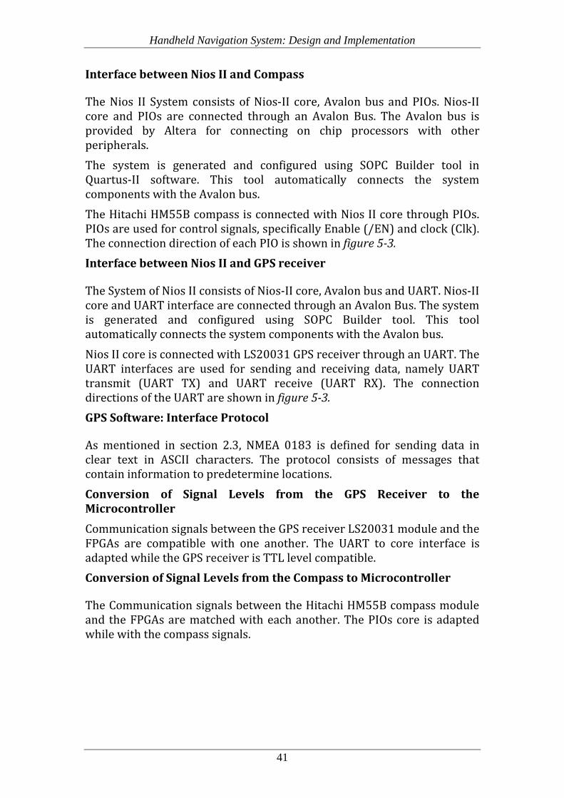
Handheld Navigation System: Design and Implementation
Interface between Nios II and Compass
The Nios II System consists of Nios-II core, Avalon bus and PIOs. Nios-II core and PIOs are connected through an Avalon Bus. The Avalon bus is provided by Altera for connecting on chip processors with other peripherals. The system is generated and configured using SOPC Builder tool in Quartus-II software. This tool automatically connects the system components with the Avalon bus. The Hitachi HM55B compass is connected with Nios II core through PIOs. PIOs are used for control signals, specifically Enable (/EN) and clock (Clk). The connection direction of each PIO is shown in figure 5-3. Interface between Nios II and GPS receiver
The System of Nios II consists of Nios-II core, Avalon bus and UART. Nios-II core and UART interface are connected through an Avalon Bus. The system is generated and configured using SOPC Builder tool. This tool automatically connects the system components with the Avalon bus. Nios II core is connected with LS20031 GPS receiver through an UART. The UART interfaces are used for sending and receiving data, namely UART transmit (UART TX) and UART receive (UART RX). The connection directions of the UART are shown in figure 5-3. GPS Software: Interface Protocol
As mentioned in section 2.3, NMEA 0183 is defined for sending data in clear text in ASCII characters. The protocol consists of messages that contain information to predetermine locations. Conversion of Signal Levels from the GPS Receiver to the Microcontroller Communication signals between the GPS receiver LS20031 module and the FPGAs are compatible with one another. The UART to core interface is adapted while the GPS receiver is TTL level compatible. Conversion of Signal Levels from the Compass to Microcontroller
The Communication signals between the Hitachi HM55B compass module and the FPGAs are matched with each another. The PIOs core is adapted while with the compass signals.
41

Handheld Navigation System: Design and Implementation
5.3 Application Software Development
In this section, we will describe how the software prototypes are designed. We design two prototypes of SW; the first design consists of GPS calculation code on the Nios II processor. The second program consists of GPS and Compass software code on the processor.
5.3.1 Methodology
In this section the development of the software for two kinds of designs is described. The first is development of code for UART communication with GPS receiver and for direction calculations from GPS coordinates. The second design consists of the first program and in addition programs for handling an HM55B Hitachi compass and corresponding direction calculations. Moreover, the software is written in ANSI C and compiled with Nios-II C2H Compiler.
5.3.2 Using GPS Alone
The first assignment in the project is to calculate distance and direction corrections with the micro controller that communicates with the GPS via a UART serial communication link. Only the GPS position and actual course direction information is available. The GPS receiver must be moved in order to calculate the course direction from coordinates from several position points. LS20031 GPS receiver
To calculate the navigation direction between two points in the first prototype design, the GPS receiver is configured to transmit the GPGLL coordinates from one to five times per second. We are using one message per second. The GPGLL message contains the calculated coordinates based on received GPS signals from a number of satellites. When the microcontroller receives a GPGLL message, it saves only the required data. In the beginning, it checks if it is the correct data by controlling the characters. It should start with the character $ followed by GPGLL. The received data includes a fixed number of digit fields and commas and it is therefore possible to extract the data by counting the commas ",". The checksum ‘*’ and <CR><LF> are received at the end of the message as mentioned in section 2.3. 8 digits describe the latitude and 9 digits describe the longitude. The Course over ground can be 1 to 3 characters i.e., 0 to 360 degrees.
42

Handheld Navigation System: Design and Implementation
Conversion of coordinates
The coordinates, data attained from the GPS receiver, are in WGS84 format. This format has an integer number for degrees and a decimal number for minutes. In order to calculate the coordinates they must be transformed into coordinates in decimal degrees format. Calculation of Distance, Direction and Course over Ground
The Harversine formula that is presented in section 2.6 can be implemented to calculate the points on a spherical plan. Calculate Distance
The coordinates from the GPS receiver are converted to decimal degrees and then converted to radians. Then the microcontroller uses this radian coordinates to calculate the distance from current position to the destination position. As explained in the formula below and also mention in section 2.8.
𝒍𝒍𝒍𝒍𝒍𝒍𝐥𝐥 = 𝒍𝒍𝒍𝒍𝐥𝐥 × 𝑪𝑪𝒔𝒔𝐥𝐥𝟏𝟏𝟔𝟔
(5-1)
𝒍𝒍𝒄𝒄𝒕𝒕𝐥𝐥 = 𝒍𝒍𝒄𝒄𝐥𝐥 × 𝑪𝑪𝒔𝒔𝐥𝐥𝟏𝟏𝟔𝟔
(5-2)
𝒍𝒍𝒍𝒍𝒍𝒍𝐥𝐥 = 𝒍𝒍𝒍𝒍𝐥𝐥 × 𝑪𝑪𝒔𝒔𝐥𝐥𝟏𝟏𝟔𝟔
(5-3)
𝒍𝒍𝒄𝒄𝒕𝒕𝐥𝐥 = 𝒍𝒍𝒄𝒄𝐥𝐥 × 𝑪𝑪𝒔𝒔𝐥𝐥𝟏𝟏𝟔𝟔
(5-4)
∆𝒍𝒍𝒍𝒍𝒍𝒍 = 𝒍𝒍𝒍𝒍𝒍𝒍𝐥𝐥 − 𝒍𝒍𝒍𝒍𝒍𝒍𝐥𝐥 (5-5) ∆𝒍𝒍𝒄𝒄𝒕𝒕𝒈𝒈 = 𝒍𝒍𝒄𝒄𝒕𝒕𝒈𝒈𝐥𝐥 − 𝒍𝒍𝒄𝒄𝒕𝒕𝒈𝒈𝐥𝐥 (5-6)
𝒍𝒍 = 𝒔𝒔𝒔𝒔𝒕𝒕 𝐥𝐥 ∆𝒍𝒍𝒍𝒍𝒍𝒍𝐥𝐥 + 𝒄𝒄𝒄𝒄𝒔𝒔(𝒍𝒍𝒍𝒍𝒍𝒍𝐥𝐥) × 𝒄𝒄𝒄𝒄𝒔𝒔(𝒍𝒍𝒍𝒍𝒍𝒍𝐥𝐥) × 𝒔𝒔𝒔𝒔𝒕𝒕𝐥𝐥 ∆𝒍𝒍𝒄𝒄𝒕𝒕𝒈𝒈
𝐥𝐥 (5-7)
𝒄𝒄 = 𝐥𝐥 × 𝒍𝒍𝒍𝒍𝒍𝒍𝒕𝒕𝐥𝐥(√𝒍𝒍,𝐥𝐥 − 𝒍𝒍) (5-8)
𝒅𝒅 = 𝑹𝑹 × 𝒄𝒄 (5-9)
43
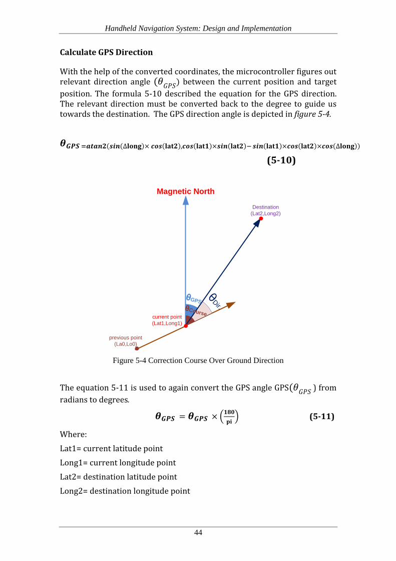
Handheld Navigation System: Design and Implementation
Calculate GPS Direction
With the help of the converted coordinates, the microcontroller figures out relevant direction angle (𝜃𝜃𝐺𝐺𝐺𝐺𝐺𝐺) between the current position and target position. The formula 5-10 described the equation for the GPS direction. The relevant direction must be converted back to the degree to guide us towards the destination. The GPS direction angle is depicted in figure 5-4.
𝜽𝜽𝑮𝑮𝑮𝑮𝑮𝑮 =𝒍𝒍𝒍𝒍𝒍𝒍𝒕𝒕𝐥𝐥(𝒔𝒔𝒔𝒔𝒕𝒕(∆𝐥𝐥𝐨𝐨𝐝𝐝𝐥𝐥)× 𝒄𝒄𝒄𝒄𝒔𝒔(𝐥𝐥𝐝𝐝𝐝𝐝𝐥𝐥),𝒄𝒄𝒄𝒄𝒔𝒔(𝐥𝐥𝐝𝐝𝐝𝐝𝐥𝐥)×𝒔𝒔𝒔𝒔𝒕𝒕(𝐥𝐥𝐝𝐝𝐝𝐝𝐥𝐥)−𝒔𝒔𝒔𝒔𝒕𝒕(𝐥𝐥𝐝𝐝𝐝𝐝𝐥𝐥)×𝒄𝒄𝒄𝒄𝒔𝒔(𝐥𝐥𝐝𝐝𝐝𝐝𝐥𝐥)×𝒄𝒄𝒄𝒄𝒔𝒔(∆𝐥𝐥𝐨𝐨𝐝𝐝𝐥𝐥))
(5-10)
Magnetic North
Destination (Lat2,Long2)
current point (Lat1,Long1)
θDir. θCourse
θGPS
previous point (La0,Lo0)
Figure 5-4 Correction Course Over Ground Direction
The equation 5-11 is used to again convert the GPS angle GPS(𝜃𝜃𝐺𝐺𝐺𝐺𝐺𝐺 ) from radians to degrees.
𝜽𝜽𝑮𝑮𝑮𝑮𝑮𝑮 = 𝜽𝜽𝑮𝑮𝑮𝑮𝑮𝑮 × 𝐥𝐥𝟏𝟏𝟔𝟔𝐬𝐬𝐝𝐝 (5-11)
Where: Lat1= current latitude point Long1= current longitude point Lat2= destination latitude point Long2= destination longitude point
44

Handheld Navigation System: Design and Implementation
Calculate Course over ground
From the GPS receiver coordinates, we calculate the course over ground angle every second between previous position and the current position using FIFO buffer, as shown in figure 5-3. We use the 1st and 5th coordinate of the FIFO. The microcontroller is used to calculate the course angle(𝜽𝜽𝒄𝒄𝒄𝒄𝒄𝒄𝒄𝒄) that represents the current angle of the HNS, see formula 5-22. In addition, the direction must be converted to the degree units.
𝐥𝐥𝐝𝐝𝟔𝟔 = 𝐥𝐥𝐝𝐝𝟔𝟔 × 𝐬𝐬𝐝𝐝𝐥𝐥𝟏𝟏𝟔𝟔
(5-13)
𝐥𝐥𝐨𝐨𝟔𝟔 = 𝐥𝐥𝐨𝐨𝟔𝟔 × 𝐬𝐬𝐝𝐝𝐥𝐥𝟏𝟏𝟔𝟔
(5-14)
𝐥𝐥𝐝𝐝𝐥𝐥 = 𝐥𝐥𝐝𝐝𝐥𝐥 × 𝐬𝐬𝐝𝐝𝐥𝐥𝟏𝟏𝟔𝟔
(5-15)
𝐥𝐥𝐨𝐨𝐥𝐥 = 𝐥𝐥𝐨𝐨𝐥𝐥 × 𝐬𝐬𝐝𝐝𝐥𝐥𝟏𝟏𝟔𝟔
(5-16)
∆𝐥𝐥𝐝𝐝 = 𝐥𝐥𝐝𝐝𝐥𝐥 − 𝐥𝐥𝐝𝐝𝟔𝟔 (5-17) ∆𝐥𝐥𝐨𝐨 = 𝐥𝐥𝐨𝐨𝐥𝐥 − 𝐥𝐥𝐨𝐨𝟔𝟔 (5-18)
𝐝𝐝 = 𝐝𝐝𝐝𝐝𝐝𝐝 𝐥𝐥 ∆𝐥𝐥𝐝𝐝𝐥𝐥 + 𝐝𝐝𝐨𝐨𝐝𝐝(𝐥𝐥𝐝𝐝𝟔𝟔) × 𝐝𝐝𝐨𝐨𝐝𝐝(𝐥𝐥𝐝𝐝𝐥𝐥) × 𝐝𝐝𝐝𝐝𝐝𝐝𝐥𝐥 ∆𝐥𝐥𝐨𝐨
𝐥𝐥 (5-19)
𝐝𝐝 = 𝐥𝐥 × 𝐝𝐝𝐝𝐝𝐝𝐝𝐝𝐝𝐥𝐥(√𝐝𝐝,𝐥𝐥 − 𝐝𝐝) (5-20)
𝐝𝐝 = 𝐑𝐑 × 𝐝𝐝 (5-21) The direction angle (𝜃𝜃𝑑𝑑𝑑𝑑𝑑𝑑1) can be calculated by subtracting the course angle from the GPS direction, using equation 5-24. The direction (𝜃𝜃𝑑𝑑𝑑𝑑𝑑𝑑1) can guide the user of Handheld Navigation System from current position to the destination, as shown in figure 5-3.
𝜽𝜽𝒄𝒄𝒄𝒄𝒄𝒄𝒄𝒄 =𝒍𝒍𝒍𝒍𝒍𝒍𝒕𝒕𝐥𝐥(𝒔𝒔𝒔𝒔𝒕𝒕(∆𝐥𝐥𝐨𝐨)× 𝒄𝒄𝒄𝒄𝒔𝒔(𝐥𝐥𝐝𝐝𝐥𝐥),𝒄𝒄𝒄𝒄𝒔𝒔(𝐥𝐥𝐝𝐝𝟔𝟔)×𝒔𝒔𝒔𝒔𝒕𝒕(𝐥𝐥𝐝𝐝𝐥𝐥)−𝒔𝒔𝒔𝒔𝒕𝒕(𝐥𝐥𝐝𝐝𝟔𝟔)×𝒄𝒄𝒄𝒄𝒔𝒔(𝐥𝐥𝐝𝐝𝐥𝐥)×𝒄𝒄𝒄𝒄𝒔𝒔(∆𝐥𝐥𝐨𝐨)) (5-22)
Where: La0= previous latitude point Lo0= previous longitude point
𝜽𝜽𝒄𝒄𝒄𝒄𝒄𝒄𝒄𝒄 = 𝜽𝜽𝒄𝒄𝒄𝒄𝒄𝒄𝒄𝒄 × 𝐥𝐥𝟏𝟏𝟔𝟔𝑪𝑪𝒔𝒔 (5-22)
𝜽𝜽𝒅𝒅𝒔𝒔𝒄𝒄𝐥𝐥 = 𝜽𝜽𝑮𝑮𝑮𝑮𝑮𝑮 –𝜽𝜽𝒄𝒄𝒄𝒄𝒄𝒄𝒄𝒄 (5-23)
45

Handheld Navigation System: Design and Implementation
HNS and Destination
There are varieties of factors that have an effect on the GPS receiver signal such as weather, ionosphere layer etc. Due to these reasons it is difficult for the GPS receiver to receive accurate data, to be able to calculate the precise distance and direction. The program algorithm will check the direction correction of the handheld navigator. Either the user goes towards right or left of the straight direction to the target. There are two methods to know if the user is close to the destination position or not. First is by checking the current coordinates with the destination coordinates. And second by calculating the distance if the user is near to the destination in 5 meters then it meets the target. Control the Right Direction
The direction correction is measured to control the user HNS device. The course over ground is designated by "𝜽𝜽𝒄𝒄𝒄𝒄𝒄𝒄𝒄𝒄 " and the direction of the GPS receiver is”𝜽𝜽𝑮𝑮𝑮𝑮𝑮𝑮 ". The desired direction correction for the HNS is"𝜽𝜽𝒅𝒅𝒔𝒔𝒄𝒄𝐥𝐥”. This direction angle "𝜃𝜃𝑑𝑑𝑑𝑑𝑑𝑑1" is calculated by using the formula in section 5.2.3. The block diagram is shown in figure 5-5. The control direction correction signal is calculated by:
𝜽𝜽𝒅𝒅𝒔𝒔𝒄𝒄𝐥𝐥 = 𝜽𝜽𝑮𝑮𝑮𝑮𝑮𝑮 - 𝜽𝜽𝒄𝒄𝒄𝒄𝒄𝒄𝒄𝒄
GPS
+
Calculat direction
Harv.
SystemUser
Current Position,Θdir1. Position,
θdir.1
Dest. (La2,Lo2) Current position(La1,Lo1)
θwant
Current Position,Θdir1.
+
‒
SD-card,LCD Disply
Calculat Current
directionHarv.
θCourse
Figure 5-5 Block Diagram of Direction Correction
Description of the program
The program algorithm is shortly described. First the program calculates the distance and direction correction from the receiver coordinates.
46

Handheld Navigation System: Design and Implementation
Then the Handheld Navigation System is controlled automatically by the microcontroller. Figure 5-6 describes the GPS control design flow chart. The HNS takes information from the GPS receiver. The microcontroller uses this data to calculate the distance, relative direction and course over ground. The program will update calculated values every second and displays the results on LCD and stores data on a SD card.
SturtupGPS
Corrdinates,Distance & Direction
SD-card,LCD
Microcontroller
Start
Figure 5-6 GPS Control Design Flowchart
Mechanism of program work
In this section, we will describe how the software works and describes a feature of the program. Start-up
In the start-up step the microcontroller initializes all the devices and loads the initial values for current position. Control
The control feature controls how the Handheld Navigation System calculates distance and direction correction. Figure 5-7 shows the GPS receiver flowchart and direction correction.
47

Handheld Navigation System: Design and Implementation
Calculate distance, Course and direction
If near destination <5m
Calculate distance, Course and direction(Harversin Formula)
Start
Receive GPGLL coordinats
Latitude, Longitude
Convert Latitude, Longitude to dicemal &
radius
SD-card,Display
Corrdinates,direction
yes
No
Convert Course and direction to degree
Control the correction direction(straight, left, right )
Convert Course and direction to degree
Figure 5-7 Block Diagram for GPGLL Message
First the GPS receiver receives the GPGLL coordinates for the current position and converts them to decimal degrees. Then it converts the coordinates to radians. The Harversine formula is used to calculate the distance, direction and course over ground. Again the result is converted to degrees. Then the program will check if we are near the destination point within 5 meters. If the destination is so close then the program jumps to the start state and waits for new coordinates. Otherwise it jumps to the next step and calculates the new distance, course and direction. And again converts it to degrees. In the next state it controls the user correction direction and displays the final result on the LCD display and saves the data on the SD-card.
48

Handheld Navigation System: Design and Implementation
5.3.3 Using GPS Receiver and Compass
The second part of the project is to calculate the distance, relative direction, current direction and direction correction using the GPS receiver and the compass. The microcontroller will communicate with GPS and compass through the UART and I/O interfaces. The USB blaster cable is used for communication between the DE2 board and the host PC. The UART serial communication interface is described in section 2.6.1. The PIO is a parallel communication port that has 32 bits as mentioned in section 2.6.1. LS20031 GPS and Hitachi HM55B Compass
The LS20031 GPS receiver has been described in section 5.2.2. The GPS coordinates are used to calculate the relevant direction angle (𝜽𝜽𝑮𝑮𝑮𝑮𝑮𝑮 ) and distance. This section describes the operation of the compass and how to calculate the current direction angle (𝜽𝜽𝑪𝑪𝒄𝒄𝑪𝑪𝑪𝑪) of the HNS.
Conversion of Coordinates and Angel
The GPS coordinate conversions are mentioned in section 5.3.2. The data transmitted and received from the compass is in the form of the most significant bit (MSB) first. The compass angle value can be in negative or positive, depending on the direction of the compass relative to the magnetic north. To convert the negative angle value to positive we should add 360 degree to the compass angle. The HM55B compass functionality can be divided into different parts such as set/reset operation, magnetic sensor data acquisition and heading computation. The table 5-1 describes the commands which can be used for the operation of the compass.
Binary Value Quantity
0000 Reset device
1000 Start measurement
1100 Report measurement status (and transmit the measurement if it's ready)
Table 5-1 Compass Commands
49

Handheld Navigation System: Design and Implementation
Calculation of direction
In section 5.3.2.2 it has been described how the microcontroller can be used to calculate the GPS relative direction. The compass can be used to compute the current angle(𝛉𝛉𝐂𝐂𝐨𝐨𝐭𝐭𝐬𝐬). The compass calculates the current direction through two sensors by reading the x and y magnetic field strength measurements (N cosθ, N sinθ). By using trigonometric identities the angle (θ) “arctangent y/x” can be calculated. The trigonometric identities are shown in the figure 5-8 and formulas below.
N
EW
S
θ
θ
x= N cosθ
y = N sinθ
Figure 5-8 Arctangent of Compass Angle
The direction correction of the Handheld Navigation System can be calculated by subtracting the compass angle (𝜽𝜽𝑪𝑪𝒄𝒄𝑪𝑪𝑪𝑪) from the GPS relevant direction(𝜽𝜽𝑮𝑮𝑮𝑮𝑮𝑮) . The direction correction (𝜽𝜽𝒅𝒅𝒔𝒔𝒄𝒄𝐥𝐥 ) computation is shown in equation 5-28. The direction correction is shown in figure 5-9.
𝐱𝐱 = 𝐍𝐍𝐝𝐝𝐨𝐨𝐝𝐝 𝛉𝛉 (5-24) 𝐲𝐲 = 𝐍𝐍 𝐝𝐝𝐝𝐝𝐝𝐝𝛉𝛉 (5-25)
𝐝𝐝𝐝𝐝𝐝𝐝 𝛉𝛉 = 𝐍𝐍𝐝𝐝𝐝𝐝𝐝𝐝𝛉𝛉𝐍𝐍 𝐝𝐝𝐨𝐨𝐝𝐝𝛉𝛉
= 𝐲𝐲𝐱𝐱 (5-26)
𝜽𝜽𝑪𝑪𝒄𝒄𝑪𝑪𝑪𝑪 = 𝐝𝐝𝐝𝐝𝐝𝐝−𝐥𝐥 −𝒚𝒚𝒙𝒙 (5-27)
𝜽𝜽𝒅𝒅𝒔𝒔𝒄𝒄𝐥𝐥 = 𝜽𝜽𝑮𝑮𝑮𝑮𝑮𝑮𝑮𝑮 − 𝜽𝜽𝑪𝑪𝒄𝒄𝑪𝑪𝑪𝑪 (5-28)
50

Handheld Navigation System: Design and Implementation
Magnetic North
Destination (Lat2,Long2)
Current point (Lat1,Long1)
θDir. θComp.
θGPS
Figure 5-9 Second Design Direction Correction Vector
Control the Right Direction
The direction correction is computed to control the HNS. The compass current angle is designated by "𝜽𝜽𝒄𝒄𝒄𝒄𝑪𝑪𝑪𝑪 " and the direction to the destination based on the GPS receiver coordinates is "𝜽𝜽𝑮𝑮𝑮𝑮𝑮𝑮 ". The desired direction correction for the HNS user is"𝜽𝜽𝒅𝒅𝒔𝒔𝒄𝒄𝐥𝐥”. This direction angle "𝜽𝜽𝒅𝒅𝒔𝒔𝒄𝒄𝐥𝐥" is calculated by using the formula in section 5.2.3. The block diagram shows in figure 5-10. The control of direction correction signal is calculated by:
𝜽𝜽𝒅𝒅𝒔𝒔𝒄𝒄𝐥𝐥 = 𝜽𝜽𝑮𝑮𝑮𝑮𝑮𝑮 -𝜽𝜽𝒄𝒄𝒄𝒄𝑪𝑪𝑪𝑪
GPS/Compass
+
Calculat direction
SystemUser
Current Position,Θdir2. Position,θdir2
Dest. (La2,Lo2) Current position(La1,Lo1)
θwant
Current Position,Θdir2.
+
θComp.‒
SD-card,LCD Disply
Figure 5-10 Direction Block Diagram
51

Handheld Navigation System: Design and Implementation
Description of GPS and Compass program
The program algorithm is shortly described. First the program calculates the distance and relative direction(𝜽𝜽𝑮𝑮𝑮𝑮𝑮𝑮) from the GPS receiver coordinates. The current direction is calculated from the compass data. Then the Handheld Navigation System is controlled automatically by the microcontroller. Figure 5-11 can defines the GPS-Compass control design flowchart. The microcontroller takes information from the GPS-Compass. The microcontroller uses this data to calculate the distance, relative direction and current direction. The program will update the calculated values every second and displays the results on LCD and stores data on a SD-card.
procesor
SturtupGPS+Compass
LCD,SD-card
Corrdinates,Distance & Direction
Coodinates+
Angle
Start
Figure 5-11 GPS and Compass Control System Flowchart
Mechanism of programs work
In this section, we will describe how the program works and explain the features of the software. Start up
In the start-up step the microcontroller initializes all the devices and loads the initial values for current location and current angle. Control
The control feature controls how the Handheld Navigation System calculates distance, relative direction, current direction and direction
52

Handheld Navigation System: Design and Implementation
correction. Figure 5-12 shows the GPS-Comp flowchart and direction correction.
Start
X and Y-direction alignment
If angle < 0 , angle += 360Else angle > 360, angle -= 360
Calculate Θ = 〖tan〗^(-1) (y/x)
Gps dir.
SD card,LCD-Display
direction Correction= GPS dir.- angle
Coordinates,direction
Reading the data(x&y)axis
Output value Update after 100 msec
Figure 5-12 Direction from Compass-GPS flow
The GPS receiver control program is described in section 5.2.2. The compass starts reading the earth magnetic sensors after 40 ms. From the measured axis (x, y) the program calculates the current angle through the arctangent y/x formula. In the next step the algorithm checks if the angle is negative and then adds 360 degrees otherwise does nothing. The output of the compass is always updated after 100ms. The main program will compute the direction correction (𝛉𝛉𝐝𝐝𝐝𝐝𝐭𝐭𝐥𝐥) by subtracting the compass current angle (𝛉𝛉𝐂𝐂𝐨𝐨𝐭𝐭𝐬𝐬) from the GPS relative direction(𝜽𝜽𝑮𝑮𝑮𝑮𝑮𝑮).
In the last state it controls the HNS direction correction and displays the final result on the LCD display and saves the data on the SD-card.
53
Handheld Navigation System: Design and Implementation
5.3.4 Switching between the two Applications
Switching between GPS only and GPS-Compass
The “GPS only design” and the “GPS-Compass” design are described in the previous sections. These two designs need two separate programs to run on the FPGA board. But the FPGA can run one program at one time. To load one program for execution and then remove it and load the other program is time consuming. To solve this problem we used a switch between two programs. Both programs are loaded together and we can switch between them through the switch. Control the Right Direction
As mentioned in the section 5.3.2 and 5.3.3, the direction correction is used to control the HNS. The current direction"𝜽𝜽𝒄𝒄𝒄𝒄𝒄𝒄𝒄𝒄." or "𝜽𝜽𝒄𝒄𝒄𝒄𝑪𝑪𝑪𝑪." can be selected. One of these angles together with the destination direction from the GPS coordinates is used to calculate the direction correction. The diagram of the “switchpio” is depicted in figure 5-13.
GPS/Compass
+
Calculat direction
Har.
SystemUser
Position,Distance,θdir Position,Distance,θdir
Dest. (La2,Lo2) Current position(La1,Lo1)
Distance, θwant
Current Position, Distance, Θdir.
θCurrent‒ +
GPS
Compass angle
Course angle
SD-card,Disply
Calculat Dist1 ,corse
Har.
coordinate
swtching
Figure 5-13 Switching Direction Block Diagram
Description for GPS and Compass programs Switching
The general description of the GPS and GPS-Compass programs are described in the previous sections. The switching procedure switches between the course over ground "𝜽𝜽𝒄𝒄𝒄𝒄𝒄𝒄𝒄𝒄." and the compass angle "𝜽𝜽𝒄𝒄𝒄𝒄𝑪𝑪𝑪𝑪."
The Handheld Navigation is controlled automatically by the
54

Handheld Navigation System: Design and Implementation
microcontroller to calculate the right direction. The switching control between two programs is shown in the figure 5-14.
Choos programs
Program 2 GPS&Compass
Program 2Program 1
Program GPS1
Start
Figure 5-14 Switching Designs System Flowcharts
Mechanism of programs work
Control
In the first step the GPS and compass are initialized. The “switchpio” is used to switch between two programs design, if the switch position is 1 the GPS alone program path in selected and if the switch position is 0 the GPS-Compass combination program path is selected. The final results are displayed on the LCD and store on SD-Card according the below figure 5-15.
Start
Choose program
Program2 GPS&Compass
Program1 GPS
Program 1 Program 2
LCD & SD-card
Corrdinates,Distance & Direction
Figure 5-15 Display and Save Designs Result
55
Prototyping,Testing and Results
6 Prototyping, Testing & Results 6.1 Prototyping HNS Platform
6.1.1 Hardware Organization
The essential components that build up the co-designed HW-SW are Nios II, UART, PIO, SD-Card and LCD are depicted in figure 6-1.
GPSCompass
HN Board
Nios II\e Int. RAM
JTAG UART SRAM
PIOs UART
JTAG
SD-Card LCD
Avalon-BusAvalon-BusAvalon-Bus
USB Blaster Cable
DE2 Board
Handheld Navigation System Board
Figure 6-1 Hardware Structural Design
The figure above shows the interface between the GPS and Compass components and Nios II. SRAM (Static Random Access Memory) is used to store the program of Nios II core. The JTAG UART (Joint Test Access Group Universal Asynchronous Receiver Transmitter) is used for the communication with the host PC. The compass that is interfaced with Nios II core sends and receives the data through Parallel IOs, the GPS sends and receives the data through an UART interface. The LCD is used to display the test results, and the SD-card is used to save the test data.
56

Prototyping,Testing and Results
6.1.2 Configuration of First Design and Integration
As mentioned in section 5.2.2.4, the design is configured in System-on-Programmable-Chip (SOPC) Builder. SOPC is a development tool and it is part of the Quartus-II software. The design flow begins by creating a project in Quartus-II software. The system design components were configured and generated in SOPC Builder tools. The project design tool automatically connects to the Avalon bus. The system is generated in SOPC builder with Nios II (CPU) and memories, JTAG, UART, Optrex 16207 LCD display and the SD-card shown in the following figure 6-2. The clock frequency used to run the system is 50MHz.
Figure 6-2 First Design Components Configuration on SOPC Builder
The system components configuration and setting in SOPC builder is as follow. Nios II (CPU)
As mentioned in section 2.6, the "economy (Nios II/e)" core type is used in the system because it is matching with FPGA Cyclone II type and optimized for minimum logic usage. Memories
On-chip RAM and SRAM
On-chip memory (RAM) and SRAM memory are generated on SOPC Builder and connected to the other components; see figures 6-2, 6-3. The on-chip RAM size is 4 Kbytes and a memory width is 32-bits. The GPS receiver needs larger memory then the on-chip memory for reading and
57

Prototyping,Testing and Results
writing the data so instead external SRAM was used. The size of the SRAM is 512 Kbyte and this is enough for the receiver reading data. SD-Card Memory
A Secure Data (SD) card is data storage device has been discussed in section 2.6.1. It is initialized in Navigation project on SOPC Builder to save the resultant data for testing components and design, see figures 6-2, 6-3. Interfaces
UART Protocol
UART is used to receive and transmit GPS receiver messages and control signals. The UART interface parameter settings are baud rate 57600 bps, 8-bits width and one-stop bit. Integration of GPS with Nios-II (IDE) The complete system (Nios II core, memories, JTAG URAT, LCD, UART and SD-card) in SOPC Builder is generated in the project of Quartus II software. The GPS receiver is integrated with Nios II system block. After defining the pins assignment, the design is compiled. After successful compilation, the design is loaded into the FPGA using programmer. The complete integration of Nios II block with the UART, LCD and SD-card are shown in figure 6-3.
Figure 6-3 First Design Integration with Nios II Core
58

Prototyping,Testing and Results
6.1.3 Configuration of Second Design and Integration
The system components were configured and generated in SOPC builder tools, same as mentioned in section 6.1.2 additionally to PIOs. The parallel IO is initialized to connect the compass. The system was generated in SOPC builder as shown in figure 6-4.
Figure 6-4 Second Design Components Configuration on SOPC Builder
Parallel input/output (PI/O)
PIO is used to send and receive the data and control signals. The three one-bit PIOs parameter settings are configured as input, output and one bi-directional (tri-state) ports for control signals. Integration GPS and Compass with Nios-II (IDE)
The complete system (Nios II core, memories, JTAG URAT, LCD, SD-card UART and PIOs) in SOPC Builder is generated in the project of Quartus II software. The Compass and GPS receiver are integrated with Nios II system block. After defining the pin assignment, the design is compiled. After successful compilation, the design is loaded into the FPGA using programmer. The whole integration of Nios II block is shown in figure 6-5.
59

Prototyping,Testing and Results
Figure 6-5 Second Design Integration with Nios II Core
6.1.4 Configuration Switch Design and Integration
As mentioned in section 5.3.4, this method was used to abstract the time and the size of the project software design. This design Configuration on SOPC Builder and integration consists of the two design components as mentioned in section 6.1.2 and section 6.1.3 in addition to parallel input/output (PI/O) as ″switchpio″, see figures 6-6.
Figure 6-6 Switch Configuration on SOPC Builder
60
Prototyping,Testing and Results
As mentioned in section 5.3, PIO is initialized to switch between two designs. The one-bit PIO is configured as input ports for control switching direction signals.
Integration GPS and Compass with Nios-II (IDE) by using the
“Switchpio”
As described in the 6.1.2 and 6.1.3, the generated system Nios II core, memory, JTAG URAT, LCD, SD-card, UART and PIOs) in SOPC Builder is uploaded in the Navigation project of Quartus II software. The complete integration of Nios II block is shown in figure 6-7.
Figure 6-7 Design Configuration on SOPC Builder
61

Prototyping,Testing and Results
6.2 Hardware and Software Testing Since the HN System involves hardware as well as software, embedded system testing model will be used. For testing the software modules individually, white box testing methodology will be implemented. System as a whole as well as hardware modules will be tested using black box testing technique [28]. Hardware Testing
Black box testing method is used to test the functionality of the system. All the hardware is tested individually on the FPGA to verify that the system works properly or not, i.e. the GPS receiver was tested with UART to see if it detected the satellite signals and that it was possible to receive and send information. The compass was tested with PIOs to see if it sensed the magnetic Earth field and that it was possible to give the current direction(𝛉𝛉𝐂𝐂𝐨𝐨𝐭𝐭𝐬𝐬), The LCD was tested to see that it showed the values of the design tests on the display The SD-card was tested to see that it saved the results of the tests. Software Testing
Using a white box testing technique each module of the software was tested. Each function of the program was tested individually using a test procedure. The test procedure involved testing of GPS receiver module with the UART and testing of the compass function with the PIO. The whole software testing was performed in the Nios II Integrated Development Environment console. The FPGA development board was used for prototyping. Each program function in the design program was tested individually before it was linked to other functions.
62

Prototyping,Testing and Results
6.3 Handheld Navigation Evaluation and Results The result was a design that can be controlled automatically with a Nios processor. The Handheld Navigation System is using a GPS receiver and compass in two different designs. The test path that the HNS should be follow was programmed into the Nios II processor. The path consists of coordinates of different track points. Data from the GPS receiver and compass were used to calculate the direction corrections to move straight to a destination. HNS shows five meters before reaching the exact destination that you matched the destination but we are five meters apart from the real destination.
6.3.1 Evaluation Set-up and Test Cases
Evaluation Set-up
The Handheld Navigation System designs were tested in open area because we want to follow the correction in direction instead of the direction of the street. Because the street guides us to the destination using map but the HNS requires moving freely without map in the test area. The HNS designs were tested at middle distances and one track point per second. The designs were not tested a small distances because calculation of the relative direction and current direction are approximated for about five-ten meters and it will gives wrong results for short distances. Moreover, the GPS indicates we reached the destination coordinates in the range five to ten meters. Test Cases
The HNS designs were tested in two cases, with obstacle and without obstacle to show the behavior of the system. When we use the HNS and move along the tracks without obstacle we should follow the correction in direction from start point to the destination point. But when we move along the tracks with obstacles we should follow the direction correction till an obstacle. When an obstacle is reached it shall be passed as close as possible to the desired direction. After that, we follow the HNS direction correction again to the destination or next obstacle.
6.3.2 Performance with Only GPS
The first design was created with a Nios II core in an FPGA circuit on a DE2 board to calculate ″𝜽𝜽𝒅𝒅𝒔𝒔𝒄𝒄𝐥𝐥″ to target. C language code is developed in Nios II IDE for reading GPS messages coordinates and calculating the direction. The DE2 development board is used for prototyping.
63

Prototyping,Testing and Results
Investigation of GPS Navigation Errors
During testing of the GPS, it was discovered that when the GPS was run for a second time from one point to some other point the coordinates of the destination point were not matching rather well. By troubleshooting it has been revealed that the errors had affects to the calculations of the direction to the target position. Sometime the GPS did not receive complete messages specially when there are more clouds. Also, during testing of the GPS it was discovered that when the GPS user turns in small circles around the stop position, the direction calculations will absolutely be wrong. After a stop it is required that the GPS is moved enough to give new coordinates to calculate the actual direction. In addition, during testing of the GPS was discovered that when the GPS stopped at the same point for or move for a small distance the current direction reading will be completely wrong because it did not receive new coordinates, and the current direction "𝜽𝜽𝒄𝒄𝒄𝒄𝒄𝒄𝒄𝒄 " will be undefined, because it is calculated between previous coordinates and current coordinates which are more or less the same. Therefore when moved to the destination it should not be stopped or be moving too slowly. Otherwise it gives direction errors according to the formula below.
𝜽𝜽𝒄𝒄𝒄𝒄𝒄𝒄𝒄𝒄 =𝒍𝒍𝒍𝒍𝒍𝒍𝒕𝒕𝐥𝐥(𝒔𝒔𝒔𝒔𝒕𝒕(∆𝐥𝐥𝐨𝐨)× 𝒄𝒄𝒄𝒄𝒔𝒔(𝐥𝐥𝐝𝐝𝐥𝐥),𝒄𝒄𝒄𝒄𝒔𝒔(𝐥𝐥𝐝𝐝𝟔𝟔)×𝒔𝒔𝒔𝒔𝒕𝒕(𝐥𝐥𝐝𝐝𝐥𝐥)−𝒔𝒔𝒔𝒔𝒕𝒕(𝐥𝐥𝐝𝐝𝟔𝟔)×𝒄𝒄𝒄𝒄𝒔𝒔(𝐥𝐥𝐝𝐝𝐥𝐥)×𝒄𝒄𝒄𝒄𝒔𝒔(∆𝐥𝐥𝐨𝐨))
Results Design with Only GPS
The navigation with only GPS design works properly. The correction of the direction is not guiding us straight towards the target. The direction correction becomes wrong, when the user stopped or turned around him-self in about five meters, i.e., instead of moving straight to the destination, the HNS will give us wrong direction towards the target. The navigation with GPS will take a twisty road. The change of directions with GPS will guide the users of HNS by the algorithms to left if the direction angle is negative or it will guide the user to the right if the direction angle is positive otherwise the direction will be straight. The experiment for the design is as shown that the distance is longer compared to the experiment for the design with compass, see figure 6- 8. We are doing two types of test with the GPS:
64

Prototyping,Testing and Results
Results without Obstacle
The implementation of GPS without obstacles is easier than with obstacles. The user can move and follow the instructions from the algorithm exactly from start point to the destination point. If the GPS did not receive the signals from the satellites, the instruction of the algorithm will be the same as the previous proposed direction, until new coordinates are received and a new direction is calculated and shown. Here we have the two choices when there is no signal GPS signal received: the first choice is to stop until the GPS signals are received again and the other choice is to move in the direction that was presented last time there was a direction calculated. The test results without obstacles show that it looks like fully automatic. The resulting values are projected on the map by using the software GPS Visualizer, see figure 6-8.
Destination point
Staet point
Figure 6-8 Track for Only GPS without obstacle
Results with Obstacle
The implementation of GPS with obstacles is more complex than without obstacles. The user can move on tracking without obstacle till reaching the obstacle depends on final direction 𝜽𝜽𝒅𝒅𝒔𝒔𝒄𝒄𝐥𝐥 in formula 5-23. The problem is when we reach the obstacle the algorithm will guide as in (right, left or straight). When we have the obstacle, we cannot move straight then the algorithm will guide us to left or right depending on the shape of obstacle. For example as shown in figure 6-8, when we move to the right for some meter the algorithm will guide the user to the left again, that will be happening all the time (go right , go left). But when we have the normal obstacle and we move to right and the destination should be straight the algorithm will mentioned to left till crossing the obstacle, but here we
65
Prototyping,Testing and Results
should leave the program instruction and follows our mind till cross the obstacle, after that we go back to follow the program algorithm instruction until we reach our destination. The test result with obstacle shows it is look like not fully automatic (Semi-automatic). The result values are projected on the map by using GPS Visualizer, see figure 6-9.
WO.Compass & W.obstacle
Destination point
GPS did not transmit
Obstacle
Staet point
Figure 6-9 Track for Only GPS with Obstacle
In figure 6-9 we assumed that there is (a circular obstacle) in the middle of the track. We moved from starting point following the algorithm and when we reached the obstacle we leaved the algorithm instruction till end of half circle and after that we followed the algorithm guidance to the end of the track. By testing with the obstacle there is a straight line instead of curve line for the obstacle object because the GPS is not receiving the coordinates from the satellites, as shown in the figure 6-9.
6.3.3 Performance with GPS and Compass
The second design was created with Nios II core and was tested for calculating direction ″𝜽𝜽𝒅𝒅𝒔𝒔𝒄𝒄𝐥𝐥″ to the target. Nios II Integrated Development Environment (IDE) was used to run the software for the Nios II processor. C language code was developed for reading GPS coordinates and compass angles and calculating direction.
66

Prototyping,Testing and Results
Results of the Design with GPS- Compass
The navigation with GPS and compass works very well. The calculation of direction is better. The navigation with compass will follow approximately a straight line towards the target, as shown in figure 6-10. The change in direction angle will guide the user of HNS by algorithm to the left if the direction is negative or it will guide the user to the right if the direction is positive otherwise the direction will be straight towards the target. Results without Obstacle
The implementation of GPS with compass and without obstacles is easier than GPS without obstacles. The user can move approximately straight and following the instruction of the algorithm exactly from start point to the destination. The most important for this design is the compass should not be near any power field because it is effect on the compass angle calculation. The algorithm is depending on final direction "𝜽𝜽𝒅𝒅𝒔𝒔𝒄𝒄𝐥𝐥 " formula 5-28. If the GPS receiver did not receive new coordinates from the satellites, the instruction of the algorithm will be same as the previous direction until new coordinates were received and the new direction angle could be calculated. Here we have the two choices when there is no signal received: the first choice is to stop until the GPS transmitted again, the second choice is that the user moves some meters in the previous direction. The test results without obstacles show that it look likes fully automatic. The result values are projected on the map by using GPS Visualizer, see figure 6-10.
67

Prototyping,Testing and Results
Destination point
Staet point
W.Compass & WO.obstacle
Figure 6-10 Track with Compass without Obstacle
Results with Obstacle
The implementation of GPS with Compass design when there is an obstacle is more complex than moving without obstacle. At beginning the user can move in the direction (𝜽𝜽𝒅𝒅𝒔𝒔𝒄𝒄𝐥𝐥 ) from formula (5-28) until reaching the obstacle. The problem starts when we he reaches the obstacle, the algorithms will guide straight to the destination, but he cannot pass the obstacle in a straight line. Then he should leave the program algorithm control guidance and use his mind to move to the left or to the right until the end of the obstacle. After that he follows the algorithm again until he reaches the destination. The obstacle shape will affect the direction towards the destination. According to the algorithm we should always follow the direction towards the target. If we have a circle shape obstacle as shown in figure 6-11 and we should move right but the algorithm will always mention left until finishing the obstacle. But at this moment we are not following the algorithm The test result with obstacle shows it is look like not fully automatic (Semi-automatic). The result values are projected on the map by using GPS Visualizer, see figure 6-11.
68

Prototyping,Testing and Results
Destination point
W.Compass & WO.obstacle
Staet point
Obstacle
Track
Figure 6-11 Track with Compass with Obstacle
6.3.4 Final Implementation Results for Handheld Navigation
All the observations and tests are described in this section. The GPS coordinates values are considered for these observations and tests. The figure 6-12 showing direction and distance towards the destination.
69

Prototyping,Testing and Results
Trac
k W.C
ompa
ssTr
ack W
O.Co
mpa
ss
W.WO.Compass & WO.obstacle
Staet pointsDestination
point Track W.CompassTrack WO.Compass
W.WO.Compass & W.obstacle
Destination point
Staet point
Obstacle
Obstacle Track WO.Compass
Track W.Compass
W.WO.Compass & W.obstacle
Staet point
Destination point
Obstacle
Obstacle
No signal
T
rack
W.C
ompa
ss
Trac
k WO.
Com
pass
W.WO.Compass & WO.obstacle
Staet pointsDestination
points
Figure 6-12 GPS, GPS-Compass and with Obstacles and without Obstacles
There are eight tests performed with HNS designs. Four tests were made with only GPS and other four with GPS together with compass. These testes were made with and without obstacle. Each picture in the figure shows two types of tests. The green path represents the tests with only GPS. The green path looks like twisted it is due the GPS coordinates, direction correction due course over ground. The red line represents the GPS-Compass test results. The red line approximately straight depends on the GPS-coordinates, direction correction and due to compass angle. We made two tests with GPS and compass and tracks with obstacles and two tests with tracks without any obstacles. The other four tests were performed with GPS only with obstacles and without obstacles and all the tests are shown in the figure 6-12. A number of experiments were done to get different results for better performance of the HNS. All these experiments were done in the football playground. These tests were made with different distances, as described in table 6-1. The total distance measured by moving with only GPS is 426 meters. Two tests were performed moving without obstacle is 135 meters and the others two tests were done moving with obstacle are 271 meters. The total distance calculated with GPS-compass is 509 meter.
70

Prototyping,Testing and Results
Table 6-1
Test NO. GPS With compass GPS Without compass
no obstacles obstacles no obstacles obstacles
First test 67m 94m
Second test 142m 167m
Third test 68m 85m
Fourth test 192m 163m
summation ∑𝒘𝒘. 𝒄𝒄𝒄𝒄𝑪𝑪𝑪𝑪 = 𝟒𝟒𝐥𝐥𝟔𝟔𝐭𝐭 ∑𝒘𝒘.𝒄𝒄. 𝒄𝒄𝒄𝒄𝑪𝑪𝑪𝑪 = 𝟓𝟓𝟔𝟔𝟓𝟓𝐭𝐭
Table 6-1 Implementation Results for HNS
𝑅𝑅𝑅𝑅𝑅𝑅𝑅𝑅𝑅𝑅𝑑𝑑𝑅𝑅𝑅𝑅 𝑅𝑅𝑑𝑑𝑅𝑅𝑡𝑡𝑡𝑡 𝑅𝑅𝑅𝑅𝑙𝑙𝑙𝑙𝑅𝑅ℎ =𝐿𝐿𝐺𝐺𝐺𝐺𝐺𝐺
𝐿𝐿𝐶𝐶𝑐𝑐𝐶𝐶𝐶𝐶𝐶𝐶𝐶𝐶𝐶𝐶
509426
= 1.195 ≈ 1.20
The calculation above shows the relative length between the two designs with several experiments. From these results we concluded that the design with compass (GPS and Compass) is better than the design without compass (only GPS) according to the measured track length. The track length of GPS-Compass-design is shorter than the track length of the GPS-only-design.
6.3.5 Summary of Navigation Designs Testing and Comparison
As described in the results paragraph the second design with compass is more accurate and guides the user approximately straight towards the target. The first design uses only the GPS track to calculate the direction of movement i.e. the course over ground. At low speeds the accuracy of the calculated course over ground is rather bad. When the user stops the course over ground cannot be calculated at all. The result is that when using only GPS in a Handheld Navigation System the final track is rather twisty depending on inaccurate course over ground calculations at obstacles or when the user stops of other reasons.
71

Prototyping,Testing and Results
The LS20031 GPS receiver uses NMEA protocol to transmit data. The GPS receives messages five times per second but only once per second new values of distance and direction are calculated. The current direction of movement, course over ground, is compared with the direction to the target. The calculated difference between these to directions is shown on the LCD display and guides the user to move in the correct direction. The values of the directions and positions are saved on the SD-card memory. In the second design, calculated direction depends on the GPS position and compass angle. The direction to the target is calculated by using Harversine formula with current position coordinates from the GPS and the coordinates of the target. The current angle of the HNS system is calculated from the data received from the electronic compass. The Earth magnetic field components X and Y are used to calculate the direction relative the magnetic North. This direction calculation is accurate even if the user has stopped to move. The current compass direction is compared with the direction to the target. The calculated difference between these to directions is shown on the LCD display and guides the user to move in the correct direction. The values of the directions and positions are saved on the SD-card memory. The whole design is implemented on a DE2 FPGA development board. A soft core processor, Nios-II, and different interfaces e.g. GPS UART interface, compass parallel (PIO) interface, SD-card interface, LCD display interface and memory interfaces are all implemented in the FPGA circuit. The goal for the thesis project was to compare between the results of the two designs where an electronic compass is used or not together with a GPS receiver. The designs are tested with obstacles and without obstacles. From the test results we conclude that the "Relative track length" of the distance values for the design with Compass is shorter than the design without compass.
6.3.6 Limitation of Testing
The HNS designs tested with limited number of tests and in same place. This limitation can be easily reduced by make carry out numbers of tests in different places. This can gives more realistic testing of HN system. Another limitation of the testing is that the program cannot be guiding us when we reach the obstacle. We use our mind to move to the end of the obstacle. This limitation can be removed by developing the software and hardware by using some kind of sensors to be able to guide us and follow the correction in direction when we have different shapes of obstacle.
72

Conclusion and Future Work
7 Conclusions and Future Work 7.1 Conclusions The main theme of this thesis was to compare two designs by calculating the directions and track lengths of the designs. The HNS designs work as expected. It is easy to operate, automatic control When the HN system is controlled by the Nios II and it can guide the user to a specific location. With this thesis work, the designed method was carried out to create two designs to calculate the distance and direction with algorithm to guide the user to right direction to the target and less track length. The results of the designs provide us the distance and direction from the GPS receiver data and compass angle. Moreover calculate relative track length between the designs and shows which design is better to move with it. The resultant hardware design prototype with its built-in processor could help the developer to include additional features in future for different applications. In this prototype, the designs include UART interface protocol, PIO interface, LCD display, SD-card to save results value, switch PIO, GPS receiver to receive coordinate position and Compass were carried out in both software and hardware phase with full functionality. Its functionality and performances were tested and the obtained results were successful. The HNS designs were tested with the FPGA based design on a DE2 board. The experimental results show that a design, which includes a Compass, is feasible and reliable for different types of Navigation systems. The number of experiments and observations provided a solution to know the better design to use with handheld navigation with shorter distance. The design with compass is better than the design without compass in direction and distance measurement towards the destination. The accurate coordinate position for the GPS is between five and ten meter to the destination point. The calculation of the GPS for the direction if the user turns around him in 2m, did not show the right direction. Moreover, the compass also cannot give the right current angle when the user turns around itself. The course over ground totally is wrong when the user did not move (stationary).
73

Conclusion and Future Work
7.2 Future Work During a series of experiments and results of this thesis provides us a motivation to improve the HNS by adding extra features. One such improvement can be adding a software map to support GPS-receiver and the HNS board with the car, trains, ships, etc. to track towards the target. It can also be used for Mobile as a standalone application. Moreover we can use a better GPS receiver, with a smaller size. Currently we are testing the functionality of HNS designs by connecting the HNS board to FPGA board. It is possible to implement the HNS on another microcontroller with smaller size, higher frequency, lower power consumption and lower cost like ARM, PIC etc. The HNS system compare with other available system is same as functionality but the other is more development and low power consumption. To be able to use the HN system same as the other, that is required to do some changes in HW design i.e., add large LCD to display the tracks map, small size microcontroller, small battery and low power consumption, change board design to matching with the design requirements, etc. In addition to development software design by adding software map to be able to use place addresses instead of using points coordinates. Also, can be developed software to able to use the HN system, when we reach the obstacle (different shapes) instead of use our mind to pass the obstacle, etc.
74

Appendix
8 References [1] Jean-Marie_Zogg, GPS Basics, URL:http://geology.isu.edu/geostac/Field_Exercise/GPS/GPS_basics_u_blox_en.pdf [2] Robert J. Sweet, GPS for mariners, 2003, ISBN: 0071410759. [3] GPS Explained: Transmitted GPS Signals, URL: www.kowoma.de/en/gps/signals.htm [4] Wikipedia, GPS modernization. URL: http://en.wikipedia.org/wiki/GPS_modernization [5] NMEA data - GPS Information, URL: http://www.gpsinformation.org/dale/nmea.htm [6] Calculate distance and bearing between two Latitude /Longitude. URL: http://www.movable-type.co.uk/scripts/latlong.html [7] Patent US4916821, Electronic compass and other magnetic device. URL: http://www.google.com/patents?id=YSspAAAAEBAJ&printsec=abstract&zoom=4#v=onepage&q&f=false [8] Altera, Altera DE2 Board. Document Version 1.2 OCT. 02, 2005 by Terasic,URL: http://users.ece.gatech.edu/~hamblen/DE2/DE2%20Reference%20Manual.pdf [9] Lennart Lindh and Tommy Klevin, HW/SW Embedded System Design with FPGA Technology, 2009, ISBN 978-91-977667-0-8. [10] Altera, FPGA Architecture. URL: http://www.altera.com/literature/wp/wp-01003.pdf [11] Altera, Nios-II Processor Reference Handbook. URL: www.altera.com/literature/hb/nios2/n2cpu_nii5v1.pdf [12] Altera, Quartus-II Development Software Literature. URL: www.altera.com/literature/lit-qts.jsp [13] Altera, Quartus-II Handbook Version 9.1 Volume 4: SOPC Builder. URL: http://www.pessoal.utfpr.edu.br/erig/LR/niosII/niosII_docs_9_1/niosII_docs_9_1/files/qts_qii5v4.pdf [14] Altera, Embedded peripherals IP user.
75

Appendix
URL: http://www.altera.com/literature/hb/nios2/n2cpu_nii51007.pdf [15] Altera, SRAM Controller for Altera DE2/DE1 Boards. URL: ftp://ftp.altera.com/up/pub/Altera_Material/11.0/University_Program_IP_Cores/Memory/SRAM_Controller.pdf [16] Altera, Secure Data Card IP Core. URL: ftp://ftp.altera.com/up/pub/Altera_Material/11.0/University_Program_IP_Cores/Memory/SD_Card_Interface_for_SoPC_Builder.pdf [17] Kristy Williamson. Research Methods for Students, Academics and Professionals. New South Wales. Charles Sturt University, 2002. [18] P. Marwedel. Embedded System Design, Springer-Verlag New York, Inc. Secaucus, NJ, USA 2006. ISBN: 1402076908. [19] u – Blox, GPS receiver technology selected for new and enhanced. URL:http://www.u-blox.com/en/press-and-events/press-release-archive/831-u-blox-gps-receiver-technology-selected-for-new-and-enhanced-spot-satellite-gps-messenger-product.html [20]SparkFun 32 Channel, LS20031 GPS 5Hz Receiver (GPS-08975). URL: http://www.sparkfun.com/products/08975 [21] parallax, PMB-248 GPS Receiver + Cable – Discontinued. URL: http://www.hvwtech.com/products_view.asp?ProductID=1132 [22] Honeywell, 2-Axis Magnetic Sensor Circuit HMC6042. URL: http://www.sssj.co.jp/products/magnetic/pdf/HMC6042.pdf [23] Parallax, Hitachi HM55B Compass Module (# 29123). URL: http://www.parallax.com/dl/docs/prod/compshop/HM55BModDocs.pdf [24] Altera, FPGA Architecture White Paper. URL: http://www.altera.com/literature/wp/wp-01003.pdf [25] Altera, Quartus-II Handbook Version 9.1 Volume 5: Embedded Peripherals, URL: http://www.altera.com.cn/literature/hb/nios2/n2cpu_nii5v3.pdf [26] Altera, Altera University Program Secure Data Card IP Core. URL:ftp://ftp.altera.com/up/pub/Altera_Material/11.0/University_Program_IP_Cores/Memory/SD_Card_Interface_for_SoPC_Builder.pdf [27] Altera, Black Box and White Box Testing for Application Blocks. URL: http://msdn.microsoft.com/en-us/library/ff649503.aspx
76

Appendix
9 Appendix 9.1 Schematic of HNS System In this section, we present the PCB schematic of the HNS system which is designed for connecting the GPS and Compass through the Expansion header (2*20) to the DE2 board. And the bottom part of the circuit shows the down converter from 12V dc to 9V dc. The circuit is made in Eagle 5.1V PCB designer.
Figure 9-1 Double Side Design HNS PCB
77

Appendix
9.2 PCB Schematic of HNS & Down Convertor
Figure 9-2 PCB Schematic of HNS & Down Convertor
78