HAL 1002 Highly Precise Programmable Hall-Effect Switch … · HAL® 1002 Highly Precise...
29
Hardware Documentation HAL ® 1002 Highly Precise Programmable Hall-Effect Switch Edition April 25, 2014 DSH000163_001E Data Sheet
Transcript of HAL 1002 Highly Precise Programmable Hall-Effect Switch … · HAL® 1002 Highly Precise...

HardwareDocumentation
HAL® 1002
Highly Precise ProgrammableHall-Effect Switch
Edition April 25, 2014DSH000163_001E
Data Sheet

HAL 1002 DATA SHEET
2 April 25, 2014; DSH000163_001EN Micronas
Copyright, Warranty, and Limitation of Liability
The information and data contained in this documentare believed to be accurate and reliable. The softwareand proprietary information contained therein may beprotected by copyright, patent, trademark and/or otherintellectual property rights of Micronas. All rights notexpressly granted remain reserved by Micronas.
Micronas assumes no liability for errors and gives nowarranty representation or guarantee regarding thesuitability of its products for any particular purpose dueto these specifications.
By this publication, Micronas does not assume respon-sibility for patent infringements or other rights of thirdparties which may result from its use. Commercial con-ditions, product availability and delivery are exclusivelysubject to the respective order confirmation.
Any information and data which may be provided in thedocument can and do vary in different applications,and actual performance may vary over time.
All operating parameters must be validated for eachcustomer application by customers’ technical experts.Any new issue of this document invalidates previousissues. Micronas reserves the right to review this docu-ment and to make changes to the document’s contentat any time without obligation to notify any person orentity of such revision or changes. For further adviceplease contact us directly.
Do not use our products in life-supporting systems,military, aviation, or aerospace applications! Unlessexplicitly agreed to otherwise in writing between theparties, Micronas’ products are not designed, intendedor authorized for use as components in systemsintended for surgical implants into the body, or otherapplications intended to support or sustain life, or forany other application in which the failure of the productcould create a situation where personal injury or deathcould occur.
No part of this publication may be reproduced, photo-copied, stored on a retrieval system or transmittedwithout the express written consent of Micronas.
Micronas Trademarks
– HAL
Micronas Patents
EP0 953 848, EP 0 647 970, EP 1 039 357,EP 1 575 013, EP 1 949 034
Third-Party Trademarks
All other brand and product names or company namesmay be trademarks of their respective companies.

3 April 25, 2014; 000163_001EN Micronas
Contents
Page Section Title
HAL 1002
4 1. Introduction4 1.1. Major Applications4 1.2. Features
5 2. Ordering Information5 2.1. Marking Code5 2.2. Operating Junction Temperature Range (TJ)5 2.3. Hall Sensor Package Codes
6 3. Functional Description6 3.1. General Function8 3.2. Digital Signal Processing and EEPROM10 3.3. MODE register12 3.4. General Calibration Procedure13 3.5. Example: Calibration of a Position Switch
14 4. Specifications14 4.1. Outline Dimensions16 4.2. Soldering, Welding and Assembly16 4.3. Pin Connections and Short Descriptions16 4.4. Dimension of Sensitive Area16 4.5. Physical Dimensions17 4.6. Absolute Maximum Ratings18 4.6.1. Storage and Shelf Life18 4.7. Recommended Operating Conditions19 4.8. Characteristics19 4.9. Magnetic Characteristics
20 5. Application Notes20 5.1. Application Circuit20 5.2. Temperature Compensation21 5.3. Ambient Temperature21 5.4. EMC and ESD
22 6. Programming22 6.1. Definition of Programming Pulses22 6.2. Definition of the Telegram24 6.3. Telegram Codes25 6.4. Number Formats25 6.5. Register Information28 6.6. Programming Information
29 7. Data Sheet History

HAL 1002 DATA SHEET
Highly Precise Programmable Hall-Effect Switch
Release Note: Revision bars indicate significantchanges to the previous edition.
1. Introduction
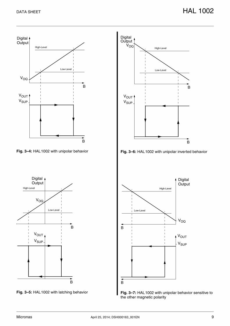
The HAL1002 is the improved successor of theHAL 1000 Hall switch. The major sensor characteris-tics, the two switching points BON and BOFF, are pro-grammable for the application. The sensor can be pro-grammed to be unipolar or latching, sensitive to themagnetic north pole or sensitive to the south pole, withnormal or with an electrically inverted output signal.Several examples are shown in Fig. 3–4 throughFig. 3–7.
The HAL1002 is based on the HAL83x family and fea-tures a temperature-compensated Hall plate withchoppered offset compensation, an A/D converter, dig-ital signal processing, a push-pull output stage, anEEPROM memory with redundancy and lock functionfor the calibration data, a serial interface for program-ming the EEPROM, and protection devices at all pins.Internal digital signal processing is of great benefitbecause analog offsets, temperature shifts, andmechanical stress effects do not degrade the sensoraccuracy.
The HAL1002 is programmable by modulating thesupply voltage. No additional programming pin isneeded. Programming is simplified through the use ofa 2-point calibration. Calibration is accomplished byadjusting the sensor output directly to the input signal.Individual adjustment of each sensor during the cus-tomer’s manufacturing process is possible. With thiscalibration procedure, the tolerances of the sensor, themagnet, and the mechanical positioning can be com-pensated for the final assembly. This offers a low-costalternative for all applications that presently requiremechanical adjustment or other system calibration.
In addition, the temperature compensation of the HallIC can be tailored to all common magnetic materials byprogramming first and second order temperature coef-ficients of the Hall sensor sensitivity. This enablesoperation over the full temperature range with constantswitching points.
The calculation of the individual sensor characteristicsand the programming of the EEPROM memory can easilybe done with a PC and the application kit from Micronas.
The sensor is designed and produced in sub-micronCMOS technology for the use in hostile industrial andautomotive applications with nominal supply voltage of5 V in the ambient temperature range from 40 °C upto 150 °C.
The HAL1002 is available in the leaded packageTO92UT-2.
1.1. Major Applications
Due to the sensor’s versatile programming characteris-tics, the HAL1002 is the optimal system solution forapplications which require very precise contactlessswitching:
– Endpoint detection
– Level switch (e.g. liquid level)
– Electronic fuse (current measurement)
1.2. Features
– High-precision Hall switch with programmable switching points and switching behavior
– AEC-Q100 qualified
– EMC and ESD optimized designESD HBM performance >7 kV
– Switching points programmable from 150 mT up to 150 mT in steps of 0.5% of the magnetic field range
– Multiple programmable magnetic characteristics in a non-volatile memory (EEPROM) with redundancy and lock function
– Temperature characteristics are programmable for matching all common magnetic materials
– Programming through a modulation of the supply voltage
– Operates from 40 °C up to 150 °C ambient temperature
– Operates from 4.5 V up to 8.5 V supply voltage in specification and functions up to 11 V
– Operates with static magnetic fields and dynamic magnetic fields up to 2 kHz
– Magnetic characteristics are extremely robust against mechanical stress effects
– Overvoltage and reverse-voltage protection at all pins
– Short-circuit protected push-pull output
4 April 25, 2014; DSH000163_001EN Micronas

DATA SHEET HAL 1002
2. Ordering Information
2.1. Marking Code
The HAL1002 has a marking on the package surface(branded side). This marking includes the name of thesensor and the temperature range.
2.2. Operating Junction Temperature Range (TJ)
The Hall sensors from Micronas are specified to thechip temperature (junction temperature TJ).
A: TJ = 40 °C to +170 °C
The relationship between ambient temperature (TA)and junction temperature is explained in Section 5.3.on page 21.
2.3. Hall Sensor Package Codes
Example: HAL1002UT-A
Type: 1002 Package: TO92UT Temperature Range: TJ = 40 °C to +170 °C
Hall sensors are available in a wide variety of packag-ing versions and quantities. For more detailed informa-tion, please refer to the brochure: “Hall Sensors:Ordering Codes, Packaging, Handling”.
Type Temperature Range
A
HAL1002 1002A
HALXXXXPA-T
Temperature Range: A Package: UT for TO92UT-1/-2Type: 1002
Micronas April 25, 2014; DSH000163_001EN 5

HAL 1002 DATA SHEET
3. Functional Description
3.1. General Function
The HAL1002 is a monolithic integrated circuit whichprovides a digital output signal. The sensor is basedon the HAL83x design.
The Hall plate is sensitive to magnetic north and southpolarity. The external magnetic field componentperpendicular to the branded side of the packagegenerates a Hall voltage. This voltage is converted to adigital value and processed in the Digital SignalProcessing Unit (DSP) according to the settings of theEEPROM registers. The function and the parametersfor the DSP are explained in Section 3.2. on page 8.
The setting of the LOCK register disables theprogramming of the EEPROM memory for all time.This register cannot be reset.
As long as the LOCK register is not set, the outputcharacteristic can be adjusted by programming theEEPROM registers. The IC is addressed bymodulating the supply voltage (see Fig. 3–1). Afterdetecting a command, the sensor reads or writes thememory and answers with a digital signal on the outputpin. The digital output is switched off during thecommunication.
Internal temperature compensation circuitry and thechoppered offset compensation enable the operationover the full temperature range with minimal changesof the switching points. The circuitry also rejects offsetshifts due to mechanical stress from the package. Thenon-volatile memory consists of redundant EEPROMcells. In addition, the HAL1002 is equipped withdevices for overvoltage and reverse-voltage protectionat all pins.
Fig. 3–1: Programming with VSUP modulation
VO
UT (
V)
5
6
7
8
VS
UP (
V)
HAL1002
VSUPGND
OUT
VSUP
6 April 25, 2014; DSH000163_001EN Micronas

DATA SHEET HAL 1002
Fig. 3–2: HAL1002 block diagram
Fig. 3–3: Details of EEPROM Registers and Digital Signal Processing
InternallyTemperature
Oscillator
Switched100 Digital OUT
VSUP
GND
SupplyEEPROM Memory
Lock Control
Digital
stabilizedSupply andProtectionDevices
DependentBias
ProtectionDevices
Hall PlateSignalProcessing
LevelDetection
OutputA/DConverter
Mode RegisterFilter
TC
5 bit
TCSQ
3 bit
Sensitivity
14 bit
VOQ
11 bit
Lock
1 bit
Micronas
Register2 bitRange3 bit
EEPROM Memory
A/DConverter
DigitalFilter
Multiplier AdderLimiter
Digital Signal Processing
ADC-Readout Register12 bit
Lock
Control
12 bit
Digital Output
Other: 5 bitTC Range Select 2 bit
Low HighLevel Level8 bit 9 bit
Comparator
Micronas April 25, 2014; DSH000163_001EN 7

HAL 1002 DATA SHEET
3.2. Digital Signal Processing and EEPROM
The DSP is the main part of the sensor and performsthe signal processing. The parameters for the DSP arestored in the EEPROM registers. The details areshown in Fig. 3–3.
Terminology:
SENSITIVITY: name of the register or register value
Sensitivity: name of the parameter
EEPROM Registers:
The EEPROM registers include three groups:
Group 1 contains the registers for the adaption of thesensor to the magnetic system: MODE for selectingthe magnetic field range and filter frequency, TC andTCSQ for the temperature characteristics of themagnetic sensitivity and thereby for the switchingpoints.
Group 2 contains the registers for defining theswitching points: SENSITIVITY, VOQ, LOW-LEVEL,and HIGH-LEVEL.
The comparator compares the processed signalvoltage with the reference values Low-Level and High-Level.
The output switches on (low) if the signal voltage ishigher than the High-Level, and switches off (high) ifthe signal falls below the Low-Level. Several examplesof different switching characteristics are shown inFig. 3–4 to Fig. 3–7.
– The parameter VOQ (Output Quiescent Voltage) cor-responds to the signal voltage at B = 0 mT.
– The parameter Sensitivity defines the magnetic sen-sitivity:
– The signal voltage can be calculated as follows:
Therefore, the switching points are programmed bysetting the SENSITIVITY, VOQ, LOW-LEVEL, andHIGH-LEVEL registers. The available Micronassoftware calculates the best parameter set respectingthe ranges of each register.
Group 3 contains the Micronas registers and LOCK forthe locking of all registers. The Micronas registers areprogrammed and locked during production and areread-only for the customer. These registers are usedfor oscillator frequency trimming, A/D converter offsetcompensation, and several other special settings.
VSignal
BSensitivity =
VSignal Sensitivity B + VOQ
8 April 25, 2014; DSH000163_001EN Micronas
DATA SHEET HAL 1002
Fig. 3–4: HAL1002 with unipolar behavior
Fig. 3–5: HAL1002 with latching behavior
Fig. 3–6: HAL1002 with unipolar inverted behavior
Fig. 3–7: HAL1002 with unipolar behavior sensitive to the other magnetic polarity
Digital
B
VOUT
B
VSUP
High-Level
Low-Level
VOQ
Output
B
VOUT
B
VSUP
High-Level
Low-Level
VOQ
DigitalOutput
Digital
B
VOUT
B
VSUP
High-Level
Low-Level
VOQ
Output
Digital
B
VOUT
B
VSUP
High-Level
Low-Level
VOQ
Output
Micronas April 25, 2014; DSH000163_001EN 9

HAL 1002 DATA SHEET
3.3. MODE register
The MODE register contains all bits used to configurethe A/D converter and the different output modes.
Offset Correction
The Offset Correction function can be used forhandling unipolar magnetic fields or systems with highmagnetic offset and small magnetic amplitudes. TheOFFSET CORRECTION register allows to adjust thedigital offset after the built-in A/D-converter. The digitaloffset can be programmed to 50%, 0% and 50% ofA/D-converter full-scale range.
For Offset correction please contact Micronas service.
Magnetic Range
The RANGE bits define the magnetic field range of the A/D converter.
Filter
The FILTER bits define the 3 dB frequency of thedigital low pass filter.
MODE
Bit Number 9 8 7 6 5 4 3 2 1 0
Parameter RANGE Signed Offset Correction
OUTPUTMODE FILTER RANGE(together with bit 9)
Offset Correction
Table 3–1: MODE register of the HAL 1002
Offset Correction
OFFSET CORRECTION
MODE [8] MODE [0]
50% 0 1
0 0 0
50% 1 1
Magnetic Range RANGE
MODE [9] MODE [2:1]
15 mT 1 00
30 mT 0 00
Table 3–2: Magnetic Range
40 mT 1 10
60 mT 0 01
80 mT 0 10
100 mT 0 11
150 mT 1 11
3 dB Frequency MODE [4:3]
80 Hz 00
500 Hz 10
1 kHz 11
2 kHz 01
Magnetic Range RANGE
MODE [9] MODE [2:1]
Table 3–2: Magnetic Range
10 April 25, 2014; DSH000163_001EN Micronas

DATA SHEET HAL 1002
Output Format
The OUTPUTMODE bits define the different outputmodes of HAL1002.
TC Register
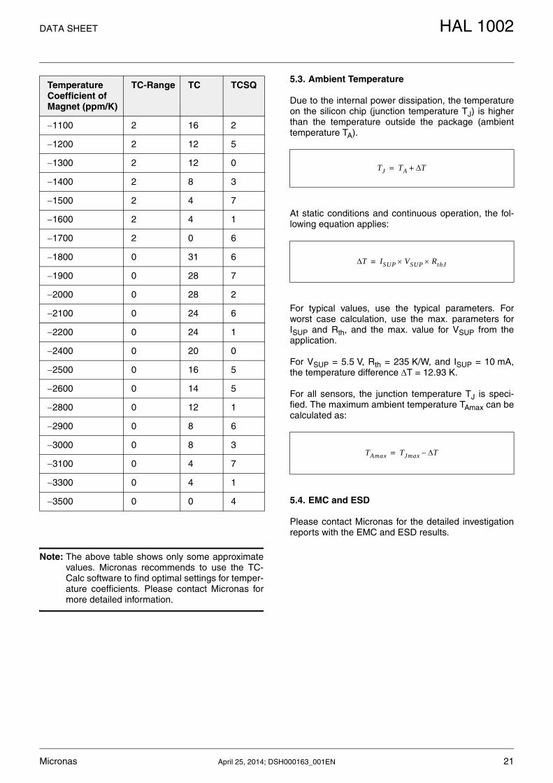
The temperature dependence of the magneticsensitivity can be adapted to different magneticmaterials in order to compensate for the change of themagnetic strength with temperature. The adaptation isdone by programming the TC (TemperatureCoefficient) and the TCSQ registers (QuadraticTemperature Coefficient). Thereby, the slope and thecurvature of the temperature dependence of themagnetic sensitivity can be matched to the magnetand the sensor assembly. As a result, the outputvoltage characteristic can be constant over the fulltemperature range. The sensor can compensate forlinear temperature coefficients ranging from about 3100 ppm/K up to 1000 ppm/K and quadraticcoefficients from about -7 ppm/K² to 2 ppm/K². The full TC range is separated in the following fourgroups:
TC (5 bit) and TCSQ (3 bit) have to be selectedindividually within each of the four ranges. For example0 ppm/k requires TC-Range = 1, TC = 15 and TCSQ =1. Please refer to Section 5.2. on page 20 for moredetails.
Sensitivity Register
The SENSITIVITY register contains the parameter forthe multiplier in the DSP. Sensitivity is programmablebetween 4 and 4 in steps of 0.00049. Sensitivity = 1corresponds to an increase of the signal voltage byVSUP if the ADC-READOUT increases by 2048.
VOQ Register
The VOQ register contains the parameter for the adderin the DSP. VOQ is the signal voltage without externalmagnetic field (B = 0 mT, respectivelyADC-READOUT = 0) and programmable from VSUPup to VSUP. For VSUP = 5 V, the register can bechanged in steps of 4.9 mV.
Note: If VOQ is programmed to a negative voltage, themaximum signal voltage is limited to:
Reference Level Register
The LOW-LEVEL and HIGH-LEVEL registers containthe reference values of the comparator.
The Low-Level is programmable between 0 V andVSUP/2. The register can be changed in steps of2.44 mV. The High-Level is programmable between0 V and VSUP in steps of 2.44 mV.
The four parameters Sensitivity, VOQ, Low-Level, andHigh-Level define the switching points BON and BOFF.For calibration in the system environment, a 2-pointadjustment procedure is recommended (seeSection 3.4.). The suitable parameter set for eachsensor can be calculated individually by this procedure.
GP Register
This register can be used to store information, likeproduction date or customer serial number. Micronaswill store production lot number, wafer number and x,ycoordinates in registers GP1 to GP3. The total registercontains four blocks with a length of 13 bit each.Thecustomer can read out this information and store it inhis production data base for reference or he can storeown production information instead.
Note: This register is not a guarantee for traceabilitybecause readout of registers is not possibleafter locking the IC.
To read/write this register it is mandatory toread/write all GP register one after the otherstarting with GP0. In case of a writing the regis-ters it necessary to first write all registers fol-lowed by one store sequence at the end. Even ifonly GP0 should be changed all other GP regis-ters must first be read and the read out datamust be written again to these registers.
Output Format MODE [7:5]
Switch (positive polarity) 100
Switch (negative polarity) 101
Table 3–3: OUTPUTMODE
TC-Range [ppm/k] GROUP
3100 to 1800 0
1750 to 550 2
500 to +450 (default value) 1
+450 to +1000 3
VSignal max = VOQ + VSUP
Micronas April 25, 2014; DSH000163_001EN 11

HAL 1002 DATA SHEET
LOCK Register
By setting the LSB of this 2-bit register, all registers willbe locked, and the sensor will no longer respond toany supply voltage modulation. This bit is active afterthe first power-off and power-on sequence after settingthe LOCK bit. After locking of sensor is active, it will nolonger respond to power supply modulation.
Warning: This register cannot be reset!
ADC-READOUT Register
This 14-bit register delivers the actual digital value ofthe applied magnetic field after filtering but before thesignal processing. This register can be read out and isthe basis for the calibration procedure of the sensor inthe system environment.
D/A-READOUT
This 14-bit register delivers the actual digital value ofthe applied magnetic field after the signal processing.
This register can be read out and is the basis for thecalibration procedure of the sensor in the systemenvironment.
Note: The MSB and LSB are reversed compared withall the other registers. Please reverse this regis-ter after readout.
Note: During calibration it is mandatory to select theAnalog Output as output format.The D/A-Read-out register can be read out only in the outputmode. For all other modes the result read backfrom the sensor will be a 0. After the calibrationthe output format can than easily be switched tothe wanted output mode.
3.4. General Calibration Procedure
For calibration in the system environment, theapplication kit from Micronas is recommended. Itcontains the hardware for the generation of the serialtelegram for programming and the correspondingsoftware for the input or calculation of the registervalues.
In this section, the programming of the sensor usingthis tool is explained. Please refer to Section 5. onpage 24 for information about programming withoutthis tool.
For the individual calibration of each sensor in thecustomer‘s application, a two-point adjustment isrecommended (see Fig. 3–1 for an example). Whenusing the application kit, the calibration can be done inthree steps:
Step 1: Input of the registers which need not be adjusted individually
The magnetic circuit, the magnetic material with itstemperature characteristics, and the filter frequency,are given for this application.
Therefore, the values of the following registers shouldbe identical for all sensors in the application.
– FILTER (according to maximum signal frequency)The 500 Hz range is recommended for highest accuracy.
– RANGE(according to the maximum magnetic field at the sensor position)
– TC and TCSQ(depends on the material of the magnet and the other temperature dependencies of the application)
Write the appropriate settings into the HAL1002registers.
Step 2: Calculation of the Sensor Parameters
Fig. 3–1 shows the typical characteristics for acontactless switch. There is a mechanical range wherethe sensor must be switched high and where thesensor must be switched low.
Set the system to the calibration point where thesensor output must be high, and press the key“Readout BOFF”. The result is the correspondingADC-READOUT value.
Note: The magnetic south pole on the branded sidegenerates negative ADC-READOUT values, thenorth polarity positive values.
Then, set the system to the calibration point where thesensor output must be low, press the key “ReadoutBON” and get the second ADC-READOUT value.
Now, adjust the hysteresis to the desired value. Thehysteresis is the difference between the switchingpoints and suppresses oscillation of the output signal.With 100% hysteresis, the sensor will switch low andhigh exactly at the calibration points. A lower value willadjust the switching points closer together. Fig. 3–1shows an example with 80% hysteresis.
12 April 25, 2014; DSH000163_001EN Micronas

DATA SHEET HAL 1002
By pressing the key “calibrate and store”, the softwarewill calculate the corresponding parameters forSensitivity, VOQ, Low-Level, High-Level and storesthese values in the EEPROM.
This calibration must be done individually for eachsensor.
The sensor is now calibrated for the customerapplication. However, the programming can bechanged again and again if necessary.
Fig. 3–1: Characteristics of a position switch
Step 3: Locking the Sensor
The last step is activating the LOCK function with the“lock” key. The sensor is now locked and does notrespond to any programming or reading commands.
Warning: The LOCK register cannot be reset!
3.5. Example: Calibration of a Position Switch
The following description explains the calibrationprocedure using a position switch as an example:
– The mechanical switching points are given.
– temperature coefficient of the magnet: 500 ppm/K
Step 1: Input of the registers which need not be adjusted individually
The register values for the following registers are givenfor all sensors in the application:
– FILTER Select the filter frequency: 500 Hz
– RANGESelect the magnetic field range: 30 mT
– TC For this magnetic material: 6
– TCSQFor this magnetic material: 14
Enter these values in the software and use the “writeand store” command to store these valuespermanently in the registers.
Step 2: Calculation of the Sensor Parameters
Set the system to the calibration point where thesensor output must be high and press “Readout BOFF”.
Set the system to the calibration point where thesensor output must be low and press “Readout BON”.
Now, adjust the hysteresis to 80% and press the key“calibrate and store”.
Step 3: Locking the Sensor
The last step is activating the LOCK function with the“LOCK” command. The sensor is now locked and doesnot respond to any programming or readingcommands. Please note that the LOCK functionbecomes effective after power-down and power-up ofthe Hall-IC.
Warning: The LOCK register cannot be reset!
Sensor switched on
VOUT
position
Sensor switched off
Calibration points
Sensor switched on
Hysteresis
(here 80 %)
Micronas April 25, 2014; DSH000163_001EN 13

HAL 1002 DATA SHEET
4. Specifications
4.1. Outline Dimensions
Fig. 4–1:TO92UT-2 Plastic Transistor Standard UT package, 3 leadsWeight approximately 0.12 g
Θ
DRAWING-NO.
06615.0001.4
solderability is guaranteed between end of pin and distance F1.
A4, Bd, y= these dimensions are different for each sensor type and are specified in the data sheet.
0.36mm1.551.45
0.7 0.42
JEDEC STANDARD
ISSUE
-
ITEM NO.
-
A3UNIT A2 b c
4.054.114.01
1.20.8
0.600.42
1.2714.5min
ANSI
10-04-29
ISSUE DATEYY-MM-DD
D1 e E1 F2F1 L
45°
ZG-NO.
ZG001015_Ver.07
2.50
Θ
scale
5 mm
D1
L
e b
F2
1 2 3
F1
c
Bd
Center of sensitive area
E1
y
A4
A2
A3
physical dimensions do not include moldflash.
min/max of D1 are specified in the datasheet.
Sn-thickness might be reduced by mechanical handling.
14 April 25, 2014; DSH000163_001EN Micronas

DATA SHEET HAL 1002
Fig. 4–2:TO92UA/UT: Dimensions ammopack inline, not spread
Micronas April 25, 2014; DSH000163_001EN 15

HAL 1002 DATA SHEET
4.2. Soldering, Welding and Assembly
Please check the Micronas Document “Guidelines for the Assembly of HAL Packages” for further information aboutsolderability, welding, assembly, and second-level packaging. The document is available on the Micronas website oron the service portal.
4.3. Pin Connections and Short Descriptions
Fig. 4–3: Pin configuration
4.4. Dimension of Sensitive Area
0.25 mm x 0.25 mm
4.5. Physical Dimensions
Pin No.
Pin Name Short Description
1 VSUP Supply Voltage andProgramming Pin
2 GND Ground
3 OUT Push-Pull Output and Selection Pin
1
2
3
VSUP
OUT
GND
TO92UT-1/-2
A4 0.3 mm nominal
Bd 0.3 mm
D1 4.05 mm ± 0.05 mm
H1 min. 22.0 mmmax. 24.1 mm
y 1.5 mm nominal
16 April 25, 2014; DSH000163_001EN Micronas

DATA SHEET HAL 1002
4.6. Absolute Maximum Ratings
Stresses beyond those listed in the “Absolute Maximum Ratings” may cause permanent damage to the device. Thisis a stress rating only. Functional operation of the device at these conditions is not implied. Exposure to absolutemaximum rating conditions for extended periods will affect device reliability.
This device contains circuitry to protect the inputs and outputs against damage due to high static voltages or electricfields; however, it is advised that normal precautions be taken to avoid application of any voltage higher than abso-lute maximum-rated voltages to this circuit.
All voltages listed are referenced to ground (GND).
Symbol Parameter Pin No. Min. Max. Unit Condition
VSUP Supply Voltage 1 8.5 11 V t < 96 h3)
VSUP Supply Voltage 1 16 16 V t < 1 h3)
VOUT Output Voltage 3 5 16 V
VOUT VSUP Excess of Output Voltage over Supply Voltage
3,1 2 V
IOUT Continuous Output Current 3 10 10 mA
tSh Output Short Circuit Duration 3 10 min
VESD ESD Protection1) 13
8.07.5
8.07.5
kV
TJ Junction Temperature under bias2)
50 190 °C
1) AEC-Q100-002 (100 pF and 1.5 k)2) For 96 h - Please contact Micronas for other temperature requirements3) No cumulated stress
Micronas April 25, 2014; DSH000163_001EN 17

HAL 1002 DATA SHEET
4.6.1. Storage and Shelf Life
The permissible storage time (shelf life) of the sensors is unlimited, provided the sensors are stored at a maximum of30 °C and a maximum of 85% relative humidity. At these conditions, no Dry Pack is required.
Solderability is guaranteed for two years from the date code on the package.
4.7. Recommended Operating Conditions
Functional operation of the device beyond those indicated in the “Recommended Operating Conditions/Characteris-tics” is not implied and may result in unpredictable behavior, reduce reliability and lifetime of the device.
All voltages listed are referenced to ground (GND).
Symbol Parameter Pin No. Min. Typ. Max. Unit Condition
VSUP Supply Voltage 1 4.5 5 8.5 V
IOUT Continuous Output Current 3 1.2 1.2 mA
RL Load Resistor 3 5.0 10 k Can be pull-up or pull-down resistor (analog output only)
CL Load Capacitance 3 0.33 100 1000 nF
NPRG Number of EEPROM Pro-gramming Cycles
100 cycles 0°C < Tamb < 55°C
TJ Junction Temperature Range1)
404040
125150170
°C°C°C
for 8000 h2)
for 2000 h2)
for 1000 h2)
1) Depends on the temperature profile of the application. Please contact Micronas for life time calculations.2) Time values are not cumulative
18 April 25, 2014; DSH000163_001EN Micronas

DATA SHEET HAL 1002
4.8. Characteristics
at TJ = 40 °C to +170 °C, VSUP = 4.5 V to 8.5 V, after programming and locking of the device,at Recommended Operation Conditions if not otherwise specified in the column “Conditions”.Typical Characteristics for TJ = 25 °C and VSUP = 5 V.
4.9. Magnetic Characteristics
at TJ = 40 °C to +170 °C, VSUP = 4.5 V to 8.5 V, GND = 0 V after programming and locking, at RecommendedOperation Conditions if not otherwise specified in the column “Conditions”.Typical Characteristics for TJ = 25 °C and VSUP = 5 V.
Symbol Parameter Pin No. Min. Typ. Max. Unit Conditions
IDD Supply Current over Temperature Range
1 7 10 mA
VOUTH Output High Voltage 3 4.65 4.8 V VSUP = 5 V, 1 mA IOUT 1 mA
VOUTL Output Low Voltage 3 0.2 0.35 V VSUP = 5 V, 1 mA IOUT 1 mA
fADC Internal ADC Frequency 120 128 140 kHz TJ = 25 °C
fADC Internal ADC Frequency over Temperature Range
110 128 150 kHz VSUP = 5 V
tr(O) Response Time of Output 3 5421
10842
msmsmsms
3 dB Filter frequency = 80 Hz3 dB Filter frequency = 160 Hz3 dB Filter frequency = 500 Hz3 dB Filter frequency = 2 kHzCL = 10 nF, time from 10% to 90% of final output voltage for a steplike signal Bstep from 0 mT to Bmax
td(O) Delay Time of Output 3 0.1 0.5 ms CL = 10 nF
tPOD Power-Up Time (Time to reach stabilized Output Voltage)
6532
11953
msmsmsms
3 dB Filter frequency = 80 Hz3 dB Filter frequency = 160 Hz3 dB Filter frequency = 500 Hz3 dB Filter frequency = 2 kHzCL = 10 nF, 90% of VOUT
BW Small Signal Bandwidth (3 dB)
3 2 kHz BAC < 10 mT;3 dB Filter frequency = 2 kHz
RthjaRthjcRthjs
Thermal Resistance
Junction to AmbientJunction to CaseJunction to Solder Point
23561159
K/W measured on a 1s0p boardmeasured on a 1s0p boardmeasured on a 1s1p board
BON_OFF_res Programming Resolution 12 bit including sign bit
BON_OFF_acc Threshold Accuracy 0.1 +0.1 % at TJ = 25 °C based on characterization
BON_OFF_acc Threshold Accuracy 4 +4 % over operating temperature rangebased on characterization
Symbol Parameter Pin No. Min. Typ. Max. Unit Test Conditions
BOffset Magnetic Offset 3 0.5 0 0.5 mT B = 0 mT, IOUT = 0 mA, TJ = 25 °C,unadjusted sensor
BOffset Magnetic Offset Drift 200 0 200 T B = 0 mT, IOUT = 0 mA
VSUP = 5 V; 60 mT range, 3db frequency = 500 Hz, TC = 15,TCSQ = 1, TC-Range = 10.65 < sensitivity < 0.65
Micronas April 25, 2014; DSH000163_001EN 19

HAL 1002 DATA SHEET
5. Application Notes
5.1. Application Circuit
For EMC protection, it is recommended to connect oneceramic 100 nF capacitor between ground and thesupply voltage, and between ground and the outputpin.
Please note that during programming, the sensor willbe supplied repeatedly with the programming voltageof 12.5 V for 100 ms. All components connected to theVSUP line at this time must be able to resist this volt-age.
Fig. 5–1: Recommended application circuit
For application circuits for high supply voltages, suchas 24 V, please contact the Micronas application ser-vice.
Fig. 5–2: Example for an application circuit for high supply voltage
5.2. Temperature Compensation
The relationship between the temperature coefficientof the magnet and the corresponding TC and TCSQcodes for linear compensation is given in the followingtable. In addition to the linear change of the magneticfield with temperature, the curvature can be adjustedas well. For this purpose, other TC and TCSQ combi-nations are required which are not shown in the table.Please contact Micronas for more detailed informationon this higher order temperature compensation.
The HAL83x and HAL1002 contain the same tempera-ture compensation circuits. If an optimal setting for theHAL83x is already available, the same settings may beused for the HAL1002.
OUT
VSUP
GND
100 nFHAL1002
OUT
VSUP
GND
Z1 HAL1002100 nF
R1
Temperature Coefficient of Magnet (ppm/K)
TC-Range TC TCSQ
1075 3 31 7
1000 3 28 1
900 3 24 0
750 3 16 2
675 3 12 2
575 3 8 2
450 3 4 2
400 1 31 0
250 1 24 1
150 1 20 1
50 1 16 2
0 1 15 1
100 1 12 0
200 1 8 1
300 1 4 4
400 1 0 7
500 1 0 0
600 2 31 2
700 2 28 1
800 2 24 3
900 2 20 6
1000 2 16 7
20 April 25, 2014; DSH000163_001EN Micronas
DATA SHEET HAL 1002
Note: The above table shows only some approximatevalues. Micronas recommends to use the TC-Calc software to find optimal settings for temper-ature coefficients. Please contact Micronas formore detailed information.
5.3. Ambient Temperature
Due to the internal power dissipation, the temperatureon the silicon chip (junction temperature TJ) is higherthan the temperature outside the package (ambienttemperature TA).
At static conditions and continuous operation, the fol-lowing equation applies:
For typical values, use the typical parameters. Forworst case calculation, use the max. parameters forISUP and Rth, and the max. value for VSUP from theapplication.
For VSUP = 5.5 V, Rth = 235 K/W, and ISUP = 10 mA,the temperature difference T = 12.93 K.
For all sensors, the junction temperature TJ is speci-fied. The maximum ambient temperature TAmax can becalculated as:
5.4. EMC and ESD
Please contact Micronas for the detailed investigationreports with the EMC and ESD results.
1100 2 16 2
1200 2 12 5
1300 2 12 0
1400 2 8 3
1500 2 4 7
1600 2 4 1
1700 2 0 6
1800 0 31 6
1900 0 28 7
2000 0 28 2
2100 0 24 6
2200 0 24 1
2400 0 20 0
2500 0 16 5
2600 0 14 5
2800 0 12 1
2900 0 8 6
3000 0 8 3
3100 0 4 7
3300 0 4 1
3500 0 0 4
Temperature Coefficient of Magnet (ppm/K)
TC-Range TC TCSQ
TJ TA T+=
T ISUP VSUP RthJ=
TAmax TJmax T–=
Micronas April 25, 2014; DSH000163_001EN 21
HAL 1002 DATA SHEET
6. Programming
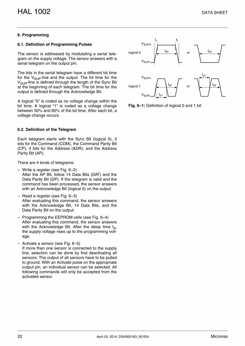
6.1. Definition of Programming Pulses
The sensor is addressed by modulating a serial tele-gram on the supply voltage. The sensor answers with aserial telegram on the output pin.
The bits in the serial telegram have a different bit timefor the VSUP-line and the output. The bit time for theVSUP-line is defined through the length of the Sync Bitat the beginning of each telegram. The bit time for theoutput is defined through the Acknowledge Bit.
A logical “0” is coded as no voltage change within thebit time. A logical “1” is coded as a voltage changebetween 50% and 80% of the bit time. After each bit, avoltage change occurs.
6.2. Definition of the Telegram
Each telegram starts with the Sync Bit (logical 0), 3bits for the Command (COM), the Command Parity Bit(CP), 4 bits for the Address (ADR), and the AddressParity Bit (AP).
There are 4 kinds of telegrams:
– Write a register (see Fig. 6–2)After the AP Bit, follow 14 Data Bits (DAT) and theData Parity Bit (DP). If the telegram is valid and thecommand has been processed, the sensor answerswith an Acknowledge Bit (logical 0) on the output.
– Read a register (see Fig. 6–3)After evaluating this command, the sensor answerswith the Acknowledge Bit, 14 Data Bits, and theData Parity Bit on the output.
– Programming the EEPROM cells (see Fig. 6–4)After evaluating this command, the sensor answerswith the Acknowledge Bit. After the delay time tw,the supply voltage rises up to the programming volt-age.
– Activate a sensor (see Fig. 6–5)If more than one sensor is connected to the supplyline, selection can be done by first deactivating allsensors. The output of all sensors have to be pulledto ground. With an Activate pulse on the appropriateoutput pin, an individual sensor can be selected. Allfollowing commands will only be accepted from theactivated sensor.
Fig. 6–1: Definition of logical 0 and 1 bit
tr tf
tp0 tp0logical 0
VSUPH
VSUPL
or
tp0logical 1
VSUPH
VSUPL
ortp0
tp1
tp1
22 April 25, 2014; DSH000163_001EN Micronas
DATA SHEET HAL 1002
Fig. 6–2: Telegram for coding a Write command
Fig. 6–3: Telegram for coding a Read command
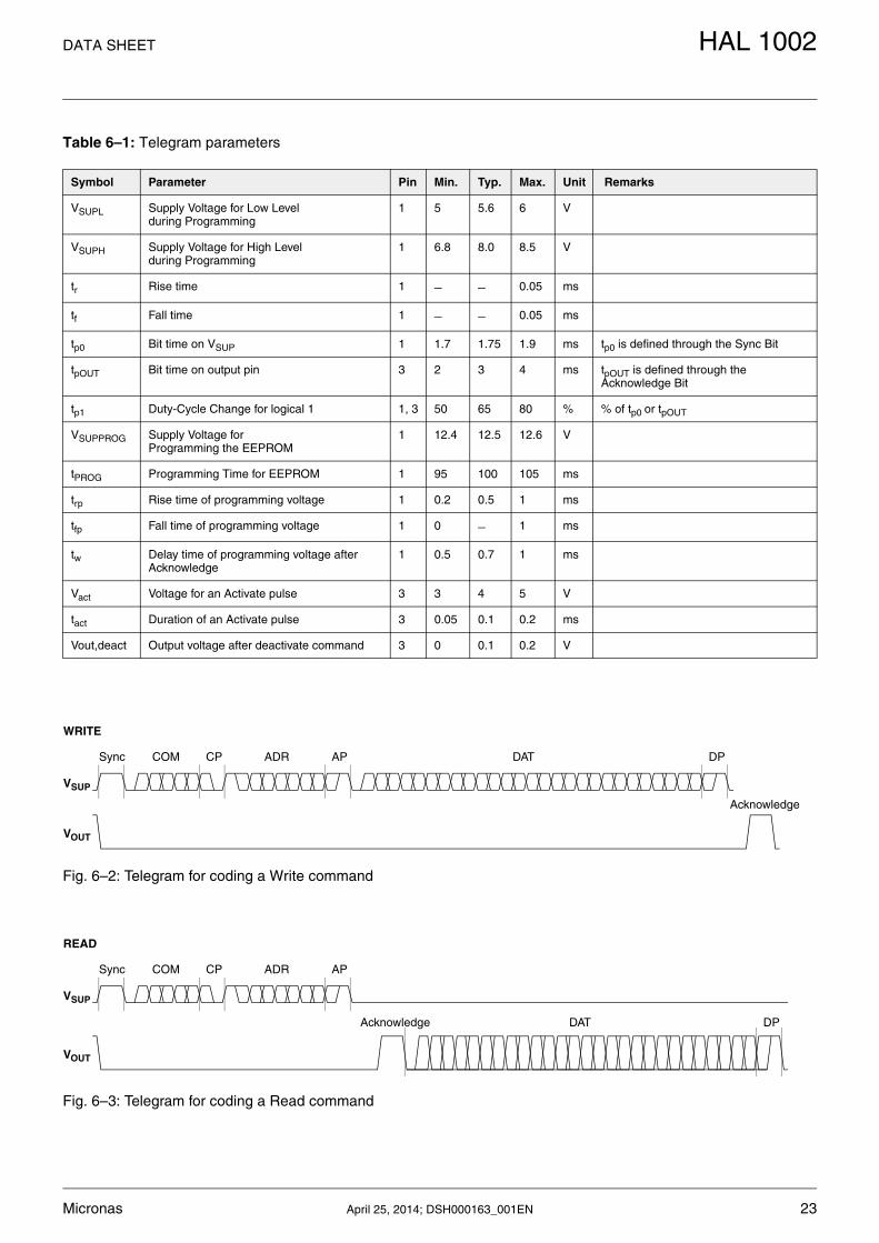
Table 6–1: Telegram parameters
Symbol Parameter Pin Min. Typ. Max. Unit Remarks
VSUPL Supply Voltage for Low Levelduring Programming
1 5 5.6 6 V
VSUPH Supply Voltage for High Levelduring Programming
1 6.8 8.0 8.5 V
tr Rise time 1 0.05 ms
tf Fall time 1 0.05 ms
tp0 Bit time on VSUP 1 1.7 1.75 1.9 ms tp0 is defined through the Sync Bit
tpOUT Bit time on output pin 3 2 3 4 ms tpOUT is defined through the Acknowledge Bit
tp1 Duty-Cycle Change for logical 1 1, 3 50 65 80 % % of tp0 or tpOUT
VSUPPROG Supply Voltage for Programming the EEPROM
1 12.4 12.5 12.6 V
tPROG Programming Time for EEPROM 1 95 100 105 ms
trp Rise time of programming voltage 1 0.2 0.5 1 ms
tfp Fall time of programming voltage 1 0 1 ms
tw Delay time of programming voltage after Acknowledge
1 0.5 0.7 1 ms
Vact Voltage for an Activate pulse 3 3 4 5 V
tact Duration of an Activate pulse 3 0.05 0.1 0.2 ms
Vout,deact Output voltage after deactivate command 3 0 0.1 0.2 V
Sync COM CP ADR AP DAT DP
Acknowledge
VSUP
VOUT
WRITE
Sync COM CP ADR AP
DAT DPAcknowledge
VSUP
VOUT
READ
Micronas April 25, 2014; DSH000163_001EN 23

HAL 1002 DATA SHEET
Fig. 6–4: Telegram for coding the EEPROM programming
Fig. 6–5: Activate pulse
6.3. Telegram Codes
Sync Bit
Each telegram starts with the Sync Bit. This logical “0”pulse defines the exact timing for tp0.
Command Bits (COM)
The Command code contains 3 bits and is a binarynumber. Table 6–2 shows the available commands andthe corresponding codes for the HAL 1002.
Command Parity Bit (CP)
This parity bit is “1” if the number of zeros within the 3Command Bits is uneven. The parity bit is “0”, if thenumber of zeros is even.
Address Bits (ADR)
The Address code contains 4 bits and is a binary num-ber. Table 6–3 shows the available addresses for theHAL 1002 registers.
Address Parity Bit (AP)
This parity bit is “1” if the number of zeros within the 4Address bits is uneven. The parity bit is “0” if the num-ber of zeros is even.
Data Bits (DAT)
The 14 Data Bits contain the register information.
The registers use different number formats for the DataBits. These formats are explained in Section 6.4.
In the Write command, the last bits are valid. If, forexample, the TC register (10 bits) is written, only thelast 10 bits are valid.
In the Read command, the first bits are valid. If, forexample, the TC register (10 bits) is read, only the first10 bits are valid.
Data Parity Bit (DP)
This parity bit is “1” if the number of zeros within thebinary number is even. The parity bit is “0” if the num-ber of zeros is uneven.
Acknowledge
After each telegram, the output answers with theAcknowledge signal. This logical “0” pulse defines theexact timing for tpOUT.
Sync COM CP ADR AP
tPROG
Acknowledge
VSUP
VOUT
ERASE, PROM, and LOCK
trp tfp
tw
VSUPPROG
tACT
VOUT
tr tfVACT
24 April 25, 2014; DSH000163_001EN Micronas

DATA SHEET HAL 1002
6.4. Number Formats
Binary number:
The most significant bit is given as first, the least signif-icant bit as last digit.
Example: 101001 represents 41 decimal.
Signed binary number:
The first digit represents the sign of the followingbinary number (1 for negative, 0 for positive sign).
Example: 0101001 represents +41 decimal1101001 represents 41 decimal
Two’s-complement number:
The first digit of positive numbers is “0”, the rest of thenumber is a binary number. Negative numbers startwith “1”. In order to calculate the absolute value of thenumber, calculate the complement of the remainingdigits and add “1”.
Example: 0101001 represents +41 decimal1010111 represents 41 decimal
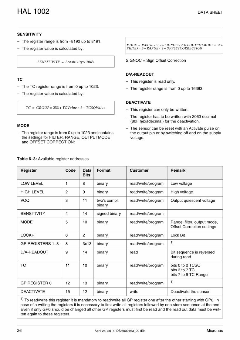
6.5. Register Information
LOW Level
– The register range is from 0 up to 255.
– The register value is calculated by:
HIGH Level
– The register range is from 0 up to 511.
– The register value is calculated by:
VOQ
– The register range is from 1024 up to 1023.
– The register value is calculated by:
Table 6–2: Available commands
Command Code Explanation
READ 2 read a register
WRITE 3 write a register
PROM 4 program all nonvolatile registers (except the lock bits)
ERASE 5 erase all nonvolatile registers (except the lock bits)
LOW LevelLow-Level Voltage 2
VSUP-------------------------------------------------------- 255=
HIGH LevelHigh-Level Voltage
VSUP------------------------------------------------ 511=
VOQVOQ
VSUP------------- 1024=
Micronas April 25, 2014; DSH000163_001EN 25
HAL 1002 DATA SHEET
SENSITIVITY
– The register range is from 8192 up to 8191.
– The register value is calculated by:
TC
– The TC register range is from 0 up to 1023.
– The register value is calculated by:
MODE
– The register range is from 0 up to 1023 and contains the settings for FILTER, RANGE, OUTPUTMODE and OFFSET CORRECTION:
SIGNOC = Sign Offset Correction
D/A-READOUT
– This register is read only.
– The register range is from 0 up to 16383.
DEACTIVATE
– This register can only be written.
– The register has to be written with 2063 decimal (80F hexadecimal) for the deactivation.
– The sensor can be reset with an Activate pulse on the output pin or by switching off and on the supply voltage.
SENSITIVITY Sensitivity 2048=
TC GROUP 256 TCValue 8 TCSQValue++=
MODE RANGE 512 SIGNOC 256+ OUTPUTMODE+ 32FILTER 8 RANGE 2 OFFSETCORRECTION++
+=
Table 6–3: Available register addresses
Register Code Data Bits
Format Customer Remark
LOW LEVEL 1 8 binary read/write/program Low voltage
HIGH LEVEL 2 9 binary read/write/program High voltage
VOQ 3 11 two’s compl. binary
read/write/program Output quiescent voltage
SENSITIVITY 4 14 signed binary read/write/program
MODE 5 10 binary read/write/program Range, filter, output mode, Offset Correction settings
LOCKR 6 2 binary read/write/program Lock Bit
GP REGISTERS 1..3 8 3x13 binary read/write/program 1)
D/A-READOUT 9 14 binary read Bit sequence is reversed during read
TC 11 10 binary read/write/program bits 0 to 2 TCSQbits 3 to 7 TCbits 7 to 9 TC Range
GP REGISTER 0 12 13 binary read/write/program 1)
DEACTIVATE 15 12 binary write Deactivate the sensor
1) To read/write this register it is mandatory to read/write all GP register one after the other starting with GP0. In case of a writing the registers it is necessary to first write all registers followed by one store sequence at the end. Even if only GP0 should be changed all other GP registers must first be read and the read out data must be writ-ten again to these registers.
26 April 25, 2014; DSH000163_001EN Micronas
DATA SHEET HAL 1002
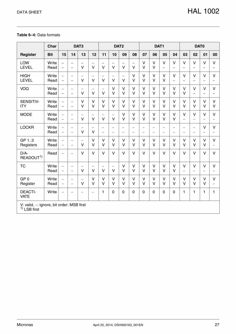
Table 6–4: Data formats
Register
Char DAT3 DAT2 DAT1 DAT0
Bit 15 14 13 12 11 10 09 08 07 06 05 04 03 02 01 00
LOWLEVEL
WriteRead
V
V
V
V
V
V
VV
VV
V
V
V
V
V
V
HIGHLEVEL
WriteRead
V
V
V
V
V
VV
VV
VV
VV
V
V
V
V
V
VOQ WriteRead
V
V
V
VV
VV
VV
VV
VV
VV
VV
VV
V
V
V
SENSITIV-ITY
WriteRead
VV
VV
VV
VV
VV
VV
VV
VV
VV
VV
VV
VV
VV
VV
MODE WriteRead
V
V
V
V
VV
VV
VV
VV
VV
VV
V
V
V
V
LOCKR WriteRead
V
V
V
V
GP 1..3Registers
WriteRead
V
VV
VV
VV
VV
VV
VV
VV
VV
VV
VV
VV
VV
V
D/A-READOUT1)
Read V V V V V V V V V V V V V V
TC WriteRead
V
V
V
V
VV
VV
VV
VV
VV
VV
V
V
V
V
GP 0Register
WriteRead
V
VV
VV
VV
VV
VV
VV
VV
VV
VV
VV
VV
VV
V
DEACTI-VATE
Write 1 0 0 0 0 0 0 0 1 1 1 1
V: valid, : ignore, bit order: MSB first1) LSB first
Micronas April 25, 2014; DSH000163_001EN 27

HAL 1002 DATA SHEET
6.6. Programming Information
If the content of any register (except the lock registers)is to be changed, the desired value must first be writ-ten into the corresponding RAM register. Before read-ing out the RAM register again, the register value mustbe permanently stored in the EEPROM.
Permanently storing a value in the EEPROM is doneby first sending an ERASE command followed bysending a PROM command. The address within theERASE and PROM commands must be zero.ERASE and PROM act on all registers in parallel.
If all HAL 1002 registers are to be changed, all writingcommands can be sent one after the other, followed bysending one ERASE and PROM command at the end.
During all communication sequences, the customerhas to check if the communication with the sensor wassuccessful. This means that the acknowledge and theparity bits sent by the sensor have to be checked bythe customer. If the Micronas programmer board isused, the customer has to check the error flags sentfrom the programmer board.
Note: For production and qualification tests it is man-datory to set the LOCK bit after final adjustmentand programming of HAL 1002. The LOCK func-tion is active after the next power-up of the sen-sor. The success of the lock process shall bechecked by reading at least one sensor registerafter locking and/or by an analog check of thesensors output signal.Electrostatic discharges (ESD) may disturb theprogramming pulses. Please take precautionsagainst ESD.
28 April 25, 2014; DSH000163_001EN Micronas

HAL 1002 DATA SHEET
29 April 25, 2014; DSH000163_001EN Micronas
Micronas GmbHHans-Bunte-Strasse 19 D-79108 Freiburg P.O. Box 840 D-79008 Freiburg, Germany
Tel. +49-761-517-0 Fax +49-761-517-2174 E-mail: [email protected] Internet: www.micronas.com
7. Data Sheet History
1. Preliminary Data Sheet “HAL 1002 Highly Precise Programmable Hall-Effect Switch”, Dec. 13, 2013, PD000214_001EN. First release of the preliminary data sheet.
2. Data Sheet “HAL 1002 Highly Precise Programma-ble Hall-Effect Switch”, April 25, 2014, DSH000163_001EN. First release of the data sheet.
Major Changes:
– Block diagram updated
– Parameter values for Programming Resolutionand Threshold Accuracy added