Guidelines for Selection, Screening and Qualification of ...
19
1 NASA Electronic Parts and Packaging (NEPP) Program NEPP Task: Screening Techniques for Ceramic Capacitors Guidelines for Selection, Screening and Qualification of Low-Voltage Commercial Multilayer Ceramic Capacitors for Space Programs Rev. A Alexander Teverovsky Dell Perot Systems Code 562, NASA GSFC, Greenbelt, MD 20771 [email protected] 2012
Transcript of Guidelines for Selection, Screening and Qualification of ...

1
NASA Electronic Parts and Packaging (NEPP) Program
NEPP Task:
Screening Techniques for Ceramic Capacitors
Guidelines for Selection, Screening and Qualification of Low-Voltage
Commercial Multilayer Ceramic Capacitors for Space Programs
Rev. A
Alexander Teverovsky
Dell Perot Systems
Code 562, NASA GSFC, Greenbelt, MD 20771 [email protected]
2012

2
Guidelines for selection, screening and qualification of low-voltage commercial ceramic capacitors for space programs Preface.
This document has been developed in the course of NASA Electronic Parts and Packaging (NEPP) program and is not an official endorsement of the insertion of commercial capacitors in space programs or an established set of requirements for their testing. The purpose of this document is to suggest possible ways for selection, screening, and qualification of commercial capacitors for NASA projects and open discussions in the parts engineering community related to the use of COTS ceramic capacitors.
I. Scope. This guideline is applicable to commercial surface mount chip, simple parallel plate design, multi-layer ceramic capacitors (MLCCs) rated to voltages of 100V and less. Parts with different design, e.g. low inductance ceramic capacitors (LICA), land grid array (LGA) etc., might need additional testing and tailoring of the requirements described in this document. Although the focus of this document is on commercial MLCCs, many procedures discussed below would be beneficial for military-grade capacitors.
II. Background. Hundreds of billions of commercial ceramic capacitors are operating successfully for many years in consumer electronics and industry including multiple automotive and medical applications in which the health and safety of people depend on quality and reliability of components. This is the most convincing evidence that commercial capacitors can operate reliably in space systems provided they are properly selected, screened, qualified, and derated.
Design of commercial MLCCs is driven by two factors: cost reduction and increase in performance, specifically, the volumetric efficiency of capacitors. The first, resulted in replacement of the precious metal electrodes, PME, made of silver/palladium alloys with the base metal electrodes, BME, made of nickel. The second, forced manufacturers to decrease the thickness of dielectric layers (down to micrometer range size), use new compositions of ceramics having greater dielectric constants, increase the number of electrode plates (up to several hundred), decrease side and end margins, and reduce the thickness of the cover plates. These design changes might have serious reliability implications.

3
Replacement of Ag/Pd electrodes with Ni requires high-temperature processing in reducing atmosphere to prevent nickel oxidation that results in increased concentration of oxygen vacancies in the ceramic. This might raise conductivity of ceramic materials by orders of magnitude and to prevent degradation of the insulation resistance (IR) special barium titanate-based compositions that are capable of withstanding annealing in reducing atmospheres have been developed.
Another problem associated with BME capacitors is migration of the charged oxygen vacancies with time under electrical bias that might result in a decrease of IR and parametric failures with time of operation or during life testing. This degradation limited applications of first BME capacitors built approximately 20 years ago and until recently was the major barrier for their employment in high-reliability systems. Substantial improvements in the materials and processing that have been made over last years allowed reducing the rate of degradation to an acceptable level.
Degradation of IR still can be observed at extremely high temperatures and voltages during highly accelerated life testing (HALT). Acceleration factors for reliability testing of ceramic capacitors are typically calculated using an empirical Prokopowicz-Vaskas equation:
−×
==
211
2
222
111 11exp),(),(
TTkE
VV
TVTVAF a
n
ττ (1)
where τ2 is the duration of testing at voltage V2 and temperature T2 that is equivalent to the duration of test during a period of τ1 at voltage V1 and temperature T1, n is the voltage acceleration constant, Ea is the activation energy, k is the Boltzmann’s constant.
Experience shows that voltage and temperature acceleration factors for IR degradation are larger for BME capacitors compared to traditional PME parts. For PME capacitors the acceleration constant n is approximately 3 and the activation energy is in the range from 0.9 eV to 1 eV. For BME capacitors Ea is in the range from 1 eV to ~ 1.8 eV and n is between 4 and 9. At these parameters of the model the acceleration factors are large, and a 96-hour testing of capacitors at 2 times rated voltage (VR) and 125 °C during voltage conditioning (a typical screening procedure) would be equivalent to testing at operating conditions (assumed 50 °C and 0.5 VR) to more than a thousand years of operation (see Figure 1).
Note that the rated voltage of low-voltage ceramic capacitors is determined by their polarization characteristics and is not related to electrical breakdown that is typically 10 to 100 times greater than VR. This allows performing HALT at extremely high voltages compared to the rated voltage and results in enormous acceleration of the degradation processes. In many cases application conditions for capacitors are rather benign and the operating voltages are far below the derating requirement of 0.5 VR. This decreases even further the possibility of failures related to the presence of oxygen vacancies and makes using a relatively short-term life testing sufficient

4
to assure that no wear-out failures would occur during the mission. Obviously, derating is a most powerful mitigation measure for reduction of risks related to the presence of oxygen vacancies in BME capacitors.
High brittleness of barium titanate ceramic materials that are used in capacitors in combination with thermal and mechanical stresses associated with assembly process and mechanical testing makes all chip ceramic capacitors susceptible to fracturing which is a major reason for field and qualification test failures for both, commercial and military-grade MLCCs. Increased volumetric efficiency of commercial capacitors is often achieved by reducing the size of non-active areas that makes them more vulnerable to crack-related failures. Soldering-induced thermal shock and board flexing (during handling of the boards or vibration testing) create fractures mostly at margin areas of capacitors that experience the highest level of stress. The marginal areas have also substantial levels of built-in stresses and increased concentration of processing-related defects thus facilitating crack formation. When the thickness of the cover plate and size of the edge margin are large, cracks have a lesser probability to extend into the active areas and cause IR degradation or failures.
Leakage currents in capacitors with cracks increase with time under bias and in some cases might result in short circuit failures after months or years of operation. In many cases the level of leakage current in fractured capacitors is below the sensitivity of the circuit; however, such capacitors are not stable and might generate excessive noise causing errors and malfunctions in the system that are difficult to troubleshoot.
Silver in the silver-palladium alloys used for electrodes in military-grade MLCCs is much more susceptible to electrochemical migration and dendrite growth compared to nickel that is used for most of commercial capacitors. For this reason commercial BME parts with cracks might be less susceptible to short circuit failures compared to PME capacitors.
Crack-related degradation processes can be accelerated with voltage and humidity of the environments. However, electrochemical processes in cracks that cause degradation of IR and failures occur even at relatively low humidity. Water sorption and capillary condensation in cracks can occur at room conditions and moisture that is adsorbed on the surface of cracks in ceramics can be released at extremely large temperatures only. Although applied voltage accelerates degradation processes in cracks, the conductive path created in the crack by moisture or as a result of electrochemical processes at the electrodes can be destroyed when a short is formed (blowing fuse effect). After that, leakage current might start increasing again, so leakage currents in the part behave erratically and create excessive noise in the system. Increase in temperature accelerates electrochemical processes and ion migration, but might impede degradation by reducing the amount of moisture absorbed in the crack, so there are no established acceleration factors for crack-related failure mechanisms. Note also that degradation processes in capacitors with cracks can occur at low voltages, so voltage and temperature derating is not as effective as in the case of IR degradation related to migration of oxygen

5
vacancies. For this reason the risk of failures should be mitigated by a proper selection and qualification testing of the parts and by a thorough control over the assembly process and post-assembly handling of the boards.
III. Part selection and construction analysis/DPA
Recommendations for selection of commercial MLCCs:
1. Capacitors for automotive industry are manufactured and tested to AEC-Q200 “Stress test qualification for passive components” requirements that set a higher quality standards compared to commercial capacitors. General use commercial capacitors can be selected for space applications if technically justified and if military-grade and automotive-grade capacitors are not available.
2. Majority of commercial capacitors are manufactured using nickel electrodes. Nickel is a magnetic material and its presence in the parts can degrade performance of RF assemblies and cause failures. Consult with the system designers whether capacitors with nickel electrodes are acceptable. Note also, that nickel is present in some PME capacitors as a barrier layer in terminations to avoid leaching if electrode and terminal materials during soldering.
3. Commercial capacitors are typically compliant with the Restriction of Hazardous Substances (ROHS) regulations and their terminations are made of lead-free metal alloys (often of pure tin) that are susceptible to growing whiskers. The following measures can mitigate the risk of whiskers’ growth: a. Soldering with Sn/Pb alloys containing ~ 40% of lead might change the composition of
the finish, increase the concentration of lead at the terminations, and minimize whiskers’ growth.
b. The risk of whiskering is lower for parts having a sufficiently thick, more than 7 µm, nickel plating at terminals.
c. Usage of conformal coating with a thickness of 100 µm or more can also lessen the whiskers’ problem.
d. Refinishing of the parts to replace the lead-free alloy can cause damage to the parts and is not recommended. This option if deemed necessary requires extensive additional testing and analysis.
e. Specifics of the composition of the lead-free solder, used flux, and the presence of contaminations on the board can also greatly affect the propensity for whiskering.
Note that additional analysis might be necessary to evaluate the effectiveness of these mitigating measures.
4. Capacitors with a thickness below 0.5 mm are fragile and can be easily damaged during soldering or handling of the board, and therefore are not recommended for use. When use of these parts is justified technically, additional testing and control measures should be developed by the parts control board and/or approved by the parts’ specialists.
5. Parts with a size of 0402 and less require special and expensive fixtures for testing and their quality cannot be guaranteed to the same level as for larger size parts. These parts are

6
typically used in RF assemblies and might need extensive board-level testing and tailoring of the screening and qualification procedures described below.
6. Capacitors having maximum capacitance values for a given case size and rated voltage might have higher defect levels and higher risk of failures. Typically, manufacturers are offering a range of capacitance and voltage values within each case size (see for example Figure 2). For a given rated voltage and case size, the use of parts with maximum value of capacitance available is not recommended. Preferable values of capacitance should be within 75% of the manufacturer-specific maximum value.
7. Soldering of MLCCs on ceramic or alumina boards with coefficients of thermal expansion, CTE, less than the CTE of capacitors is not recommended. Typically CTE for alumina substrates is ~7 ppm/K and for X7R capacitors in the range from 8 ppm/K to 11 ppm/K. Soldering onto such boards creates tensile stresses in the capacitors and increases the probability of fracturing because the tensile strength of ceramic materials is approximately ten times less than their compressive strength.
8. To reduce the risk of cracking in active areas of the capacitors caused by soldering and board flexing, the thickness of the cover plate and sizes of side and end margins should comply with the requirements of Table 1. Parts with smaller margins can be used provided additional testing has demonstrated their robustness to the assembly-related stresses.
9. Class II (e.g. X7R) and III (e.g. Z5U) ceramic capacitors are made from piezoelectric materials, so electrical signals across the capacitors can appear if mechanical stresses are applied. This results in the well-known for audio systems microphonic effect. This effect might increase the level of noise in the systems operating under mechanical shock and/or vibration conditions.
10. Characteristics of class III ceramic capacitors vary substantially with temperature, voltage and time under bias or duration of storage. Due to a limited temperature range these capacitors cannot be tested and stressed to the level that is typically used for high-reliability parts and are not recommended for space applications.
11. Polarized ceramic materials (except for class I) also exhibit an inverse piezoelectric effect that results in generating acoustic waives if a pulse or AC voltage is applied. At these conditions a capacitor operates as a resonator and can be characterized by a series of resonance frequencies (see Figure 3). This effect might not only result in excessive noise, but cause a mechanical damage to the part and failure. Electro-mechanical resonances might be especially detrimental when large-size (often stacking) capacitors are used in power applications where capacitors operate under large DC and ripple voltages. Analysis of application conditions and impedance spectroscopy are recommended for parts operating in power systems.
12. AC characteristics of high-value capacitors that are typically made of X7R class dielectric materials (see Tables A and B in Appendix for explanations) are non-linear. Capacitance and dissipation factors depend not only on temperature and frequency, but on the level of applied DC and AC voltages. In particular, DF can increase with the amplitude of the signal that might result in a thermal run away in systems with high ripple currents. Additional analysis and testing might be necessary if capacitors are to be used in high-power applications.

7
Table 1. Requirements for cover plate, dicing and end margins (µm). EIA-469 requirements are shown for comparison purposes.
Capacitor size (EIA)
Min. required cover plate thickness
Minimum required end
margin
Minimum required side
margin EIA-1210 and larger 100 125 100
Less than EIA-1210 75 100 75 EIA – 469 for VR < 25V * 40 40 25
EIA – 469 for 25 ≤ VR < 50V * 50 50 40
EIA – 469 for 50 ≤ VR < 200V * 75 75 50
*Note: MIL-PRF-123 requirements that refer to EIA-469 concentrate mostly on quality of as-manufactured parts and do not address soldering-related issues properly. The EIA-469 requirements for margins are designed to provide sufficient electrical insulation. The majority of commercial high volumetric efficiency MLCCs have sizes that exceed substantially the requirements of EIA-469 (see Figure 4).
Table 1A. Destructive physical analysis (DPA) requirements 1/
Test Specification/Technique Level 1
Level 2
Level 3
Sample size 10 5 3
External visual examination 2/ In accordance with EIA-469 X X X
Terminal finish X-ray fluorescent analysis X X X
Acoustic microscopy
Bulk scan or loss-of-back-echo (LOBE) scan techniques per SonoScan recommendations
X X
Internal examination (cross-sectioning) 2/, 3/
In accordance with EIA-469 X X X
Notes: 1/ Considering that based on results of DPA there might be a need in selection of another lot
and/or changes in the screening and qualification procedures, it is recommended that DPA precedes screening and qualification tests. DPA sample size shall be per Table IA or S-311-M-70 whichever is larger.

8
2/ In addition to a regular low-power examinations, the vicinal illumination technique to check for cracks shall be used. Vicinal illumination technique requires using a bright field high power (100X to 200X) microscope and small aperture. A light reflection from the crack outside the bright spot area indicates location of the crack.
3/ Materials of electrodes and terminations should be determined using XRF or EDS techniques. Thickness of the nickel plating at terminals, dielectric layers, cover plates, sizes of end and side margins should be recorded for each sample and used to assess the reproducibility of the manufacturing process and compliance with the Table 1 requirements.

9
IV. Lot Acceptance Tests
Table 2. Screening requirements (group A testing)
Inspection/Test Test Methods, Conditions, and Requirements 1/
Part Type/Level
1 2 3 1. Receiving inspection In accordance with GSFC specification X X X
2. Voltage Conditioning (Monitored Burn-In) 2/
In accordance with MIL-PRF-123. Two times rated voltage, 125C. 168 hours X
96 hours X 48 hours X
3. Electrical Measurements
Requirements for characteristics in accordance with data sheet
AC measurements: capacitance and dissipation factor. 3/
In accordance with MIL-PRF-123 at 1 kHz X X X
Insulation Resistance, IR. 4/
In accordance with MIL-STD-202, TM 302 at VR and after 2 min of electrification X X X
4. Visual Examination In accordance with MIL-PRF-123 X X X
5. Percent Defective Allowable
10% X 15% X 20% X
Notes: 1/ All parts in the procurement lot are tested to the requirements of Table 2. Test data shall be
recorded for all parametric tests specified in this table. 2/ Currents during the testing should be measured after 1 hour and at the end of burning-in (BI).
DCL at the end of BI should remain below 10 nA or below 150% of the initial value measured after 1 hour of BI, whichever is larger.
3/ Only room temperature measurements are required for level 3 projects. For level 1 and 2 projects characteristics should be measured at minimum, maximum, and room temperatures.
4/ a) IR values should be measured at the rated voltage to the commercial specification that might be different compared to the military standards. Note that the difference in the requirements is a reflection of the increased intrinsic conductivity of high volumetric efficiency capacitors rather than an indication of poor quality or reliability of the parts.
b) IR measurements are typically taken within one or two minutes of electrification. Considering that the currents are decreasing with time (see Figure 5) the measurement could be stopped as soon as the required limit is achieved. However, currents measured within a few seconds after voltage application are due to absorption processes that are not sensitive to the presence of defects in the part. For quality assurance purposes it is important to take

10
measurements after the same electrification period and after sufficiently long electrification period. For this reason IR measurements should be taken after 2 min ±0.1 min of electrification.
c) Typically, leakage currents in different samples from the same lot of MLCCs are close and have very tight distributions (see Figure 5). As a result, any out-of-family parts can be revealed relatively easily. For example, a simple 3-sigma criteria can be used to identify and screen-out outliers.
Table 2A. Requirements for group B testing
Inspection/Test Test Methods, Conditions, and Requirements 1/
Part Type/Level
1 2 3 1. Ultrasonic Examination 2/
Bulk scan or loss-of-back-echo (LOBE) scan techniques per SonoScan recommendations
40(0)
X
20(0)
X
NA
2 Resistance to soldering heat (RSH). 3/
40(0) 20(0) 20(0)
Reflow chamber Per MIL-PRF-123, except for solder temperature is 260C ±5C, 5 sec X X X
Manual soldering 4/ Terminal solder dip test per GSFC TM. 3 cycles at 325C X X X
Breakdown voltage 5/ Half of the parts are tested using a DC voltage source capable of 10mA minimum. Voltage is ramped at a rate 50V/sec maximum till breakdown.
X X X
Resistance to moisture absorption test 6/
Another half of samples is exposed to 85%RH, 85C for 96 hours. Leakage currents are monitored at room conditions, 2VR for 240 hours.
X
X
Notes: 1/ Each lot shall be tested to requirements presented in Table 2A. Generic data are not acceptable. Samples used in these tests are not for flight use. 2/ This test is mostly useful for capacitors with a size greater than 0603. In case of anomaly, a cross-sectioning should be used to assess how critical the defect is (based on EIA-469 requirements). If the presence of rejectable defects is confirmed, based on PCB decision rescreening of the lot using acoustic microscopy might be necessary. Per PCB decision, parts after ultrasonic screening can be used for flight. 3/ The tests should be carried out in sequence shown in the table. 4/ This test is for parts intended for manual soldering or rework only. 5/ Breakdown voltages below the critical level, VBRcr, are considered failures. The critical level is established based on the average value of VBR and standard deviation:
( )σ×−×= 25.0 avrcr VBRVBR ,

11
where VBRavr and σ are average and standard deviation values of the breakdown voltage that are determined during qualification testing (see Gr.1 tests in Table III). Generic data for VBRavr and σ for the same type of capacitors can be used for calculations. 6/ The purpose of this test is to assure that the parts do not have cracks, delaminations, or voids that might allow moisture penetration to the active area of capacitors. This test replaces humidity steady state low voltage (HSSLV) testing and is a part of the RSH subgroup of testing. Note that HSSLV testing requires a low voltage of only 1.3V to be applied to capacitors in humidity chamber. This voltage is sufficient to cause electrochemical migration of silver and historically was successfully used for PME capacitors. However, this voltage is not sufficient to degrade BME capacitors that employ nickel electrodes and the effectiveness of HSSLV testing for most commercial capacitors is low. A procedure for the resistance to moisture absorption test is as follows:
a. The parts are stored in humidity chamber at 85%RH and 85C for 96 hours (unbiased test).
b. Within 3 hr after removal from humidity chamber the parts shall be tested at room temperature for 240 hours at 2VR or 100 V whichever is less. All parts will have resistors connected in series and leakage currents during the test will be monitored by sampling voltages across the resistors with a period of 5 min or less. The accuracy of voltage measurements should be 1 mV or better. The resistors will have a value of 100 kOhm for capacitors less than 1 µF and 10 kOhm for capacitors of 1 µF or larger.
c. An increase of the current more than 2 times compared to the initial value (measured after 10 min of electrification) or to more than 10 nA for C < 1 µF and 100 nA for C > 1 µF, whichever is larger, considered a failure.

12
V. Qualification Testing
Table III. Qualification requirements.
Inspection/Test Test Methods, Conditions, and Requirements 1/
Part Type/Level 1 2 3
Group 1 Test methods per MIL-PRF-123 20(0) 20(0) 10(0)
Voltage/Temperature limits
Capacitance change over the range of temperatures and voltages specified. Verify to specification. X X X
Temperature Coefficient
Capacitance change over the range of temperatures specified shall not exceed limits of specification. X X X
Group 2 Breakdown voltage 2/
DC voltage from a source capable of 10mA minimum is applied till destruction at a rate 50V/sec maximum.
20(0) X
20(0) X
Group 3 Terminal strength (share test)
Per AEC-Q200-006 Terminal Strength Test. Force of 1.8kg for 60 seconds.
10(0) 10(0) 5(0)
Group 4 10(0) 10(0) 5(0)
Flex testing Per AEC-Q200-005 Board flex. FR4 board 100mm × 40mm, H=1.6mm, 2 mm deflection X X X
Group 5 10(0) 10(0) 5(0)
Solderability In accordance with J-STD-002, method B, eutectic solder, no steam conditions, solder at 245C ±5C X X X
Group 6 10(0) 10(0) 5(0) Resistance to Dissolution of Metallization
Per AEC-Q200, solder temperature 260 +0/-5 C X X X
Group 7 In accordance with MIL-PRF-123 IR, C, DF to specification. At T= 125C, 2VR 40(0) 20(0) N/A
Life Level 1: 2000 hours X Level 2: 1000 hours
X Group 8 Per MIL-PRF-123 between -55 to 125C except for
number of cycles: 40(0) 20(0) N/A
Thermal shock 3/ 1000 cycles X 500 cycles
X Notes: 1/ Test data shall be recorded for all parametric tests specified in this table. For qualification
testing parts that passed screening tests shall be used. 2/ Breakdown voltages in ceramic capacitors are sensitive to the presence of structural defects such as voids, cracks, and delaminations, therefore distributions of VBR are typically used by manufacturers to evaluate quality of their production. To characterize the quality of the lot and get the baseline data for future testing (thermal shock and resistance to soldering heat) each lot should have average and standard deviation values calculated based on measurements of 20 samples minimum.

13
Note that currently, instead of specifying statistical characteristics of VBR, MLCCs are tested by a dielectric withstanding voltage, DWV, test that assures that capacitors have VBR of more than 2.5VR. However, rated voltages in low-voltage MLCCs are not related to electrical breakdown that occurs at voltages substantially, from 10 to 100 times, greater than VR (see Figure 6). Experience shows that the effectiveness of the DWV test to reveal capacitors with defects is low; however, a comparative analysis of distributions of VBR before and after stress testing can reveal the presence of defective parts. 3/ In addition to C, DF, and IR measurements, VBR is measured using a technique as in Gr.1. Breakdown voltages below VBRcr (see note 5 to Table 2A) are considered failures.
VI. Freshness policy. Except for the aging in class II and III capacitors (see explanations in notes to Table A in Appendix) there is no known degradation processes that might cause electrical failures of ceramic capacitors during storage in controlled humidity and ESD environments. However, oxidation of terminals might cause soldering problems. For this reason the parts should be stored in dry nitrogen chambers.
VII. Derating Table IV. Derating Requirements
Voltage derating factor 1/
Maximum operating temperature
Ripple current derating factor 2/
0.5 100 °C 0.75 Notes: 1/ The derating factor applies to the sum of peak AC ripple and DC polarizing voltage. 2/ Ripple currents in power applications shall be derated to 75% of the manufacturers’
recommendations. The frequency of ripple current should be outside the electromechanical resonance frequency for the part (see Figure 3).
VIII. Assembly. Thermo-mechanical stresses associated with soldering can cause fracturing of MLCCs that result in failures after month or even years of application. Assembly-related stresses (thermal shock and flex cracking) are currently one of the major reasons of field failures in ceramic capacitors. The risk of failures is especially high after manual soldering or rework. To decrease the probability of fracturing during soldering and handling, it is necessary to reduce the level of stresses and select capacitors with high resistance to the thermal shock associated with soldering. Screening and qualification procedures described above, specifically, Gr.B acceptance testing

14
and Gr.4 qualification testing, are designed to assure the robustness of capacitors to assembly-related stresses.
Assuring that capacitors are not abused during soldering is the purpose of the workmanship control that should ensure compliance with the existing guidelines for assembly. Process of soldering of MLCCs onto PWBs should be in compliance with the manufacturer’s guidelines, NASA workmanship requirements, NASA-STD-8739.2, “Workmanship Standard for Surface Mount Technology”, and IPC J-STD-001E, “Requirements for Soldered Electrical and Electronic Assemblies”.
Soldering of components to terminals of the MLCCs is not allowed.
Post-soldering touch-up to improve the attachment or correct solder fillet might cause damage to the parts (see Figure 7) and is not recommended. If corrections of the attachment are necessary, they should be approved by PCB and documented. In case of manual soldering and rework, the process should be in compliance with the existing requirements to manual soldering and the parts should be qualified by the terminal solder dip testing per Table 2A.

15
Appendix
Figure 1. Time in years at use conditions (assumed 50 °C and 0.5VR) that are equivalent to 96 hours of voltage conditioning used during screening (125 °C and 2VR). Calculations are made
according to Prokopowicz-Vaskas equation (1) at activation energies in the range from 0.7 eV to 1.9 eV and voltage acceleration constant n in the range from 2 to 10. Gray area corresponds to
parameters of the equation that are typical for commercial BME capacitors.
Figure 2. Example of distributions of capacitance values for different rated voltages and EIA case sizes for X7R commercial capacitors manufactured by Murata Corp. For a given size and rated voltage, parts with maximum capacitance have the highest volumetric efficiency that is
likely achieved by squeezing side and end margins and thickness of the dielectric. In these parts the reliability might be sacrificed for performance. For this reason using parts with maximum
available capacitance for a given rated voltage and size is not recommended.
1.E+02
1.E+03
1.E+04
1.E+05
1.E+06
1.E+07
1.E+08
2 4 6 8 10
time,
yea
rs
voltage acceleration constant, n
Time at 50C and 0.5VR that is equivalent to 96 hr of testing at 125C 2VR
0.7eV 0.9eV1.1eV 1.3eV1.5eV 1.7eV1.9eV
0.001
0.01
0.1
1
10
100
6.3V 10V 16V 25V 50V
capa
citan
ce, u
F
Murata Capacitors0201 0402 0805 1206 1210
16
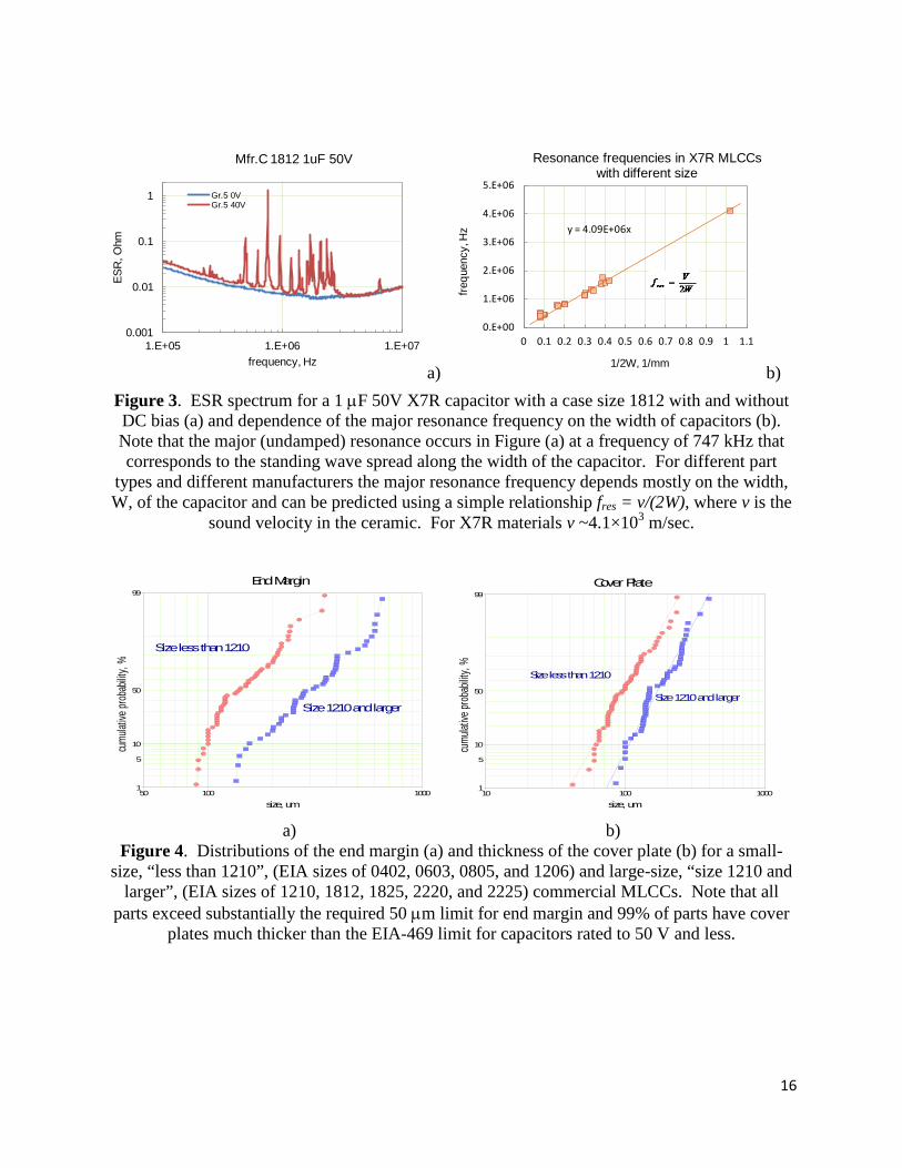
a) b) Figure 3. ESR spectrum for a 1 µF 50V X7R capacitor with a case size 1812 with and without DC bias (a) and dependence of the major resonance frequency on the width of capacitors (b). Note that the major (undamped) resonance occurs in Figure (a) at a frequency of 747 kHz that corresponds to the standing wave spread along the width of the capacitor. For different part
types and different manufacturers the major resonance frequency depends mostly on the width, W, of the capacitor and can be predicted using a simple relationship fres = v/(2W), where v is the
sound velocity in the ceramic. For X7R materials v ~4.1×10³ m/sec.
a) b)
Figure 4. Distributions of the end margin (a) and thickness of the cover plate (b) for a small-size, “less than 1210”, (EIA sizes of 0402, 0603, 0805, and 1206) and large-size, “size 1210 and
larger”, (EIA sizes of 1210, 1812, 1825, 2220, and 2225) commercial MLCCs. Note that all parts exceed substantially the required 50 µm limit for end margin and 99% of parts have cover
plates much thicker than the EIA-469 limit for capacitors rated to 50 V and less.
0.001
0.01
0.1
1
1.E+05 1.E+06 1.E+07
ESR
, Ohm
frequency, Hz
Mfr.C 1812 1uF 50V
Gr.5 0VGr.5 40V
y = 4.09E+06x
0.E+00
1.E+06
2.E+06
3.E+06
4.E+06
5.E+06
0 0.1 0.2 0.3 0.4 0.5 0.6 0.7 0.8 0.9 1 1.1
frequ
ency
, Hz
1/2W, 1/mm
Resonance frequencies in X7R MLCCs with different size
End Margin
size, um
cumu
lative
prob
abilit
y, %
50 10001001
5
10
50
99
Size 1210 and larger
Size less than 1210
Cover Plate
size, um
cumu
lative
prob
abilit
y, %
10 10001001
5
10
50
99
Size 1210 and larger
Size less than 1210

17
a) b) Figure 5. Relaxation of currents in 1 µF 50 V and 10 µF 50 V (a) and 3.3 µF 6.3 V (b)
capacitors at rated voltages. Currents that are decaying with time according to a power law, I = a×t-n, where a and n are constants, are due to the charge absorption (so-called Curie - von
Schweidler law). Absorption processes are intrinsic to the dielectric material used and can exceed currents caused by the presence of defects. Figure a) shows the reproducibility of
absorption currents in X7R capacitors and figure b) shows that measurements of currents within 120 seconds of electrification might not allow for discrimination between normal and cracked
capacitors.
Figure 6. Variations of normalized to VR breakdown voltages in different commercial X7R capacitors vs. rated voltage. Error bars correspond to standard deviations, and a solid line
corresponds to the requirements for the dielectric withstanding voltage (DWV) test. Note that breakdown voltages in low-voltage capacitors substantially, by factors from 4 to 40 exceed the
DWV requirements. Experiments show that VBR decreases in capacitors with structural damage, e.g. cracks, voids, delaminations; however, in majority of the cases VBR remains large
enough, so capacitors with defects have a low probability to be detected by the DWV testing.
I= a*t-0.9
I = a*t-0.7
1.E-10
1.E-09
1.E-08
1.E-07
1.E-06
20 200 2000
curr
ent,
A
time, sec
Absorption currents in X7R MLCCs
2220 Mfr.A 10uF 50V
2225 Mfr.B 1uF 50V
I = a*t-07
1.E-10
1.E-09
1.E-08
1.E-07
1.E-06
1.E+0 1.E+1 1.E+2 1.E+3 1.E+4
curr
ent,
A
time, sec
0805 Mfr.P X7R 3.3uF 6.3V
crack
normal
1
10
100
0 20 40 60 80 100 120
VBR
/VR
rated voltage, V
X7R MLCCs

18
Table A. Characteristics of dielectric materials in MLCCs per EIA 198
EIA class dielectric*
Dielectric class
Low Temp. rating, deg. C
High Temp rating, deg.C
Maximum Temp shift
Maximum loss of C,
% per decade hour **
C0G I -55 125 ± 30 ppm/ºC 0 X7R II -55 125 ± 15% 2.5 Y5V III -30 85 +22% -82% 7
* Explanations for dielectric codes are given in Table B below.
** When a class II or III ceramic capacitor is exposed to temperatures exceeding Curie point (typically between 120 °C and 130 °C), its capacitance value is maximum (C0) and then decreases with time of aging (t) according to an empirical logarithmic law:
)(log100
0 tC
CC×−=
− α , (2)
where α is a constant that indicates the rate of capacitance loss and is expressed as percent per decade of hours. For example, X7R capacitors right after soldering would have the maximum value of capacitance, but will lose 2.5% between 1 hr and 10 hr of aging, 5% between 1 hr and 100 hr, and 10% between 1 hr and 10000 hr of aging. The rate of capacitance loss is much greater for class III dielectrics than for class II. The effect is due to gradual changes in the domain structure of the dielectric and became negligible after a sufficient time of ageing. Equation (2) is not applicable at very short periods of time after exposure to high temperatures, but works reasonably well at t ≥ 1hr.
Table B. Temperature characteristic codes for class II and III dielectrics
Low Temp., deg.C Symbol
High Temp., deg.C
Symbol Max. capacitance change over temp
range, % Symbol
+10 Z +45 2 ±1 A -30 Y +65 4 ±1.5 B -55 X +85 5 ±2.2 C
+105 6 ±3.3 D +125 7 ±4.7 E +150 8 ±7.5 F +200 9 ±10 P ±15 R ±22 S +22 to -33 T +22 to -56 U +22 to -82 V
Examples. X7R: X=> -55C, 7=> +125C, R=> ±15%. Z5U: Z=> +10C, 5=> +85C, U=> +22% to -56%

19
Initial condition
Touch-up
Cracking upon cooling
Figure 7. Formation of cracks caused by touch-up with a soldering iron. Although large size (1210 and greater) capacitors are considered most vulnerable to thermal
stresses associated with manual soldering, a brief touch-up with a soldering iron to small-size parts (e.g.0402) with the purpose of improving a solder fillet can cause fracture in the capacitor. Small-size capacitors would heat up momentarily while the board might remain cold. Thermal
expansion of the capacitor (∆L) will be partially “frozen” upon solidification of solder thus creating tensile stresses and cracking in the part.
Solder
Board
Capacitor
Board
Capacitor
crackTensile stress
Board
CapacitorSolder
∆L