GUIDELINE FOR CHARACTERIZATION OF INTEGRATED CIRCUITSaecouncil.com/Documents/AEC_Q003A.pdf · AEC -...
21
AEC - Q003 Rev-A February 18, 2013 Component Technical Committee Automotive Electronics Council GUIDELINE FOR CHARACTERIZATION OF INTEGRATED CIRCUITS
Transcript of GUIDELINE FOR CHARACTERIZATION OF INTEGRATED CIRCUITSaecouncil.com/Documents/AEC_Q003A.pdf · AEC -...

AEC - Q003 Rev-A February 18, 2013
Component Technical CommitteeAutomotive Electronics Council
GUIDELINE FOR CHARACTERIZATION
OF INTEGRATED CIRCUITS

AEC - Q003 Rev-A February 18, 2013
Component Technical CommitteeAutomotive Electronics Council
Acknowledgment Any document involving a complex technology brings together experience and skills from many sources. The Automotive Electronics Counsel would especially like to recognize the following significant contributors to the development and release of this document: Characterization Sub-Committee Members: Tim Haifley Altera Sandra Healy Analog Devices Michael O’Sullivan Analog Devices Xin Miao Zhao [Q003 Team Leader] Cirrus Logic Ramon Aziz Delphi Corporation Paul Grosch Freescale Nick Lycoudes Freescale Laurie McTurk Freescale James Stanley Freescale Drew Hoffman Gentex Richard Lauks Infineon Harold Lorenz Infineon Jochen Roeder Infineon Tim Weyland Infineon Banjie Bautista ISSI Gary Fisher Johnson Controls Bob Knoell NXP Yizi Xing NXP David Ownby SMSC Joel Dobson Texas Instruments Thomas VanDamme TRW Daniel Chung Xilinx

AEC - Q003 Rev-A February 18, 2013
Component Technical CommitteeAutomotive Electronics Council
NOTICE
AEC documents contain material that has been prepared, reviewed, and approved through the AEC Technical Committee. AEC documents are designed to serve the automotive electronics industry through eliminating misunderstandings between manufacturers and purchasers, facilitating interchangeability and improvement of products, and assisting the purchaser in selecting and obtaining with minimum delay the proper product for use by those other than AEC members, whether the standard is to be used either domestically or internationally. AEC documents are adopted without regard to whether or not their adoption may involve patents or articles, materials, or processes. By such action AEC does not assume any liability to any patent owner, nor does it assume any obligation whatever to parties adopting the AEC documents. The information included in AEC documents represents a sound approach to product specification and application, principally from the automotive electronics system manufacturer viewpoint. No claims to be in conformance with this document shall be made unless all requirements stated in the document are met. Inquiries, comments, and suggestions relative to the content of this AEC document should be addressed to the AEC Technical Committee on the link http://www.aecouncil.com. Published by the Automotive Electronics Council. This document may be downloaded free of charge, however AEC retains the copyright on this material. By downloading this file, the individual agrees not to charge for or resell the resulting material. Printed in the U.S.A. All rights reserved Copyright © 2013 by the Automotive Electronics Council. This document may be freely reprinted with this copyright notice. This document cannot be changed without approval from the AEC Technical Committee.

AEC - Q003 Rev-A February 18, 2013
Component Technical CommitteeAutomotive Electronics Council
Page 1 of 18
GUIDELINE FOR THE CHARACTERIZATION OF INTEGRATED CIRCUITS
Text enhancements and differences made since the last revision of this document are shown as underlined text.
1. PURPOSE
The characterization of ICs is an extremely important function during the development of a new IC or the modification of an existing IC. The purpose of this document is to provide guidance by highlighting important considerations that should be evaluated during development of a characterization procedure. This document is not intended to be a specification on how to perform a characterization. To ensure consistent characterization every company should have a structured and documented characterization procedure. The characterization process should be used to ensure that the design and wafer fab/assembly processes being utilized demonstrate sufficient capability of providing a part that meets the requirements of the customer. The results of every characterization should be documented in a Characterization Report.
2. SCOPE
This guideline document provides the basis for establishing a procedure for characterizing the electrical performance of Integrated Circuit products. This characterization procedure should be used for new technologies, new wafer fabrication processes, new product designs, and change in bill of material, manufacturing location and significantly modified ICs. This full scale characterization is a procedure to assess a new product line, including establishing supplier datasheet limits. For qualification of a product with established supplier datasheet limits, please reference AEC-Q100-009 Electrical Distributions Assessment procedure.
3. DEFINITIONS 3.1 ANOVA
Analysis of variance between groups. 3.2 Characterization
The process of determining the fundamental electrical and physical characteristics of a device based on statistical analysis of experimental data modeling. The input is batches of newly manufactured integrated circuit parts subjected to characterization sampling and the output is a data set. The result is to prove or disprove that the devices can and will continue to perform their targeted functions according to the product definition. Data resulted from characterization are used to specify datasheet limits and functions. It is important to determine the ESD and Latch-up capability of a part early in the development cycle as these parameters could have a significant impact on the performance of the part.

AEC - Q003 Rev-A February 18, 2013
Component Technical CommitteeAutomotive Electronics Council
Page 2 of 18
3.3 Cpk
A measure of the relationship between the specification limits and the capability. Reference: PPAP Manual Fourth Edition, see SPC Manual.
3.4 Criteria for Characterization
A device that meets the following criteria should be considered a candidate for characterization. These criteria should not be considered a limitation, but a starting point for factors to consider. • New product design. • New device layout or changes to an existing device that could impact electrical parameters. • New cell structure(s) which have not been used in production components. • New processing methods or materials. • New operating bias condition requirements (re-characterize at new bias extremes). • New operating environmental conditions (such as voltage and temperatures).
3.5 Device Electrical Parameters
Electrical parameters specified in the part specification for the device. 3.6 Guardband
The difference between limits used for screening (e.g., characterization, production testing, etc.) and specification limits. Guardbands are used to account for repeatability and reproducibility issues.
3.7 LSL
Lower Specification Limit. 3.8 Matrix Lot
Matrix lot is a lot composed of wafers that are based on manufacturing site’s process of records and manufactured to the process corners for identifying design/process weakness and improvement as well as indicating yield sensitivity corners.
3.9 PPM
Part Per Million. In this document the PPM is the probability the parameter will be outside of product specification limits.
3.10 Specification Limits (e.g., Data Sheet Limits)
Numerical values of maximum, minimum, and typical for electrical parameters specified in supplier’s data sheet or customer’s part specification. These values are used to determine pass/fail criteria for device characterization and production testing.

AEC - Q003 Rev-A February 18, 2013
Component Technical CommitteeAutomotive Electronics Council
Page 3 of 18
3.11 Standard Deviation
Standard deviation or sigma is a measure of how widely values are dispersed from the average value (the mean).
3.12 USL
Upper Specification Limit. 4. CHARACTERIZATION PROCEDURE
An outline of factors that should be considered when establishing a characterization procedure is provided here for every supplier to establish a characterization procedure. The Device Characterization Process Flow is shown in Figure 1.
4.1 Device Characterization Plan
The characterization plan should include the following major activities for the device to be characterized: • Review the Characterization Checklist, see Appendix 1. • Determination of if a matrix lot is necessary for the device characterization. • Determination of the characterization method to be used. • Establishment of the parameters and conditions to be characterized. • Define format of the characterization report.
4.2.1 Matrix Lot Characterization
When characterizing a matrix lot, the number of split cells, samples per cell and the data analysis methods should also be defined in the plan. Guidelines for designing, planning and analyzing the split cells for a matrix lot are provided in Appendix 2 and 3.
4.2.2 Sample Sizes
When deciding on sample sizes for characterization, two important factors are to be considered: confidence interval and confidence level. Please see details in Appendix 4 for help in determining sample sizes.
4.3 Characterization Report
The characterization report should include the following: a. A copy of the characterization plan. b. A detailed discussion of the characterization methods used (see Appendix 1, 2, 4 and 5). c. A listing of parameters and conditions used in characterization. d. Characterization data analysis and conclusions. e. Document simulation results including brief explanations on methods applied – for
parameters that are not measurable and/or tested in production and covered by design simulation only.
f. Identify part weaknesses and reliability concerns and define corrective actions.

AEC - Q003 Rev-A February 18, 2013
Component Technical CommitteeAutomotive Electronics Council
Page 4 of 18
Product 1234
IsCharacterization
Required?
New productNew chip layout or changes to an existingNew cell structureNew processing methods or materialsNew operating bias conditionrequirements
PerformCharacterization
CharacterizationReport
Approve bySimilarity
Internal CharacterizationProcedure
Completion of Project
Review CharacterizationChecklistDetermination of thecharacterization methodEstablishment of theparameters & conditions
Characterization methodsParameters & conditionsData analysis & conclusionsSimulation resultsPart weaknesses & reliabilityconcerns
Characterization Plan
Yes
No
Yes
No
Approve Report?
Modify Plan
Figure 1: Characterization Flowchart

AEC - Q003 Rev-A February 18, 2013
Component Technical CommitteeAutomotive Electronics Council
Page 5 of 18
4.4 Characterization Data Analysis
There are many statistical methods that could be used to perform analysis of the data. One commonly accepted is using Cpk when the output response could be assumed with a normal or Gaussian distribution.
4.4.1 Cpk and PPM to Data Sheet Limits
Cpk computes the differentiation between the actual process average and the specification limit over standard deviation. The two things which Cpk measures: a. The interpretations of the mean as how close they are to the center of the upper and lower
spec limits? b. How extensively the readings are spread over the measurement range? The distance of the upper and the lower spec from the distribution mean on the basis of the Cpk value could be expressed in multiples of the standard deviation. In the absence of production test to screen out parts outside specifications, the Cpk of the specification limits will give an indication of the expected ship PPM. Both short term and long term Cpk can be considered.
4.4.1.1 Short Term Cpk in Relation to PPM
In quality control terms, PPM stands for the number of parts per million indicated by this fraction of area. In a short term sense, a process could have a centered normal distribution with two sided specification (Upper Spec Limit / Lower Spec Limit) and no sigma shift, the relation between Cpk and PPM is as shown in Figure 2.
Figure 2: Cpk vs. Probability of parts outside of specification (centered symmetrical normal distribution)
With this assumption, a Cpk value of 1.00 means that 2700 PPM (0.27%) of the manufactured parts could be out of tolerance, while Cpk 1.67 means that 0.57 PPM (0.000057%) are potential rejects. Examples of typical Cpk and PPM values are given in Table 1 for a parameter with min and max specifications.

AEC - Q003 Rev-A February 18, 2013
Component Technical CommitteeAutomotive Electronics Council
Page 6 of 18
Table 1: Short Term CPK and PPM Estimation
Cpk Sigma PPM 0.67 2.00 45500 1.00 3.00 2700 1.33 4.00 63 1.67 5.00 0.57 2.00 6.00 0.002
4.4.1.2 Long Term Cpk in Relation to PPM
In most product manufacturing the process does shift. The relation between Cpk and PPM allowing for a 1.5 sigma process shift over time is illustrated in Figure 3.
Figure 3: Probability of parts outside of specification for Cpk of 1.67 (left) and with 1.5 Sigma shift toward USL and LSL (right)
With this 1.5 Sigma shift, the potential parts outside specification could become significant higher compared to without shift. Examples of typical Cpk and PPM values with long term 1.5 Sigma shift are given in Table 2. For comparison purposes, Cpk and Sigma values exclude shift are included. Under this condition, a Cpk of 1.67 may deteriorate to a Cpk of 1.16 which will result in a 233 PPM compared to 0.57 PPM from Table 1.
Table 2: CPK and PPM Estimation (with a 1.5 Sigma process drift)
Short term Assuming a long term 1.5 sigma shift
Cpk Sigma Sigma with shift
Cpk with shift PPM
0.67 2.00 0.50 0.17 308,538 1.00 3.00 1.50 0.50 66,807 1.33 4.00 2.50 0.83 6,210 1.67 5.00 3.50 1.17 233 2.00 6.00 4.50 1.50 3
AEC - Q003 Rev-A February 18, 2013
Component Technical CommitteeAutomotive Electronics Council
Page 7 of 18
4.4.2 Cpk and PPM with Production Test
To maintain low PPM when the Cpk to datasheet limits is inside six sigma (Cpk<2.0), 100% production test should be considered to screen out parts that are outside specification. Because of test measurement error and parametric temperature and lifetime drift, appropriate statistical models should be used to create test limits that guardband against datasheet limits to ensure the shipped product meets the customer PPM requirement.
4.4.3 Acceptance Guidelines
Cpk is a typical measure of characterization data for acceptance. The acceptance value of Cpk should be target PPM level dependent with the process deviation (sigma) from target process during production should be taken into consideration as well. Please reference AEC Q100 and other supplier and customer agreement for acceptable Cpk values.
4.5 Data Reporting
Characterization data reporting is an important part of the final report. A summary of the data should be provided and raw data should be archived and available for customer review upon request. Graphical presentation of the statistical analysis of the experimental data and modeling is strongly encouraged. For significant changes made to existing devices, comparison of data from the new revision to the previous revision is recommended. The data could be presented in different ways with two examples Correlation plot (Figure 4) or box plot (Figure 5) given below. Other methods such as histograms, cumulative plots, and raw data plots are often used as well.
4.5.1 Hyper–Ellipsoid Correlation Plot
This includes the distribution of an electrical parameter as a function of other parameter(s) variation. The graphical presentation of the characterization for a typical electrical parameter is a multivariate hyper-ellipsoid, see Figure 4 (frequently called a Correlation Plot).
Test Limit
Each dot is ameasurementfrom one part
SpecificationLimit
Guardband
Parameter 1
Para
met
er 2
Figure 4: Correlation Plot

AEC - Q003 Rev-A February 18, 2013
Component Technical CommitteeAutomotive Electronics Council
Page 8 of 18
4.5.2 Box Plot
This includes the distribution of an electrical parameter as a function of operating condition variations (voltage, temperature, frequency, pad load conditions, input timings) or across process window matrix cells. The graphical presentation of the characterization results for an electrical parameter in relation to multiple operating conditions could be presented in different ways such as Correlation plot (Figure 4) or box plot (Figure 5). Statistical data from device characterization (e.g., target sample size, min, mean, median, max, sigma / cpk (nominal group)) should be provided in addition for each box plot.
Group X Group Y Group Z Group Q
Par
amet
er
Group / Operating Condition Variations
25th Percentile
Minimum
Mean
50th Percentile
Maximum
75th Percentile
Lower Spec Limit
Upper Spec Limit
Figure 5 – Box Plot 5. APPROVAL AND ACCEPTANCE
The characterization report should be approved by a responsible supplier representative. The results of the characterization should be shared with the customer per request (this sharing may include a copy of the characterization report or selected portions of the characterization report).

AEC - Q003 Rev-A February 18, 2013
Component Technical CommitteeAutomotive Electronics Council
Page 9 of 18
APPENDIX 1: CHARACTERIZATION CHECKLIST A1.1 The following points should be evaluated during the planning stage for product characterization:
• Have all the cell structures used in this product been characterized? • Has the wafer fab process changed since the cell structure characterizations? • If the wafer fab process has changed, do the simulation models that will be used for
characterization account for all wafer fab process changes? • If matrix devices will be needed, which process windows should be involved in the matrix?
What is the worst case variation in these process windows? (Note: The worst case processing variation should be based on the worst case conditions observed during the last six months or expected during normal manufacturing.) Who should participate in making these decisions?
• Are there matrix cell interactions that should be considered? • How can simulation models be used to simplify and expedite the characterization process?
How good are the available simulation models? What is the confidence in the simulation models? What are the risks if the available simulation models are used?
• Have the drift characteristics of the cell structures been characterized? Is a device parameter
drift analysis needed as part of this characterization? • Are there stresses associated with the product package that could affect the initial and late
life electrical parameters of the product? • If matrix units are required, how many (sample size) from each matrix cell? How many
process variations need to be characterized? Will the product be characterized beyond the required part specification requirements (hotter or colder temperatures, higher or lower frequencies, higher or lower bias voltages)? Will the software required for the characterization be available when needed?
• Do we know the junction temperatures (hot and cold) that must be evaluated in this
characterization? Have the thermal characteristics of the measurement system(s) been considered, see Appendix 5?
• What form will matrix devices be in for the characterization – packaged? wafer level? Have
packaging requirements been included in the characterization plan? • Will the ESD and Latch-up capability be evaluated early in the development cycle?

AEC - Q003 Rev-A February 18, 2013
Component Technical CommitteeAutomotive Electronics Council
Page 10 of 18
APPENDIX 2: MATRIX LOT CHARACTERIZATIONS A2. For a new device, in particular in a new technology/process, a cross-factored experiment called a
Matrix Lot should be prescribed to estimate the effect of long-term process drifting. The Matrix Lot design should be chosen to maximize the estimation of all desired factors and their interactions. The center value run of the Matrix Lot is called the nominal split. The other cells are called corner cells or splits. Characterization data measured on parts taken from different cells of the matrix lot will have different values. Each part parameter, then, will have a performance range, the result of parts being tested from different cells of the matrix in conjunction with matrix cells are displayed in Figure 2.1.
Figure A2.1: Typical Matrix Cells (top) and Parameter Performance Range (bottom) A2.1 Various Methods for Matrix Lot/Process Characterization
The performance of the Matrix lot could be evaluated using Cpk but with expected values that are different for corner cells from nominal. The Cpk assessment criteria limits for process corner cells should be based on the range of applied process shift and therefore a de-rating factor shall be applied to reflect the long term probability of the process running at this condition.
A2.2 Characterization Statistical Model
To understand the performance characteristics of the Matrix Lot, a statistical model is built. The location parameter and variances associated with that model will be estimated. These estimates will be used to assess the process capability over time. This assessment is often in the format of a Cpk calculation and the model is built using Analysis of Variance techniques (ANOVA). Several examples of statistical models for analyzing the data are provided here.
AEC - Q003 Rev-A February 18, 2013
Component Technical CommitteeAutomotive Electronics Council
Page 11 of 18
A2.2.1 Cell Means Model
Could be used when corner cell states are assumed to be stable states into which the process may drift over time and will stay there unless adjusted back. Cell means model is a one-way ANOVA and it assumes homogeneous variance across all cells. CPK and a 95% confidence interval on CPK could be estimated from the cell means model. Here focus is on the worst performing cell, based on its CPK. It uses the worst corner cell performance as an indicator. If it stays within specifications, then the process overall will. In the case the variance is not homogeneous across cells; the data from each cell should be analyzed separately. The CPK from each cell should be evaluated against chosen CPK criteria.
A2.2.2 Mixed Model
Could be used when corner cell states are interpreted as unstable states among which the process will drift into over the long term. Mixed model ANOVA uses more than one variance component. There is the variance within the cells and the variance from cell to cell. Each of these two is modeled as a random effect within the mixed model. If that is your company’s interpretation, it might be good to get your professional statistician involved when building the models.
A2.2.3 Random Effects Linear Model
Uses ANOVA to estimate the variation within the lots, and between the lots, and the total variance is the sum of these two. This has general application for analysis of data when multiple lots and/or matrix lots are included.
A2.2.4 Other Possible Models
There are other possible statistical models that may be more appropriate than the ones suggested here. The statisticians in your company may have ideas much more mathematically involved than those suggested in this document.

AEC - Q003 Rev-A February 18, 2013
Component Technical CommitteeAutomotive Electronics Council
Page 12 of 18
APPENDIX 3: DESIGN INDEX A3. The idea of representing the goodness or badness of a product's Device Parameter performance
(over the worst case expected variation in Key Fab Process limits) with a single value is the reason for establishing a Design Index (DI). A Design Index of 1 or greater for a particular parameter requirement means that the device meets that parameter requirement at all matrix points. (Note: A Design Index of less than 1 indicates that a particular parameter will probably cause a higher yield loss during normal production.) This section will discuss the theory behind the DI and how to use it.
A3.1 In a matrix characterization (or simulation), processing variables are forced to certain values (to form
matrix cells) and the product performance is evaluated. The goal of the characterization is to determine if the device performance will stay within specification limits when processing variables are forced to their worst case values, see Appendix 1. The Device Parameters are the values measured (or modeled), or tests performed, to ensure that the device meets all of the electrical requirements defined in the Part Specification. In general, the Device Parameters measured on parts taken from different cells of the matrix will have different values. Each part parameter, then, will have a performance range, the result of parts being tested from different cells of the matrix.
A3.2 In defining the DI it is assumed that the Device Parameter population that is sampled in each matrix
cell is normally distributed and independently distributed. The index also assumes that the product would yield equally well when processed at any point within the Design/Process window. Thus, there is no weighting of the matrix data. The actual definition of DI is very similar to that of the Cpk index. The important difference is that the Cpk is based on a single normal distribution (grouping all matrix cells into one distribution) while the DI is based on the worst case of several individual matrix distributions, see Figure A3.1.
Figure A3.1: Comparison of Cpk and Design Index
See Figure A3.2 for definition of WL, WU

AEC - Q003 Rev-A February 18, 2013
Component Technical CommitteeAutomotive Electronics Council
Page 13 of 18
A3.3 The DI (one number for each Device Parameter upper and lower specification limit) is determined as follows: a. Statistically analyze the electrical distribution characteristics for each matrix cell, device
parameter, and test temperature. (The statistical analysis should include an estimation of the mean and the worst case edges for each distribution, and should be based on the confidence interval (ci) on the estimated mean, see Figure A3.2.) For example, if there are 5 matrix cells (as shown in Figure A2.1) and three test temperatures, there will be 15 distributions (5 at each temperature) for each Device Parameter, see Figure A3.3.
b. Using the Extreme WL (A) and Extreme WU (B), as shown in Figure A3.3, calculate the mean
[M = (A + B) / 2]. c. Then, determine the DI values (DI lower and DI upper) for each parameter) as shown in
Figure A3.3.
Figure A3.2: Statistical Analysis, Including the Confidence Interval
AEC - Q003 Rev-A February 18, 2013
Component Technical CommitteeAutomotive Electronics Council
Page 14 of 18
Figure A3.3: Analysis of Five Matrix Cells at Three Temperatures
AEC - Q003 Rev-A February 18, 2013
Component Technical CommitteeAutomotive Electronics Council
Page 15 of 18
APPENDIX 4: TEST DEVICE AND SAMPLE SELECTION A4. Test Device Selection
One goal of characterization is to discover potential problems during early development when changes can be made quickly, easily, and less expensively. Therefore, caution should be exercised so that pretesting before characterization is minimized, since it has the possibility of truncating the normal matrix cell distribution and hiding potential problems.
A4.1 One approach is to pre-test to only eliminate non-functional devices from the characterization sample. Example: to help define non-functional, the following would be considered test limits for functional devices:
• Override specification required parametric failures and only perform relaxed spec functional tests.
• Widen all specification required parametric limits by a significant digit. A4.2 A second method for sample population selection is the following. The data should be pre-screened
to remove statistical outliers before processing. One suitable method is using box-plot Inter Quartile Range (IQR) to generate outlier ‘fences’. The inter quartile range can be calculated by ordering the data in ascending order, and taking the delta between the 25th percentile point (called the first quartile Q1) and the 75th percentile point (called the third quartile Q3). The IQR is the delta between Q1 and Q3. The outlier fences are then set to:
Lower fence = Q1 – 3* IQR Upper fence = Q3 + 3* IQR
Any data-points that fall outside these fences can be removed for calculating the mean and sigma of the population.
A4.3 The method of selecting device can have a large effect on the amount of inherent process variation
that is included in the data. The main concern is to understand and design for the largest sources of inherent process variation. Due to the number of different process technologies it is the responsibility of the supplier to develop a combination of lots, wafers, and device locations that will provide the inherent process variation. A thorough analysis of sample size should also consider the following:
• Which wafers are selected for a cell? • Which device locations are selected on a wafer?
A4.4 Sample Size Selection and Margin Error
During characterization, random samples are chosen. The measured results deviate in the mean and limit ranges from the population Normal Distribution depending on the parts sampled. Larger sample sizes will help to reduce such deviation/error. Two important factors are to be considered when deciding on sample sizes for characterization.
A4.4.1 The confidence interval which is also called margin of error. When a measurement is taken on a
parameter on the samples, one could use a confidence interval to state that the measurement from the entire relevant population will be between the mean minus the interval and the mean plus the interval.
A4.4.2 The confidence level tells how sure one could be. It represents how often the true measurement
lies within the confidence interval. A 95% confidence level, a value used as customary, means one could be 95% certain.
AEC - Q003 Rev-A February 18, 2013
Component Technical CommitteeAutomotive Electronics Council
Page 16 of 18
A4.4.3 If the data conforms to the normal distribution, the two-tailed confidence interval may be calculated
using the following equation:
Lower confidence bound = - 1.96 s / √n Upper confidence bound = + 1.96 s / √n Where: = mean value of sample
s = standard deviation n = (random) sample size 1.96 corresponding to 95% confidence level of Normal Distribution
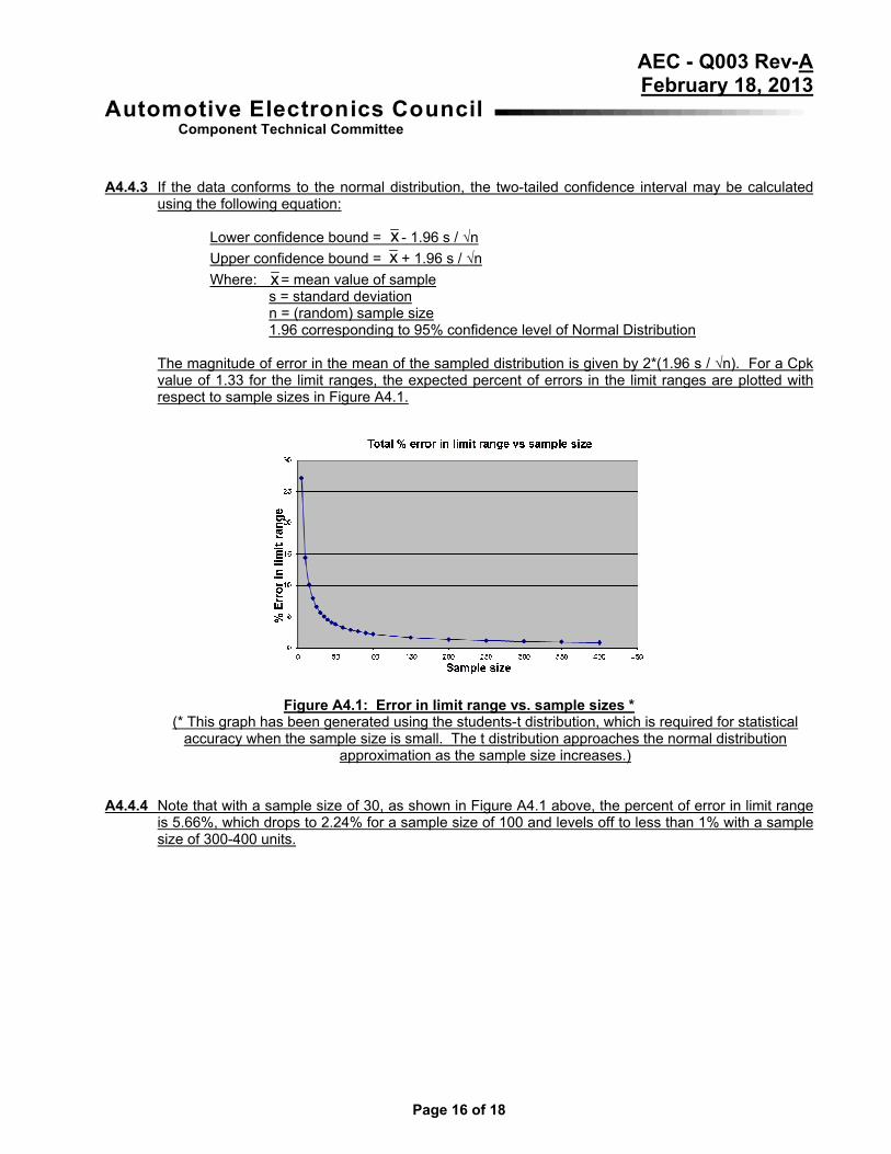
The magnitude of error in the mean of the sampled distribution is given by 2*(1.96 s / √n). For a Cpk value of 1.33 for the limit ranges, the expected percent of errors in the limit ranges are plotted with respect to sample sizes in Figure A4.1.
Figure A4.1: Error in limit range vs. sample sizes * (* This graph has been generated using the students-t distribution, which is required for statistical
accuracy when the sample size is small. The t distribution approaches the normal distribution approximation as the sample size increases.)
A4.4.4 Note that with a sample size of 30, as shown in Figure A4.1 above, the percent of error in limit range is 5.66%, which drops to 2.24% for a sample size of 100 and levels off to less than 1% with a sample size of 300-400 units.
xx
x

AEC - Q003 Rev-A February 18, 2013
Component Technical CommitteeAutomotive Electronics Council
Page 17 of 18
APPENDIX 5: CHARACTERIZATION TESTING A5. The device selected for characterization shall be tri-temperature tested. Test temperatures need to
be established for room, hot, and cold test. The test setup temperature extremes should be able to duplicate worst case product application junction temperatures. It should be stressed that the junction temperature of the device in the selected operating condition is the actual characterization target. For example, a low test temperature limit of -55ºC might be required for a -40ºC instantaneous customer need (i.e. operate on cold wake-up) to account for a 15ºC steady state heating during testing. Likewise, a high test temperature limit of 135ºC might be required for a 150ºC instantaneous package test to account for a 15ºC steady state heating during testing. The bias conditions and subsequent power consumption will determine if there is sufficient energy dissipation to necessitate the need for test temperature correction(s). In some situations an instantaneous condition is assumed that would null the effects of thermal dissipation, while in other conditions a high energy steady-state condition is assumed that would necessitate the use of temperature correction(s). Simulate a Customer Junction Temperature of 155ºC If the starting temperature of a customer system is: ...................................................................... 125ºC And a thermal gradient (w/bias condition) causes a
temperature increase of: ..................................................................................................... 30ºC Then the customer junction temperature requirement
is: ...................................................................................................................................... 155ºC Characterization Test Temperature The junction temperature to simulate is: ........................................................................................ 155ºC If the steady state heating during testing causes a
thermal gradient (w/bias condition) that results in a temperature increase of: ................................................................................... 15ºC
Then the required final test setup (Characterization test) temperature is: ........................................................................... 140ºC *
* Note: Additional temperature may be added to this value for guardbanding.

AEC - Q003 Rev-A February 18, 2013
Component Technical CommitteeAutomotive Electronics Council
Page 18 of 18
Revision History
Rev # -
A
Date of change
July 31, 1997
Feb. 18, 2013
Brief summary listing affected sections Initial Release. Complete Revision. Revised Acknowledgement and Sections 2, 3.2, 3.4, 3.5, 3.10, 4, 4.1, 4.2, 4.3, and Appendix 1 through 5. Added Notice Statement; new Sections 3.1, 3.3, 3.7 to 3.12, 4.2.1, 4.2.2, 4.4, 4.4.1, 4.4.1.1, 4.4.1.2, 4.4.2, 4.4.3, 4.5, 4.5.4, 4.5.2, and 5; new Figures 1, 2, 3, 4, 5, and A4.1; and new Tables 1 and 2. Deleted signature block.