Gto
53
Engr. Affifa Adeeb The Islamia University of Bahawalpur University College of Engineering & Technology EEN-324 EEN-324 Power Electronics Power Electronics Thyristor Devices Thyristor Devices Silicon Controlled Silicon Controlled Rectifiers (SCR) Rectifiers (SCR) 1
-
Upload
rameshbabu -
Category
Documents
-
view
219 -
download
1
description
notes
Transcript of Gto
Engr. Affifa Adeeb
The Islamia University of BahawalpurUniversity College of Engineering &
Technology
EEN-324EEN-324Power ElectronicsPower Electronics
Thyristor DevicesThyristor DevicesSilicon Controlled Rectifiers Silicon Controlled Rectifiers
(SCR)(SCR)
1
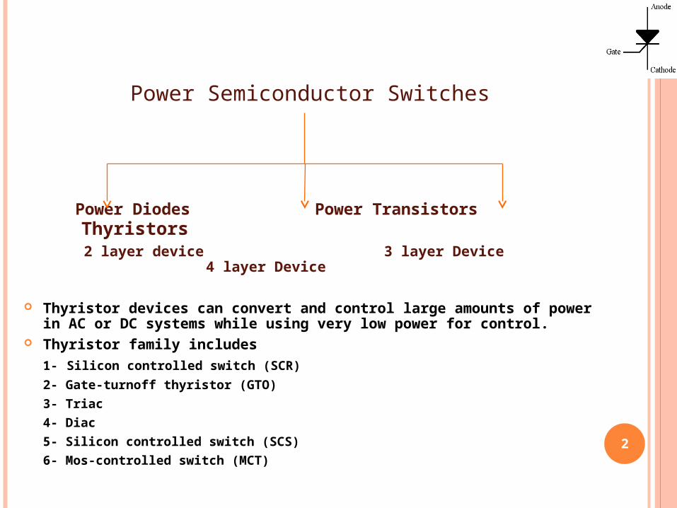
Power Semiconductor Switches
Power Diodes Power Transistors Thyristors
2 layer device 3 layer Device 4 layer Device
Thyristor devices can convert and control large amounts of power in AC or DC systems while using very low power for control.
Thyristor family includes1- Silicon controlled switch (SCR)
2- Gate-turnoff thyristor (GTO)
3- Triac
4- Diac
5- Silicon controlled switch (SCS)
6- Mos-controlled switch (MCT)
2

INTRODUCTION SCR is most popular of thyristor family due to its
Fast switching action , small size and high voltage and current ratings.
It is commonly used in power electronic applications.
SCR has 3 terminals (gate provides control)
SCR is turned on by applying +ve gate signal
when anode is +ve with repect to cathode.
SCR is turned off by interrupting anode
current.
3
PNPN structure Symbol

TWO TRANSISTOR MODEL OF SCR
4
Gate requires small positive pulse for short duration to turn SCR on. Once the device is on, the gate signal serves no useful purpose and can be removed.
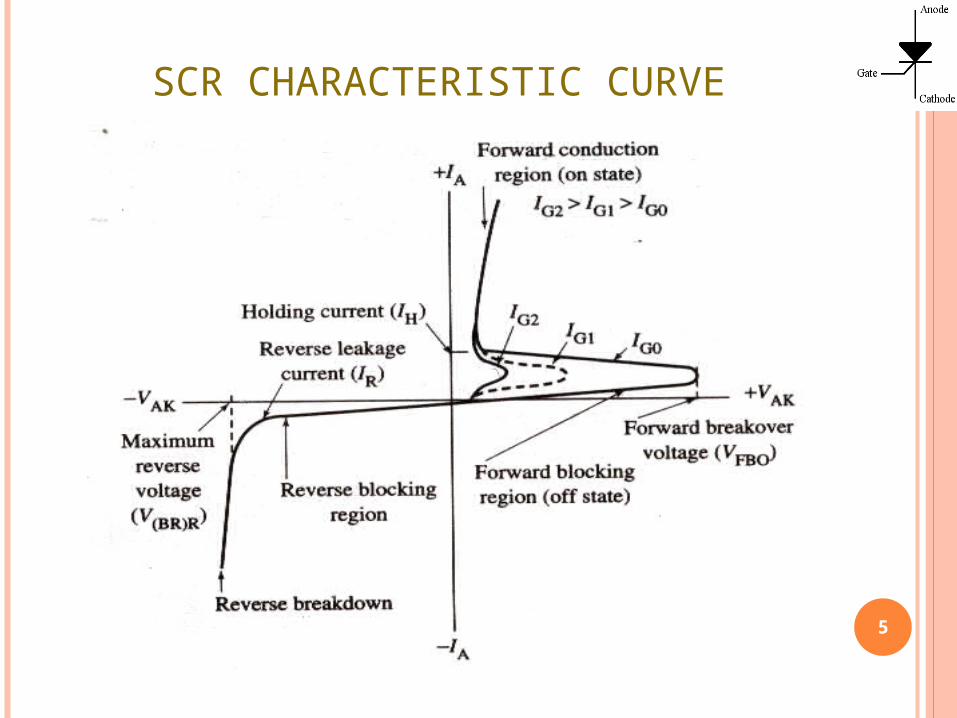
SCR CHARACTERISTIC CURVE
5

IDEAL CHARACTERISTIC OF SCR
6
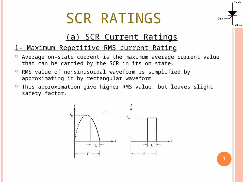
SCR RATINGS(a) SCR Current Ratings
1- Maximum Repetitive RMS current Rating Average on-state current is the maximum average current value that can be
carried by the SCR in its on state. RMS value of nonsinusoidal waveform is simplified by approximating it by
rectangular waveform. This approximation give higher RMS value, but leaves slight safety factor.
7
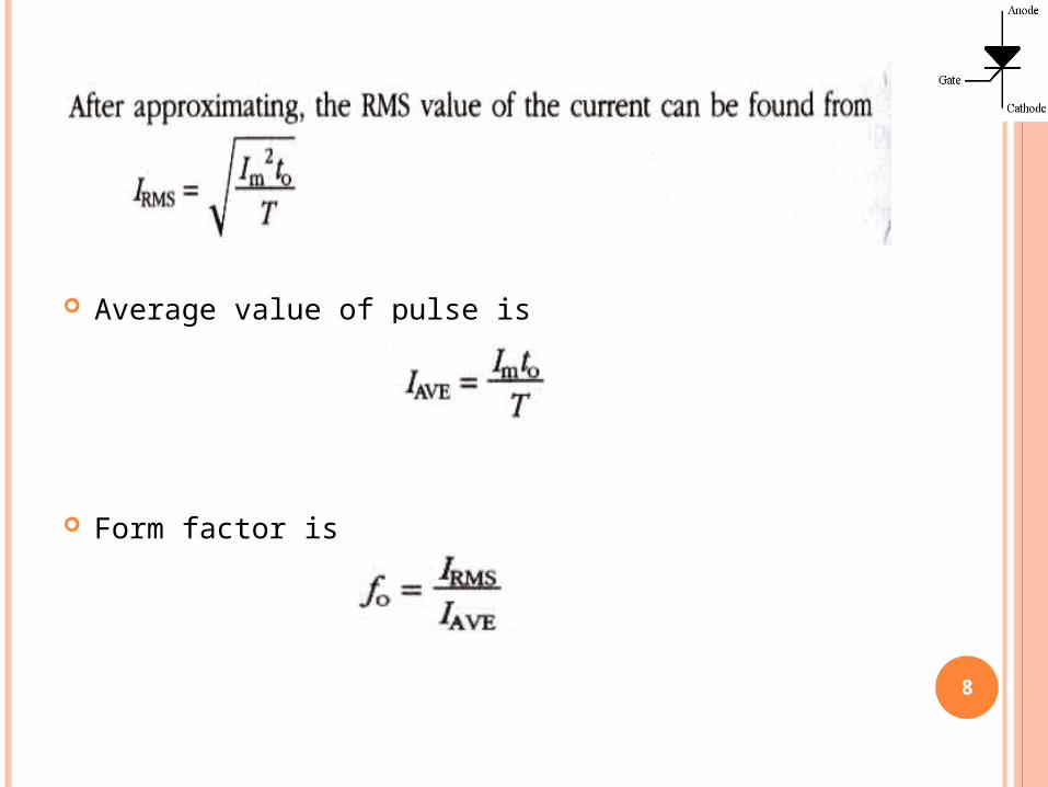
8
Average value of pulse is
Form factor is

Knowing the form factor for given waveform, RMS current can be obtained from
IRMS=fo(IAVE) Maximum repetitive RMS current is given by
IT(RMS)=fo(IT(AVE)) Conduction angle verses form factor
9
Conduction angle (θ)
Form factor (fo)
20° 5.0
40° 3.5
60° 2.7
80° 2.3
100° 2.0
120° 1.8
140° 1.6
160° 1.4
180° 1.3
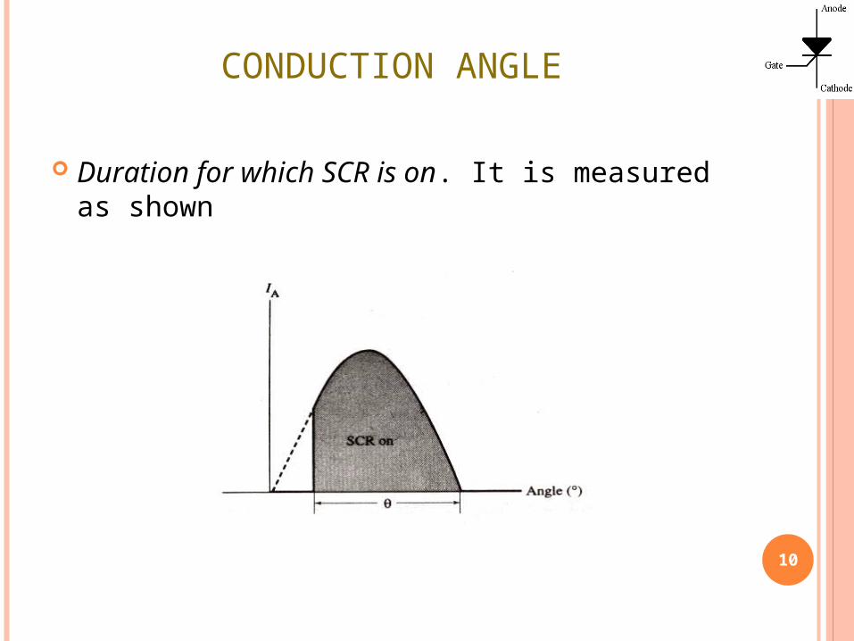
CONDUCTION ANGLE
10
Duration for which SCR is on. It is measured as shown

2- Surge Current RatingPeak anode current that SCR can handle for brief duration.
3- Latching currentMinimum anode current that must flow through the SCR in order for it to stay on initially after gate signal is removed.
4- Holding CurrentMinimum value of anode current, required to maintain SCR in conducting state.
11
(B) SCR VOLTAGE RATINGS
1- Peak repetitive forward blocking voltageMaximum instantaneous voltage that SCR can block in forward direction.
2- Peak Repetitive Reverse VoltageMaximum instantaneous voltage that SCR can withstand, without breakdown, in reverse direction.
3- Non-repetitive peak reverse voltage Maximum transient reverse voltage that SCR can withstand.
12
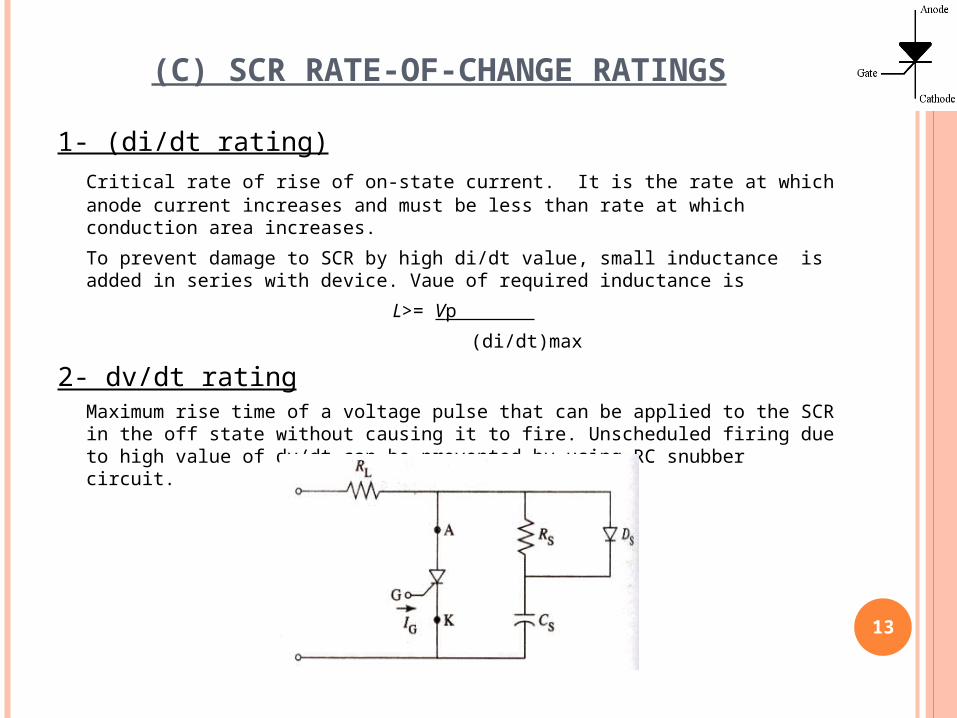
(C) SCR RATE-OF-CHANGE RATINGS
1- (di/dt rating)Critical rate of rise of on-state current. It is the rate at which anode current increases and must be less than rate at which conduction area increases.
To prevent damage to SCR by high di/dt value, small inductance is added in series with device. Vaue of required inductance is
L>= Vp
(di/dt)max
2- dv/dt ratingMaximum rise time of a voltage pulse that can be applied to the SCR in the off state without causing it to fire. Unscheduled firing due to high value of dv/dt can be prevented by using RC snubber circuit.
13
(D) GATE PARAMETERS
1- Maximum Gate Peak Inverse VoltageMaximum value of negative DC voltage that can be applied without damaging the gate-cathode junction.
2-Maximum Gate Trigger CurrentMaximum DC gate current allowed to turn on the device.
3- Maximum gate trigger voltageDC voltage necessary to produce maximum gate trigger current.
4- Maximum Gate Power DissipationMaximum instantaneous product of gate current and gate voltage that can exist during forward-bias.
5- Minimum gate trigger voltageMinimum DC gate-to-cathode voltage required to trigger the SCR.
6-Minimum gate trigger currentMinimum DC gate current necessary to turn SCR on.
14
15
Series and Parallel Series and Parallel SCR ConnectionsSCR Connections
SCRs are connected in series and parallel to extend voltage and current ratings.
For high-voltage, high-current applications, series-parallel combinations of SCRs are
used.
16

SCRS IN SERIES
Unequal distribution of voltage across two series SCRs.
Two SCRs do not share the same supply voltage. Maximum voltage that SCRs can block is V1+V2, not 2VBO. 17
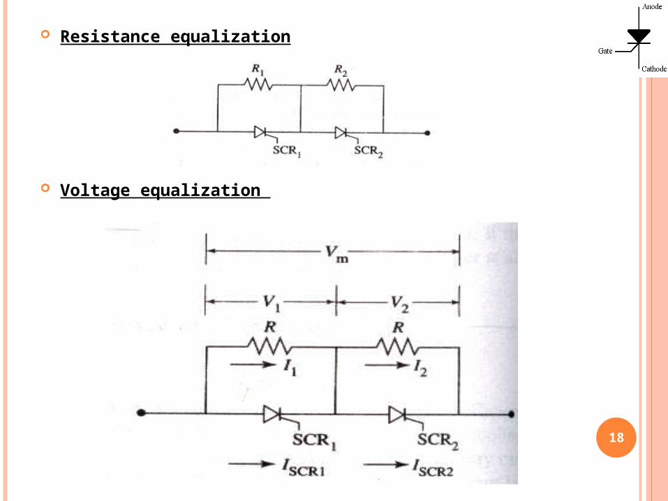
Resistance equalization
Voltage equalization
18
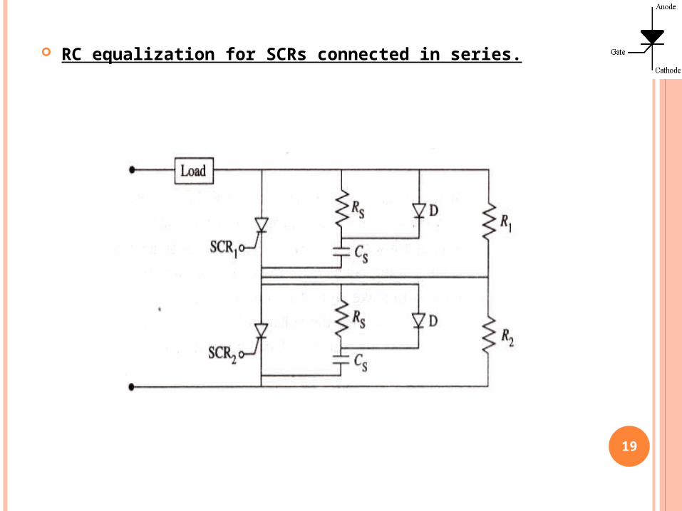
RC equalization for SCRs connected in series.
19

SCRS IN PARALLEL Unequal current sharing between two SCRs is shown:
Total rated current of parallel connection is I1+I2, not 2I2.
20

With unmatched SCRs, equal current sharing is achieved by adding low value resistor or inductor in series with each SCR, as shown below.
Value of resistance R is obtained from:
R=V1-V2
I2-I121
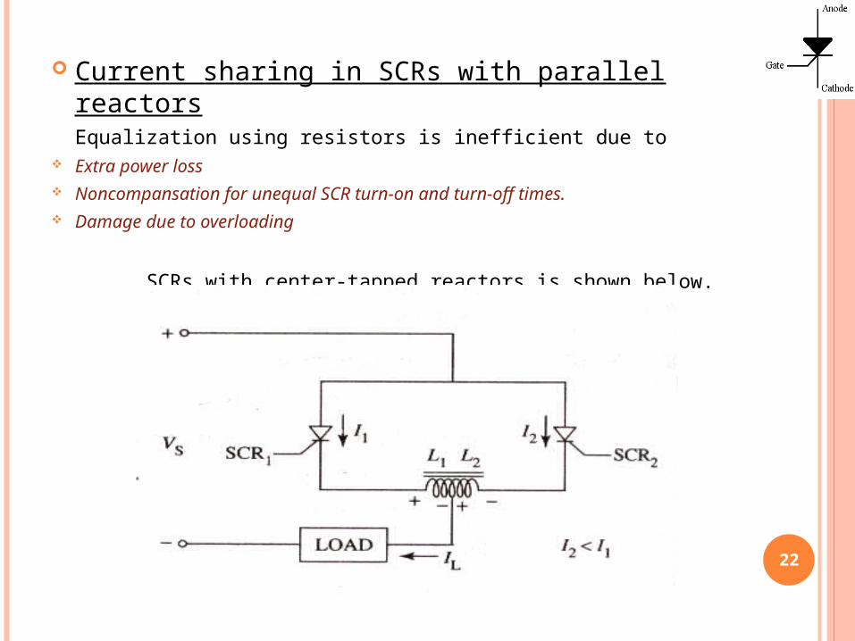
Current sharing in SCRs with parallel reactorsEqualization using resistors is inefficient due to
Extra power loss Noncompansation for unequal SCR turn-on and turn-off times. Damage due to overloading
SCRs with center-tapped reactors is shown below.
22

23
SCR Gate-Triggering SCR Gate-Triggering CircuitsCircuits
Triggering circuits provide firing signal to turn on the SCR at precisely the correct time.
Firing circuits must have following properties1. Produce gate signal of suitable magnitude and
sufficiently short rise time.
2. Produce gate signal of adequate duration.
3. Provide accurate firing control over the required range.
4. Ensure that triggering does not occur from false signals or noise
5. In AC applications, ensure that the gate signal is applied when the SCR is forward-biased
6. In three-phase circuits, provide gate pulses that are 120° apart with respect to the reference point
7. Ensure simultaneous triggering of SCRs connected in series or in parallel.
24

TYPES OF GATE FIRING SIGNALS
1. DC signals2. Pulse signals3. AC signals
25
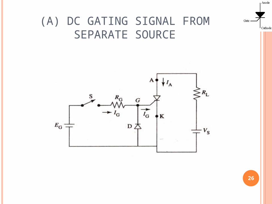
(A) DC GATING SIGNAL FROM SEPARATE SOURCE
26
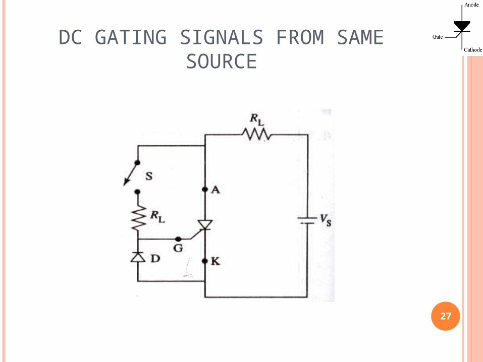
DC GATING SIGNALS FROM SAME SOURCE
27
DISADVANTAGE OF DC GATING SIGNALS
1. Constant DC gate signal causes gate power dissipation
2. DC gate signals are not used for firing SCRs in AC applications, because presence of positive gate signal during negative half cycle would increase the reverse anode current and possibly destroy the device.
28

(2) PULSE SIGNALS
1. Instead of continuous DC signal, single pulse or train of pulses is generated.
2. It provides precise control of point at which SCR is fired.
3. It provides electrical isolation between SCR and gate-trigger circuit.
29

SCR TRIGGER CIRCUITS USING UJT OSCILLATOR
Circuit A
30
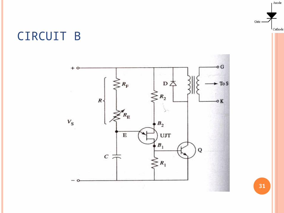
CIRCUIT B
31
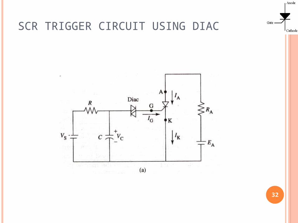
SCR TRIGGER CIRCUIT USING DIAC
32

SCR TRIGGER CIRCUIT USING OPTOCOUPLER
33
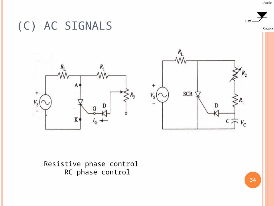
(C) AC SIGNALS
34
Resistive phase control RC phase control
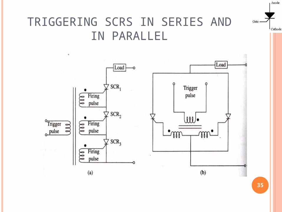
TRIGGERING SCRS IN SERIES AND IN PARALLEL
35
36
SCR Turnoff SCR Turnoff (Commutation) Circuits(Commutation) Circuits
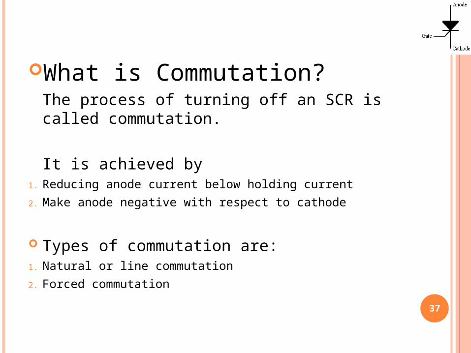
What is Commutation?The process of turning off an SCR is called commutation.
It is achieved by1. Reducing anode current below holding current
2. Make anode negative with respect to cathode
Types of commutation are:1. Natural or line commutation
2. Forced commutation
37

SCR TURNOFF METHODS
1. Diverting the anode current to an alternate path
2. Shorting the SCR from anode to cathode
3. Applying a reverse voltage (by making the cathode positive with respect to the anode) across the SCR
4. Forcing the anode current to zero for a brief period
5. Opening the external path from its anode supply voltage
6. Momentarily reducing supply voltage to zero38
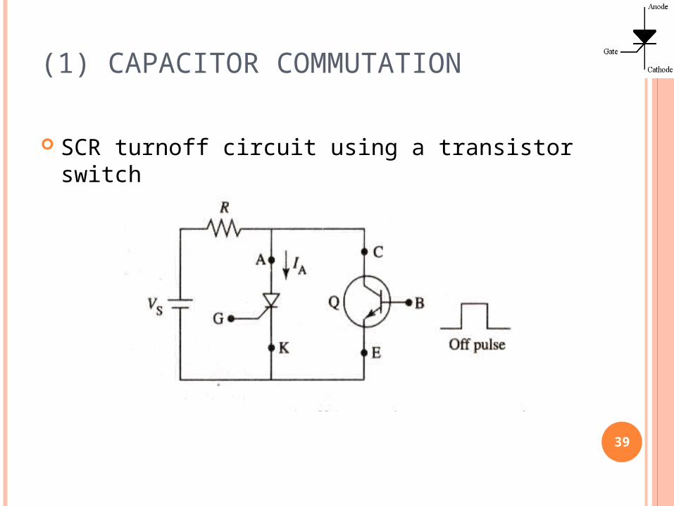
(1) CAPACITOR COMMUTATION
SCR turnoff circuit using a transistor switch
39
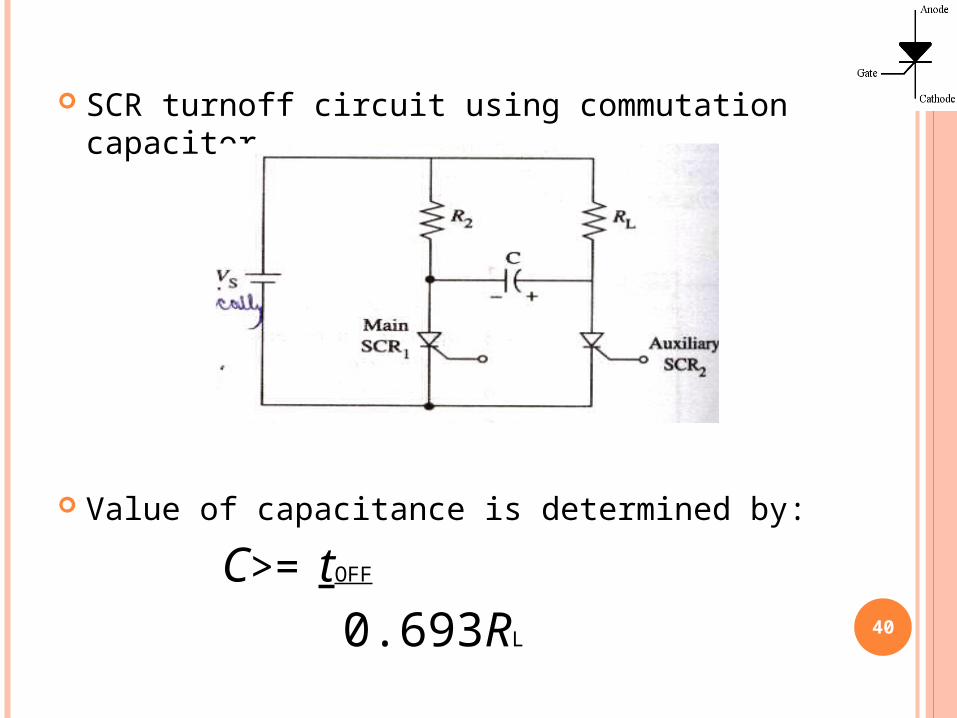
SCR turnoff circuit using commutation capacitor
Value of capacitance is determined by:
C>= tOFF
0.693RL40

(2) COMMUTATION BY EXTERNAL SOURCE
41

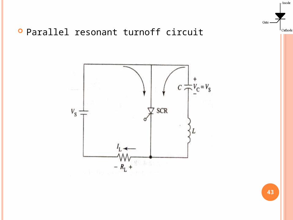
(3) COMMUTATION BY RESONANCE
Series resonant turnoff circuit
42
43
Parallel resonant turnoff circuit

(4) AC LINE COMMUTATION
44
45
Other members of Other members of Thyristor FamilyThyristor Family
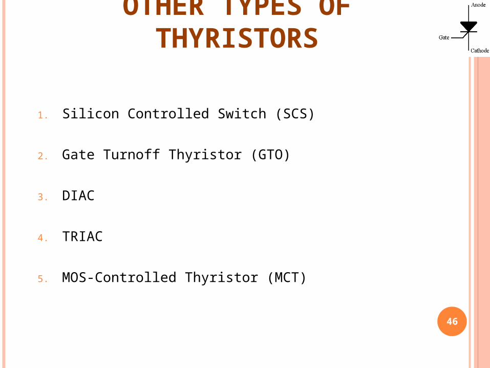
OTHER TYPES OF THYRISTORS
46
1. Silicon Controlled Switch (SCS)
2. Gate Turnoff Thyristor (GTO)
3. DIAC
4. TRIAC
5. MOS-Controlled Thyristor (MCT)
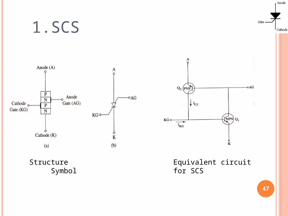
1.SCS
47
Structure Symbol
Equivalent circuit for SCS
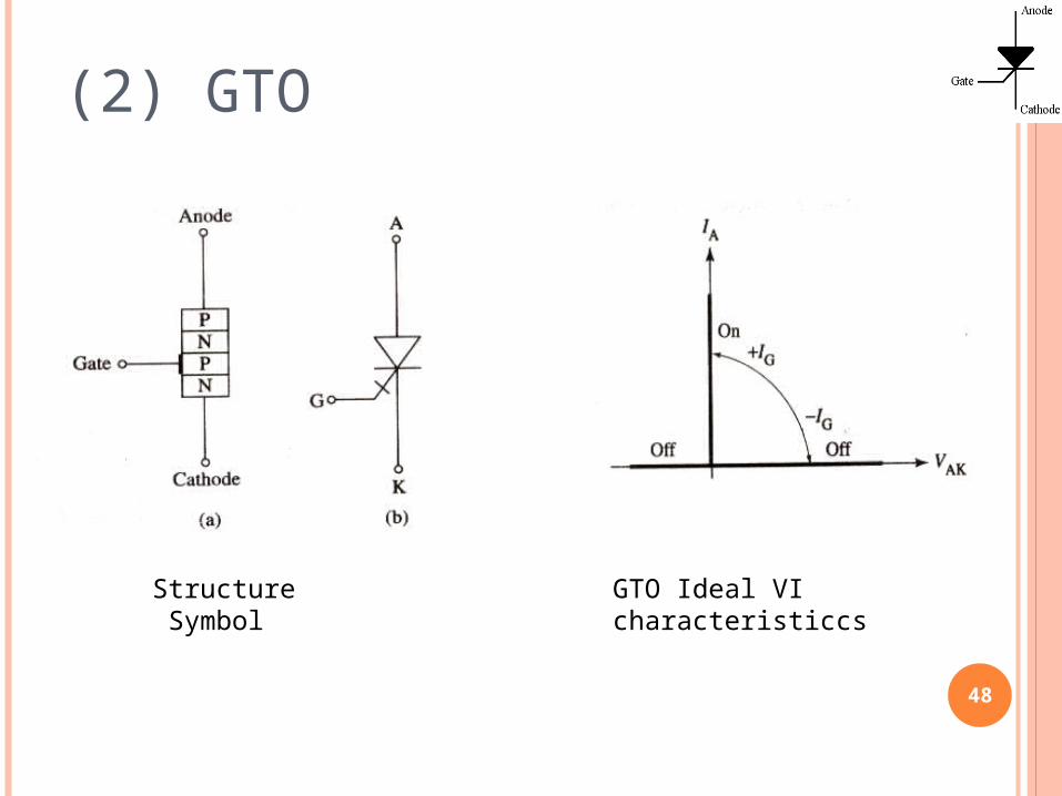
(2) GTO
48
Structure Symbol
GTO Ideal VI characteristiccs
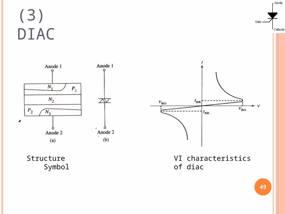
(3) DIAC
49
Structure Symbol
VI characteristics of diac

(4) TRIAC
50
Structure Symbol SCR equivalent circuit

TRIAC VI CHARACTERISTICS
51
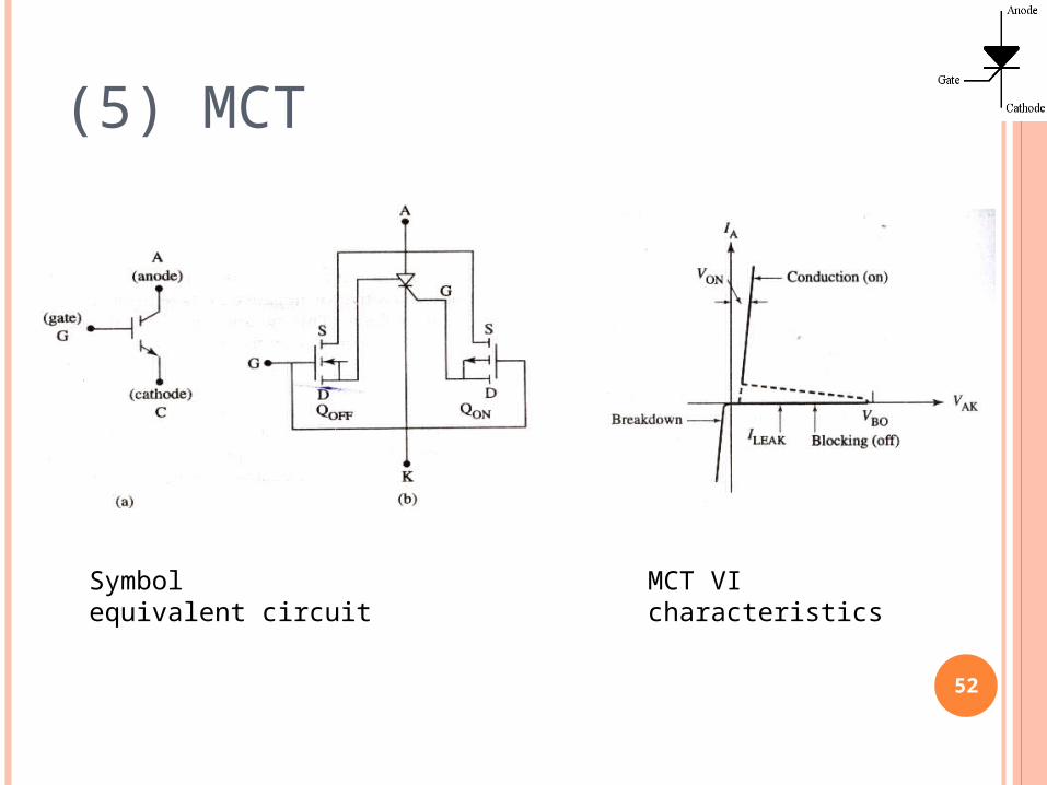
(5) MCT
52
Symbol equivalent circuit MCT VI characteristics

ASSIGNMENT#1
1. Does gate current has any effect on forward-breakover voltage? Justify the statement “Higher the gate current, lower is the forward breakover voltage.”
2. Discribe briefly following members of thyristor family.
Programmable Unijunction Transistor (PUT) Silicon Unilateral Switch (SUS) Static Induction Thyristor (SITH) Light Activated Thyristor (LASCR)
53